US5192894A - Device for the suppression of arcs - Google Patents
Device for the suppression of arcsDownload PDFInfo
- Publication number
- US5192894A US5192894AUS07/807,278US80727891AUS5192894AUS 5192894 AUS5192894 AUS 5192894AUS 80727891 AUS80727891 AUS 80727891AUS 5192894 AUS5192894 AUS 5192894A
- Authority
- US
- United States
- Prior art keywords
- voltage
- plasma
- circuit configuration
- differential amplifier
- stated
- Prior art date
- Legal status (The legal status is an assumption and is not a legal conclusion. Google has not performed a legal analysis and makes no representation as to the accuracy of the status listed.)
- Expired - Fee Related
Links
- 230000001629suppressionEffects0.000titleclaimsabstractdescription4
- 230000010354integrationEffects0.000claimsdescription3
- 239000000758substrateSubstances0.000description16
- VYPSYNLAJGMNEJ-UHFFFAOYSA-NSilicium dioxideChemical compoundO=[Si]=OVYPSYNLAJGMNEJ-UHFFFAOYSA-N0.000description8
- 238000010891electric arcMethods0.000description8
- 238000000034methodMethods0.000description7
- 238000004544sputter depositionMethods0.000description7
- 239000003990capacitorSubstances0.000description5
- 230000015572biosynthetic processEffects0.000description4
- 238000000576coating methodMethods0.000description4
- 229910052681coesiteInorganic materials0.000description4
- 229910052906cristobaliteInorganic materials0.000description4
- 239000007789gasSubstances0.000description4
- 230000008569processEffects0.000description4
- 239000000377silicon dioxideSubstances0.000description4
- 229910052682stishoviteInorganic materials0.000description4
- 229910052905tridymiteInorganic materials0.000description4
- 230000015556catabolic processEffects0.000description3
- 230000003247decreasing effectEffects0.000description3
- 238000010791quenchingMethods0.000description3
- XKRFYHLGVUSROY-UHFFFAOYSA-NArgonChemical compound[Ar]XKRFYHLGVUSROY-UHFFFAOYSA-N0.000description2
- XUIMIQQOPSSXEZ-UHFFFAOYSA-NSiliconChemical compound[Si]XUIMIQQOPSSXEZ-UHFFFAOYSA-N0.000description2
- QVGXLLKOCUKJST-UHFFFAOYSA-Natomic oxygenChemical compound[O]QVGXLLKOCUKJST-UHFFFAOYSA-N0.000description2
- 239000011248coating agentSubstances0.000description2
- 230000006378damageEffects0.000description2
- 230000000694effectsEffects0.000description2
- 239000011521glassSubstances0.000description2
- 238000010438heat treatmentMethods0.000description2
- 238000009434installationMethods0.000description2
- 239000000463materialSubstances0.000description2
- 239000001301oxygenSubstances0.000description2
- 229910052760oxygenInorganic materials0.000description2
- 239000002245particleSubstances0.000description2
- 230000000171quenching effectEffects0.000description2
- 229910052710siliconInorganic materials0.000description2
- 239000010703siliconSubstances0.000description2
- 230000009471actionEffects0.000description1
- 230000003321amplificationEffects0.000description1
- 229910052786argonInorganic materials0.000description1
- 230000008901benefitEffects0.000description1
- 239000012876carrier materialSubstances0.000description1
- 230000008859changeEffects0.000description1
- 239000002800charge carrierSubstances0.000description1
- 230000008878couplingEffects0.000description1
- 238000010168coupling processMethods0.000description1
- 238000005859coupling reactionMethods0.000description1
- 230000007423decreaseEffects0.000description1
- 230000001419dependent effectEffects0.000description1
- 238000011156evaluationMethods0.000description1
- 238000002474experimental methodMethods0.000description1
- 238000010304firingMethods0.000description1
- 238000011835investigationMethods0.000description1
- 238000002955isolationMethods0.000description1
- 230000033001locomotionEffects0.000description1
- 238000004519manufacturing processMethods0.000description1
- 239000002184metalSubstances0.000description1
- 238000004377microelectronicMethods0.000description1
- 238000003199nucleic acid amplification methodMethods0.000description1
- 230000001105regulatory effectEffects0.000description1
- 238000009751slip formingMethods0.000description1
- 230000001960triggered effectEffects0.000description1
Images
Classifications
- H—ELECTRICITY
- H01—ELECTRIC ELEMENTS
- H01J—ELECTRIC DISCHARGE TUBES OR DISCHARGE LAMPS
- H01J37/00—Discharge tubes with provision for introducing objects or material to be exposed to the discharge, e.g. for the purpose of examination or processing thereof
- H01J37/32—Gas-filled discharge tubes
- H01J37/34—Gas-filled discharge tubes operating with cathodic sputtering
- H01J37/3411—Constructional aspects of the reactor
- H01J37/3444—Associated circuits
- H—ELECTRICITY
- H02—GENERATION; CONVERSION OR DISTRIBUTION OF ELECTRIC POWER
- H02H—EMERGENCY PROTECTIVE CIRCUIT ARRANGEMENTS
- H02H7/00—Emergency protective circuit arrangements specially adapted for specific types of electric machines or apparatus or for sectionalised protection of cable or line systems, and effecting automatic switching in the event of an undesired change from normal working conditions
- H—ELECTRICITY
- H01—ELECTRIC ELEMENTS
- H01J—ELECTRIC DISCHARGE TUBES OR DISCHARGE LAMPS
- H01J2237/00—Discharge tubes exposing object to beam, e.g. for analysis treatment, etching, imaging
- H01J2237/02—Details
- H01J2237/0203—Protection arrangements
- H01J2237/0206—Extinguishing, preventing or controlling unwanted discharges
Definitions
- the inventionrelates to an arc suppression circuit according to the preamble of patent claim 1.
- the inventionis based on the task of creating an improved circuit configuration for quenching arcs in plasma arrangements.
- the advantage achieved with the inventionresides in particular therein that even when sputtering difficult materials, for example SiO 2 , high coating rates are possible because the sputtering process is only interrupted for a very short time.
- SiO 2Si atoms are knocked out from a target of highest grade silicon disposed in an argon/oxygen atmosphere of 10 -3 to 10 -1 mbars, which combine with oxygen to form SiO 2 which is deposited on a substrate.
- the arc formationcan, as experiments have shown, occur specifically so that after a first voltage return the cathode voltage remains for several milliseconds at a voltage value of approximately 250 V. This voltage value is still within the acceptable operating range of the cathode. After that the cathode voltage breaks down to an arc value of 30 to 50 V. This intermediate stage is physically interpreted with the build-up of a charge carrier cloud at the cathode.
- This intermediate stageis physically interpreted with the build-up of a charge carrier cloud at the cathode.
- the formation of a complete arcleads to local heating of the cathode surface and, consequently, of the target which is also referred to as "hot spot". In order to continue making possible the sputtering operation this hot spot must have cooled before the cathode voltage is switched on again so that it cannot effect thermal emission of electrons. The sooner an arc is recognized and the cathode current switched off, the less is the probability that significant heating occurs.
- an arccan be recognized and signaled to a switching device before the current strength in the arc has increased so much that damages in the target and/or substrate area can occur such as for example material splashes from target to substrate or splits off the target. Since no fixed limits for current and voltage are monitored in the invention, but rather the change of the voltage over time is checked, considerably earlier recognition of the arc is possible.
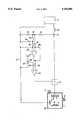
- the single FIGUREshows the principle of a sputtering installation with the circuitry according to the invention.
- a substrate holder 4on which is disposed a substrate 5.
- the substrate 5comprises for example glass or is a synthetic film or a silicon wafer of microelectronic fabrication.
- the vacuum chamber 1comprises preferably metal and is at ground. Opposing the substrate 5 is a cathode 6 with a target 7. The associated anode 8 is disposed laterally to substrate 5.
- a resistor 13which is connected with a second resistor 14 which, in turn, is connected with the cathode and the positive output of the voltage source 11.
- a further resistor 16is connected which is connected to a first input terminal of a differential amplifier 17.
- the second input of this differential amplifieris connected via a resistor 18 and a resistor 19 likewise to the connecting line 15.
- a capacitor 20is connected with its one terminal to the connecting line between resistor 19 and resistor 18 and with its other terminal to the connecting line 21 between the positive output of the voltage source 11 and the anode 8.
- a resistor 22which is connected with the second input of the differential amplifier 17.
- the output of the differential amplifier 17leads via a resistor 23 to an input of a further differential amplifier 24 whose further input is connected via a resistor 25 with the tap 26 of a potentiometer 27.
- This potentiometer 27is, on the one hand, connected to the negative terminal of a dc voltage source of, for example 15 V, and, on the other hand, to the line 21.
- the output of the differential amplifier 17is fed back via a resistor 28 to the negative input of this amplifier 17.
- the choke 10serves the function of increasing the dynamic impedance of the dc voltage source 11 so that the cathode current can increase only insignificantly within a given time interval.
- switch 9it is possible to interrupt the cathode current if an actual or developing arc discharge is detected.
- the switch 9can also be a component part of the voltage source 11 or can be disposed between the voltage source 11 and the choke 10. Moreover, instead of an isolation of the voltage source 11 from the cathode it could also effect a shortcircuit between anode 8 and cathode 6.
- the two resistors 13, 14represent a voltage divider while the resistor 19 represents, together with the capacitor 20, an RC element which integrates the cathode voltage decreased to a processable level.
- the integration time constant resulting from the mathematical product of the resistance of resistor 19 and the capacitance of capacitor 20is selected so that at a given lower limit value for the slope of the voltage drop and at a fixed minimal length of time of the voltage drop the signal level set for triggering the switch 9 is obtained.
- the voltage integrated at capacitor 20is compared by means of conventional differential amplification circuits 16, 17, 18, 22, 28 with the actual voltage value.
- the output voltage of the differential amplifier 17is evaluated with a conventional trigger circuit 23, 24, 25. If the trigger switching point is exceeded, switch 9 is triggered.
- the lower limit value for the slope of the drop of the cathode voltageis defined as 2 V/us, the minimum interval as 5 us.
- Criterion for the switching actionconsequently is exceeding a threshold value of the difference voltage formed from the instantaneous voltage minus the mean value of the voltage which is continuously formed over a defined period of time.
Landscapes
- Physics & Mathematics (AREA)
- Engineering & Computer Science (AREA)
- Plasma & Fusion (AREA)
- Chemical & Material Sciences (AREA)
- Analytical Chemistry (AREA)
- Plasma Technology (AREA)
- Physical Vapour Deposition (AREA)
- Control Of Indicators Other Than Cathode Ray Tubes (AREA)
Abstract
Description
Claims (6)
Applications Claiming Priority (2)
| Application Number | Priority Date | Filing Date | Title |
|---|---|---|---|
| DE4127504 | 1991-08-20 | ||
| DE4127504ADE4127504A1 (en) | 1991-08-20 | 1991-08-20 | DEVICE FOR SUPPRESSING ARCES |
Publications (1)
| Publication Number | Publication Date |
|---|---|
| US5192894Atrue US5192894A (en) | 1993-03-09 |
Family
ID=6438674
Family Applications (1)
| Application Number | Title | Priority Date | Filing Date |
|---|---|---|---|
| US07/807,278Expired - Fee RelatedUS5192894A (en) | 1991-08-20 | 1991-12-13 | Device for the suppression of arcs |
Country Status (5)
| Country | Link |
|---|---|
| US (1) | US5192894A (en) |
| EP (1) | EP0528163B1 (en) |
| JP (1) | JPH06132095A (en) |
| DE (2) | DE4127504A1 (en) |
| ES (1) | ES2079749T3 (en) |
Cited By (65)
| Publication number | Priority date | Publication date | Assignee | Title |
|---|---|---|---|---|
| US5286360A (en)* | 1992-01-29 | 1994-02-15 | Leybold Aktiengesellschaft | Apparatus for coating a substrate, especially with electrically nonconductive coatings |
| US5352954A (en)* | 1992-03-11 | 1994-10-04 | Proel Technologie S.P.A. | Plasma generator and associated ionization method |
| US5427669A (en)* | 1992-12-30 | 1995-06-27 | Advanced Energy Industries, Inc. | Thin film DC plasma processing system |
| DE4420951A1 (en)* | 1994-06-16 | 1995-12-21 | Leybold Ag | Appts. for detecting micro-arcs in sputtering units |
| DE4441206A1 (en)* | 1994-11-19 | 1996-05-23 | Leybold Ag | Device for the suppression of rollovers in cathode sputtering devices |
| US5576939A (en)* | 1995-05-05 | 1996-11-19 | Drummond; Geoffrey N. | Enhanced thin film DC plasma power supply |
| US5584974A (en)* | 1995-10-20 | 1996-12-17 | Eni | Arc control and switching element protection for pulsed dc cathode sputtering power supply |
| US5645698A (en)* | 1992-09-30 | 1997-07-08 | Advanced Energy Industries, Inc. | Topographically precise thin film coating system |
| US5682067A (en)* | 1996-06-21 | 1997-10-28 | Sierra Applied Sciences, Inc. | Circuit for reversing polarity on electrodes |
| US5698082A (en)* | 1993-08-04 | 1997-12-16 | Balzers Und Leybold | Method and apparatus for coating substrates in a vacuum chamber, with a system for the detection and suppression of undesirable arcing |
| US5718813A (en)* | 1992-12-30 | 1998-02-17 | Advanced Energy Industries, Inc. | Enhanced reactive DC sputtering system |
| US5882492A (en)* | 1996-06-21 | 1999-03-16 | Sierra Applied Sciences, Inc. | A.C. plasma processing system |
| WO1999014394A1 (en)* | 1997-09-17 | 1999-03-25 | Tokyo Electron Limited | Device and method for detecting and preventing arcing in rf plasma systems |
| US5889391A (en)* | 1997-11-07 | 1999-03-30 | Sierra Applied Sciences, Inc. | Power supply having combined regulator and pulsing circuits |
| US5910886A (en)* | 1997-11-07 | 1999-06-08 | Sierra Applied Sciences, Inc. | Phase-shift power supply |
| US5917286A (en)* | 1996-05-08 | 1999-06-29 | Advanced Energy Industries, Inc. | Pulsed direct current power supply configurations for generating plasmas |
| US5948224A (en)* | 1992-03-24 | 1999-09-07 | Balzers Aktiengsellschaft | Method of controlling a treatment process and vacuum treatment apparatus |
| US5990668A (en)* | 1997-11-07 | 1999-11-23 | Sierra Applied Sciences, Inc. | A.C. power supply having combined regulator and pulsing circuits |
| US5993613A (en)* | 1997-11-07 | 1999-11-30 | Sierra Applied Sciences, Inc. | Method and apparatus for periodic polarity reversal during an active state |
| US6007879A (en)* | 1995-04-07 | 1999-12-28 | Advanced Energy Industries, Inc. | Adjustable energy quantum thin film plasma processing system |
| US6011704A (en)* | 1997-11-07 | 2000-01-04 | Sierra Applied Sciences, Inc. | Auto-ranging power supply |
| US6090246A (en)* | 1998-01-20 | 2000-07-18 | Micron Technology, Inc. | Methods and apparatus for detecting reflected neutrals in a sputtering process |
| US6217717B1 (en)* | 1992-12-30 | 2001-04-17 | Advanced Energy Industries, Inc. | Periodically clearing thin film plasma processing system |
| WO2001027970A1 (en)* | 1999-10-13 | 2001-04-19 | Unaxis Deutschland Gmbh | Electric supply unit and a method for reducing sparking during sputtering |
| US6280579B1 (en)* | 1997-12-19 | 2001-08-28 | Applied Materials, Inc. | Target misalignment detector |
| US6506288B1 (en)* | 1993-01-04 | 2003-01-14 | Unaxis Balzers Aktiengesellschaft | Optical film material especially TiO2 or Ta2O5 optical waveguide layer and method for producing such |
| US20040112735A1 (en)* | 2002-12-17 | 2004-06-17 | Applied Materials, Inc. | Pulsed magnetron for sputter deposition |
| WO2004003968A3 (en)* | 2002-06-28 | 2004-09-10 | Tokyo Electron Ltd | Method and system for arc suppression in a plasma processing system |
| US6943317B1 (en)* | 2004-07-02 | 2005-09-13 | Advanced Energy Industries, Inc. | Apparatus and method for fast arc extinction with early shunting of arc current in plasma |
| US20050236266A1 (en)* | 2002-06-19 | 2005-10-27 | Poole John E | Sputter target monitoring system |
| US20060011591A1 (en)* | 2003-08-18 | 2006-01-19 | Mks Instruments, Inc. | Control of plasma transitions in sputter processing systems |
| US20060241879A1 (en)* | 2005-04-22 | 2006-10-26 | Advanced Energy Industries, Inc. | Arc detection and handling in radio frequency power applications |
| WO2006058169A3 (en)* | 2004-11-23 | 2006-11-30 | Ibis Technology Corp | Power sag detection and control in ion implanting systems |
| US20060283702A1 (en)* | 2005-06-21 | 2006-12-21 | Applied Materials, Inc. | Random pulsed DC power supply |
| US20070073498A1 (en)* | 2004-03-25 | 2007-03-29 | Huettinger Elektronik Gmbh + Co. Kg | Method of detecting arc discharges in a plasma process |
| US20070168143A1 (en)* | 2005-12-22 | 2007-07-19 | Huettinger Elektronik Gmbh + Co. Kg | Method and Device for Detecting Arcs |
| WO2007106395A3 (en)* | 2006-03-14 | 2007-12-13 | Axcelis Tech Inc | Arc quenching circuit to mitigate ion beam disruption |
| US20080000768A1 (en)* | 2006-06-30 | 2008-01-03 | Stimson Bradley O | Electrically Coupled Target Panels |
| US20080035470A1 (en)* | 2005-04-12 | 2008-02-14 | Hauzer Techno-Coating B.V. | Device For Plasma-Treating And/Or Coating Work Pieces |
| US20080061794A1 (en)* | 2006-09-13 | 2008-03-13 | Joshua Brian Pankratz | System and Method for Managing Power Supplied to a Plasma Chamber |
| US20080067433A1 (en)* | 2006-03-14 | 2008-03-20 | Axcelis Technologies, Inc. | System and method of ion beam control in response to a beam glitch |
| US20080122369A1 (en)* | 2006-11-24 | 2008-05-29 | HUETTINGER ELEKTRONIK GMBH + CO. KG | Controlled plasma power supply |
| US20080121625A1 (en)* | 2006-11-28 | 2008-05-29 | HUETTINGER ELEKTRONIK GMBH + CO. KG | Detecting arc discharges |
| US20080121517A1 (en)* | 2006-11-23 | 2008-05-29 | Moritz Nitschke | Method for operating a plasma process and arc discharge detection device |
| US20080133154A1 (en)* | 2002-04-12 | 2008-06-05 | Schneider Electric | System and Method for Detecting Non-Cathode Arcing in a Plasma Generation Apparatus |
| US20080203070A1 (en)* | 2007-02-22 | 2008-08-28 | Milan Ilic | Arc recovery without over-voltage for plasma chamber power supplies using a shunt switch |
| US20080216745A1 (en)* | 2005-05-06 | 2008-09-11 | Peter Wiedemuth | Arc Suppression |
| US20080257869A1 (en)* | 2006-12-14 | 2008-10-23 | Huettinger Elektronik Gmbh + Co. Kg | Responding to arc discharges |
| US20080309402A1 (en)* | 2007-05-12 | 2008-12-18 | Huettinger Electronic Sp. Z O.O. | Extinction of plasma arcs |
| US20090160417A1 (en)* | 2007-12-24 | 2009-06-25 | Huettinger Electronic Sp. Z.O.O. (Tple) | Current limiting device for plasma power supply |
| US20090280581A1 (en)* | 2008-05-12 | 2009-11-12 | Lam Research Corporation | Detection of arcing events in wafer plasma processing through monitoring of trace gas concentrations |
| US20100026186A1 (en)* | 2008-07-31 | 2010-02-04 | Advanced Energy Industries, Inc. | Power supply ignition system and method |
| US20100134933A1 (en)* | 2004-11-10 | 2010-06-03 | Frederick Jerome Potter | Arc detection circuit |
| US20100211230A1 (en)* | 2009-02-17 | 2010-08-19 | Albert Bulliard | power supply device for plasma processing |
| US20110019332A1 (en)* | 2004-02-22 | 2011-01-27 | Zond, Inc. | Methods And Apparatus For Generating Strongly-Ionized Plasmas With Ionizational Instabilities |
| US7929261B2 (en) | 2007-03-08 | 2011-04-19 | Huettinger Elektronik Gmbh + Co. Kg | Suppressing arc discharges |
| US7981257B2 (en) | 2002-04-12 | 2011-07-19 | Schneider Electric USA, Inc. | Current-based method and apparatus for detecting and classifying arcs |
| US20110222191A1 (en)* | 2010-03-12 | 2011-09-15 | Reinhold Henke | Two Terminal Arc Suppressor |
| US8395078B2 (en) | 2008-12-05 | 2013-03-12 | Advanced Energy Industries, Inc | Arc recovery with over-voltage protection for plasma-chamber power supplies |
| US8552665B2 (en) | 2010-08-20 | 2013-10-08 | Advanced Energy Industries, Inc. | Proactive arc management of a plasma load |
| CN103346548A (en)* | 2013-07-05 | 2013-10-09 | 苏州贝昂科技有限公司 | Discharging monitoring and protecting circuit on high-voltage ion purifier |
| US8796933B2 (en) | 2010-12-08 | 2014-08-05 | Applied Materials, Inc. | Generating plasmas in pulsed power systems |
| US9735568B2 (en) | 2013-06-04 | 2017-08-15 | Suzhou Beiang Technology Ltd. | Ionic wind purifier and discharge monitoring and protective circuit of high-voltage ion purifier |
| US10704136B2 (en) | 2013-03-05 | 2020-07-07 | Raytheon Technologies Corporation | Cathodic arc deposition stinger |
| US11013075B2 (en) | 2018-12-20 | 2021-05-18 | Nxp Usa, Inc. | RF apparatus with arc prevention using non-linear devices |
Families Citing this family (11)
| Publication number | Priority date | Publication date | Assignee | Title |
|---|---|---|---|---|
| DE4326100B4 (en)* | 1993-08-04 | 2006-03-23 | Unaxis Deutschland Holding Gmbh | Method and apparatus for coating substrates in a vacuum chamber, with means for detecting and suppressing unwanted arcing |
| DE4438463C1 (en)* | 1994-10-27 | 1996-02-15 | Fraunhofer Ges Forschung | Method and circuit for bipolar pulsed energy feed to low-pressure plasmas |
| AT405582B (en)* | 1995-10-30 | 1999-09-27 | Ruebig Ges M B H & Co Kg | DEVICE FOR TREATING A WORKPIECE IN A GAS DISCHARGE |
| DE19651615C1 (en)* | 1996-12-12 | 1997-07-10 | Fraunhofer Ges Forschung | Sputter coating to produce carbon layer for e.g. magnetic heads |
| DE19651811B4 (en)* | 1996-12-13 | 2006-08-31 | Unaxis Deutschland Holding Gmbh | Device for covering a substrate with thin layers |
| DE19702187C2 (en)* | 1997-01-23 | 2002-06-27 | Fraunhofer Ges Forschung | Method and device for operating magnetron discharges |
| DE19848636C2 (en)* | 1998-10-22 | 2001-07-26 | Fraunhofer Ges Forschung | Method for monitoring an AC voltage discharge on a double electrode |
| DE10034895C2 (en)* | 2000-07-18 | 2002-11-14 | Fraunhofer Ges Forschung | Method for detecting rollovers in pulsed plasmas |
| DE102008060838A1 (en) | 2008-12-05 | 2010-06-10 | Zounek, Alexis, Dr. | Coating substrates, comprises generating plasma with positively charged ion that is accelerated on substrate by negative bias potential, and reducing and/or compensating positive loading of substrate by irradiating substrate with electron |
| DE102017128402B4 (en) | 2017-11-30 | 2025-05-22 | Pva Tepla Ag | Arc-suppressing pulse plasma system and method for suppressing a developing arc |
| JP7468241B2 (en)* | 2020-08-12 | 2024-04-16 | 株式会社島津製作所 | Film forming apparatus, film forming method, and program |
Citations (9)
| Publication number | Priority date | Publication date | Assignee | Title |
|---|---|---|---|---|
| US3909664A (en)* | 1973-09-17 | 1975-09-30 | Outboard Marine Corp | Plasma spraying method and apparatus |
| US4648952A (en)* | 1984-11-26 | 1987-03-10 | Vmei "Lenin" | Method of controlling thermochemical treatment of workpieces in glow discharge in a treating gas medium and device which embodies this method |
| US4733137A (en)* | 1986-03-14 | 1988-03-22 | Walker Magnetics Group, Inc. | Ion nitriding power supply |
| US4786844A (en)* | 1987-03-30 | 1988-11-22 | Rpc Industries | Wire ion plasma gun |
| US4935661A (en)* | 1985-06-29 | 1990-06-19 | Stc Plc | Pulsed plasma apparatus and process |
| US4936960A (en)* | 1989-01-03 | 1990-06-26 | Advanced Energy Industries, Inc. | Method and apparatus for recovery from low impedance condition during cathodic arc processes |
| US5025135A (en)* | 1988-06-23 | 1991-06-18 | Leybold Aktiengesellschaft | Circuit configuration for the recognition of a plasma |
| US5037522A (en)* | 1990-07-24 | 1991-08-06 | Vergason Technology, Inc. | Electric arc vapor deposition device |
| US5053725A (en)* | 1989-07-18 | 1991-10-01 | Leybold Ag | Circuit configuration for the automatic tuning of a matching network |
Family Cites Families (5)
| Publication number | Priority date | Publication date | Assignee | Title |
|---|---|---|---|---|
| DE3220434A1 (en)* | 1982-05-29 | 1983-12-01 | Robert Bosch Gmbh, 7000 Stuttgart | METHOD FOR MONITORING A MEASUREMENT |
| BG41745A1 (en)* | 1984-12-29 | 1987-08-14 | Minchev | Device for discontinuing of arc dicharges in gas dicharge vessel |
| DE3538494A1 (en)* | 1985-10-30 | 1987-05-07 | Boehringer Andreas | Electrical circuit arrangement, which is supplied from a DC voltage source, for supplying a load two-pole network with a direct current which is impressed but can be interrupted or a block-form alternating current which is impressed but can be interrupted, with adjustable limiting of the voltages on the load two-pole network and on the electronic one-way switches which are used |
| FR2648001B1 (en)* | 1989-05-31 | 1991-09-27 | Breda Jean Pierre | DIRECT CURRENT SUPPLY OF PLASMA ELECTRODES AND METHOD FOR REGENERATING PLASMA |
| US5241152A (en)* | 1990-03-23 | 1993-08-31 | Anderson Glen L | Circuit for detecting and diverting an electrical arc in a glow discharge apparatus |
- 1991
- 1991-08-20DEDE4127504Apatent/DE4127504A1/ennot_activeWithdrawn
- 1991-12-13USUS07/807,278patent/US5192894A/ennot_activeExpired - Fee Related
- 1992
- 1992-07-10EPEP92111749Apatent/EP0528163B1/ennot_activeExpired - Lifetime
- 1992-07-10ESES92111749Tpatent/ES2079749T3/ennot_activeExpired - Lifetime
- 1992-07-10DEDE59203659Tpatent/DE59203659D1/ennot_activeExpired - Fee Related
- 1992-08-11JPJP4235443Apatent/JPH06132095A/enactivePending
Patent Citations (10)
| Publication number | Priority date | Publication date | Assignee | Title |
|---|---|---|---|---|
| US3909664A (en)* | 1973-09-17 | 1975-09-30 | Outboard Marine Corp | Plasma spraying method and apparatus |
| US4648952A (en)* | 1984-11-26 | 1987-03-10 | Vmei "Lenin" | Method of controlling thermochemical treatment of workpieces in glow discharge in a treating gas medium and device which embodies this method |
| US4935661A (en)* | 1985-06-29 | 1990-06-19 | Stc Plc | Pulsed plasma apparatus and process |
| US4733137A (en)* | 1986-03-14 | 1988-03-22 | Walker Magnetics Group, Inc. | Ion nitriding power supply |
| US4786844A (en)* | 1987-03-30 | 1988-11-22 | Rpc Industries | Wire ion plasma gun |
| US5025135A (en)* | 1988-06-23 | 1991-06-18 | Leybold Aktiengesellschaft | Circuit configuration for the recognition of a plasma |
| US4936960A (en)* | 1989-01-03 | 1990-06-26 | Advanced Energy Industries, Inc. | Method and apparatus for recovery from low impedance condition during cathodic arc processes |
| US5053725A (en)* | 1989-07-18 | 1991-10-01 | Leybold Ag | Circuit configuration for the automatic tuning of a matching network |
| US5037522A (en)* | 1990-07-24 | 1991-08-06 | Vergason Technology, Inc. | Electric arc vapor deposition device |
| US5037522B1 (en)* | 1990-07-24 | 1996-07-02 | Vergason Technology Inc | Electric arc vapor deposition device |
Non-Patent Citations (2)
| Title |
|---|
| "The MDX as a Strategic Tool in Reducing Arcing", by Douglas S. Schatz in 1985. |
| The MDX as a Strategic Tool in Reducing Arcing , by Douglas S. Schatz in 1985.* |
Cited By (128)
| Publication number | Priority date | Publication date | Assignee | Title |
|---|---|---|---|---|
| US5286360A (en)* | 1992-01-29 | 1994-02-15 | Leybold Aktiengesellschaft | Apparatus for coating a substrate, especially with electrically nonconductive coatings |
| US5352954A (en)* | 1992-03-11 | 1994-10-04 | Proel Technologie S.P.A. | Plasma generator and associated ionization method |
| US20030178300A1 (en)* | 1992-03-24 | 2003-09-25 | Hans Signer | Method of manufacturing an object in a vacuum recipient |
| US5948224A (en)* | 1992-03-24 | 1999-09-07 | Balzers Aktiengsellschaft | Method of controlling a treatment process and vacuum treatment apparatus |
| US6878248B2 (en) | 1992-03-24 | 2005-04-12 | Hans Signer | Method of manufacturing an object in a vacuum recipient |
| US6176979B1 (en)* | 1992-03-24 | 2001-01-23 | Balzers Aktiengesellschaft | Method of manufacturing an object in a vacuum recipient |
| US6149783A (en)* | 1992-03-24 | 2000-11-21 | Balzers Aktiengesellschaft | Vacuum treatment apparatus |
| US6120656A (en)* | 1992-09-30 | 2000-09-19 | Advanced Energy Industries, Inc. | Topographically precise thin film coating system |
| US5645698A (en)* | 1992-09-30 | 1997-07-08 | Advanced Energy Industries, Inc. | Topographically precise thin film coating system |
| US6521099B1 (en) | 1992-12-30 | 2003-02-18 | Advanced Energy Industries, Inc. | Periodically clearing thin film plasma processing system |
| US5718813A (en)* | 1992-12-30 | 1998-02-17 | Advanced Energy Industries, Inc. | Enhanced reactive DC sputtering system |
| US5427669A (en)* | 1992-12-30 | 1995-06-27 | Advanced Energy Industries, Inc. | Thin film DC plasma processing system |
| US6024844A (en)* | 1992-12-30 | 2000-02-15 | Advanced Energy Industries, Inc. | Enhanced reactive DC sputtering system |
| US6217717B1 (en)* | 1992-12-30 | 2001-04-17 | Advanced Energy Industries, Inc. | Periodically clearing thin film plasma processing system |
| US6506288B1 (en)* | 1993-01-04 | 2003-01-14 | Unaxis Balzers Aktiengesellschaft | Optical film material especially TiO2 or Ta2O5 optical waveguide layer and method for producing such |
| EP0692138B1 (en)* | 1993-04-02 | 2004-01-21 | Advanced Energy Industries, Inc. | Reactive dc sputtering system |
| US6001224A (en)* | 1993-04-02 | 1999-12-14 | Advanced Energy Industries, Inc. | Enhanced reactive DC sputtering system |
| US5698082A (en)* | 1993-08-04 | 1997-12-16 | Balzers Und Leybold | Method and apparatus for coating substrates in a vacuum chamber, with a system for the detection and suppression of undesirable arcing |
| DE4420951C2 (en)* | 1994-06-16 | 1998-01-22 | Leybold Ag | Device for detecting micro-flashovers in atomizing systems |
| DE4420951A1 (en)* | 1994-06-16 | 1995-12-21 | Leybold Ag | Appts. for detecting micro-arcs in sputtering units |
| US5611899A (en)* | 1994-11-19 | 1997-03-18 | Leybold Aktiengesellschaft | Device for suppressing flashovers in cathode sputtering installations |
| DE4441206A1 (en)* | 1994-11-19 | 1996-05-23 | Leybold Ag | Device for the suppression of rollovers in cathode sputtering devices |
| US6368477B1 (en) | 1995-04-07 | 2002-04-09 | Advanced Energy Industries, Inc. | Adjustable energy quantum thin film plasma processing system |
| US6007879A (en)* | 1995-04-07 | 1999-12-28 | Advanced Energy Industries, Inc. | Adjustable energy quantum thin film plasma processing system |
| US5576939A (en)* | 1995-05-05 | 1996-11-19 | Drummond; Geoffrey N. | Enhanced thin film DC plasma power supply |
| GB2306511B (en)* | 1995-10-20 | 1999-06-09 | Eni Inc | Arc control and switching element protection for pulsed DC power supply |
| US5584974A (en)* | 1995-10-20 | 1996-12-17 | Eni | Arc control and switching element protection for pulsed dc cathode sputtering power supply |
| US6222321B1 (en) | 1996-05-08 | 2001-04-24 | Advanced Energy Industries, Inc. | Plasma generator pulsed direct current supply in a bridge configuration |
| US5917286A (en)* | 1996-05-08 | 1999-06-29 | Advanced Energy Industries, Inc. | Pulsed direct current power supply configurations for generating plasmas |
| US5815388A (en)* | 1996-06-21 | 1998-09-29 | Sierra Applied Sciences, Inc. | Polarity reversing circuit having energy compensation |
| US5682067A (en)* | 1996-06-21 | 1997-10-28 | Sierra Applied Sciences, Inc. | Circuit for reversing polarity on electrodes |
| US5882492A (en)* | 1996-06-21 | 1999-03-16 | Sierra Applied Sciences, Inc. | A.C. plasma processing system |
| US6332961B1 (en) | 1997-09-17 | 2001-12-25 | Tokyo Electron Limited | Device and method for detecting and preventing arcing in RF plasma systems |
| WO1999014394A1 (en)* | 1997-09-17 | 1999-03-25 | Tokyo Electron Limited | Device and method for detecting and preventing arcing in rf plasma systems |
| US6011704A (en)* | 1997-11-07 | 2000-01-04 | Sierra Applied Sciences, Inc. | Auto-ranging power supply |
| US5990668A (en)* | 1997-11-07 | 1999-11-23 | Sierra Applied Sciences, Inc. | A.C. power supply having combined regulator and pulsing circuits |
| US5910886A (en)* | 1997-11-07 | 1999-06-08 | Sierra Applied Sciences, Inc. | Phase-shift power supply |
| US5889391A (en)* | 1997-11-07 | 1999-03-30 | Sierra Applied Sciences, Inc. | Power supply having combined regulator and pulsing circuits |
| US5993613A (en)* | 1997-11-07 | 1999-11-30 | Sierra Applied Sciences, Inc. | Method and apparatus for periodic polarity reversal during an active state |
| US6280579B1 (en)* | 1997-12-19 | 2001-08-28 | Applied Materials, Inc. | Target misalignment detector |
| US6090246A (en)* | 1998-01-20 | 2000-07-18 | Micron Technology, Inc. | Methods and apparatus for detecting reflected neutrals in a sputtering process |
| US6740207B2 (en) | 1999-10-13 | 2004-05-25 | Unaxis Deutschland Gmbh | Electric supply unit and method for reducing arcing during sputtering |
| WO2001027970A1 (en)* | 1999-10-13 | 2001-04-19 | Unaxis Deutschland Gmbh | Electric supply unit and a method for reducing sparking during sputtering |
| US7988833B2 (en) | 2002-04-12 | 2011-08-02 | Schneider Electric USA, Inc. | System and method for detecting non-cathode arcing in a plasma generation apparatus |
| US20080133154A1 (en)* | 2002-04-12 | 2008-06-05 | Schneider Electric | System and Method for Detecting Non-Cathode Arcing in a Plasma Generation Apparatus |
| US7981257B2 (en) | 2002-04-12 | 2011-07-19 | Schneider Electric USA, Inc. | Current-based method and apparatus for detecting and classifying arcs |
| US20050236266A1 (en)* | 2002-06-19 | 2005-10-27 | Poole John E | Sputter target monitoring system |
| WO2004003968A3 (en)* | 2002-06-28 | 2004-09-10 | Tokyo Electron Ltd | Method and system for arc suppression in a plasma processing system |
| US7199327B2 (en) | 2002-06-28 | 2007-04-03 | Tokyo Electron Limited | Method and system for arc suppression in a plasma processing system |
| US20060081564A1 (en)* | 2002-06-28 | 2006-04-20 | Tokyo Electron Limited | Method and system for arc suppression in a plasma processing system |
| US20040112735A1 (en)* | 2002-12-17 | 2004-06-17 | Applied Materials, Inc. | Pulsed magnetron for sputter deposition |
| US8089026B2 (en)* | 2003-08-18 | 2012-01-03 | Mks Instruments, Inc. | Methods for control of plasma transitions in sputter processing systems using a resonant circuit |
| US20060011591A1 (en)* | 2003-08-18 | 2006-01-19 | Mks Instruments, Inc. | Control of plasma transitions in sputter processing systems |
| US8125155B2 (en)* | 2004-02-22 | 2012-02-28 | Zond, Inc. | Methods and apparatus for generating strongly-ionized plasmas with ionizational instabilities |
| US20110019332A1 (en)* | 2004-02-22 | 2011-01-27 | Zond, Inc. | Methods And Apparatus For Generating Strongly-Ionized Plasmas With Ionizational Instabilities |
| US8007641B2 (en) | 2004-03-25 | 2011-08-30 | Huettinger Elektronik Gmbh + Co. Kg | Method of detecting arc discharges in a plasma process |
| US9484189B2 (en) | 2004-03-25 | 2016-11-01 | Trumpf Huettinger Gmbh + Co. Kg | Method of detecting arc discharge in a plasma process |
| US20070073498A1 (en)* | 2004-03-25 | 2007-03-29 | Huettinger Elektronik Gmbh + Co. Kg | Method of detecting arc discharges in a plasma process |
| US6943317B1 (en)* | 2004-07-02 | 2005-09-13 | Advanced Energy Industries, Inc. | Apparatus and method for fast arc extinction with early shunting of arc current in plasma |
| US7952843B2 (en)* | 2004-11-10 | 2011-05-31 | Ametek, Inc. | Arc detection circuit |
| US20100134933A1 (en)* | 2004-11-10 | 2010-06-03 | Frederick Jerome Potter | Arc detection circuit |
| WO2006058169A3 (en)* | 2004-11-23 | 2006-11-30 | Ibis Technology Corp | Power sag detection and control in ion implanting systems |
| US20080035470A1 (en)* | 2005-04-12 | 2008-02-14 | Hauzer Techno-Coating B.V. | Device For Plasma-Treating And/Or Coating Work Pieces |
| US20060241879A1 (en)* | 2005-04-22 | 2006-10-26 | Advanced Energy Industries, Inc. | Arc detection and handling in radio frequency power applications |
| US20080156632A1 (en)* | 2005-04-22 | 2008-07-03 | Van Zyl Gideon J | Arc Detection and Handling in Radio Frequency Power Applications |
| US7761247B2 (en) | 2005-04-22 | 2010-07-20 | Advanced Energy Industries, Inc. | Arc detection and handling in radio frequency power applications |
| US7305311B2 (en) | 2005-04-22 | 2007-12-04 | Advanced Energy Industries, Inc. | Arc detection and handling in radio frequency power applications |
| US8033246B2 (en) | 2005-05-06 | 2011-10-11 | Huettinger Elektronik Gmbh + Co. Kg | Arc suppression |
| US20080216745A1 (en)* | 2005-05-06 | 2008-09-11 | Peter Wiedemuth | Arc Suppression |
| US20060283702A1 (en)* | 2005-06-21 | 2006-12-21 | Applied Materials, Inc. | Random pulsed DC power supply |
| US20070168143A1 (en)* | 2005-12-22 | 2007-07-19 | Huettinger Elektronik Gmbh + Co. Kg | Method and Device for Detecting Arcs |
| US7640120B2 (en) | 2005-12-22 | 2009-12-29 | Huettinger Elektronik Gmbh + Co. Kg | Method and device for detecting arcs |
| US7507977B2 (en) | 2006-03-14 | 2009-03-24 | Axcelis Technologies, Inc. | System and method of ion beam control in response to a beam glitch |
| US20080067433A1 (en)* | 2006-03-14 | 2008-03-20 | Axcelis Technologies, Inc. | System and method of ion beam control in response to a beam glitch |
| WO2007106395A3 (en)* | 2006-03-14 | 2007-12-13 | Axcelis Tech Inc | Arc quenching circuit to mitigate ion beam disruption |
| US20080000768A1 (en)* | 2006-06-30 | 2008-01-03 | Stimson Bradley O | Electrically Coupled Target Panels |
| US7514935B2 (en) | 2006-09-13 | 2009-04-07 | Advanced Energy Industries, Inc. | System and method for managing power supplied to a plasma chamber |
| US20080061794A1 (en)* | 2006-09-13 | 2008-03-13 | Joshua Brian Pankratz | System and Method for Managing Power Supplied to a Plasma Chamber |
| US20090289034A1 (en)* | 2006-11-23 | 2009-11-26 | Huettinger Elektronik Gmbh + Co. Kg | Operating a Plasma Process |
| US8044595B2 (en) | 2006-11-23 | 2011-10-25 | Huettinger Elektronik Gmbh + Co. Kg | Operating a plasma process |
| US7995313B2 (en) | 2006-11-23 | 2011-08-09 | Huettinger Elektronik Gmbh + Co. Kg | Method for operating a plasma process and arc discharge detection device |
| US20080121517A1 (en)* | 2006-11-23 | 2008-05-29 | Moritz Nitschke | Method for operating a plasma process and arc discharge detection device |
| US8110992B2 (en) | 2006-11-24 | 2012-02-07 | Huettinger Elektronik Gmbh + Co. Kg | Controlled plasma power supply |
| US7795817B2 (en) | 2006-11-24 | 2010-09-14 | Huettinger Elektronik Gmbh + Co. Kg | Controlled plasma power supply |
| US20100327749A1 (en)* | 2006-11-24 | 2010-12-30 | Huettinger Elektronik Gmbh + Co. Kg | Controlled Plasma Power Supply |
| US20080122369A1 (en)* | 2006-11-24 | 2008-05-29 | HUETTINGER ELEKTRONIK GMBH + CO. KG | Controlled plasma power supply |
| US8085054B2 (en) | 2006-11-28 | 2011-12-27 | Huettinger Elektronik Gmbh + Co. Kg | Detecting arc discharges |
| US20080121625A1 (en)* | 2006-11-28 | 2008-05-29 | HUETTINGER ELEKTRONIK GMBH + CO. KG | Detecting arc discharges |
| US8735767B2 (en) | 2006-12-14 | 2014-05-27 | Trumpf Huettinger Gmbh + Co. Kg | Responding to arc discharges |
| US20080257869A1 (en)* | 2006-12-14 | 2008-10-23 | Huettinger Elektronik Gmbh + Co. Kg | Responding to arc discharges |
| US20080203070A1 (en)* | 2007-02-22 | 2008-08-28 | Milan Ilic | Arc recovery without over-voltage for plasma chamber power supplies using a shunt switch |
| US8217299B2 (en) | 2007-02-22 | 2012-07-10 | Advanced Energy Industries, Inc. | Arc recovery without over-voltage for plasma chamber power supplies using a shunt switch |
| US7929261B2 (en) | 2007-03-08 | 2011-04-19 | Huettinger Elektronik Gmbh + Co. Kg | Suppressing arc discharges |
| US8786263B2 (en)* | 2007-05-12 | 2014-07-22 | Trumpf Huettinger Sp. Z O. O. | Reducing stored electrical energy in a lead inductance |
| US20080309402A1 (en)* | 2007-05-12 | 2008-12-18 | Huettinger Electronic Sp. Z O.O. | Extinction of plasma arcs |
| US9818579B2 (en) | 2007-05-12 | 2017-11-14 | Trumpf Huettinger Sp. Z O. O. | Reducing stored electrical energy in a lead inductance |
| US20100213903A1 (en)* | 2007-05-12 | 2010-08-26 | Huettinger Electronic Sp. Z O.O. | Reducing stored electrical energy in a lead inductance |
| US20090160417A1 (en)* | 2007-12-24 | 2009-06-25 | Huettinger Electronic Sp. Z.O.O. (Tple) | Current limiting device for plasma power supply |
| US8981664B2 (en) | 2007-12-24 | 2015-03-17 | TRUMPF Huettinger Sp. zo. o. | Current limiting device for plasma power supply |
| US8158017B2 (en) | 2008-05-12 | 2012-04-17 | Lam Research Corporation | Detection of arcing events in wafer plasma processing through monitoring of trace gas concentrations |
| US20090280581A1 (en)* | 2008-05-12 | 2009-11-12 | Lam Research Corporation | Detection of arcing events in wafer plasma processing through monitoring of trace gas concentrations |
| US8044594B2 (en) | 2008-07-31 | 2011-10-25 | Advanced Energy Industries, Inc. | Power supply ignition system and method |
| US20100026186A1 (en)* | 2008-07-31 | 2010-02-04 | Advanced Energy Industries, Inc. | Power supply ignition system and method |
| US8395078B2 (en) | 2008-12-05 | 2013-03-12 | Advanced Energy Industries, Inc | Arc recovery with over-voltage protection for plasma-chamber power supplies |
| US8884180B2 (en) | 2008-12-05 | 2014-11-11 | Advanced Energy Industries, Inc. | Over-voltage protection during arc recovery for plasma-chamber power supplies |
| US8542471B2 (en) | 2009-02-17 | 2013-09-24 | Solvix Gmbh | Power supply device for plasma processing |
| EP2648209A1 (en) | 2009-02-17 | 2013-10-09 | Solvix GmbH | A power supply device for plasma processing |
| US20100211230A1 (en)* | 2009-02-17 | 2010-08-19 | Albert Bulliard | power supply device for plasma processing |
| US9214801B2 (en) | 2009-02-17 | 2015-12-15 | Solvix Gmbh | Power supply device for plasma processing |
| US8837100B2 (en) | 2009-02-17 | 2014-09-16 | Solvix Gmbh | Power supply device for plasma processing |
| US8854781B2 (en) | 2009-02-17 | 2014-10-07 | Solvix Gmbh | Power supply device for plasma processing |
| EP2790205A1 (en) | 2009-02-17 | 2014-10-15 | Solvix GmbH | A power supply device for plasma processing |
| US9997903B2 (en) | 2009-02-17 | 2018-06-12 | Solvix Gmbh | Power supply device for plasma processing |
| US8619395B2 (en) | 2010-03-12 | 2013-12-31 | Arc Suppression Technologies, Llc | Two terminal arc suppressor |
| US9087653B2 (en) | 2010-03-12 | 2015-07-21 | Arc Suppression Technologies, Llc | Two terminal arc suppressor |
| US11676777B2 (en) | 2010-03-12 | 2023-06-13 | Arc Suppression Technologies, Llc | Two terminal arc suppressor |
| US20110222191A1 (en)* | 2010-03-12 | 2011-09-15 | Reinhold Henke | Two Terminal Arc Suppressor |
| US9508501B2 (en) | 2010-03-12 | 2016-11-29 | Arc Suppression Technologies, Llc | Two terminal arc suppressor |
| US11295906B2 (en) | 2010-03-12 | 2022-04-05 | Arc Suppression Technologies, Llc | Two terminal arc suppressor |
| US10748719B2 (en) | 2010-03-12 | 2020-08-18 | Arc Suppression Technologies, Llc | Two terminal arc suppressor |
| US10134536B2 (en) | 2010-03-12 | 2018-11-20 | Arc Suppression Technologies, Llc | Two terminal arc suppressor |
| US8552665B2 (en) | 2010-08-20 | 2013-10-08 | Advanced Energy Industries, Inc. | Proactive arc management of a plasma load |
| US8796933B2 (en) | 2010-12-08 | 2014-08-05 | Applied Materials, Inc. | Generating plasmas in pulsed power systems |
| US10704136B2 (en) | 2013-03-05 | 2020-07-07 | Raytheon Technologies Corporation | Cathodic arc deposition stinger |
| US9735568B2 (en) | 2013-06-04 | 2017-08-15 | Suzhou Beiang Technology Ltd. | Ionic wind purifier and discharge monitoring and protective circuit of high-voltage ion purifier |
| CN103346548A (en)* | 2013-07-05 | 2013-10-09 | 苏州贝昂科技有限公司 | Discharging monitoring and protecting circuit on high-voltage ion purifier |
| CN103346548B (en)* | 2013-07-05 | 2015-11-25 | 苏州贝昂科技有限公司 | Electric discharge monitoring and protecting circuit in a kind of high-voltage ion purifier |
| US11013075B2 (en) | 2018-12-20 | 2021-05-18 | Nxp Usa, Inc. | RF apparatus with arc prevention using non-linear devices |
Also Published As
| Publication number | Publication date |
|---|---|
| JPH06132095A (en) | 1994-05-13 |
| ES2079749T3 (en) | 1996-01-16 |
| DE59203659D1 (en) | 1995-10-19 |
| EP0528163B1 (en) | 1995-09-13 |
| EP0528163A1 (en) | 1993-02-24 |
| DE4127504A1 (en) | 1993-02-25 |
Similar Documents
| Publication | Publication Date | Title |
|---|---|---|
| US5192894A (en) | Device for the suppression of arcs | |
| US5281321A (en) | Device for the suppression of arcs | |
| US5611899A (en) | Device for suppressing flashovers in cathode sputtering installations | |
| US5241152A (en) | Circuit for detecting and diverting an electrical arc in a glow discharge apparatus | |
| US5300205A (en) | Method and device for treating substrates | |
| US5427669A (en) | Thin film DC plasma processing system | |
| US5815388A (en) | Polarity reversing circuit having energy compensation | |
| JP5541677B2 (en) | Vacuum processing apparatus, bias power supply, and operation method of vacuum processing apparatus | |
| US5651865A (en) | Preferential sputtering of insulators from conductive targets | |
| US5916455A (en) | Method and apparatus for generating a low pressure plasma | |
| US5576939A (en) | Enhanced thin film DC plasma power supply | |
| US5584972A (en) | Plasma noise and arcing suppressor apparatus and method for sputter deposition | |
| CN111048396B (en) | Method for cleaning dielectric window of semiconductor equipment and related semiconductor processing equipment | |
| US4963238A (en) | Method for removal of electrical shorts in a sputtering system | |
| US6521099B1 (en) | Periodically clearing thin film plasma processing system | |
| KR20020063559A (en) | Electric supply unit and a method for reduction sparking during sputtering | |
| JPH0114312B2 (en) | ||
| JP5363281B2 (en) | Power supply | |
| US4315195A (en) | High-voltage supply for power electron-beam guns | |
| EP0253435B1 (en) | Process and device for igniting an arc in an environment with reduced pressure | |
| WO2000041228A1 (en) | Method of plasma processing | |
| JP2008518406A (en) | Method and mechanism for suppressing arc during scanning of ion beam processing apparatus | |
| US3609200A (en) | Power supply | |
| JPH07233472A (en) | Arc shielding method in dc glow discharge treatment device and device thereof | |
| US4147915A (en) | Electron-beam apparatus for thermal treatment by electron bombardment |
Legal Events
| Date | Code | Title | Description |
|---|---|---|---|
| AS | Assignment | Owner name:LEYBOLD AKTIENGESELLSCHAFT, GERMANY Free format text:ASSIGNMENT OF ASSIGNORS INTEREST.;ASSIGNOR:TESCHNER, GOTZ;REEL/FRAME:005950/0911 Effective date:19911118 | |
| FPAY | Fee payment | Year of fee payment:4 | |
| AS | Assignment | Owner name:BALZERS UND LEYBOLD DEUTSCHLAND HOLDING AKTIENGESE Free format text:CHANGE OF NAME;ASSIGNOR:LEYBOLD AKTIENGESELLSCHAFT;REEL/FRAME:008447/0925 Effective date:19960821 | |
| FEPP | Fee payment procedure | Free format text:PAYOR NUMBER ASSIGNED (ORIGINAL EVENT CODE: ASPN); ENTITY STATUS OF PATENT OWNER: LARGE ENTITY | |
| REMI | Maintenance fee reminder mailed | ||
| FEPP | Fee payment procedure | Free format text:PAYOR NUMBER ASSIGNED (ORIGINAL EVENT CODE: ASPN); ENTITY STATUS OF PATENT OWNER: LARGE ENTITY Free format text:PAYER NUMBER DE-ASSIGNED (ORIGINAL EVENT CODE: RMPN); ENTITY STATUS OF PATENT OWNER: LARGE ENTITY | |
| LAPS | Lapse for failure to pay maintenance fees | ||
| FP | Lapsed due to failure to pay maintenance fee | Effective date:20010309 | |
| STCH | Information on status: patent discontinuation | Free format text:PATENT EXPIRED DUE TO NONPAYMENT OF MAINTENANCE FEES UNDER 37 CFR 1.362 |