US5191321A - Single cell bimos electroluminescent display driver - Google Patents
Single cell bimos electroluminescent display driverDownload PDFInfo
- Publication number
- US5191321A US5191321AUS07/520,894US52089490AUS5191321AUS 5191321 AUS5191321 AUS 5191321AUS 52089490 AUS52089490 AUS 52089490AUS 5191321 AUS5191321 AUS 5191321A
- Authority
- US
- United States
- Prior art keywords
- time period
- bimos
- electroluminescent display
- output voltage
- mos
- Prior art date
- Legal status (The legal status is an assumption and is not a legal conclusion. Google has not performed a legal analysis and makes no representation as to the accuracy of the status listed.)
- Expired - Lifetime
Links
- 230000000295complement effectEffects0.000claimsabstractdescription4
- 230000004044responseEffects0.000claimsdescription3
- 238000007796conventional methodMethods0.000claimsdescription2
- 230000009977dual effectEffects0.000abstract1
- 238000005286illuminationMethods0.000description10
- 239000004973liquid crystal related substanceSubstances0.000description4
- 239000003990capacitorSubstances0.000description3
- 238000010586diagramMethods0.000description3
- 238000005516engineering processMethods0.000description3
- 230000009471actionEffects0.000description2
- 230000008901benefitEffects0.000description2
- 238000006243chemical reactionMethods0.000description2
- 238000000034methodMethods0.000description2
- 230000007704transitionEffects0.000description2
- 239000003814drugSubstances0.000description1
- 229940079593drugDrugs0.000description1
- 230000007613environmental effectEffects0.000description1
- 230000000977initiatory effectEffects0.000description1
- 238000002955isolationMethods0.000description1
- 230000008569processEffects0.000description1
Images

Classifications
- G—PHYSICS
- G09—EDUCATION; CRYPTOGRAPHY; DISPLAY; ADVERTISING; SEALS
- G09G—ARRANGEMENTS OR CIRCUITS FOR CONTROL OF INDICATING DEVICES USING STATIC MEANS TO PRESENT VARIABLE INFORMATION
- G09G3/00—Control arrangements or circuits, of interest only in connection with visual indicators other than cathode-ray tubes
- G09G3/20—Control arrangements or circuits, of interest only in connection with visual indicators other than cathode-ray tubes for presentation of an assembly of a number of characters, e.g. a page, by composing the assembly by combination of individual elements arranged in a matrix no fixed position being assigned to or needed to be assigned to the individual characters or partial characters
- G09G3/22—Control arrangements or circuits, of interest only in connection with visual indicators other than cathode-ray tubes for presentation of an assembly of a number of characters, e.g. a page, by composing the assembly by combination of individual elements arranged in a matrix no fixed position being assigned to or needed to be assigned to the individual characters or partial characters using controlled light sources
- G09G3/30—Control arrangements or circuits, of interest only in connection with visual indicators other than cathode-ray tubes for presentation of an assembly of a number of characters, e.g. a page, by composing the assembly by combination of individual elements arranged in a matrix no fixed position being assigned to or needed to be assigned to the individual characters or partial characters using controlled light sources using electroluminescent panels
- H—ELECTRICITY
- H05—ELECTRIC TECHNIQUES NOT OTHERWISE PROVIDED FOR
- H05B—ELECTRIC HEATING; ELECTRIC LIGHT SOURCES NOT OTHERWISE PROVIDED FOR; CIRCUIT ARRANGEMENTS FOR ELECTRIC LIGHT SOURCES, IN GENERAL
- H05B44/00—Circuit arrangements for operating electroluminescent light sources
- Y—GENERAL TAGGING OF NEW TECHNOLOGICAL DEVELOPMENTS; GENERAL TAGGING OF CROSS-SECTIONAL TECHNOLOGIES SPANNING OVER SEVERAL SECTIONS OF THE IPC; TECHNICAL SUBJECTS COVERED BY FORMER USPC CROSS-REFERENCE ART COLLECTIONS [XRACs] AND DIGESTS
- Y02—TECHNOLOGIES OR APPLICATIONS FOR MITIGATION OR ADAPTATION AGAINST CLIMATE CHANGE
- Y02B—CLIMATE CHANGE MITIGATION TECHNOLOGIES RELATED TO BUILDINGS, e.g. HOUSING, HOUSE APPLIANCES OR RELATED END-USER APPLICATIONS
- Y02B20/00—Energy efficient lighting technologies, e.g. halogen lamps or gas discharge lamps
- Y02B20/30—Semiconductor lamps, e.g. solid state lamps [SSL] light emitting diodes [LED] or organic LED [OLED]
Definitions
- This inventionrelates in general to information display illumination circuits and more particularly to a low power high efficiency BIMOS display illumination circuit.
- Information display illumination for direct or backlighting purposesis well known to those skilled in the art.
- Conventional information display devicessuch as a liquid crystal display require the presence of a light source in order to provide contrast which makes the display readable.
- the liquid crystal displayrequires no additional illumination source in order to provide sufficient contrast.
- incandescent bulbswhen used as a means for display backlighting, yield significant undesirable bright spots in the areas of the display near their physical locations.
- electroluminescent display panelsWhen used as a backlighting illumination device, the electroluminescent display panel solves the problems of bright spots associated with the use of incandescent bulbs as backlighting devices.
- electroluminescent display panelsare not without their problems.
- the most significant problem facing the design engineer after selecting the electroluminescent display panel for illumination of an information displayis the high drive voltage required to effectively illuminate an electroluminescent display panel.
- Typical electroluminescent display panelsrequire from 90 to 140 volts peak to peak applied across the electrodes of the display panel.
- conventional low power bipolar technologies used in most present integrated circuitsare not capable of efficiently producing voltages in the ranges in the ranges mentioned from a single 1.5 volt energy source.
- a BIMOS circuitcapable of generating the required drive voltage for an electroluminescent display panel from a low voltage, preferably a single cell having a DC voltage of approximately 1.5 volts.
- a BIMOS circuitcomprising at least one MOS transistor for providing an output voltage and at least one bipolar transistor for enabling the MOS transistor, the bipolar transistor being disabled subsequent to the MOS transistor being enabled.
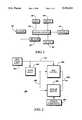
- FIG. 1is a block diagram of a selective call information display receiver.
- FIG. 2is a block diagram of the BIMOS integrated circuit system in accordance with the preferred embodiment.
- FIG. 3is a schematic diagram of the BIMOS electroluminescent display driver circuit.
- a battery 101 powered selective call receiveroperates to receive a signal via an antenna 102.
- the received signalis routed from the antenna 102 to the receiver 103.
- the receiver 103demodulates the received signals using conventional techniques and forwards the demodulated signal to the control circuitry 104, which decodes and recovers information contained within the received signal.
- the selective call receiverpresent at least a portion of the information, such as by a liquid crystal display 106, and signals the user via a sensible alert 107 that a message has been received. The user then views the information presented on the display 106 which is appropriately illuminated according to ambient lighting conditions.
- the receiver systems control circuitry 104can automatically enable backlighting of the display 106 in response to a predetermined level of ambient light detected.
- the displaymay also be illuminated by a user's manual intervention with the controls 105 which is then sensed by the control circuitry 104 illuminating the display 106.
- the receiver systemsuch that the battery 101 is a AA or AAA style which is readily available at their corner drug store. This allows the user to easily purchase and replace the battery 101 when a low cell condition is detected by the control circuitry 104.
- the control circuitry 104 shown in FIG. 1,may include, but is not restricted to, the following elements (not shown): signal multiplexing integrated circuits, a microcomputer, a digital memory coupled to the microcomputer, environmental sensing circuitry such as for light or temperature conditions, audio power amplifier circuitry, control interface circuitry, and display illumination driver circuitry. These elements are arranged in a manner which when assembled provides the display information receiver as requested by the customer.
- a variable MOS power supply 201provides bias to the MOS section 202 and the MOS power supply sense circuit 203.
- the bipolar power supply 204provides bias for the bipolar system 205 and can be used to generate the MOS power supply 201.
- the circuitry in the MOS section 202cannot operate because the MOS power supply 201 does not provide a high enough voltage, the voltage being denoted as V DD , to overcome the physical threshold of the MOS devices.
- the sense circuitry 203In a first state during a first time period, the sense circuitry 203 provides a signal 206 that disables the MOS section 202 and enables the bipolar section 205.
- the signal 206 from the sense circuitry 203changes level, initiating a second state and beginning a second time period in which the bipolar section 205 circuitry is disabled and the MOS section 202 circuitry is enabled. Note that the output of the MOS section 202 and the bipolar section 205 are coupled together, thus producing a continuous output signal 208 before and after the transition occurs from the bipolar section 205 to the MOS section 202.
- the sense circuitry 203can be a conventional comparator where the reference value is substantially equal to the value of voltage V DD required to power the MOS section 202.
- the comparator's outputchanges from a first to a second level, thus controlling the MOS 202 and bipolar 205 sections, respectively.
- This configurationinsures that the MOS section 202 will not operate until the voltage V DD from the MOS power supply 201 has reached a magnitude sufficient to properly power the MOS section 202.
- the bipolar means 317comprising transistor Q1 303, transistor Q2 304, and current source IREF 305
- the first sensing meanscomprising a sense circuit 313 for determining when an output voltage from the BIMOS electroluminescent display driver has reached a first predetermined value, the output voltage being the voltage V DD generated internal to the bridge circuit 312.
- the signal V DDon 301is held low (false).
- the signal V DDon 301is low (false) and a clock signal FCLK 302 having a frequency of 32 KHz for example, is applied at the base of transistor Q1 303.
- Transistor Q2 304acts as a current source mirroring the current of IREF 305 and providing a pull-up for the base of transistor Q1 303 during the absence of a signal at the base of transistor Q1 303.
- the coil L1 306which is coupled to the radio's BPLUS 307 (main power supply or battery), is grounded through the collector emitter junction of transistor Q1 303.
- This actioninduces a current in the coil L1 306 that is directed through diode D1 308 upon release of the base current applied to transistor Q1 303 by FCLK 302.
- the current directed through diode D1 308is coupled to the electroluminescent display panel 309 via the bridge circuit 312 and through the terminal EL1 310.
- Terminal EL2 311, connected to the electroluminescent display panel 309,is grounded by the bridge circuit 312. Since an electroluminescent display panel as an electronic load physically resembles a capacitor 309, the current will act to charge the capacitor to a voltage equal to the initial electroluminescent display panel voltage plus the product of the time duration and magnitude of the current pulse divided by the capacitance of the electroluminescent display panel.
- the charge on the capacitor or electroluminescent display panel 309increases and a corresponding increase in voltage is noted when measured across terminals EL1 310 and EL2 311 of the electroluminescent display panel 309.
- the voltage present at terminal EL1 310is sensed by high voltage limiting circuitry (not shown) internal to the bridge circuit 312 as well as by the sense circuit 313, and when the voltage reaches the predetermined threshold for V DD which is approximately 5 volts in magnitude, the sense circuit 313 forces the signal V DDon 301 high (true) and in response enables the first control means which enables and disables the MOS means 318 comprising MOS devices Ml 314, M2 315, and M3 316 and the bipolar means 317, respectively, in a complementary fashion.
- the signal V DDon 301when true turns on N channel MOS devices Ml 314 and M2 315. This action begins a second time period in which the bipolar means 317 is disabled and the MOS means 318 is enabled.
- MOS device M1 314grounds the base of transistor Q1 303 disabling the 32 KHz clock at its input.
- MOS device M2 315grounds the source of MOS device M3 316, thus enabling the application of a clock signal PCLK 319 having, for example, a frequency of 8 KHz, to the gate of MOS device M3 316, which in turn grounds the coil L1 306 at an 8 KHz rate providing current pulses through diode D1 308 to the electroluminescent display panel 309 for further charging.
- a second control meansresponsive to the second sensing means selects the direction of charge delivery to the electroluminescent display panel.
- terminal EL1 310is grounded and terminal EL2 311 is connected in series with diode D1 308.
- terminals EL1 310 and EL2 311are accomplished through the use of a conventional bridge configuration (not shown) within the bridge circuit 312 and the process described before for the charging of the electroluminescent display panel 309 is repeated in the opposite direction, thus producing a voltage magnitude difference approximately equal to twice the predetermined threshold for the maximum voltage applied the electroluminescent display panel 309 in a single direction.
- the single sided charging thresholdis set to be 70 volts above a reference potential
- the measured peak to peak voltage across the electroluminescent display panel terminals EL1 310 end EL2 311will be equal to two times seventy volts or 140 volts peak to peak.
- BIMOS technologyAnother advantage realized by using BIMOS technology is that when the circuit is constructed using strictly bipolar devices, the device geometries, isolation, and performance specifications required significantly increase the complexity and cost of the design.
- MOS devicesin the high voltage sections, their self-isolating design in terms of adjacent integrated circuit structures yields a significant performance advantage.
- Identical or similar circuitscannot be constructed using low power bipolar technology which operate with an input voltage substantially equal to 1.5 volts and produce and output voltage above forty volts peak to peak.
- This inventionmakes use of the low operating current and voltage requirements of bipolar devices in the startup region or portion of the operational sequence while developing the MOS power supply voltage from the electroluminescent display panel supply voltage.
- the use of MOS devices requiring little or no gate currentoptimizes the total efficiency of power conversion in the system and extends useful life of the receiver's power source.
Landscapes
- Engineering & Computer Science (AREA)
- Physics & Mathematics (AREA)
- Computer Hardware Design (AREA)
- General Physics & Mathematics (AREA)
- Theoretical Computer Science (AREA)
- Microelectronics & Electronic Packaging (AREA)
- Optics & Photonics (AREA)
- Control Of Indicators Other Than Cathode Ray Tubes (AREA)
- Control Of El Displays (AREA)
Abstract
Description
Claims (6)
Priority Applications (2)
| Application Number | Priority Date | Filing Date | Title |
|---|---|---|---|
| US07/520,894US5191321A (en) | 1990-05-09 | 1990-05-09 | Single cell bimos electroluminescent display driver |
| PCT/US1991/000865WO1991017537A1 (en) | 1990-05-09 | 1991-02-11 | Single cell bimos electroluminescent display driver |
Applications Claiming Priority (1)
| Application Number | Priority Date | Filing Date | Title |
|---|---|---|---|
| US07/520,894US5191321A (en) | 1990-05-09 | 1990-05-09 | Single cell bimos electroluminescent display driver |
Publications (1)
| Publication Number | Publication Date |
|---|---|
| US5191321Atrue US5191321A (en) | 1993-03-02 |
Family
ID=24074492
Family Applications (1)
| Application Number | Title | Priority Date | Filing Date |
|---|---|---|---|
| US07/520,894Expired - LifetimeUS5191321A (en) | 1990-05-09 | 1990-05-09 | Single cell bimos electroluminescent display driver |
Country Status (2)
| Country | Link |
|---|---|
| US (1) | US5191321A (en) |
| WO (1) | WO1991017537A1 (en) |
Cited By (6)
| Publication number | Priority date | Publication date | Assignee | Title |
|---|---|---|---|---|
| US5485172A (en)* | 1993-05-21 | 1996-01-16 | Sony Corporation | Automatic image regulating arrangement for head-mounted image display apparatus |
| US5736973A (en)* | 1995-11-01 | 1998-04-07 | Digital Ocean, Inc. | Integrated backlight display system for a personal digital assistant |
| EP1057089A4 (en)* | 1998-10-29 | 2002-04-10 | Durel Corp | Single inverter with dual boost |
| EP1300054A4 (en)* | 2000-05-18 | 2004-07-21 | Durel Corp | El driver with lamp discharge monitor |
| US20050017650A1 (en)* | 2003-07-24 | 2005-01-27 | Fryer Christopher James Newton | Control of electroluminescent displays |
| WO2005020200A1 (en)* | 2003-08-22 | 2005-03-03 | Pelikon Limited | Charge recovery for enhanced translator drive |
Families Citing this family (4)
| Publication number | Priority date | Publication date | Assignee | Title |
|---|---|---|---|---|
| US5519414A (en)* | 1993-02-19 | 1996-05-21 | Off World Laboratories, Inc. | Video display and driver apparatus and method |
| EP0655826B1 (en)* | 1993-11-29 | 1998-01-21 | STMicroelectronics S.r.l. | DC-DC boost converter for driving a capacitive load |
| US5463283A (en)* | 1994-05-24 | 1995-10-31 | Bkl, Inc. | Drive circuit for electroluminescent lamp |
| US5757351A (en)* | 1995-10-10 | 1998-05-26 | Off World Limited, Corp. | Electrode storage display addressing system and method |
Citations (13)
| Publication number | Priority date | Publication date | Assignee | Title |
|---|---|---|---|---|
| US4274014A (en)* | 1978-12-01 | 1981-06-16 | Rca Corporation | Switched current source for current limiting complementary symmetry inverter |
| US4553048A (en)* | 1984-02-22 | 1985-11-12 | Motorola, Inc. | Monolithically integrated thermal shut-down circuit including a well regulated current source |
| US4633141A (en)* | 1985-02-28 | 1986-12-30 | Motorola, Inc. | Low voltage power source power inverter for an electroluminescent drive |
| US4636665A (en)* | 1985-12-02 | 1987-01-13 | Motorola, Inc. | BIMOS memory sense amplifier |
| US4652932A (en)* | 1984-04-10 | 1987-03-24 | Citizen Watch Co., Ltd. | Liquid crystal display television receiver |
| US4695594A (en)* | 1986-08-27 | 1987-09-22 | General Electric Company | Modified flame retardant polyphenylene ether resins having improved foamability and molded articles made therefrom |
| US4865425A (en)* | 1985-12-03 | 1989-09-12 | Stanley Electric Co., Ltd. | Power source device for driving liquid crystal |
| US4904889A (en)* | 1987-12-03 | 1990-02-27 | Sgs-Thomson Microelectronics S.R.L. | Circuit for driving electronic devices with a low supply voltage |
| US4916338A (en)* | 1988-12-12 | 1990-04-10 | Tektronix, Inc. | FET buffer amplifier |
| US4943737A (en)* | 1989-10-13 | 1990-07-24 | Advanced Micro Devices, Inc. | BICMOS regulator which controls MOS transistor current |
| US4975694A (en)* | 1989-03-14 | 1990-12-04 | Motorola, Inc. | Paging receiver with variable color indicators |
| US4975692A (en)* | 1987-12-26 | 1990-12-04 | Canon Kabushiki Kaisha | Apparatus for driving electroluminescence panel |
| US4994694A (en)* | 1989-08-23 | 1991-02-19 | Tektronix, Inc. | Complementary composite PNP transistor |
Family Cites Families (1)
| Publication number | Priority date | Publication date | Assignee | Title |
|---|---|---|---|---|
| US4675594A (en)* | 1986-07-31 | 1987-06-23 | Honeywell Inc. | Voltage-to-current converter |
- 1990
- 1990-05-09USUS07/520,894patent/US5191321A/ennot_activeExpired - Lifetime
- 1991
- 1991-02-11WOPCT/US1991/000865patent/WO1991017537A1/enunknown
Patent Citations (13)
| Publication number | Priority date | Publication date | Assignee | Title |
|---|---|---|---|---|
| US4274014A (en)* | 1978-12-01 | 1981-06-16 | Rca Corporation | Switched current source for current limiting complementary symmetry inverter |
| US4553048A (en)* | 1984-02-22 | 1985-11-12 | Motorola, Inc. | Monolithically integrated thermal shut-down circuit including a well regulated current source |
| US4652932A (en)* | 1984-04-10 | 1987-03-24 | Citizen Watch Co., Ltd. | Liquid crystal display television receiver |
| US4633141A (en)* | 1985-02-28 | 1986-12-30 | Motorola, Inc. | Low voltage power source power inverter for an electroluminescent drive |
| US4636665A (en)* | 1985-12-02 | 1987-01-13 | Motorola, Inc. | BIMOS memory sense amplifier |
| US4865425A (en)* | 1985-12-03 | 1989-09-12 | Stanley Electric Co., Ltd. | Power source device for driving liquid crystal |
| US4695594A (en)* | 1986-08-27 | 1987-09-22 | General Electric Company | Modified flame retardant polyphenylene ether resins having improved foamability and molded articles made therefrom |
| US4904889A (en)* | 1987-12-03 | 1990-02-27 | Sgs-Thomson Microelectronics S.R.L. | Circuit for driving electronic devices with a low supply voltage |
| US4975692A (en)* | 1987-12-26 | 1990-12-04 | Canon Kabushiki Kaisha | Apparatus for driving electroluminescence panel |
| US4916338A (en)* | 1988-12-12 | 1990-04-10 | Tektronix, Inc. | FET buffer amplifier |
| US4975694A (en)* | 1989-03-14 | 1990-12-04 | Motorola, Inc. | Paging receiver with variable color indicators |
| US4994694A (en)* | 1989-08-23 | 1991-02-19 | Tektronix, Inc. | Complementary composite PNP transistor |
| US4943737A (en)* | 1989-10-13 | 1990-07-24 | Advanced Micro Devices, Inc. | BICMOS regulator which controls MOS transistor current |
Cited By (10)
| Publication number | Priority date | Publication date | Assignee | Title |
|---|---|---|---|---|
| US5485172A (en)* | 1993-05-21 | 1996-01-16 | Sony Corporation | Automatic image regulating arrangement for head-mounted image display apparatus |
| US5736973A (en)* | 1995-11-01 | 1998-04-07 | Digital Ocean, Inc. | Integrated backlight display system for a personal digital assistant |
| EP1057089A4 (en)* | 1998-10-29 | 2002-04-10 | Durel Corp | Single inverter with dual boost |
| EP1300054A4 (en)* | 2000-05-18 | 2004-07-21 | Durel Corp | El driver with lamp discharge monitor |
| US20050017650A1 (en)* | 2003-07-24 | 2005-01-27 | Fryer Christopher James Newton | Control of electroluminescent displays |
| US7119493B2 (en)* | 2003-07-24 | 2006-10-10 | Pelikon Limited | Control of electroluminescent displays |
| WO2005020200A1 (en)* | 2003-08-22 | 2005-03-03 | Pelikon Limited | Charge recovery for enhanced translator drive |
| US20070139301A1 (en)* | 2003-08-22 | 2007-06-21 | Fryer Christopher J N | Charge recovery for enhanced transistor drive |
| CN100527201C (en)* | 2003-08-22 | 2009-08-12 | 佩利康有限公司 | Charge recovery for enhanced translator drive |
| US8111214B2 (en) | 2003-08-22 | 2012-02-07 | Mflex Uk Limited | Charge recovery for enhanced transistor drive |
Also Published As
| Publication number | Publication date |
|---|---|
| WO1991017537A1 (en) | 1991-11-14 |
Similar Documents
| Publication | Publication Date | Title |
|---|---|---|
| US4634953A (en) | Electronic equipment with solar cell | |
| US5982104A (en) | Driver for capacitive light-emitting device with degradation compensated brightness control | |
| US5191321A (en) | Single cell bimos electroluminescent display driver | |
| US4736121A (en) | Charge pump circuit for driving N-channel MOS transistors | |
| US5914589A (en) | Voltage boosting circuit for high-potential-side MOS switching transistor | |
| US20080224638A1 (en) | Key module having light-indicating functionality and a method for controlling the same | |
| US5120991A (en) | Driver circuit for converting a cmos level signal to a high-voltage level | |
| US20030020676A1 (en) | Fast-working LCD residual display suppression circuit and a method thereto | |
| US5745775A (en) | Remotely adjustable price display module | |
| US5381044A (en) | Bootstrap circuit for driving a power MOS transistor | |
| US5939840A (en) | Liquid crystal back light illuminating device and liquid crystal display device | |
| US4727261A (en) | Multiple power FET vehicle lamp switch arrangement with charge pump sharing | |
| KR950008867B1 (en) | Paging receiver with alternating speakers and LEDs on incoming call | |
| JP2517709Y2 (en) | Wireless selective call receiver | |
| US4006583A (en) | Electronic display device for timepiece and the like | |
| US5644194A (en) | Circuit for controlling an indicator light to turn off slowly | |
| US6252786B1 (en) | Electric power control method and circuit with controlled fadeout of power consumption | |
| US4435089A (en) | Power circuit for an electronic timepiece | |
| JP2000012215A (en) | El drive circuit system | |
| US4051664A (en) | Drive circuit of light emitting means for liquid crystal electronic watch | |
| WO1992005536A1 (en) | Electroluminescent panel driver with efficient start-up | |
| JPS609752Y2 (en) | car electric clock | |
| US20060132478A1 (en) | High-potential output stage | |
| KR960004405Y1 (en) | Power restart circuit | |
| JPH04285999A (en) | Driving circuit for piezoelectric buzzer |
Legal Events
| Date | Code | Title | Description |
|---|---|---|---|
| AS | Assignment | Owner name:MOTOROLA, INC., ILLINOIS Free format text:ASSIGNMENT OF ASSIGNORS INTEREST.;ASSIGNORS:HEROLD, BARRY W.;MC LAUGHLIN, KEVIN;REEL/FRAME:005299/0766 Effective date:19900504 | |
| STCF | Information on status: patent grant | Free format text:PATENTED CASE | |
| CC | Certificate of correction | ||
| FPAY | Fee payment | Year of fee payment:4 | |
| FPAY | Fee payment | Year of fee payment:8 | |
| AS | Assignment | Owner name:FREESCALE SEMICONDUCTOR, INC., TEXAS Free format text:ASSIGNMENT OF ASSIGNORS INTEREST;ASSIGNOR:MOTOROLA, INC.;REEL/FRAME:015698/0657 Effective date:20040404 Owner name:FREESCALE SEMICONDUCTOR, INC.,TEXAS Free format text:ASSIGNMENT OF ASSIGNORS INTEREST;ASSIGNOR:MOTOROLA, INC.;REEL/FRAME:015698/0657 Effective date:20040404 | |
| FPAY | Fee payment | Year of fee payment:12 | |
| AS | Assignment | Owner name:CITIBANK, N.A. AS COLLATERAL AGENT, NEW YORK Free format text:SECURITY AGREEMENT;ASSIGNORS:FREESCALE SEMICONDUCTOR, INC.;FREESCALE ACQUISITION CORPORATION;FREESCALE ACQUISITION HOLDINGS CORP.;AND OTHERS;REEL/FRAME:018855/0129 Effective date:20061201 Owner name:CITIBANK, N.A. AS COLLATERAL AGENT,NEW YORK Free format text:SECURITY AGREEMENT;ASSIGNORS:FREESCALE SEMICONDUCTOR, INC.;FREESCALE ACQUISITION CORPORATION;FREESCALE ACQUISITION HOLDINGS CORP.;AND OTHERS;REEL/FRAME:018855/0129 Effective date:20061201 | |
| AS | Assignment | Owner name:CITIBANK, N.A., AS COLLATERAL AGENT,NEW YORK Free format text:SECURITY AGREEMENT;ASSIGNOR:FREESCALE SEMICONDUCTOR, INC.;REEL/FRAME:024397/0001 Effective date:20100413 Owner name:CITIBANK, N.A., AS COLLATERAL AGENT, NEW YORK Free format text:SECURITY AGREEMENT;ASSIGNOR:FREESCALE SEMICONDUCTOR, INC.;REEL/FRAME:024397/0001 Effective date:20100413 | |
| AS | Assignment | Owner name:FREESCALE SEMICONDUCTOR, INC., TEXAS Free format text:PATENT RELEASE;ASSIGNOR:CITIBANK, N.A., AS COLLATERAL AGENT;REEL/FRAME:037354/0225 Effective date:20151207 Owner name:FREESCALE SEMICONDUCTOR, INC., TEXAS Free format text:PATENT RELEASE;ASSIGNOR:CITIBANK, N.A., AS COLLATERAL AGENT;REEL/FRAME:037356/0143 Effective date:20151207 Owner name:FREESCALE SEMICONDUCTOR, INC., TEXAS Free format text:PATENT RELEASE;ASSIGNOR:CITIBANK, N.A., AS COLLATERAL AGENT;REEL/FRAME:037356/0553 Effective date:20151207 |