US5185602A - Method and apparatus for producing perception of high quality grayscale shading on digitally commanded displays - Google Patents
Method and apparatus for producing perception of high quality grayscale shading on digitally commanded displaysDownload PDFInfo
- Publication number
- US5185602A US5185602AUS07/335,622US33562289AUS5185602AUS 5185602 AUS5185602 AUS 5185602AUS 33562289 AUS33562289 AUS 33562289AUS 5185602 AUS5185602 AUS 5185602A
- Authority
- US
- United States
- Prior art keywords
- brightness
- pixels
- phase
- setting
- pixel
- Prior art date
- Legal status (The legal status is an assumption and is not a legal conclusion. Google has not performed a legal analysis and makes no representation as to the accuracy of the status listed.)
- Expired - Lifetime
Links
- 230000008447perceptionEffects0.000titleclaimsabstractdescription20
- 238000000034methodMethods0.000titleclaimsdescription52
- 239000011159matrix materialSubstances0.000claimsdescription35
- 230000001788irregularEffects0.000claimsdescription9
- 230000004044responseEffects0.000claimsdescription9
- 230000010354integrationEffects0.000claimsdescription3
- 238000004519manufacturing processMethods0.000claimsdescription3
- 238000009826distributionMethods0.000claimsdescription2
- 210000004027cellAnatomy0.000claims7
- 238000000059patterningMethods0.000claims4
- 210000002325somatostatin-secreting cellAnatomy0.000claims4
- 238000004513sizingMethods0.000claims1
- 206010047571Visual impairmentDiseases0.000abstractdescription10
- 239000004973liquid crystal related substanceSubstances0.000description22
- 230000000694effectsEffects0.000description13
- 238000011068loading methodMethods0.000description11
- 238000010586diagramMethods0.000description10
- 230000006870functionEffects0.000description8
- 238000003491arrayMethods0.000description7
- 230000005684electric fieldEffects0.000description6
- 239000000463materialSubstances0.000description6
- 239000003990capacitorSubstances0.000description5
- 230000000007visual effectEffects0.000description4
- 230000003213activating effectEffects0.000description3
- 238000004458analytical methodMethods0.000description3
- 230000006399behaviorEffects0.000description3
- 230000000295complement effectEffects0.000description3
- 230000001186cumulative effectEffects0.000description3
- 238000005516engineering processMethods0.000description3
- 230000000737periodic effectEffects0.000description3
- 230000002123temporal effectEffects0.000description3
- 230000015572biosynthetic processEffects0.000description2
- 230000008901benefitEffects0.000description1
- 230000008859changeEffects0.000description1
- 239000002131composite materialSubstances0.000description1
- 238000005094computer simulationMethods0.000description1
- 239000004020conductorSubstances0.000description1
- 230000003111delayed effectEffects0.000description1
- 238000010894electron beam technologyMethods0.000description1
- 230000008030eliminationEffects0.000description1
- 238000003379elimination reactionMethods0.000description1
- 230000006872improvementEffects0.000description1
- 230000007246mechanismEffects0.000description1
- 230000002093peripheral effectEffects0.000description1
- 230000008569processEffects0.000description1
- 230000002441reversible effectEffects0.000description1
- 230000001360synchronised effectEffects0.000description1
- 230000007704transitionEffects0.000description1
Images


Classifications
- H—ELECTRICITY
- H04—ELECTRIC COMMUNICATION TECHNIQUE
- H04N—PICTORIAL COMMUNICATION, e.g. TELEVISION
- H04N3/00—Scanning details of television systems; Combination thereof with generation of supply voltages
- H04N3/10—Scanning details of television systems; Combination thereof with generation of supply voltages by means not exclusively optical-mechanical
- H04N3/12—Scanning details of television systems; Combination thereof with generation of supply voltages by means not exclusively optical-mechanical by switched stationary formation of lamps, photocells or light relays
- H04N3/127—Scanning details of television systems; Combination thereof with generation of supply voltages by means not exclusively optical-mechanical by switched stationary formation of lamps, photocells or light relays using liquid crystals
- G—PHYSICS
- G09—EDUCATION; CRYPTOGRAPHY; DISPLAY; ADVERTISING; SEALS
- G09G—ARRANGEMENTS OR CIRCUITS FOR CONTROL OF INDICATING DEVICES USING STATIC MEANS TO PRESENT VARIABLE INFORMATION
- G09G3/00—Control arrangements or circuits, of interest only in connection with visual indicators other than cathode-ray tubes
- G09G3/20—Control arrangements or circuits, of interest only in connection with visual indicators other than cathode-ray tubes for presentation of an assembly of a number of characters, e.g. a page, by composing the assembly by combination of individual elements arranged in a matrix no fixed position being assigned to or needed to be assigned to the individual characters or partial characters
- G09G3/2003—Display of colours
- G—PHYSICS
- G09—EDUCATION; CRYPTOGRAPHY; DISPLAY; ADVERTISING; SEALS
- G09G—ARRANGEMENTS OR CIRCUITS FOR CONTROL OF INDICATING DEVICES USING STATIC MEANS TO PRESENT VARIABLE INFORMATION
- G09G3/00—Control arrangements or circuits, of interest only in connection with visual indicators other than cathode-ray tubes
- G09G3/20—Control arrangements or circuits, of interest only in connection with visual indicators other than cathode-ray tubes for presentation of an assembly of a number of characters, e.g. a page, by composing the assembly by combination of individual elements arranged in a matrix no fixed position being assigned to or needed to be assigned to the individual characters or partial characters
- G09G3/2007—Display of intermediate tones
- G09G3/2044—Display of intermediate tones using dithering
- G09G3/2051—Display of intermediate tones using dithering with use of a spatial dither pattern
- G—PHYSICS
- G09—EDUCATION; CRYPTOGRAPHY; DISPLAY; ADVERTISING; SEALS
- G09G—ARRANGEMENTS OR CIRCUITS FOR CONTROL OF INDICATING DEVICES USING STATIC MEANS TO PRESENT VARIABLE INFORMATION
- G09G3/00—Control arrangements or circuits, of interest only in connection with visual indicators other than cathode-ray tubes
- G09G3/20—Control arrangements or circuits, of interest only in connection with visual indicators other than cathode-ray tubes for presentation of an assembly of a number of characters, e.g. a page, by composing the assembly by combination of individual elements arranged in a matrix no fixed position being assigned to or needed to be assigned to the individual characters or partial characters
- G09G3/2092—Details of a display terminals using a flat panel, the details relating to the control arrangement of the display terminal and to the interfaces thereto
- G—PHYSICS
- G09—EDUCATION; CRYPTOGRAPHY; DISPLAY; ADVERTISING; SEALS
- G09G—ARRANGEMENTS OR CIRCUITS FOR CONTROL OF INDICATING DEVICES USING STATIC MEANS TO PRESENT VARIABLE INFORMATION
- G09G3/00—Control arrangements or circuits, of interest only in connection with visual indicators other than cathode-ray tubes
- G09G3/20—Control arrangements or circuits, of interest only in connection with visual indicators other than cathode-ray tubes for presentation of an assembly of a number of characters, e.g. a page, by composing the assembly by combination of individual elements arranged in a matrix no fixed position being assigned to or needed to be assigned to the individual characters or partial characters
- G09G3/34—Control arrangements or circuits, of interest only in connection with visual indicators other than cathode-ray tubes for presentation of an assembly of a number of characters, e.g. a page, by composing the assembly by combination of individual elements arranged in a matrix no fixed position being assigned to or needed to be assigned to the individual characters or partial characters by control of light from an independent source
- G09G3/36—Control arrangements or circuits, of interest only in connection with visual indicators other than cathode-ray tubes for presentation of an assembly of a number of characters, e.g. a page, by composing the assembly by combination of individual elements arranged in a matrix no fixed position being assigned to or needed to be assigned to the individual characters or partial characters by control of light from an independent source using liquid crystals
- G09G3/3611—Control of matrices with row and column drivers
- G—PHYSICS
- G09—EDUCATION; CRYPTOGRAPHY; DISPLAY; ADVERTISING; SEALS
- G09G—ARRANGEMENTS OR CIRCUITS FOR CONTROL OF INDICATING DEVICES USING STATIC MEANS TO PRESENT VARIABLE INFORMATION
- G09G2320/00—Control of display operating conditions
- G09G2320/02—Improving the quality of display appearance
- G09G2320/0247—Flicker reduction other than flicker reduction circuits used for single beam cathode-ray tubes
- G—PHYSICS
- G09—EDUCATION; CRYPTOGRAPHY; DISPLAY; ADVERTISING; SEALS
- G09G—ARRANGEMENTS OR CIRCUITS FOR CONTROL OF INDICATING DEVICES USING STATIC MEANS TO PRESENT VARIABLE INFORMATION
- G09G2320/00—Control of display operating conditions
- G09G2320/02—Improving the quality of display appearance
- G09G2320/0261—Improving the quality of display appearance in the context of movement of objects on the screen or movement of the observer relative to the screen
- G—PHYSICS
- G09—EDUCATION; CRYPTOGRAPHY; DISPLAY; ADVERTISING; SEALS
- G09G—ARRANGEMENTS OR CIRCUITS FOR CONTROL OF INDICATING DEVICES USING STATIC MEANS TO PRESENT VARIABLE INFORMATION
- G09G2320/00—Control of display operating conditions
- G09G2320/02—Improving the quality of display appearance
- G09G2320/0266—Reduction of sub-frame artefacts
- G—PHYSICS
- G09—EDUCATION; CRYPTOGRAPHY; DISPLAY; ADVERTISING; SEALS
- G09G—ARRANGEMENTS OR CIRCUITS FOR CONTROL OF INDICATING DEVICES USING STATIC MEANS TO PRESENT VARIABLE INFORMATION
- G09G2320/00—Control of display operating conditions
- G09G2320/02—Improving the quality of display appearance
- G09G2320/0271—Adjustment of the gradation levels within the range of the gradation scale, e.g. by redistribution or clipping
- G09G2320/0276—Adjustment of the gradation levels within the range of the gradation scale, e.g. by redistribution or clipping for the purpose of adaptation to the characteristics of a display device, i.e. gamma correction
- G—PHYSICS
- G09—EDUCATION; CRYPTOGRAPHY; DISPLAY; ADVERTISING; SEALS
- G09G—ARRANGEMENTS OR CIRCUITS FOR CONTROL OF INDICATING DEVICES USING STATIC MEANS TO PRESENT VARIABLE INFORMATION
- G09G2360/00—Aspects of the architecture of display systems
- G09G2360/18—Use of a frame buffer in a display terminal, inclusive of the display panel
- G—PHYSICS
- G09—EDUCATION; CRYPTOGRAPHY; DISPLAY; ADVERTISING; SEALS
- G09G—ARRANGEMENTS OR CIRCUITS FOR CONTROL OF INDICATING DEVICES USING STATIC MEANS TO PRESENT VARIABLE INFORMATION
- G09G3/00—Control arrangements or circuits, of interest only in connection with visual indicators other than cathode-ray tubes
- G09G3/20—Control arrangements or circuits, of interest only in connection with visual indicators other than cathode-ray tubes for presentation of an assembly of a number of characters, e.g. a page, by composing the assembly by combination of individual elements arranged in a matrix no fixed position being assigned to or needed to be assigned to the individual characters or partial characters
- G09G3/2007—Display of intermediate tones
- G09G3/2018—Display of intermediate tones by time modulation using two or more time intervals
- G09G3/2022—Display of intermediate tones by time modulation using two or more time intervals using sub-frames
- G09G3/2025—Display of intermediate tones by time modulation using two or more time intervals using sub-frames the sub-frames having all the same time duration
Definitions
- the present inventionis directed to a method and apparatus for producing the perception of grayscale shading on digitally controlled displays.
- the inventionis more specifically directed to a method and apparatus for generating the perception of many different brightness levels by digitally commanding the pixels of multiplexed liquid crystal displays towards either full brightness or complete darkness at appropriate times.
- Grayscale shadingcan be generated on the screen of a conventional cathode ray tube (CRT) by varying an analog brightness control voltage at the grid electrode of the tube while an electron beam of the CRT is swept across different pixel positions of a display line.
- CTRcathode ray tube
- the same grayscale shading techniquedoes not lend itself to digitally commanded displays such as multiplexed liquid crystal displays (LCD's), light emitting diode (LED) displays or plasma displays wherein individual pixels (discrete light source regions including emissive, transmissive and reflective types) can be commanded to switch towards only one of two brightness levels, ON or OFF (i.e., white or black).
- Such digital displaysgenerally lack an analog control electrode equivalent to the grid electrode of a CRT and thus they do not have a direct means independent of their power lines for commanding a pixel towards an intermediate brightness level between black and white.
- Multiplexed displaystypically have only two electrodes provided at each pixel area for addressing a pixel area and energizing the pixel area to either produce the appearance of a fully lit (white) pixel or to produce the appearance of a fully darkened (black) pixel. Since an analog means for controlling brightness level is not available on many types of digital displays including raster-scan multiplexed displays, alternative digital techniques have been proposed for giving a viewer the perception of grayscale shading.
- One of the proposed alternative techniquesis a so-called "pulse-width modulation” scheme wherein the width of pixel energizing pulses is modulated between wide and narrow values to create a grayscale effect.
- Another techniqueis a so-called “frame-rate duty cycle modulation” scheme wherein the duration between energizing pulses of fixed width is varied between long and short to create a grayscale effect.
- a third proposed approachis to switch from the use of "time multiplexed" digital displays (which are commonly employed in laptop computers) to so-called “active matrix” display panels, the latter panels being ones which have active pixel-driving electronics defined at the location of each pixel, and to form a three-terminal analog-controllable display element out of such an active-matrix topology for continuously energizing each pixel discretely to a desired level of brightness.
- pulse-width modulation schemeis adopted, substantial redesign of already available display-driving electronics may be required to produce pixel energizing pulses of variable width and the cost of such new electronics may be significantly higher than that of the already-available drive electronics. Additionally, undesirable crosstalk between densely packed circuits may be created by employing the pulse-width modulation scheme since a high frequency harmonic content is typically associated with the relatively narrow pulses that might be produced by the latter technique. Because changes to the already proven technology of conventional panel-driving electronics are generally undesirable, the pulse-width modulation scheme is not presently acceptable within the industry.
- the frame-rate duty cycle modulation methodappears to be more acceptable to the industry at the current time, but this latter method is not without problems.
- Display elements based on light emitting diode (LED), liquid crystal (LCD), electro-luminescent (EL), plasma or other technologiestypically require periodic application of refresh energy in order to retain their appearance of being lit or unlit (bright or dark).
- the frame-rate duty cycle modulation techniqueoperates by extending the time between pixel energizing pulses.
- the duration between energizing pulsesis reduced substantially below a brightness integrating period associated with the human eye (i.e., substantially below one sixtieth of a second) in order to create a grayscale effect, a noticeable and undesirable perception of flickering within the display image may be created, particularly when a large number of pixels are being simultaneously commanded towards one of the ON and OFF states.
- grayscaleis intended to be applied here to not only monochromatic displays but also to color displays wherein the brightness (occularly perceived luminance) of a colored region is to be varied across a predetermined intensity range.
- the inventionis not limited to any one display technology and should be applicable to all types of displays wherein pixels are discretely commanded towards one or the other of a bright and dark level.
- grayscalingis effected by providing at least six different waveforms (brightness-setting waveforms), each having at least five ON/OFF command bits which are sequentially produced over a predetermined phase-scattering period.
- the phase-scattering periodis preferably selected to be equal to D times a predetermined frame period, where D is an integer associated with a D-by-D square phase-placement pattern (matrix).
- the side dimension D of the phase-placement patternis preferably selected to enable tiling of a plane with irregular rectangles of dimensions a-by-b, where a is not equal to b, while simultaneously filling the plane with a checkerboard pattern formed of D-by-D squares.
- Pixel energizing commands which are to occur during a common time spanare preferably positioned at opposed diagonal corners of the rectangles to maximize distance between simultaneously energized pixel locations and to spread the load on column and row drivers which are energizing the pixel locations.
- the at least six brightness-setting waveformsmay be used for not only commanding display pixels to appear either fully ON or OFF (white or black) but also for creating the perception of intermediate brightness levels distributed across the range between full ON or OFF.
- the first of the six digital waveformshas a first average duty cycle (averaged over the predetermined phase-scattering period) which is associated with a maximum brightness level.
- the sixth digital waveformhas a corresponding sixth average duty cycle (taken over the predetermined phase-scattering period) which is associated with a minimum brightness level.
- the second through fifth digital waveformsrespectively have second through fifth, different average duty cycles (again taken over the predetermined phase-scattering period) which are preferably associated with different levels of apparent brightness spaced in a generally periodic manner (approximately equally spaced) between the maximum and minimum brightness levels.
- the ON command bits of any one brightness-setting waveformare preferably equally spaced apart from each other over time and the OFF command bits of each waveform are likewise preferably spaced equally apart from one another over time so that low frequency components of each waveform are suppressed relative to high frequency components of the same waveform.
- the first and sixth digital waveformsare preferably paired to have ON/OFF command bits which are binary complements of one another so that the command bits of the sixth digital waveform may be produced by performing a sequential binary NOT operation on the ON/OFF command bits of the first digital waveform.
- the second and fifth digital waveformsare preferably paired to be binary complements of one another so that the fifth digital waveform may be produced by performing a binary NOT operation on the bits of the second digital waveform.
- the third and fourth digital waveformsare also preferably paired as binary complements of each other. This preferred use of binary complementable waveforms will be referred to later within the specification as "grayscale mirroring".
- digital information representing approximately half of the six or more digital waveformsis stored in a memory device (i.e. a waveform ROM) and the complementary others of the six or more digital waveforms are not represented by stored data but rather reproduced by performing a binary NOT operation on the data of the stored waveforms.
- a memory devicei.e. a waveform ROM
- phase-shifted versions of at least one of the second and fifth digital waveformsare applied to adjacent pixel areas of a matrixed display at different times (i.e., in different display "frames").
- Phase selectionis determined in accordance with both the row and column numbers which designate the location in the matrix of the pixel that is to be driven by the at least one waveform.
- a predetermined phase selection arrayis stored in memory and phase selection values are dynamically read from memory as a display is being scanned to determine which of the ON/OFF command bits of a preselected brightness-setting waveform is to be transmitted to a pixel in a specific row and column during a particular frame cycle.
- the output loadings on row and column drivers of a multiplexed display panelare balanced by distributing the phases of at least one of the digital waveforms in accordance with a square phase-placement pattern.
- the number of distinguishable brightness levels to be displayed(which is the same as the number of utilized brightness-setting waveforms) is preferably chosen to be less than the side dimension D of the D ⁇ D placement pattern even though the D ⁇ D pattern can support D+1 or more brightness levels (i.e., only 16 levels are chosen for a 17 ⁇ 17 phase-placement pattern capable of supporting as many as 18 levels).
- one of a plurality of predetermined phase-placement patternsis dynamically selected depending on the state of previously displayed pixels.
- 2 ⁇ 2 stippling patternseach having four pixels with pairs thereof operating at two different brightness levels other than black or white, are formed to create the perception of grayscale levels between those realizable by the individual pixels alone.
- the left to right ordering of the different brightness levelsis preferably alternated in adjacent horizontal lines of the display to prevent the formation of vertical gray streaks.
- FIG. 1Ais a block diagram showing the structure of a conventional digital display.
- FIG. 1Bis a cross-sectional view of a liquid crystal display panel.
- FIG. 1Cis a top view of the panel shown in FIG. 1B for explaining electrical and visual crosstalk between adjacent pixels.
- FIG. 2Ashows the waveform of a frame rate duty cycle modulated waveform for controlling the apparent brightness of a pixel.
- FIG. 2Bis a graph illustrating the cumulative response of liquid crystal display panels over multiple frame periods.
- FIG. 2Cis a schematic diagram of a first order model for explaining the time-space integrating behavior of adjacent liquid crystal display elements and the time-space integrating behavior of a human eye which is viewing the display elements.
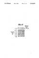
- FIG. 3Ais a schematic diagram of a previously proposed apparatus for creating a three level brightness effect in a liquid crystal display panel.
- FIG. 3Billustrates an elemental 2 ⁇ 2 phase-placement pattern which may be associated with the embodiment shown in FIG. 3A.
- FIG. 3Cillustrates a display area which is tiled by the elemental phase-placement pattern of FIG. 3B.
- FIG. 4Aillustrates a set of brightness-setting waveforms capable of producing a grayscale effect having four brightness levels.
- FIG. 4Billustrates a possible phase-placement pattern for the brightness-setting waveforms illustrated in FIG. 4A.
- FIG. 4Cillustrates how visual disturbances can be created by the phase-placement pattern of FIG. 4B.
- FIG. 4Dillustrates a set of brightness-setting waveforms wherein the next to lowest brightness-setting waveform has four phases.
- FIG. 4Eillustrates a possible phase-placement pattern for the brightness-setting waveforms illustrated in FIG. 4D.
- FIG. 4Fillustrates how visual disturbances can be created by the phase-placement pattern of FIG. 4E.
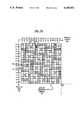
- FIG. 5Ashows a possible 4 ⁇ 4 phase-placement pattern for a brightness-setting waveform having 16 different phases.
- FIG. 5Billustrates how unbalanced loading of row and column drivers may occur using the 4 ⁇ 4 phase-placement pattern illustrated in FIG. 5A.
- FIG. 6Aillustrates a 5 ⁇ 5 phase-placement matrix in accordance with the present invention.
- FIG. 6Billustrates two frames in time of a display area which is tiled by the 5 ⁇ 5 phase-placement matrix shown in FIG. 6A.
- FIG. 6Cillustrates a fill pattern for the 5 ⁇ 5 phase-placement matrix of FIG. 6A.
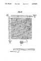
- FIG. 7Aillustrates a 17 ⁇ 17 phase-placement pattern in accordance with the invention.
- FIG. 7Billustrates a preferred distance jump to be made by the pixel energizing points of sequential frames.
- FIG. 7Cillustrates a first ordering of phases within the 17 ⁇ 17 phase-placement pattern.
- FIG. 7Dillustrates a second ordering of phases within the 17 ⁇ 17 phase placement pattern.
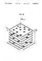
- FIG. 7Eis a three dimensional conceptualization of multiple frames attacked along a time axis.
- FIG. 8shows a set of brightness-setting waveforms in accordance with the invention.
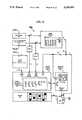
- FIG. 9is a block diagram of a first brightness control system in accordance with the invention.
- FIG. 10is a block diagram of a second brightness control system in accordance with the invention.
- FIG. 11is a schematic diagram of a brightness control system in accordance with the invention.
- FIG. 1is a block diagram of a conventional digitally controlled display system 10.
- the display system 10comprises a raster-scan compatible type of multiplexed liquid crystal (LCD) panel unit 11 in which there is provided a two-dimensional matrix 12 of pixel regions 12a, each of which is uniquely addressable by orthogonal row and column electrodes, 12b and 12c.
- the row and column electrodes 12b and 12care respectively placed as densely packed parallel conductors on the top and bottom surfaces of a display panel (not shown) with a preselected liquid crystal material 12d (FIG. 1B) being sandwiched between the top and bottom electrodes, 12b and 12c.
- LCDliquid crystal
- the top electrodes (i.e., 12b) and top portion of the display panel (not shown)are preferably made of transparent layers.
- An electric field 12e (FIG. 1B)is applied to the liquid crystal material 12d of a preselected pixel area 12a (FIG. 1A) by activating a preselected one of a plurality of line drivers 14 coupled to the row electrodes 12b and simultaneously activating one or more of a plurality of column drivers 16 coupled to the column electrodes 12c.
- Positive and negative (ground) power terminals of the row and column drivers, 14 and 16are usually connected to common high and low voltage rails (+V and -V).
- a composite imagemay be formed by sequentially activating the rows (i.e., R1-R6 of FIG. 1) of the display matrix 12 one row at a time in time multiplexed fashion and transmitting binary video data to the pixel areas 12a of the selected row (Rx) through the column drivers 16.
- the column drivers 16receive binary video data in prestored parallel fashion from a line register 26.
- the binary video dataoriginates in an image memory 20 which is addressed by a synchronous address counter 21.
- the address counter 21is clocked by a high frequency dot clock (pixel clock) 23.
- Video datais output from the image memory 20 along a four-bit wide serial bus 24 to a shift register 22 also clocked by the dot clock 23.
- the shift register 22transforms the 4-bit wide serial data stream 24 of video bit data into a wider parallel data format 25 and this parallel data 25 is loaded into the line register 26 when the latter register 26 is strobed by a horizontal synchronization pulse (line clock) 27.
- the horizontal synchronization pulse 27also clocks a one-of-N line selector 18 which activates a desired one of the plural row drivers 14 to place a low potential (-V) on its corresponding row electrode 12b.
- a vertical sync pulse (frame start pulse) 28is applied to a reset terminal of the line selector 18 at the end of each display frame in order to restart the row scanning from the top line (R1) of the display matrix 12 towards a preselected bottom line (R6).
- the display matrix 12is organized as a unit (display segment) of 480 to 640 columns by 200 to 240 rows and all the rows are scanned at a rate of approximately 50 to 120 Hz (usually V-synch pulses 28 are generated sixty times a second).
- the H-synch clock 27typically operates at 10 KHz to 30 KHz and the dot clock 23 operates at roughly 6 MHz.
- display segmentsare stacked one on top of another and each display segment is refreshed at a frame rate of approximately 50 to 120 Hz.
- FIG. 1Bwhich shows a cross-sectional view of a liquid crystal display panel
- the electric field 12e emanating from plural column electrodes 12ctends to enlarge in width as it extends to the orthogonal row electrode 12b to the orthogonal row electrode 12b above the plural column electrodes 12c.
- the electric field 12e of a first turned on column electrode 12cit is possible for the electric field 12e of a first turned on column electrode 12c to encroach on an adjacent region of liquid crystal material 12d which is to be controlled by an adjacent column electrode 12c.
- the possibility of overlap between electrical fields of adjacent pixel areas 12ais denoted by the overlapping boundaries of rounded rectangles 12f.
- the physical overlap of the top 12b and bottom 12c electrodesis denoted by the hatched square areas marked as regions 12a.
- a central one of the nine pixel areas 12a shown in FIG. 1Cis left unhatched to show how the effective area and/or apparent brightness of an unlit pixel can be reduced by the encroachment of electrical field peripheries 12f of surrounding lit pixels.
- the brightness of a pixel area 12a in a liquid crystal displaycan be incremented to a higher brightness level by applying a plurality of charging pulses 31 across its row and column electrodes, 12b and 12c, and the brightness of the pixel area 12a can be decremented towards a lower brightness level by applying one or more discharge pulses 32 across its respective electrodes.
- the bits (i.e. "1101") of a video data string 30 supplied by a userdetermines whether a charge or discharge pulse will be applied. These bits 30 are supplied at pixel strobing times T 0 , T 1 , T 2 , T 3 , etc.
- a one-time scanning of all the pixels in the display matrix 12 on a sequential line by line basisis referred to in the industry as a "frame refresh", "frame cycle”, or “frame period”.
- framesare refreshed at the rate of approximately 50 to 120 times per second (usually 60 Hz).
- Only one charge pulse 31 or discharge pulse 32is applied to each individual pixel area 12a during a single frame refresh cycle (a frame period, FP). If a series of charge 31 and discharge 32 command pulses are to be applied to a single pixel area for achieving a desired level of brightness based on average duty-cycle, such a series is normally applied over the course of many frame periods (i.e., four or more frame cycles).
- the typical response P R time of a liquid crystal displaycan be on the order of 100 to 350 milliseconds (time for incrementing or decrementing the brightness of a pixel across a range between 10% and 90% of maximum brightness).
- a large number (i.e. 21) of frame refresh cyclesmay be required to raise the brightness level of a single pixel area 12a from a relatively low brightness level (i.e. 10%) to a relatively high brightness level (i.e. 90%) and to conversely decrease the brightness level over a same span.
- Periodic refreshingis required to retain a desired level of brightness.
- FIG. 2Cthere is shown a schematic diagram of a first order model for explaining the perceived behavior of adjacent pixel areas 12a in a liquid crystal display (LCD).
- Each pixel areamay be modeled by a finite capacitor C D across which there is placed a bleed-resistor R b of relatively high resistance.
- the luminance (photometric) of the pixel area 12a(represented by voltage across the display capacitance C D ) may be incremented by transmitting charge pulses 31 through a charge resistor R c and may be decremented by applying discharge pulses 32 through a discharge resistance R d .
- Electrical crosstalk from the fields 12f of adjacent pixelscan enter the integrating function (capacitor) C D of the pixel through resistor R a .
- the model of FIG. 2Cis based on the idea that the reorientation of liquid crystal molecules occurs as a cumulative effect and that such molecules have a natural tendency to relax (discharge through bleed resistor R b ) into a natural state if not periodically refreshed.
- the level of brightness perceived by the human eyetends to be an integrated function over time of the brightness level transmitted by each individual pixel area 12a as well as an integrated function over space of light received from adjacent pixels.
- the model of FIG. 2Cincludes a second order integrating circuit having resistor R E1 and capacitor C E1 for representing the delayed cumulative response of the human eye to a first display element (pixel) and a second resistor R E2 for representing contributions from adjacent pixels.
- the voltage across the eye capacitor C E1represents perceived brightness of the first display element.
- the model shown in FIG. 2Chas a finite bandwidth and that a time varying voltage can appear across the eye-spot modeling capacitor C E1 if the overall temporal frequency of the charge 31 and discharge pulses 32 drops below a predetermined level.
- the eyeperceives a noticeable flicker in a displayed image.
- This type of flickeringmay be observed in the horizontal scan lines of commercial television sets (having a refresh rate of approximately 50-60 Hz) if the eye is brought close to the screen. From a distance, the eye has a tendency to integrate over space as well as time.
- a horizontal line interlacing techniqueis used in conventional television sets to hide the perception of flickering.
- Waveforms MIW/P0 and MIW/P1have equal duty cycles but are 180° out of phase from each other.
- Waveform HIWhas a duty cycle half as long as that of waveforms MIW/P0 and MIW/P1.
- FIG. 3Ashows a schematic diagram of a previously proposed circuit 33 which includes flip-flops 36 and 38 for alternately applying 180° apart waveforms MIW/P0 and MIW/P1 to pairs of pixels which are adjacent to each other either in the row direction or the column direction.
- Brightness-selection switch control 34operates switch 35 to select one of four brightness signals, B0, B1-(phase y), B1-(phase x) and B2, in response to digital video data 24* provided by a host system (not shown).
- the digital video data 24*provides at least four bits of data for each pixel in order to select one of a low, medium and high brightness levels.
- FIG. 3Bthere is shown an elemental phase-placement pattern 37 depicting the resulting phase distribution of the circuit 33 illustrated in FIG. 3A.
- Diagonally adjacent pixelsreceive the same phase (i.e. P0) while pixels which are adjacent to each other either horizontally or vertically receive different phases (P0 and P1).
- the energization during a single frame (i.e., phase P0) of diagonally adjacent pixelscan create a fused appearance of diagonal lines 39. If the diagonal lines of phases P0 and P1 are strobed at a sufficiently high rate (i.e., 30 Hz each) the eye tends to fuse the diagonal lines 39 together so that an area of uniform brightness, between minimum and maximum brightness, is perceived.
- the utility of the brightness control circuit 33 shown in FIG. 3Awas found to be limited. Shaded areas whose brightness level was intended to graduate continuously from dark to light could not be easily produced. A scheme using four brightness levels, B0-B3, and a three by three (3 ⁇ 3) phase placement pattern was proposed to provide improved grayscaling.
- a set of three frame periodswas periodically repeated using a first brightness-setting signal 3/3 (having three ON command bits within the three frame period TFP) for establishing a first brightness level B3.
- a brightness-setting signal 0/3(having no ON command bits within the three frame period TFP) was used to establish a fourth brightness level B0 opposed to the first brightness level B3.
- a third brightness-setting waveform 2/3-(0) or 2/3-(1)(having two ON command bits followed by or preceded by an OFF command bit within the three frame period TFP) was used to establish a second brightness level B2.
- Three brightness-setting signals(designated as 1/3-(0), 1/3-(1) and 1/3-(2)) were used to establish a third brightness level B1 between the second and fourth levels, B2 and B0. As shown in FIG. 4A, the 1/3 brightness-setting signals are distributed 120 degrees apart from each other across the three frame period TFP.
- FIG. 4Bthere is shown a three-by-three (3 ⁇ 3) phase-placement pattern 41 showing how alternating pixel locations of a matrix may be assigned to receive different ones of the three brightness-setting signals, 1/3-(0), 1/3-(1) and 1/3-(2).
- the designation P0indicates that a pixel at that location will receive the zero phase of the 1/3 waveform, that is, it will receive the 1/3-(0) brightness-setting signal.
- pixel locations designated with the P1 notationwill receive the 1/3-(1) signal and pixel locations designated with the P2 notation will receive the 1/3-(2) signal.
- the three by three phase-placement pattern 41is tiled in checkerboard manner across the rows and columns of a display matrix as was done in FIG. 3C for the two by two pattern 37 of FIG. 3B.
- FIG. 4Cthe appearance of three successive frames, 42-0, 42-1 and 42-2, is shown for the case where an entire display screen is being commanded to the B1 brightness level (FIG. 4A) using the three phase signals 1/3-(0), 1/3-(1) and 1/3-(2), and placing them in accordance with the pattern 41.
- FIG. 4Athe B1 brightness level
- FIG. 4Athe B1 brightness level
- diagonal lines spaced apart from each other horizontally by two pixel spacesare seen in each frame and the eye perceives these lines as marching from left to right when the frames are successively flashed one after the next.
- FIG. 4Dthere is shown a set 43 of brightness setting signals (designated as 0/16-(0), 4/16-(3), 4/16-(2), . . ., 8/16-(0) and 16/16-(0)).
- the brightness setting signals W/16-(p)are defined in accordance with their placement along a predetermined four-frame phase-scattering period FFP (W and p are integers denoting waveform number and phase).
- the four-frame phase-scattering period FFPis shown repeated four times across a time period of sixteen frames (frames O hex through F hex ).
- Brightness setting signal 16/16-(0)consists of sixteen ON command bits each occurring within a preselected time slot in each of frame numbers O hex through F hex .
- Brightness setting signal 8/16-(0)consists of sixteen bits among which eight are ON command bits and the others are OFF command bits.
- the ON command bits of signal 8/16-(0)are equally distributed in time and the first of the ON command bits occurs during frame number 0 thereby designating this waveform as having a zero phase number.
- Brightness-setting signal 8/16-(1)has the same shape as signal 8/16-(0) but is phase shifted by one frame period (FP).
- Brightness-setting signals 4/16-(0) through 4/16-(3)have only four of their total sixteen command bits in the ON state during frames O.sub. hex -F hex and these ON command bits are equally distributed across the sixteen-frame period.
- the last brightness-setting signal, 0/16-(0)has none of its sixteen command bits set to the ON state during the sixteen-frame period.
- a relatively high brightness level, B3i.e. white
- a lower brightness level, B250%
- a dimmer brightness level, B1(25%)
- a minimum brightness level, B0i.e. black
- phase interlacingmay be used to reduce flickering.
- FIG. 4Ethere is shown a four-by-four (4 ⁇ 4) phase-placement pattern 44 illustrating how the four phases (0)-(3) of the 4/16 brightness-setting signals depicted in FIG. 4D may be ordered according to relative row and column numbers.
- all relative pixel locations having the designation P0phase zero
- the pixel of relative column number 0will be energized.
- the pixel at relative column number 2will be energized.
- the pixel of relative column 3will be energized, and at relative row number 3, the pixel of relative column 1 will be energized.
- FIG. 4Fit was thought that by scattering phases across a four-by-four placement pattern 44, the visual disturbances associated with the three by three pattern 41 of FIG. 4B could be obviated. But when such a method was attempted by simulating on a computer, it was discovered that a significant movie marquee motion could be created when the frame rate was reduced. If the four-by-four pattern 44 of FIG. 4E is tiled across a display as shown in FIG. 4F, it can be seen that pairs of diagonally adjacent pixels 45 are energized during a common frame (P0 for frame zero) and that during an immediately subsequent frame, the pattern shifts vertically 46 by two rows (pixels P1 of frame one) to repeat at 47 thereby creating the possibility of a movie marquee effect.
- FIG. 5Bit can be seen that if the four by four pattern 50 of FIG. 5A were to be tiled across a display screen and all the P0 pixels were shown to be lit during frame zero, that uneven loading of the row and column drivers would result, and that this uneven loading would continue from one frame to the next.
- Some of the row and column drivers, 14-1 and 16-1would be energizing a relatively large number (3-4) of pixels during a single frame while others of the row and column drivers, 14-2 and 16-2, would be energizing a relatively low number (0) of pixels because, as seen in FIG. 1A, row and column drivers, 14 and 16, tend to be tied to common power rails, +V and -V, unbalanced loading of the row and column drivers can produce undesirable visual disturbances in a displayed image.
- a five by five placement pattern 55was next tested using five phases (P0, P1, P2, P3, P4) of a 1/5 brightness-setting signal (one ON command followed by four OFF commands).
- the darkened circles shown in the pattern 55 of FIG. 6Arepresent pixels which are being energized during a single frame (i.e. all phase P0 pixels). It can be seen that the energized pixels of a single frame are spaced apart from one another in accordance with the movement of a knight piece in the game of chess (one over and two down).
- FIG. 6Bwherein the pattern of FIG. 6A is tiled across a larger surface, it can be seen that relatively uniform loading of all row and column drivers may be obtained. It can also be seen that the energized pixels of a single frame (where a large display area is being commanded to a single brightness level, B1 for example), are scattered apart from one another both visually and electrically so that visual and electrical crosstalk may be suppressed during each individual frame.
- the scattering shown in FIG. 6Bis due to the formation in both the vertical and horizontal directions of irregular rectangles having dimensions a pixels by b pixels, where diagonally opposed corners of the irregular rectangles are defined by energized pixel locations.
- the side dimension D of each phase-placement patternmay be selected in accordance with the equation:
- phase-placement patternsmay be used to generate the dimension of such phase-placement patterns.
- Sequential phasesi.e., P0, P1, P2, . . .
- Sequential phasesare preferably ordered along each row so as to be spaced apart by at least one pixel area from the pixel of a previous or next to be energized pixel.
- phase-placement patterns 55 of FIG. 6Asucceeded in overcoming the unbalanced loading problem, it was found that larger sized phase-placement patterns can provide superior grayscaled images.
- FIG. 6Bit will be noted that when the pixels of a next displayed frame (No. 1) are energized, using a phase-placement pattern dimension D of five, there is no way to position these next energized pixels such that they are spaced apart from the previously energized pixels of adjacent rows in a previous frame, as indicated by the representation in FIG. 6B of frame No. 1 underlying the representation of frame No. 0. (Previously energized pixels are shown to be filled with white in the representation of frame No. 1 and the newly energized pixels are darkened.)
- a seventeen by seventeen phase placement pattern 77was tested.
- each previously energized pixel P0(denoted by white filled circle) is shown to be immediately surrounded by eight white filled squares 78 (which are energized by different phases, not shown) and the latter eight squares are next immediately surrounded by a darkened square periphery 79 of sixteen pixels.
- the darkened peripheral regions 79 of FIG. 7Brepresent preferred locations at which the next pixel-energizing pulse (phase P1, represented by black circle) is to be placed. While the movement 80 of only one phase-placement is illustrated in FIG.
- the overall probleminvolves analysis in at least three dimensions: two spatial dimensions (row and column), and one temporal dimension (frame numbers).
- One of the ideas behind the disclosed inventionis to scatter energizing points in the illustrated three-dimensional cube so that a stable image is perceived by the temporal and spatial integrating mechanisms of the human eye.
- crosstalk between the pixels of a single row and between sequentially energized lines, and further between sequentially energized framesmust be further considered.
- phase placement squaresmay be created to provide generally balanced loading across a multiplexed display. Not all sizes of phase placement pattern matrices have placement patterns that satisfy the principles of balanced loading and scattering the pixels energized in any particular frame. It appears that the size D of any D by D matrix for which a good placement pattern exists should satisfy the following constraint:
- phase-placement patterns for a 2/17 brightness-setting signal in accordance with the inventionare shown. These patterns were developed empirically using the 2/17 signal waveform shown in FIG. 8. With respect to FIG. 7C, it should be noted that each horizontal row is filled with phase numbers having the wraparound sequence 0, 7, 14, 4, 11, 1, 8, 15, 5, 12, 2, 9, 16, 6, 13, 3, 10. This wraparound sequence (array) is repeated in each row but shifted in accordance with the modified knight's tour (one down, four across) with respect to each of the specific phase numbers. The relationship between the last phase number in a first row of the phase placement pattern (FIG.
- the first phase number in a next subsequent rowmay be calculated by adding 13 to the last phase number of the first row and extracting the remainder of a divide-by-seventeen operation on the sum (performing a modulo-17 operation on the sum).
- the row to row changecan be calculated by performing a modulo-D operation on the sum of the previous phase number and the difference value D-jb, where b is the horizontal dimension of the irregular rectangles and j is an integer accounting for the number of irregular rectangles fitting within the D-by-D phase-placement square.
- the wraparound sequenceis 0, 14, 11, 8, 5, 2, 16, 13, 10, 7, 4, 1, 15, 12, 9, 6, 3 for the same 2/17 waveform shown in FIG. 8A. It was empirically found that the phase placement pattern of FIG. 7D works best in cases where pixel brightness tends to be equal along a single row, from one column to the next. It was empirically found that the phase placement pattern of FIG. 7C appears to work best when it is found that a next-to-be-displayed pixel does not have a brightness value equal to a previously displayed pixel along the row. High quality images were obtained by dynamically switching between the phase-placement patterns of FIG. 7C and FIG. 7D depending on whether a next-to-be-displayed pixel has a brightness value equal to or not equal to a previously energized pixel.
- Table 2lists a plurality of phase-placement pattern building arrays (wrap around sequences) which were found preferred for the waveforms 0/17, 2/17-15/17 and 17/17 illustrated in FIG. 8A and also listed in the next following Table 3. Since the wraparound sequences of one row in a phase-placement pattern may be repeated row after row, it is only necessary to store such a wraparound sequence in memory as a phase-placement pattern building array and to reconstruct the entire phase-placement pattern by a suitable algorithm such as the modulo-17 addition of the value 13 described above.
- Table 3lists the preferred command bits for each of the waveforms 0/17, 2/17-15/17 and 17/17 shown in FIG. 8A. It should be noted that brightness-setting waveforms 1/17 and 16/17 have been intentionally omitted. The reason for this is that it was desired to have only sixteen different brightness levels for efficient use of the four video data bits provided by an external circuit. It was empirically found that elimination of the 1/17 and 16/17 waveforms provided the best results.
- the illustrated waveforms 0/17-17/17are formed of mirror image complements (grayscale mirroring).
- the command bits of the 0/17 waveformare binary complements of the command bits of the 17/17 waveform.
- the command bits of the 2/17 waveformare binary complements of the 15/17 waveform. This repeats for waveforms 3/17 through 14/17.
- the advantage of such an arrangementis that only one half of the bits representing the waveforms need to be stored in a memory device and the other half may be formed by performing a NOT operation (i.e. a selective exclusive OR operation) on the bits of the first half.
- the waveforms of FIG. 8provide relatively uniform graduations of brightness level in the range between 0% and 100%.
- a first system 90 for generating grayscaled images on a digitally commanded display unit 92Digital information 94a representing the brightness values (B0-Bx, x being a predetermined integer here) are prestored in an image memory 94.
- the image memory 94is addressed by a row number output 97 of a row counter 96 and a column number output 99 of a column counter 98.
- the row and column counters, 96 and 98,are respectively clocked by the H-synch and dot clocks.
- the image memory 94In response to the outputs, 97 and 99 of the row and column counters, the image memory 94 outputs video data 95 representing a brightness level Bx which is to be perceived at a pixel area whose location is identified by the row and column number outputs, 97 and 99, of the row and column counters, 96 and 98.
- the bit width bw of the memory output video data 95is selected in accordance with the number of brightness levels Bx which are to be displayed.
- the number of brightness levels to be displayedshould be a power of the number two in order to make efficient use of the available bit width bw of the memory output video data 95.
- the number of brightness levelsshould be selected to allow uniform phase scattering in a predetermined phase-placement pattern of dimensions D ⁇ D.
- the memory output video data 95is coupled to a first address input port 101 of a waveform memory 100 for supplying a brightness level value Bx to the waveform memory 100.
- the waveform memory 100is programmed to contain digital bit sequences 100a representing the ON/OFF command levels of a predetermined number of brightness-setting waveforms such as those shown in the above Table 3.
- a desired one of the stored brightness-setting waveformsis selected by the brightness level value Bx supplied in the memory output video data 95.
- a specific bit position within the selected brightness-setting waveformis selected by digital phase-value data Px presented to a second address port 102 of the waveform memory 100.
- the combination of the brightness value Bx and the phase-value Pxdefines an address for selecting a specific ON/OFF command bit within the waveform memory 100.
- the ON/OFF command bit selected by the combination of addressing data presented at the first and second address ports, 101 and 102, of the waveform memory 100is output at a data-out port 103 of the waveform memory 100 and coupled to the display unit 92.
- a one-bit wide video bit stream Xncomprising plural selected output bits generated at the data output port 103 of the waveform memory 100 is used to sequentially command pixels within the display 92 towards either a bright or dim level of luminance.
- the dot clock and H-synch signals coupled to the column and row counters, 98 and 96,are selected so as to fill a full "frame" of the display unit 92 within a predetermined time period.
- a frame refresh cycleshould be completed in less than one fiftieth (1/50) of a second.
- a V-synch pulseis applied to the clock input of a frame counter 110 at the beginning of each frame.
- the frame counteris designed to perform a modulo-D count, that is, to output sequential values 0, 1, 2, . . ., (D-1) and to repeat the sequence again.
- the frame counter 110is a modulo-17 counter.
- a frame number 112 output by the frame counter 110is applied to a frame-number address port 132 of a phase-placement memory 130.
- the phase-placement memory 130contains binary information representing one or more phase-placement patterns 130a as described before.
- the represented phase-placement patterns 130aare preferably square ones of dimensions D ⁇ D.
- the phase-placement memory 130receives, in addition to the modulo-D frame number 112 produced by frame counter 110, a relative row number 114 produced by a first modulo-D function unit 113 at a second address input port 134 of memory 130 and a relative column number 116 produced by a second modulo-D function unit 115 at a third address input port 136 of the phase-placement memory 130.
- phase-placement memory 130receives the image-memory output video data 95 at a fourth address input port 138 thereof so as to select an appropriate one of the phase-placement patterns 130a stored therein, and based on the relative row and column numbers received at second and third input ports 134 and 136, to select a specific matrix cell within the selected phase-placement pattern; and based on the modulo-D frame count 112 output by frame counter 110, to instruct the bit position input 102 of the waveform memory 100 with a phase-value number Px indicating exactly which bit position in the selected brightness-setting waveform is to be output at data-output port 103 of the waveform memory 100.
- the first modulo-D function unit 113receives the row count output 97 of row counter 96 and outputs a relative row value 114 representing the operation modulo-D (row count).
- the second modulo-D function unit 115receives the column number 99 output by column counter 98 and outputs a relative column number 116 representing the value modulo-D (column count).
- FIG. 10there is shown a second embodiment 200 in accordance with the invention.
- the size of the waveform memory 100*is cut in half by using the grayscale mirroring technique described above.
- Only (bw-1) bits of the video data 95 output by the image memory 94are used as address inputs for the modified waveform memory 100*.
- the remaining one bit of the video data 95is supplied to an exclusive-OR gate 202 to selectively perform a binary complement operation on the output 103* of memory 100* thereby to produce the complementary brightness-setting waveforms not stored in modified memory 100*.
- a second exclusive-OR gate 204receives a reverse video command bit 205 from a host system (not shown) to perform a second selective complementing operation on the output of the waveform memory 100*.
- Waveform ROM 400corresponds to the waveform memory 100* of FIG. 10 with the exception that it outputs two streams of command bits, 403 and 404.
- Output stream 403corresponds to the output stream of port 103 in FIG. 10.
- Output stream 404is a look-ahead version of the output stream 403 and is used in systems which have multiple display segments for enabling smooth meshing (transition) of operation when an image stream is to be broken up and displayed on multiple display segments.
- Frame counter 410corresponds to the frame counter 110 of the previous figures, except that the frame number 412 output thereby is supplied to a modulo-17 adding unit 432 rather than directly into a look-up table means such as the previously described phase-placement memory 130.
- Phase-placement pattern-building ROM 430has the previously described pattern-building arrays formed therein.
- a relative column count plus wrap-around array shift numberis received at address input 436 of ROM 430.
- address input 436 of ROM 430Referring back, to the previously described Table 2, it will be noted that for many brightness-setting levels, the same wrap-around sequence is repeated. Only eight arrays, each seventeen bits long, are needed to represent the information of Table 2. Accordingly, phase-placement pattern building ROM 430 has a three bit wide address input 434 for selecting one of these prestored wraparound arrays. A starting point within the selected wrap-around array is determined by a start number 501 which is loaded into modulo-17 pixel counter 500.
- Array-selecting ROM 439has appropriate information stored therein for selecting the suitable one of the eight wraparound arrays stored in pattern-building ROM 430.
- Address input port 438 of array-selecting ROM 439corresponds to the brightness-information receiving port 138 of the previous figures. As explained with respect to Table 2 above, it was found that dynamic switching between two different types of patterns improved picture quality.
- Array-selecting ROM 439has an additional address input port 437 for receiving information indicating whether the brightness level of the previously displayed pixel is equal to or not equal to the brightness level of the next to be displayed pixel. An appropriate wraparound array stored in the pattern-building ROM 430 is selected accordingly.
- a time-delaying register 440is included in the path between the output of the array-selecting ROM 439 and the pattern-building ROM 430 to provide a proper matching of timing between the arrival of information at port 434 and port 436 of the pattern-building ROM 430.
- Four-bit wide video data 495is presented to a time delay unit 496 which stores the brightness level of the previous pixel and also to a comparison unit 497 which performs a comparison operation between the brightness level of the current pixel and the brightness level stored in unit 496 thereby to produce the equal/not equal signal 437 which is coupled to array-selecting ROM 439.
- the relative column number received at input port 436 of the pattern-building ROM 430is not a true modulo-D version of the actual column count but is rather slightly altered to account for the previously described modulo-D addition of the value (D-jb-1) value which is added to the last phase number of a first row in a phase-placement pattern in order to convert to the first value in the next subsequent row.
- Array counter 498is incremented through a modulo-D count by the dot clock but every time a H-synch pulse is received by offset counter 499, the offset counter 499 sends thirteen additional incrementing pulses to array counter 498 to bump that counter into alignment with the next row of a display.
- This bumped count 501 of column counter 498is then loaded into pixel counter 500 when the next H-synch pulse is received.
- the column counter 498 and offset counter 499operate as a means for anticipating the next value required when a new row is to be accessed.
- Pixel counter 500begins counting from the bumped value (starting value) 501 that is loaded into it from column counter 498 and thereafter continues performing a modulo-D count in step with the dot clock.
- a number of delay units, 530, 532, 503, 504, 595 and 596, each providing a delay equal to one dot clock,are provided at the outputs of respective units 430, 432, 400 (output ports 403 and 404) and video data receiving bus 495 for assuring that information arrives at the proper time in each of the subsequent units.
- Exclusive-OR gates 603 and 604, which are coupled to the outputs of delay units 503 and 504,provide the grayscale mirroring function previously described with respect to exclusive-OR gate 202.
- the outputs, X n and X nl of exclusive-OR gates 603 and 604are supplied to a display driving unit (segment splitter) 605 which is designed for breaking up an image stream among multiple display panels, 610 and 611, and simultaneously refreshing those display panels at a predetermined refresh rate using the supplied bit stream signals X n and X nl .
- the two bit streams X n and X nlprovide a current command bit and a look-ahead command bit for enabling smooth meshing of image data from one display segment to a second display segment.
- a dithering (stippling) techniqueis used to increase the number of brightness levels perceived from the output of the previously described brightness controlling systems.
- the perceived brightness level of a square display area having the dimensions of two pixels in the column direction by two pixels in the row directionis altered by commanding horizontally adjacent pixels of this 2 ⁇ 2 display area to different brightness levels, Bx and By, as illustrated below in Table 4 and diagonally adjacent pixels to the same one of the brightness levels, Bx and By.
Landscapes
- Engineering & Computer Science (AREA)
- Physics & Mathematics (AREA)
- Computer Hardware Design (AREA)
- General Physics & Mathematics (AREA)
- Theoretical Computer Science (AREA)
- Chemical & Material Sciences (AREA)
- Crystallography & Structural Chemistry (AREA)
- Signal Processing (AREA)
- Multimedia (AREA)
- Control Of Indicators Other Than Cathode Ray Tubes (AREA)
- Liquid Crystal Display Device Control (AREA)
- Control Of El Displays (AREA)
- Digital Computer Display Output (AREA)
- Image Generation (AREA)
- Video Image Reproduction Devices For Color Tv Systems (AREA)
- Apparatus For Radiation Diagnosis (AREA)
Abstract
Description
D=n a -1=m b -1
D=i.sup.2 +1
D=a.sup.2 +b.sup.2,
TABLE 1 __________________________________________________________________________ RESULTING Diagonal Tours PHASE PLACEMENT NUMBER OF POSSIBLE DOWN ACROSS SQUARES BRIGHTNESS LEVELS __________________________________________________________________________1 1 1 × 1 2 1 2 5 × 5 6 1 3 10 × 10 11 1 4 17 × 17 18 1 5 26 × 26 27 1 6 37 × 37 38 1 7 50 × 50 51 1 8 65 × 65 66 2 3 13 × 13 14 2 5 29 × 29 30 2 7 53 × 53 54 3 4 25 × 25 26 3 5 34 × 34 35 __________________________________________________________________________ An algorithm that generates each such value of D, a and b for all values of a and b up to 100 is as follows: for each a from 1 to 100 for each b from 1 to a D = a.sup.2 + b.sup.2 if a evenly divides D OR b evenly divides D, then reject this a and b pair and try the next pair; otherwise, print D, a, b
TABLE 2 __________________________________________________________________________PATTERN ROM CONTENTS Phase-placement-pattern building arrays for the case of current pixel NOT EQUAL to previous pixel Phase Order ----------> Waveform No. __________________________________________________________________________0 0 0 0 0 0 0 0 0 0 0 0 0 0 0 0 0 ;0/17 0 7 14 4 11 1 8 15 5 12 2 9 16 6 13 3 10 ;2/17 (FIG. 7C) 0 7 14 4 11 1 8 15 5 12 2 9 16 6 13 3 10 ;3/17 0 6 12 1 7 13 2 8 14 3 9 15 4 10 16 5 11 ;4/17 0 5 10 15 3 8 13 1 6 11 16 4 9 14 2 7 12 ;5/17 0 15 13 11 9 7 5 3 1 16 14 12 10 8 6 4 2 ;6/17 0 15 13 11 9 7 5 3 1 16 14 12 10 8 6 4 2 ;7/17 0 15 13 11 9 7 5 3 1 16 14 12 10 8 6 4 2 ;8/17 0 15 13 11 9 7 5 3 1 16 14 12 10 8 6 4 2 ;9/17 0 15 13 11 9 7 5 3 1 16 14 12 10 8 6 4 2 ;10/17 0 15 13 11 9 7 5 3 1 16 14 12 10 8 6 4 2 ;11/17 0 5 10 15 3 8 13 1 6 11 16 4 9 14 2 7 12 ;12/17 0 6 12 1 7 13 2 8 14 3 9 15 4 10 16 5 11 ;13/17 0 7 14 4 11 1 8 15 5 12 2 9 16 6 13 3 10 ;14/17 0 7 14 4 11 1 8 15 5 12 2 9 16 6 13 3 10 ;15/17 0 0 0 0 0 0 0 0 0 0 0 0 0 0 0 0 0 ;17/17 __________________________________________________________________________Phase-pattern-placement building arrays for the case of current pixel EQUAL to the previous pixel. 0 0 0 0 0 0 0 0 0 0 0 0 0 0 0 0 0 ;0/17 0 14 11 8 5 2 16 13 10 7 4 1 15 12 9 6 3 ;2/17 (FIG. 7D) 0 14 11 8 5 2 16 13 10 7 4 1 15 12 9 6 3 ;3/17 0 11 5 16 10 4 15 9 3 14 8 2 13 7 1 12 6 ;4/17 0 12 7 2 14 9 4 16 11 6 1 13 8 3 15 10 5 ;5/17 0 9 1 10 2 11 3 12 4 13 5 14 6 15 7 16 8 ;6/17 0 11 5 16 10 4 15 9 3 14 8 2 13 7 1 12 6 ;7/17 0 11 5 16 10 4 15 9 3 14 8 2 13 7 1 12 6 ;8/17 0 11 5 16 10 4 15 9 3 14 8 2 13 7 1 12 6 ;9/17 0 11 5 16 10 4 15 9 3 14 8 2 13 7 1 12 6 ;10/17 0 9 1 10 2 11 3 12 4 13 5 14 6 15 7 16 8 ;11/17 0 12 7 2 14 9 4 16 11 6 1 13 8 3 15 10 5 ;12/17 0 11 5 16 10 4 15 9 3 14 8 2 13 7 1 12 6 ;13/17 0 14 11 8 5 2 16 13 10 7 4 1 15 12 9 6 3 ;14/17 0 14 11 8 5 2 16 13 10 7 4 1 15 12 9 6 3 ;15/17 0 0 0 0 0 0 0 0 0 0 0 0 0 0 0 0 0 ;17/17 __________________________________________________________________________
TABLE 3 __________________________________________________________________________16-BRIGHTNESS-LEVEL WAVEFORMS (When grayscale mirroring is used, waveform ROM contains only the first eight) Command bits 0-9, A-G Waveform No. __________________________________________________________________________0 0 0 0 0 0 0 0 0 0 0 0 0 0 0 0 0 Gray-scale 0/17 1 0 0 0 0 0 0 0 1 0 0 0 0 0 0 0 0 Gray-scale 2/17 1 0 0 0 0 0 1 0 0 0 0 0 1 0 0 0 0 Gray-scale 3/17 1 0 0 0 1 0 0 0 1 0 0 0 1 0 0 0 0 Gray-scale 4/17 1 0 0 1 0 0 0 1 0 0 1 0 0 0 1 0 0 Gray-scale 5/17 1 0 0 1 0 0 1 0 0 1 0 0 1 0 0 1 0 Gray-scale 6/17 1 0 0 1 0 1 0 0 1 0 0 1 0 1 0 1 0 Gray-scale 7/17 0 1 0 1 0 1 0 1 0 1 0 1 0 1 0 1 0 Gray-scale 8/17 1 0 1 0 1 0 1 0 1 0 1 0 1 0 1 0 1 Gray-scale 9/17 0 1 1 0 1 0 1 1 0 1 1 0 1 0 1 0 1 Gray-scale 10/17 0 1 1 0 1 1 0 1 1 0 1 1 0 1 1 0 1 Gray-scale 11/17 0 1 1 0 1 1 1 0 1 1 0 1 1 1 0 1 1 Gray-scale 12/17 0 1 1 1 0 1 1 1 0 1 1 1 0 1 1 1 1 Gray-scale 13/17 0 1 1 1 1 1 0 1 1 1 1 1 0 1 1 1 1 Gray-scale 14/17 0 1 1 1 1 1 1 1 0 1 1 1 1 1 1 1 1 Gray-scale 15/17 1 1 1 1 1 1 1 1 1 1 1 1 1 1 1 1 1 Gray-scale 17/17 __________________________________________________________________________
TABLE 4 ______________________________________ GRAYSCALE STIPPLING PATTERNS Relative Column Number --------> Bx By By Bx Stipple Gray "weighted" sum Pattern Shade No. of the four pixels ______________________________________B0 B0 1 0 B0B0 B0 B1 2 2 B1B0 B1 B1 3 4 B1B1 B1 B2 4 6 B2B1 B2 B2 5 8 B2B2 B2 B3 6 10 B3 B2 . .B14 B15 30 58 B15B14 B15 B15 31 60 B15 B15 ______________________________________
Claims (45)
D=na-1
D=mb-1
a≠b
D=i.sup.2 +1
D=a.sup.2 +b.sup.2,
D=na-1
D=mb-1
a≠b
D=i.sup.2 +1
Priority Applications (10)
| Application Number | Priority Date | Filing Date | Title |
|---|---|---|---|
| US07/335,622US5185602A (en) | 1989-04-10 | 1989-04-10 | Method and apparatus for producing perception of high quality grayscale shading on digitally commanded displays |
| AT90907812TATE139858T1 (en) | 1989-04-10 | 1990-04-06 | METHOD AND DEVICE FOR CREATING HIGH-QUALITY GRAY VALUE PERCEPTION ON DIGITALLY CONTROLLED DISPLAYS |
| PCT/US1990/001877WO1990012388A1 (en) | 1989-04-10 | 1990-04-06 | Method and apparatus for producing perception of high quality grayscale shading on digitally commanded displays |
| EP90907812AEP0466835B1 (en) | 1989-04-10 | 1990-04-06 | Method and apparatus for producing perception of high quality grayscale shading on digitally commanded displays |
| JP2507065AJPH04507149A (en) | 1989-04-10 | 1990-04-06 | Method and apparatus for producing high quality grayscale shading visuals on a digitally controlled display device |
| DE69027599TDE69027599T2 (en) | 1989-04-10 | 1990-04-06 | METHOD AND DEVICE FOR CREATING HIGH QUALITY GRAY VALUE PERCEPTION ON DIGITALLY CONTROLLED DISPLAYS |
| US07/558,903US5122783A (en) | 1989-04-10 | 1990-07-27 | System and method for blinking digitally-commanded pixels of a display screen to produce a palette of many colors |
| US07/865,046US5293159A (en) | 1989-04-10 | 1992-04-06 | Method and apparatus for producing perception of high quality grayscale shading on digitally commanded displays |
| US07/865,091US5313224A (en) | 1989-04-10 | 1992-04-08 | Apparatus for shade gradation enhancement and flicker reduction in multishade displays |
| US07/899,267US5298915A (en) | 1989-04-10 | 1992-06-16 | System and method for producing a palette of many colors on a display screen having digitally-commanded pixels |
Applications Claiming Priority (1)
| Application Number | Priority Date | Filing Date | Title |
|---|---|---|---|
| US07/335,622US5185602A (en) | 1989-04-10 | 1989-04-10 | Method and apparatus for producing perception of high quality grayscale shading on digitally commanded displays |
Related Child Applications (3)
| Application Number | Title | Priority Date | Filing Date |
|---|---|---|---|
| US07/558,903Continuation-In-PartUS5122783A (en) | 1989-04-10 | 1990-07-27 | System and method for blinking digitally-commanded pixels of a display screen to produce a palette of many colors |
| US07/865,046ContinuationUS5293159A (en) | 1989-04-10 | 1992-04-06 | Method and apparatus for producing perception of high quality grayscale shading on digitally commanded displays |
| US07/865,091Continuation-In-PartUS5313224A (en) | 1989-04-10 | 1992-04-08 | Apparatus for shade gradation enhancement and flicker reduction in multishade displays |
Publications (1)
| Publication Number | Publication Date |
|---|---|
| US5185602Atrue US5185602A (en) | 1993-02-09 |
Family
ID=23312561
Family Applications (4)
| Application Number | Title | Priority Date | Filing Date |
|---|---|---|---|
| US07/335,622Expired - LifetimeUS5185602A (en) | 1989-04-10 | 1989-04-10 | Method and apparatus for producing perception of high quality grayscale shading on digitally commanded displays |
| US07/558,903Expired - LifetimeUS5122783A (en) | 1989-04-10 | 1990-07-27 | System and method for blinking digitally-commanded pixels of a display screen to produce a palette of many colors |
| US07/865,046Expired - LifetimeUS5293159A (en) | 1989-04-10 | 1992-04-06 | Method and apparatus for producing perception of high quality grayscale shading on digitally commanded displays |
| US07/865,091Expired - LifetimeUS5313224A (en) | 1989-04-10 | 1992-04-08 | Apparatus for shade gradation enhancement and flicker reduction in multishade displays |
Family Applications After (3)
| Application Number | Title | Priority Date | Filing Date |
|---|---|---|---|
| US07/558,903Expired - LifetimeUS5122783A (en) | 1989-04-10 | 1990-07-27 | System and method for blinking digitally-commanded pixels of a display screen to produce a palette of many colors |
| US07/865,046Expired - LifetimeUS5293159A (en) | 1989-04-10 | 1992-04-06 | Method and apparatus for producing perception of high quality grayscale shading on digitally commanded displays |
| US07/865,091Expired - LifetimeUS5313224A (en) | 1989-04-10 | 1992-04-08 | Apparatus for shade gradation enhancement and flicker reduction in multishade displays |
Country Status (6)
| Country | Link |
|---|---|
| US (4) | US5185602A (en) |
| EP (1) | EP0466835B1 (en) |
| JP (1) | JPH04507149A (en) |
| AT (1) | ATE139858T1 (en) |
| DE (1) | DE69027599T2 (en) |
| WO (1) | WO1990012388A1 (en) |
Cited By (52)
| Publication number | Priority date | Publication date | Assignee | Title |
|---|---|---|---|---|
| US5497172A (en)* | 1994-06-13 | 1996-03-05 | Texas Instruments Incorporated | Pulse width modulation for spatial light modulator with split reset addressing |
| US5537128A (en)* | 1993-08-04 | 1996-07-16 | Cirrus Logic, Inc. | Shared memory for split-panel LCD display systems |
| WO1997008678A1 (en)* | 1995-08-25 | 1997-03-06 | S3, Incorporated | Frame rate control grayscale shading for liquid crystal display panels |
| US5625373A (en)* | 1994-07-14 | 1997-04-29 | Honeywell Inc. | Flat panel convergence circuit |
| WO1997023864A1 (en)* | 1995-12-21 | 1997-07-03 | Advanced Micro Devices, Inc. | Method and apparatus for displaying grayscale data on a monochrome graphic display |
| US5691745A (en)* | 1995-01-06 | 1997-11-25 | Microsoft Corporation | Low power pixel-based visual display device having dynamically changeable number of grayscale shades |
| US5703621A (en)* | 1994-04-28 | 1997-12-30 | Xerox Corporation | Universal display that presents all image types with high image fidelity |
| US5731802A (en)* | 1996-04-22 | 1998-03-24 | Silicon Light Machines | Time-interleaved bit-plane, pulse-width-modulation digital display system |
| US5748163A (en)* | 1991-12-24 | 1998-05-05 | Cirrus Logic, Inc. | Dithering process for producing shaded images on display screens |
| US5751265A (en)* | 1991-12-24 | 1998-05-12 | Cirrus Logic, Inc. | Apparatus and method for producing shaded images on display screens |
| US5805126A (en)* | 1994-05-05 | 1998-09-08 | Neomagic Corporation | Display system with highly linear, flicker-free gray scales using high framecounts |
| US5821910A (en)* | 1995-05-26 | 1998-10-13 | National Semiconductor Corporation | Clock generation circuit for a display controller having a fine tuneable frame rate |
| US5844533A (en)* | 1991-04-17 | 1998-12-01 | Casio Computer Co., Ltd. | Gray scale liquid crystal display |
| US5872554A (en)* | 1995-10-16 | 1999-02-16 | Inventec Corporation | Method and apparatus for non-blinking displaying of grayscale image on monochrome LCD screen |
| US5900886A (en)* | 1995-05-26 | 1999-05-04 | National Semiconductor Corporation | Display controller capable of accessing an external memory for gray scale modulation data |
| US5920298A (en)* | 1996-12-19 | 1999-07-06 | Colorado Microdisplay, Inc. | Display system having common electrode modulation |
| US5959598A (en)* | 1995-07-20 | 1999-09-28 | The Regents Of The University Of Colorado | Pixel buffer circuits for implementing improved methods of displaying grey-scale or color images |
| US6008794A (en)* | 1998-02-10 | 1999-12-28 | S3 Incorporated | Flat-panel display controller with improved dithering and frame rate control |
| US6008796A (en)* | 1996-12-30 | 1999-12-28 | S3 Incorporated | Software-based dithering method and apparatus using ramp probability logic |
| WO2000002186A1 (en)* | 1998-07-01 | 2000-01-13 | Ignatius Tjandrasuwita | Flexible grayscale shading for super twisted nematic displays |
| US6034663A (en)* | 1997-03-10 | 2000-03-07 | Chips & Technologies, Llc | Method for providing grey scale images to the visible limit on liquid crystal displays |
| US6040812A (en)* | 1996-06-19 | 2000-03-21 | Xerox Corporation | Active matrix display with integrated drive circuitry |
| US6046716A (en)* | 1996-12-19 | 2000-04-04 | Colorado Microdisplay, Inc. | Display system having electrode modulation to alter a state of an electro-optic layer |
| US6064356A (en)* | 1996-10-22 | 2000-05-16 | Pioneer Electronics Corporation | Driving system for a self-luminous display |
| US6072451A (en)* | 1991-10-01 | 2000-06-06 | Hitachi, Ltd. | Liquid-crystal halftone display system |
| US6078303A (en)* | 1996-12-19 | 2000-06-20 | Colorado Microdisplay, Inc. | Display system having electrode modulation to alter a state of an electro-optic layer |
| US6081252A (en)* | 1997-07-11 | 2000-06-27 | National Semiconductor Corporation | Dispersion-based technique for performing spacial dithering for a digital display system |
| US6091386A (en)* | 1998-06-23 | 2000-07-18 | Neomagic Corp. | Extended frame-rate acceleration with gray-scaling for multi-virtual-segment flat-panel displays |
| US6175355B1 (en)* | 1997-07-11 | 2001-01-16 | National Semiconductor Corporation | Dispersion-based technique for modulating pixels of a digital display panel |
| US6208325B1 (en) | 1993-10-01 | 2001-03-27 | Cirrus Logic, Inc. | Image rotation for video displays |
| US6211859B1 (en) | 1997-03-10 | 2001-04-03 | Chips & Technologies, Llc | Method for reducing pulsing on liquid crystal displays |
| US6215459B1 (en) | 1993-10-01 | 2001-04-10 | Cirrus Logic, Inc. | Dual display video controller |
| US6252578B1 (en) | 1997-10-07 | 2001-06-26 | Intel Corporation | Method for reducing flicker when displaying processed digital data on video displays having a low refresh rate |
| US6313818B1 (en)* | 1996-06-07 | 2001-11-06 | Kabushiki Kaisha Toshiba | Adjustment method for active-matrix type liquid crystal display device |
| US20020180727A1 (en)* | 2000-11-22 | 2002-12-05 | Guckenberger Ronald James | Shadow buffer control module method and software construct for adjusting per pixel raster images attributes to screen space and projector features for digital warp, intensity transforms, color matching, soft-edge blending, and filtering for multiple projectors and laser projectors |
| US20030090478A1 (en)* | 1995-07-20 | 2003-05-15 | The Regents Of The University Of Colorado | Pixel buffer circuits for implementing improved methods of displaying grey-scale or color images |
| US20040027041A1 (en)* | 2002-08-09 | 2004-02-12 | Ryoichi Nishikawa | Full-color display device |
| US20040032403A1 (en)* | 2002-05-23 | 2004-02-19 | Stmicroelectronics S.R.I. And Dora S.P.A. | Driving method for flat-panel display devices |
| US20050073491A1 (en)* | 2003-10-02 | 2005-04-07 | Eastman Kodak Company | Drive for active matrix cholesteric liquid crystal display |
| US20050128222A1 (en)* | 2003-12-16 | 2005-06-16 | Li-Shin Huang | Display controller for producing multi-gradation images |
| US7088370B1 (en) | 2000-09-28 | 2006-08-08 | Rockwell Automation Technologies, Inc. | Raster engine with programmable matrix controlled grayscale dithering |
| US20060274004A1 (en)* | 2003-06-12 | 2006-12-07 | Christopher Speirs | Energy saving passive matrix display device and method for driving |
| US20070005336A1 (en)* | 2005-03-16 | 2007-01-04 | Pathiyal Krishna K | Handheld electronic device with reduced keyboard and associated method of providing improved disambiguation |
| US7298386B1 (en)* | 2002-05-14 | 2007-11-20 | Colorlink, Inc. | Sequential color display system and method |
| US7307606B1 (en)* | 1999-04-05 | 2007-12-11 | Canon Kabushiki Kaisha | Image forming apparatus |
| US20080068396A1 (en)* | 2006-09-19 | 2008-03-20 | Tvia, Inc. | Gamma Uniformity Correction Method and System |
| US20080068404A1 (en)* | 2006-09-19 | 2008-03-20 | Tvia, Inc. | Frame Rate Controller Method and System |
| US20080068293A1 (en)* | 2006-09-19 | 2008-03-20 | Tvia, Inc. | Display Uniformity Correction Method and System |
| CN106558285A (en)* | 2015-09-29 | 2017-04-05 | 苹果公司 | For improving the apparatus and method of LED drivings |
| US9697780B2 (en) | 2013-08-28 | 2017-07-04 | Novatek Microelectronics Corp. | LCD device with image dithering function and related method of image dithering |
| US10366674B1 (en)* | 2016-12-27 | 2019-07-30 | Facebook Technologies, Llc | Display calibration in electronic displays |
| WO2019227047A1 (en)* | 2018-05-24 | 2019-11-28 | Compound Photonics Limited | Systems and methods for improving operating characteristics of displays |
Families Citing this family (91)
| Publication number | Priority date | Publication date | Assignee | Title |
|---|---|---|---|---|
| US5339092A (en)* | 1989-11-06 | 1994-08-16 | Honeywell Inc | Beam former for matrix display |
| JP3137367B2 (en)* | 1990-08-09 | 2001-02-19 | 株式会社東芝 | Color panel display control system and computer system |
| FR2671656B1 (en)* | 1991-01-11 | 1993-03-26 | Commissariat Energie Atomique | METHOD FOR DISPLAYING ON A MATRIX SCREEN OF IMAGES COMPRISING Q GRAY LEVELS. |
| JPH06318060A (en)* | 1991-07-31 | 1994-11-15 | Toshiba Corp | Display controller |
| KR940002290B1 (en)* | 1991-09-28 | 1994-03-21 | 삼성전관 주식회사 | Flat Panel Display |
| US5714974A (en)* | 1992-02-14 | 1998-02-03 | Industrial Technology Research Laboratories | Dithering method and circuit using dithering matrix rotation |
| ATE167586T1 (en)* | 1992-04-07 | 1998-07-15 | Cirrus Logic Inc | METHOD FOR PRODUCING SHADED COLOR IMAGES ON DISPLAY SCREENS. |
| GB9211427D0 (en)* | 1992-05-29 | 1992-07-15 | Crystalens Ltd | Liquid crystal lens circuit |
| WO1994009473A1 (en)* | 1992-10-15 | 1994-04-28 | Rank Brimar Limited | Display device |
| JP3107260B2 (en)* | 1993-03-02 | 2000-11-06 | 株式会社富士通ゼネラル | Color display |
| EP0623912B1 (en)* | 1993-05-05 | 1997-09-24 | Philips Electronique Grand Public | Method and apparatus for the generation of gray scale levels in a passive matrix liquid crystal display |
| TW294807B (en) | 1993-10-08 | 1997-01-01 | Toshiba Co Ltd | |
| US5909512A (en)* | 1993-11-18 | 1999-06-01 | Canon Kabushiki Kaisha | Method and apparatus to reduce scintillation in dithered display systems |
| US5796378A (en)* | 1994-03-29 | 1998-08-18 | Casio Computer Co., Ltd. | Birifringence control type liquid crystal display device and apparatus and method of driving the same |
| WO1995027970A1 (en)* | 1994-04-12 | 1995-10-19 | Rank Brimar Limited | Display device |
| US5608864A (en)* | 1994-04-29 | 1997-03-04 | Cirrus Logic, Inc. | Variable pixel depth and format for video windows |
| JPH0836371A (en)* | 1994-07-22 | 1996-02-06 | Toshiba Corp | Display controller |
| AUPM738894A0 (en)* | 1994-08-11 | 1994-09-01 | Dr Sala & Associates Pty Ltd | Dotagraph - improved display system |
| JP3354741B2 (en)* | 1995-04-17 | 2002-12-09 | 富士通株式会社 | Halftone display method and halftone display device |
| US5859649A (en)* | 1995-05-15 | 1999-01-12 | Motorola, Inc. | Data processing system having display controller with bursting direct memory access |
| US6184854B1 (en) | 1995-07-10 | 2001-02-06 | Robert Hotto | Weighted frame rate control with dynamically variable driver bias voltage for producing high quality grayscale shading on matrix displays |
| US5818405A (en)* | 1995-11-15 | 1998-10-06 | Cirrus Logic, Inc. | Method and apparatus for reducing flicker in shaded displays |
| KR970064285A (en)* | 1996-02-29 | 1997-09-12 | 김광호 | 3D image display device |
| KR100400221B1 (en)* | 1996-03-30 | 2003-12-24 | 삼성전자주식회사 | 3D image display liquid crystal display device |
| US5668569A (en)* | 1996-04-05 | 1997-09-16 | Rainbow Displays Inc. | Tiled, flat-panel displays with luminance-correcting capability |
| JPH1078768A (en)* | 1996-09-04 | 1998-03-24 | Alps Electric Co Ltd | Gradation display control device |
| JP3417246B2 (en)* | 1996-09-25 | 2003-06-16 | 日本電気株式会社 | Gradation display method |
| JP2962245B2 (en)* | 1996-10-23 | 1999-10-12 | 日本電気株式会社 | Display device gradation display method |
| JPH10240202A (en)* | 1996-12-24 | 1998-09-11 | Sanyo Electric Co Ltd | Lcd display device |
| US6160541A (en)* | 1997-01-21 | 2000-12-12 | Lear Automotive Dearborn Inc. | Power consumption control for a visual screen display by utilizing a total number of pixels to be energized in the image to determine an order of pixel energization in a manner that conserves power |
| JP3560756B2 (en)* | 1997-02-13 | 2004-09-02 | アルプス電気株式会社 | Driving method of display device |
| US6295041B1 (en)* | 1997-03-05 | 2001-09-25 | Ati Technologies, Inc. | Increasing the number of colors output by an active liquid crystal display |
| US6388647B2 (en)* | 1997-03-05 | 2002-05-14 | Ati Technologies, Inc. | Increasing the number of colors output by a passive liquid crystal display |
| US5929656A (en)* | 1997-05-16 | 1999-07-27 | Motorola, Inc. | Method and apparatus for driving a capacitive display device |
| US5841413A (en)* | 1997-06-13 | 1998-11-24 | Matsushita Electric Industrial Co., Ltd. | Method and apparatus for moving pixel distortion removal for a plasma display panel using minimum MPD distance code |
| US6064359A (en)* | 1997-07-09 | 2000-05-16 | Seiko Epson Corporation | Frame rate modulation for liquid crystal display (LCD) |
| JP3516840B2 (en)* | 1997-07-24 | 2004-04-05 | アルプス電気株式会社 | Display device and driving method thereof |
| US6100863A (en)* | 1998-03-31 | 2000-08-08 | Matsushita Electric Industrial Co., Ltd. | Motion pixel distortion reduction for digital display devices using dynamic programming coding |
| US6097368A (en)* | 1998-03-31 | 2000-08-01 | Matsushita Electric Industrial Company, Ltd. | Motion pixel distortion reduction for a digital display device using pulse number equalization |
| GB9809200D0 (en)* | 1998-04-29 | 1998-07-01 | Sharp Kk | Light modulating devices |
| US6356278B1 (en) | 1998-10-07 | 2002-03-12 | Microsoft Corporation | Methods and systems for asymmeteric supersampling rasterization of image data |
| US6188385B1 (en) | 1998-10-07 | 2001-02-13 | Microsoft Corporation | Method and apparatus for displaying images such as text |
| US6278434B1 (en) | 1998-10-07 | 2001-08-21 | Microsoft Corporation | Non-square scaling of image data to be mapped to pixel sub-components |
| US6597360B1 (en)* | 1998-10-07 | 2003-07-22 | Microsoft Corporation | Automatic optimization of the position of stems of text characters |
| US6288698B1 (en) | 1998-10-07 | 2001-09-11 | S3 Graphics Co., Ltd. | Apparatus and method for gray-scale and brightness display control |
| EP2439730A1 (en) | 1998-10-07 | 2012-04-11 | Microsoft Corporation | Independent mapping of portions of color image data to pixel sub-components |
| US6236390B1 (en) | 1998-10-07 | 2001-05-22 | Microsoft Corporation | Methods and apparatus for positioning displayed characters |
| US6307566B1 (en) | 1998-10-07 | 2001-10-23 | Microsoft Corporation | Methods and apparatus for performing image rendering and rasterization operations |
| ATE406647T1 (en)* | 1999-01-12 | 2008-09-15 | Microsoft Corp | FILTERING OF IMAGE DATA FOR GENERATING PATTERNS IMAGED ON PICTURE DOT COMPONENTS OF A DISPLAY DEVICE |
| US6973210B1 (en) | 1999-01-12 | 2005-12-06 | Microsoft Corporation | Filtering image data to obtain samples mapped to pixel sub-components of a display device |
| US6393145B2 (en) | 1999-01-12 | 2002-05-21 | Microsoft Corporation | Methods apparatus and data structures for enhancing the resolution of images to be rendered on patterned display devices |
| US6674436B1 (en) | 1999-02-01 | 2004-01-06 | Microsoft Corporation | Methods and apparatus for improving the quality of displayed images through the use of display device and display condition information |
| US6750875B1 (en) | 1999-02-01 | 2004-06-15 | Microsoft Corporation | Compression of image data associated with two-dimensional arrays of pixel sub-components |
| US7134091B2 (en)* | 1999-02-01 | 2006-11-07 | Microsoft Corporation | Quality of displayed images with user preference information |
| ES2361415T3 (en)* | 1999-02-01 | 2011-06-16 | Microsoft Corporation | UNDERSTANDING IMAGE DATA ASSOCIATED WITH TWO-DIMENSIONAL MATRICES OF SUBCOMPONENTS OF IMAGE ELEMENTS. |
| KR100430100B1 (en)* | 1999-03-06 | 2004-05-03 | 엘지.필립스 엘시디 주식회사 | Driving Method of Liquid Crystal Display |
| US6342890B1 (en) | 1999-03-19 | 2002-01-29 | Microsoft Corporation | Methods, apparatus, and data structures for accessing sub-pixel data having left side bearing information |
| US6342896B1 (en) | 1999-03-19 | 2002-01-29 | Microsoft Corporation | Methods and apparatus for efficiently implementing and modifying foreground and background color selections |
| US6339426B1 (en) | 1999-04-29 | 2002-01-15 | Microsoft Corporation | Methods, apparatus and data structures for overscaling or oversampling character feature information in a system for rendering text on horizontally striped displays |
| US7515161B1 (en)* | 1999-05-17 | 2009-04-07 | Texas Instruments Incorporated | Method for reducing temporal artifacts in digital video boundary dispersion for mitigating PWM temporal contouring artifacts in digital displays spoke light recapture in sequential color imaging systems |
| US6738526B1 (en)* | 1999-07-30 | 2004-05-18 | Microsoft Corporation | Method and apparatus for filtering and caching data representing images |
| US6226017B1 (en) | 1999-07-30 | 2001-05-01 | Microsoft Corporation | Methods and apparatus for improving read/modify/write operations |
| US6282327B1 (en) | 1999-07-30 | 2001-08-28 | Microsoft Corporation | Maintaining advance widths of existing characters that have been resolution enhanced |
| US6115092A (en)* | 1999-09-15 | 2000-09-05 | Rainbow Displays, Inc. | Compensation for edge effects and cell gap variation in tiled flat-panel, liquid crystal displays |
| US6965417B2 (en) | 2000-01-14 | 2005-11-15 | Matsushita Electric Industrial Co., Ltd. | Signal processor |
| CN100337822C (en)* | 2000-02-25 | 2007-09-19 | 松下电器产业株式会社 | Ink jet head and ink jet type recorder |
| US7159041B2 (en)* | 2000-03-07 | 2007-01-02 | Microsoft Corporation | Method and system for defining and controlling algorithmic elements in a graphics display system |
| US6816284B1 (en)* | 2000-04-07 | 2004-11-09 | Color Aix Perts Gmbh | Multispectral color reproduction system with nonlinear coding |
| US6466190B1 (en)* | 2000-06-19 | 2002-10-15 | Koninklijke Philips Electronics N.V. | Flexible color modulation tables of ratios for generating color modulation patterns |
| US7027061B1 (en)* | 2000-09-28 | 2006-04-11 | Rockwell Automation Technologies, Inc. | Raster engine with multiple color depth digital display interface |
| JP2002196728A (en)* | 2000-12-27 | 2002-07-12 | Matsushita Electric Ind Co Ltd | Driving method of simple matrix type liquid crystal display panel and liquid crystal display device |
| JP3525926B2 (en)* | 2001-02-07 | 2004-05-10 | セイコーエプソン株式会社 | Display driving circuit, semiconductor integrated circuit, display panel, and display driving method |
| JP3899886B2 (en) | 2001-10-10 | 2007-03-28 | 株式会社日立製作所 | Image display device |
| US6714206B1 (en) | 2001-12-10 | 2004-03-30 | Silicon Image | Method and system for spatial-temporal dithering for displays with overlapping pixels |
| DE10160750A1 (en)* | 2001-12-11 | 2003-06-12 | Wabco Gmbh & Co Ohg | Process for the exchange of data between a towing vehicle and a connected trailer vehicle |
| US20080024482A1 (en)* | 2002-06-13 | 2008-01-31 | E Ink Corporation | Methods for driving electro-optic displays |
| EP1388818B1 (en)* | 2002-08-10 | 2011-06-22 | Samsung Electronics Co., Ltd. | Method and apparatus for rendering image signal |
| AU2003265408A1 (en)* | 2002-08-13 | 2004-02-25 | Thomson Licensing S.A. | Pulse width modulated display with hybrid coding |
| US6781737B2 (en)* | 2002-08-13 | 2004-08-24 | Thomson Licensing S.A. | Pulse width modulated display with hybrid coding |
| US7352373B2 (en)* | 2003-09-30 | 2008-04-01 | Sharp Laboratories Of America, Inc. | Systems and methods for multi-dimensional dither structure creation and application |
| US8049691B2 (en)* | 2003-09-30 | 2011-11-01 | Sharp Laboratories Of America, Inc. | System for displaying images on a display |
| US7439965B2 (en)* | 2004-03-05 | 2008-10-21 | Anderson Daryl E | Method for driving display device |
| TWI241489B (en)* | 2004-06-16 | 2005-10-11 | High Tech Comp Corp | Multimedia data management method and capture/storage device |
| EP1650736A1 (en)* | 2004-10-25 | 2006-04-26 | Barco NV | Backlight modulation for display |
| US8022909B2 (en)* | 2004-12-08 | 2011-09-20 | Via Technologies, Inc. | System, method, and apparatus for generating grayscales in an LCD panel |
| US9082347B2 (en)* | 2005-01-19 | 2015-07-14 | Intel Corporation | Illumination modulation technique for microdisplays |
| US7496416B2 (en)* | 2005-08-01 | 2009-02-24 | Luxology, Llc | Input/output curve editor |
| TWI374417B (en)* | 2006-12-22 | 2012-10-11 | Ind Tech Res Inst | Passive matrix color bistable liquid crystal display system and method for driving the same |
| KR101465220B1 (en)* | 2007-11-29 | 2014-11-26 | 엘지디스플레이 주식회사 | Dual view display device and its image implementation method |
| KR100963058B1 (en)* | 2008-05-09 | 2010-06-14 | 삼성모바일디스플레이주식회사 | Organic light emitting display device and driving method thereof |
| CN105719610B (en)* | 2016-03-23 | 2019-08-06 | 北京航空航天大学 | Amplitude modulation method and device for time-domain modulation type liquid crystal microdisplay |
Citations (34)
| Publication number | Priority date | Publication date | Assignee | Title |
|---|---|---|---|---|
| US3735182A (en)* | 1972-07-12 | 1973-05-22 | Ibm | Gray scale gas panel |
| US3937878A (en)* | 1975-01-21 | 1976-02-10 | Bell Telephone Laboratories, Incorporated | Animated dithered display systems |
| US4100579A (en)* | 1974-09-24 | 1978-07-11 | Hughes Aircraft Company | AC Operated flat panel liquid crystal display |
| EP0036407A1 (en)* | 1980-03-07 | 1981-09-23 | Distropat Ag | Shoe sole and method of making the same |
| US4385293A (en)* | 1979-12-10 | 1983-05-24 | United Technologies Corporation | Gray shade operation of a large AC plasma display panel |
| JPS58220182A (en)* | 1982-06-16 | 1983-12-21 | キヤノン株式会社 | Halftone display method |
| JPS58220183A (en)* | 1982-06-16 | 1983-12-21 | キヤノン株式会社 | Halftone display method |
| JPS58220181A (en)* | 1982-06-16 | 1983-12-21 | キヤノン株式会社 | Halftone display method |
| US4427978A (en)* | 1981-08-31 | 1984-01-24 | Marshall Williams | Multiplexed liquid crystal display having a gray scale image |
| US4486785A (en)* | 1982-09-30 | 1984-12-04 | International Business Machines Corporation | Enhancement of video images by selective introduction of gray-scale pels |
| US4591848A (en)* | 1982-04-01 | 1986-05-27 | Seiko Epson Corporation | Matrix panel with an active driving system |
| US4640582A (en)* | 1983-05-10 | 1987-02-03 | Kabushiki Kaisha Seiko Epson | System for driving a liquid crystal matrix display so as to avoid crosstalk |
| US4654721A (en)* | 1985-04-12 | 1987-03-31 | International Business Machines Corporation | System for reproducing multi-level digital images on a bi-level printer of fixed dot size |
| US4660030A (en)* | 1983-05-31 | 1987-04-21 | Seiko Epson Kabushiki Kaisha | Liquid crystal video display device |
| US4695884A (en)* | 1982-12-30 | 1987-09-22 | International Business Machines Corporation | Correction of shading effects in video images |
| US4706077A (en)* | 1981-09-08 | 1987-11-10 | Xerox Corporation | Halftoning implementation for interactive image editing |
| US4709995A (en)* | 1984-08-18 | 1987-12-01 | Canon Kabushiki Kaisha | Ferroelectric display panel and driving method therefor to achieve gray scale |
| US4742346A (en)* | 1986-12-19 | 1988-05-03 | Rca Corporation | System for applying grey scale codes to the pixels of a display device |
| US4743096A (en)* | 1986-02-06 | 1988-05-10 | Seiko Epson Kabushiki Kaisha | Liquid crystal video display device having pulse-width modulated "ON" signal for gradation display |
| EP0271960A2 (en)* | 1986-12-19 | 1988-06-22 | Philips Electronics Uk Limited | Matrix display devices |
| US4769713A (en)* | 1986-07-30 | 1988-09-06 | Hosiden Electronics Co. Ltd. | Method and apparatus for multi-gradation display |
| US4775891A (en)* | 1984-08-31 | 1988-10-04 | Casio Computer Co., Ltd. | Image display using liquid crystal display panel |
| US4779083A (en)* | 1985-03-08 | 1988-10-18 | Ascii Corporation | Display control system |
| GB2204174A (en)* | 1987-04-23 | 1988-11-02 | Seiko Instr Inc | Electro-optical modulator |
| US4791417A (en)* | 1983-03-01 | 1988-12-13 | Tadeusz Bobak | Display device |
| US4805994A (en)* | 1986-03-18 | 1989-02-21 | Citizen Watch Co., Ltd. | Matrix drive liquid crystal display device with high horizontal resolution and low duty ratio |
| US4827255A (en)* | 1985-05-31 | 1989-05-02 | Ascii Corporation | Display control system which produces varying patterns to reduce flickering |
| US4840460A (en)* | 1987-11-13 | 1989-06-20 | Honeywell Inc. | Apparatus and method for providing a gray scale capability in a liquid crystal display unit |
| US4860246A (en)* | 1985-08-07 | 1989-08-22 | Seiko Epson Corporation | Emulation device for driving a LCD with a CRT display |
| US4872059A (en)* | 1986-02-07 | 1989-10-03 | Citizen Watch Co., Ltd. | System for driving a liquid crystal display panel |
| US4908613A (en)* | 1986-09-20 | 1990-03-13 | Thorn Emi Plc | Display device |
| US4921334A (en)* | 1988-07-18 | 1990-05-01 | General Electric Company | Matrix liquid crystal display with extended gray scale |
| US4929058A (en)* | 1987-08-31 | 1990-05-29 | Sharp Kabushiki Kaisha | Method for driving a display device |
| US4956638A (en)* | 1988-09-16 | 1990-09-11 | International Business Machines Corporation | Display using ordered dither |
Family Cites Families (9)
| Publication number | Priority date | Publication date | Assignee | Title |
|---|---|---|---|---|
| US3716658A (en)* | 1967-06-13 | 1973-02-13 | M Rackman | Liquid-crystal television display system |
| DE3026392C2 (en)* | 1980-02-26 | 1985-08-22 | Sharp K.K., Osaka | Display device with an electroluminescent thin-film element for displaying images |
| FR2493012B1 (en)* | 1980-10-27 | 1987-04-17 | Commissariat Energie Atomique | METHOD FOR CONTROLLING AN OPTICAL CHARACTERISTIC OF A MATERIAL |
| US4559535A (en)* | 1982-07-12 | 1985-12-17 | Sigmatron Nova, Inc. | System for displaying information with multiple shades of a color on a thin-film EL matrix display panel |
| US4516118A (en)* | 1982-08-30 | 1985-05-07 | Sperry Corporation | Pulse width modulation conversion circuit for controlling a color display monitor |
| JPS61213896A (en)* | 1985-03-19 | 1986-09-22 | 株式会社 アスキ− | Display controller |
| US4816816A (en)* | 1985-06-17 | 1989-03-28 | Casio Computer Co., Ltd. | Liquid-crystal display apparatus |
| JP2784005B2 (en)* | 1988-03-05 | 1998-08-06 | シャープ株式会社 | Display device gradation display method |
| US5068649A (en)* | 1988-10-14 | 1991-11-26 | Compaq Computer Corporation | Method and apparatus for displaying different shades of gray on a liquid crystal display |
- 1989
- 1989-04-10USUS07/335,622patent/US5185602A/ennot_activeExpired - Lifetime
- 1990
- 1990-04-06JPJP2507065Apatent/JPH04507149A/enactivePending
- 1990-04-06DEDE69027599Tpatent/DE69027599T2/ennot_activeExpired - Fee Related
- 1990-04-06EPEP90907812Apatent/EP0466835B1/ennot_activeExpired - Lifetime
- 1990-04-06ATAT90907812Tpatent/ATE139858T1/ennot_activeIP Right Cessation
- 1990-04-06WOPCT/US1990/001877patent/WO1990012388A1/enactiveIP Right Grant
- 1990-07-27USUS07/558,903patent/US5122783A/ennot_activeExpired - Lifetime
- 1992
- 1992-04-06USUS07/865,046patent/US5293159A/ennot_activeExpired - Lifetime
- 1992-04-08USUS07/865,091patent/US5313224A/ennot_activeExpired - Lifetime
Patent Citations (34)
| Publication number | Priority date | Publication date | Assignee | Title |
|---|---|---|---|---|
| US3735182A (en)* | 1972-07-12 | 1973-05-22 | Ibm | Gray scale gas panel |
| US4100579A (en)* | 1974-09-24 | 1978-07-11 | Hughes Aircraft Company | AC Operated flat panel liquid crystal display |
| US3937878A (en)* | 1975-01-21 | 1976-02-10 | Bell Telephone Laboratories, Incorporated | Animated dithered display systems |
| US4385293A (en)* | 1979-12-10 | 1983-05-24 | United Technologies Corporation | Gray shade operation of a large AC plasma display panel |
| EP0036407A1 (en)* | 1980-03-07 | 1981-09-23 | Distropat Ag | Shoe sole and method of making the same |
| US4427978A (en)* | 1981-08-31 | 1984-01-24 | Marshall Williams | Multiplexed liquid crystal display having a gray scale image |
| US4706077A (en)* | 1981-09-08 | 1987-11-10 | Xerox Corporation | Halftoning implementation for interactive image editing |
| US4591848A (en)* | 1982-04-01 | 1986-05-27 | Seiko Epson Corporation | Matrix panel with an active driving system |
| JPS58220183A (en)* | 1982-06-16 | 1983-12-21 | キヤノン株式会社 | Halftone display method |
| JPS58220181A (en)* | 1982-06-16 | 1983-12-21 | キヤノン株式会社 | Halftone display method |
| JPS58220182A (en)* | 1982-06-16 | 1983-12-21 | キヤノン株式会社 | Halftone display method |
| US4486785A (en)* | 1982-09-30 | 1984-12-04 | International Business Machines Corporation | Enhancement of video images by selective introduction of gray-scale pels |
| US4695884A (en)* | 1982-12-30 | 1987-09-22 | International Business Machines Corporation | Correction of shading effects in video images |
| US4791417A (en)* | 1983-03-01 | 1988-12-13 | Tadeusz Bobak | Display device |
| US4640582A (en)* | 1983-05-10 | 1987-02-03 | Kabushiki Kaisha Seiko Epson | System for driving a liquid crystal matrix display so as to avoid crosstalk |
| US4660030A (en)* | 1983-05-31 | 1987-04-21 | Seiko Epson Kabushiki Kaisha | Liquid crystal video display device |
| US4709995A (en)* | 1984-08-18 | 1987-12-01 | Canon Kabushiki Kaisha | Ferroelectric display panel and driving method therefor to achieve gray scale |
| US4775891A (en)* | 1984-08-31 | 1988-10-04 | Casio Computer Co., Ltd. | Image display using liquid crystal display panel |
| US4779083A (en)* | 1985-03-08 | 1988-10-18 | Ascii Corporation | Display control system |
| US4654721A (en)* | 1985-04-12 | 1987-03-31 | International Business Machines Corporation | System for reproducing multi-level digital images on a bi-level printer of fixed dot size |
| US4827255A (en)* | 1985-05-31 | 1989-05-02 | Ascii Corporation | Display control system which produces varying patterns to reduce flickering |
| US4860246A (en)* | 1985-08-07 | 1989-08-22 | Seiko Epson Corporation | Emulation device for driving a LCD with a CRT display |
| US4743096A (en)* | 1986-02-06 | 1988-05-10 | Seiko Epson Kabushiki Kaisha | Liquid crystal video display device having pulse-width modulated "ON" signal for gradation display |
| US4872059A (en)* | 1986-02-07 | 1989-10-03 | Citizen Watch Co., Ltd. | System for driving a liquid crystal display panel |
| US4805994A (en)* | 1986-03-18 | 1989-02-21 | Citizen Watch Co., Ltd. | Matrix drive liquid crystal display device with high horizontal resolution and low duty ratio |
| US4769713A (en)* | 1986-07-30 | 1988-09-06 | Hosiden Electronics Co. Ltd. | Method and apparatus for multi-gradation display |
| US4908613A (en)* | 1986-09-20 | 1990-03-13 | Thorn Emi Plc | Display device |
| EP0271960A2 (en)* | 1986-12-19 | 1988-06-22 | Philips Electronics Uk Limited | Matrix display devices |
| US4742346A (en)* | 1986-12-19 | 1988-05-03 | Rca Corporation | System for applying grey scale codes to the pixels of a display device |
| GB2204174A (en)* | 1987-04-23 | 1988-11-02 | Seiko Instr Inc | Electro-optical modulator |
| US4929058A (en)* | 1987-08-31 | 1990-05-29 | Sharp Kabushiki Kaisha | Method for driving a display device |
| US4840460A (en)* | 1987-11-13 | 1989-06-20 | Honeywell Inc. | Apparatus and method for providing a gray scale capability in a liquid crystal display unit |
| US4921334A (en)* | 1988-07-18 | 1990-05-01 | General Electric Company | Matrix liquid crystal display with extended gray scale |
| US4956638A (en)* | 1988-09-16 | 1990-09-11 | International Business Machines Corporation | Display using ordered dither |
Non-Patent Citations (6)
| Title |
|---|
| "New Technologies Sharpen Laptop Displays", International Electronic Design, Feb. 1989, pp. 45-48. |
| Maltese, P., et al., "Addressing cycles for fast settling grey shades in ferroelectric liquid crystal matrices", 1988, Ferroelectrics, vol. 85, pp. 653-662. |
| Maltese, P., et al., Addressing cycles for fast settling grey shades in ferroelectric liquid crystal matrices , 1988, Ferroelectrics, vol. 85, pp. 653 662.* |
| New Technologies Sharpen Laptop Displays , International Electronic Design, Feb. 1989, pp. 45 48.* |
| Witten, I., et al., "Using Peano Curves for Bilevel Display of Continuous-Tone Images", May 1982, IEEE Computer Graphics and Applications vol. 2, No. 3, pp. 47-48. |
| Witten, I., et al., Using Peano Curves for Bilevel Display of Continuous Tone Images , May 1982, IEEE Computer Graphics and Applications vol. 2, No. 3, pp. 47 48.* |
Cited By (80)
| Publication number | Priority date | Publication date | Assignee | Title |
|---|---|---|---|---|
| US5844533A (en)* | 1991-04-17 | 1998-12-01 | Casio Computer Co., Ltd. | Gray scale liquid crystal display |
| US6072451A (en)* | 1991-10-01 | 2000-06-06 | Hitachi, Ltd. | Liquid-crystal halftone display system |
| US6542141B1 (en) | 1991-10-01 | 2003-04-01 | Hitachi, Ltd. | Liquid-crystal halftone display system |
| US5751265A (en)* | 1991-12-24 | 1998-05-12 | Cirrus Logic, Inc. | Apparatus and method for producing shaded images on display screens |
| US5748163A (en)* | 1991-12-24 | 1998-05-05 | Cirrus Logic, Inc. | Dithering process for producing shaded images on display screens |
| US5757347A (en)* | 1991-12-24 | 1998-05-26 | Cirrus Logtic, Inc. | Process for producing shaded colored images using dithering techniques |
| US5537128A (en)* | 1993-08-04 | 1996-07-16 | Cirrus Logic, Inc. | Shared memory for split-panel LCD display systems |
| US6208325B1 (en) | 1993-10-01 | 2001-03-27 | Cirrus Logic, Inc. | Image rotation for video displays |
| US6215459B1 (en) | 1993-10-01 | 2001-04-10 | Cirrus Logic, Inc. | Dual display video controller |
| US5703621A (en)* | 1994-04-28 | 1997-12-30 | Xerox Corporation | Universal display that presents all image types with high image fidelity |
| US5805126A (en)* | 1994-05-05 | 1998-09-08 | Neomagic Corporation | Display system with highly linear, flicker-free gray scales using high framecounts |
| US5497172A (en)* | 1994-06-13 | 1996-03-05 | Texas Instruments Incorporated | Pulse width modulation for spatial light modulator with split reset addressing |
| US5625373A (en)* | 1994-07-14 | 1997-04-29 | Honeywell Inc. | Flat panel convergence circuit |
| US5691745A (en)* | 1995-01-06 | 1997-11-25 | Microsoft Corporation | Low power pixel-based visual display device having dynamically changeable number of grayscale shades |
| US5900886A (en)* | 1995-05-26 | 1999-05-04 | National Semiconductor Corporation | Display controller capable of accessing an external memory for gray scale modulation data |
| US5821910A (en)* | 1995-05-26 | 1998-10-13 | National Semiconductor Corporation | Clock generation circuit for a display controller having a fine tuneable frame rate |
| US20030090478A1 (en)* | 1995-07-20 | 2003-05-15 | The Regents Of The University Of Colorado | Pixel buffer circuits for implementing improved methods of displaying grey-scale or color images |
| US6452589B1 (en) | 1995-07-20 | 2002-09-17 | The Regents Of The University Of Colorado | Pixel buffer circuits for implementing improved methods of displaying grey-scale or color images |
| US6225991B1 (en) | 1995-07-20 | 2001-05-01 | The Regents Of The University Of Colorado | Pixel buffer circuits for implementing improved methods of displaying grey-scale or color images |
| US6295054B1 (en) | 1995-07-20 | 2001-09-25 | The Regents Of The University Of Colorado | Pixel buffer circuits for implementing improved methods of displaying grey-scale or color images |
| US5959598A (en)* | 1995-07-20 | 1999-09-28 | The Regents Of The University Of Colorado | Pixel buffer circuits for implementing improved methods of displaying grey-scale or color images |
| US6369832B1 (en) | 1995-07-20 | 2002-04-09 | The Regents Of The University Of Colorado | Pixel buffer circuits for implementing improved methods of displaying grey-scale or color images |
| US5777590A (en)* | 1995-08-25 | 1998-07-07 | S3, Incorporated | Grayscale shading for liquid crystal display panels |
| WO1997008678A1 (en)* | 1995-08-25 | 1997-03-06 | S3, Incorporated | Frame rate control grayscale shading for liquid crystal display panels |
| US5872554A (en)* | 1995-10-16 | 1999-02-16 | Inventec Corporation | Method and apparatus for non-blinking displaying of grayscale image on monochrome LCD screen |
| US5892496A (en)* | 1995-12-21 | 1999-04-06 | Advanced Micro Devices, Inc. | Method and apparatus for displaying grayscale data on a monochrome graphic display |
| WO1997023864A1 (en)* | 1995-12-21 | 1997-07-03 | Advanced Micro Devices, Inc. | Method and apparatus for displaying grayscale data on a monochrome graphic display |
| US5731802A (en)* | 1996-04-22 | 1998-03-24 | Silicon Light Machines | Time-interleaved bit-plane, pulse-width-modulation digital display system |
| US6313818B1 (en)* | 1996-06-07 | 2001-11-06 | Kabushiki Kaisha Toshiba | Adjustment method for active-matrix type liquid crystal display device |
| US6040812A (en)* | 1996-06-19 | 2000-03-21 | Xerox Corporation | Active matrix display with integrated drive circuitry |
| US6064356A (en)* | 1996-10-22 | 2000-05-16 | Pioneer Electronics Corporation | Driving system for a self-luminous display |
| US6329971B2 (en) | 1996-12-19 | 2001-12-11 | Zight Corporation | Display system having electrode modulation to alter a state of an electro-optic layer |
| US6104367A (en)* | 1996-12-19 | 2000-08-15 | Colorado Microdisplay, Inc. | Display system having electrode modulation to alter a state of an electro-optic layer |
| US6144353A (en)* | 1996-12-19 | 2000-11-07 | Colorado Microdisplay, Inc. | Display system having electrode modulation to alter a state of an electro-optic layer |
| US6304239B1 (en) | 1996-12-19 | 2001-10-16 | Zight Corporation | Display system having electrode modulation to alter a state of an electro-optic layer |
| US6078303A (en)* | 1996-12-19 | 2000-06-20 | Colorado Microdisplay, Inc. | Display system having electrode modulation to alter a state of an electro-optic layer |
| US6046716A (en)* | 1996-12-19 | 2000-04-04 | Colorado Microdisplay, Inc. | Display system having electrode modulation to alter a state of an electro-optic layer |
| US5920298A (en)* | 1996-12-19 | 1999-07-06 | Colorado Microdisplay, Inc. | Display system having common electrode modulation |
| US6008796A (en)* | 1996-12-30 | 1999-12-28 | S3 Incorporated | Software-based dithering method and apparatus using ramp probability logic |
| US6088016A (en)* | 1996-12-30 | 2000-07-11 | S3 Incorporated | Dithering method and apparatus using ramp probability logic |
| US6211859B1 (en) | 1997-03-10 | 2001-04-03 | Chips & Technologies, Llc | Method for reducing pulsing on liquid crystal displays |
| US6034663A (en)* | 1997-03-10 | 2000-03-07 | Chips & Technologies, Llc | Method for providing grey scale images to the visible limit on liquid crystal displays |
| US6081252A (en)* | 1997-07-11 | 2000-06-27 | National Semiconductor Corporation | Dispersion-based technique for performing spacial dithering for a digital display system |
| US6175355B1 (en)* | 1997-07-11 | 2001-01-16 | National Semiconductor Corporation | Dispersion-based technique for modulating pixels of a digital display panel |
| US6252578B1 (en) | 1997-10-07 | 2001-06-26 | Intel Corporation | Method for reducing flicker when displaying processed digital data on video displays having a low refresh rate |
| US6008794A (en)* | 1998-02-10 | 1999-12-28 | S3 Incorporated | Flat-panel display controller with improved dithering and frame rate control |
| US6091386A (en)* | 1998-06-23 | 2000-07-18 | Neomagic Corp. | Extended frame-rate acceleration with gray-scaling for multi-virtual-segment flat-panel displays |
| US6198469B1 (en) | 1998-07-01 | 2001-03-06 | Ignatius B. Tjandrasuwita | “Frame-rate modulation method and apparatus to generate flexible grayscale shading for super twisted nematic displays using stored brightness-level waveforms” |
| WO2000002186A1 (en)* | 1998-07-01 | 2000-01-13 | Ignatius Tjandrasuwita | Flexible grayscale shading for super twisted nematic displays |
| US7307606B1 (en)* | 1999-04-05 | 2007-12-11 | Canon Kabushiki Kaisha | Image forming apparatus |
| US7088370B1 (en) | 2000-09-28 | 2006-08-08 | Rockwell Automation Technologies, Inc. | Raster engine with programmable matrix controlled grayscale dithering |
| US20020180727A1 (en)* | 2000-11-22 | 2002-12-05 | Guckenberger Ronald James | Shadow buffer control module method and software construct for adjusting per pixel raster images attributes to screen space and projector features for digital warp, intensity transforms, color matching, soft-edge blending, and filtering for multiple projectors and laser projectors |
| US7298386B1 (en)* | 2002-05-14 | 2007-11-20 | Colorlink, Inc. | Sequential color display system and method |
| US20040032403A1 (en)* | 2002-05-23 | 2004-02-19 | Stmicroelectronics S.R.I. And Dora S.P.A. | Driving method for flat-panel display devices |
| US20040027041A1 (en)* | 2002-08-09 | 2004-02-12 | Ryoichi Nishikawa | Full-color display device |
| US7126567B2 (en)* | 2002-08-09 | 2006-10-24 | Denso Corporation | Full-color display device |
| US7880704B2 (en)* | 2003-06-12 | 2011-02-01 | Nxp B.V. | Energy saving passive matrix display device and method for driving the column voltage having reduced transitions |
| US20060274004A1 (en)* | 2003-06-12 | 2006-12-07 | Christopher Speirs | Energy saving passive matrix display device and method for driving |
| US20050073491A1 (en)* | 2003-10-02 | 2005-04-07 | Eastman Kodak Company | Drive for active matrix cholesteric liquid crystal display |
| US7432895B2 (en)* | 2003-10-02 | 2008-10-07 | Industrial Technology Research Institute | Drive for active matrix cholesteric liquid crystal display |
| US7209151B2 (en) | 2003-12-16 | 2007-04-24 | Aimtron Technology Corp. | Display controller for producing multi-gradation images |
| US20050128222A1 (en)* | 2003-12-16 | 2005-06-16 | Li-Shin Huang | Display controller for producing multi-gradation images |
| US20070005336A1 (en)* | 2005-03-16 | 2007-01-04 | Pathiyal Krishna K | Handheld electronic device with reduced keyboard and associated method of providing improved disambiguation |
| US20080068396A1 (en)* | 2006-09-19 | 2008-03-20 | Tvia, Inc. | Gamma Uniformity Correction Method and System |
| US20080068404A1 (en)* | 2006-09-19 | 2008-03-20 | Tvia, Inc. | Frame Rate Controller Method and System |
| US20080068293A1 (en)* | 2006-09-19 | 2008-03-20 | Tvia, Inc. | Display Uniformity Correction Method and System |
| US9697780B2 (en) | 2013-08-28 | 2017-07-04 | Novatek Microelectronics Corp. | LCD device with image dithering function and related method of image dithering |
| CN106558285A (en)* | 2015-09-29 | 2017-04-05 | 苹果公司 | For improving the apparatus and method of LED drivings |
| CN106558285B (en)* | 2015-09-29 | 2019-08-02 | 苹果公司 | For improving the device and method of LED driving |
| US10467964B2 (en) | 2015-09-29 | 2019-11-05 | Apple Inc. | Device and method for emission driving of a variable refresh rate display |
| US10366674B1 (en)* | 2016-12-27 | 2019-07-30 | Facebook Technologies, Llc | Display calibration in electronic displays |
| US11100890B1 (en) | 2016-12-27 | 2021-08-24 | Facebook Technologies, Llc | Display calibration in electronic displays |
| EP3803839A1 (en)* | 2018-05-24 | 2021-04-14 | Compound Photonics Limited | Systems and methods for improving operating characteristics of displays |
| CN112602146A (en)* | 2018-05-24 | 2021-04-02 | 复合光子有限公司 | System and method for improving operating characteristics of a display |
| WO2019227047A1 (en)* | 2018-05-24 | 2019-11-28 | Compound Photonics Limited | Systems and methods for improving operating characteristics of displays |
| US11455975B2 (en)* | 2018-05-24 | 2022-09-27 | Snap Inc. | Systems and method for improving operating characteristics of displays |
| TWI794499B (en)* | 2018-05-24 | 2023-03-01 | 美商思娜公司 | Systems and methods for improving operating characteristics of displays |
| US11893966B2 (en) | 2018-05-24 | 2024-02-06 | Snap Inc. | Systems and methods for improving operating characteristics of displays |
| CN112602146B (en)* | 2018-05-24 | 2024-06-11 | 斯纳普公司 | System and method for improving operating characteristics of a display |
| US12322360B2 (en) | 2018-05-24 | 2025-06-03 | Snap Inc. | Systems and methods for improving operating characteristics of displays |
Also Published As
| Publication number | Publication date |
|---|---|
| ATE139858T1 (en) | 1996-07-15 |
| US5313224A (en) | 1994-05-17 |
| JPH04507149A (en) | 1992-12-10 |
| WO1990012388A1 (en) | 1990-10-18 |
| EP0466835B1 (en) | 1996-06-26 |
| EP0466835A4 (en) | 1992-11-19 |
| DE69027599D1 (en) | 1996-08-01 |
| DE69027599T2 (en) | 1997-01-09 |
| US5293159A (en) | 1994-03-08 |
| US5122783A (en) | 1992-06-16 |
| EP0466835A1 (en) | 1992-01-22 |
Similar Documents
| Publication | Publication Date | Title |
|---|---|---|
| US5185602A (en) | Method and apparatus for producing perception of high quality grayscale shading on digitally commanded displays | |
| US5068649A (en) | Method and apparatus for displaying different shades of gray on a liquid crystal display | |
| US5298915A (en) | System and method for producing a palette of many colors on a display screen having digitally-commanded pixels | |
| KR100319363B1 (en) | Method and apparatus for minimizing false image artifact in a digitally controlled display monitor | |
| JP4136243B2 (en) | Time-series scanning display | |
| US7027018B2 (en) | Display device and driving method thereof | |
| US5805126A (en) | Display system with highly linear, flicker-free gray scales using high framecounts | |
| US20020101396A1 (en) | Balanced binary color drive method for graphical displays and system implementing same | |
| US20010043177A1 (en) | System and method for color and grayscale drive methods for graphical displays utilizing analog controlled waveforms | |
| US6801213B2 (en) | System and method for superframe dithering in a liquid crystal display | |
| US5508716A (en) | Plural line liquid crystal addressing method and apparatus | |
| US5818405A (en) | Method and apparatus for reducing flicker in shaded displays | |
| US5252959A (en) | Method and apparatus for controlling a multigradation display | |
| JPH01130195A (en) | System for displaying image on matrix panel in halftone | |
| US20020000967A1 (en) | System and method for digitally controlled waveform drive methods for graphical displays | |
| US6147792A (en) | Light modulating devices | |
| EP1516305A2 (en) | Line scanning in a display | |
| JP3347629B2 (en) | Color display panel and device | |
| JP3347628B2 (en) | Display panel and display device capable of resolution conversion | |
| JP4819262B2 (en) | Driving method and driving apparatus for liquid crystal display device | |
| WO2002069259A3 (en) | A system for controlling gray scale | |
| EP1346318A2 (en) | Balanced binary color drive method and digitally controlled waveform drive methods for graphical displays and system implementing same | |
| CN200947341Y (en) | Display controller for generating multiple shaded images | |
| JP2002296612A (en) | Liquid crystal display element and liquid crystal display device |
Legal Events
| Date | Code | Title | Description |
|---|---|---|---|
| AS | Assignment | Owner name:CIRRUS LOGIC, INC., CALIFORNIA Free format text:ASSIGNMENT OF ASSIGNORS INTEREST.;ASSIGNORS:BASSETTI, CHESTER F. JR.;REDDY, DAYAKAR C.;LAIMAN, EKAPUTRA;AND OTHERS;REEL/FRAME:005115/0766;SIGNING DATES FROM 19890526 TO 19890607 | |
| STCF | Information on status: patent grant | Free format text:PATENTED CASE | |
| FEPP | Fee payment procedure | Free format text:PAT HLDR NO LONGER CLAIMS SMALL ENT STAT AS SMALL BUSINESS (ORIGINAL EVENT CODE: LSM2); ENTITY STATUS OF PATENT OWNER: LARGE ENTITY | |
| FPAY | Fee payment | Year of fee payment:4 | |
| AS | Assignment | Owner name:BANK OF AMERICA NATIONAL TRUST & SAVINGS ASSOCIATI Free format text:SECURITY INTEREST;ASSIGNOR:CIRRUS LOGIC, INC.;REEL/FRAME:007986/0917 Effective date:19960430 | |
| FEPP | Fee payment procedure | Free format text:PAYOR NUMBER ASSIGNED (ORIGINAL EVENT CODE: ASPN); ENTITY STATUS OF PATENT OWNER: LARGE ENTITY | |
| FEPP | Fee payment procedure | Free format text:PAYER NUMBER DE-ASSIGNED (ORIGINAL EVENT CODE: RMPN); ENTITY STATUS OF PATENT OWNER: LARGE ENTITY Free format text:PAYOR NUMBER ASSIGNED (ORIGINAL EVENT CODE: ASPN); ENTITY STATUS OF PATENT OWNER: LARGE ENTITY | |
| FPAY | Fee payment | Year of fee payment:8 | |
| AS | Assignment | Owner name:CIRRUS LOGIC INTERNATIONAL LTD., BERMUDA Free format text:DEED OF DISCHARGE;ASSIGNOR:BANK OF AMERICA NATIONAL TRUST SAVINGS ASSOCIATION;REEL/FRAME:013782/0435 Effective date:19970630 | |
| AS | Assignment | Owner name:NVIDIA INTERNATIONAL, INC., BARBADOS Free format text:ASSIGNMENT OF ASSIGNORS INTEREST;ASSIGNOR:CIRRUS LOGIC, INC.;REEL/FRAME:014646/0167 Effective date:20030813 Owner name:NVIDIA INTERNATIONAL, INC. C/0 PRICEWATERHOUSECOOP Free format text:ASSIGNMENT OF ASSIGNORS INTEREST;ASSIGNOR:CIRRUS LOGIC, INC.;REEL/FRAME:014646/0167 Effective date:20030813 | |
| FPAY | Fee payment | Year of fee payment:12 | |
| AS | Assignment | Owner name:NVIDIA CORPORATION, CALIFORNIA Free format text:ASSIGNMENT OF ASSIGNORS INTEREST;ASSIGNOR:NVIDIA INTERNATIONAL INC.;REEL/FRAME:029418/0249 Effective date:20121203 |