US5184021A - Method and apparatus for measuring the dimensions of patterned features on a lithographic photomask - Google Patents
Method and apparatus for measuring the dimensions of patterned features on a lithographic photomaskDownload PDFInfo
- Publication number
- US5184021A US5184021AUS07/719,519US71951991AUS5184021AUS 5184021 AUS5184021 AUS 5184021AUS 71951991 AUS71951991 AUS 71951991AUS 5184021 AUS5184021 AUS 5184021A
- Authority
- US
- United States
- Prior art keywords
- photomask
- microscope
- optical
- dimensions
- patterned
- Prior art date
- Legal status (The legal status is an assumption and is not a legal conclusion. Google has not performed a legal analysis and makes no representation as to the accuracy of the status listed.)
- Expired - Lifetime
Links
- 238000000034methodMethods0.000titleclaimsdescription38
- 230000003287optical effectEffects0.000claimsabstractdescription60
- 239000000758substrateSubstances0.000claimsabstractdescription35
- 238000003384imaging methodMethods0.000claimsabstractdescription10
- 238000005259measurementMethods0.000claimsabstractdescription9
- 238000002310reflectometryMethods0.000claimsabstractdescription9
- 239000012780transparent materialSubstances0.000claimsabstractdescription6
- 229910052751metalInorganic materials0.000claimsdescription22
- 239000002184metalSubstances0.000claimsdescription22
- 238000005530etchingMethods0.000claimsdescription15
- 239000000463materialSubstances0.000abstractdescription7
- 239000011521glassSubstances0.000abstractdescription6
- 238000007689inspectionMethods0.000description16
- 229920002120photoresistant polymerPolymers0.000description9
- 238000001459lithographyMethods0.000description3
- 230000010363phase shiftEffects0.000description3
- 239000010453quartzSubstances0.000description3
- VYPSYNLAJGMNEJ-UHFFFAOYSA-Nsilicon dioxideInorganic materialsO=[Si]=OVYPSYNLAJGMNEJ-UHFFFAOYSA-N0.000description3
- 238000013519translationMethods0.000description3
- XUIMIQQOPSSXEZ-UHFFFAOYSA-NSiliconChemical compound[Si]XUIMIQQOPSSXEZ-UHFFFAOYSA-N0.000description2
- 239000012634fragmentSubstances0.000description2
- 238000012544monitoring processMethods0.000description2
- 230000010287polarizationEffects0.000description2
- 238000012545processingMethods0.000description2
- 229910052710siliconInorganic materials0.000description2
- 239000010703siliconSubstances0.000description2
- 235000012431wafersNutrition0.000description2
- VYZAMTAEIAYCRO-UHFFFAOYSA-NChromiumChemical compound[Cr]VYZAMTAEIAYCRO-UHFFFAOYSA-N0.000description1
- 239000002253acidSubstances0.000description1
- 230000003667anti-reflective effectEffects0.000description1
- 230000005540biological transmissionEffects0.000description1
- 230000015572biosynthetic processEffects0.000description1
- 229910052804chromiumInorganic materials0.000description1
- 239000011651chromiumSubstances0.000description1
- 230000001427coherent effectEffects0.000description1
- 238000010226confocal imagingMethods0.000description1
- 230000002596correlated effectEffects0.000description1
- 230000007423decreaseEffects0.000description1
- 238000011161developmentMethods0.000description1
- 230000003028elevating effectEffects0.000description1
- 239000012467final productSubstances0.000description1
- 239000010438graniteSubstances0.000description1
- 238000011534incubationMethods0.000description1
- 238000004519manufacturing processMethods0.000description1
- 238000012986modificationMethods0.000description1
- 230000004048modificationEffects0.000description1
- 229910052755nonmetalInorganic materials0.000description1
- 230000002093peripheral effectEffects0.000description1
- 238000000206photolithographyMethods0.000description1
- 239000000047productSubstances0.000description1
- 238000004621scanning probe microscopyMethods0.000description1
- 239000004065semiconductorSubstances0.000description1
- 238000010008shearingMethods0.000description1
Images

Classifications
- G—PHYSICS
- G03—PHOTOGRAPHY; CINEMATOGRAPHY; ANALOGOUS TECHNIQUES USING WAVES OTHER THAN OPTICAL WAVES; ELECTROGRAPHY; HOLOGRAPHY
- G03F—PHOTOMECHANICAL PRODUCTION OF TEXTURED OR PATTERNED SURFACES, e.g. FOR PRINTING, FOR PROCESSING OF SEMICONDUCTOR DEVICES; MATERIALS THEREFOR; ORIGINALS THEREFOR; APPARATUS SPECIALLY ADAPTED THEREFOR
- G03F7/00—Photomechanical, e.g. photolithographic, production of textured or patterned surfaces, e.g. printing surfaces; Materials therefor, e.g. comprising photoresists; Apparatus specially adapted therefor
- G03F7/70—Microphotolithographic exposure; Apparatus therefor
- G03F7/70483—Information management; Active and passive control; Testing; Wafer monitoring, e.g. pattern monitoring
- G03F7/70605—Workpiece metrology
- G03F7/70616—Monitoring the printed patterns
- G03F7/70625—Dimensions, e.g. line width, critical dimension [CD], profile, sidewall angle or edge roughness
- G—PHYSICS
- G01—MEASURING; TESTING
- G01B—MEASURING LENGTH, THICKNESS OR SIMILAR LINEAR DIMENSIONS; MEASURING ANGLES; MEASURING AREAS; MEASURING IRREGULARITIES OF SURFACES OR CONTOURS
- G01B11/00—Measuring arrangements characterised by the use of optical techniques
- G01B11/02—Measuring arrangements characterised by the use of optical techniques for measuring length, width or thickness
- G—PHYSICS
- G03—PHOTOGRAPHY; CINEMATOGRAPHY; ANALOGOUS TECHNIQUES USING WAVES OTHER THAN OPTICAL WAVES; ELECTROGRAPHY; HOLOGRAPHY
- G03F—PHOTOMECHANICAL PRODUCTION OF TEXTURED OR PATTERNED SURFACES, e.g. FOR PRINTING, FOR PROCESSING OF SEMICONDUCTOR DEVICES; MATERIALS THEREFOR; ORIGINALS THEREFOR; APPARATUS SPECIALLY ADAPTED THEREFOR
- G03F7/00—Photomechanical, e.g. photolithographic, production of textured or patterned surfaces, e.g. printing surfaces; Materials therefor, e.g. comprising photoresists; Apparatus specially adapted therefor
- G03F7/70—Microphotolithographic exposure; Apparatus therefor
- G03F7/70483—Information management; Active and passive control; Testing; Wafer monitoring, e.g. pattern monitoring
- G03F7/70605—Workpiece metrology
- G03F7/70616—Monitoring the printed patterns
- G03F7/70633—Overlay, i.e. relative alignment between patterns printed by separate exposures in different layers, or in the same layer in multiple exposures or stitching
Definitions
- the present inventionpertains to systems for and methods of measuring and inspecting the patterned features on lithographic photomasks such as the metal patterns which are used in printing the surface patterns on semiconductor chips.
- transmission microscopeswere generally used, i.e., optical systems wherein the light source is directed at the quartz unpatterned face of the mask and the microscope is directed at the opposite, patterned face of the mask to detect the light transmitted through the etched areas.
- photoresist, anti-reflective material or other materialoverlies the metal pattern on the mask, the transmitted light is distorted thereby making it quite difficult for the systems to accurately determine the location of the edges of the metal.
- the degree of the undercut of the metal beneath the photoresistincreases, as in iterative etching processes, the resulting loss of accuracy quite obviously limits the ability of the systems to make the necessary measurements of the small dimensions and hence apply the correct processing to achieve the correct final product.
- phase-shift lithographymay utilize masks with multiple-patterned layers of materials of varying thicknesses or with varying patterned and substrate thicknesses.
- conventional inspection techniqueswherein the imaging is done from the patterned side of the mask, accurate measurements are difficult to obtain.
- a method of measuring the dimensions of the patterned features on a lithographic photomaskwhich permits accurate inspection of conventional photomasks during iterative etching processes where the photoresist remains on the metal during inspection.
- the methodalso permits accurate inspection of non-metal photomasks or multi-layered photomasks as might be used in phase-shift lithography by overcoming the problems inherent in the aforedescribed prior art inspection methods.
- a reflective light optical microscopeis used with the microscope being positioned to direct light through the unpatterned face of the mask and receive images reflected back from the patterned features through the unpatterned face of the photomask. Then, in a conventional manner, reflectivity information may be obtained at various points on the patterned layer, or the layer of interest, of the photomask so as to provide the relevant information indicative of the dimensions and alignment of the features in the pattern.
- the microscopeshould include an optical system which has been optically corrected for imaging through transparent materials.
- the thickness of the substrate or unpatterned side of the masksmay vary from mask to mask, means can be provided for inserting plates of varying thicknesses of substrate material between the photomask and the microscope to compensate for photomask substrate thicknesses of less than a predetermined maximum thickness.
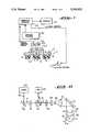
- FIG. 1is a diagrammatic representation of the microscope system of the present invention illustrating a fragment of a photomask as it is inspected by the system.
- FIG. 2is a diagrammatic illustration of the optical arrangement of the microscope of FIG. 1.
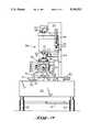
- FIG. 3is a side elevation, partially in section, of the microscope system of the present invention.
- FIG. 4is a diagrammatic illustration of the manner in which light is directed into and reflected by the photomask when utilizing the microscope of the present invention.
- FIG. 5is an isometric view of the substrate thickness compensator mechanism and the mask supporting chuck of the microscope of the present invention.
- the photomask inspection method of the present inventionis particularly adapted to be carried out by and to be useful with a microscope scanning and measuring system such as shown in FIGS. 1-3, and more specifically described and claimed in U.S. Pat. Nos. 4,689,491; 4,748,335 and 4,707,610.
- the disclosures of these prior patentsare herein incorporated by reference into the present application and reference to such patents made be had for a more detailed explanation of the apparatus of the present invention and the operation thereof.
- an optical system 20is there indicated which is controlled by and provides signals to a computer system 22 which outputs information to various display units 24.
- the photomask P to be inspected and measured by the systemunderlies the optical system and is arranged to be moved in a plane lying generally perpendicular to the projected light beam from the optical system 20.
- the mask Pcan be moved over small incremental distances in the x and y orthogonal directions by a mechanical scanning mechanism (not shown in FIG. 1) and in a horizontal plane under the control of signals (x, y scan control) from the computer system 22.
- Movement in the z directioni.e., in a direction generally parallel to the light beam projected from the optical system, is accomplished by a focus control mechanism 28 which shifts an objective lens 26 (part of the optical system) over very small vertical distances in order to change the focal plane of the optical system and thereby bring the focused beam spot to the appropriate plane in the mask P.
- the focus control mechanismis operated from the computer system through a focus control signal to shift the lens 26 up or down as indicated.
- the beam from the optical systemis sharply focused, and it is adapted to be reflected from a surface at or near the focal plane back through the optical system to a photodetector.
- the signal from the photodetectoris digitized by the control circuitry and transmitted to the computer system to represent the intensity of the reflected light from a surface within the photomask P for a plurality of separate, but closely spaced, points in the x-y plane.
- the relevant informationis thereby provided as to the presence or absence of a reflective surface at each of such points. Since the optical system has a very narrow depth of field, reflected intensity peaks at the focal plane and drops off rather sharply as the surface moves away from the focal plane. Thus, only the presence of a reflective surface (metal) at or near the focal plane is detected.
- a conventional photomask Pis comprised of a quartz base or substrate S, a chromium metallic layer M with portions thereof being etched away, and an overlying layer of photoresist Q which remains on the metal during iterative etching processes, as explained previously.
- the photomaskis reversed in position with respect to the optical system from the prior art arrangements; that is to say, the unpatterned side of the substrate S faces the optical system and the patterned face of the mask is directed away from the optical system.
- the scanning beamis therefore directed through the substrate to focus upon the plane which defines the bottom face (top face with the mask reversed as in FIG. 1) of the metallic layer M.
- the photomaskis adapted to be incrementally shifted in the x direction and readings of the intensity of the reflected beam are taken at closely spaced points along a scan line in such direction to determine the presence or absence of the metal surface and thereby define the widths d1 and spacings d of the various metal segments making up metal layer M.
- the maskmay be shifted slightly in the orthogonal y direction to provide a second set of readings along a parallel x-path. In this manner, the dimensions d1 and alignment of the metal lines in the photomask can be accurately determined over the entire area of the mask being scanned.
- a laser source 40provides a closely defined coherent light beam B to a mirror 50 from which the beam is directed through an isolator 51 that allows light to pass only in the direction of the arrow T so as to isolate the laser source from light reflected from the photomask P back through the system.
- a beam splitter 52is provided allowing a portion of the transmitted beam B from the laser source to pass directly therethrough while reflecting a portion of the return beam in the direction of the arrows R so that it will be received by a photomultiplier tube 42.
- An optically birefringent plate 53is provided to control beam polarization in the optical system.
- the present system plate 53is designed as a one- quarter wavelength plate which can be rotated to control the degree of polarization.
- Objective lenses 54 and 55receive both the transmitted beam B and the coincident return beam from the photomask and direct them through a spatial filter 56 which has a small pinhole at the focal point of the two lenses. This pinhole must be smaller than the airy disk of the returning beam; it is typically in the micron, or even submicron, diameter range.
- the objective lens 55recollimates the transmitted beam so that only substantially parallel rays of light emanate therefrom, such beam having a diameter of about 1 centimeter. This beam is reflected by a mirror 57 to change its direction to the vertical, and a controlled aperture device 58 is provided to stop down this beam to the desired size.
- This diameterwill be determined by the amount of area desired to be covered by the focus spot in the photomask with smaller spots obviously being required as the line size of the patterns in the photomask is reduced.
- the objective lens 26, which is movable vertically through the focus control mechanism 28,focusses the transmitted beam B within the mask in a very small spot (typically about 0.3 to about 1 micron in diameter). Scanning is then accomplished, as previously explained, by moving the mask in the x-y plane so that the laser beam successively scans along a series of closely spaced parallel lines over a small portion (the scanning area) of the mask.
- the optical system as illustrated and describedcomprises a confocal imaging system, i.e., a system wherein there are single or multiple point sources and associated single or multiple point detectors coincident at the focal plane within the photomask.
- the pinhole plate 56provides both the point source and the point detector, and the beam of light B and reflected beam both are thus directed through an identical optical system.
- the reflected or returned light beamwill pass back through the objective lenses 26, 55 and 54 and through plate 53.
- the beam splitter 52causes a portion of the beam to be directed at right angles (in the direction of arrows R) to the photomultiplier tube 42.
- the mechanical structure which comprises the photomask scanning apparatus of the present inventionis shown in FIG. 3. It will be seen that the entire photomask drive apparatus and the optical system 20 are arranged to be mounted upon a granite surface plate 60 which is seated upon a table 61 and isolated therefrom by four piston and cylinder type air springs 62 mounted to support each corner of the surface plate (two only being shown in FIG. 3).
- a frame structure 64is elevated above the surface plate 60 to provide support for the optical system module 20 and the focus control mechanism 28.
- the focus control mechanismincludes an electromagnetic drive means for elevating or lowering the objective lens 26 by very small amounts (in the submicron range) so as to change the focal length of the optical system and adjust the projected spot within the photomask P.
- the entire focus control mechanismis mounted within a cage 72 which is adapted to be slid vertically by means of a slidable mount attached to the upright frame 64.
- a support bracket 70is attached to one side of cage 72 projecting outwardly therefrom to support a DC servo motor 66 with the projecting lead screw 67 thereof being adapted to engage the upper face of a support secured to the main upright frame 64.
- movement of the screw 67 within the motor assembly 66serves to raise or lower the objective lens 26 relative to the underlying mask support assembly.
- This lens movementis provided only for gross alignment of the optical system relative to the photomask, i.e., to move the optical system into and out of the basic focal range of the optics.
- Use of the motor 66 to elevate the lens 26 well above the underlying photomaskalso permits the photomask to be readily loaded and unloaded.
- the planar drive arrangement which supports the photomask P in a horizontal plane directly beneath the vertically projected beam from the optical system 20includes a pair of x and y drive devices or stages 34, 32 mounted one above the other and at right angles to each other as shown.
- Each stage 34, 32is comprised of a conventional precision translation table which, in the presently described embodiment of the invention, is designed to have about six to eight inches of linear travel.
- These tableseach include a drive motor 82 which serves to drive a slide block 80 within a channel shaped frame structure 83 by means of a lead screw (not shown) that is threaded to a nut attached to the slide block 80.
- each translation tableincludes an optical position encoder therein with submicron resolution and accuracy which serves to feed continuous position signals back to the computer 22 so that the precise position of the mask P in the x-y plane at any given time can be controlled and correlated with the reflected intensity measurements from the optical system during the operation of the apparatus.
- a flat lower tilt plate 84is firmly attached to the upper face of slide block 80 of the upper, or y-stage, translation table 32, and a middle tilt plate 86 is secured thereto by means of leaf spring 88 which is rigidly bolted to the adjacent spaced ends of both of the tilt plates.
- Tilt adjusting screw 87is threaded through the end of tilt plate 86 opposite to the mounting of spring 88 so as to bear against the upper surface of lower tilt plate 84 so that the middle tilt plate (and the structure supported thereabove) can be tilted about the X-axis by adjustment of the screw 87.
- an upper tilt plate 90is secured in spaced relationship to the middle tilt plate 86 by means of a leaf spring 92 bolted to the rearward edges of the tilt plate, and a tilt adjusting screw 91 is threaded through the forward edge of tilt plate 90 to bear against the upper surface of tilt plate 86 so as to adjustably rotate the tilt plate 90 about the Y-axis.
- the vibratory scanner mechanism 46by which the photomask P is rapidly vibrated in the direction of the x-axis, includes an electromagnetic driver 100 secured to the upper face of tilt block 90 and having an armature secured to a spring-mounted and elevated vibratory driving mechanism 102 positioned above the tilt block 90 and adapted to be vibrated in the x direction and parallel to tilt block 90 (i.e., horizontally), as shown by the arrow in FIG. 3.
- a vacuum chuck 89is supported by the movable portion of the vibratory driving mechanism 102 to support and maintain the photomask in a fixed position beneath the scanning beam from the optical system.
- a substrate thickness compensator mechanism 110which is mounted for pivotal movement about the drive axis of a stepper motor 112 as shown and which serves to selectively place a glass plate between the photomask P and the overlying optical system to compensate for a particular thickness of substrate of the photomask undergoing inspection which may be different from the substrate thickness for which the optical system is set in a manner to be described in greater detail hereinafter.
- the stepper motoris mounted upon a bracket 114 attached to the main upright frame 64 of the apparatus.
- FIG. 4illustrates the manner in which the system of the present invention operates to scan a photomask undergoing an iterative etching process.
- the beam B from the objective lens 26 of the optical systemis arranged to be focused on the plane defining the substrate-metal (S-M) interface.
- an objective lensis used which is specially corrected for diffraction limited operation through the thickness of photomask substrate being examined.
- Lenses of this typeare conventionally used for examining biospecimens inside plastic incubation vessels. As can be seen, the rays of light from the lens are focused at one angle while moving through air and at a different, less sharp, angle when moving through the quartz substrate due to the differing refractive indices.
- the corrected lens 26is chosen to accommodate a maximum thickness of substrate S.
- a compensator disc, or optical plate, 120is arranged to be placed between the mask and the lens 26 so that the combined optical thickness of substrate and compensator disc generally equals the actual glass thickness for which the corrected lens 26 is set.
- a 488 nm wavelength lasercan be used as the light source, and a 0.55 N.A. lens corrected for a maximum thickness of substrate of 0.25 inches can be used as objective lens 26.
- An Olympus ULWD CD Plan 40 lenswas found to be adequate but it had to be modified for measuring through the relatively thick glass found in conventional photomask substrates.
- the width d1 of a metal line or segment Mcan be accurately determined. This is particularly important when the inspection occurs during an iterative etching process. As shown in FIG. 4, the initial application of acid to the photomask may result in relatively wide edges 130a defining the metal segments. Measurements of segment widths d1a are then made using the apparatus as aforedescribed. Since this is greater than the desired segment widths d1 (as defined by edges 130) the process is continued for a period of time felt to be sufficient to complete the etching process with such time being calculated from the measured widths d1 as first determined.
- a second, intermediate etching stepmay be monitored when the metal segments have widths d1b (defined by edges 130b), with the remaining etching time being again calculated based on the measured widths d1b.
- the desired segment widths d1are achieved and can be readily checked while the photoresist Q remains in place on the undercut metal segments. Since the measurement determinations are unaffected by the photoresist Q and undistorted thereby, it will be appreciated that a significant increase in the accuracy of the measurements is obtained with the method and system of the present invention.
- the substrate compensator mechanism 110is shown in detail in FIG. 5.
- the stepper motor 112is appropriately controlled to rotate its drive shaft and a disc carrier 116 pinned thereto through a selectable series of angular positions.
- the carrier 116is fork-shaped with a pair of legs 116a and 116b projecting at right angles to the upper body of the carrier so that they can be individually positioned parallel to and closely overlying that area of the photomask P to be scanned.
- Each leg 116a, 116bhas a recessed aperture into which is securely fitted the glass disc 120a, 120b that serves as the aforedescribed compensating glass plate to accommodate the particular mask substrate being inspected.
- the carriermay be rotated through three different positions by the stepper motor: (1) both legs 116a, 116b pivoted away from the mask and out of the beam path; (2) leg 116a overlying the mask with disc 120a receiving the projected beam of the optical system (as shown in FIG. 5); and (3) leg 116b overlying the mask with disk 120b receiving the projected beam.
- the discs 120a, 120bare obviously of different thicknesses to accommodate different substrate thicknesses.
- compensator discsof 0.1 inch and 0.16 inches have been chosen thereby providing for mask substrate thicknesses of 0.15 inches and 0.09 inches, respectively.
- additional legs and supported discs 120may be added to the carrier 116 if desired in order to increase the available options.
- FIG. 5also indicates the desired configuration of the chuck 89 for supporting the photomask P during the inspection process.
- the upper face of the chuckis provided with a recess 132 into which the mask is adapted to be placed and wherein it is arranged to be supported only along its peripheral edges by a narrow support ledge 134.
- Located at spaced positions about the support ledgeare a plurality of vacuum slots 136 (one only shown in FIG. 5) which, when a vacuum source is applied thereto, serve to solidly fix the mask upon the chuck and prevent any relative movement thereof during the scanning operation.
- the large central recess 138 of the chuckunderlies the entire patterned face of the photomask so as to prevent any contact with and possible damage by the hard surface of the chuck.
- the present inventioncould have been incorporated in many other types of scanning or imaging optical microscopes designed for metrology applications operating at diverse visible or invisible wavelengths, such as: video microscopes including a video camera and optical microscope, Nipkow disc confocal microscopes, slit-scanning microscopes, beam scanning optical microscopes, object scanning microscopes and image shearing microscopes.
- video microscopesincluding a video camera and optical microscope
- Nipkow disc confocal microscopesslit-scanning microscopes
- beam scanning optical microscopesobject scanning microscopes
- image shearing microscopesimage shearing microscopes.
- the present inventionmay be utilized with a non-scanning type of microscope wherein the entire area of the substrate of the photomask to be viewed is flooded with light and a video camera views such area and senses the reflected light intensity over a plurality of closely spaced points in a grid at the metal-substrate interface.
- a compensating platemay be inserted between the objective lens of such a video cameramicroscope system and the
- the method and apparatus of the present inventionhas utility in inspecting photomasks such as might be used in phase-shift lithography techniques wherein the mask varies in thickness and may be made of diverse patterned materials.
- the optical system as describedmay be focussed on a plane of interest which, for example, may be defined by the lowermost surfaces of the recesses on the patterned face of the mask. It will be appreciated that this plane of interest may be inspected with no distortion of the projected and reflected beams as would occur when imaging from the patterned side of the mask. Even multi-layered photomasks may be conveniently inspected with the system of the present invention by viewing into such masks through their unpatterned faces.
Landscapes
- Physics & Mathematics (AREA)
- General Physics & Mathematics (AREA)
- Length Measuring Devices By Optical Means (AREA)
- Measurement Of Optical Distance (AREA)
- Instruments For Measurement Of Length By Optical Means (AREA)
Abstract
Description
Claims (18)
Priority Applications (2)
| Application Number | Priority Date | Filing Date | Title |
|---|---|---|---|
| US07/719,519US5184021A (en) | 1991-06-24 | 1991-06-24 | Method and apparatus for measuring the dimensions of patterned features on a lithographic photomask |
| JP4179144AJP3042187B2 (en) | 1991-06-24 | 1992-06-12 | Method and apparatus for measuring the dimensions of a patterned structure of a lithographic photomask |
Applications Claiming Priority (1)
| Application Number | Priority Date | Filing Date | Title |
|---|---|---|---|
| US07/719,519US5184021A (en) | 1991-06-24 | 1991-06-24 | Method and apparatus for measuring the dimensions of patterned features on a lithographic photomask |
Publications (1)
| Publication Number | Publication Date |
|---|---|
| US5184021Atrue US5184021A (en) | 1993-02-02 |
Family
ID=24890386
Family Applications (1)
| Application Number | Title | Priority Date | Filing Date |
|---|---|---|---|
| US07/719,519Expired - LifetimeUS5184021A (en) | 1991-06-24 | 1991-06-24 | Method and apparatus for measuring the dimensions of patterned features on a lithographic photomask |
Country Status (2)
| Country | Link |
|---|---|
| US (1) | US5184021A (en) |
| JP (1) | JP3042187B2 (en) |
Cited By (23)
| Publication number | Priority date | Publication date | Assignee | Title |
|---|---|---|---|---|
| US5607800A (en)* | 1995-02-15 | 1997-03-04 | Lucent Technologies Inc. | Method and arrangement for characterizing micro-size patterns |
| US5719700A (en)* | 1991-10-11 | 1998-02-17 | L'oreal | Apparatus for in vivo observation of the microscopic structure of the skin or of a similar tissue |
| WO1998049538A1 (en)* | 1994-12-20 | 1998-11-05 | International Business Machines Corporation | Monitoring of minimum features on a substrate |
| US6323953B1 (en) | 1998-04-30 | 2001-11-27 | Leica Microsystems Wetzlar Gmbh | Method and device for measuring structures on a transparent substrate |
| US6327035B1 (en) | 1999-11-30 | 2001-12-04 | Nsh Technology, Inc. | Method and apparatus for optically examining miniature patterns |
| US6548796B1 (en) | 1999-06-23 | 2003-04-15 | Regents Of The University Of Minnesota | Confocal macroscope |
| US20040115539A1 (en)* | 2002-09-11 | 2004-06-17 | Broeke Doug Van Den | Method of achieving CD linearity control for full-chip CPL manufacturing |
| US20040263850A1 (en)* | 2003-06-25 | 2004-12-30 | Guoguang Li | Method and apparatus for examining features on semi-transparent and transparent substrates |
| US6867406B1 (en) | 1999-03-23 | 2005-03-15 | Kla-Tencor Corporation | Confocal wafer inspection method and apparatus using fly lens arrangement |
| US20060087660A1 (en)* | 2002-05-15 | 2006-04-27 | John Zabolitzky | Device for measuring in three dimensions a topographical shape of an object |
| US20060116851A1 (en)* | 2004-11-26 | 2006-06-01 | Olympus Corporation | Apparatus and method for three-dimensional measurement and program for allowing computer to execute method for three-dimensional measurement |
| CN100437220C (en)* | 2004-01-22 | 2008-11-26 | Ntn株式会社 | Micro-pattern observer and micro-pattern revision device therewith |
| US8586947B1 (en)* | 2008-05-05 | 2013-11-19 | Illumina, Inc. | Compensator for multiple surface imaging |
| WO2012012265A3 (en)* | 2010-07-23 | 2014-03-27 | Zeta Instruments, Inc. | 3d microscope and methods of measuring patterned substrates |
| WO2015078633A1 (en)* | 2013-11-27 | 2015-06-04 | Carl Zeiss Microscopy Gmbh | Light microscope having internal focus lens and microscopy method for examining a plurality of microscopic objects |
| US20180045937A1 (en)* | 2016-08-10 | 2018-02-15 | Zeta Instruments, Inc. | Automated 3-d measurement |
| US10486153B2 (en) | 2013-09-27 | 2019-11-26 | Illumina, Inc. | Method to produce chemical pattern in micro-fluidic structure |
| US10704094B1 (en) | 2018-11-14 | 2020-07-07 | Element Biosciences, Inc. | Multipart reagents having increased avidity for polymerase binding |
| US10768173B1 (en) | 2019-09-06 | 2020-09-08 | Element Biosciences, Inc. | Multivalent binding composition for nucleic acid analysis |
| US10876148B2 (en) | 2018-11-14 | 2020-12-29 | Element Biosciences, Inc. | De novo surface preparation and uses thereof |
| US11287422B2 (en) | 2019-09-23 | 2022-03-29 | Element Biosciences, Inc. | Multivalent binding composition for nucleic acid analysis |
| US11426732B2 (en) | 2018-12-07 | 2022-08-30 | Element Biosciences, Inc. | Flow cell device and use thereof |
| US12083514B2 (en) | 2018-07-03 | 2024-09-10 | Illumina, Inc. | Interposer with first and second adhesive layers |
Families Citing this family (1)
| Publication number | Priority date | Publication date | Assignee | Title |
|---|---|---|---|---|
| KR101776190B1 (en)* | 2014-09-19 | 2017-09-08 | 삼성디스플레이 주식회사 | Apparatus and method for stick |
Citations (9)
| Publication number | Priority date | Publication date | Assignee | Title |
|---|---|---|---|---|
| US3560093A (en)* | 1968-07-16 | 1971-02-02 | Western Electric Co | Superimposed common carrier mask inspection system |
| US4541715A (en)* | 1982-01-12 | 1985-09-17 | Hitachi, Ltd. | Apparatus for detecting contaminants on the reticle of exposure system |
| US4707610A (en)* | 1985-07-03 | 1987-11-17 | Siscan Systems, Inc. | Method and apparatus for measuring surface profiles |
| US4718767A (en)* | 1983-10-03 | 1988-01-12 | Nippon Kogaku K.K. | Method of inspecting the pattern on a photographic mask |
| US4748335A (en)* | 1985-04-19 | 1988-05-31 | Siscan Systems, Inc. | Method and aparatus for determining surface profiles |
| US4806774A (en)* | 1987-06-08 | 1989-02-21 | Insystems, Inc. | Inspection system for array of microcircuit dies having redundant circuit patterns |
| US4814626A (en)* | 1985-12-13 | 1989-03-21 | Siemens Aktiengesellschaft | Method for high precision position measurement of two-dimensional structures |
| US5004321A (en)* | 1989-07-28 | 1991-04-02 | At&T Bell Laboratories | Resolution confocal microscope, and device fabrication method using same |
| US5078482A (en)* | 1989-07-28 | 1992-01-07 | At&T Bell Laboratories | Resolution confocal microscope, and device fabrication method using same |
- 1991
- 1991-06-24USUS07/719,519patent/US5184021A/ennot_activeExpired - Lifetime
- 1992
- 1992-06-12JPJP4179144Apatent/JP3042187B2/ennot_activeExpired - Fee Related
Patent Citations (9)
| Publication number | Priority date | Publication date | Assignee | Title |
|---|---|---|---|---|
| US3560093A (en)* | 1968-07-16 | 1971-02-02 | Western Electric Co | Superimposed common carrier mask inspection system |
| US4541715A (en)* | 1982-01-12 | 1985-09-17 | Hitachi, Ltd. | Apparatus for detecting contaminants on the reticle of exposure system |
| US4718767A (en)* | 1983-10-03 | 1988-01-12 | Nippon Kogaku K.K. | Method of inspecting the pattern on a photographic mask |
| US4748335A (en)* | 1985-04-19 | 1988-05-31 | Siscan Systems, Inc. | Method and aparatus for determining surface profiles |
| US4707610A (en)* | 1985-07-03 | 1987-11-17 | Siscan Systems, Inc. | Method and apparatus for measuring surface profiles |
| US4814626A (en)* | 1985-12-13 | 1989-03-21 | Siemens Aktiengesellschaft | Method for high precision position measurement of two-dimensional structures |
| US4806774A (en)* | 1987-06-08 | 1989-02-21 | Insystems, Inc. | Inspection system for array of microcircuit dies having redundant circuit patterns |
| US5004321A (en)* | 1989-07-28 | 1991-04-02 | At&T Bell Laboratories | Resolution confocal microscope, and device fabrication method using same |
| US5078482A (en)* | 1989-07-28 | 1992-01-07 | At&T Bell Laboratories | Resolution confocal microscope, and device fabrication method using same |
Cited By (51)
| Publication number | Priority date | Publication date | Assignee | Title |
|---|---|---|---|---|
| US5719700A (en)* | 1991-10-11 | 1998-02-17 | L'oreal | Apparatus for in vivo observation of the microscopic structure of the skin or of a similar tissue |
| WO1998049538A1 (en)* | 1994-12-20 | 1998-11-05 | International Business Machines Corporation | Monitoring of minimum features on a substrate |
| US5607800A (en)* | 1995-02-15 | 1997-03-04 | Lucent Technologies Inc. | Method and arrangement for characterizing micro-size patterns |
| US6323953B1 (en) | 1998-04-30 | 2001-11-27 | Leica Microsystems Wetzlar Gmbh | Method and device for measuring structures on a transparent substrate |
| US6867406B1 (en) | 1999-03-23 | 2005-03-15 | Kla-Tencor Corporation | Confocal wafer inspection method and apparatus using fly lens arrangement |
| US7858911B2 (en) | 1999-03-23 | 2010-12-28 | Kla-Tencor Corporation | Confocal wafer inspection system and method |
| US20070007429A1 (en)* | 1999-03-23 | 2007-01-11 | Kla-Tencor Corporation | Confocal wafer inspection method and apparatus using fly lens arrangement |
| US7399950B2 (en) | 1999-03-23 | 2008-07-15 | Kla-Tencor Corporation | Confocal wafer inspection method and apparatus using fly lens arrangement |
| US20080273196A1 (en)* | 1999-03-23 | 2008-11-06 | Kla-Tencor Corporation | Confocal wafer inspection system and method |
| US20050156098A1 (en)* | 1999-03-23 | 2005-07-21 | Fairley Christopher R. | Confocal wafer inspection method and apparatus |
| US7109458B2 (en) | 1999-03-23 | 2006-09-19 | Kla-Tencor Corporation | Confocal wafer depth scanning inspection method |
| US6548796B1 (en) | 1999-06-23 | 2003-04-15 | Regents Of The University Of Minnesota | Confocal macroscope |
| US20030151742A1 (en)* | 1999-06-23 | 2003-08-14 | Regents Of The University Of Minnesota | Confocal macroscope |
| US6327035B1 (en) | 1999-11-30 | 2001-12-04 | Nsh Technology, Inc. | Method and apparatus for optically examining miniature patterns |
| US20060087660A1 (en)* | 2002-05-15 | 2006-04-27 | John Zabolitzky | Device for measuring in three dimensions a topographical shape of an object |
| US7446885B2 (en)* | 2002-05-15 | 2008-11-04 | Icos Vision Systems N.V. | Device for measuring in three dimensions a topographical shape of an object |
| US7667216B2 (en) | 2002-09-11 | 2010-02-23 | Asml Masktools B.V. | Method of achieving CD linearity control for full-chip CPL manufacturing |
| US7211815B2 (en) | 2002-09-11 | 2007-05-01 | Asml Masktools B.V. | Method of achieving CD linearity control for full-chip CPL manufacturing |
| SG118203A1 (en)* | 2002-09-11 | 2006-01-27 | Asml Masktools Bv | Method of achieving CD linearity control for a full-chip cpl manufacturing |
| US20040115539A1 (en)* | 2002-09-11 | 2004-06-17 | Broeke Doug Van Den | Method of achieving CD linearity control for full-chip CPL manufacturing |
| US7253909B1 (en) | 2003-06-25 | 2007-08-07 | N&K Technology, Inc. | Phase shift measurement using transmittance spectra |
| US6891628B2 (en) | 2003-06-25 | 2005-05-10 | N & K Technology, Inc. | Method and apparatus for examining features on semi-transparent and transparent substrates |
| US20040263850A1 (en)* | 2003-06-25 | 2004-12-30 | Guoguang Li | Method and apparatus for examining features on semi-transparent and transparent substrates |
| CN100437220C (en)* | 2004-01-22 | 2008-11-26 | Ntn株式会社 | Micro-pattern observer and micro-pattern revision device therewith |
| US20060116851A1 (en)* | 2004-11-26 | 2006-06-01 | Olympus Corporation | Apparatus and method for three-dimensional measurement and program for allowing computer to execute method for three-dimensional measurement |
| US7436524B2 (en)* | 2004-11-26 | 2008-10-14 | Olympus Corporation | Apparatus and method for three-dimensional measurement and program for allowing computer to execute method for three-dimensional measurement |
| USRE48561E1 (en) | 2008-05-05 | 2021-05-18 | Illumina, Inc. | Compensator for multiple surface imaging |
| USRE48219E1 (en) | 2008-05-05 | 2020-09-22 | Illumina, Inc. | Compensator for multiple surface imaging |
| USRE49884E1 (en) | 2008-05-05 | 2024-03-26 | Illumina, Inc. | Compensator for multiple surface imaging |
| US8586947B1 (en)* | 2008-05-05 | 2013-11-19 | Illumina, Inc. | Compensator for multiple surface imaging |
| US9389408B2 (en) | 2010-07-23 | 2016-07-12 | Zeta Instruments, Inc. | 3D microscope and methods of measuring patterned substrates |
| CN107229116A (en)* | 2010-07-23 | 2017-10-03 | 泽伊塔仪器科技(上海)有限公司 | The 3D microscopes and method of measurement pattern substrate |
| US10209501B2 (en) | 2010-07-23 | 2019-02-19 | Kla-Tencor Corporation | 3D microscope and methods of measuring patterned substrates |
| WO2012012265A3 (en)* | 2010-07-23 | 2014-03-27 | Zeta Instruments, Inc. | 3d microscope and methods of measuring patterned substrates |
| US12303888B2 (en) | 2013-09-27 | 2025-05-20 | Illumina, Inc. | Method to produce chemical pattern in micro-fluidic structure |
| US10486153B2 (en) | 2013-09-27 | 2019-11-26 | Illumina, Inc. | Method to produce chemical pattern in micro-fluidic structure |
| US11298697B2 (en) | 2013-09-27 | 2022-04-12 | Illumina, Inc. | Method to produce chemical pattern in micro-fluidic structure |
| US10422983B2 (en) | 2013-11-27 | 2019-09-24 | Max-Planck-Gesellschaft Zur Foerderung Der Wissenschaften E. V. | Light microscope with inner focusing objective and microscopy method for examining a plurality of microscopic objects |
| US10634888B2 (en) | 2013-11-27 | 2020-04-28 | Max-Planck-Gesellschaft Zur Foerderung Der Wissenschaften E. V. | Light microscope with inner focusing objective and microscopy method for examining a plurality of microscopic objects |
| WO2015078633A1 (en)* | 2013-11-27 | 2015-06-04 | Carl Zeiss Microscopy Gmbh | Light microscope having internal focus lens and microscopy method for examining a plurality of microscopic objects |
| US20180045937A1 (en)* | 2016-08-10 | 2018-02-15 | Zeta Instruments, Inc. | Automated 3-d measurement |
| US12083514B2 (en) | 2018-07-03 | 2024-09-10 | Illumina, Inc. | Interposer with first and second adhesive layers |
| US10876148B2 (en) | 2018-11-14 | 2020-12-29 | Element Biosciences, Inc. | De novo surface preparation and uses thereof |
| US10982280B2 (en) | 2018-11-14 | 2021-04-20 | Element Biosciences, Inc. | Multipart reagents having increased avidity for polymerase binding |
| US10704094B1 (en) | 2018-11-14 | 2020-07-07 | Element Biosciences, Inc. | Multipart reagents having increased avidity for polymerase binding |
| US12331356B2 (en) | 2018-11-14 | 2025-06-17 | Element Biosciences, Inc. | Multipart reagents having increased avidity for polymerase binding |
| US11426732B2 (en) | 2018-12-07 | 2022-08-30 | Element Biosciences, Inc. | Flow cell device and use thereof |
| US12117438B2 (en) | 2019-09-06 | 2024-10-15 | Element Biosciences, Inc. | Multivalent binding composition for nucleic acid analysis |
| US10768173B1 (en) | 2019-09-06 | 2020-09-08 | Element Biosciences, Inc. | Multivalent binding composition for nucleic acid analysis |
| US12241891B2 (en) | 2019-09-23 | 2025-03-04 | Element Biosciences, Inc. | Multivalent binding composition for nucleic acid analysis |
| US11287422B2 (en) | 2019-09-23 | 2022-03-29 | Element Biosciences, Inc. | Multivalent binding composition for nucleic acid analysis |
Also Published As
| Publication number | Publication date |
|---|---|
| JP3042187B2 (en) | 2000-05-15 |
| JPH05187828A (en) | 1993-07-27 |
Similar Documents
| Publication | Publication Date | Title |
|---|---|---|
| US5184021A (en) | Method and apparatus for measuring the dimensions of patterned features on a lithographic photomask | |
| KR100567968B1 (en) | Focusing and tilting adjustment system for lithography aligner, manufacturing apparatus of inspection apparatus | |
| US6376329B1 (en) | Semiconductor wafer alignment using backside illumination | |
| US7738113B1 (en) | Wafer measurement system and apparatus | |
| US6624879B2 (en) | Exposure apparatus and method for photolithography | |
| KR100592570B1 (en) | Lithography Projection Equipment | |
| US4748335A (en) | Method and aparatus for determining surface profiles | |
| US5999245A (en) | Proximity exposure device with distance adjustment device | |
| JP4163258B2 (en) | Optical height measuring device, surface inspection device having such a height measuring device, and lithographic device having this inspection device | |
| US5638206A (en) | Confocal optical microscope and length measuring device using this microscope | |
| KR20090113895A (en) | Defect measuring device of glass sheet | |
| TW569304B (en) | Focusing method, position measuring method, exposure method, device manufacturing method and exposure apparatus | |
| US4932781A (en) | Gap measuring apparatus using interference fringes of reflected light | |
| US20200355724A1 (en) | System and method for optical drift correction | |
| TWI765361B (en) | Method for determining surface parameters of a patterning device, method for compensating a heating effect and lithographic apparatus for characterizing a patterning device | |
| JPS63131116A (en) | confocal microscope | |
| WO2003060589A1 (en) | Auto focussing device and method | |
| US7177019B2 (en) | Apparatus for imaging metrology | |
| JP4646342B2 (en) | Thin film magnetic head size / array measuring method and thin film magnetic head size / array measuring apparatus | |
| JP2000012452A (en) | Exposure equipment | |
| JPH0682381A (en) | Foreign matter inspection device | |
| WO2020009762A1 (en) | A system and method for making accurate grating patterns using multiple writing columns each making multiple scans | |
| JP3101582B2 (en) | Position detecting apparatus and method using oblique optical axis optical system | |
| JPH0861939A (en) | Method and apparatus for measuring surface state of substrate holder | |
| JPH0683037A (en) | Reticle mask shape defect inspection system |
Legal Events
| Date | Code | Title | Description |
|---|---|---|---|
| AS | Assignment | Owner name:SISCAN SYSTEMS, INC. A CA CORPORATION, CALIFORN Free format text:ASSIGNMENT OF ASSIGNORS INTEREST.;ASSIGNOR:SMITH, IAN R.;REEL/FRAME:006088/0143 Effective date:19920409 | |
| STCF | Information on status: patent grant | Free format text:PATENTED CASE | |
| AS | Assignment | Owner name:OPTICAL ASSOCIATES, INC., CALIFORNIA Free format text:ASSIGNMENT OF ASSIGNORS INTEREST;ASSIGNOR:SISCAN SYSTEMS, INC.;REEL/FRAME:006867/0431 Effective date:19940118 | |
| AS | Assignment | Owner name:SILICON VALLEY BANK, CALIFORNIA Free format text:SECURITY INTEREST;ASSIGNOR:OPTICAL ASSOCIATES, INC.;REEL/FRAME:007179/0944 Effective date:19931021 | |
| FPAY | Fee payment | Year of fee payment:4 | |
| AS | Assignment | Owner name:ISHIKAWAJIMA-HARIMA HEAVY INDUSTRIES CO., LTD., JA Free format text:ASSIGNMENT OF ASSIGNORS INTEREST;ASSIGNOR:OPTICAL ASSOCIATES, INC.;REEL/FRAME:008753/0604 Effective date:19970124 | |
| FEPP | Fee payment procedure | Free format text:PAT HLDR NO LONGER CLAIMS SMALL ENT STAT AS INDIV INVENTOR (ORIGINAL EVENT CODE: LSM1); ENTITY STATUS OF PATENT OWNER: LARGE ENTITY | |
| FPAY | Fee payment | Year of fee payment:8 | |
| FEPP | Fee payment procedure | Free format text:PAYER NUMBER DE-ASSIGNED (ORIGINAL EVENT CODE: RMPN); ENTITY STATUS OF PATENT OWNER: LARGE ENTITY Free format text:PAYOR NUMBER ASSIGNED (ORIGINAL EVENT CODE: ASPN); ENTITY STATUS OF PATENT OWNER: LARGE ENTITY | |
| FPAY | Fee payment | Year of fee payment:12 |