US5181859A - Electrical connector circuit wafer - Google Patents
Electrical connector circuit waferDownload PDFInfo
- Publication number
- US5181859A US5181859AUS07/895,148US89514892AUS5181859AUS 5181859 AUS5181859 AUS 5181859AUS 89514892 AUS89514892 AUS 89514892AUS 5181859 AUS5181859 AUS 5181859A
- Authority
- US
- United States
- Prior art keywords
- wafer
- pins
- male connector
- male
- connector
- Prior art date
- Legal status (The legal status is an assumption and is not a legal conclusion. Google has not performed a legal analysis and makes no representation as to the accuracy of the status listed.)
- Expired - Lifetime
Links
Images


Classifications
- H—ELECTRICITY
- H01—ELECTRIC ELEMENTS
- H01R—ELECTRICALLY-CONDUCTIVE CONNECTIONS; STRUCTURAL ASSOCIATIONS OF A PLURALITY OF MUTUALLY-INSULATED ELECTRICAL CONNECTING ELEMENTS; COUPLING DEVICES; CURRENT COLLECTORS
- H01R13/00—Details of coupling devices of the kinds covered by groups H01R12/70 or H01R24/00 - H01R33/00
- H01R13/66—Structural association with built-in electrical component
- H01R13/6608—Structural association with built-in electrical component with built-in single component
- H01R13/6616—Structural association with built-in electrical component with built-in single component with resistor
- H—ELECTRICITY
- H01—ELECTRIC ELEMENTS
- H01R—ELECTRICALLY-CONDUCTIVE CONNECTIONS; STRUCTURAL ASSOCIATIONS OF A PLURALITY OF MUTUALLY-INSULATED ELECTRICAL CONNECTING ELEMENTS; COUPLING DEVICES; CURRENT COLLECTORS
- H01R12/00—Structural associations of a plurality of mutually-insulated electrical connecting elements, specially adapted for printed circuits, e.g. printed circuit boards [PCB], flat or ribbon cables, or like generally planar structures, e.g. terminal strips, terminal blocks; Coupling devices specially adapted for printed circuits, flat or ribbon cables, or like generally planar structures; Terminals specially adapted for contact with, or insertion into, printed circuits, flat or ribbon cables, or like generally planar structures
- H01R12/70—Coupling devices
- G—PHYSICS
- G06—COMPUTING OR CALCULATING; COUNTING
- G06F—ELECTRIC DIGITAL DATA PROCESSING
- G06F21/00—Security arrangements for protecting computers, components thereof, programs or data against unauthorised activity
- H—ELECTRICITY
- H01—ELECTRIC ELEMENTS
- H01R—ELECTRICALLY-CONDUCTIVE CONNECTIONS; STRUCTURAL ASSOCIATIONS OF A PLURALITY OF MUTUALLY-INSULATED ELECTRICAL CONNECTING ELEMENTS; COUPLING DEVICES; CURRENT COLLECTORS
- H01R13/00—Details of coupling devices of the kinds covered by groups H01R12/70 or H01R24/00 - H01R33/00
- H01R13/62—Means for facilitating engagement or disengagement of coupling parts or for holding them in engagement
- H01R13/639—Additional means for holding or locking coupling parts together, after engagement, e.g. separate keylock, retainer strap
- H01R13/6397—Additional means for holding or locking coupling parts together, after engagement, e.g. separate keylock, retainer strap with means for preventing unauthorised use
- H—ELECTRICITY
- H01—ELECTRIC ELEMENTS
- H01R—ELECTRICALLY-CONDUCTIVE CONNECTIONS; STRUCTURAL ASSOCIATIONS OF A PLURALITY OF MUTUALLY-INSULATED ELECTRICAL CONNECTING ELEMENTS; COUPLING DEVICES; CURRENT COLLECTORS
- H01R13/00—Details of coupling devices of the kinds covered by groups H01R12/70 or H01R24/00 - H01R33/00
- H01R13/66—Structural association with built-in electrical component
- H01R13/665—Structural association with built-in electrical component with built-in electronic circuit
- H01R13/6658—Structural association with built-in electrical component with built-in electronic circuit on printed circuit board
- H—ELECTRICITY
- H01—ELECTRIC ELEMENTS
- H01R—ELECTRICALLY-CONDUCTIVE CONNECTIONS; STRUCTURAL ASSOCIATIONS OF A PLURALITY OF MUTUALLY-INSULATED ELECTRICAL CONNECTING ELEMENTS; COUPLING DEVICES; CURRENT COLLECTORS
- H01R13/00—Details of coupling devices of the kinds covered by groups H01R12/70 or H01R24/00 - H01R33/00
- H01R13/66—Structural association with built-in electrical component
- H01R13/665—Structural association with built-in electrical component with built-in electronic circuit
- H01R13/6666—Structural association with built-in electrical component with built-in electronic circuit with built-in overvoltage protection
- H—ELECTRICITY
- H01—ELECTRIC ELEMENTS
- H01R—ELECTRICALLY-CONDUCTIVE CONNECTIONS; STRUCTURAL ASSOCIATIONS OF A PLURALITY OF MUTUALLY-INSULATED ELECTRICAL CONNECTING ELEMENTS; COUPLING DEVICES; CURRENT COLLECTORS
- H01R29/00—Coupling parts for selective co-operation with a counterpart in different ways to establish different circuits, e.g. for voltage selection, for series-parallel selection, programmable connectors
- H—ELECTRICITY
- H02—GENERATION; CONVERSION OR DISTRIBUTION OF ELECTRIC POWER
- H02J—CIRCUIT ARRANGEMENTS OR SYSTEMS FOR SUPPLYING OR DISTRIBUTING ELECTRIC POWER; SYSTEMS FOR STORING ELECTRIC ENERGY
- H02J7/00—Circuit arrangements for charging or depolarising batteries or for supplying loads from batteries
- H02J7/00032—Circuit arrangements for charging or depolarising batteries or for supplying loads from batteries characterised by data exchange
- H02J7/00036—Charger exchanging data with battery
- H—ELECTRICITY
- H02—GENERATION; CONVERSION OR DISTRIBUTION OF ELECTRIC POWER
- H02J—CIRCUIT ARRANGEMENTS OR SYSTEMS FOR SUPPLYING OR DISTRIBUTING ELECTRIC POWER; SYSTEMS FOR STORING ELECTRIC ENERGY
- H02J7/00—Circuit arrangements for charging or depolarising batteries or for supplying loads from batteries
- H02J7/00047—Circuit arrangements for charging or depolarising batteries or for supplying loads from batteries with provisions for charging different types of batteries
- H—ELECTRICITY
- H05—ELECTRIC TECHNIQUES NOT OTHERWISE PROVIDED FOR
- H05K—PRINTED CIRCUITS; CASINGS OR CONSTRUCTIONAL DETAILS OF ELECTRIC APPARATUS; MANUFACTURE OF ASSEMBLAGES OF ELECTRICAL COMPONENTS
- H05K1/00—Printed circuits
- H05K1/02—Details
- H05K1/0213—Electrical arrangements not otherwise provided for
- H05K1/0216—Reduction of cross-talk, noise or electromagnetic interference
- H05K1/023—Reduction of cross-talk, noise or electromagnetic interference using auxiliary mounted passive components or auxiliary substances
- H05K1/0231—Capacitors or dielectric substances
- H—ELECTRICITY
- H01—ELECTRIC ELEMENTS
- H01R—ELECTRICALLY-CONDUCTIVE CONNECTIONS; STRUCTURAL ASSOCIATIONS OF A PLURALITY OF MUTUALLY-INSULATED ELECTRICAL CONNECTING ELEMENTS; COUPLING DEVICES; CURRENT COLLECTORS
- H01R13/00—Details of coupling devices of the kinds covered by groups H01R12/70 or H01R24/00 - H01R33/00
- H01R13/66—Structural association with built-in electrical component
- H01R13/6608—Structural association with built-in electrical component with built-in single component
- H01R13/6625—Structural association with built-in electrical component with built-in single component with capacitive component
- H—ELECTRICITY
- H01—ELECTRIC ELEMENTS
- H01R—ELECTRICALLY-CONDUCTIVE CONNECTIONS; STRUCTURAL ASSOCIATIONS OF A PLURALITY OF MUTUALLY-INSULATED ELECTRICAL CONNECTING ELEMENTS; COUPLING DEVICES; CURRENT COLLECTORS
- H01R31/00—Coupling parts supported only by co-operation with counterpart
- H01R31/06—Intermediate parts for linking two coupling parts, e.g. adapter
- H01R31/065—Intermediate parts for linking two coupling parts, e.g. adapter with built-in electric apparatus
- H—ELECTRICITY
- H01—ELECTRIC ELEMENTS
- H01R—ELECTRICALLY-CONDUCTIVE CONNECTIONS; STRUCTURAL ASSOCIATIONS OF A PLURALITY OF MUTUALLY-INSULATED ELECTRICAL CONNECTING ELEMENTS; COUPLING DEVICES; CURRENT COLLECTORS
- H01R9/00—Structural associations of a plurality of mutually-insulated electrical connecting elements, e.g. terminal strips or terminal blocks; Terminals or binding posts mounted upon a base or in a case; Bases therefor
- H01R9/03—Connectors arranged to contact a plurality of the conductors of a multiconductor cable, e.g. tapping connections
- H—ELECTRICITY
- H05—ELECTRIC TECHNIQUES NOT OTHERWISE PROVIDED FOR
- H05K—PRINTED CIRCUITS; CASINGS OR CONSTRUCTIONAL DETAILS OF ELECTRIC APPARATUS; MANUFACTURE OF ASSEMBLAGES OF ELECTRICAL COMPONENTS
- H05K1/00—Printed circuits
- H05K1/18—Printed circuits structurally associated with non-printed electric components
- H—ELECTRICITY
- H05—ELECTRIC TECHNIQUES NOT OTHERWISE PROVIDED FOR
- H05K—PRINTED CIRCUITS; CASINGS OR CONSTRUCTIONAL DETAILS OF ELECTRIC APPARATUS; MANUFACTURE OF ASSEMBLAGES OF ELECTRICAL COMPONENTS
- H05K2201/00—Indexing scheme relating to printed circuits covered by H05K1/00
- H05K2201/10—Details of components or other objects attached to or integrated in a printed circuit board
- H05K2201/10007—Types of components
- H05K2201/10053—Switch
- H—ELECTRICITY
- H05—ELECTRIC TECHNIQUES NOT OTHERWISE PROVIDED FOR
- H05K—PRINTED CIRCUITS; CASINGS OR CONSTRUCTIONAL DETAILS OF ELECTRIC APPARATUS; MANUFACTURE OF ASSEMBLAGES OF ELECTRICAL COMPONENTS
- H05K2201/00—Indexing scheme relating to printed circuits covered by H05K1/00
- H05K2201/10—Details of components or other objects attached to or integrated in a printed circuit board
- H05K2201/10227—Other objects, e.g. metallic pieces
- H05K2201/10424—Frame holders
- H—ELECTRICITY
- H05—ELECTRIC TECHNIQUES NOT OTHERWISE PROVIDED FOR
- H05K—PRINTED CIRCUITS; CASINGS OR CONSTRUCTIONAL DETAILS OF ELECTRIC APPARATUS; MANUFACTURE OF ASSEMBLAGES OF ELECTRICAL COMPONENTS
- H05K2201/00—Indexing scheme relating to printed circuits covered by H05K1/00
- H05K2201/10—Details of components or other objects attached to or integrated in a printed circuit board
- H05K2201/10431—Details of mounted components
- H05K2201/10507—Involving several components
- H05K2201/10515—Stacked components
- H—ELECTRICITY
- H05—ELECTRIC TECHNIQUES NOT OTHERWISE PROVIDED FOR
- H05K—PRINTED CIRCUITS; CASINGS OR CONSTRUCTIONAL DETAILS OF ELECTRIC APPARATUS; MANUFACTURE OF ASSEMBLAGES OF ELECTRICAL COMPONENTS
- H05K2201/00—Indexing scheme relating to printed circuits covered by H05K1/00
- H05K2201/10—Details of components or other objects attached to or integrated in a printed circuit board
- H05K2201/10431—Details of mounted components
- H05K2201/10507—Involving several components
- H05K2201/1053—Mounted components directly electrically connected to each other, i.e. not via the PCB
- Y—GENERAL TAGGING OF NEW TECHNOLOGICAL DEVELOPMENTS; GENERAL TAGGING OF CROSS-SECTIONAL TECHNOLOGIES SPANNING OVER SEVERAL SECTIONS OF THE IPC; TECHNICAL SUBJECTS COVERED BY FORMER USPC CROSS-REFERENCE ART COLLECTIONS [XRACs] AND DIGESTS
- Y10—TECHNICAL SUBJECTS COVERED BY FORMER USPC
- Y10S—TECHNICAL SUBJECTS COVERED BY FORMER USPC CROSS-REFERENCE ART COLLECTIONS [XRACs] AND DIGESTS
- Y10S439/00—Electrical connectors
- Y10S439/927—Conductive gasket
Definitions
- This inventionrelates to electronic components and, more particularly, to a device for making electrical connection to a plurality of pins in a male connector.
- the cablesgenerally include a plurality of individual wires which terminate at one end in either a male connector or a female connector.
- the male connectortypically employs a series of pins which are housed in a generally cylindrical or rectangular shell that mate with sockets in the female connector.
- a waferpreferably of semiconductor material
- the waferis inserted into the male connector so that the pins pass through the holes in the wafer.
- the wafercontains any of a wide variety of circuit means for performing preselected functions associated with the signals on the pins. These circuit means can include passive or active electronic components, or the aforementioned microprocessor circuits which are easily implemented in integrated circuit form on the wafer.
- the waferfurther includes contact means for making electrical contact between the pins as they extend through the holes in the wafer and the circuit means. In such manner, electrical connection between the desired circuit and the pins in the connector is easily and rapidly made, without requiring advance preparations of the host connector pair.
- the present inventionhas a wide variety of applications.
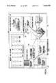
- FIG. 1(A and B)is an exploded perspective view showing the installation of a wafer made in accordance with the teachings of the preferred embodiment of this invention
- FIG. 2is a cross-sectional view of one embodiment of the invention in which the wafer is sandwiched between mated male and female connectors;
- FIG. 3is a partial cross-sectional view illustrating another embodiment and one technique for making electrical contact between the pins and the wafer;
- FIG. 4is a plan view of a suitable contact configuration
- FIG. 5is a partial side view showing the contact design in use
- FIG. 6(A and B)is a plan view illustrating one particular circuit design for the wafer
- FIG. 7is a side view of the wafer of FIG. 6.
- FIG. 8is a block diagram view of a system which may be used to test the wafers.
- a wafer 10is provided for making electrical connection to the pins 12 of a male electrical connector 14.
- Male electrical connector 14mates with a female connector 16 in a manner well known in the art.
- the male/female connectors 14 and 16are of the type meeting military specification (C-38999).
- the male connectoris characterized by a cylindrical metal outer shell 18 which is removably connected to a complementary metal shell 20 on the female connector 16.
- the removable connectionis usually made by a bayonet coupling on the mating surfaces of the shells 18 and 20, although other such connections can also be made to ensure proper mating of the connectors.
- the interior of the male connectorincludes a nonconductive insert 22 that maintains the orientation of the pins 12 and insulates them from the conductive shell 18.
- the female connector 16likewise includes a nonconductive insert 24 and an array of sockets 26 for receiving the pins 12.
- the male connectoris shown in FIG. 1 as being coupled to electronic equipment 28.
- the female connector 16is mounted on one end of an electrical cable 30.
- the cablecontains a plurality of wires that carry electrical signals to and from the electronic equipment 28 when the
- connectors 14 and 16are mated together.
- the wafer 10is inserted between the mated connectors 14 and 16.
- the wafer 10has a diameter smaller than the inner diameter of the smallest connector shell and is thin enough to be inserted between the connector pair without interfering with the positive connection therebetween.
- wafer 10includes two generally parallel major surfaces 32 and 34, along with a peripheral edge 36.
- a series of holes 38are formed between the two major faces of the wafer. Holes 38 are aligned with and slightly larger than the diameter of pins 12.
- Circuitryis formed on the wafer 10 and is in electrical contact with one or more of the pins 12.
- the circuitry 40can be any of a wide variety of devices such as active and passive electronic components, as well as more sophisticated microprocessing circuitry.
- the circuitry 40is generally designed to perform preselected functions associated with the electrical signals on the pins 12. These functions include, but are not limited to, radio frequency instrumentation, signal rerouting and interface protection using passive electronic components such as current/voltage monitors, transient limiters and point-to-point wiring.
- Active electronicssuch as analog and logic circuitry, matrix switches, power management devices and temperature/shock sensors can be utilized to provide discrete event monitoring, integrated built-in test augmentation and diagnostics, signal processing, interface diagnostics and/or signal conditioning.
- Circuitry 40may take the form of microprocessing circuitry such as the 68000 variety, and may include static RAM and ROM as well as non-volatile memory. In that event, the circuitry can provide discrete event recordation and decision based signal conditioning/diagnostics.
- Circuitry 40is shown in FIG. 6, however, as consisting simply of a plurality of fuses 40(a, b, and c) which are formed by areas of reduced widths in a thin film metal layer 42 formed on surface 32 of wafer 10.
- the fuses 40(a, b and c)are connected to the pins and operate, in this example, to sense electromagnetic pulse induced stress on the pins 12. If, for example, a potentially damaging pulse is received exceeding a predetermined current level then one or more of the fuses will melt causing a change in resistance associated with that pin.
- the waferin this example, takes the form of a silicon substrate 41 and includes a passivation layer 46, as shown in FIG. 7.
- the circuitry 40being a simple metal fuse formed on the wafer surface, conventional very large scale integration circuit techniques can be used to form active devices within the body of the semiconductor wafer.
- each metallic disc 50is provided for each wafer hole 38.
- each metallic disc 50includes an aperture 52 whose diameter is slightly smaller than the cross sectional diameter of the connector pin 12.
- a plurality of radially extending slits 54define an array of bendable fingers 56, the inner portions of which serve to bend under the force of the connector pin being inserted through the wafer holes 38 to thereby make a sliding, removable, yet positive electrical connection with each pin.
- the non-slitted peripheral rim 58 of the disc 50is mounted by way of conductive epoxy or solder to conductive circular pads 60 on wafer 10 surrounding holes 38.
- the discs 50are connected by way of metal traces 42 to the circuitry which, in FIG. 5, bears the reference numeral 40' to represent an active electronic integrated circuit component formed in the surface of semiconductor material serving as wafer 10.
- FIG. 2illustrates a somewhat more sophisticated embodiment where bidirectional communication is made between the circuitry 40 on the wafer 10.
- the waferincludes a suitable onboard optical transceiver 64 which communicates with a remote transceiver and converter 66 via a light waveguide 68.
- Transceiver and converter 66is coupled to a suitable controller 70 which may be provided by way of a host computer. Electrical signals from the controller 70 are converted by transceiver/converter 66 into suitable light pulses which are transmitted by waveguide 68 to the transceiver 64 on wafer 10.
- the waveguide 68can be made of suitable material that has sufficient flexibility and integrity to transmit the optical information in a reliable manner.
- Waveguide 68can, for example, take the form of a Mylar strip which is preferably coated with a reflecting substance on its outer surfaces to increase the efficiency of the optical transmission.
- Optical transceiver 64converts the optical signal from waveguide 68 into suitable electrical signals which are fed to the circuitry 40 on the wafer 10.
- the signalscould be used to program a suitable integrated circuit microprocessor which serves as the circuitry 40.
- the microprocessorthen could communicate with the electronic equipment 28 via the pins 12 in the male connector 14 (FIG. 1).
- signals from the electronic equipment 28can be communicated to the remote controller 70 via the pins 12, circuitry 40, optical transceiver 64, waveguide 68 and optical transceiver/converter 66.
- a system of this typecan be used for a variety of applications such as advanced signal processing, intelligent instrumentation, real-time data stream monitoring, remotely controlled signal conditioning, switching and processing; remotely controlled interface diagnostics, transient data recordation and the like. Again, these applications are by way of non-limiting examples.
- the circuitrytakes the form of the fuses shown in FIGS. 6 and 7, it would be desirable to periodically remove and test the wafer to determine if any of the fuses 40(a, b, c) had melted due to high levels of electromagnetic induced current pulses on the pins 12.
- FIG. 8illustrates a suitable test console 70 for this purpose.
- Console 70includes a wafer identification unit 72, a wafer test fixture 74, a switching matrix 76, measurement circuitry 78, threshold verification circuitry 80 and computer control 82.
- the identification unit 72uniquely identifies a wafer 10 by means of an identification tag 84 on each wafer 10.
- Tag 84in this example, is a conventional bar code which can be read by a suitable bar code reader 86.
- a wafer extraction tool 88aids in the insertion and removal of the wafer into the connector 14 and minimizes the risk of wafer damage due to mechanical stress or other events.
- Tool 88employs a vacuum system 90 with a vacuum head 92 designed to temporarily hold the wafer 10.
- the head 92manipulates the wafer so that the pins slide into the wafer holes 38 and make electrical connection to the pin contacts 50 and the shell contacts 62 make connection to the shell 18 (FIG. 3).
- the male and female connectors 14 and 16are then mated together in the usual manner with the pins 12 being inserted into the female sockets 26.
- the wafer 10is sufficiently thin that it does not disturb the normal mating of the connectors.
- the connectorsare disassembled and the vacuum tool 88 is used to extract the wafer 10 from the male connector 14.
- the wafersthen are placed in the test fixture 74 which generally consists of a bank of the same MIL-SPEC connectors 14.
- the test fixture 74is capable of testing one wafer at a time by placing the wafer in its corresponding connector.
- An LED indicator 94automatically locates the proper connector to use based on the wafer's identification code.
- the switching matrix 76switches the resistance measurement between any pin on the connector and another pin or the connector shell. It also switches in an onboard switched DC power supply to verify the threshold of any of the fuses 40(a, b or c).
- the switching matrix 76is controlled by the computer 82 through a bus interface card.
- the measurement circuitry 78makes a resistance measurement that determines which fuses 40(a, b or c), if any, have been blown.
- the threshold verification circuitry 80includes a programmable switch DC power supply and a source resistant network. It creates a known square pulse with enough amplitude to blow any of the fuses. The pulse level is stepped up slowly and the fuse resistance is read after each pulse to determine when the fuse blows and what its threshold was.
- Computer control 82controls all of the systems and records the data from the test. The computer is suitably programmed so that it will control all the testing procedure.
Landscapes
- Engineering & Computer Science (AREA)
- Microelectronics & Electronic Packaging (AREA)
- Theoretical Computer Science (AREA)
- Computer Security & Cryptography (AREA)
- Physics & Mathematics (AREA)
- Power Engineering (AREA)
- Software Systems (AREA)
- General Physics & Mathematics (AREA)
- General Engineering & Computer Science (AREA)
- Computer Hardware Design (AREA)
- Electromagnetism (AREA)
- Tests Of Electronic Circuits (AREA)
- Measuring Leads Or Probes (AREA)
- Photo Coupler, Interrupter, Optical-To-Optical Conversion Devices (AREA)
- Testing Or Measuring Of Semiconductors Or The Like (AREA)
- Coupling Device And Connection With Printed Circuit (AREA)
- Details Of Connecting Devices For Male And Female Coupling (AREA)
Abstract
Description
Claims (34)
Priority Applications (15)
| Application Number | Priority Date | Filing Date | Title |
|---|---|---|---|
| US07/895,148US5181859A (en) | 1991-04-29 | 1992-06-05 | Electrical connector circuit wafer |
| US07/938,111US5290191A (en) | 1991-04-29 | 1992-08-31 | Interface conditioning insert wafer |
| CA002077486ACA2077486C (en) | 1992-06-05 | 1992-09-03 | Electrical connector circuit wafer |
| TW081107473ATW209312B (en) | 1992-06-05 | 1992-09-22 | |
| DE69215215TDE69215215T2 (en) | 1992-06-05 | 1992-09-22 | Integrated semiconductor circuit board of an electrical connector |
| EP92308603AEP0573714B1 (en) | 1992-06-05 | 1992-09-22 | Electrical connector circuit wafer |
| JP25303392AJPH0715957B2 (en) | 1992-06-05 | 1992-09-22 | Electrical connector circuit wafer |
| KR1019920023273AKR0162907B1 (en) | 1992-06-05 | 1992-12-04 | Electrical connector circuit wafer |
| US07/998,333US5414587A (en) | 1991-04-29 | 1992-12-30 | Surge suppression device |
| US08/054,658US5387131A (en) | 1991-04-29 | 1993-04-23 | Network conditioning insert |
| US08/087,638US5455734A (en) | 1991-04-29 | 1993-07-01 | Insert device for electrical relays, solenoids, motors, controllers, and the like |
| US08/262,410US5428288A (en) | 1991-04-29 | 1994-06-20 | Microelectric monitoring device |
| US08/394,924US5590058A (en) | 1991-04-29 | 1995-02-24 | Battery monitor for unobstrusive installation with a battery connector |
| US08/520,497US5568348A (en) | 1991-04-29 | 1995-08-29 | Insert device for electrical relays, solenoids, motors, controllers, and the like |
| US08/631,601US5692917A (en) | 1991-04-29 | 1996-04-18 | Computer hardware insert device for software authorization |
Applications Claiming Priority (2)
| Application Number | Priority Date | Filing Date | Title |
|---|---|---|---|
| US69426291A | 1991-04-29 | 1991-04-29 | |
| US07/895,148US5181859A (en) | 1991-04-29 | 1992-06-05 | Electrical connector circuit wafer |
Related Parent Applications (2)
| Application Number | Title | Priority Date | Filing Date |
|---|---|---|---|
| US69426291AContinuation | 1991-04-29 | 1991-04-29 | |
| US69426291AContinuation-In-Part | 1991-04-29 | 1991-04-29 |
Related Child Applications (1)
| Application Number | Title | Priority Date | Filing Date |
|---|---|---|---|
| US07/938,111Continuation-In-PartUS5290191A (en) | 1991-04-29 | 1992-08-31 | Interface conditioning insert wafer |
Publications (1)
| Publication Number | Publication Date |
|---|---|
| US5181859Atrue US5181859A (en) | 1993-01-26 |
Family
ID=25404075
Family Applications (2)
| Application Number | Title | Priority Date | Filing Date |
|---|---|---|---|
| US07/895,148Expired - LifetimeUS5181859A (en) | 1991-04-29 | 1992-06-05 | Electrical connector circuit wafer |
| US07/938,111Expired - LifetimeUS5290191A (en) | 1991-04-29 | 1992-08-31 | Interface conditioning insert wafer |
Family Applications After (1)
| Application Number | Title | Priority Date | Filing Date |
|---|---|---|---|
| US07/938,111Expired - LifetimeUS5290191A (en) | 1991-04-29 | 1992-08-31 | Interface conditioning insert wafer |
Country Status (7)
| Country | Link |
|---|---|
| US (2) | US5181859A (en) |
| EP (1) | EP0573714B1 (en) |
| JP (1) | JPH0715957B2 (en) |
| KR (1) | KR0162907B1 (en) |
| CA (1) | CA2077486C (en) |
| DE (1) | DE69215215T2 (en) |
| TW (1) | TW209312B (en) |
Cited By (95)
| Publication number | Priority date | Publication date | Assignee | Title |
|---|---|---|---|---|
| GB2274030A (en)* | 1992-12-30 | 1994-07-06 | Trw Inc | Surge suppresion device |
| US5355276A (en)* | 1992-07-16 | 1994-10-11 | Chal Ming Kuang | Network connector for computer |
| US5387131A (en)* | 1991-04-29 | 1995-02-07 | Trw Inc. | Network conditioning insert |
| GB2283866A (en)* | 1993-11-08 | 1995-05-17 | Lozano Rico Santiago | Through adaptor connector containing circuitry |
| US5428288A (en)* | 1991-04-29 | 1995-06-27 | Trw Inc. | Microelectric monitoring device |
| GB2286085A (en)* | 1993-11-02 | 1995-08-02 | Rico Santiago Lozano | Base connector/module for a relay |
| US5455734A (en)* | 1991-04-29 | 1995-10-03 | Trw Inc. | Insert device for electrical relays, solenoids, motors, controllers, and the like |
| US5467526A (en)* | 1993-11-22 | 1995-11-21 | E-Systems, Inc. | Tool for wafer alignment and insertion |
| US5554050A (en)* | 1995-03-09 | 1996-09-10 | The Whitaker Corporation | Filtering insert for electrical connectors |
| US5572409A (en)* | 1994-02-08 | 1996-11-05 | Prolinx Labs Corporation | Apparatus including a programmable socket adapter for coupling an electronic component to a component socket on a printed circuit board |
| US5590058A (en)* | 1991-04-29 | 1996-12-31 | Trw Inc. | Battery monitor for unobstrusive installation with a battery connector |
| US5615824A (en)* | 1994-06-07 | 1997-04-01 | Tessera, Inc. | Soldering with resilient contacts |
| US5632631A (en)* | 1994-06-07 | 1997-05-27 | Tessera, Inc. | Microelectronic contacts with asperities and methods of making same |
| US5686697A (en)* | 1995-01-06 | 1997-11-11 | Metatech Corporation | Electrical circuit suspension system |
| US5692917A (en)* | 1991-04-29 | 1997-12-02 | Trw Inc. | Computer hardware insert device for software authorization |
| US5726482A (en) | 1994-02-08 | 1998-03-10 | Prolinx Labs Corporation | Device-under-test card for a burn-in board |
| US5767575A (en) | 1995-10-17 | 1998-06-16 | Prolinx Labs Corporation | Ball grid array structure and method for packaging an integrated circuit chip |
| US5802699A (en)* | 1994-06-07 | 1998-09-08 | Tessera, Inc. | Methods of assembling microelectronic assembly with socket for engaging bump leads |
| US5808351A (en) | 1994-02-08 | 1998-09-15 | Prolinx Labs Corporation | Programmable/reprogramable structure using fuses and antifuses |
| US5810609A (en)* | 1995-08-28 | 1998-09-22 | Tessera, Inc. | Socket for engaging bump leads on a microelectronic device and methods therefor |
| US5813881A (en) | 1994-02-08 | 1998-09-29 | Prolinx Labs Corporation | Programmable cable and cable adapter using fuses and antifuses |
| US5834824A (en) | 1994-02-08 | 1998-11-10 | Prolinx Labs Corporation | Use of conductive particles in a nonconductive body as an integrated circuit antifuse |
| US5872338A (en) | 1996-04-10 | 1999-02-16 | Prolinx Labs Corporation | Multilayer board having insulating isolation rings |
| US5895432A (en)* | 1995-08-02 | 1999-04-20 | Snap-On Incorporated | Method and apparatus for simultaneously coupling plural terminal devices through serial port and remote control apparatus incorporating same |
| US5906042A (en) | 1995-10-04 | 1999-05-25 | Prolinx Labs Corporation | Method and structure to interconnect traces of two conductive layers in a printed circuit board |
| US5906043A (en) | 1995-01-18 | 1999-05-25 | Prolinx Labs Corporation | Programmable/reprogrammable structure using fuses and antifuses |
| US5909350A (en)* | 1997-04-08 | 1999-06-01 | X2Y Attenuators, L.L.C. | Paired multi-layered dielectric independent passive component architecture resulting in differential and common mode filtering with surge protection in one integrated package |
| US5917229A (en) | 1994-02-08 | 1999-06-29 | Prolinx Labs Corporation | Programmable/reprogrammable printed circuit board using fuse and/or antifuse as interconnect |
| US5983492A (en)* | 1996-11-27 | 1999-11-16 | Tessera, Inc. | Low profile socket for microelectronic components and method for making the same |
| US6013358A (en)* | 1997-11-18 | 2000-01-11 | Cooper Industries, Inc. | Transient voltage protection device with ceramic substrate |
| US6018448A (en)* | 1997-04-08 | 2000-01-25 | X2Y Attenuators, L.L.C. | Paired multi-layered dielectric independent passive component architecture resulting in differential and common mode filtering with surge protection in one integrated package |
| US6034427A (en) | 1998-01-28 | 2000-03-07 | Prolinx Labs Corporation | Ball grid array structure and method for packaging an integrated circuit chip |
| US6097581A (en)* | 1997-04-08 | 2000-08-01 | X2Y Attenuators, Llc | Paired multi-layered dielectric independent passive component architecture resulting in differential and common mode filtering with surge protection in one integrated package |
| US6139345A (en)* | 1999-10-18 | 2000-10-31 | Itt Manufacturing Enterprises, Inc. | Clip for coupling component to connector contacts |
| CN1073751C (en)* | 1994-04-28 | 2001-10-24 | Trw公司 | Surge suppression device |
| US20010048581A1 (en)* | 1997-04-08 | 2001-12-06 | X2Y Attenuators, L.L.C. | Predetermined symmetrically balanced amalgam with complementary paired portions comprising shielding electrodes and shielded electrodes and other predetermined element portions for symmetrically balanced and complementary energy portion conditioning |
| US6373673B1 (en) | 1997-04-08 | 2002-04-16 | X2Y Attenuators, Llc | Multi-functional energy conditioner |
| US6407542B1 (en)* | 2000-03-23 | 2002-06-18 | Avaya Technology Corp. | Implementation of a multi-port modal decomposition system |
| US20020158515A1 (en)* | 1997-04-08 | 2002-10-31 | Anthony Anthony A. | Offset pathway arrangements for energy conditioning |
| US6498710B1 (en) | 1997-04-08 | 2002-12-24 | X2Y Attenuators, Llc | Paired multi-layered dielectric independent passive component architecture resulting in differential and common mode filtering with surge protection in one integrated package |
| US20030029635A1 (en)* | 1997-04-08 | 2003-02-13 | Anthony Anthony A. | Pathway arrangement |
| US20030067730A1 (en)* | 1997-04-08 | 2003-04-10 | Anthony Anthony A. | Universial energy conditioning interposer with circuit architecture |
| US6603646B2 (en) | 1997-04-08 | 2003-08-05 | X2Y Attenuators, Llc | Multi-functional energy conditioner |
| US6606011B2 (en) | 1998-04-07 | 2003-08-12 | X2Y Attenuators, Llc | Energy conditioning circuit assembly |
| US20030161086A1 (en)* | 2000-07-18 | 2003-08-28 | X2Y Attenuators, Llc | Paired multi-layered dielectric independent passive component architecture resulting in differential and common mode filtering with surge protection in one integrated package |
| US20030168917A1 (en)* | 2001-12-03 | 2003-09-11 | Ejaz Afzal | Dual input AC/DC power converter having a programmable peripheral power hub module |
| US6636406B1 (en) | 1997-04-08 | 2003-10-21 | X2Y Attenuators, Llc | Universal multi-functional common conductive shield structure for electrical circuitry and energy conditioning |
| US20030202312A1 (en)* | 2000-04-28 | 2003-10-30 | Anthony Anthony A. | Predetermined symmetrically balanced amalgam with complementary paired portions comprising shielding electrodes and shielded electrodes and other predetermined element portions for symmetrically balanced and complementary energy portion conditioning |
| US6643158B2 (en) | 2001-10-31 | 2003-11-04 | Mobility Electronics, Inc. | Dual input AC/DC to programmable DC output converter |
| US6650525B2 (en) | 1997-04-08 | 2003-11-18 | X2Y Attenuators, Llc | Component carrier |
| US6650560B2 (en) | 2001-12-03 | 2003-11-18 | Mobility Electronics, Inc. | Dual input AC and DC power supply having a programmable DC output utilizing single-loop optical feedback |
| US20030231456A1 (en)* | 2000-03-22 | 2003-12-18 | Anthony Anthony | Energy conditioning structure |
| US6687108B1 (en) | 1997-04-08 | 2004-02-03 | X2Y Attenuators, Llc | Passive electrostatic shielding structure for electrical circuitry and energy conditioning with outer partial shielded energy pathways |
| US6700808B2 (en) | 2002-02-08 | 2004-03-02 | Mobility Electronics, Inc. | Dual input AC and DC power supply having a programmable DC output utilizing a secondary buck converter |
| US20040050596A1 (en)* | 2000-12-12 | 2004-03-18 | Hiroshi Shimizu | Steering mechanism of electric car |
| US20040054426A1 (en)* | 2000-10-17 | 2004-03-18 | Anthony William M. | Energy pathway arrangement |
| US20040085793A1 (en)* | 2001-12-03 | 2004-05-06 | Ejaz Afzal | Programmable power converter |
| US20040085699A1 (en)* | 2000-10-17 | 2004-05-06 | Anthony William M. | Amalgam of shielding and shielded energy pathways and other elements for single or multiiple circuitries with common reference node |
| US6738249B1 (en) | 1997-04-08 | 2004-05-18 | X2Y Attenuators, Llc | Universal energy conditioning interposer with circuit architecture |
| US20040105205A1 (en)* | 2000-10-17 | 2004-06-03 | Anthony William M. | Energy pathway arrangement |
| US6751109B2 (en) | 2001-10-31 | 2004-06-15 | Mobility Electronics, Inc. | Dual input AC/DC/ battery operated power supply |
| US20040124949A1 (en)* | 1998-04-07 | 2004-07-01 | Anthony Anthony | Component carrier |
| US20040130840A1 (en)* | 2000-12-15 | 2004-07-08 | Anthony William M. | Energy pathway arrangements for energy conditioning |
| US20040218332A1 (en)* | 1997-04-08 | 2004-11-04 | Anthony Anthony A | Arrangement for energy conditioning |
| US20040226733A1 (en)* | 2003-01-31 | 2004-11-18 | David Anthony | Shielded energy conditioner |
| US6954346B2 (en) | 1997-04-08 | 2005-10-11 | Xzy Attenuators, Llc | Filter assembly |
| US7110235B2 (en) | 1997-04-08 | 2006-09-19 | Xzy Altenuators, Llc | Arrangement for energy conditioning |
| US7262949B2 (en) | 2000-08-15 | 2007-08-28 | X2Y Attenuators, Llc | Electrode arrangement for circuit energy conditioning |
| US7301748B2 (en) | 1997-04-08 | 2007-11-27 | Anthony Anthony A | Universal energy conditioning interposer with circuit architecture |
| US7321485B2 (en) | 1997-04-08 | 2008-01-22 | X2Y Attenuators, Llc | Arrangement for energy conditioning |
| US20080228231A1 (en)* | 2007-01-19 | 2008-09-18 | University Of Southern California | Acoustic Back-Scattering Sensing Screw for Preventing Spine Surgery Complications |
| US7427816B2 (en) | 1998-04-07 | 2008-09-23 | X2Y Attenuators, Llc | Component carrier |
| US20080248687A1 (en)* | 2005-03-01 | 2008-10-09 | Anthony William M | Internally Overlapped Conditioners |
| US7440252B2 (en) | 2003-05-29 | 2008-10-21 | X2Y Attenuators, Llc | Connector related structures including an energy conditioner |
| US7586728B2 (en) | 2005-03-14 | 2009-09-08 | X2Y Attenuators, Llc | Conditioner with coplanar conductors |
| US20090251149A1 (en)* | 2008-04-02 | 2009-10-08 | Eastway Fair Company Limited | Battery tester |
| US7675729B2 (en) | 2003-12-22 | 2010-03-09 | X2Y Attenuators, Llc | Internally shielded energy conditioner |
| US20100254162A1 (en)* | 2009-04-01 | 2010-10-07 | Comarco Wireless Technologies, Inc. | Modular power adapter |
| US7817397B2 (en) | 2005-03-01 | 2010-10-19 | X2Y Attenuators, Llc | Energy conditioner with tied through electrodes |
| US20110095605A1 (en)* | 2009-10-28 | 2011-04-28 | Comarco Wireless Technologies, Inc. | Power supply equipment to simultaneously power multiple electronic device |
| US8026777B2 (en) | 2006-03-07 | 2011-09-27 | X2Y Attenuators, Llc | Energy conditioner structures |
| WO2012045239A1 (en)* | 2010-10-08 | 2012-04-12 | Huawei Technologies Co., Ltd. | Electrical and mechanical connection |
| CN102544789A (en)* | 2010-12-28 | 2012-07-04 | 中山大洋电机股份有限公司 | A terminal connection device connected with a serial port socket |
| WO2013062780A1 (en)* | 2011-10-28 | 2013-05-02 | Apple Inc. | Split jack assemblies and methods for making the same |
| DE102013016550A1 (en)* | 2013-10-04 | 2015-04-23 | Leoni Bordnetz-Systeme Gmbh | Electrical coupling unit and sensor module configured for this purpose |
| US9054094B2 (en) | 1997-04-08 | 2015-06-09 | X2Y Attenuators, Llc | Energy conditioning circuit arrangement for integrated circuit |
| FR3022702A1 (en)* | 2014-06-24 | 2015-12-25 | Hypertac Sa | ELECTRICAL CONNECTOR FORMING A SOCKET OR PLUG, ASSEMBLY AND INSTALLATION COMPRISING SUCH A CONNECTOR |
| US9478887B2 (en) | 2013-11-01 | 2016-10-25 | Quell Corporation | Flexible electrical connector insert with conductive and non-conductive elastomers |
| DE102015106251A1 (en)* | 2015-04-23 | 2016-10-27 | Phoenix Contact E-Mobility Gmbh | Connector part with a temperature monitoring device |
| US9692188B2 (en) | 2013-11-01 | 2017-06-27 | Quell Corporation | Flexible electrical connector insert with conductive and non-conductive elastomers |
| EP3157103A3 (en)* | 2012-07-31 | 2017-08-23 | St. Jude Medical Atrial Fibrillation Division Inc. | Magnetic field-compatible connector using magnetic noise cancelation loops |
| WO2018001719A1 (en)* | 2016-06-30 | 2018-01-04 | Phoenix Contact E-Mobility Gmbh | Electrical connection device with thermal coupling to a printed circuit board which has a temperature sensor |
| US10855086B2 (en) | 2004-01-15 | 2020-12-01 | Comarco Wireless Systems Llc | Power supply equipment utilizing interchangeable tips to provide power and a data signal to electronic devices |
| US10931069B2 (en) | 2018-04-30 | 2021-02-23 | Atl Technology, Llc | High-density electrical connector |
| US12407123B1 (en) | 2020-11-23 | 2025-09-02 | Quell Corporation | Electrically dissipative flexible unitary connector insert |
Families Citing this family (50)
| Publication number | Priority date | Publication date | Assignee | Title |
|---|---|---|---|---|
| US5683256A (en)* | 1994-12-09 | 1997-11-04 | Methode Electronics, Inc. | Integral thru-hole contacts |
| US5625299A (en)* | 1995-02-03 | 1997-04-29 | Uhling; Thomas F. | Multiple lead analog voltage probe with high signal integrity over a wide band width |
| US5660567A (en)* | 1995-11-14 | 1997-08-26 | Nellcor Puritan Bennett Incorporated | Medical sensor connector with removable encoding device |
| US6081109A (en)* | 1997-11-07 | 2000-06-27 | Xantech Corporation | Current sensing device |
| US6218806B1 (en) | 1998-06-03 | 2001-04-17 | Black & Decker Inc. | Method and apparatus for obtaining product use information |
| US6254403B1 (en) | 1999-07-30 | 2001-07-03 | Litton Systems, Inc. | Assembly for and method of selectively grounding contacts of a connector to a rear portion of the connector |
| US6386913B1 (en)* | 2000-08-14 | 2002-05-14 | Fci Usa, Inc. | Electrical connector for micro co-axial conductors |
| US6555754B2 (en)* | 2001-01-18 | 2003-04-29 | Walbro Corporation | Automotive fuel tank electrical fitting |
| US20030016738A1 (en)* | 2001-07-18 | 2003-01-23 | Boolos Timothy L. | Testing system and method of non-invasive testing |
| TW504815B (en)* | 2001-11-16 | 2002-10-01 | Advanced Semiconductor Eng | Packaging mold device with ESD protection |
| JP3878041B2 (en)* | 2002-03-22 | 2007-02-07 | 株式会社日本マイクロニクス | Contact and electrical connection device using the same |
| US7136393B2 (en)* | 2002-07-19 | 2006-11-14 | Northrop Grumman Coporation | Information transmission system and method of data transmission |
| US20050010341A1 (en)* | 2002-09-20 | 2005-01-13 | Bendix Commercial Vehicle Systems Llc | Remote diagnostics device (rdu) |
| US6863544B2 (en)* | 2002-11-27 | 2005-03-08 | Bendix Commercial Vehicle Systems Llc | Remote diagnostic unit enclosure assembly |
| US7869974B2 (en) | 2003-01-15 | 2011-01-11 | Plishner Paul J | Connector or other circuit element having an indirectly coupled integrated circuit |
| US8159958B1 (en)* | 2004-04-06 | 2012-04-17 | At&T Intellectual Property Ii, L.P. | Krone block dongle |
| US6837747B1 (en) | 2004-04-19 | 2005-01-04 | Itt Manufacturing Enterprises, Inc. | Filtered connector |
| US7274977B2 (en)* | 2004-05-19 | 2007-09-25 | Bendix Commercial Vehicle Systems Llc | Feature enabling unit |
| FR2881584B1 (en)* | 2005-02-03 | 2007-04-27 | Souriau Soc Par Actions Simpli | MODULE FOR ASSEMBLING TWO CONNECTION ASSEMBLIES |
| US20060235586A1 (en)* | 2005-04-19 | 2006-10-19 | Waszkowski Paul J | Diagnostic device |
| US7297002B2 (en)* | 2005-07-27 | 2007-11-20 | Physical Optics Corporation | Stacked rotary connector assembly using a split ring configuration |
| US7462035B2 (en)* | 2005-07-27 | 2008-12-09 | Physical Optics Corporation | Electrical connector configured as a fastening element |
| DE102006055619A1 (en)* | 2006-11-24 | 2008-05-29 | Magna Powertrain Ag & Co Kg | Electrical plug connector part for connecting electrically controllable component at control unit of motor vehicle, has pins formed at openings of plate, which has circuit for fixing component, where circuit is connected with sections |
| KR101244954B1 (en)* | 2007-01-30 | 2013-03-18 | 엘지디스플레이 주식회사 | Back light unit and liquid crystal display device having the same |
| JP2008293747A (en) | 2007-05-23 | 2008-12-04 | Yazaki Corp | Communication relay device and relay connector unit |
| US8308489B2 (en)* | 2008-10-27 | 2012-11-13 | Physical Optics Corporation | Electrical garment and electrical garment and article assemblies |
| US8092234B2 (en)* | 2008-10-30 | 2012-01-10 | Deutsch Engineered Connecting Devices, Inc. | System and method for sensing information that is being communicated through a connector |
| US8063307B2 (en) | 2008-11-17 | 2011-11-22 | Physical Optics Corporation | Self-healing electrical communication paths |
| US8053683B2 (en)* | 2009-03-30 | 2011-11-08 | Lockheed Martin Corporation | Equipment container retention and bonding system and method |
| EP2262060A1 (en)* | 2009-06-10 | 2010-12-15 | Peter Weber | Grounding system for grounding a container |
| KR101063396B1 (en)* | 2009-10-30 | 2011-09-07 | 한국단자공업 주식회사 | Automotive Capacitor Connectors |
| FR2959623B1 (en)* | 2010-04-30 | 2013-03-15 | Souriau | DEVICE FOR COUPLING AN ASYNCHRONOUS MOTOR TO AN ELECTRIC POWER CABLE, AN ASYNCHRONOUS MOTOR, AND METHOD OF COUPLING AN ASYNCHRONOUS MOTOR TO AN ELECTRIC POWER CABLE |
| TWI429147B (en)* | 2011-06-21 | 2014-03-01 | Wistron Corp | Plug assembly adapted to an adapter and a computer device |
| US9240644B2 (en)* | 2012-08-22 | 2016-01-19 | Amphenol Corporation | High-frequency electrical connector |
| US9406462B2 (en)* | 2013-06-28 | 2016-08-02 | The Boeing Company | Truss interconnect |
| US20160204554A1 (en)* | 2014-02-28 | 2016-07-14 | Hitachi Metals, Ltd. | Connector and cable with connector |
| JP6323499B2 (en)* | 2016-06-20 | 2018-05-16 | 住友電気工業株式会社 | Coaxial cable with substrate and manufacturing method thereof |
| KR102123992B1 (en)* | 2018-07-16 | 2020-06-17 | (주)볼카텍 | Circuit changing device inserted in connector |
| US11745840B1 (en)* | 2019-09-12 | 2023-09-05 | The United States Of America As Represented By The Secretary Of The Navy | Apparatus and method for joining modules in a field configurable autonomous vehicle |
| US11541801B1 (en) | 2019-09-12 | 2023-01-03 | The United States Of America As Represented By The Secretary Of The Navy | Method and apparatus for positioning the center of mass on an unmanned underwater vehicle |
| US11904993B1 (en) | 2019-09-12 | 2024-02-20 | The United States Of America As Represented By The Secretary Of The Navy | Supplemental techniques for vehicle and module thermal management |
| US11505283B1 (en) | 2019-09-12 | 2022-11-22 | The United States Of America As Represented By The Secretary Of The Navy | Apparatus for coupling and positioning elements on a configurable vehicle |
| US11511836B1 (en) | 2019-09-12 | 2022-11-29 | The United States Of America As Represented By The Secretary Of The Navy | Field configurable spherical underwater vehicle |
| US12244352B1 (en) | 2019-09-12 | 2025-03-04 | The United States Of America As Represented By The Secretary Of The Navy | Optical communications for autonomous vehicles |
| US11530017B1 (en) | 2019-09-12 | 2022-12-20 | The United States Of America As Represented By The Secretary Of The Navy | Scuttle module for field configurable vehicle |
| US11530019B1 (en) | 2019-09-12 | 2022-12-20 | The United States Of America As Represented By The Secretary Of The Navy | Propulsion system for field configurable vehicle |
| US11760454B1 (en) | 2019-09-12 | 2023-09-19 | The United States Of America As Represented By The Secretary Of The Navy | Methods of forming field configurable underwater vehicles |
| US11505296B1 (en) | 2019-09-12 | 2022-11-22 | The United States Of America As Represented By The Secretary Of The Navy | Method and apparatus for transporting ballast and cargo in an autonomous vehicle |
| US11608149B1 (en) | 2019-09-12 | 2023-03-21 | The United States Of America As Represented By The Secretary Of The Navy | Buoyancy control module for field configurable autonomous vehicle |
| US11603170B1 (en) | 2019-10-03 | 2023-03-14 | The United States Of America As Represented By The Secretary Of The Navy | Method for parasitic transport of an autonomous vehicle |
Citations (31)
| Publication number | Priority date | Publication date | Assignee | Title |
|---|---|---|---|---|
| US2073880A (en)* | 1935-06-19 | 1937-03-16 | Solar Mfg Corp | Interference eliminating device |
| US2760128A (en)* | 1954-11-03 | 1956-08-21 | Collins Radio Co | Grid terminal pick-up plate |
| US2944330A (en)* | 1955-11-08 | 1960-07-12 | Illinois Tool Works | Terminal clip structure and method and apparatus for applying same |
| US3072873A (en)* | 1960-06-20 | 1963-01-08 | Albert D Traher | Electrical plug adaptor |
| US3500194A (en)* | 1965-06-21 | 1970-03-10 | Devenco Inc | Method and means for detecting unauthorized use of electric power |
| US3569915A (en)* | 1968-09-16 | 1971-03-09 | Itt | Grounding foil |
| US3670292A (en)* | 1970-01-29 | 1972-06-13 | Itt | Grounding foil for electrical connectors |
| US3736379A (en)* | 1971-10-08 | 1973-05-29 | Western Electric Co | Inductive data coupler |
| US3753261A (en)* | 1971-12-09 | 1973-08-14 | K Thaxton | Continuous ground and polarity monitor |
| US3825874A (en)* | 1973-07-05 | 1974-07-23 | Itt | Electrical connector |
| US3852700A (en)* | 1969-04-18 | 1974-12-03 | Breston M | Grounding base for connector |
| US3905013A (en)* | 1973-04-27 | 1975-09-09 | Lee Maw Huei | Headlight warning system |
| UST947007I4 (en)* | 1975-01-23 | 1976-06-01 | ||
| US4002397A (en)* | 1975-09-29 | 1977-01-11 | Wolsk Associates, Ltd. | Connector for electric plug |
| US4056299A (en)* | 1976-05-03 | 1977-11-01 | Burroughs Corporation | Electrical connector |
| US4082394A (en)* | 1977-01-03 | 1978-04-04 | International Business Machines Corporation | Metallized ceramic and printed circuit module |
| US4326765A (en)* | 1980-04-15 | 1982-04-27 | International Telephone And Telegraph Corporation | Electronic device carrier |
| US4362350A (en)* | 1980-06-09 | 1982-12-07 | International Telephone And Telegraph Corporation | Contact retention assembly |
| US4407552A (en)* | 1978-05-18 | 1983-10-04 | Matsushita Electric Industrial Co., Ltd. | Connector unit |
| US4415218A (en)* | 1981-02-17 | 1983-11-15 | Rockwell International Corporation | Spring loaded diode contact apparatus |
| US4440463A (en)* | 1981-10-26 | 1984-04-03 | The Bendix Corporation | Electrical connector having a metallized plastic grounding insert |
| US4673237A (en)* | 1985-10-28 | 1987-06-16 | Gte Communication Systems Corporation | Connector filter adapter |
| US4676564A (en)* | 1985-10-28 | 1987-06-30 | Burroughs Corporation | Access device unit for installed pin grid array |
| US4717349A (en)* | 1985-10-10 | 1988-01-05 | Creek Electronics, Inc. | Electrical grounding accessory |
| US4820174A (en)* | 1986-08-06 | 1989-04-11 | Amp Incorporated | Modular connector assembly and filtered insert therefor |
| US4846705A (en)* | 1985-04-09 | 1989-07-11 | The Grass Valley Group, Inc. | Backplan connector |
| US4979070A (en)* | 1989-06-13 | 1990-12-18 | Bodkin Lawrence E | Automatic reset circuit for GFCI |
| US4979904A (en)* | 1990-01-16 | 1990-12-25 | Litton Systems, Inc. | Grounding disc |
| US5092788A (en)* | 1990-12-03 | 1992-03-03 | Motorola, Inc. | Self-contained universal accessory connector and seal |
| US5118302A (en)* | 1991-06-03 | 1992-06-02 | Ornamotor, Inc. | Electrical connector |
| US5134252A (en)* | 1990-01-21 | 1992-07-28 | Sony Corporation | Signal line |
Family Cites Families (8)
| Publication number | Priority date | Publication date | Assignee | Title |
|---|---|---|---|---|
| US3271726A (en)* | 1961-11-02 | 1966-09-06 | Bendix Corp | Electrical connector |
| US3086188A (en)* | 1962-01-18 | 1963-04-16 | Joseph I Ross | Non-reversing hermaphroditic cable connectors |
| US3718859A (en)* | 1971-02-01 | 1973-02-27 | Us Army | Electric circuit test element for use with a pair of electrical connectors |
| AU3655584A (en)* | 1984-01-03 | 1985-07-11 | Amp Incorporated | Active electrical connector |
| DE8428300U1 (en)* | 1984-09-26 | 1985-02-07 | Wilo-Werk Gmbh & Co Pumpen- Und Apparatebau, 4600 Dortmund | Device for switching an electric motor |
| US4813891A (en)* | 1987-07-22 | 1989-03-21 | G & H Technology, Inc. | Electrical connector for diverting EMP |
| EP0348562B1 (en)* | 1988-06-28 | 1993-06-16 | Trw Inc. | High-density contact area electrical connectors |
| US4992333A (en)* | 1988-11-18 | 1991-02-12 | G&H Technology, Inc. | Electrical overstress pulse protection |
- 1992
- 1992-06-05USUS07/895,148patent/US5181859A/ennot_activeExpired - Lifetime
- 1992-08-31USUS07/938,111patent/US5290191A/ennot_activeExpired - Lifetime
- 1992-09-03CACA002077486Apatent/CA2077486C/ennot_activeExpired - Lifetime
- 1992-09-22DEDE69215215Tpatent/DE69215215T2/ennot_activeExpired - Lifetime
- 1992-09-22JPJP25303392Apatent/JPH0715957B2/ennot_activeExpired - Lifetime
- 1992-09-22TWTW081107473Apatent/TW209312B/zhnot_activeIP Right Cessation
- 1992-09-22EPEP92308603Apatent/EP0573714B1/ennot_activeExpired - Lifetime
- 1992-12-04KRKR1019920023273Apatent/KR0162907B1/ennot_activeExpired - Lifetime
Patent Citations (31)
| Publication number | Priority date | Publication date | Assignee | Title |
|---|---|---|---|---|
| US2073880A (en)* | 1935-06-19 | 1937-03-16 | Solar Mfg Corp | Interference eliminating device |
| US2760128A (en)* | 1954-11-03 | 1956-08-21 | Collins Radio Co | Grid terminal pick-up plate |
| US2944330A (en)* | 1955-11-08 | 1960-07-12 | Illinois Tool Works | Terminal clip structure and method and apparatus for applying same |
| US3072873A (en)* | 1960-06-20 | 1963-01-08 | Albert D Traher | Electrical plug adaptor |
| US3500194A (en)* | 1965-06-21 | 1970-03-10 | Devenco Inc | Method and means for detecting unauthorized use of electric power |
| US3569915A (en)* | 1968-09-16 | 1971-03-09 | Itt | Grounding foil |
| US3852700A (en)* | 1969-04-18 | 1974-12-03 | Breston M | Grounding base for connector |
| US3670292A (en)* | 1970-01-29 | 1972-06-13 | Itt | Grounding foil for electrical connectors |
| US3736379A (en)* | 1971-10-08 | 1973-05-29 | Western Electric Co | Inductive data coupler |
| US3753261A (en)* | 1971-12-09 | 1973-08-14 | K Thaxton | Continuous ground and polarity monitor |
| US3905013A (en)* | 1973-04-27 | 1975-09-09 | Lee Maw Huei | Headlight warning system |
| US3825874A (en)* | 1973-07-05 | 1974-07-23 | Itt | Electrical connector |
| UST947007I4 (en)* | 1975-01-23 | 1976-06-01 | ||
| US4002397A (en)* | 1975-09-29 | 1977-01-11 | Wolsk Associates, Ltd. | Connector for electric plug |
| US4056299A (en)* | 1976-05-03 | 1977-11-01 | Burroughs Corporation | Electrical connector |
| US4082394A (en)* | 1977-01-03 | 1978-04-04 | International Business Machines Corporation | Metallized ceramic and printed circuit module |
| US4407552A (en)* | 1978-05-18 | 1983-10-04 | Matsushita Electric Industrial Co., Ltd. | Connector unit |
| US4326765A (en)* | 1980-04-15 | 1982-04-27 | International Telephone And Telegraph Corporation | Electronic device carrier |
| US4362350A (en)* | 1980-06-09 | 1982-12-07 | International Telephone And Telegraph Corporation | Contact retention assembly |
| US4415218A (en)* | 1981-02-17 | 1983-11-15 | Rockwell International Corporation | Spring loaded diode contact apparatus |
| US4440463A (en)* | 1981-10-26 | 1984-04-03 | The Bendix Corporation | Electrical connector having a metallized plastic grounding insert |
| US4846705A (en)* | 1985-04-09 | 1989-07-11 | The Grass Valley Group, Inc. | Backplan connector |
| US4717349A (en)* | 1985-10-10 | 1988-01-05 | Creek Electronics, Inc. | Electrical grounding accessory |
| US4676564A (en)* | 1985-10-28 | 1987-06-30 | Burroughs Corporation | Access device unit for installed pin grid array |
| US4673237A (en)* | 1985-10-28 | 1987-06-16 | Gte Communication Systems Corporation | Connector filter adapter |
| US4820174A (en)* | 1986-08-06 | 1989-04-11 | Amp Incorporated | Modular connector assembly and filtered insert therefor |
| US4979070A (en)* | 1989-06-13 | 1990-12-18 | Bodkin Lawrence E | Automatic reset circuit for GFCI |
| US4979904A (en)* | 1990-01-16 | 1990-12-25 | Litton Systems, Inc. | Grounding disc |
| US5134252A (en)* | 1990-01-21 | 1992-07-28 | Sony Corporation | Signal line |
| US5092788A (en)* | 1990-12-03 | 1992-03-03 | Motorola, Inc. | Self-contained universal accessory connector and seal |
| US5118302A (en)* | 1991-06-03 | 1992-06-02 | Ornamotor, Inc. | Electrical connector |
Cited By (191)
| Publication number | Priority date | Publication date | Assignee | Title |
|---|---|---|---|---|
| US5387131A (en)* | 1991-04-29 | 1995-02-07 | Trw Inc. | Network conditioning insert |
| US5414587A (en)* | 1991-04-29 | 1995-05-09 | Trw Inc. | Surge suppression device |
| US5590058A (en)* | 1991-04-29 | 1996-12-31 | Trw Inc. | Battery monitor for unobstrusive installation with a battery connector |
| US5428288A (en)* | 1991-04-29 | 1995-06-27 | Trw Inc. | Microelectric monitoring device |
| US5692917A (en)* | 1991-04-29 | 1997-12-02 | Trw Inc. | Computer hardware insert device for software authorization |
| US5455734A (en)* | 1991-04-29 | 1995-10-03 | Trw Inc. | Insert device for electrical relays, solenoids, motors, controllers, and the like |
| US5568348A (en)* | 1991-04-29 | 1996-10-22 | Trw Inc. | Insert device for electrical relays, solenoids, motors, controllers, and the like |
| US5355276A (en)* | 1992-07-16 | 1994-10-11 | Chal Ming Kuang | Network connector for computer |
| GB2274030A (en)* | 1992-12-30 | 1994-07-06 | Trw Inc | Surge suppresion device |
| GB2274030B (en)* | 1992-12-30 | 1996-10-16 | Trw Inc | Surge suppression device |
| EP0621660A3 (en)* | 1993-04-23 | 1996-05-29 | Trw Inc | Network conditioning insert. |
| GB2286085B (en)* | 1993-11-02 | 1997-10-22 | Rico Santiago Lozano | Base for a relay |
| GB2286085A (en)* | 1993-11-02 | 1995-08-02 | Rico Santiago Lozano | Base connector/module for a relay |
| GB2283866A (en)* | 1993-11-08 | 1995-05-17 | Lozano Rico Santiago | Through adaptor connector containing circuitry |
| US5467526A (en)* | 1993-11-22 | 1995-11-21 | E-Systems, Inc. | Tool for wafer alignment and insertion |
| US5917229A (en) | 1994-02-08 | 1999-06-29 | Prolinx Labs Corporation | Programmable/reprogrammable printed circuit board using fuse and/or antifuse as interconnect |
| US5808351A (en) | 1994-02-08 | 1998-09-15 | Prolinx Labs Corporation | Programmable/reprogramable structure using fuses and antifuses |
| US5834824A (en) | 1994-02-08 | 1998-11-10 | Prolinx Labs Corporation | Use of conductive particles in a nonconductive body as an integrated circuit antifuse |
| US5572409A (en)* | 1994-02-08 | 1996-11-05 | Prolinx Labs Corporation | Apparatus including a programmable socket adapter for coupling an electronic component to a component socket on a printed circuit board |
| US5726482A (en) | 1994-02-08 | 1998-03-10 | Prolinx Labs Corporation | Device-under-test card for a burn-in board |
| US5813881A (en) | 1994-02-08 | 1998-09-29 | Prolinx Labs Corporation | Programmable cable and cable adapter using fuses and antifuses |
| CN1073751C (en)* | 1994-04-28 | 2001-10-24 | Trw公司 | Surge suppression device |
| US5934914A (en)* | 1994-06-07 | 1999-08-10 | Tessera, Inc. | Microelectronic contacts with asperities and methods of making same |
| US6205660B1 (en) | 1994-06-07 | 2001-03-27 | Tessera, Inc. | Method of making an electronic contact |
| US5615824A (en)* | 1994-06-07 | 1997-04-01 | Tessera, Inc. | Soldering with resilient contacts |
| US5812378A (en)* | 1994-06-07 | 1998-09-22 | Tessera, Inc. | Microelectronic connector for engaging bump leads |
| EP0764352A4 (en)* | 1994-06-07 | 2000-03-15 | Tessera Inc | Microelectronic contacts and assemblies |
| US5980270A (en)* | 1994-06-07 | 1999-11-09 | Tessera, Inc. | Soldering with resilient contacts |
| US5632631A (en)* | 1994-06-07 | 1997-05-27 | Tessera, Inc. | Microelectronic contacts with asperities and methods of making same |
| US5802699A (en)* | 1994-06-07 | 1998-09-08 | Tessera, Inc. | Methods of assembling microelectronic assembly with socket for engaging bump leads |
| US6938338B2 (en) | 1994-06-07 | 2005-09-06 | Tessera, Inc. | Method of making an electronic contact |
| US5686697A (en)* | 1995-01-06 | 1997-11-11 | Metatech Corporation | Electrical circuit suspension system |
| US6613979B1 (en) | 1995-01-06 | 2003-09-02 | Quell Corporation | Electrical circuit suspension system |
| US5906043A (en) | 1995-01-18 | 1999-05-25 | Prolinx Labs Corporation | Programmable/reprogrammable structure using fuses and antifuses |
| US5962815A (en) | 1995-01-18 | 1999-10-05 | Prolinx Labs Corporation | Antifuse interconnect between two conducting layers of a printed circuit board |
| US5554050A (en)* | 1995-03-09 | 1996-09-10 | The Whitaker Corporation | Filtering insert for electrical connectors |
| US5895432A (en)* | 1995-08-02 | 1999-04-20 | Snap-On Incorporated | Method and apparatus for simultaneously coupling plural terminal devices through serial port and remote control apparatus incorporating same |
| US6286205B1 (en) | 1995-08-28 | 2001-09-11 | Tessera, Inc. | Method for making connections to a microelectronic device having bump leads |
| US6202297B1 (en) | 1995-08-28 | 2001-03-20 | Tessera, Inc. | Socket for engaging bump leads on a microelectronic device and methods therefor |
| US5810609A (en)* | 1995-08-28 | 1998-09-22 | Tessera, Inc. | Socket for engaging bump leads on a microelectronic device and methods therefor |
| US5906042A (en) | 1995-10-04 | 1999-05-25 | Prolinx Labs Corporation | Method and structure to interconnect traces of two conductive layers in a printed circuit board |
| US5767575A (en) | 1995-10-17 | 1998-06-16 | Prolinx Labs Corporation | Ball grid array structure and method for packaging an integrated circuit chip |
| US5987744A (en) | 1996-04-10 | 1999-11-23 | Prolinx Labs Corporation | Method for supporting one or more electronic components |
| US5872338A (en) | 1996-04-10 | 1999-02-16 | Prolinx Labs Corporation | Multilayer board having insulating isolation rings |
| US5983492A (en)* | 1996-11-27 | 1999-11-16 | Tessera, Inc. | Low profile socket for microelectronic components and method for making the same |
| US6229100B1 (en) | 1996-11-27 | 2001-05-08 | Tessera, Inc. | Low profile socket for microelectronic components and method for making the same |
| US6894884B2 (en) | 1997-04-08 | 2005-05-17 | Xzy Attenuators, Llc | Offset pathway arrangements for energy conditioning |
| US6873513B2 (en) | 1997-04-08 | 2005-03-29 | X2Y Attenuators, Llc | Paired multi-layered dielectric independent passive component architecture resulting in differential and common mode filtering with surge protection in one integrated package |
| US6097581A (en)* | 1997-04-08 | 2000-08-01 | X2Y Attenuators, Llc | Paired multi-layered dielectric independent passive component architecture resulting in differential and common mode filtering with surge protection in one integrated package |
| US20010048581A1 (en)* | 1997-04-08 | 2001-12-06 | X2Y Attenuators, L.L.C. | Predetermined symmetrically balanced amalgam with complementary paired portions comprising shielding electrodes and shielded electrodes and other predetermined element portions for symmetrically balanced and complementary energy portion conditioning |
| US6331926B1 (en) | 1997-04-08 | 2001-12-18 | Anthony A. Anthony | Paired multi-layered dielectric independent passive component architecture resulting in differential and common mode filtering with surge protection in one integrated package |
| US6373673B1 (en) | 1997-04-08 | 2002-04-16 | X2Y Attenuators, Llc | Multi-functional energy conditioner |
| US20020158515A1 (en)* | 1997-04-08 | 2002-10-31 | Anthony Anthony A. | Offset pathway arrangements for energy conditioning |
| US6498710B1 (en) | 1997-04-08 | 2002-12-24 | X2Y Attenuators, Llc | Paired multi-layered dielectric independent passive component architecture resulting in differential and common mode filtering with surge protection in one integrated package |
| US20030029635A1 (en)* | 1997-04-08 | 2003-02-13 | Anthony Anthony A. | Pathway arrangement |
| US20030067730A1 (en)* | 1997-04-08 | 2003-04-10 | Anthony Anthony A. | Universial energy conditioning interposer with circuit architecture |
| US6580595B2 (en) | 1997-04-08 | 2003-06-17 | X2Y Attenuators, Llc | Predetermined symmetrically balanced amalgam with complementary paired portions comprising shielding electrodes and shielded electrodes and other predetermined element portions for symmetrically balanced and complementary energy portion conditioning |
| US6594128B2 (en) | 1997-04-08 | 2003-07-15 | X2Y Attenuators, Llc | Paired multi-layered dielectric independent passive component architecture resulting in differential and common mode filtering with surge protection in one integrated package |
| US6603646B2 (en) | 1997-04-08 | 2003-08-05 | X2Y Attenuators, Llc | Multi-functional energy conditioner |
| US6018448A (en)* | 1997-04-08 | 2000-01-25 | X2Y Attenuators, L.L.C. | Paired multi-layered dielectric independent passive component architecture resulting in differential and common mode filtering with surge protection in one integrated package |
| US9373592B2 (en) | 1997-04-08 | 2016-06-21 | X2Y Attenuators, Llc | Arrangement for energy conditioning |
| US20080247111A1 (en)* | 1997-04-08 | 2008-10-09 | Anthony Anthony | Arrangement for Energy Conditioning |
| US7110235B2 (en) | 1997-04-08 | 2006-09-19 | Xzy Altenuators, Llc | Arrangement for energy conditioning |
| US6636406B1 (en) | 1997-04-08 | 2003-10-21 | X2Y Attenuators, Llc | Universal multi-functional common conductive shield structure for electrical circuitry and energy conditioning |
| US7301748B2 (en) | 1997-04-08 | 2007-11-27 | Anthony Anthony A | Universal energy conditioning interposer with circuit architecture |
| US7336468B2 (en) | 1997-04-08 | 2008-02-26 | X2Y Attenuators, Llc | Arrangement for energy conditioning |
| US9054094B2 (en) | 1997-04-08 | 2015-06-09 | X2Y Attenuators, Llc | Energy conditioning circuit arrangement for integrated circuit |
| US20030206388A9 (en)* | 1997-04-08 | 2003-11-06 | Anthony Anthony A. | Universial energy conditioning interposer with circuit architecture |
| US6650525B2 (en) | 1997-04-08 | 2003-11-18 | X2Y Attenuators, Llc | Component carrier |
| US9036319B2 (en) | 1997-04-08 | 2015-05-19 | X2Y Attenuators, Llc | Arrangement for energy conditioning |
| US20030231451A1 (en)* | 1997-04-08 | 2003-12-18 | Anthony Anthony A. | Component carrier |
| US7423860B2 (en) | 1997-04-08 | 2008-09-09 | X2Y Attenuators, Llc | Multi-functional energy conditioner |
| US20040008466A1 (en)* | 1997-04-08 | 2004-01-15 | Anthony Anthony A. | Multi-functional energy conditioner |
| US6687108B1 (en) | 1997-04-08 | 2004-02-03 | X2Y Attenuators, Llc | Passive electrostatic shielding structure for electrical circuitry and energy conditioning with outer partial shielded energy pathways |
| US20040027771A1 (en)* | 1997-04-08 | 2004-02-12 | Anthony Anthony A. | Paired multi-layered dielectric independent passive component architecture resulting in differential and common mode filtering with surge protection in one integrated package |
| US7110227B2 (en) | 1997-04-08 | 2006-09-19 | X2Y Attenuators, Llc | Universial energy conditioning interposer with circuit architecture |
| US9019679B2 (en) | 1997-04-08 | 2015-04-28 | X2Y Attenuators, Llc | Arrangement for energy conditioning |
| US8587915B2 (en) | 1997-04-08 | 2013-11-19 | X2Y Attenuators, Llc | Arrangement for energy conditioning |
| US8023241B2 (en) | 1997-04-08 | 2011-09-20 | X2Y Attenuators, Llc | Arrangement for energy conditioning |
| US8018706B2 (en) | 1997-04-08 | 2011-09-13 | X2Y Attenuators, Llc | Arrangement for energy conditioning |
| US8004812B2 (en) | 1997-04-08 | 2011-08-23 | X2Y Attenuators, Llc | Energy conditioning circuit arrangement for integrated circuit |
| US7321485B2 (en) | 1997-04-08 | 2008-01-22 | X2Y Attenuators, Llc | Arrangement for energy conditioning |
| US6738249B1 (en) | 1997-04-08 | 2004-05-18 | X2Y Attenuators, Llc | Universal energy conditioning interposer with circuit architecture |
| US7920367B2 (en) | 1997-04-08 | 2011-04-05 | X2Y Attenuators, Llc | Method for making arrangement for energy conditioning |
| US7916444B2 (en) | 1997-04-08 | 2011-03-29 | X2Y Attenuators, Llc | Arrangement for energy conditioning |
| US7106570B2 (en) | 1997-04-08 | 2006-09-12 | Xzy Altenuators, Llc | Pathway arrangement |
| US7768763B2 (en) | 1997-04-08 | 2010-08-03 | X2Y Attenuators, Llc | Arrangement for energy conditioning |
| US7733621B2 (en) | 1997-04-08 | 2010-06-08 | X2Y Attenuators, Llc | Energy conditioning circuit arrangement for integrated circuit |
| US7688565B2 (en) | 1997-04-08 | 2010-03-30 | X2Y Attenuators, Llc | Arrangements for energy conditioning |
| US20090321127A1 (en)* | 1997-04-08 | 2009-12-31 | Anthony Anthony A | Arrangement for Energy Conditioning |
| US20040218332A1 (en)* | 1997-04-08 | 2004-11-04 | Anthony Anthony A | Arrangement for energy conditioning |
| US7609500B2 (en) | 1997-04-08 | 2009-10-27 | X2Y Attenuators, Llc | Universal energy conditioning interposer with circuit architecture |
| US20080253054A1 (en)* | 1997-04-08 | 2008-10-16 | Anthony Anthony | Multi-Functional Energy Conditioner |
| US7050284B2 (en) | 1997-04-08 | 2006-05-23 | X2Y Attenuators, Llc | Component carrier |
| US7609501B2 (en) | 1997-04-08 | 2009-10-27 | X2Y Attenuators, Llc | Manufacture including shield structure |
| US7593208B2 (en) | 1997-04-08 | 2009-09-22 | X2Y Attenuators, Llc | Multi-functional energy conditioner |
| US5909350A (en)* | 1997-04-08 | 1999-06-01 | X2Y Attenuators, L.L.C. | Paired multi-layered dielectric independent passive component architecture resulting in differential and common mode filtering with surge protection in one integrated package |
| US6954346B2 (en) | 1997-04-08 | 2005-10-11 | Xzy Attenuators, Llc | Filter assembly |
| US20090161283A1 (en)* | 1997-04-08 | 2009-06-25 | Anthony Anthony A | Arrangements for Energy Conditioning |
| US7443647B2 (en) | 1997-04-08 | 2008-10-28 | X2Y Attenuators, Llc | Paired multi-layered dielectric independent passive component architecture resulting in differential and common mode filtering with surge protection in one integrated package |
| US20060023385A9 (en)* | 1997-04-08 | 2006-02-02 | Anthony Anthony A | Multi-functional energy conditioner |
| US6013358A (en)* | 1997-11-18 | 2000-01-11 | Cooper Industries, Inc. | Transient voltage protection device with ceramic substrate |
| US6034427A (en) | 1998-01-28 | 2000-03-07 | Prolinx Labs Corporation | Ball grid array structure and method for packaging an integrated circuit chip |
| US7427816B2 (en) | 1998-04-07 | 2008-09-23 | X2Y Attenuators, Llc | Component carrier |
| US7042303B2 (en) | 1998-04-07 | 2006-05-09 | X2Y Attenuators, Llc | Energy conditioning circuit assembly |
| US20040124949A1 (en)* | 1998-04-07 | 2004-07-01 | Anthony Anthony | Component carrier |
| US20040032304A1 (en)* | 1998-04-07 | 2004-02-19 | Anthony Anthony A. | Energy conditioning circuit assembly |
| US6606011B2 (en) | 1998-04-07 | 2003-08-12 | X2Y Attenuators, Llc | Energy conditioning circuit assembly |
| US7141899B2 (en) | 1998-04-07 | 2006-11-28 | X2Y Attenuators, Llc | Component carrier |
| US6139345A (en)* | 1999-10-18 | 2000-10-31 | Itt Manufacturing Enterprises, Inc. | Clip for coupling component to connector contacts |
| US7042703B2 (en) | 2000-03-22 | 2006-05-09 | X2Y Attenuators, Llc | Energy conditioning structure |
| US20030231456A1 (en)* | 2000-03-22 | 2003-12-18 | Anthony Anthony | Energy conditioning structure |
| US6407542B1 (en)* | 2000-03-23 | 2002-06-18 | Avaya Technology Corp. | Implementation of a multi-port modal decomposition system |
| US7113383B2 (en) | 2000-04-28 | 2006-09-26 | X2Y Attenuators, Llc | Predetermined symmetrically balanced amalgam with complementary paired portions comprising shielding electrodes and shielded electrodes and other predetermined element portions for symmetrically balanced and complementary energy portion conditioning |
| US20030202312A1 (en)* | 2000-04-28 | 2003-10-30 | Anthony Anthony A. | Predetermined symmetrically balanced amalgam with complementary paired portions comprising shielding electrodes and shielded electrodes and other predetermined element portions for symmetrically balanced and complementary energy portion conditioning |
| US20030161086A1 (en)* | 2000-07-18 | 2003-08-28 | X2Y Attenuators, Llc | Paired multi-layered dielectric independent passive component architecture resulting in differential and common mode filtering with surge protection in one integrated package |
| US7262949B2 (en) | 2000-08-15 | 2007-08-28 | X2Y Attenuators, Llc | Electrode arrangement for circuit energy conditioning |
| US20040085699A1 (en)* | 2000-10-17 | 2004-05-06 | Anthony William M. | Amalgam of shielding and shielded energy pathways and other elements for single or multiiple circuitries with common reference node |
| US20050248900A1 (en)* | 2000-10-17 | 2005-11-10 | Anthony William M | Amalgam of shielding and shielded energy pathways and other elements for single or multiple circuitries with common reference node |
| US20040105205A1 (en)* | 2000-10-17 | 2004-06-03 | Anthony William M. | Energy pathway arrangement |
| US7224564B2 (en) | 2000-10-17 | 2007-05-29 | X2Y Attenuators, Llc | Amalgam of shielding and shielded energy pathways and other elements for single or multiple circuitries with common reference node |
| US20040054426A1 (en)* | 2000-10-17 | 2004-03-18 | Anthony William M. | Energy pathway arrangement |
| US7428134B2 (en) | 2000-10-17 | 2008-09-23 | X2Y Attenuators, Llc | Energy pathway arrangements for energy conditioning |
| US7193831B2 (en) | 2000-10-17 | 2007-03-20 | X2Y Attenuators, Llc | Energy pathway arrangement |
| US7433168B2 (en) | 2000-10-17 | 2008-10-07 | X2Y Attenuators, Llc | Amalgam of shielding and shielded energy pathways and other elements for single or multiple circuitries with common reference node |
| US20070047177A1 (en)* | 2000-10-17 | 2007-03-01 | Anthony William M | Energy pathway arrangements for energy conditioning |
| US7336467B2 (en) | 2000-10-17 | 2008-02-26 | X2Y Attenuators, Llc | Energy pathway arrangement |
| US20040050596A1 (en)* | 2000-12-12 | 2004-03-18 | Hiroshi Shimizu | Steering mechanism of electric car |
| US20040130840A1 (en)* | 2000-12-15 | 2004-07-08 | Anthony William M. | Energy pathway arrangements for energy conditioning |
| US7274549B2 (en) | 2000-12-15 | 2007-09-25 | X2Y Attenuators, Llc | Energy pathway arrangements for energy conditioning |
| US20040037102A1 (en)* | 2001-10-31 | 2004-02-26 | Mobility Electronics Inc. | Dual input AC/DC to programmable DC output converter |
| US7646620B2 (en) | 2001-10-31 | 2010-01-12 | Igo, Inc. | AC/DC power converter |
| US6937490B2 (en) | 2001-10-31 | 2005-08-30 | Mobility Electronics, Inc. | Dual input AC and DC power supply having a programmable DC output utilizing a modular programmable feedback loop |
| US20060007715A1 (en)* | 2001-10-31 | 2006-01-12 | Mobility Electronics Inc. | AC/DC power converter |
| US6643158B2 (en) | 2001-10-31 | 2003-11-04 | Mobility Electronics, Inc. | Dual input AC/DC to programmable DC output converter |
| US6775163B2 (en) | 2001-10-31 | 2004-08-10 | Mobility Electronics Inc. | Dual input AC/DC to programmable DC output converter |
| US20040170039A1 (en)* | 2001-10-31 | 2004-09-02 | Mobility Electronics Inc. | Dual input AC and DC power supply having a programmable DC output utilizing a secondary buck converter |
| US6751109B2 (en) | 2001-10-31 | 2004-06-15 | Mobility Electronics, Inc. | Dual input AC/DC/ battery operated power supply |
| US6903950B2 (en) | 2001-12-03 | 2005-06-07 | Mobility Electronics, Inc. | Programmable power converter |
| US6791853B2 (en) | 2001-12-03 | 2004-09-14 | Mobility Electronics, Inc. | Dual input AC/DC power converter having a programmable peripheral power hub module |
| US6650560B2 (en) | 2001-12-03 | 2003-11-18 | Mobility Electronics, Inc. | Dual input AC and DC power supply having a programmable DC output utilizing single-loop optical feedback |
| US20040085793A1 (en)* | 2001-12-03 | 2004-05-06 | Ejaz Afzal | Programmable power converter |
| US20030168917A1 (en)* | 2001-12-03 | 2003-09-11 | Ejaz Afzal | Dual input AC/DC power converter having a programmable peripheral power hub module |
| US6700808B2 (en) | 2002-02-08 | 2004-03-02 | Mobility Electronics, Inc. | Dual input AC and DC power supply having a programmable DC output utilizing a secondary buck converter |
| US20040226733A1 (en)* | 2003-01-31 | 2004-11-18 | David Anthony | Shielded energy conditioner |
| US7180718B2 (en) | 2003-01-31 | 2007-02-20 | X2Y Attenuators, Llc | Shielded energy conditioner |
| US7440252B2 (en) | 2003-05-29 | 2008-10-21 | X2Y Attenuators, Llc | Connector related structures including an energy conditioner |
| US7675729B2 (en) | 2003-12-22 | 2010-03-09 | X2Y Attenuators, Llc | Internally shielded energy conditioner |
| US10855087B1 (en) | 2004-01-15 | 2020-12-01 | Comarco Wireless Systems Llc | Power supply systems |
| US10855086B2 (en) | 2004-01-15 | 2020-12-01 | Comarco Wireless Systems Llc | Power supply equipment utilizing interchangeable tips to provide power and a data signal to electronic devices |
| US10951042B2 (en) | 2004-01-15 | 2021-03-16 | Comarco Wireless Systems Llc | Power supply systems |
| US11586233B2 (en) | 2004-01-15 | 2023-02-21 | Comarco Wireless Systems Llc | Power supply systems |
| US7974062B2 (en) | 2005-03-01 | 2011-07-05 | X2Y Attenuators, Llc | Internally overlapped conditioners |
| US7817397B2 (en) | 2005-03-01 | 2010-10-19 | X2Y Attenuators, Llc | Energy conditioner with tied through electrodes |
| US8014119B2 (en) | 2005-03-01 | 2011-09-06 | X2Y Attenuators, Llc | Energy conditioner with tied through electrodes |
| US7782587B2 (en) | 2005-03-01 | 2010-08-24 | X2Y Attenuators, Llc | Internally overlapped conditioners |
| US7630188B2 (en) | 2005-03-01 | 2009-12-08 | X2Y Attenuators, Llc | Conditioner with coplanar conductors |
| US8547677B2 (en) | 2005-03-01 | 2013-10-01 | X2Y Attenuators, Llc | Method for making internally overlapped conditioners |
| US20080248687A1 (en)* | 2005-03-01 | 2008-10-09 | Anthony William M | Internally Overlapped Conditioners |
| US9001486B2 (en) | 2005-03-01 | 2015-04-07 | X2Y Attenuators, Llc | Internally overlapped conditioners |
| US7586728B2 (en) | 2005-03-14 | 2009-09-08 | X2Y Attenuators, Llc | Conditioner with coplanar conductors |
| US8026777B2 (en) | 2006-03-07 | 2011-09-27 | X2Y Attenuators, Llc | Energy conditioner structures |
| US20080228231A1 (en)* | 2007-01-19 | 2008-09-18 | University Of Southern California | Acoustic Back-Scattering Sensing Screw for Preventing Spine Surgery Complications |
| US8222868B2 (en) | 2008-04-02 | 2012-07-17 | Techtronic Power Tools Technology Limited | Battery tester for rechargeable power tool batteries |
| US20090251149A1 (en)* | 2008-04-02 | 2009-10-08 | Eastway Fair Company Limited | Battery tester |
| US20100254162A1 (en)* | 2009-04-01 | 2010-10-07 | Comarco Wireless Technologies, Inc. | Modular power adapter |
| US8213204B2 (en) | 2009-04-01 | 2012-07-03 | Comarco Wireless Technologies, Inc. | Modular power adapter |
| US8354760B2 (en) | 2009-10-28 | 2013-01-15 | Comarco Wireless Technologies, Inc. | Power supply equipment to simultaneously power multiple electronic device |
| US20110095605A1 (en)* | 2009-10-28 | 2011-04-28 | Comarco Wireless Technologies, Inc. | Power supply equipment to simultaneously power multiple electronic device |
| WO2012045239A1 (en)* | 2010-10-08 | 2012-04-12 | Huawei Technologies Co., Ltd. | Electrical and mechanical connection |
| CN102544789B (en)* | 2010-12-28 | 2014-04-09 | 中山大洋电机股份有限公司 | Terminal connecting device connected with serial port socket |
| CN102544789A (en)* | 2010-12-28 | 2012-07-04 | 中山大洋电机股份有限公司 | A terminal connection device connected with a serial port socket |
| TWI489712B (en)* | 2011-10-28 | 2015-06-21 | Apple Inc | Split jack assemblies and methods for making the same |
| US9331438B2 (en) | 2011-10-28 | 2016-05-03 | Apple Inc. | Split jack assemblies and methods for making the same |
| AU2012329205B2 (en)* | 2011-10-28 | 2015-12-03 | Apple Inc. | Split jack assemblies and methods for making the same |
| WO2013062780A1 (en)* | 2011-10-28 | 2013-05-02 | Apple Inc. | Split jack assemblies and methods for making the same |
| US8668528B2 (en) | 2011-10-28 | 2014-03-11 | Apple Inc. | Split jack assemblies and methods for making the same |
| US10130344B2 (en) | 2012-07-31 | 2018-11-20 | St. Jude Medical, Atrial Fibrillation Division, Inc. | Magnetic field-compatible components of a medical diagnostic and/or therapeutic system |
| EP3157103A3 (en)* | 2012-07-31 | 2017-08-23 | St. Jude Medical Atrial Fibrillation Division Inc. | Magnetic field-compatible connector using magnetic noise cancelation loops |
| DE102013016550A1 (en)* | 2013-10-04 | 2015-04-23 | Leoni Bordnetz-Systeme Gmbh | Electrical coupling unit and sensor module configured for this purpose |
| US9692188B2 (en) | 2013-11-01 | 2017-06-27 | Quell Corporation | Flexible electrical connector insert with conductive and non-conductive elastomers |
| US9478887B2 (en) | 2013-11-01 | 2016-10-25 | Quell Corporation | Flexible electrical connector insert with conductive and non-conductive elastomers |
| FR3022702A1 (en)* | 2014-06-24 | 2015-12-25 | Hypertac Sa | ELECTRICAL CONNECTOR FORMING A SOCKET OR PLUG, ASSEMBLY AND INSTALLATION COMPRISING SUCH A CONNECTOR |
| DE102015106251A1 (en)* | 2015-04-23 | 2016-10-27 | Phoenix Contact E-Mobility Gmbh | Connector part with a temperature monitoring device |
| US10530101B2 (en) | 2015-04-23 | 2020-01-07 | Phoenix Contact E-Mobility Gmbh | Plug connector part having a temperature-monitoring device |
| US10547131B2 (en) | 2016-06-30 | 2020-01-28 | Phoenix Contact E-Mobility Gmbh | Electrical connection apparatus with improved thermal coupling of a printed circuit board which has a temperature sensor |
| CN109414996A (en)* | 2016-06-30 | 2019-03-01 | 菲尼克斯电动交通有限公司 | The arrangements of electric connection of thermal coupling with the circuit board with temperature sensor |
| CN109414996B (en)* | 2016-06-30 | 2022-04-29 | 菲尼克斯电动交通有限公司 | Electrical connection device with thermal coupling of a circuit board having a temperature sensor |
| WO2018001719A1 (en)* | 2016-06-30 | 2018-01-04 | Phoenix Contact E-Mobility Gmbh | Electrical connection device with thermal coupling to a printed circuit board which has a temperature sensor |
| US10931069B2 (en) | 2018-04-30 | 2021-02-23 | Atl Technology, Llc | High-density electrical connector |
| US12407123B1 (en) | 2020-11-23 | 2025-09-02 | Quell Corporation | Electrically dissipative flexible unitary connector insert |
Also Published As
| Publication number | Publication date |
|---|---|
| EP0573714A3 (en) | 1995-04-26 |
| KR940006314A (en) | 1994-03-23 |
| DE69215215T2 (en) | 1997-03-13 |
| DE69215215D1 (en) | 1996-12-19 |
| KR0162907B1 (en) | 1999-01-15 |
| CA2077486A1 (en) | 1993-12-06 |
| US5290191A (en) | 1994-03-01 |
| CA2077486C (en) | 1995-09-26 |
| EP0573714A2 (en) | 1993-12-15 |
| JPH0715957B2 (en) | 1995-02-22 |
| TW209312B (en) | 1993-07-11 |
| JPH0637214A (en) | 1994-02-10 |
| EP0573714B1 (en) | 1996-11-13 |
Similar Documents
| Publication | Publication Date | Title |
|---|---|---|
| US5181859A (en) | Electrical connector circuit wafer | |
| US5076801A (en) | Electronic component including insulation displacement interconnect means | |
| EP0755504B1 (en) | Programmable cable adaptor | |
| CN101632207B (en) | RFID system for component connection | |
| CN101636890B (en) | System for mapping connections using rfid function | |
| EP1835295A1 (en) | Test connector, kit and method for distinguishing a group of wires from other wires of a multi-wire cable | |
| US4950169A (en) | Universal cable connector for electronic devices | |
| JPH02504190A (en) | Portable identification device for communication cables | |
| EP0977045B1 (en) | Apparatus for coupling a test head and probe card in a wafer testing system | |
| DE10328359A1 (en) | Modular microelectronics system for use in "wearable electronics" | |
| TW515598U (en) | Intelligent sensing connectors | |
| GB2289140A (en) | Hybrid fibre optic/electrical connector | |
| AU708289B2 (en) | Method and apparatus for throttle position sensor testing | |
| CA2488832A1 (en) | Multi-socket board for open/short tester | |
| US5997360A (en) | Aircraft equipment configuration identification interface | |
| WO2003023348A2 (en) | In-head converter with display | |
| CN109643857A (en) | Connection for being in electrical contact printed circuit board connects | |
| EP1636598B1 (en) | Apparatus and method for sensing emulator cable orientation while providing signal drive capability | |
| US6611152B1 (en) | Test adapter for configuring the electrical communication between a unit under test and an electronic test station and associated separator plate | |
| US6044700A (en) | Aircraft equipment configuration identification interface guide | |
| EP0822740B1 (en) | Automatic mounting or connecting recognition apparatus | |
| EP0412119B1 (en) | Static-free interrogating connector for electric components | |
| WO1995026582A1 (en) | Non-opaque electrical connector visual status indicator | |
| EP0406192B1 (en) | A connecting device for coaxial conductors | |
| WO1988007227A1 (en) | Cigarette machine control |
Legal Events
| Date | Code | Title | Description |
|---|---|---|---|
| STCF | Information on status: patent grant | Free format text:PATENTED CASE | |
| FPAY | Fee payment | Year of fee payment:4 | |
| FPAY | Fee payment | Year of fee payment:8 | |
| AS | Assignment | Owner name:NORTHROP GRUMMAN CORPORATION, CALIFORNIA Free format text:ASSIGNMENT OF ASSIGNORS INTEREST;ASSIGNOR:TRW, INC. N/K/A NORTHROP GRUMMAN SPACE AND MISSION SYSTEMS CORPORATION, AN OHIO CORPORATION;REEL/FRAME:013751/0849 Effective date:20030122 Owner name:NORTHROP GRUMMAN CORPORATION,CALIFORNIA Free format text:ASSIGNMENT OF ASSIGNORS INTEREST;ASSIGNOR:TRW, INC. N/K/A NORTHROP GRUMMAN SPACE AND MISSION SYSTEMS CORPORATION, AN OHIO CORPORATION;REEL/FRAME:013751/0849 Effective date:20030122 | |
| FEPP | Fee payment procedure | Free format text:PAYOR NUMBER ASSIGNED (ORIGINAL EVENT CODE: ASPN); ENTITY STATUS OF PATENT OWNER: LARGE ENTITY | |
| FPAY | Fee payment | Year of fee payment:12 | |
| AS | Assignment | Owner name:NORTHROP GRUMMAN SPACE & MISSION SYSTEMS CORP.,CAL Free format text:ASSIGNMENT OF ASSIGNORS INTEREST;ASSIGNOR:NORTHROP GRUMMAN CORPORTION;REEL/FRAME:023699/0551 Effective date:20091125 Owner name:NORTHROP GRUMMAN SPACE & MISSION SYSTEMS CORP., CA Free format text:ASSIGNMENT OF ASSIGNORS INTEREST;ASSIGNOR:NORTHROP GRUMMAN CORPORTION;REEL/FRAME:023699/0551 Effective date:20091125 | |
| AS | Assignment | Owner name:NORTHROP GRUMMAN SYSTEMS CORPORATION,CALIFORNIA Free format text:ASSIGNMENT OF ASSIGNORS INTEREST;ASSIGNOR:NORTHROP GRUMMAN SPACE & MISSION SYSTEMS CORP.;REEL/FRAME:023915/0446 Effective date:20091210 Owner name:NORTHROP GRUMMAN SYSTEMS CORPORATION, CALIFORNIA Free format text:ASSIGNMENT OF ASSIGNORS INTEREST;ASSIGNOR:NORTHROP GRUMMAN SPACE & MISSION SYSTEMS CORP.;REEL/FRAME:023915/0446 Effective date:20091210 |