US5179036A - Process for fabricating Bi-CMOS integrated circuit - Google Patents
Process for fabricating Bi-CMOS integrated circuitDownload PDFInfo
- Publication number
- US5179036A US5179036AUS07/686,429US68642991AUS5179036AUS 5179036 AUS5179036 AUS 5179036AUS 68642991 AUS68642991 AUS 68642991AUS 5179036 AUS5179036 AUS 5179036A
- Authority
- US
- United States
- Prior art keywords
- type
- forming
- region
- forming region
- channel mos
- Prior art date
- Legal status (The legal status is an assumption and is not a legal conclusion. Google has not performed a legal analysis and makes no representation as to the accuracy of the status listed.)
- Expired - Lifetime
Links
Images


Classifications
- H—ELECTRICITY
- H10—SEMICONDUCTOR DEVICES; ELECTRIC SOLID-STATE DEVICES NOT OTHERWISE PROVIDED FOR
- H10D—INORGANIC ELECTRIC SEMICONDUCTOR DEVICES
- H10D84/00—Integrated devices formed in or on semiconductor substrates that comprise only semiconducting layers, e.g. on Si wafers or on GaAs-on-Si wafers
- H10D84/01—Manufacture or treatment
- H10D84/0107—Integrating at least one component covered by H10D12/00 or H10D30/00 with at least one component covered by H10D8/00, H10D10/00 or H10D18/00, e.g. integrating IGFETs with BJTs
- H10D84/0109—Integrating at least one component covered by H10D12/00 or H10D30/00 with at least one component covered by H10D8/00, H10D10/00 or H10D18/00, e.g. integrating IGFETs with BJTs the at least one component covered by H10D12/00 or H10D30/00 being a MOS device
- H—ELECTRICITY
- H10—SEMICONDUCTOR DEVICES; ELECTRIC SOLID-STATE DEVICES NOT OTHERWISE PROVIDED FOR
- H10D—INORGANIC ELECTRIC SEMICONDUCTOR DEVICES
- H10D84/00—Integrated devices formed in or on semiconductor substrates that comprise only semiconducting layers, e.g. on Si wafers or on GaAs-on-Si wafers
- H10D84/01—Manufacture or treatment
- H10D84/02—Manufacture or treatment characterised by using material-based technologies
- H10D84/03—Manufacture or treatment characterised by using material-based technologies using Group IV technology, e.g. silicon technology or silicon-carbide [SiC] technology
- H10D84/038—Manufacture or treatment characterised by using material-based technologies using Group IV technology, e.g. silicon technology or silicon-carbide [SiC] technology using silicon technology, e.g. SiGe
Definitions
- the present inventionrelates to a Bi-CMOS integrated circuit including a vertical type PNP bipolar transistor capable of operating at high speed.
- Bi-CMOS integrated circuitsbipolar devices and CMOS devices have been formed on the same chip so that the driving capability of the CMOS devices are enhanced by the bipolar devices in order to obtain a high responsive CMOS.
- the Bi-CMOS integrated circuitshave exhibited both bipolar and CMOS characteristics, they have not been able to give excellent functions such as high speed operation, high integration, high driving capability, low power consumption and the like.
- a first N-type buried layer 105 having a sheet resistance of 50 ⁇ / ⁇is formed on an NPN bipolar transistor forming region 101 of a P-type silicon substrate (hereinafter referred to as substrate) 100.
- V-PNPvertical type PNP bipolar transistor forming region 102
- the N-type first buried layer 105is also formed on a P-channel MOS transistor forming region 103 and the P-type second buried layer 106 is also formed on an N-channel MOS transistor forming region 104.
- the first isolation layers 107are formed on the substrate 100 for isolating an element in the NPN bipolar transistor forming region 101 and an element in the V-PNP bipolar transistor forming region 102 respectively at the same time that the P-type second buried layer 106 is formed using a known photolithography technique and an ion implantation and an annealing technique.
- an N-type epitaxial film 108 having the N-type impurity concentration of 1.5 ⁇ 10 16 atoms/cm 3is deposited and grown in the thickness of 2 to 4 ⁇ m on the surface of the substrate 100 using an epitaxial technique. Then, as shown in FIG. 4(b), an N-type epitaxial film 108 having the N-type impurity concentration of 1.5 ⁇ 10 16 atoms/cm 3 is deposited and grown in the thickness of 2 to 4 ⁇ m on the surface of the substrate 100 using an epitaxial technique. Then, as shown in FIG.
- a second isolation layer 109 for isolating elementsthere are formed on the N-type epitaxial film 108 a second isolation layer 109 for isolating elements and a P-type region (hereinafter referred to as P-region) 110 for forming an N-channel MOS transistor thereon respectively having surface concentration of 2E16 atoms/cm 3 and diffusion depth of 1-2 ⁇ m so that the previously buried first isolation layers 107 and second isolation layers 109 are connected with each other, and the P-region 110 and the P-type region 111, formed by the out diffusion of second buried layer 106 in the device forming region 104 are connected with each other.
- the second P-type buried layer 106is diffused more deeply upward in the N-type epitaxial film 108 than the N-type first buried layer 105 at the V-PNP bipolar transistor forming region 102.
- a P-type buried layer 112serving as a collector of the V-PNP bipolar transistor 102 isolated from the substrate 100.
- LOCOS oxide films 113are formed due to isolation of MOS device in the thickness of about 7000 angstroms by the LOCOS (localized oxidation of silicon) method on the substrate as shown in FIG. 4(d) which has therein the second isolation layers 109, the P-region 110 and the second buried layer 111.
- a layer 114 forming a collector contact of the NPN bipolar transistoris formed by diffusion of the N-type impurity.
- a layer 115 for forming a collector contact of the V-PNP transistoris formed by diffusion of the P-type impurity to reach the P-type buried layer 112.
- a P-type layer 116 for forming a base of the NPN transmitteris formed with a surface concentration of 5E17 atoms/cm 3 , and in a diffusion depth of 0.6 ⁇ m.
- a gate oxide film 117 and a polysilicon gate 118are formed for the MOS transistors.
- a layer 122 for forming a base contact of the NPN bipolar transistorthere are formed a layer 122 for forming a base contact of the NPN bipolar transistor, a layer 123 for forming an emitter of the V-PNP bipolar transistor and a layer 124 for forming a source/drain of the P-channel MOS transistor using a BF 2 ion implantation technique.
- the Bi-CMOS structureis completed by opening contact holes for wiring each of the elements and applying aluminum electrodes using a known technique whose detailed description is omitted.
- the Bi-CMOS integrated circuit fabricated in the process set forth abovehas a concentration characteristics as illustrated in FIG. 5 and a high-frequency characteristics as illustrated in FIG. 6. That is, inasmuch as the V-PNP bipolar transistor has a base layer formed by the N-type epitaxial film having a uniform concentration as shown in FIG. 5, the high-frequency characteristics thereof, i.e., a cut-off frequency f T becomes about 200 MHz, which results in reducing the operation speed at one tenth or less of the other Bi-CMOSs.
- the base region in the PNP bipolar transistoris formed of the epitaxial layer having a uniform concentration, the minority carriers injected from the emitter region to the base region are not subjected to an electric field aiding effect.
- W Bis a base width
- nis a constant dependent on minority carrier distribution in the base
- D Bis a diffusion constant of the minority carrier concentration in the base.
- the epitaxial PNP bipolar transistoris a transistor having normally a uniform base so that it is not influenced by the electric field aiding effect caused by a diffusion gradient.
- the base time constant of the epitaxial PNP bipolar transistor ⁇ bis greater than but the cut-off frequency f T thereof is less than those of the transistor having the diffused base.
- the N-type epitaxial film 108 having an N-type impurity concentration of 1.5E 15 atoms/cm 3is formed in the depth of 2 to 4 ⁇ m.
- second isolation layers 109 for isolating each element and a P-region 110 for forming the N-channel MOS transistorare formed at the same time with the surface concentration of 2 ⁇ 10 16 atoms/cm 3 in the depth of 1 to 2 ⁇ m, then the first isolation layers 107 are connected to the second isolation layers 109 and the second buried layer 111 is connected to the P-region 110.
- the P-type buried layer 112serving as the collector of the V-PNP bipolar transistor.
- N-region 125for forming the P-channel MOS transistor is formed and the same N-region 125 having the surface concentration 5 ⁇ 10 16 atoms/cm 3 with the diffusion depth of 1 to 2 ⁇ m is formed at the V-PNP transistor bipolar transistor forming region 102 to reach the P-type buried layer 112.
- the V-PNP bipolar transistorcan be formed in the N-region which is formed by the diffusion technique so that the cut-off frequency f T is improved.
- the N-type epitaxial filmshould have the low concentration, i.e. the N-type impurity concentration of 1.5 ⁇ 10 15 atoms/cm 3 to form the due to the MOS characteristics and the concentration of the N-region should be sufficiently lower than the same value in view of the process margin.
- the surface concentration of the P-type second buried layer 111 formed of boronshould be high and the area thereof should be large in view of the wafer so that an auto-doping phenomenon occurs in the wafer per se when the wafer epitaxial film is formed. Therefore, it was difficult to control the N-type specific resistivity of the epitaxial film to the low concentration.
- the control characteristics of the concentration of the N-type epitaxial filmis improved in the conventional fabrication process, the high frequency characteristics are determined because the concentration of the base of the bipolar transistor becomes uniform, while when the high frequency characteristics are improved, the high frequency characteristics is deteriorated so that the control of the N-type epitaxial film becomes difficult.
- the relationship between the control of the concentration and the high frequency characteristicsis a so-called tradeoff, and hence, quick improvement thereof has been demanded.
- the present processcomprising the steps of forming an epitaxial film on the substrate, the epitaxial film having the surface concentration which is lower than that of a P-channel portion of a P-channel MOS transistor, forming a PNP bipolar transistor forming region and a P-channel MOS transistor forming region respectively formed on the epitaxial film, both the PNP bipolar transistor forming region and the P-channel MOS transistor forming region having N-type buried layers, forming N-regions by diffusing N-type buried layers, forming N-regions by diffusing N-type impurities having concentration higher than that of P-type impurity in the epitaxial film and connected to the N-type buried layers and forming an PNP bipolar transistor and a P-channel MOS transistor on the N-regions.
- the epitaxial filmis formed of a P-type material having low concentration, i.e. the concentration lower than that of the surface concentration of the P-channel portion of the N-channel MOS transistor, it is possible to control an auto-doping phenomenon at the low concentration which occurs when boron is doped in the epitaxial film in the fabrication of the Bi-CMOS including V-PNP bipolar transistor.
- the P-type epitaxial film having low concentrationit is possible to form a diffusion layer on the PNP bipolar transistor forming region. Accordingly, it is possible to form the N-type base layer of the bipolar transistor having an impurity concentration gradient for the electric field aiding effect which entails the improvement of the high frequency characteristics of the bipolar transistor.
- the P-type epitaxial film having low concentrationinasmuch as the P-type epitaxial film having low concentration is formed, it is possible to form a diffusion layer in the epitaxial film while the diffusion layer has a concentration of 5 ⁇ 10 16 atoms/cm 2 determined by the MOS characteristics in the MOS transistor forming region.
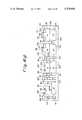
- FIGS. 1(a) to (e)are cross sectional views showing a process of fabricating a Bi-CMOS integrated circuit according to an embodiment of the present invention
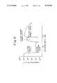
- FIG. 2is a view showing relationship between a concentration and a depth of diffusion in a V-PNP bipolar transistor fabricated by the process of the present invention
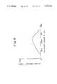
- FIG. 3is a graph showing the relationship between cut-off frequency (f T ) and current in the collector (Ic) in the V-PNP bipolar transistor fabricated by the process of the present invention
- FIG. 4(a) to (e)are cross sectional views showing a related process for fabricating a Bi-CMOS integrated circuit
- FIGS. 4(f) and (g)are cross sectional views showing a further related process for fabricating another Bi-CMOS integrated circuit
- FIG. 5is a graph showing the relationship between the concentration and depth of diffusion in a V-PNP bipolar transistor fabricated by the related process.
- FIG. 6is a view showing the relationship between cut-off frequency (f T ) and current in the collector (Ic) in the V-PNP bipolar transistor fabricated by the related process.
- an NPN bipolar transistor forming region 101 of a P-type silicon substrate (hereinafter referred to as substrate) 100a N-type first buried layer 105 having a sheet resistance of 50 ⁇ / ⁇ using a known photolithography and ion implantation and an annealing technique.
- a V-PNP bipolar transistor forming region 102 of the substrate 100there is formed on a V-PNP bipolar transistor forming region 102 of the substrate 100 the N-type first buried layer 105 and a P-type second buried layer 106 inside the N-type first buried layer 105 isolated by the N-type first buried layer 105 from the substrate 100 and having a sheet resistance 350 ⁇ using a known photolithography and ion implantation and an annealing technique.
- the N-type first buried layer 105is also formed on a P-channel MOS transistor forming region 103 and the second buried layer 106 is formed on an N-channel MOS transistor forming region 104 using a known photolithography and ion implantation and an annealing technique.
- a P-type epitaxial film 10 having the impurity concentration of 1.5 ⁇ 10 15 atoms/cm 3is deposited and grown int he thickness of 2 to 4 ⁇ m on the surface of the substrate 100 using an epitaxial technique. Then, as shown in FIG. 1(b), a P-type epitaxial film 10 having the impurity concentration of 1.5 ⁇ 10 15 atoms/cm 3 is deposited and grown int he thickness of 2 to 4 ⁇ m on the surface of the substrate 100 using an epitaxial technique. Then, as shown in FIG.
- an N-type diffused 11for forming a P-channel MOS transistor, for forming an NPN bipolar transistor and for forming the V-PNP bipolar transistor, all of which are greater than the N-type first buried layer 105 of the V-PNP bipolar transistor forming region 102 in the sizes thereof and have a surface concentration of 5 ⁇ 10 16 atoms/cm 3 with a diffusion depth of 1 to 2 ⁇ m. Accordingly, the N-regions 11, 12 and 13 are connected to the first buried layers 14 previously buried in the substrate 100.
- the first buried layer 14 connected to the N-region 11 for forming the P-channel MOS transistor and the first buried layer 14 connected to the N-region 12 for forming the NPN bipolar transistorcorrespond respectively to the first buried layer 105, while the first buried layer 14 connected to the N-region 13 of the V-PNP bipolar transistor correspond to the first and second buried layers 105 and 106.
- the second buried layer 106is diffused upward into the epitaxial film 10 more than the first buried layer 105 at the V-PNP bipolar transistor region 102.
- a P-type buried layer 112 functioning as a collector of the V-PNP bipolar transistor isolated from the substrate 100is formed on the first buried layer 14
- LOCOS oxide films 113on the substrate formed in the processes set for the above as shown in FIG. 1(d), and the LOCOS oxide films 113 have thickness of 7000 angstroms. Thereafter, a layer 114 for forming the collector contact of the NPN-bipolar transistor is formed by diffusion of the N-type impurity.
- a P-type diffusion layer 115 for forming the collector contact of the V-PNP bipolar transistoris formed inside the N-region 13 for forming the V-PNP bipolar transistor to reach the P-type buried layer 112 by diffusion a P-type impurity.
- a P-type diffusion layer 116as a base of the NPN bipolar transistor, have the surface concentration of 5 ⁇ 10 17 atoms/cm 3 with a diffusion depth of 0.6 ⁇ m.
- a gate oxide film 117 and a polysilicon gate 118on the semiconductor substrate as shown in FIG. 1(e) using the known MOS gate forming technique and in a manner similar to that of FIG. 4(e).
- N-type diffusion layers as an emitter 119 of the NPN bipolar transistor, as a base contact 120 of the V-PNP bipolar transistor as a source/drain 121 of the N-channel MOS transistorare formed using an arsenic implantation technique, and P-type diffused layers as a base contact 122 of the NPN bipolar transistor as an emitter 123 of the V-PNP bipolar transistor and as a source/drain 124 of the P-channel MOS transistor are formed using a BF 2 ion implantation technique.
- the process of the Bi-CMOS integrated circuitis accomplished after opening contact holes for wiring each of the elements and applying aluminum electrodes using the known technique.
- the P-type epitaxial film 10is formed after formation of the first buried layer 105 and the second buried layer 106 according to the first embodiment, it is possible to sufficiently control the occurrence of the auto-doping phenomenon which occurs when boron is doped in the epitaxial film in the fabrication of the Bi-CMOS including a V-PNP bipolar transistor. Furthermore, since the N-type diffusion layer 13 as a base can be formed on the V-PNP bipolar transistor forming region 102, it is possible to provide the impurity concentration gradient in the layer 13 for forming the N-type base for the electric field aiding effect.
- the N-regions of the active regionshave the N-type diffusion which results in elimination of formation of the P-type buried layer in the isolation region.
- the auto-doping phenomenonhas less occurred when the epitaxial film is formed.
Landscapes
- Metal-Oxide And Bipolar Metal-Oxide Semiconductor Integrated Circuits (AREA)
- Bipolar Transistors (AREA)
Abstract
Description
This application claims the right of priority under 35 U.S.C. 119 of Japanese Patent Application Serial No. 11034/1990 filed on Apr. 27, 1990, the entire disclosure of which is incorporated herein by reference.
1. Field of the Invention
The present invention relates to a Bi-CMOS integrated circuit including a vertical type PNP bipolar transistor capable of operating at high speed.
2. Description of the Related Art
Conventionally, in Bi-CMOS integrated circuits, bipolar devices and CMOS devices have been formed on the same chip so that the driving capability of the CMOS devices are enhanced by the bipolar devices in order to obtain a high responsive CMOS. Although the Bi-CMOS integrated circuits have exhibited both bipolar and CMOS characteristics, they have not been able to give excellent functions such as high speed operation, high integration, high driving capability, low power consumption and the like.
A process of fabricating Bi-CMOS integrated circuits will be described hereinafter with reference to FIGS. 4(a) to (e).
As shown in FIG. 4(a), a first N-type buriedlayer 105 having a sheet resistance of 50 Ω/□ is formed on an NPN bipolartransistor forming region 101 of a P-type silicon substrate (hereinafter referred to as substrate) 100.
Also formed on a vertical type PNP (hereinafter referred to as V-PNP) bipolartransistor forming region 102 are the N-type first buriedlayer 105 and a P-type second buriedlayer 106 having a sheet resistance of 350 Ω/□ which is isolated from thesubstrate 100 by the N-type first buriedlayer 105.
The N-type first buriedlayer 105 is also formed on a P-channel MOStransistor forming region 103 and the P-type second buriedlayer 106 is also formed on an N-channel MOStransistor forming region 104. Thefirst isolation layers 107 are formed on thesubstrate 100 for isolating an element in the NPN bipolartransistor forming region 101 and an element in the V-PNP bipolartransistor forming region 102 respectively at the same time that the P-type second buriedlayer 106 is formed using a known photolithography technique and an ion implantation and an annealing technique.
Subsequently, as shown in FIG. 4(b), an N-typeepitaxial film 108 having the N-type impurity concentration of 1.5×10¹⁶ atoms/cm3 is deposited and grown in the thickness of 2 to 4 μm on the surface of thesubstrate 100 using an epitaxial technique. Then, as shown in FIG. 4(c), there are formed on the N-type epitaxial film 108 asecond isolation layer 109 for isolating elements and a P-type region (hereinafter referred to as P-region) 110 for forming an N-channel MOS transistor thereon respectively having surface concentration of 2E16 atoms/cm3 and diffusion depth of 1-2 μm so that the previously buriedfirst isolation layers 107 andsecond isolation layers 109 are connected with each other, and the P-region 110 and the P-type region 111, formed by the out diffusion of second buriedlayer 106 in thedevice forming region 104 are connected with each other.
Whereupon, inasmuch as thefirst isolation layers 107 are formed of antimony and thesecond isolation layers 109 are formed of boron, the second P-type buriedlayer 106 is diffused more deeply upward in the N-typeepitaxial film 108 than the N-type first buriedlayer 105 at the V-PNP bipolartransistor forming region 102. As a result, over the first N-type buriedlayer 105 there is formed a P-type buriedlayer 112 serving as a collector of the V-PNPbipolar transistor 102 isolated from thesubstrate 100.
Thereafter, LOCOSoxide films 113 are formed due to isolation of MOS device in the thickness of about 7000 angstroms by the LOCOS (localized oxidation of silicon) method on the substrate as shown in FIG. 4(d) which has therein thesecond isolation layers 109, the P-region 110 and the second buriedlayer 111.
Then, alayer 114 forming a collector contact of the NPN bipolar transistor is formed by diffusion of the N-type impurity. Successibly, alayer 115 for forming a collector contact of the V-PNP transistor is formed by diffusion of the P-type impurity to reach the P-type buriedlayer 112.
Then, a P-type layer 116 for forming a base of the NPN transmitter is formed with a surface concentration of 5E17 atoms/cm3, and in a diffusion depth of 0.6 μm.
As shown in FIG. 4(e), on the substrate set forth above agate oxide film 117 and apolysilicon gate 118, using a known MOS gate forming technique, are formed for the MOS transistors.
Then, there are formed alayer 119 for forming an emitter of the NPN bipolar transistor and alayer 120 for forming a base contact of the V-PNP transistor and alayer 121 for forming a source and a drain (hereinafter referred to as source/drain) of the N-channel MOS transistor using an arsenic implantation technique.
There are formed alayer 122 for forming a base contact of the NPN bipolar transistor, alayer 123 for forming an emitter of the V-PNP bipolar transistor and alayer 124 for forming a source/drain of the P-channel MOS transistor using a BF2 ion implantation technique.
Thereafter, the Bi-CMOS structure is completed by opening contact holes for wiring each of the elements and applying aluminum electrodes using a known technique whose detailed description is omitted.
The Bi-CMOS integrated circuit fabricated in the process set forth above has a concentration characteristics as illustrated in FIG. 5 and a high-frequency characteristics as illustrated in FIG. 6. That is, inasmuch as the V-PNP bipolar transistor has a base layer formed by the N-type epitaxial film having a uniform concentration as shown in FIG. 5, the high-frequency characteristics thereof, i.e., a cut-off frequency fT becomes about 200 MHz, which results in reducing the operation speed at one tenth or less of the other Bi-CMOSs.
Since the base region in the PNP bipolar transistor is formed of the epitaxial layer having a uniform concentration, the minority carriers injected from the emitter region to the base region are not subjected to an electric field aiding effect.
Accordingly, there was a problem that the Bi-CMOS integrated circuit is deteriorated in its fT -IC characteristic compared with the PNP bipolar transistor having a diffused base which is known by the following equation.
1/2πf.sub.T =τe+τb+τx+τc (1)
where a second term τb (base time constant) is largest and is expressed as:
τb=W.sub.B.sup.2 /nD.sub.B ( 2)
where WB is a base width, n is a constant dependent on minority carrier distribution in the base and DB is a diffusion constant of the minority carrier concentration in the base.
The epitaxial PNP bipolar transistor is a transistor having normally a uniform base so that it is not influenced by the electric field aiding effect caused by a diffusion gradient. As a result, the base time constant of the epitaxial PNP bipolar transistor τb is greater than but the cut-off frequency fT thereof is less than those of the transistor having the diffused base.
Another fabrication process has been proposed to solve the problem set forth above.
Firstly, in FIG. 4(f) over the surface of thesubstrate 100 as illustrated in FIG. 4(a), the N-typeepitaxial film 108 having an N-type impurity concentration of 1.5E 15 atoms/cm3 is formed in the depth of 2 to 4 μm. Secondly,second isolation layers 109 for isolating each element and a P-region 110 for forming the N-channel MOS transistor are formed at the same time with the surface concentration of 2×10¹⁶ atoms/cm3 in the depth of 1 to 2 μm, then thefirst isolation layers 107 are connected to thesecond isolation layers 109 and the second buriedlayer 111 is connected to the P-region 110. By such an arrangement, over the first buriedlayer 105 at the V-PNP bipolartransistor forming region 102 there is formed the P-type buriedlayer 112 serving as the collector of the V-PNP bipolar transistor.
Thereafter, an N-type diffusion region (hereinafter referred to as N-region) 125 for forming the P-channel MOS transistor is formed and the same N-region 125 having the surface concentration 5×10¹⁶ atoms/cm3 with the diffusion depth of 1 to 2 μm is formed at the V-PNP transistor bipolartransistor forming region 102 to reach the P-type buriedlayer 112.
Then, there are formed, as shown in FIG. 4(g), theLOCOS oxide film 112, the N-type layer 114 for forming the collector contact of the NPN bipolar transistor and thebase layer 116 of the NPN bipolar transistor in the same manner as in FIG. 4(d).
Thereafter, in the same way as in FIG. 4(e), there are formed respectively thegate oxide film 117, thepolysilicon gate 118, theemitter layer 119 of the NPN bipolar transistor, thelayer 120 for forming the base contact of the V-PNP bipolar transistor, the source/drain 121 of the N-channel MOS transistor, thelayer 122 for forming the base contact of the NPN bipolar transistor,emitter layer 123 of the V-PNP bipolar transistor and the source/drain 124 of the P-channel MOS transistor.
According to the process set forth above, the V-PNP bipolar transistor can be formed in the N-region which is formed by the diffusion technique so that the cut-off frequency fT is improved. However, the N-type epitaxial film should have the low concentration, i.e. the N-type impurity concentration of 1.5×10¹⁵ atoms/cm3 to form the due to the MOS characteristics and the concentration of the N-region should be sufficiently lower than the same value in view of the process margin.
However, in the case of the Bi-CMOS integrated circuit including the V-PNP bipolar transistor, the surface concentration of the P-type second buriedlayer 111 formed of boron should be high and the area thereof should be large in view of the wafer so that an auto-doping phenomenon occurs in the wafer per se when the wafer epitaxial film is formed. Therefore, it was difficult to control the N-type specific resistivity of the epitaxial film to the low concentration.
Accordingly, when the control characteristics of the concentration of the N-type epitaxial film is improved in the conventional fabrication process, the high frequency characteristics are determined because the concentration of the base of the bipolar transistor becomes uniform, while when the high frequency characteristics are improved, the high frequency characteristics is deteriorated so that the control of the N-type epitaxial film becomes difficult. The relationship between the control of the concentration and the high frequency characteristics is a so-called tradeoff, and hence, quick improvement thereof has been demanded.
It is an object of the present invention to provide a process for fabricating a Bi-CMOS integrated circuit capable of improving the control characteristics of the concentration of an epitaxial film and also improving the high frequency characteristics.
To achieve the above object, the present process comprising the steps of forming an epitaxial film on the substrate, the epitaxial film having the surface concentration which is lower than that of a P-channel portion of a P-channel MOS transistor, forming a PNP bipolar transistor forming region and a P-channel MOS transistor forming region respectively formed on the epitaxial film, both the PNP bipolar transistor forming region and the P-channel MOS transistor forming region having N-type buried layers, forming N-regions by diffusing N-type buried layers, forming N-regions by diffusing N-type impurities having concentration higher than that of P-type impurity in the epitaxial film and connected to the N-type buried layers and forming an PNP bipolar transistor and a P-channel MOS transistor on the N-regions.
According to the present invention, inasmuch as the epitaxial film is formed of a P-type material having low concentration, i.e. the concentration lower than that of the surface concentration of the P-channel portion of the N-channel MOS transistor, it is possible to control an auto-doping phenomenon at the low concentration which occurs when boron is doped in the epitaxial film in the fabrication of the Bi-CMOS including V-PNP bipolar transistor.
Furthermore, according to the present invention, inasmuch as there is formed the P-type epitaxial film having low concentration, it is possible to form a diffusion layer on the PNP bipolar transistor forming region. Accordingly, it is possible to form the N-type base layer of the bipolar transistor having an impurity concentration gradient for the electric field aiding effect which entails the improvement of the high frequency characteristics of the bipolar transistor.
Still, furthermore, according to the present invention, inasmuch as the P-type epitaxial film having low concentration is formed, it is possible to form a diffusion layer in the epitaxial film while the diffusion layer has a concentration of 5×10¹⁶ atoms/cm2 determined by the MOS characteristics in the MOS transistor forming region.
These and other features and advantages of the invention may be more completely understood from the following detailed description of the preferred embodiment of the invention with reference to the accompanying drawings in which:
FIGS. 1(a) to (e) are cross sectional views showing a process of fabricating a Bi-CMOS integrated circuit according to an embodiment of the present invention;
FIG. 2 is a view showing relationship between a concentration and a depth of diffusion in a V-PNP bipolar transistor fabricated by the process of the present invention;
FIG. 3 is a graph showing the relationship between cut-off frequency (fT) and current in the collector (Ic) in the V-PNP bipolar transistor fabricated by the process of the present invention;
FIG. 4(a) to (e) are cross sectional views showing a related process for fabricating a Bi-CMOS integrated circuit;
FIGS. 4(f) and (g) are cross sectional views showing a further related process for fabricating another Bi-CMOS integrated circuit;
FIG. 5 is a graph showing the relationship between the concentration and depth of diffusion in a V-PNP bipolar transistor fabricated by the related process; and
FIG. 6 is a view showing the relationship between cut-off frequency (fT) and current in the collector (Ic) in the V-PNP bipolar transistor fabricated by the related process.
Explanation will be made of a process of fabricating a Bi-CMOS integrated circuit according to the present invention with reference to the drawing in which like reference characters are used to designate like or corresponding part throughout the drawings which schematically illustrates these parts for the sake of understanding.
Accordingly, dimensions, shapes and arrangements which will be explained in the following preferred embodiment are only of illustrative purposes and are not of restrictive purposes, and therefore, the conception or technical scope of the present invention should not be limited to these preferred embodiment.
As shown in FIG. 1(a), there is formed on an NPN bipolartransistor forming region 101 of a P-type silicon substrate (hereinafter referred to as substrate) 100 a N-type first buriedlayer 105 having a sheet resistance of 50 Ω/□ using a known photolithography and ion implantation and an annealing technique.
There is formed on a V-PNP bipolartransistor forming region 102 of thesubstrate 100 the N-type first buriedlayer 105 and a P-type second buriedlayer 106 inside the N-type first buriedlayer 105 isolated by the N-type first buriedlayer 105 from thesubstrate 100 and having a sheet resistance 350 Ω□ using a known photolithography and ion implantation and an annealing technique.
Furthermore, the N-type first buriedlayer 105 is also formed on a P-channel MOStransistor forming region 103 and the second buriedlayer 106 is formed on an N-channel MOStransistor forming region 104 using a known photolithography and ion implantation and an annealing technique.
Subsequently, as shown in FIG. 1(b), a P-type epitaxial film 10 having the impurity concentration of 1.5×10¹⁵ atoms/cm3 is deposited and grown int he thickness of 2 to 4 μm on the surface of thesubstrate 100 using an epitaxial technique. Then, as shown in FIG. 1(c), there are formed an N-type diffused 11 for forming a P-channel MOS transistor, for forming an NPN bipolar transistor and for forming the V-PNP bipolar transistor, all of which are greater than the N-type first buriedlayer 105 of the V-PNP bipolartransistor forming region 102 in the sizes thereof and have a surface concentration of 5×10¹⁶ atoms/cm3 with a diffusion depth of 1 to 2 μm. Accordingly, the N-regions layers 14 previously buried in thesubstrate 100.
The first buriedlayer 14 connected to the N-region 11 for forming the P-channel MOS transistor and the first buriedlayer 14 connected to the N-region 12 for forming the NPN bipolar transistor correspond respectively to the first buriedlayer 105, while the first buriedlayer 14 connected to the N-region 13 of the V-PNP bipolar transistor correspond to the first and second buriedlayers
Inasmuch as each of the N-regions layers 14 and the first buriedlayer 105 is formed of antimony and the second buriedlayer 106 is formed of boron, the second buriedlayer 106 is diffused upward into theepitaxial film 10 more than the first buriedlayer 105 at the V-PNPbipolar transistor region 102.
Accompanied by the diffusion of the second buriedlayer 106, a P-type buriedlayer 112 functioning as a collector of the V-PNP bipolar transistor isolated from thesubstrate 100 is formed on the first buriedlayer 14
Successively, there are formedLOCOS oxide films 113 on the substrate formed in the processes set for the above as shown in FIG. 1(d), and theLOCOS oxide films 113 have thickness of 7000 angstroms. Thereafter, alayer 114 for forming the collector contact of the NPN-bipolar transistor is formed by diffusion of the N-type impurity.
A P-type diffusion layer 115 for forming the collector contact of the V-PNP bipolar transistor is formed inside the N-region 13 for forming the V-PNP bipolar transistor to reach the P-type buriedlayer 112 by diffusion a P-type impurity.
Thereafter, there is formed a P-type diffusion layer 116 as a base of the NPN bipolar transistor, have the surface concentration of 5×10¹⁷ atoms/cm3 with a diffusion depth of 0.6 μm. Then, there are formed agate oxide film 117 and apolysilicon gate 118 on the semiconductor substrate as shown in FIG. 1(e) using the known MOS gate forming technique and in a manner similar to that of FIG. 4(e).
Successively, as shown in FIG. 1(e), N-type diffusion layers as anemitter 119 of the NPN bipolar transistor, as abase contact 120 of the V-PNP bipolar transistor as a source/drain 121 of the N-channel MOS transistor are formed using an arsenic implantation technique, and P-type diffused layers as abase contact 122 of the NPN bipolar transistor as anemitter 123 of the V-PNP bipolar transistor and as a source/drain 124 of the P-channel MOS transistor are formed using a BF2 ion implantation technique. thereafter, the process of the Bi-CMOS integrated circuit is accomplished after opening contact holes for wiring each of the elements and applying aluminum electrodes using the known technique.
Inasmuch as the P-type epitaxial film 10 is formed after formation of the first buriedlayer 105 and the second buriedlayer 106 according to the first embodiment, it is possible to sufficiently control the occurrence of the auto-doping phenomenon which occurs when boron is doped in the epitaxial film in the fabrication of the Bi-CMOS including a V-PNP bipolar transistor. Furthermore, since the N-type diffusion layer 13 as a base can be formed on the V-PNP bipolartransistor forming region 102, it is possible to provide the impurity concentration gradient in thelayer 13 for forming the N-type base for the electric field aiding effect.
Accordingly, the cut-off frequency fT -Ic characteristics of the V-PNP bipolar transistor which shown that the high frequency characteristics can be improved.
Still furthermore, when the elements are isolated, the N-regions of the active regions have the N-type diffusion which results in elimination of formation of the P-type buried layer in the isolation region. As a result, the auto-doping phenomenon has less occurred when the epitaxial film is formed.
Claims (8)
1. A process for fabricating a Bi-CMOS integrated circuit comprising the steps of:
(a) forming simultaneously on a P-type semiconductor substrate N-type buried layers in a P-channel MOS transistor forming region, a PNP transistor forming region and an NPN transistor forming region;
(b) forming simultaneously on the semiconductor substrate a collector forming P-type region having the size smaller than the associated respective N-type buried layer in the PNP transistor forming region, and a P-type buried layer in an N-channel MOS transistor forming region;
(c) forming on the semiconductor substrate a P-type epitaxial film having a first surface concentration;
(d) forming diffused N-type regions, each having a size larger than that of the associated respective N-type buried layer and a second surface concentration greater than said first surface concentration, in the P-type epitaxial film in the PNP transistor forming region, the NPN transistor forming region and the P-channel MOS transistor forming region, with the diffused N-type regions being connected with the respective N-type buried layers in the NPN transistor and P-channel MOS transistor forming regions and with the collector forming P-type region in the PNP transistor forming region;
(e) forming an NPN transistor in the NPN transistor forming region, a vertical PNP transistor in the PNP transistor forming region, with the respective diffused N-type region being the base of the PNP transistor, and a P-channel MOS transistor in the P-channel MOS transistor forming region, whereby the concentration of a channel portion of the P-channel MOS transistor is higher than said first surface concentration and
(f) forming an N-channel MOS transistor in the N-channel MOS transistor forming region.
2. A process for fabricating a Bi-CMOS integrated circuit comprising the steps of:
(a) preparing a semiconductor substrate having thereon an NPN transistor forming region, a PNP transistor forming region, a P-channel MOS transistor forming region and an N-channel MOS transistor forming region;
(b) forming N-type first buried layers simultaneously on the NPN transistor forming region, the PNP transistor forming region and the P-channel MOS transistor region;
(c) forming P-type second buried layers simultaneously on the PNP transistor forming region as a collector of the PNP transistor and on the N-channel MOS transistor forming region after formation of the N-type first buried layers;
(d) forming on the semiconductor substrate a P-type epitaxial film having a surface concentration lower than that of a channel portion of a P-channel MOS transistor; and
(e) forming N-type diffusion layers on the NPN transistor region as a collector of the NPN transistor, on the PNP transistor forming region as a base of the PNP transistor and on the P-channel MOS transistor forming region as a channel forming region of a P-channel MOS transistor, whereby a vertical PNP transistor can be formed in the PNP transistor forming region.
3. A process for fabricating a Bi-CMOS integrated circuit according to claim 2, further comprising the steps of forming a vertical type PNP bipolar transistor in the PNP transistor forming region, and spaced P-type source and drain regions in the N-type diffusion layer in the P-channel MOS transistor forming region.
4. A process for fabricating a Bi-CMOS integrated circuit according to claim 1, wherein said step of forming a vertical PNP transistor further comprises:
(a) forming a collector contact region within the N-type diffused region of the PNP transistor forming region to reach the collector of the PNP transistor;
(b) forming a base contact region on the surface of the N-type diffused region of the PNP transistor forming region; and
(c) forming an emitter region on the surface of the N-type diffused region of the PNP transistor forming region.
5. A process of fabricating a Bi-CMOS integrated circuit according to claim 1, further comprising the step of forming isolation means between the respective transistor forming regions for causing each of the transistors to be electrically isolated.
6. A process for fabricating a Bi-CMOS integrated circuit according to claim 1 wherein said predetermined surface concentration of said epitaxial film is approximately 1.5×10¹⁵ atoms/cm3.
7. A process for fabricating a Bi-CMOS integrated circuit comprising the steps of:
(a) preparing a P-type semiconductor substrate having thereon an NPN transistor forming region, a PNP transistor forming region, a P-channel MOS transistor forming region and an N-channel MOS transistor forming region;
(b) simultaneously forming respective N-type first buried layers on the NPN transistor forming region, the PNP transistor forming region and the P-channel MOS transistor region;
(c) simultaneously forming respective P-type second buried layers on the N-type first buried layer in the PNP transistor forming region as a collector of the PNP transistor, and on the N-channel MOS transistor forming region;
(d) forming on the P-type semiconductor substrate a P-type epitaxial film having a first surface concentration lower than that of a channel portion of a P-channel MOS transistor;
(e) forming respective N-type first diffusion layers in said epitaxial film in the NPN transistor region as a collector of the NPN transistor, in the PNP transistor forming region as a base of the PNP transistor and in the P-channel MOS transistor forming region, with said N-type first diffusion layers reaching the respective buried layers in said transistor forming regions and having a surface concentration greater than said surface concentration;
(f) forming a P-type second diffusion layer, as a base of an NPN transistor, in the first diffusion layer in the NPN transistor forming region;
(g) forming a P-type third diffusion layer, as a collector contact, in the first diffusion layer in the PNP transistor forming region;
(h) forming respective P-type fourth diffusion layers on the surface of the second diffusion layer as a base contact for the NPN transistor, on the surface of the first diffusion layer in the PNP transistor forming region as a emitter to form a vertical PNP transistor, and on the surface of the first diffusion layer in the P-channel MOS transistor forming region as source/drain; and
(i) forming respective N-type fifth diffusion layer on the surface of the second diffusion layer as an emitter of the NPN transistor, on the surface of the first diffusion layer in the PNP transistor forming region as a base contact, and on the surface of the P-type epitaxial film as the source/drain.
8. A process for fabricating a Bi-CMOS integrated circuit as defined in claim 7 wherein said epitaxial layer has a surface concentration of approximately 1.5×10¹⁵ atoms/cm3 and said N-type first diffusion layers have a surface concentration of approximately 5×10¹⁶ atoms/cm3.
Applications Claiming Priority (2)
| Application Number | Priority Date | Filing Date | Title |
|---|---|---|---|
| JP2-110314 | 1990-04-27 | ||
| JP2110314AJP2950577B2 (en) | 1990-04-27 | 1990-04-27 | Method for manufacturing BiCMOS semiconductor integrated circuit |
Publications (1)
| Publication Number | Publication Date |
|---|---|
| US5179036Atrue US5179036A (en) | 1993-01-12 |
Family
ID=14532576
Family Applications (1)
| Application Number | Title | Priority Date | Filing Date |
|---|---|---|---|
| US07/686,429Expired - LifetimeUS5179036A (en) | 1990-04-27 | 1991-04-17 | Process for fabricating Bi-CMOS integrated circuit |
Country Status (2)
| Country | Link |
|---|---|
| US (1) | US5179036A (en) |
| JP (1) | JP2950577B2 (en) |
Cited By (19)
| Publication number | Priority date | Publication date | Assignee | Title |
|---|---|---|---|---|
| US5319234A (en)* | 1992-02-17 | 1994-06-07 | Mitsubishi Denki Kabushiki Kaisha | C-BiCMOS semiconductor device |
| US5387552A (en)* | 1991-03-22 | 1995-02-07 | National Semiconductor Corporation | Method of fabrication of PNP structure in a common substrate containing NPN or MOS structures |
| US5455189A (en)* | 1994-02-28 | 1995-10-03 | National Semiconductor Corporation | Method of forming BICMOS structures |
| US5691226A (en)* | 1995-06-30 | 1997-11-25 | Motorola, Inc. | Method of manufacturing BICMOS integrated circuits |
| US5767551A (en)* | 1995-06-02 | 1998-06-16 | Texas Instruments Incorporated | Intergrated circuit combining high frequency bipolar and high power CMOS transistors |
| US5793085A (en)* | 1993-02-26 | 1998-08-11 | Sgs-Thomson Microelectronics S.R.L. | Bipolar transistor compatible with CMOS processes |
| US5847440A (en)* | 1994-10-13 | 1998-12-08 | Mitsubishi Denki Kabushiki Kaisha | Bipolar transistor, semiconductor device having bipolar transistors |
| US5889315A (en)* | 1994-08-18 | 1999-03-30 | National Semiconductor Corporation | Semiconductor structure having two levels of buried regions |
| US5911104A (en)* | 1998-02-20 | 1999-06-08 | Texas Instruments Incorporated | Integrated circuit combining high frequency bipolar and high power CMOS transistors |
| US6057184A (en)* | 1997-03-21 | 2000-05-02 | International Business Machines Corporation | Semiconductor device fabrication method using connecting implants |
| US6162695A (en)* | 1999-08-18 | 2000-12-19 | Taiwan Semiconductor Manufacturing Company | Field ring to improve the breakdown voltage for a high voltage bipolar device |
| US6249030B1 (en) | 1992-12-07 | 2001-06-19 | Hyundai Electronics Industries Co., Ltd. | BI-CMOS integrated circuit |
| US6759303B1 (en)* | 2000-03-02 | 2004-07-06 | The United States Of America As Represented By The Secretary Of The Navy | Complementary vertical bipolar junction transistors fabricated of silicon-on-sapphire utilizing wide base PNP transistors |
| US6768183B2 (en)* | 2001-04-20 | 2004-07-27 | Denso Corporation | Semiconductor device having bipolar transistors |
| US6794730B2 (en)* | 2000-12-31 | 2004-09-21 | Texas Instruments Incorporated | High performance PNP bipolar device fully compatible with CMOS process |
| US6809024B1 (en) | 2003-05-09 | 2004-10-26 | International Business Machines Corporation | Method to fabricate high-performance NPN transistors in a BiCMOS process |
| US6972466B1 (en)* | 2004-02-23 | 2005-12-06 | Altera Corporation | Bipolar transistors with low base resistance for CMOS integrated circuits |
| US20110198689A1 (en)* | 2010-02-17 | 2011-08-18 | Suku Kim | Semiconductor devices containing trench mosfets with superjunctions |
| US20160240660A1 (en)* | 2015-02-15 | 2016-08-18 | Shanghai Huahong Grace Semiconductor Manufacturing Corporation | High Voltage LDMOS Device with an Increased Voltage at Source (High Side) and a Fabricating Method Thereof |
Citations (6)
| Publication number | Priority date | Publication date | Assignee | Title |
|---|---|---|---|---|
| US4637125A (en)* | 1983-09-22 | 1987-01-20 | Kabushiki Kaisha Toshiba | Method for making a semiconductor integrated device including bipolar transistor and CMOS transistor |
| JPS6443453A (en)* | 1987-08-07 | 1989-02-15 | Canon Kk | Sheet material output device |
| JPS6450349A (en)* | 1987-08-21 | 1989-02-27 | Hitachi Ltd | Superconductive lens for charged particle beam |
| JPH0237765A (en)* | 1988-07-27 | 1990-02-07 | Nec Corp | Manufacture of integrated circuit |
| US4956305A (en)* | 1986-05-30 | 1990-09-11 | Telefunken Electronic Gmbh | Process for fabricating an integrated circuit |
| US4965220A (en)* | 1983-10-07 | 1990-10-23 | Kabushiki Kaisha Toshiba | Method of manufacturing a semiconductor integrated circuit device comprising an MOS transistor and a bipolar transistor |
- 1990
- 1990-04-27JPJP2110314Apatent/JP2950577B2/ennot_activeExpired - Fee Related
- 1991
- 1991-04-17USUS07/686,429patent/US5179036A/ennot_activeExpired - Lifetime
Patent Citations (7)
| Publication number | Priority date | Publication date | Assignee | Title |
|---|---|---|---|---|
| US4637125A (en)* | 1983-09-22 | 1987-01-20 | Kabushiki Kaisha Toshiba | Method for making a semiconductor integrated device including bipolar transistor and CMOS transistor |
| US4694562A (en)* | 1983-09-22 | 1987-09-22 | Kabushiki Kaisha Toshiba | Method for manufacturing a semiconductor integrated device including bipolar and CMOS transistors |
| US4965220A (en)* | 1983-10-07 | 1990-10-23 | Kabushiki Kaisha Toshiba | Method of manufacturing a semiconductor integrated circuit device comprising an MOS transistor and a bipolar transistor |
| US4956305A (en)* | 1986-05-30 | 1990-09-11 | Telefunken Electronic Gmbh | Process for fabricating an integrated circuit |
| JPS6443453A (en)* | 1987-08-07 | 1989-02-15 | Canon Kk | Sheet material output device |
| JPS6450349A (en)* | 1987-08-21 | 1989-02-27 | Hitachi Ltd | Superconductive lens for charged particle beam |
| JPH0237765A (en)* | 1988-07-27 | 1990-02-07 | Nec Corp | Manufacture of integrated circuit |
Cited By (29)
| Publication number | Priority date | Publication date | Assignee | Title |
|---|---|---|---|---|
| US5387552A (en)* | 1991-03-22 | 1995-02-07 | National Semiconductor Corporation | Method of fabrication of PNP structure in a common substrate containing NPN or MOS structures |
| US5319234A (en)* | 1992-02-17 | 1994-06-07 | Mitsubishi Denki Kabushiki Kaisha | C-BiCMOS semiconductor device |
| US20030203559A1 (en)* | 1992-12-07 | 2003-10-30 | Lee Steven S. | BI-CMOS integrated circuit |
| US6249030B1 (en) | 1992-12-07 | 2001-06-19 | Hyundai Electronics Industries Co., Ltd. | BI-CMOS integrated circuit |
| US6943413B2 (en) | 1992-12-07 | 2005-09-13 | Hynix Semiconductor Inc. | BI-CMOS integrated circuit |
| US6593178B1 (en)* | 1992-12-07 | 2003-07-15 | Hyundai Electronics America | BI-CMOS integrated circuit |
| US5793085A (en)* | 1993-02-26 | 1998-08-11 | Sgs-Thomson Microelectronics S.R.L. | Bipolar transistor compatible with CMOS processes |
| US5580798A (en)* | 1994-02-28 | 1996-12-03 | National Semiconductor Corporation | Method of fabricating bipolar transistor having a guard ring |
| US5455189A (en)* | 1994-02-28 | 1995-10-03 | National Semiconductor Corporation | Method of forming BICMOS structures |
| US5889315A (en)* | 1994-08-18 | 1999-03-30 | National Semiconductor Corporation | Semiconductor structure having two levels of buried regions |
| US5899714A (en)* | 1994-08-18 | 1999-05-04 | National Semiconductor Corporation | Fabrication of semiconductor structure having two levels of buried regions |
| US5847440A (en)* | 1994-10-13 | 1998-12-08 | Mitsubishi Denki Kabushiki Kaisha | Bipolar transistor, semiconductor device having bipolar transistors |
| US5917222A (en)* | 1995-06-02 | 1999-06-29 | Texas Instruments Incorporated | Intergrated circuit combining high frequency bipolar and high power CMOS transistors |
| US5767551A (en)* | 1995-06-02 | 1998-06-16 | Texas Instruments Incorporated | Intergrated circuit combining high frequency bipolar and high power CMOS transistors |
| US5691226A (en)* | 1995-06-30 | 1997-11-25 | Motorola, Inc. | Method of manufacturing BICMOS integrated circuits |
| US6097068A (en)* | 1997-03-21 | 2000-08-01 | International Business Machines Corporation | Semiconductor device fabrication method and apparatus using connecting implants |
| US6057184A (en)* | 1997-03-21 | 2000-05-02 | International Business Machines Corporation | Semiconductor device fabrication method using connecting implants |
| US5911104A (en)* | 1998-02-20 | 1999-06-08 | Texas Instruments Incorporated | Integrated circuit combining high frequency bipolar and high power CMOS transistors |
| US6162695A (en)* | 1999-08-18 | 2000-12-19 | Taiwan Semiconductor Manufacturing Company | Field ring to improve the breakdown voltage for a high voltage bipolar device |
| US6759303B1 (en)* | 2000-03-02 | 2004-07-06 | The United States Of America As Represented By The Secretary Of The Navy | Complementary vertical bipolar junction transistors fabricated of silicon-on-sapphire utilizing wide base PNP transistors |
| US6794730B2 (en)* | 2000-12-31 | 2004-09-21 | Texas Instruments Incorporated | High performance PNP bipolar device fully compatible with CMOS process |
| US6768183B2 (en)* | 2001-04-20 | 2004-07-27 | Denso Corporation | Semiconductor device having bipolar transistors |
| US6809024B1 (en) | 2003-05-09 | 2004-10-26 | International Business Machines Corporation | Method to fabricate high-performance NPN transistors in a BiCMOS process |
| US20040222497A1 (en)* | 2003-05-09 | 2004-11-11 | International Business Machines Corporation | Method to fabricate high-performance npn transistors in a bicmos process |
| US6972466B1 (en)* | 2004-02-23 | 2005-12-06 | Altera Corporation | Bipolar transistors with low base resistance for CMOS integrated circuits |
| US7285454B1 (en) | 2004-02-23 | 2007-10-23 | Altera Corporation | Bipolar transistors with low base resistance for CMOS integrated circuits |
| US20110198689A1 (en)* | 2010-02-17 | 2011-08-18 | Suku Kim | Semiconductor devices containing trench mosfets with superjunctions |
| US20160240660A1 (en)* | 2015-02-15 | 2016-08-18 | Shanghai Huahong Grace Semiconductor Manufacturing Corporation | High Voltage LDMOS Device with an Increased Voltage at Source (High Side) and a Fabricating Method Thereof |
| US9543432B2 (en)* | 2015-02-15 | 2017-01-10 | Shanghai Huahong Grace Semiconductor Manufacturing Corporation | High voltage LDMOS device with an increased voltage at source (high side) and a fabricating method thereof |
Also Published As
| Publication number | Publication date |
|---|---|
| JPH0410562A (en) | 1992-01-14 |
| JP2950577B2 (en) | 1999-09-20 |
Similar Documents
| Publication | Publication Date | Title |
|---|---|---|
| US5179036A (en) | Process for fabricating Bi-CMOS integrated circuit | |
| US5066602A (en) | Method of making semiconductor ic including polar transistors | |
| US4120707A (en) | Process of fabricating junction isolated IGFET and bipolar transistor integrated circuit by diffusion | |
| US4484388A (en) | Method for manufacturing semiconductor Bi-CMOS device | |
| US5856003A (en) | Method for forming pseudo buried layer for sub-micron bipolar or BiCMOS device | |
| US4694562A (en) | Method for manufacturing a semiconductor integrated device including bipolar and CMOS transistors | |
| US3955269A (en) | Fabricating high performance integrated bipolar and complementary field effect transistors | |
| KR930008018B1 (en) | Bicmos device and manufacturing method of the same | |
| US4311532A (en) | Method of making junction isolated bipolar device in unisolated IGFET IC | |
| JPH0315346B2 (en) | ||
| US4662057A (en) | Method of manufacturing a semiconductor integrated circuit device | |
| JP2824263B2 (en) | High voltage merged bipolar / CMOS integrated circuit | |
| US5162252A (en) | Method of fabricating iil and vertical complementary bipolar transistors | |
| US5837590A (en) | Isolated vertical PNP transistor without required buried layer | |
| US5057894A (en) | Semiconductor integrated circuit device | |
| JPH0348458A (en) | Bi-CMOS integrated circuit and its manufacturing method | |
| JP2985824B2 (en) | Semiconductor device and manufacturing method thereof | |
| US6107146A (en) | Method of replacing epitaxial wafers in CMOS process | |
| US5506156A (en) | Method of fabricating bipolar transistor having high speed and MOS transistor having small size | |
| US5258644A (en) | Semiconductor device and method of manufacture thereof | |
| JP3077168B2 (en) | Bi-MOS semiconductor device and method of manufacturing the same | |
| JP2537886B2 (en) | Semiconductor device | |
| JPS6140140B2 (en) | ||
| KR100296707B1 (en) | Bipolar transistor and method for fabricating the same | |
| JPH0580155B2 (en) |
Legal Events
| Date | Code | Title | Description |
|---|---|---|---|
| AS | Assignment | Owner name:OKI ELECTRIC INDUSTRY CO., LTD., 7-12, TORANOMON 1 Free format text:ASSIGNMENT OF ASSIGNORS INTEREST.;ASSIGNOR:MATSUMOTO, RYOICHI;REEL/FRAME:005683/0909 Effective date:19910412 | |
| FEPP | Fee payment procedure | Free format text:PAYOR NUMBER ASSIGNED (ORIGINAL EVENT CODE: ASPN); ENTITY STATUS OF PATENT OWNER: LARGE ENTITY | |
| STCF | Information on status: patent grant | Free format text:PATENTED CASE | |
| FPAY | Fee payment | Year of fee payment:4 | |
| FPAY | Fee payment | Year of fee payment:8 | |
| FPAY | Fee payment | Year of fee payment:12 | |
| AS | Assignment | Owner name:OKI SEMICONDUCTOR CO., LTD., JAPAN Free format text:CHANGE OF NAME;ASSIGNOR:OKI ELECTRIC INDUSTRY CO., LTD.;REEL/FRAME:022240/0984 Effective date:20081001 |