US5178682A - Method for forming a thin layer on a semiconductor substrate and apparatus therefor - Google Patents
Method for forming a thin layer on a semiconductor substrate and apparatus thereforDownload PDFInfo
- Publication number
- US5178682A US5178682AUS07/687,154US68715491AUS5178682AUS 5178682 AUS5178682 AUS 5178682AUS 68715491 AUS68715491 AUS 68715491AUS 5178682 AUS5178682 AUS 5178682A
- Authority
- US
- United States
- Prior art keywords
- compartment
- semiconductor substrate
- substrate
- forming
- oxide
- Prior art date
- Legal status (The legal status is an assumption and is not a legal conclusion. Google has not performed a legal analysis and makes no representation as to the accuracy of the status listed.)
- Expired - Fee Related
Links
Images


Classifications
- H—ELECTRICITY
- H01—ELECTRIC ELEMENTS
- H01L—SEMICONDUCTOR DEVICES NOT COVERED BY CLASS H10
- H01L21/00—Processes or apparatus adapted for the manufacture or treatment of semiconductor or solid state devices or of parts thereof
- H01L21/02—Manufacture or treatment of semiconductor devices or of parts thereof
- H01L21/02041—Cleaning
- H01L21/02043—Cleaning before device manufacture, i.e. Begin-Of-Line process
- H—ELECTRICITY
- H01—ELECTRIC ELEMENTS
- H01L—SEMICONDUCTOR DEVICES NOT COVERED BY CLASS H10
- H01L21/00—Processes or apparatus adapted for the manufacture or treatment of semiconductor or solid state devices or of parts thereof
- H01L21/02—Manufacture or treatment of semiconductor devices or of parts thereof
- H01L21/02104—Forming layers
- H01L21/02107—Forming insulating materials on a substrate
- H01L21/02109—Forming insulating materials on a substrate characterised by the type of layer, e.g. type of material, porous/non-porous, pre-cursors, mixtures or laminates
- H01L21/02112—Forming insulating materials on a substrate characterised by the type of layer, e.g. type of material, porous/non-porous, pre-cursors, mixtures or laminates characterised by the material of the layer
- H01L21/02123—Forming insulating materials on a substrate characterised by the type of layer, e.g. type of material, porous/non-porous, pre-cursors, mixtures or laminates characterised by the material of the layer the material containing silicon
- H01L21/0217—Forming insulating materials on a substrate characterised by the type of layer, e.g. type of material, porous/non-porous, pre-cursors, mixtures or laminates characterised by the material of the layer the material containing silicon the material being a silicon nitride not containing oxygen, e.g. SixNy or SixByNz
- H—ELECTRICITY
- H01—ELECTRIC ELEMENTS
- H01L—SEMICONDUCTOR DEVICES NOT COVERED BY CLASS H10
- H01L21/00—Processes or apparatus adapted for the manufacture or treatment of semiconductor or solid state devices or of parts thereof
- H01L21/02—Manufacture or treatment of semiconductor devices or of parts thereof
- H01L21/02104—Forming layers
- H01L21/02107—Forming insulating materials on a substrate
- H01L21/02225—Forming insulating materials on a substrate characterised by the process for the formation of the insulating layer
- H01L21/0226—Forming insulating materials on a substrate characterised by the process for the formation of the insulating layer formation by a deposition process
- H01L21/02263—Forming insulating materials on a substrate characterised by the process for the formation of the insulating layer formation by a deposition process deposition from the gas or vapour phase
- H01L21/02271—Forming insulating materials on a substrate characterised by the process for the formation of the insulating layer formation by a deposition process deposition from the gas or vapour phase deposition by decomposition or reaction of gaseous or vapour phase compounds, i.e. chemical vapour deposition
- H—ELECTRICITY
- H01—ELECTRIC ELEMENTS
- H01L—SEMICONDUCTOR DEVICES NOT COVERED BY CLASS H10
- H01L21/00—Processes or apparatus adapted for the manufacture or treatment of semiconductor or solid state devices or of parts thereof
- H01L21/02—Manufacture or treatment of semiconductor devices or of parts thereof
- H01L21/02104—Forming layers
- H01L21/02107—Forming insulating materials on a substrate
- H01L21/02296—Forming insulating materials on a substrate characterised by the treatment performed before or after the formation of the layer
- H01L21/02299—Forming insulating materials on a substrate characterised by the treatment performed before or after the formation of the layer pre-treatment
- H01L21/02301—Forming insulating materials on a substrate characterised by the treatment performed before or after the formation of the layer pre-treatment in-situ cleaning
- H—ELECTRICITY
- H01—ELECTRIC ELEMENTS
- H01L—SEMICONDUCTOR DEVICES NOT COVERED BY CLASS H10
- H01L21/00—Processes or apparatus adapted for the manufacture or treatment of semiconductor or solid state devices or of parts thereof
- H01L21/02—Manufacture or treatment of semiconductor devices or of parts thereof
- H01L21/02104—Forming layers
- H01L21/02107—Forming insulating materials on a substrate
- H01L21/02296—Forming insulating materials on a substrate characterised by the treatment performed before or after the formation of the layer
- H01L21/02299—Forming insulating materials on a substrate characterised by the treatment performed before or after the formation of the layer pre-treatment
- H01L21/0231—Forming insulating materials on a substrate characterised by the treatment performed before or after the formation of the layer pre-treatment treatment by exposure to electromagnetic radiation, e.g. UV light
- H—ELECTRICITY
- H01—ELECTRIC ELEMENTS
- H01L—SEMICONDUCTOR DEVICES NOT COVERED BY CLASS H10
- H01L21/00—Processes or apparatus adapted for the manufacture or treatment of semiconductor or solid state devices or of parts thereof
- H01L21/02—Manufacture or treatment of semiconductor devices or of parts thereof
- H01L21/02104—Forming layers
- H01L21/02107—Forming insulating materials on a substrate
- H01L21/02296—Forming insulating materials on a substrate characterised by the treatment performed before or after the formation of the layer
- H01L21/02299—Forming insulating materials on a substrate characterised by the treatment performed before or after the formation of the layer pre-treatment
- H01L21/02312—Forming insulating materials on a substrate characterised by the treatment performed before or after the formation of the layer pre-treatment treatment by exposure to a gas or vapour
- H—ELECTRICITY
- H01—ELECTRIC ELEMENTS
- H01L—SEMICONDUCTOR DEVICES NOT COVERED BY CLASS H10
- H01L21/00—Processes or apparatus adapted for the manufacture or treatment of semiconductor or solid state devices or of parts thereof
- H01L21/02—Manufacture or treatment of semiconductor devices or of parts thereof
- H01L21/02104—Forming layers
- H01L21/02365—Forming inorganic semiconducting materials on a substrate
- H01L21/02367—Substrates
- H01L21/0237—Materials
- H01L21/02373—Group 14 semiconducting materials
- H01L21/02381—Silicon, silicon germanium, germanium
- H—ELECTRICITY
- H01—ELECTRIC ELEMENTS
- H01L—SEMICONDUCTOR DEVICES NOT COVERED BY CLASS H10
- H01L21/00—Processes or apparatus adapted for the manufacture or treatment of semiconductor or solid state devices or of parts thereof
- H01L21/02—Manufacture or treatment of semiconductor devices or of parts thereof
- H01L21/02104—Forming layers
- H01L21/02365—Forming inorganic semiconducting materials on a substrate
- H01L21/02518—Deposited layers
- H01L21/02521—Materials
- H01L21/02524—Group 14 semiconducting materials
- H01L21/02532—Silicon, silicon germanium, germanium
- H—ELECTRICITY
- H01—ELECTRIC ELEMENTS
- H01L—SEMICONDUCTOR DEVICES NOT COVERED BY CLASS H10
- H01L21/00—Processes or apparatus adapted for the manufacture or treatment of semiconductor or solid state devices or of parts thereof
- H01L21/02—Manufacture or treatment of semiconductor devices or of parts thereof
- H01L21/02104—Forming layers
- H01L21/02365—Forming inorganic semiconducting materials on a substrate
- H01L21/02612—Formation types
- H01L21/02617—Deposition types
- H01L21/0262—Reduction or decomposition of gaseous compounds, e.g. CVD
- H—ELECTRICITY
- H01—ELECTRIC ELEMENTS
- H01L—SEMICONDUCTOR DEVICES NOT COVERED BY CLASS H10
- H01L21/00—Processes or apparatus adapted for the manufacture or treatment of semiconductor or solid state devices or of parts thereof
- H01L21/02—Manufacture or treatment of semiconductor devices or of parts thereof
- H01L21/04—Manufacture or treatment of semiconductor devices or of parts thereof the devices having potential barriers, e.g. a PN junction, depletion layer or carrier concentration layer
- H01L21/18—Manufacture or treatment of semiconductor devices or of parts thereof the devices having potential barriers, e.g. a PN junction, depletion layer or carrier concentration layer the devices having semiconductor bodies comprising elements of Group IV of the Periodic Table or AIIIBV compounds with or without impurities, e.g. doping materials
- H01L21/28—Manufacture of electrodes on semiconductor bodies using processes or apparatus not provided for in groups H01L21/20 - H01L21/268
- H01L21/283—Deposition of conductive or insulating materials for electrodes conducting electric current
- H01L21/285—Deposition of conductive or insulating materials for electrodes conducting electric current from a gas or vapour, e.g. condensation
- H01L21/28506—Deposition of conductive or insulating materials for electrodes conducting electric current from a gas or vapour, e.g. condensation of conductive layers
- H01L21/28512—Deposition of conductive or insulating materials for electrodes conducting electric current from a gas or vapour, e.g. condensation of conductive layers on semiconductor bodies comprising elements of Group IV of the Periodic Table
- H01L21/28525—Deposition of conductive or insulating materials for electrodes conducting electric current from a gas or vapour, e.g. condensation of conductive layers on semiconductor bodies comprising elements of Group IV of the Periodic Table the conductive layers comprising semiconducting material
Definitions
- This inventionrelates to a method for forming a thin layer of material on the surface of a semiconductor substrate and an apparatus for the same.
- this inventionrelates to a novel method for forming a thin layer of material on the surface of a semiconductor substrate after the substrate surface ha been cleared of unwanted organic contaminants, metal contaminants and damaged surface, and without exposing the cleaned substrate surface to the ambient air, and an apparatus for carrying out the method.
- Performance characteristics of electronics devicesare readily and adversely affected by contaminants introduced on purpose or by accident in the course of the manufacturing process. In order to avoid any introduction of contaminants into the electronics products as much as possible, it is necessary to keep the whole manufacturing environment at a maximum possible degree of cleanness. In this connection, highly advanced cleaning and purifying technologies are employed to produce desired starting materials and processing environments for the manufacture of the devices.
- the manufacturing process for semiconductor devicesis roughly divided into a thin film formation and a circuit pattern formation.
- the process for forming thin films or layers of material on the semiconductor substrateis further divided into many subprocesses depending on the material of which the thin films are made and techniques to be used to form them.
- Various cleaning technologies for each of the subprocesses or to be shared by some of the subprocesseshave been developed into practical use.
- Important and essential to all these subprocessesis the pretreatment of the semiconductor substrate which is performed prior to forming the thin films on the substrate.
- the semiconductor substrateis cleaned with water, acid or alkalis or it is subjected to chemical oxidation or treatment with diluted hydrofluoric acid solution for the removal of grease heavy metals, naturally grown oxide film and the like.
- solution cleaning techniquesare widely used in the industry but are disadvantageous in that the cleaned semiconductor substrate is unavoidably exposed to the surrounding air before it is coated with thin films in a subsequent process.
- the exposure to the aircauses a thin oxide film to grown on the substrate surface, especially when the substrate contains active semiconductor substance or it has exposed metal portions thereon. For this reason, the substrate cleaning with solutions falls short of complete cleaning of the substrate surface although it is effective to remove heavy metal and organic contaminants.
- the growth of a natural oxide film on the semiconductor substratehas an adverse effect on the quality of various thin films to be formed on the substrate in subsequent steps.
- the thin films provided on the semiconductor substrateincludes epitaxially grown layers, layers of high melting point metals or polysilicide layers, electrical interconnection layers, ultra-thin insulating layers. The formation of these layers on the semiconductor substrate is gaining a growing importance as the integration of semiconductor devices advances.
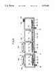
- FIG. 11illustrates a prior-art apparatus for sputter-forming thin layer on a semiconductor substrate.
- the apparatusincludes a chamber 1 which are divided by partition walls into a loading compartment 3, and an etching compartment 4, a depositing compartment 5 and an unloading compartment 6.
- the partition wallsare provided with passage openings to be covered with lock valves 2a, 2b and 2c, respectively.
- the loading compartment 3is equipped with an inlet 7a for nitrogen gas, and an exhaust outlet 8. Provided within the loading compartment 3 is a belt conveyer 9a as transport means.
- the etching compartment 4is equipped with an inlet 10a for argon gas and an exhaust outlet 8b. Housed within the etching compartment 4 are a belt conveyer 9b and a substrate support 11a with a tray 12 for accommodating a semiconductor substrate attached thereto.
- the substrate support 11ais coupled to a radio frequency source 14 through a matching circuit 15, and is electrically insulated from the chamber 1 by an insulation 16a.
- the depositing compartment 5is also provided with an inlet 10a for argon gas and an exhaust outlet 8c. Housed within the depositing compartment are a belt conveyer 9c, a substrate support 11b and a target 17.
- the target 17is connected to a DC source 18 which applies a high potential voltage across the target 17 and the argon gas atmosphere within the depositing compartment.
- An insulation 16belectrically separates the substrate support 11b from the chamber 1, and another insulation 16c provides an electrical insulation between the target 17 and the chamber 1.
- the unloading compartment 6is equipped with an inlet 7b for nitrogen gas, and an exhaust outlet 8d. It also houses a conveyer belt 9d.
- a thin layer of materialis formed on the semiconductor substrate as follows.
- All of the loading compartment 3, etching compartment 4, depositing compartment 5 and unloading compartment 6 in the chamber 1are first kept in a high-intensity vacuum state. Then nitrogen gas is introduced into the loading compartment 3 via the gas inlet 7a thereby to attain the atmospheric pressure within the loading compartment.
- a plurality of silicon substratesare carried into the loading compartment through an entry opening (not shown), after which the entrance opening is closed with a cover lid (not shown). It should be noted that the silicon substrate has been cleaned with a solution but has already an oxide film grown on its surface.
- the loading compartment 3is exhausted through the outlet 8a using a vacuum pump (not shown) thereby to produce a high-intensity vacuum within the compartment.
- the lock valve 2aWith the loading compartment in this high vacuum state, the lock valve 2a is swung open and the tray 12 carrying the silicon substrates is transferred through the passage opening in the partition into the neighboring etching compartment 4 by means of the belt conveyer 9a. Thereafter, the lock valve 2a is moved back to its passage closing position.
- the operations of both the belt conveyer 9a and the movable lock valve 2aare controlled by suitable externally provided control unit such as a switching unit.
- the etching compartment 4is kept at a high vacuum of 10 -7 -10 -8 Torr.
- an argon gasis introduced into the deposit compartment at 10 -3 -10 -1 Torr, followed by switching the RF source 14 into operation.
- the RF source 14applies a high potential of several hundred to several thousand volts across the silicon substrate 13 and the argon atmosphere within the compartment to produce an argon plasma.
- Excited argon ions in the plasmabombard the silicon substrate kept at a negative potential.
- the bombarding argon ionsact to sputter-etch the naturally grown oxide film of the surfaces of the silicon substrate 13.
- the supply of the argon gas and the high potentialare both discontinued.
- the remaining argon gasis expelled out of the etching compartment 4 to keep the compartment in a high vacuum state.
- the lock valve 2bis swung open to allow the substrate carrying tray 12 to be transported into the deposit compartment 5 by the belt conveyer 9b.
- a second tray with a plurality of silicon substrateis carried into the etching compartment 4.
- the deposit compartment 5has also been maintained at a high vacuum of 10 -7 -10 -8 Torr.
- argon gasis introduced into deposit compartment at 10 -3 -10 -1 Torr through the inlet 10b.
- the DC power supply 18is turned on to apply a potential of several hundred to several thousand volts across the target 17 and the argon gas in the compartment, thereby creating argon plasma.
- Highly excited argon ions in the plasmabombard the target 17 which is kept at a negative potential and strike atoms off the surface of the target.
- a thin layer having a uniform and homogeneous qualityis deposited on the surface of the silicon substrate.
- the supply of the argon gas as well as the high potential voltageis discontinued.
- the deposit compartment 5is again exhausted to a high vacuum state.
- the lock valve 2cis moved to an open position and the belt conveyer 9c carries the tray 12 with the silicon substrate 13 into the unloading compartment 6. Thereafter, the lock valve 2c is swung back to the closed position. At about the same time, the second tray is brought into the deposit compartment 5, while a third tray into the etching compartment 4. In this manner, the trays with silicon substrates are moved through the etching and deposit compartment into the unloading compartment 6 one after another. In the unloading compartment 6, the silicon substrate 13 on each tray are loaded off into a container (not shown). When the silicon substrates on all of the trays have been loaded into the container, the unloading compartment 6 is restored to the atmospheric pressure and the substrate-filled container is carried out of the unloading compartment to a next process location.
- This inventionhas been made to overcome the above-stated drawbacks of the prior-art, and it is an object of the invention to provide a method and apparatus for forming a thin layer of material on a semiconductor substrate without exposing to the surrounding atmosphere immediately after the removal of undesired organic contaminants and a naturally grown oxide film from the substrate surface at relatively low temperatures without relying on solvent cleaning and without causing damage to the substrate surface.
- the present inventorshave long been engaged in the research on forming thin layers of material on the surface of a semiconductor substrate.
- the organic contaminants on the substrate surfaceare disintegrated and dissipated and, at the same time, a very thin film of oxide naturally grows on the cleaned substrate surface, and that the naturally grown oxide film can be removed by heating the substrate in the presence of an etching gas under exposure to light.
- the discoverieshave lead to the present invention.
- the inventionis directed to a method for removing organic contaminants and the like from the surface of a semiconductor substrate and for forming a thin layer of material on the cleaned substrate surface.
- the method of the inventionincludes the steps of: preparing a semiconductor substrate; growing a thin layer of oxide by heating the semiconductor substrate in the presence of oxidizing gas and under exposure to light while removing organic contaminants on the substrate surface in the process; exposing an underlying cleaned surface of the semiconductor substrate by removing the oxide film on the substrate surface; and forming a thin layer of material on the exposed clean surface of the substrate without exposing it to the ambient air.
- Oxidizing gases suitable for use in the inventionare O 3 , O 2 , N 2 O, and NF 3 .
- the oxide film on the semiconductor substratemay be removed by heating the substrate in the presence of an etching gas and under exposure to light. With this procedure, the oxide film is stripped at relatively lowered temperatures without causing any damage to the substrate surface.
- the gas for etching the oxide filmpreferably includes hydrogen chloride gas, chlorine gas and hydrogen gas.
- the thin filmmay he formed on the cleaned surface of the substrate by any suitable process but the chemical vapor deposition and sputter deposition are preferred.
- CVD layersmay include: a silicon layer such as monocrystalline silicon layer, a polycrystalline silicon layer; an insulating layer such as a silicon nitride layer and a silicon oxide layer; a layer of high melting point metal such as tungsten, molybdenum, tantalum and titanium; and a layer of a silicide compounds of the stated high melting point metals.
- Any suitable thin layer of materialmay be formed by sputter-deposition and it may includes electrically conductive as well as insulating layers.
- the semiconductor substratemay preferably be heated up to temperatures between 200°-700° C.
- temperatures below 200° C.the oxide film is removed from the substrate surface at too slow a rate, while a temperatures above 700° C., the oxide film is etched first enough but only at the expense of causing the thermal fusion of the types stated previously.
- the step of etching the oxide layerinvolves carrying a semiconductor substrate into a first chamber and filling the first chamber with a gas for etching the oxide film.
- the step of forming a thin film of material on a semiconductor substrateinvolves carrying the semiconductor substrate from the first chamber into a second chamber, and filling the second chamber with a gas suitable for forming the thin film.
- a third chamber which is exhausted of the airmay optionally be provided between the first and second chamber. The semiconductor substrate which has gone through the oxide film removal in the first chamber is brought into the third chamber before it is moved on into the second chamber for the formation of the thin layer.
- the step of etching the oxide layer away from a semiconductor substrateinvolves carrying the semiconductor substrate into a chamber and filling the chamber with a gaseous atmosphere suitable for etching the oxide film.
- the step of forming a thin layer of materialinvolves replacing the etching gas atmosphere in the chamber with a gaseous atmosphere suitable for forming the thin layer of material.
- Light used in the present inventionmay preferably be UV light emitted from a low-pressure mercury lamp, high high-pressure mercury lamp, a mercury-xenon lamp and an excimer laser source.
- An apparatus for forming a thin layer of materialincludes; a chamber for accommodating a semiconductor substrate; means for growing an oxide layer on the surface of the semiconductor substrate which is placed in the chamber; means for stripping the oxide layer of the substrate surface; and means for forming a thin layer of material on the substrate surface which has been cleaned of the oxide film.
- Means for growing the oxide layer on the substrate surfaceincludes for introducing oxidizing gas into the chamber, a first heating means for heating the semiconductor substrate placed in the chamber, and a first light means for radiating light rays to the surface of the semiconductor substrate.
- Means for stripping the oxide film according to the inventionpreferably includes means for introducing into the chamber a gas for etching the oxide film, a second means for heating the semiconductor substrate within the chamber, and a second light means for radiating light rays for the surface of the semiconductor substrate.
- Any suitable meansmay be employed for forming a thin layer of material.
- Chemical vapor deposition means and sputter deposition meansare preferred for the purpose.
- the chamberhas a compartment for forming an oxide layer, a compartment for removing the oxide layer, and a compartment for forming a thin layer of material.
- Means for forming an oxide layeris provided in the oxide forming compartment, means for removing the oxide layer is provided in the oxide removing compartment, and means for forming a thin layer of material is provided in the layer forming compartment.
- the apparatusalso has conveyer means for carrying the semiconductor substrate successively through these three compartments.
- the apparatusmay preferably be provided with an auxiliary and intermediate compartment between the oxide removing compartment and the layer forming compartment through which the semiconductor substrate is carried from the oxide removing compartment and to a layer forming compartment by conveyer means.
- An apparatusincludes a chamber which comprises a front compartment and a rear compartment.
- the front compartmentis provided with means for forming the oxide layer, while the rear compartment with the means for removing the oxide layer as well as the means for forming the thin layer of material.
- the apparatusitself is equipped with a conveyer for carrying the semiconductor substrate from the front compartment to the rear compartment.
- the means for removing the oxide filmincludes means for introducing into a rear compartment a gas suitable to etch away the oxide film, a second means for heating the semiconductor substrate placed in the rear compartment, and a second light means for radiating light rays toward the surface of the semiconductor substrate.
- the means for forming the thin layer of materialincludes means for sputtering particles out of a target onto semiconductor substrate to form a thin layer thereon.
- the rear compartmentis equipped with a substrate carrier for moving the semiconductor substrate within the rear compartment.
- the substrate carriermoves the semiconductor substrate to a position where the substrate surface faces the second light means when the oxide layer on the substrate surface is to be removed, and to a position where the substrate surface faces the target when the thin layer is to be formed on the substrate surface.
- FIGS. 1A-1Dare sectional views of a semiconductor substrate in successive steps in a method according to the invention.
- FIG. 2is a cross-sectional view of an apparatus for forming a thin layer of material according to one preferred embodiment of the invention
- FIGS. 3A and 3Bare graphic representations which indicate whether an oxide film formed on a semiconductor substrate is removed or not;
- FIG. 4is an Arhenious plot showing relations between etching rates of a silicon substrate and temperature at which the silicon substrate is heated;
- FIGS. 5A-5Care schematic illustrations of a semiconductor substrate showing a procedure for determining the etching rate of a silicon substrate
- FIG. 6is a cross-sectional view of an apparatus for forming a thin layer of material on a semiconductor substrate according to another preferred embodiment of the invention.
- FIG. 7is a cross-sectional view of an apparatus for forming a thin layer of material on a semiconductor substrate according to still another embodiment of the invention.
- FIG. 8is a cross-sectional view of an apparatus for forming a thin layer of material on a semiconductor substrate according to still another embodiment of the invention.
- FIGS. 9A and 9Bare cross-sectional views of an apparatus for forming a thin layer of material on a semiconductor substrate according to still another embodiment of the invention.
- FIGS. 10A and 10Bare cross-sectional views of an apparatus for forming a thin layer of material on a semiconductor substrate according to still another embodiment of the invention.
- FIG. 11is a cross-sectional view of a prior-art apparatus for forming a thin layer of material on a semiconductor substrate.
- a semiconductor substrate 13such as a silicon substrate is placed in an oxidizing gas atmosphere and under exposure to UV light, thereby to induce a photo-chemical reaction on the surface of the semiconductor substrate.
- unwanted organic contaminants 20 on the substrate surfaceare disintegrated and removed on one hand (FIG. 1A), and a thin oxide film 21 is grown on the substrate surface (FIG. 1B) on the other.
- the oxide filmeffectively contains an undesired metal layer and damaged surface layer.
- the oxide-clad silicon substrate 13is subjected to hydrogen chloride gas or chlorine gas under UV ray radiation, thereby eliminating the oxide film 21 on the substrate surface, and exposing the cleaned substrate surface.
- the silicon substrate 13is next coated with a thin layer of material over its cleaned surface by chemical vapor deposition or CVD without being exposed to the ambient air.
- the interface between the substrate 13 and the thin layer 22 in the resultant semiconductor deviceis free of undesirable organic contaminants, naturally grown oxide, metal layer or damage layer i.e. the interface is well controlled and conditioned.
- FIG. 2there is illustrated a novel apparatus for forming a thin layer on the semiconductor substrate according to one embodiment of the invention.
- the apparatusincludes a chamber 1 which is lined with an anti-corrosive material.
- the chamber 1is divided into three compartments 23, 24 and 25 by partition walls.
- the partition wallshave formed therein passage openings which are covered with lock valves 2a and 2b, respectively.
- the first compartment 23is for forming an oxide layer on a semiconductor substrate and is provided with a gas inlets 30 for introducing oxidizing gas, a belt conveyer 9a for moving the semiconductor substrate, and a window 26a for passing UV rays therethrough.
- a low-pressure mercury lamp 27ais disposed in facing relations with the UV window 26a.
- the first compartment 23also houses a substrate support 11a on which a semiconductor substrate such as silicon substrate 13 is placed.
- the substrate support 11ais equipped with a heater unit 28a for heating the silicon substrate 13 on the support 11a.
- the second compartment 24is for removing the oxide layer from the semiconductor substrate and is furnished with a gas inlet for introducing a gas effective to etch the oxide layer away, a belt conveyer 9b for moving the silicon substrate, and a window 26b for letting in UV light. Disposed face-to-face to the window 26b is a low-pressure mercury lamp 27b.
- the second compartment 24also houses a support 11b on which the silicon substrate is placed. The substrate support 11b is equipped with a heating unit 28b.
- the third compartment 25is for forming a thin layer on the silicon substrate and it is equipped with an exhaust outlet 8 and inlets 29a, 29b for introducing reactive gases.
- the compartment 25balso houses a conveyer 9c and a substrate support 11c.
- the substrate support 11cis furnished with a heating unit 28c.
- An untreated silicon substrateis positioned on the support 11a in the first compartment 23 for forming the oxide film. Since the silicon substrate 13 has not been subjected to a solvent cleaning, its surface may be coated with an unwanted layer such as an oxide layer and a metal layer. Or else, the substrate has a damaged surface (as shown in FIG. 1A).
- an oxidizing gassuch as ozone, N 2 O or NF 3 is introduced into the compartment through the inlet 30.
- the low-pressure mercury lamp 27ais turned on to radiate UV light into the compartment through the window 26a, and at the same time the heater unit 28a is put into operation to heat the silicon substrate 13 up to a temperature of 300° C., at which temperature organic contaminants that may be present on the substrate surface are dissipated by a chemical oxidation process.
- the silicon substrate 13is further heated up to temperatures between 500°-800° C., and a thin oxide layer grows on the substrate surface as a result of photo-chemical reaction.
- the oxide layereffectively contains an undesired metal layer disposed on the substrate and a damaged substrate surface caused in a preceding step (see FIG. 1B).
- the lock valve 2aAfter forming the oxide film on the surface of the silicon substrate 13 in the first compartment 23, the lock valve 2a is swung open and both belt conveyers 9a and 9b are put into motion to carry the silicon substrate 13 with the oxide film formed thereon into the second compartment 24 for removing the oxide layer.
- HCl gas for etching the oxide layeris introduced via the gas inlet 31, and the low-pressure mercury lamp 27b is turned on to direct UV light rays into the compartment 24.
- the silicon substrate 13is heated up to temperatures between 200°-700° C. by the heating unit 28b. Under the conditions, the oxide layer is etched away from the surface of the silicon substrate 13, leaving the cleaned substrate surface (see FIG. 1C).
- the silicon substrate 13must be heated as high as 1,000°-2,000° C.
- the oxide layer on the substrate surfaceis effectively removed at relatively low temperatures of 500°-800° C. The same is true when chloride gas is used.
- the process of forming the oxide layer on the silicon substrate 13 in the first compartment 23 and the process of etching the oxide layer on the substrate 13 in the second compartment 24 which corresponds to the steps represented in FIGS. 1A-1C,are hereinafter referred in combination to as a photo-chemical cleaning process or step.
- the next processinvolves moving the lock valve 2b to its open position, and carrying the photo-chemically cleaned silicon substrate 13 into the third compartment 25 by means of the belt conveyers 9b and 9c.
- the cleaned silicon substrate 13is placed on the support 11c.
- the compartment 25is first exhausted through the outlet 8 and then supplied with a reactive gases for performing chemical vapor deposition through the gas inlets 29a and 29b, while heating semiconductor substrate with the heater unit 28c.
- a thin CVD layeris formed on the surface of the silicon substrate 13. With the organic contaminants, naturally grown oxide layer, metal layer and damaged surface layer all having been etched away from the substrate surface, the newly formed CVD layer involves a well-controlled and well-conditioned interface with the silicon substrate 13 (see FIG. 1D).
- the CVD layermay include a mono-crystalline silicon layer epitaxially grown on the silicon substrate, polycrystalline silicon layer and an amorphous silicon layer.
- the desired epitaxial layeris obtained by heating the semiconductor substrate at relatively low temperatures around 600° C. with no oxide film naturally grown at the interface with the substrate. Also, with no unwanted metal layer and damaged surface layer on the semiconductor substrate, the epitaxially grown silicon layer has extremely good crystal grain structure, and thus very low contact resistance.
- the resulting polysilicon layerexhibits a low contact resistance with respect to the underlying silicon substrate.
- the polysilicon layerrenders itself an excellent and stable electrical interconnection.
- Ultra-thin insulating layers of, for example, oxide) silicon, nitride silicon which are suitable for gate insulation and capacitor insulationare successively formed by CVD technique according to the invention with no naturally grown oxide film present at their interface with the substrate surface.
- the naturally grown oxide filmis very fragile, inferior in quality and has low voltage resistant insulation.
- the silicon oxide layer and the silicon nitride layerare formed on the silicon substrate according to the invention, there exists no such naturally grown oxide film between the deposited layers and the substrate, which leads to the manufacture of a semiconductor device with much improved insulating characteristics.
- the silicon nitride layer thus formedexhibit extremely good insulating performance, including di-electric property.
- high melting point metalssuch as tungsten, molybdenum, tantalum and titanium, and the silicide may be chemically vapor-deposited on the cleaned substrate surface.
- the chemical vapor deposition of the stated metals and metal silicideproduces a semiconductor device having an extremely low contact resistance without performing a heat treatment on the device.
- the procedureinvolves depositing an oxygen-free thin film such a silicon nitride film over the silicon substrate surface after it has been stripped off the natural oxide film, and then observing the element profile of spectrum in the direction of each thickness using Auger electron spectroscopic analysis With this technique, the presence of oxygen is determined at the interface between the silicon surface (Si) of the substrate and the deposited film of S 3 N 4 . The presence or absence of oxygen component at the interface indicates whether the spontaneous oxide film has been grown or not at the area.
- FIG. 3Arepresents Auger spectrum profiles of a sample silicon substrate taken in the direction of each thickness by the Auger electron spectroscopic analysis, the substrate being coated with a silicon nitride film by chemical vapor deposition or CVD. It is noted that the silicon nitride layer can be formed by means of the apparatus of FIG. 2 using SiH 2 Cl 2 and NH 3 as reaction gases.
- the ordinate axisrepresents the intensity of the Auger signal, while the coordinate axis the sputtering time. It can be seen that with the sample silicon substrate which has been pretreated with HCl gas to remove the oxide film, no Auger signal appeared at or in the neighborhood of the interface between the silicon substrate and the Si 3 N 4 film that may indicate the presence of oxygen.
- the sample substrateswere subjected to dry etching in the presence of hydrogen chloride under exposure the UV light and at varying temperatures.
- the etching rates of the silicon substrateswere observed at different temperatures and the observed etching rates were plotted in logarithm against the reverse temperatures 1/T on an Arhenius chart as shown in FIG. 4. It is noted that the rate of the etching on the silicon substrate was determined instead of the naturally grown oxide film since the oxide film is too thin to sense etch removal rate. It is assumed that the etching rate of the silicon substrate suggests the rate at which the oxide film is being removed.
- FIGS. 5A-5CBefore going on into a detailed discussion of the Arhenius plot of FIG. 4, the procedure used to detect the etching rate of the silicon substrate is first explained with reference to FIGS. 5A-5C.
- FIG. 5Atwo P-type silicon substrates 33 having a resistance of 1-100 ⁇ .cm were prepared and coated with an oxide mask 32. Etching was performed on the coated substrate while supplying 100% HCl gas at 700 sccm and keeping the ambient pressure at 7.2 Torr (FIG. 5B). One substrate was under the radiation of the UV light from a low-pressure mercury lamp during etching, whereas the other was not. After removing the oxide film 32, the etch depth d on the substrate was determined, from which the etching rate was obtainable through calculation (FIG. 5C).
- etching rate with the sample silicon substrate at various temperatureswere obtained with (A) or without (B) the radiation of the UV light.
- the obtained etching rateswere plotted as a function of temperature on the Arhenius chart of FIG. 4.
- the etching rategradually increases over the range from room temperature to 200° C. Above 200° C., the etching rate is seen jumping up. The abrupt transition of the etching rate at 200° C. manifests that etching is actually proceeding on the substrate at temperature above 200° C., while below 200° C. no appreciable etching is taking place.
- FIG. 4is also shows that the etching rate fails to rise even if the substrate is heated up to as high as 600° C. unless under the radiation of the UV light. In other words, no substantial etching takes place even at elevated temperatures without the UV radiation.
- the conditions under which the etching of the silicon substrate was observedare similar to those employed for removing the naturally grown oxide film from the silicon substrate. Thus, the findings obtained from the experiment are applicable to the removal rates of the naturally grown oxide film.
- the substrate materialis preferably heated at temperatures below 600° C.
- the polysilicon substrate of this typemay be heat-treated at temperatures above 600° C. and still shows satisfactory performance and properties as the semiconductor substrate.
- a heat treatment of the polysilicon substrate at elevated temperatureshas an advantage that it can remove the naturally grown oxide film at a faster rate. But care should be taken that the polysilicon substrate is not heated up to temperatures exceeding 700° C. where the above stated advantage is offset by a disadvantage that near amorphous silicon is turned into polysilicon.
- the semiconductor substratemay preferably be heat-treated at temperatures within the range 200°-700° C.
- FIG. 6there is illustrated an apparatus for forming a thin layer of material on a semiconductor substrate according to another preferred embodiment of the invention.
- the apparatus of FIG. 6is substantially identical in construction and function to that shown in FIG. 2 except that it is provided with an intermediate compartment 34 auxiliary to the third compartment 25 between the second compartment 24 and the third compartment.
- corresponding partsare designated by corresponding reference numerals, giving no further detail description thereof.
- the auxiliary compartment 34houses a substrate support 11d and a belt conveyer 9d.
- a silicon substrate 13 which has been stripped of the oxide layer in the second compartmentis carried by the conveyer 9b through the passage opening in the partition into the auxiliary compartment 34.
- the lock valve 2bhas to be swung open in an advance.
- the belt conveyer 27 in the auxiliary compartment 34is put into operation and the lock valve 2c is driven open to transport the silicon substrate 13 through the auxiliary compartment 34 into the third compartment 25.
- the lock valve 2cis again moved back to the closed position. In this manner, there is very little likelihood that the etching gas in the second compartment 24 is undesirably mixed with the reactive gases in the third compartment 25, eliminating the possibility of the second compartment being polluted with the gases used in the third compartment and vice versa.
- FIG. 7there is shown an apparatus according to still another embodiment of the invention.
- the apparatusincludes a front compartment 35 and a rear compartment 36.
- the front compartment 35being the same in structure as the first compartment 23 in the apparatus of FIG. 2, has its component parts indicated by similar reference numerals, and no detailed description is given here.
- the rear compartment 36is provided with a gas inlet 31 for etching gas, an exhaust outlet 8, and gas inlets 29a and 29b for reactive gases.
- the rear compartment 36is also equipped with a conveyer 9b for transporting a semiconductor substrate, and a window 26b for letting in the UV rays.
- a low-pressure mercury lamp 27bis disposed outside the compartment 36 and opposite the window 26b.
- a substrate support 11bfor supporting a silicon substrate 13.
- the support 11bis equipped with a heater unit 28b.
- a thin layer of materialis formed on the silicon substrate in the following fashion.
- a silicon substrate 13is first positively coated with an oxide layer as explained in connection to FIG. 2. Then, the lock valve 9a is opened to allow the coated silicon substrate 13 to be transported into the rear compartment 36 by means of the conveyers 9a and 9b. The lock valve 9b is returned to its closed position, and HCl gas for etching the oxide layer is introduced into the compartment 36 through the inlet 31. At the same time, the mercury lamp 27b is turned on to direct the UV radiation into the compartment, which heats the silicon substrate up to temperatures between 200°-700° C. Under the circumstances, the oxide film on the silicon substrate is etched away, leaving a cleaned substrate surface. Upon the removal of the oxide layer, the rear compartment 36 is exhausted by the exhaust outlet 8.
- the cleaned silicon substrate 13is again heated by the heater unit 28b, while introducing reactive gases for chemical vapor deposition into the compartment 36 through the inlets 29a and 29b. As a result, a thin CVD layer is formed on the surface of the silicon substrate 13.
- the apparatus of FIG. 7is advantageous in that it is very compact in size.
- FIG. 8An apparatus according to a still another preferred embodiment of the invention is illustrated in FIG. 8.
- the illustrated apparatusincludes a first compartment 23 for forming an oxide layer, a second compartment 24 for etching the oxide layer, and a third compartment 25 for forming a thin CVD layer.
- Both the first and second compartments 23 and 24are similar in construction to those in the apparatus of FIG. 2. Thus, corresponding parts are indicated by corresponding reference numerals.
- a distinctive featureis that the third compartment 25 is designed for sputter-deposition of a thin layer.
- the compartment 25has a gas inlet 10 for argon gas, and a exhaust outlet 8 formed in the surrounding wall.
- the compartment 25also houses a conveyer 9c, a target 17 and a substrate support 11c.
- the target 17is coupled to a DC source 18 for applying a high potential voltage between the target 17 and the argon atmosphere in the compartment.
- the substrate support 11cis electrically insulated from the compartment by an insulation 16b, while the target 17 by an insulation
- a silicon substrate 13has been stripped of an oxide layer on its surface in the second compartment 24.
- the lock valveis open, and the conveyers 9b and 9c are put into operation to carry the stripped silicon substrate 13 into the third compartment 25.
- the compartment 25is exhausted through the outlet 8 by a vacuum pump (not shown) to create a high vacuum state of around 10 -7 -10 -8 Torr.
- argon gasis introduced into the compartment 25 via the inlet 10 at a pressure of 10 -3 -10 -1 Torr, followed by the application of a high potential voltage between several hundred and several thousand volts across the target 17 and the argon gas in the compartment by means of the DC source 18. Consequently, plasma is induced.
- High high-energy argon ions in the plasmabombard the target 17 which is at a negative potential. Bombarding ions strikes atoms off the target, which are then deposited on the silicon substrate to form a thin suppered layer.
- the apparatusincludes a front compartment 35 and a rear compartment 36.
- the front compartment 35being essentially the same in construction and function as the first compartment 23 in the apparatus of FIG. 2, like parts are indicated by like reference numerals, and no detailed description is given.
- the rear compartment 36is equipped with a gas inlet 31 for oxide etching gas, a gas inlet 10 for argon gas, and an exhaust outlet 8.
- a window 26bfor letting in the UV light radiated by a low-pressure mercury lamp 27, which is positioned opposite the window 26b outside the compartment.
- the rear compartment 36houses a substrate support 11b and a target 17.
- the substrate support 11bhas a heating unit 28b, while the target 17 is coupled to a DC power source 18.
- An insulation 16electrically insulate the target 17 from the compartment 36.
- the rear compartment 36also has a platen 37 which is supported by a shaft 38 for rotation.
- a tray 39 for accommodating a silicon substrate 13is fixedly attached to the rotatable platen 37.
- the tray 39has formed thereon a substrate stops 40 in the form of a small projection.
- the rotatable platen 37is held horizontally on support pins 41 with the silicon substrate 13 facing squarely the mercury lamp 27b.
- the platen 37When it is desired to use the rear compartment 36 for forming a thin layer of material on the silicon substrate 13 as shown in FIG. 9B, the platen 37 is rotated on the shaft 38 until the silicon substrate 13 on the tray 39 faces squarely the target 17. In an inclined position of the platen 37, the silicon substrate 13 tends to slide down on the tray 39, but the projection 40 serves to prevent its fall-down.
- a thin layer of materialis formed on a semiconductor substrate as follows.
- the silicon substrate 13is coated with an oxide layer as in the apparatus of FIG. 2.
- the lock valve 2ais swung open, and the silicon substrate 13 with the oxide coating is transferred from the front compartment 35 to the rear compartment 36 by means of the conveyers 9a and 9b.
- the transfer silicon substrate 13is placed on the trays 39 on the horizontally held platen 37.
- HCl gasis introduced into the compartment 36 through the etching gas inlet 31, followed by the energization of the mercury lamp 27b.
- the operating mercury lamp 27bradiates UV light through the surface of the silicon substrate 13 through the window 26b.
- the heater unit 28bis put in action to heat the silicon substrate up to temperatures between 200°-700° C.
- the simultaneous application of heat and lightdisintegrates and dissipates the oxide layer on the substrate.
- the supply of HCl gas and the radiation of the UV light by mercury lamp 27are discontinued, and the compartment 36 is exhausted of HCl gas to keep in a high vacuum condition.
- the platen 37is rotated upward on the shaft 38 until the silicon substrate 13 on the tray 39 squarely faces the target 17.
- argon gasis introduced into the compartment 36 through the inlet 10, and a high potential is applied across the target 17 and the argon atmosphere thereby to produce plasma in the compartment.
- the argon ions in the plasmabombard the target 17 with high energies and sputter atoms off the target to be deposited on the silicon substrate 13.
- a resultis a semiconductor device having a thin sputtered layer on a silicon substrate with a well-conditioned interface between them.
- FIGS. 10A and 10Ban apparatus according to a still another embodiment of the invention is shown in vertical and horizontal cross-sections.
- the illustrated apparatusis particularly suitable for a batch processing of many semiconductor substrates, and includes a chamber 1 which is lined with an anti-corrosive material and is divided by partition walls into a first compartment 23 for forming an oxide layer on a semiconductor substrate; a second compartment 24 for etching away the oxide layer; and a third compartment 25 for forming a thin layer of material.
- the partition wallsare each formed with a passage opening which are closed by shield doors 2b and 2c.
- the first compartment 23is provided with an entrance opening for semiconductor substrates to be processed, which is normally close by a shield door 2a.
- the first compartment 23is also equipped with a gas inlet 30 for oxidizing gas and a window 26a for letting in UV light radiated from a low-pressure mercury lamp 27a, which is disposed outside the chamber 1 in facing relations with the window 26a.
- the first compartment 23houses a support block 11a, on which a boat 42 for holding a silicon substrate is detachably attached. As shown, the boat is of construction to removably hold a plurality of silicon substrates to be processed.
- the boat 42is a cylindrical structure with a plurality of vertical grooves 42 formed spaced apart in its peripheral wall.
- each of the vertical grooves 43Formed in each of the vertical grooves 43 are a plurality of horizontal slots 43 spaced apart in a vertical direction.
- the horizontal slot 43fittingly accommodate the silicon substrate 13.
- the support block 11ais rotatable on its axis and is equipped with a heating unit 28a.
- the second compartment 24 for etching the oxide layerhas a gas inlet 31 for an etching gas, and is formed with a window 26b for allowing the UV rays from a low-pressure mercury lamp 27b to pass into the compartment.
- the mercury lamp 27bis disposed outside the compartment 24 and opposite to the window 26b.
- the compartment 24houses a support block 11b, on which the boat 42 is removably attached.
- male connectors 45are provided on the upper supporting surface of the support block 11b, and their mating female connectors are formed at the bottom of the boat 42 although they can not be seen in FIG. 10A.
- the support block 11bhas a heating unit 28b and is rotatable on its axis.
- the third compartment 25 for forming a thin CVD layer on the silicon substrateis provided with an exhaust outlet 8 and inlets 29a and 29b for reactive CVD gases.
- the compartment 25is also formed with an exit opening for process silicon substrates, which is normally closed by a shield door 2d.
- the compartment 25houses a support block 11c for detachably supporting the boat 42.
- the support block 11chas male connectors 45 provided on its top support surface, which fit into the mating female connectors on the bottom of the boat 42.
- a pair of retractable transfer rods 9are provided in the apparatus.
- the rods 9are extended into the chamber 1 below the boat 42, lift up the boat and then move the boat into the desired compartment.
- the rods 9are retracted away from the chamber 1, so that they may not interfere the accompanying rotation of the boat 42.
- the method of the inventionis performed with the apparatus as follows.
- a plurality of silicon substratesare loaded onto the boat 42.
- the shield door 2a for the entrance openingis open and the boat 42 loaded with the silicon substrate is carried into the first compartment 23 by the transfer rods 9.
- the boat 42is fixedly positioned on the support block 11a by means of the mating connectors.
- the retractable transfer rods 9are withdrawn out of the chamber, and, while rotating the support block 11a on its axis, an oxidizing gas such as oxygen, and NF 3 is supplied into the compartment through the gas inlet 30.
- the mercury lamp 27a and the heater unit 28are put into operation, the former radiating UV light into the compartment via the window 26a, the latter heating the silicon substrate up to temperatures between room temperature and 300° C.
- silicon substrates 13Under the circumstances, organic contaminants that might be present on the surfaces of the silicon substrates 13 are disintegrated and dissipated by oxidation.
- the silicon substratesare further heated up to temperatures between 500°-800° C., where a photo-chemical reaction acts to coat the silicon substrates with very thin oxide layers.
- the oxide layerscontain unwanted metal layers on the substrate surfaces or damaged substrate surfaces.
- Next stepinvolves opening the shield door 2b and carrying the boat 42 on the transfer rods 9 into the second compartment 24, where the boat 42 is fixedly placed on the support block 11b.
- the support block 11bis started to rotate, and the shield door 2b is closed back.
- HCl gasis introduced into the compartment 24 through the inlets 31.
- the mercury lamp 27b and the heater unit 28bare placed into operation.
- the mercury lamp 27bdirects the UV light into the compartment, while the heater unit 28b heats the silicon substrates up to temperatures between 200°-700° C. At the stated elevated temperatures, the thin oxide layers on the substrate surfaces are etched away, leaving the surfaces of the silicon substrate 13 cleaned.
- the boat 42After opening the shield door 2c, the boat 42 is carried over into the third compartment 25 in a similar manner, where it is fixedly position on the support block 11c.
- the shield door 2cis returned to its closed position, the transfer rods 9 are retracted, and the support block 11c is rotated, followed by exhausting the compartment 25 through the exhaust outlet 8.
- reactive gases for chemical vapor depositionare introduced through gas inlets 29a and 29b, thereby to deposit thin CVD layers on the silicon substrates.
- the CVD layer on the semiconductor substrate 13has a well-conditioned interface with the substrate surface.
- the apparatus of FIGS. 10A and 10Bare particularly suited to process a large number of silicon substrates.
- the method according to the inventionis effective to remove organic contaminants, unwanted metal layers and damaged surface layer which are present on a semiconductor substrate, and to form a thin layer of material on the substrate surface without exposing it to the surrounding air.
- the apparatus of the inventionis capable of forming a thin layer of material on the surface of a semiconductor substrate without exposing it to the ambient atmosphere successively and right after the substrate surface has been stripped of an oxide layer. Consequently, a semiconductor device with a thin layer of material having improved quality and a well-conditioned interface with the substrate is obtained according to the present invention.
Landscapes
- Engineering & Computer Science (AREA)
- Physics & Mathematics (AREA)
- Microelectronics & Electronic Packaging (AREA)
- General Physics & Mathematics (AREA)
- Manufacturing & Machinery (AREA)
- Computer Hardware Design (AREA)
- Condensed Matter Physics & Semiconductors (AREA)
- Power Engineering (AREA)
- Chemical & Material Sciences (AREA)
- Chemical Kinetics & Catalysis (AREA)
- Electromagnetism (AREA)
- Materials Engineering (AREA)
- Drying Of Semiconductors (AREA)
Abstract
Description
This application is a division of application Ser. No. 07/317,710 filed Mar. 1, 1989.
1. Field of the Invention
This invention relates to a method for forming a thin layer of material on the surface of a semiconductor substrate and an apparatus for the same. In particular, this invention relates to a novel method for forming a thin layer of material on the surface of a semiconductor substrate after the substrate surface ha been cleared of unwanted organic contaminants, metal contaminants and damaged surface, and without exposing the cleaned substrate surface to the ambient air, and an apparatus for carrying out the method.
2. Description of the Background Art
Performance characteristics of electronics devices are readily and adversely affected by contaminants introduced on purpose or by accident in the course of the manufacturing process. In order to avoid any introduction of contaminants into the electronics products as much as possible, it is necessary to keep the whole manufacturing environment at a maximum possible degree of cleanness. In this connection, highly advanced cleaning and purifying technologies are employed to produce desired starting materials and processing environments for the manufacture of the devices.
The manufacturing process for semiconductor devices is roughly divided into a thin film formation and a circuit pattern formation. The process for forming thin films or layers of material on the semiconductor substrate is further divided into many subprocesses depending on the material of which the thin films are made and techniques to be used to form them. Various cleaning technologies for each of the subprocesses or to be shared by some of the subprocesses have been developed into practical use. Important and essential to all these subprocesses is the pretreatment of the semiconductor substrate which is performed prior to forming the thin films on the substrate.
In the pretreatment process, the semiconductor substrate is cleaned with water, acid or alkalis or it is subjected to chemical oxidation or treatment with diluted hydrofluoric acid solution for the removal of grease heavy metals, naturally grown oxide film and the like. These solution cleaning techniques are widely used in the industry but are disadvantageous in that the cleaned semiconductor substrate is unavoidably exposed to the surrounding air before it is coated with thin films in a subsequent process. The exposure to the air causes a thin oxide film to grown on the substrate surface, especially when the substrate contains active semiconductor substance or it has exposed metal portions thereon. For this reason, the substrate cleaning with solutions falls short of complete cleaning of the substrate surface although it is effective to remove heavy metal and organic contaminants.
The growth of a natural oxide film on the semiconductor substrate has an adverse effect on the quality of various thin films to be formed on the substrate in subsequent steps. The thin films provided on the semiconductor substrate includes epitaxially grown layers, layers of high melting point metals or polysilicide layers, electrical interconnection layers, ultra-thin insulating layers. The formation of these layers on the semiconductor substrate is gaining a growing importance as the integration of semiconductor devices advances.
In order to have a brief background understanding, references is made to FIG. 11 which illustrates a prior-art apparatus for sputter-forming thin layer on a semiconductor substrate. As shown, the apparatus includes achamber 1 which are divided by partition walls into aloading compartment 3, and anetching compartment 4, a depositingcompartment 5 and anunloading compartment 6. The partition walls are provided with passage openings to be covered withlock valves
Theloading compartment 3 is equipped with aninlet 7a for nitrogen gas, and anexhaust outlet 8. Provided within theloading compartment 3 is abelt conveyer 9a as transport means.
Theetching compartment 4 is equipped with aninlet 10a for argon gas and anexhaust outlet 8b. Housed within theetching compartment 4 are abelt conveyer 9b and asubstrate support 11a with atray 12 for accommodating a semiconductor substrate attached thereto. Thesubstrate support 11a is coupled to aradio frequency source 14 through amatching circuit 15, and is electrically insulated from thechamber 1 by aninsulation 16a.
The depositingcompartment 5 is also provided with aninlet 10a for argon gas and anexhaust outlet 8c. Housed within the depositing compartment are abelt conveyer 9c, asubstrate support 11b and atarget 17. Thetarget 17 is connected to aDC source 18 which applies a high potential voltage across thetarget 17 and the argon gas atmosphere within the depositing compartment. Aninsulation 16b electrically separates thesubstrate support 11b from thechamber 1, and anotherinsulation 16c provides an electrical insulation between thetarget 17 and thechamber 1.
Theunloading compartment 6 is equipped with aninlet 7b for nitrogen gas, and anexhaust outlet 8d. It also houses aconveyer belt 9d.
With the apparatus, a thin layer of material is formed on the semiconductor substrate as follows.
All of theloading compartment 3,etching compartment 4, depositingcompartment 5 and unloadingcompartment 6 in thechamber 1 are first kept in a high-intensity vacuum state. Then nitrogen gas is introduced into theloading compartment 3 via thegas inlet 7a thereby to attain the atmospheric pressure within the loading compartment. A plurality of silicon substrates are carried into the loading compartment through an entry opening (not shown), after which the entrance opening is closed with a cover lid (not shown). It should be noted that the silicon substrate has been cleaned with a solution but has already an oxide film grown on its surface. Theloading compartment 3 is exhausted through theoutlet 8a using a vacuum pump (not shown) thereby to produce a high-intensity vacuum within the compartment. With the loading compartment in this high vacuum state, thelock valve 2a is swung open and thetray 12 carrying the silicon substrates is transferred through the passage opening in the partition into the neighboringetching compartment 4 by means of thebelt conveyer 9a. Thereafter, thelock valve 2a is moved back to its passage closing position. The operations of both thebelt conveyer 9a and themovable lock valve 2a are controlled by suitable externally provided control unit such as a switching unit. As stated above, theetching compartment 4 is kept at a high vacuum of 10-7 -10-8 Torr. With thesilicon substrate 13 on thetray 12 placed on thesupport 11a, an argon gas is introduced into the deposit compartment at 10-3 -10-1 Torr, followed by switching theRF source 14 into operation. As theRF source 14 is turned on, it applies a high potential of several hundred to several thousand volts across thesilicon substrate 13 and the argon atmosphere within the compartment to produce an argon plasma. Excited argon ions in the plasma bombard the silicon substrate kept at a negative potential. The bombarding argon ions act to sputter-etch the naturally grown oxide film of the surfaces of thesilicon substrate 13. Upon the complete removal of the oxide film, the supply of the argon gas and the high potential are both discontinued. The remaining argon gas is expelled out of theetching compartment 4 to keep the compartment in a high vacuum state. Under the conditions, thelock valve 2b is swung open to allow thesubstrate carrying tray 12 to be transported into thedeposit compartment 5 by thebelt conveyer 9b. At about the same time, a second tray with a plurality of silicon substrate is carried into theetching compartment 4. Thedeposit compartment 5 has also been maintained at a high vacuum of 10-7 -10-8 Torr. Now argon gas is introduced into deposit compartment at 10-3 -10-1 Torr through theinlet 10b. Then theDC power supply 18 is turned on to apply a potential of several hundred to several thousand volts across thetarget 17 and the argon gas in the compartment, thereby creating argon plasma. Highly excited argon ions in the plasma bombard thetarget 17 which is kept at a negative potential and strike atoms off the surface of the target. As a result of the process, a thin layer having a uniform and homogeneous quality is deposited on the surface of the silicon substrate. As the deposited layer grows to a desired thickness, the supply of the argon gas as well as the high potential voltage is discontinued. Then, thedeposit compartment 5 is again exhausted to a high vacuum state.
Thelock valve 2c is moved to an open position and thebelt conveyer 9c carries thetray 12 with thesilicon substrate 13 into theunloading compartment 6. Thereafter, thelock valve 2c is swung back to the closed position. At about the same time, the second tray is brought into thedeposit compartment 5, while a third tray into theetching compartment 4. In this manner, the trays with silicon substrates are moved through the etching and deposit compartment into theunloading compartment 6 one after another. In theunloading compartment 6, thesilicon substrate 13 on each tray are loaded off into a container (not shown). When the silicon substrates on all of the trays have been loaded into the container, theunloading compartment 6 is restored to the atmospheric pressure and the substrate-filled container is carried out of the unloading compartment to a next process location.
As has been stated hereinabove, with the arrangement of the conventional apparatus, it is necessary to apply a high potential voltage between the silicon substrate and the argon gas in order to remove the naturally grown oxide film from the substrate surface. However, the argon plasma generated by the high potential tends to cause damage on the surface of the silicon substrates.
It has also been proposed to gas-etch the natural oxide film on a semiconductor substrate through high temperature hydrogen reduction technique, followed by forming thin layers of desired metals. But the hydrogen reduction process exposes the semiconductor substrate to elevated temperatures normally above 1,000° C., causing thermal fusion at the PN junction. This in turn limits the application of the hydrogen reduction technique.
This invention has been made to overcome the above-stated drawbacks of the prior-art, and it is an object of the invention to provide a method and apparatus for forming a thin layer of material on a semiconductor substrate without exposing to the surrounding atmosphere immediately after the removal of undesired organic contaminants and a naturally grown oxide film from the substrate surface at relatively low temperatures without relying on solvent cleaning and without causing damage to the substrate surface.
The present inventors have long been engaged in the research on forming thin layers of material on the surface of a semiconductor substrate. We also have made research into the method for removing organic contaminants from the surface of a semiconductor substrate. As a result of our continued efforts, we have discovered that when the semiconductor substrate is heated in the presence of oxidizing gas under exposure to light, the organic contaminants on the substrate surface are disintegrated and dissipated and, at the same time, a very thin film of oxide naturally grows on the cleaned substrate surface, and that the naturally grown oxide film can be removed by heating the substrate in the presence of an etching gas under exposure to light. The discoveries have lead to the present invention. The invention is directed to a method for removing organic contaminants and the like from the surface of a semiconductor substrate and for forming a thin layer of material on the cleaned substrate surface. The method of the invention includes the steps of: preparing a semiconductor substrate; growing a thin layer of oxide by heating the semiconductor substrate in the presence of oxidizing gas and under exposure to light while removing organic contaminants on the substrate surface in the process; exposing an underlying cleaned surface of the semiconductor substrate by removing the oxide film on the substrate surface; and forming a thin layer of material on the exposed clean surface of the substrate without exposing it to the ambient air. Oxidizing gases suitable for use in the invention are O3, O2, N2 O, and NF3.
According to the invention, the oxide film on the semiconductor substrate may be removed by heating the substrate in the presence of an etching gas and under exposure to light. With this procedure, the oxide film is stripped at relatively lowered temperatures without causing any damage to the substrate surface. The gas for etching the oxide film preferably includes hydrogen chloride gas, chlorine gas and hydrogen gas.
The thin film may he formed on the cleaned surface of the substrate by any suitable process but the chemical vapor deposition and sputter deposition are preferred.
Any suitable thin layer of substance may be formed by means of CVD. Preferred CVD layers may include: a silicon layer such as monocrystalline silicon layer, a polycrystalline silicon layer; an insulating layer such as a silicon nitride layer and a silicon oxide layer; a layer of high melting point metal such as tungsten, molybdenum, tantalum and titanium; and a layer of a silicide compounds of the stated high melting point metals.
Any suitable thin layer of material may be formed by sputter-deposition and it may includes electrically conductive as well as insulating layers.
In order to etch the oxide film, the semiconductor substrate may preferably be heated up to temperatures between 200°-700° C. As will be discussed in detail below based on pertinent data, at temperatures below 200° C., the oxide film is removed from the substrate surface at too slow a rate, while a temperatures above 700° C., the oxide film is etched first enough but only at the expense of causing the thermal fusion of the types stated previously.
In a preferred embodiment of the invention, the step of etching the oxide layer involves carrying a semiconductor substrate into a first chamber and filling the first chamber with a gas for etching the oxide film. The step of forming a thin film of material on a semiconductor substrate involves carrying the semiconductor substrate from the first chamber into a second chamber, and filling the second chamber with a gas suitable for forming the thin film. In the embodiment, a third chamber which is exhausted of the air may optionally be provided between the first and second chamber. The semiconductor substrate which has gone through the oxide film removal in the first chamber is brought into the third chamber before it is moved on into the second chamber for the formation of the thin layer.
In another embodiment, the step of etching the oxide layer away from a semiconductor substrate involves carrying the semiconductor substrate into a chamber and filling the chamber with a gaseous atmosphere suitable for etching the oxide film. The step of forming a thin layer of material involves replacing the etching gas atmosphere in the chamber with a gaseous atmosphere suitable for forming the thin layer of material.
Light used in the present invention may preferably be UV light emitted from a low-pressure mercury lamp, high high-pressure mercury lamp, a mercury-xenon lamp and an excimer laser source. An apparatus for forming a thin layer of material includes; a chamber for accommodating a semiconductor substrate; means for growing an oxide layer on the surface of the semiconductor substrate which is placed in the chamber; means for stripping the oxide layer of the substrate surface; and means for forming a thin layer of material on the substrate surface which has been cleaned of the oxide film. Means for growing the oxide layer on the substrate surface includes for introducing oxidizing gas into the chamber, a first heating means for heating the semiconductor substrate placed in the chamber, and a first light means for radiating light rays to the surface of the semiconductor substrate.
Means for stripping the oxide film according to the invention preferably includes means for introducing into the chamber a gas for etching the oxide film, a second means for heating the semiconductor substrate within the chamber, and a second light means for radiating light rays for the surface of the semiconductor substrate.
Any suitable means may be employed for forming a thin layer of material. Chemical vapor deposition means and sputter deposition means are preferred for the purpose.
In an apparatus according to another embodiment of the invention, the chamber has a compartment for forming an oxide layer, a compartment for removing the oxide layer, and a compartment for forming a thin layer of material. Means for forming an oxide layer is provided in the oxide forming compartment, means for removing the oxide layer is provided in the oxide removing compartment, and means for forming a thin layer of material is provided in the layer forming compartment. The apparatus also has conveyer means for carrying the semiconductor substrate successively through these three compartments. The apparatus may preferably be provided with an auxiliary and intermediate compartment between the oxide removing compartment and the layer forming compartment through which the semiconductor substrate is carried from the oxide removing compartment and to a layer forming compartment by conveyer means.
An apparatus according to another embodiment of the invention includes a chamber which comprises a front compartment and a rear compartment. The front compartment is provided with means for forming the oxide layer, while the rear compartment with the means for removing the oxide layer as well as the means for forming the thin layer of material. The apparatus itself is equipped with a conveyer for carrying the semiconductor substrate from the front compartment to the rear compartment. The means for removing the oxide film includes means for introducing into a rear compartment a gas suitable to etch away the oxide film, a second means for heating the semiconductor substrate placed in the rear compartment, and a second light means for radiating light rays toward the surface of the semiconductor substrate. The means for forming the thin layer of material includes means for sputtering particles out of a target onto semiconductor substrate to form a thin layer thereon. The rear compartment is equipped with a substrate carrier for moving the semiconductor substrate within the rear compartment. The substrate carrier moves the semiconductor substrate to a position where the substrate surface faces the second light means when the oxide layer on the substrate surface is to be removed, and to a position where the substrate surface faces the target when the thin layer is to be formed on the substrate surface.
The foregoing and other objects, features, aspects and advantages of the present invention will become more apparent from the following detailed description of the present invention when taken in conjunction with the accompanying drawings.
FIGS. 1A-1D are sectional views of a semiconductor substrate in successive steps in a method according to the invention;
FIG. 2 is a cross-sectional view of an apparatus for forming a thin layer of material according to one preferred embodiment of the invention,
FIGS. 3A and 3B are graphic representations which indicate whether an oxide film formed on a semiconductor substrate is removed or not;
FIG. 4 is an Arhenious plot showing relations between etching rates of a silicon substrate and temperature at which the silicon substrate is heated;
FIGS. 5A-5C are schematic illustrations of a semiconductor substrate showing a procedure for determining the etching rate of a silicon substrate;
FIG. 6 is a cross-sectional view of an apparatus for forming a thin layer of material on a semiconductor substrate according to another preferred embodiment of the invention;
FIG. 7 is a cross-sectional view of an apparatus for forming a thin layer of material on a semiconductor substrate according to still another embodiment of the invention;
FIG. 8 is a cross-sectional view of an apparatus for forming a thin layer of material on a semiconductor substrate according to still another embodiment of the invention;
FIGS. 9A and 9B are cross-sectional views of an apparatus for forming a thin layer of material on a semiconductor substrate according to still another embodiment of the invention;
FIGS. 10A and 10B are cross-sectional views of an apparatus for forming a thin layer of material on a semiconductor substrate according to still another embodiment of the invention; and
FIG. 11 is a cross-sectional view of a prior-art apparatus for forming a thin layer of material on a semiconductor substrate.
The operative feature of the invention is briefly described with reference to FIGS. 1A-1D.
According to the invention, asemiconductor substrate 13 such as a silicon substrate is placed in an oxidizing gas atmosphere and under exposure to UV light, thereby to induce a photo-chemical reaction on the surface of the semiconductor substrate. As the result of the photo-chemical reaction, unwantedorganic contaminants 20 on the substrate surface are disintegrated and removed on one hand (FIG. 1A), and athin oxide film 21 is grown on the substrate surface (FIG. 1B) on the other. The oxide film effectively contains an undesired metal layer and damaged surface layer.
Thereafter, as shown in FIG. 1C, the oxide-cladsilicon substrate 13 is subjected to hydrogen chloride gas or chlorine gas under UV ray radiation, thereby eliminating theoxide film 21 on the substrate surface, and exposing the cleaned substrate surface. Thesilicon substrate 13 is next coated with a thin layer of material over its cleaned surface by chemical vapor deposition or CVD without being exposed to the ambient air. The interface between thesubstrate 13 and thethin layer 22 in the resultant semiconductor device is free of undesirable organic contaminants, naturally grown oxide, metal layer or damage layer i.e. the interface is well controlled and conditioned.
Referring to FIG. 2, there is illustrated a novel apparatus for forming a thin layer on the semiconductor substrate according to one embodiment of the invention.
As shown, the apparatus includes achamber 1 which is lined with an anti-corrosive material. Thechamber 1 is divided into threecompartments lock valves first compartment 23 is for forming an oxide layer on a semiconductor substrate and is provided with agas inlets 30 for introducing oxidizing gas, abelt conveyer 9a for moving the semiconductor substrate, and awindow 26a for passing UV rays therethrough. A low-pressure mercury lamp 27a is disposed in facing relations with theUV window 26a. Thefirst compartment 23 also houses asubstrate support 11a on which a semiconductor substrate such assilicon substrate 13 is placed. Thesubstrate support 11a is equipped with aheater unit 28a for heating thesilicon substrate 13 on thesupport 11a.
Thesecond compartment 24 is for removing the oxide layer from the semiconductor substrate and is furnished with a gas inlet for introducing a gas effective to etch the oxide layer away, abelt conveyer 9b for moving the silicon substrate, and awindow 26b for letting in UV light. Disposed face-to-face to thewindow 26b is a low-pressure mercury lamp 27b. Thesecond compartment 24 also houses asupport 11b on which the silicon substrate is placed. Thesubstrate support 11b is equipped with aheating unit 28b.
Thethird compartment 25 is for forming a thin layer on the silicon substrate and it is equipped with anexhaust outlet 8 andinlets conveyer 9c and asubstrate support 11c. Thesubstrate support 11c is furnished with aheating unit 28c.
Now the process for forming a thin layer of material on a semiconductor substrate with this apparatus is explained. An untreated silicon substrate is positioned on thesupport 11a in thefirst compartment 23 for forming the oxide film. Since thesilicon substrate 13 has not been subjected to a solvent cleaning, its surface may be coated with an unwanted layer such as an oxide layer and a metal layer. Or else, the substrate has a damaged surface (as shown in FIG. 1A). After placing the silicon substrate in thefirst compartment 23, an oxidizing gas such as ozone, N2 O or NF3 is introduced into the compartment through theinlet 30. Then the low-pressure mercury lamp 27a is turned on to radiate UV light into the compartment through thewindow 26a, and at the same time theheater unit 28a is put into operation to heat thesilicon substrate 13 up to a temperature of 300° C., at which temperature organic contaminants that may be present on the substrate surface are dissipated by a chemical oxidation process. Thesilicon substrate 13 is further heated up to temperatures between 500°-800° C., and a thin oxide layer grows on the substrate surface as a result of photo-chemical reaction. The oxide layer effectively contains an undesired metal layer disposed on the substrate and a damaged substrate surface caused in a preceding step (see FIG. 1B).
After forming the oxide film on the surface of thesilicon substrate 13 in thefirst compartment 23, thelock valve 2a is swung open and bothbelt conveyers silicon substrate 13 with the oxide film formed thereon into thesecond compartment 24 for removing the oxide layer. In thesecond compartment 24, HCl gas for etching the oxide layer is introduced via thegas inlet 31, and the low-pressure mercury lamp 27b is turned on to direct UV light rays into thecompartment 24. Simultaneously, thesilicon substrate 13 is heated up to temperatures between 200°-700° C. by theheating unit 28b. Under the conditions, the oxide layer is etched away from the surface of thesilicon substrate 13, leaving the cleaned substrate surface (see FIG. 1C).
Is is pointed out when hydrogen gas is used to etch away the oxide layer, thesilicon substrate 13 must be heated as high as 1,000°-2,000° C. However, if the UV radiation is jointly employed, the oxide layer on the substrate surface is effectively removed at relatively low temperatures of 500°-800° C. The same is true when chloride gas is used.
Since the undesired metal layer on the substrate surface and the damaged surface layer generated in a preceding etching process have been contained in the thin oxide layer, etching this oxide layer on the silicon substrate assures the removal of those undesirable and damaged layers from the substrate surface, thereby leaving a cleaned substrate surface (FIG. 1C).
The process of forming the oxide layer on thesilicon substrate 13 in thefirst compartment 23 and the process of etching the oxide layer on thesubstrate 13 in thesecond compartment 24 which corresponds to the steps represented in FIGS. 1A-1C, are hereinafter referred in combination to as a photo-chemical cleaning process or step.
The next process involves moving thelock valve 2b to its open position, and carrying the photo-chemically cleanedsilicon substrate 13 into thethird compartment 25 by means of thebelt conveyers third compartment 25 for forming a thin layer of material, the cleanedsilicon substrate 13 is placed on thesupport 11c. After moving thelock valve 2b back to the closed position, thecompartment 25 is first exhausted through theoutlet 8 and then supplied with a reactive gases for performing chemical vapor deposition through thegas inlets heater unit 28c. Under the circumstances, a thin CVD layer is formed on the surface of thesilicon substrate 13. With the organic contaminants, naturally grown oxide layer, metal layer and damaged surface layer all having been etched away from the substrate surface, the newly formed CVD layer involves a well-controlled and well-conditioned interface with the silicon substrate 13 (see FIG. 1D).
The CVD layer may include a mono-crystalline silicon layer epitaxially grown on the silicon substrate, polycrystalline silicon layer and an amorphous silicon layer.
When it is desired to form an epitaxially grown silicon layer on a semiconductor substrate, the desired epitaxial layer is obtained by heating the semiconductor substrate at relatively low temperatures around 600° C. with no oxide film naturally grown at the interface with the substrate. Also, with no unwanted metal layer and damaged surface layer on the semiconductor substrate, the epitaxially grown silicon layer has extremely good crystal grain structure, and thus very low contact resistance.
When it is intended to form a polycrystalline silicon layer on a semiconductor substrate, the absence of a naturally grown oxide film on the substrate surface which otherwise works to increase remarkably the contact resistance, the resulting polysilicon layer exhibits a low contact resistance with respect to the underlying silicon substrate. Thus, the polysilicon layer renders itself an excellent and stable electrical interconnection.
Ultra-thin insulating layers of, for example, oxide) silicon, nitride silicon which are suitable for gate insulation and capacitor insulation are successively formed by CVD technique according to the invention with no naturally grown oxide film present at their interface with the substrate surface.
In contrast to a silicon oxide layer formed by controllably oxidizing the silicon substrate at elevated temperatures, the naturally grown oxide film is very fragile, inferior in quality and has low voltage resistant insulation. When the silicon oxide layer and the silicon nitride layer are formed on the silicon substrate according to the invention, there exists no such naturally grown oxide film between the deposited layers and the substrate, which leads to the manufacture of a semiconductor device with much improved insulating characteristics.
Specifically, the silicon nitride layer thus formed exhibit extremely good insulating performance, including di-electric property.
Following the photo-chemical cleaning of the semiconductor substrate, high melting point metals such as tungsten, molybdenum, tantalum and titanium, and the silicide may be chemically vapor-deposited on the cleaned substrate surface.
With no naturally grown oxide film present at the interface with substrate, the chemical vapor deposition of the stated metals and metal silicide produces a semiconductor device having an extremely low contact resistance without performing a heat treatment on the device.
The above-mentioned process for etching the oxide layer is now described in detail based on data obtained by trial experimentations.
It is apparent that the naturally grown oxide film has been removed as a result of the above chemical reaction. However, in order to demonstrate the complete removal of the natural oxide, effective measures have to be worked out since the silicon substrate is so susceptible or prone to oxidation that it is again coated with a natural oxide film almost the moment when taken out of the chamber after the oxide removal treatment. The following unique procedure has been devised to determine whether the spontaneously grown oxide film has been stripped off the silicon substrate. The procedure involves depositing an oxygen-free thin film such a silicon nitride film over the silicon substrate surface after it has been stripped off the natural oxide film, and then observing the element profile of spectrum in the direction of each thickness using Auger electron spectroscopic analysis With this technique, the presence of oxygen is determined at the interface between the silicon surface (Si) of the substrate and the deposited film of S3 N4. The presence or absence of oxygen component at the interface indicates whether the spontaneous oxide film has been grown or not at the area.
FIG. 3A represents Auger spectrum profiles of a sample silicon substrate taken in the direction of each thickness by the Auger electron spectroscopic analysis, the substrate being coated with a silicon nitride film by chemical vapor deposition or CVD. It is noted that the silicon nitride layer can be formed by means of the apparatus of FIG. 2 using SiH2 Cl2 and NH3 as reaction gases.
In FIG. 3A, the ordinate axis represents the intensity of the Auger signal, while the coordinate axis the sputtering time. It can be seen that with the sample silicon substrate which has been pretreated with HCl gas to remove the oxide film, no Auger signal appeared at or in the neighborhood of the interface between the silicon substrate and the Si3 N4 film that may indicate the presence of oxygen.
A similar Auger electron spectroscopic analysis was carried out on another sample silicon substrate which had been covered with a coating of silicon nitride (Si3 N4) without previously removing the oxide film. The obtained results are illustrated in FIG. 3B, an Auger signal for oxygen was sensed in the vicinity of the interface between the silicon substrate surface and the silicon nitride coating, which clearly indicates the formation and presence of an oxide film on the substrate surface.
It is apparent from the above that the oxide film is removed from the surface of the silicon substrate without fail if the stated oxide-film removing step is followed.
In order to determine desired temperatures at which the silicon substrate is heated to remove the oxide film therefrom, the sample substrates were subjected to dry etching in the presence of hydrogen chloride under exposure the UV light and at varying temperatures. The etching rates of the silicon substrates were observed at different temperatures and the observed etching rates were plotted in logarithm against thereverse temperatures 1/T on an Arhenius chart as shown in FIG. 4. It is noted that the rate of the etching on the silicon substrate was determined instead of the naturally grown oxide film since the oxide film is too thin to sense etch removal rate. It is assumed that the etching rate of the silicon substrate suggests the rate at which the oxide film is being removed. Therefore, we try to determine the etching rate of the oxide film based on the observed etching rates of the silicon substrate. Before going on into a detailed discussion of the Arhenius plot of FIG. 4, the procedure used to detect the etching rate of the silicon substrate is first explained with reference to FIGS. 5A-5C. Referring first to FIG. 5A, two P-type silicon substrates 33 having a resistance of 1-100 Ω.cm were prepared and coated with anoxide mask 32. Etching was performed on the coated substrate while supplying 100% HCl gas at 700 sccm and keeping the ambient pressure at 7.2 Torr (FIG. 5B). One substrate was under the radiation of the UV light from a low-pressure mercury lamp during etching, whereas the other was not. After removing theoxide film 32, the etch depth d on the substrate was determined, from which the etching rate was obtainable through calculation (FIG. 5C).
In this manner, etching rate with the sample silicon substrate at various temperatures were obtained with (A) or without (B) the radiation of the UV light. The obtained etching rates were plotted as a function of temperature on the Arhenius chart of FIG. 4.
As can be seen in FIG. 4, under the radiation of the UV light (A), the etching rate gradually increases over the range from room temperature to 200° C. Above 200° C., the etching rate is seen jumping up. The abrupt transition of the etching rate at 200° C. manifests that etching is actually proceeding on the substrate at temperature above 200° C., while below 200° C. no appreciable etching is taking place. FIG. 4 is also shows that the etching rate fails to rise even if the substrate is heated up to as high as 600° C. unless under the radiation of the UV light. In other words, no substantial etching takes place even at elevated temperatures without the UV radiation. The conditions under which the etching of the silicon substrate was observed are similar to those employed for removing the naturally grown oxide film from the silicon substrate. Thus, the findings obtained from the experiment are applicable to the removal rates of the naturally grown oxide film.
Here it is concluded that the naturally grown oxide film of the silicon substrate is effectively stripped off by heating the substrate above 200° C. as well as exposing it to the UV light. As can be seen from FIG. 4, a temperature above 200° C., the higher the temperature, the faster the natural oxide film is removed. However, it is reported that at temperatures above 600° C. amorphous silicon is turned into polysilicon (E. Kinsbron, M. Sternheim and R. K. NOELL, Appl. Phys. Lett., Vol. 42, No. 9,835, May, 1983).
In recent device manufacturing technologies near amorphous state polysilicon with minimum possible grain size is preferred as the substrate material and such substrate is preferably heated at temperatures below 600° C. However, the polysilicon substrate of this type may be heat-treated at temperatures above 600° C. and still shows satisfactory performance and properties as the semiconductor substrate. A heat treatment of the polysilicon substrate at elevated temperatures has an advantage that it can remove the naturally grown oxide film at a faster rate. But care should be taken that the polysilicon substrate is not heated up to temperatures exceeding 700° C. where the above stated advantage is offset by a disadvantage that near amorphous silicon is turned into polysilicon. Accordingly, the semiconductor substrate may preferably be heat-treated at temperatures within the range 200°-700° C.
Referring now to FIG. 6, there is illustrated an apparatus for forming a thin layer of material on a semiconductor substrate according to another preferred embodiment of the invention. The apparatus of FIG. 6 is substantially identical in construction and function to that shown in FIG. 2 except that it is provided with anintermediate compartment 34 auxiliary to thethird compartment 25 between thesecond compartment 24 and the third compartment. Thus, corresponding parts are designated by corresponding reference numerals, giving no further detail description thereof.
As shown, theauxiliary compartment 34 houses asubstrate support 11d and abelt conveyer 9d. Asilicon substrate 13 which has been stripped of the oxide layer in the second compartment is carried by theconveyer 9b through the passage opening in the partition into theauxiliary compartment 34. For the purpose, of course, thelock valve 2b has to be swung open in an advance. After returning thelock valve 2b backed to its closed position, the belt conveyer 27 in theauxiliary compartment 34 is put into operation and thelock valve 2c is driven open to transport thesilicon substrate 13 through theauxiliary compartment 34 into thethird compartment 25. As the silicon substrate has been carried into the third compartment, thelock valve 2c is again moved back to the closed position. In this manner, there is very little likelihood that the etching gas in thesecond compartment 24 is undesirably mixed with the reactive gases in thethird compartment 25, eliminating the possibility of the second compartment being polluted with the gases used in the third compartment and vice versa.
In FIG. 7, there is shown an apparatus according to still another embodiment of the invention. The apparatus includes afront compartment 35 and arear compartment 36. Thefront compartment 35, being the same in structure as thefirst compartment 23 in the apparatus of FIG. 2, has its component parts indicated by similar reference numerals, and no detailed description is given here.
Therear compartment 36 is provided with agas inlet 31 for etching gas, anexhaust outlet 8, andgas inlets rear compartment 36 is also equipped with aconveyer 9b for transporting a semiconductor substrate, and awindow 26b for letting in the UV rays. As a source of UV light, a low-pressure mercury lamp 27b is disposed outside thecompartment 36 and opposite thewindow 26b. Housed within therear compartment 36 is asubstrate support 11b for supporting asilicon substrate 13. Thesupport 11b is equipped with aheater unit 28b.
With the apparatus, a thin layer of material is formed on the silicon substrate in the following fashion.
Asilicon substrate 13 is first positively coated with an oxide layer as explained in connection to FIG. 2. Then, thelock valve 9a is opened to allow thecoated silicon substrate 13 to be transported into therear compartment 36 by means of theconveyers lock valve 9b is returned to its closed position, and HCl gas for etching the oxide layer is introduced into thecompartment 36 through theinlet 31. At the same time, themercury lamp 27b is turned on to direct the UV radiation into the compartment, which heats the silicon substrate up to temperatures between 200°-700° C. Under the circumstances, the oxide film on the silicon substrate is etched away, leaving a cleaned substrate surface. Upon the removal of the oxide layer, therear compartment 36 is exhausted by theexhaust outlet 8. The cleanedsilicon substrate 13 is again heated by theheater unit 28b, while introducing reactive gases for chemical vapor deposition into thecompartment 36 through theinlets silicon substrate 13. The apparatus of FIG. 7 is advantageous in that it is very compact in size.
An apparatus according to a still another preferred embodiment of the invention is illustrated in FIG. 8. The illustrated apparatus includes afirst compartment 23 for forming an oxide layer, asecond compartment 24 for etching the oxide layer, and athird compartment 25 for forming a thin CVD layer. Both the first andsecond compartments third compartment 25 is designed for sputter-deposition of a thin layer. Thecompartment 25 has agas inlet 10 for argon gas, and aexhaust outlet 8 formed in the surrounding wall. Thecompartment 25 also houses aconveyer 9c, atarget 17 and asubstrate support 11c. Thetarget 17 is coupled to aDC source 18 for applying a high potential voltage between thetarget 17 and the argon atmosphere in the compartment. Thesubstrate support 11c is electrically insulated from the compartment by aninsulation 16b, while thetarget 17 by aninsulation 16c.
In operation, asilicon substrate 13 has been stripped of an oxide layer on its surface in thesecond compartment 24. Then, the lock valve is open, and theconveyers silicon substrate 13 into thethird compartment 25. After closing thelock valve 2b, thecompartment 25 is exhausted through theoutlet 8 by a vacuum pump (not shown) to create a high vacuum state of around 10-7 -10-8 Torr. Then argon gas is introduced into thecompartment 25 via theinlet 10 at a pressure of 10-3 -10-1 Torr, followed by the application of a high potential voltage between several hundred and several thousand volts across thetarget 17 and the argon gas in the compartment by means of theDC source 18. Consequently, plasma is induced. High high-energy argon ions in the plasma bombard thetarget 17 which is at a negative potential. Bombarding ions strikes atoms off the target, which are then deposited on the silicon substrate to form a thin suppered layer.
Referring now to FIGS. 9A and 9B, an apparatus according to still another preferred embodiment of the invention is shown. The apparatus includes afront compartment 35 and arear compartment 36. Thefront compartment 35 being essentially the same in construction and function as thefirst compartment 23 in the apparatus of FIG. 2, like parts are indicated by like reference numerals, and no detailed description is given.
Therear compartment 36 is equipped with agas inlet 31 for oxide etching gas, agas inlet 10 for argon gas, and anexhaust outlet 8. Provided also in thecompartment 36 is awindow 26b for letting in the UV light radiated by a low-pressure mercury lamp 27, which is positioned opposite thewindow 26b outside the compartment. Therear compartment 36 houses asubstrate support 11b and atarget 17. Thesubstrate support 11b has aheating unit 28b, while thetarget 17 is coupled to aDC power source 18. An insulation 16 electrically insulate thetarget 17 from thecompartment 36. Therear compartment 36 also has aplaten 37 which is supported by ashaft 38 for rotation. Atray 39 for accommodating asilicon substrate 13 is fixedly attached to therotatable platen 37. Thetray 39 has formed thereon a substrate stops 40 in the form of a small projection.
When it is intended to use therear compartment 36 for etching the oxide layer on a silicon substrate as shown in FIG. 9a, therotatable platen 37 is held horizontally on support pins 41 with thesilicon substrate 13 facing squarely themercury lamp 27b.
When it is desired to use therear compartment 36 for forming a thin layer of material on thesilicon substrate 13 as shown in FIG. 9B, theplaten 37 is rotated on theshaft 38 until thesilicon substrate 13 on thetray 39 faces squarely thetarget 17. In an inclined position of theplaten 37, thesilicon substrate 13 tends to slide down on thetray 39, but the projection 40 serves to prevent its fall-down.
With the apparatus of FIGS. 9A and 9B, a thin layer of material is formed on a semiconductor substrate as follows. In thefront compartment 35, thesilicon substrate 13 is coated with an oxide layer as in the apparatus of FIG. 2. Thelock valve 2a is swung open, and thesilicon substrate 13 with the oxide coating is transferred from thefront compartment 35 to therear compartment 36 by means of theconveyers transfer silicon substrate 13 is placed on thetrays 39 on the horizontally heldplaten 37. With thesilicon substrate 13 in facing relations with the low pressure mercury lamp 27, HCl gas is introduced into thecompartment 36 through theetching gas inlet 31, followed by the energization of themercury lamp 27b. The operatingmercury lamp 27b radiates UV light through the surface of thesilicon substrate 13 through thewindow 26b. At the same time, theheater unit 28b is put in action to heat the silicon substrate up to temperatures between 200°-700° C. The simultaneous application of heat and light disintegrates and dissipates the oxide layer on the substrate. Upon the completion of etching the oxide layer, the supply of HCl gas and the radiation of the UV light by mercury lamp 27 are discontinued, and thecompartment 36 is exhausted of HCl gas to keep in a high vacuum condition.
In the next step as shown in FIG. 9B, theplaten 37 is rotated upward on theshaft 38 until thesilicon substrate 13 on thetray 39 squarely faces thetarget 17. Under the circumstance, argon gas is introduced into thecompartment 36 through theinlet 10, and a high potential is applied across thetarget 17 and the argon atmosphere thereby to produce plasma in the compartment. The argon ions in the plasma bombard thetarget 17 with high energies and sputter atoms off the target to be deposited on thesilicon substrate 13. A result is a semiconductor device having a thin sputtered layer on a silicon substrate with a well-conditioned interface between them. In FIGS. 10A and 10B, an apparatus according to a still another embodiment of the invention is shown in vertical and horizontal cross-sections.
The illustrated apparatus is particularly suitable for a batch processing of many semiconductor substrates, and includes achamber 1 which is lined with an anti-corrosive material and is divided by partition walls into afirst compartment 23 for forming an oxide layer on a semiconductor substrate; asecond compartment 24 for etching away the oxide layer; and athird compartment 25 for forming a thin layer of material. The partition walls are each formed with a passage opening which are closed byshield doors
Thefirst compartment 23 is provided with an entrance opening for semiconductor substrates to be processed, which is normally close by ashield door 2a. Thefirst compartment 23 is also equipped with agas inlet 30 for oxidizing gas and awindow 26a for letting in UV light radiated from a low-pressure mercury lamp 27a, which is disposed outside thechamber 1 in facing relations with thewindow 26a. Thefirst compartment 23 houses asupport block 11a, on which aboat 42 for holding a silicon substrate is detachably attached. As shown, the boat is of construction to removably hold a plurality of silicon substrates to be processed. Specifically, theboat 42 is a cylindrical structure with a plurality ofvertical grooves 42 formed spaced apart in its peripheral wall. Formed in each of thevertical grooves 43 are a plurality ofhorizontal slots 43 spaced apart in a vertical direction. Thehorizontal slot 43 fittingly accommodate thesilicon substrate 13. Thesupport block 11a is rotatable on its axis and is equipped with aheating unit 28a.
Thesecond compartment 24 for etching the oxide layer has agas inlet 31 for an etching gas, and is formed with awindow 26b for allowing the UV rays from a low-pressure mercury lamp 27b to pass into the compartment. Themercury lamp 27b is disposed outside thecompartment 24 and opposite to thewindow 26b. Thecompartment 24 houses asupport block 11b, on which theboat 42 is removably attached. For the purpose,male connectors 45 are provided on the upper supporting surface of thesupport block 11b, and their mating female connectors are formed at the bottom of theboat 42 although they can not be seen in FIG. 10A. As usual thesupport block 11b has aheating unit 28b and is rotatable on its axis.
Thethird compartment 25 for forming a thin CVD layer on the silicon substrate is provided with anexhaust outlet 8 andinlets compartment 25 is also formed with an exit opening for process silicon substrates, which is normally closed by ashield door 2d. Thecompartment 25 houses asupport block 11c for detachably supporting theboat 42. For the purpose, thesupport block 11c hasmale connectors 45 provided on its top support surface, which fit into the mating female connectors on the bottom of theboat 42.
As a transport mechanism for carrying theboat 42 through the compartments, a pair ofretractable transfer rods 9 are provided in the apparatus. In operation, therods 9 are extended into thechamber 1 below theboat 42, lift up the boat and then move the boat into the desired compartment. When it is intended to rotate the support blocks 11a, 11b and 11c during processing operation, therods 9 are retracted away from thechamber 1, so that they may not interfere the accompanying rotation of theboat 42.
The method of the invention is performed with the apparatus as follows.
A plurality of silicon substrates are loaded onto theboat 42. Theshield door 2a for the entrance opening is open and theboat 42 loaded with the silicon substrate is carried into thefirst compartment 23 by thetransfer rods 9. In thefirst compartment 23, theboat 42 is fixedly positioned on thesupport block 11a by means of the mating connectors. Theretractable transfer rods 9 are withdrawn out of the chamber, and, while rotating thesupport block 11a on its axis, an oxidizing gas such as oxygen, and NF3 is supplied into the compartment through thegas inlet 30. Then, themercury lamp 27a and the heater unit 28 are put into operation, the former radiating UV light into the compartment via thewindow 26a, the latter heating the silicon substrate up to temperatures between room temperature and 300° C. Under the circumstances, organic contaminants that might be present on the surfaces of thesilicon substrates 13 are disintegrated and dissipated by oxidation. The silicon substrates are further heated up to temperatures between 500°-800° C., where a photo-chemical reaction acts to coat the silicon substrates with very thin oxide layers. The oxide layers contain unwanted metal layers on the substrate surfaces or damaged substrate surfaces.
Next step involves opening theshield door 2b and carrying theboat 42 on thetransfer rods 9 into thesecond compartment 24, where theboat 42 is fixedly placed on thesupport block 11b. After retracting thetransfer rods 9 out of the chamber, thesupport block 11b is started to rotate, and theshield door 2b is closed back. Under the conditions, HCl gas is introduced into thecompartment 24 through theinlets 31. Then themercury lamp 27b and theheater unit 28b are placed into operation. Themercury lamp 27b directs the UV light into the compartment, while theheater unit 28b heats the silicon substrates up to temperatures between 200°-700° C. At the stated elevated temperatures, the thin oxide layers on the substrate surfaces are etched away, leaving the surfaces of thesilicon substrate 13 cleaned. After opening theshield door 2c, theboat 42 is carried over into thethird compartment 25 in a similar manner, where it is fixedly position on thesupport block 11c. Theshield door 2c is returned to its closed position, thetransfer rods 9 are retracted, and thesupport block 11c is rotated, followed by exhausting thecompartment 25 through theexhaust outlet 8. While heating thesilicon substrate 13 on theboat 42 at elevated temperatures, reactive gases for chemical vapor deposition are introduced throughgas inlets semiconductor substrate 13 has a well-conditioned interface with the substrate surface. The apparatus of FIGS. 10A and 10B are particularly suited to process a large number of silicon substrates.
As has been described in detail, the method according to the invention is effective to remove organic contaminants, unwanted metal layers and damaged surface layer which are present on a semiconductor substrate, and to form a thin layer of material on the substrate surface without exposing it to the surrounding air. The apparatus of the invention is capable of forming a thin layer of material on the surface of a semiconductor substrate without exposing it to the ambient atmosphere successively and right after the substrate surface has been stripped of an oxide layer. Consequently, a semiconductor device with a thin layer of material having improved quality and a well-conditioned interface with the substrate is obtained according to the present invention.
Although the present invention has been described and illustrated in detail, it is clearly understood that the same is by way of illustration and example only and is not to be taken by way of limitation, the spirit and scope of the present invention being limited only by the terms of the appended claims.
Claims (5)
1. An apparatus for forming a thin layer on a surface of a semiconductor substrate, comprising:
an oxide forming compartment including means for forming a thin oxide film on the surface of the semiconductor substrate by irradiating light on a surface of a semiconductor substrate while the semiconductor substrate is exposed to an oxidizing gas atmosphere within said oxide forming compartment;
a cleaning compartment connected to said oxide forming compartment, said cleaning compartment including means for removing the thin oxide film and for providing a clean surface of the semiconductor substrate by heating the semiconductor substrate to 200° to 700° C. while the semiconductor substrate is exposed to an atmosphere within said cleaning chamber for removing the thin oxide film and white simultaneously irradiating the surface of the semiconductor substrate with light;
a film forming compartment connected to said cleaning compartment, said film forming compartment including means for forming a thin film on the clean surface of the semiconductor substrate;
first transferring means for transferring the semiconductor substrate from said oxide forming compartment to said cleaning compartment without exposing the semiconductor substrate to ambient air; and
second transferring means for transferring the semiconductor substrate from said cleaning compartment to said film forming compartment without exposing said semiconductor substrate to ambient air.
2. The apparatus according to claim 1, wherein said film forming compartment includes means for forming a thin film by chemical vapor deposition.
3. The apparatus according to claim 1, wherein said film forming compartment includes means for forming a thin film by sputter deposition.
4. An apparatus for forming a thin film on a surface of a semiconductor substrate, comprising:
an oxide forming compartment including means for forming a thin oxide film on the surface of a semiconductor substrate by irradiating a surface of the semiconductor substrate with light while exposing the semiconductor substrate to an oxidizing gas atmosphere;
a cleaning compartment connected to said oxide forming compartment, said cleaning compartment including means for removing t he thin oxide film and for providing a clean surface of the semiconductor substrate by heating the semiconductor substrate to 200° to 700° C. while the semiconductor substrate is exposed to an atmosphere within said cleaning chamber for removing the thin oxide film and by irradiating light to the surface of the semiconductor substrate;
an intermediate compartment connected to said cleaning compartment for temporarily accommodating the semiconductor substrate;
a film forming compartment connected to said intermediate compartment, said film forming compartment including means for forming a thin film on the clean surface of the semiconductor substrate;
first transferring means for transferring said semiconductor substrate from said oxide forming compartment to said cleaning compartment without exposing said semiconductor substrate to ambient air;
second transferring means for transferring said semiconductor substrate from said cleaning compartment to said intermediate compartment without exposing said semiconductor substrate to ambient air; and
third transferring means for transferring said semiconductor substrate from said intermediate compartment to said film forming compartment without exposing said semiconductor substrate to ambient air.
5. An apparatus for forming a thin film on a surface of a semiconductor substrate, comprising:
an oxide forming compartment including means for forming a thin oxide film on a surface of a semiconductor substrate by irradiating the surface of the semiconductor substrate with light while the semiconductor substrate is exposed to an oxidizing gas atmosphere within said oxide forming compartment; and
a film forming compartment connected to said oxide forming compartment, wherein said film forming compartment includes:
means for removing the oxide film and for providing a clean surface of the semiconductor substrate by heating the semiconductor substrate to 200° to 700° C. while the semiconductor substrate is exposed to an atmosphere within the film forming compartment for removing the oxide film and by irradiating the surface of the semiconductor substrate with light, and
means for forming a thin film on the clean surface of said semiconductor substrate;
said apparatus further comprising:
transferring means for transferring said semiconductor substrate from said oxide forming compartment to said film forming compartment without exposing said semiconductor substrate to ambient air.
Priority Applications (1)
| Application Number | Priority Date | Filing Date | Title |
|---|---|---|---|
| US07/687,154US5178682A (en) | 1988-06-21 | 1991-04-18 | Method for forming a thin layer on a semiconductor substrate and apparatus therefor |
Applications Claiming Priority (3)
| Application Number | Priority Date | Filing Date | Title |
|---|---|---|---|
| JP63154118AJPH01319944A (en) | 1988-06-21 | 1988-06-21 | Method and apparatus for forming thin film on surface of semiconductor substrate |
| US07/317,710US5028560A (en) | 1988-06-21 | 1989-03-01 | Method for forming a thin layer on a semiconductor substrate |
| US07/687,154US5178682A (en) | 1988-06-21 | 1991-04-18 | Method for forming a thin layer on a semiconductor substrate and apparatus therefor |
Related Parent Applications (1)
| Application Number | Title | Priority Date | Filing Date |
|---|---|---|---|
| US07/317,710DivisionUS5028560A (en) | 1988-06-21 | 1989-03-01 | Method for forming a thin layer on a semiconductor substrate |
Publications (1)
| Publication Number | Publication Date |
|---|---|
| US5178682Atrue US5178682A (en) | 1993-01-12 |
Family
ID=27320602
Family Applications (1)
| Application Number | Title | Priority Date | Filing Date |
|---|---|---|---|
| US07/687,154Expired - Fee RelatedUS5178682A (en) | 1988-06-21 | 1991-04-18 | Method for forming a thin layer on a semiconductor substrate and apparatus therefor |
Country Status (1)
| Country | Link |
|---|---|
| US (1) | US5178682A (en) |
Cited By (481)
| Publication number | Priority date | Publication date | Assignee | Title |
|---|---|---|---|---|
| US5534107A (en)* | 1994-06-14 | 1996-07-09 | Fsi International | UV-enhanced dry stripping of silicon nitride films |
| US5635102A (en) | 1994-09-28 | 1997-06-03 | Fsi International | Highly selective silicon oxide etching method |
| WO1997030473A1 (en)* | 1996-02-14 | 1997-08-21 | Abb Research Ltd. | A METHOD AND A DEVICE FOR OXIDATION OF A SEMICONDUCTOR LAYER OF SiC |
| US5685949A (en)* | 1995-01-13 | 1997-11-11 | Seiko Epson Corporation | Plasma treatment apparatus and method |
| US5716495A (en)* | 1994-06-14 | 1998-02-10 | Fsi International | Cleaning method |
| US5735451A (en)* | 1993-04-05 | 1998-04-07 | Seiko Epson Corporation | Method and apparatus for bonding using brazing material |
| US5753886A (en)* | 1995-02-07 | 1998-05-19 | Seiko Epson Corporation | Plasma treatment apparatus and method |
| US5762755A (en)* | 1991-05-21 | 1998-06-09 | Genus, Inc. | Organic preclean for improving vapor phase wafer etch uniformity |
| US5782986A (en)* | 1996-01-11 | 1998-07-21 | Fsi International | Process for metals removal using beta-diketone or beta-ketoimine ligand forming compounds |
| US5831238A (en)* | 1993-12-09 | 1998-11-03 | Seiko Epson Corporation | Method and apparatus for bonding using brazing material at approximately atmospheric pressure |
| US5835996A (en)* | 1995-12-18 | 1998-11-10 | Seiko Epscon Corporation | Power generation method and power generator using a piezoelectric element, and electronic device using the power |
| US5913149A (en)* | 1992-12-31 | 1999-06-15 | Micron Technology, Inc. | Method for fabricating stacked layer silicon nitride for low leakage and high capacitance |
| US5918354A (en)* | 1996-04-02 | 1999-07-06 | Seiko Epson Corporation | Method of making a piezoelectric element |
| WO1999039384A1 (en)* | 1998-02-02 | 1999-08-05 | Micron Technology, Inc. | Method of forming a semiconductor device |
| US6004631A (en)* | 1995-02-07 | 1999-12-21 | Seiko Epson Corporation | Apparatus and method of removing unnecessary matter and coating process using such method |
| US6006763A (en)* | 1995-01-11 | 1999-12-28 | Seiko Epson Corporation | Surface treatment method |
| US6015503A (en)* | 1994-06-14 | 2000-01-18 | Fsi International, Inc. | Method and apparatus for surface conditioning |
| WO1999059190A3 (en)* | 1998-05-12 | 2000-04-06 | Semitool Inc | Process and manufacturing tool architecture for use in the manufacture of one or more metallization levels on a workpiece |
| US6051150A (en)* | 1995-08-07 | 2000-04-18 | Seiko Epson Corporation | Plasma etching method and method of manufacturing liquid crystal display panel |
| US6086710A (en)* | 1995-04-07 | 2000-07-11 | Seiko Epson Corporation | Surface treatment apparatus |
| US6099762A (en)* | 1998-12-21 | 2000-08-08 | Lewis; Paul E. | Method for improving lubricating surfaces on disks |
| US6124211A (en)* | 1994-06-14 | 2000-09-26 | Fsi International, Inc. | Cleaning method |
| US6146541A (en)* | 1997-05-02 | 2000-11-14 | Motorola, Inc. | Method of manufacturing a semiconductor device that uses a calibration standard |
| EP1022770A3 (en)* | 1999-01-22 | 2000-12-06 | Sony Corporation | Method and apparatus for plating and plating structure |
| US6228173B1 (en)* | 1998-10-12 | 2001-05-08 | Tokyo Electron Limited | Single-substrate-heat-treating apparatus for semiconductor process system |
| WO2001080298A1 (en)* | 2000-04-17 | 2001-10-25 | Mattson Technology, Inc. | Uv pretreatment process for ultra-thin oxynitride for formation of silicon nitride films |
| US6332567B1 (en) | 1996-03-18 | 2001-12-25 | Seiko Epson Corporation | Piezoelectric element, manufacturing method thereof, and mounting apparatus of piezoelectric resonators |
| US6342275B1 (en) | 1993-12-24 | 2002-01-29 | Seiko Epson Corporation | Method and apparatus for atmospheric pressure plasma surface treatment, method of manufacturing semiconductor device, and method of manufacturing ink jet printing head |
| US6407010B1 (en)* | 2000-07-19 | 2002-06-18 | Tokyo Electron Limited | Single-substrate-heat-processing apparatus and method for semiconductor process |
| US6514869B2 (en)* | 2000-09-19 | 2003-02-04 | Hitachi Kokusai Electric Inc. | Method for use in manufacturing a semiconductor device |
| US6576566B2 (en)* | 2000-06-01 | 2003-06-10 | Matshushita Electric Industrial Co., Ltd. | Apparatus and method for forming thin film at low temperature and high deposition rate |
| US20030203650A1 (en)* | 2002-04-26 | 2003-10-30 | Robbins Michael D. | Method and apparatus for shaping thin films in the near-edge regions of in-process semiconductor substrates |
| US6661162B1 (en)* | 1998-07-24 | 2003-12-09 | Seiko Epson Corporation | Piezoelectric resonator and method of producing the same |
| US6663792B2 (en) | 1997-10-21 | 2003-12-16 | Fsi International, Inc. | Equipment for UV wafer heating and photochemistry |
| US6706643B2 (en) | 2002-01-08 | 2004-03-16 | Mattson Technology, Inc. | UV-enhanced oxy-nitridation of semiconductor substrates |
| US6778302B2 (en) | 2000-03-02 | 2004-08-17 | Sony Corporation | Holographic stereogram printing system, holographic stereogram printing method and holographing device |
| WO2004107433A1 (en)* | 2003-05-23 | 2004-12-09 | Accent Optical Technologies, Inc. | Apparatus and method for photo-thermal dopant activation in semiconductors |
| US6863733B1 (en)* | 1999-07-15 | 2005-03-08 | Nec Corporation | Apparatus for fabricating thin-film semiconductor device |
| US20050277272A1 (en)* | 2004-06-10 | 2005-12-15 | Applied Materials, Inc. | Low temperature epitaxial growth of silicon-containing films using UV radiation |
| EP1205966A3 (en)* | 2000-11-10 | 2006-03-29 | Texas Instruments Incorporated | Method for improving the uniformity and reducing the roughness of a silicon surface before dielectric layer formation |
| US7025831B1 (en) | 1995-12-21 | 2006-04-11 | Fsi International, Inc. | Apparatus for surface conditioning |
| US20080011332A1 (en)* | 2002-04-26 | 2008-01-17 | Accretech Usa, Inc. | Method and apparatus for cleaning a wafer substrate |
| US20080017316A1 (en)* | 2002-04-26 | 2008-01-24 | Accretech Usa, Inc. | Clean ignition system for wafer substrate processing |
| US20080093024A1 (en)* | 2004-09-06 | 2008-04-24 | Toshiji Abe | Plasma Treating Apparatus |
| US20080190558A1 (en)* | 2002-04-26 | 2008-08-14 | Accretech Usa, Inc. | Wafer processing apparatus and method |
| US7611757B1 (en) | 2004-04-16 | 2009-11-03 | Novellus Systems, Inc. | Method to improve mechanical strength of low-K dielectric film using modulated UV exposure |
| US7622162B1 (en) | 2007-06-07 | 2009-11-24 | Novellus Systems, Inc. | UV treatment of STI films for increasing tensile stress |
| US7629224B1 (en) | 2005-01-31 | 2009-12-08 | Novellus Systems, Inc. | VLSI fabrication processes for introducing pores into dielectric materials |
| US7790633B1 (en) | 2004-10-26 | 2010-09-07 | Novellus Systems, Inc. | Sequential deposition/anneal film densification method |
| US20100267231A1 (en)* | 2006-10-30 | 2010-10-21 | Van Schravendijk Bart | Apparatus for uv damage repair of low k films prior to copper barrier deposition |
| US20100270004A1 (en)* | 2005-05-12 | 2010-10-28 | Landess James D | Tailored profile pedestal for thermo-elastically stable cooling or heating of substrates |
| US7851232B2 (en) | 2006-10-30 | 2010-12-14 | Novellus Systems, Inc. | UV treatment for carbon-containing low-k dielectric repair in semiconductor processing |
| US7906174B1 (en) | 2006-12-07 | 2011-03-15 | Novellus Systems, Inc. | PECVD methods for producing ultra low-k dielectric films using UV treatment |
| US20110061810A1 (en)* | 2009-09-11 | 2011-03-17 | Applied Materials, Inc. | Apparatus and Methods for Cyclical Oxidation and Etching |
| US20110065276A1 (en)* | 2009-09-11 | 2011-03-17 | Applied Materials, Inc. | Apparatus and Methods for Cyclical Oxidation and Etching |
| US20110061812A1 (en)* | 2009-09-11 | 2011-03-17 | Applied Materials, Inc. | Apparatus and Methods for Cyclical Oxidation and Etching |
| US7935940B1 (en) | 2008-01-08 | 2011-05-03 | Novellus Systems, Inc. | Measuring in-situ UV intensity in UV cure tool |
| US7941039B1 (en) | 2005-07-18 | 2011-05-10 | Novellus Systems, Inc. | Pedestal heat transfer and temperature control |
| US7960297B1 (en) | 2006-12-07 | 2011-06-14 | Novellus Systems, Inc. | Load lock design for rapid wafer heating |
| US8033771B1 (en) | 2008-12-11 | 2011-10-11 | Novellus Systems, Inc. | Minimum contact area wafer clamping with gas flow for rapid wafer cooling |
| US20110250357A1 (en)* | 2009-01-09 | 2011-10-13 | Guido Willers | Vacuum Coating System and Method for Operating a Vacuum Coating System |
| US8052419B1 (en) | 2007-11-08 | 2011-11-08 | Novellus Systems, Inc. | Closed loop temperature heat up and control utilizing wafer-to-heater pedestal gap modulation |
| US8062983B1 (en) | 2005-01-31 | 2011-11-22 | Novellus Systems, Inc. | Creation of porosity in low-k films by photo-disassociation of imbedded nanoparticles |
| US8137465B1 (en)* | 2005-04-26 | 2012-03-20 | Novellus Systems, Inc. | Single-chamber sequential curing of semiconductor wafers |
| US8211510B1 (en) | 2007-08-31 | 2012-07-03 | Novellus Systems, Inc. | Cascaded cure approach to fabricate highly tensile silicon nitride films |
| US8242028B1 (en) | 2007-04-03 | 2012-08-14 | Novellus Systems, Inc. | UV treatment of etch stop and hard mask films for selectivity and hermeticity enhancement |
| US8283644B2 (en) | 2008-01-08 | 2012-10-09 | Novellus Systems, Inc. | Measuring in-situ UV intensity in UV cure tool |
| US8282768B1 (en) | 2005-04-26 | 2012-10-09 | Novellus Systems, Inc. | Purging of porogen from UV cure chamber |
| US8288288B1 (en) | 2008-06-16 | 2012-10-16 | Novellus Systems, Inc. | Transferring heat in loadlocks |
| US8371567B2 (en) | 2011-04-13 | 2013-02-12 | Novellus Systems, Inc. | Pedestal covers |
| US8398816B1 (en) | 2006-03-28 | 2013-03-19 | Novellus Systems, Inc. | Method and apparatuses for reducing porogen accumulation from a UV-cure chamber |
| US20130068970A1 (en)* | 2011-09-21 | 2013-03-21 | Asm Japan K.K. | UV Irradiation Apparatus Having UV Lamp-Shared Multiple Process Stations |
| US8426778B1 (en) | 2007-12-10 | 2013-04-23 | Novellus Systems, Inc. | Tunable-illumination reflector optics for UV cure system |
| US8454750B1 (en) | 2005-04-26 | 2013-06-04 | Novellus Systems, Inc. | Multi-station sequential curing of dielectric films |
| US20130149075A1 (en)* | 2011-12-07 | 2013-06-13 | Intevac, Inc. | High throughput load lock for solar wafers |
| US8465991B2 (en) | 2006-10-30 | 2013-06-18 | Novellus Systems, Inc. | Carbon containing low-k dielectric constant recovery using UV treatment |
| US8889233B1 (en) | 2005-04-26 | 2014-11-18 | Novellus Systems, Inc. | Method for reducing stress in porous dielectric films |
| US8980769B1 (en) | 2005-04-26 | 2015-03-17 | Novellus Systems, Inc. | Multi-station sequential curing of dielectric films |
| US9050623B1 (en) | 2008-09-12 | 2015-06-09 | Novellus Systems, Inc. | Progressive UV cure |
| CN104795471A (en)* | 2015-05-04 | 2015-07-22 | 英利集团有限公司 | Production method of solar cell |
| US20160047034A1 (en)* | 2013-03-28 | 2016-02-18 | Kabushiki Kaisha Atsumitec | Sputtering device |
| US9324811B2 (en) | 2012-09-26 | 2016-04-26 | Asm Ip Holding B.V. | Structures and devices including a tensile-stressed silicon arsenic layer and methods of forming same |
| US9384987B2 (en) | 2012-04-04 | 2016-07-05 | Asm Ip Holding B.V. | Metal oxide protective layer for a semiconductor device |
| US9394608B2 (en) | 2009-04-06 | 2016-07-19 | Asm America, Inc. | Semiconductor processing reactor and components thereof |
| US9404587B2 (en) | 2014-04-24 | 2016-08-02 | ASM IP Holding B.V | Lockout tagout for semiconductor vacuum valve |
| US9412564B2 (en) | 2013-07-22 | 2016-08-09 | Asm Ip Holding B.V. | Semiconductor reaction chamber with plasma capabilities |
| US9447498B2 (en) | 2014-03-18 | 2016-09-20 | Asm Ip Holding B.V. | Method for performing uniform processing in gas system-sharing multiple reaction chambers |
| US9455138B1 (en) | 2015-11-10 | 2016-09-27 | Asm Ip Holding B.V. | Method for forming dielectric film in trenches by PEALD using H-containing gas |
| US9478415B2 (en) | 2015-02-13 | 2016-10-25 | Asm Ip Holding B.V. | Method for forming film having low resistance and shallow junction depth |
| US9484191B2 (en) | 2013-03-08 | 2016-11-01 | Asm Ip Holding B.V. | Pulsed remote plasma method and system |
| US9543180B2 (en) | 2014-08-01 | 2017-01-10 | Asm Ip Holding B.V. | Apparatus and method for transporting wafers between wafer carrier and process tool under vacuum |
| US9556516B2 (en) | 2013-10-09 | 2017-01-31 | ASM IP Holding B.V | Method for forming Ti-containing film by PEALD using TDMAT or TDEAT |
| US9558931B2 (en) | 2012-07-27 | 2017-01-31 | Asm Ip Holding B.V. | System and method for gas-phase sulfur passivation of a semiconductor surface |
| US9589770B2 (en) | 2013-03-08 | 2017-03-07 | Asm Ip Holding B.V. | Method and systems for in-situ formation of intermediate reactive species |
| US9605342B2 (en) | 2012-09-12 | 2017-03-28 | Asm Ip Holding B.V. | Process gas management for an inductively-coupled plasma deposition reactor |
| US9607837B1 (en) | 2015-12-21 | 2017-03-28 | Asm Ip Holding B.V. | Method for forming silicon oxide cap layer for solid state diffusion process |
| US9627221B1 (en) | 2015-12-28 | 2017-04-18 | Asm Ip Holding B.V. | Continuous process incorporating atomic layer etching |
| US9640416B2 (en) | 2012-12-26 | 2017-05-02 | Asm Ip Holding B.V. | Single-and dual-chamber module-attachable wafer-handling chamber |
| US9647114B2 (en) | 2015-08-14 | 2017-05-09 | Asm Ip Holding B.V. | Methods of forming highly p-type doped germanium tin films and structures and devices including the films |
| US9657845B2 (en) | 2014-10-07 | 2017-05-23 | Asm Ip Holding B.V. | Variable conductance gas distribution apparatus and method |
| US9659799B2 (en) | 2012-08-28 | 2017-05-23 | Asm Ip Holding B.V. | Systems and methods for dynamic semiconductor process scheduling |
| US9659769B1 (en) | 2004-10-22 | 2017-05-23 | Novellus Systems, Inc. | Tensile dielectric films using UV curing |
| US9711345B2 (en) | 2015-08-25 | 2017-07-18 | Asm Ip Holding B.V. | Method for forming aluminum nitride-based film by PEALD |
| US9735024B2 (en) | 2015-12-28 | 2017-08-15 | Asm Ip Holding B.V. | Method of atomic layer etching using functional group-containing fluorocarbon |
| US9754779B1 (en) | 2016-02-19 | 2017-09-05 | Asm Ip Holding B.V. | Method for forming silicon nitride film selectively on sidewalls or flat surfaces of trenches |
| US20170278705A1 (en)* | 2016-03-23 | 2017-09-28 | Tokyo Electron Limited | Nitride film forming method and storage medium |
| US9793148B2 (en) | 2011-06-22 | 2017-10-17 | Asm Japan K.K. | Method for positioning wafers in multiple wafer transport |
| US9793135B1 (en) | 2016-07-14 | 2017-10-17 | ASM IP Holding B.V | Method of cyclic dry etching using etchant film |
| US9790595B2 (en) | 2013-07-12 | 2017-10-17 | Asm Ip Holding B.V. | Method and system to reduce outgassing in a reaction chamber |
| US9793115B2 (en) | 2013-08-14 | 2017-10-17 | Asm Ip Holding B.V. | Structures and devices including germanium-tin films and methods of forming same |
| US9812320B1 (en) | 2016-07-28 | 2017-11-07 | Asm Ip Holding B.V. | Method and apparatus for filling a gap |
| US9835388B2 (en) | 2012-01-06 | 2017-12-05 | Novellus Systems, Inc. | Systems for uniform heat transfer including adaptive portions |
| US9847221B1 (en) | 2016-09-29 | 2017-12-19 | Lam Research Corporation | Low temperature formation of high quality silicon oxide films in semiconductor device manufacturing |
| US9859151B1 (en) | 2016-07-08 | 2018-01-02 | Asm Ip Holding B.V. | Selective film deposition method to form air gaps |
| US9887082B1 (en) | 2016-07-28 | 2018-02-06 | Asm Ip Holding B.V. | Method and apparatus for filling a gap |
| US9892908B2 (en) | 2011-10-28 | 2018-02-13 | Asm America, Inc. | Process feed management for semiconductor substrate processing |
| US9890456B2 (en) | 2014-08-21 | 2018-02-13 | Asm Ip Holding B.V. | Method and system for in situ formation of gas-phase compounds |
| US9891521B2 (en) | 2014-11-19 | 2018-02-13 | Asm Ip Holding B.V. | Method for depositing thin film |
| US9899291B2 (en) | 2015-07-13 | 2018-02-20 | Asm Ip Holding B.V. | Method for protecting layer by forming hydrocarbon-based extremely thin film |
| US9899405B2 (en) | 2014-12-22 | 2018-02-20 | Asm Ip Holding B.V. | Semiconductor device and manufacturing method thereof |
| US9905420B2 (en) | 2015-12-01 | 2018-02-27 | Asm Ip Holding B.V. | Methods of forming silicon germanium tin films and structures and devices including the films |
| US9909214B2 (en) | 2015-10-15 | 2018-03-06 | Asm Ip Holding B.V. | Method for depositing dielectric film in trenches by PEALD |
| US9916980B1 (en) | 2016-12-15 | 2018-03-13 | Asm Ip Holding B.V. | Method of forming a structure on a substrate |
| US9960072B2 (en) | 2015-09-29 | 2018-05-01 | Asm Ip Holding B.V. | Variable adjustment for precise matching of multiple chamber cavity housings |
| US20180127875A1 (en)* | 2016-11-04 | 2018-05-10 | National Chung Shan Institute Of Science And Technology | Apparatus for performing selenization and sulfurization process on glass substrate |
| US10032628B2 (en) | 2016-05-02 | 2018-07-24 | Asm Ip Holding B.V. | Source/drain performance through conformal solid state doping |
| US10037905B2 (en) | 2009-11-12 | 2018-07-31 | Novellus Systems, Inc. | UV and reducing treatment for K recovery and surface clean in semiconductor processing |
| US10043661B2 (en) | 2015-07-13 | 2018-08-07 | Asm Ip Holding B.V. | Method for protecting layer by forming hydrocarbon-based extremely thin film |
| US10083836B2 (en) | 2015-07-24 | 2018-09-25 | Asm Ip Holding B.V. | Formation of boron-doped titanium metal films with high work function |
| US10090316B2 (en) | 2016-09-01 | 2018-10-02 | Asm Ip Holding B.V. | 3D stacked multilayer semiconductor memory using doped select transistor channel |
| US10087522B2 (en) | 2016-04-21 | 2018-10-02 | Asm Ip Holding B.V. | Deposition of metal borides |
| US10087525B2 (en) | 2015-08-04 | 2018-10-02 | Asm Ip Holding B.V. | Variable gap hard stop design |
| US10103040B1 (en) | 2017-03-31 | 2018-10-16 | Asm Ip Holding B.V. | Apparatus and method for manufacturing a semiconductor device |
| USD830981S1 (en) | 2017-04-07 | 2018-10-16 | Asm Ip Holding B.V. | Susceptor for semiconductor substrate processing apparatus |
| US10134757B2 (en) | 2016-11-07 | 2018-11-20 | Asm Ip Holding B.V. | Method of processing a substrate and a device manufactured by using the method |
| US10167557B2 (en) | 2014-03-18 | 2019-01-01 | Asm Ip Holding B.V. | Gas distribution system, reactor including the system, and methods of using the same |
| US10177025B2 (en) | 2016-07-28 | 2019-01-08 | Asm Ip Holding B.V. | Method and apparatus for filling a gap |
| US10179947B2 (en) | 2013-11-26 | 2019-01-15 | Asm Ip Holding B.V. | Method for forming conformal nitrided, oxidized, or carbonized dielectric film by atomic layer deposition |
| US10190213B2 (en) | 2016-04-21 | 2019-01-29 | Asm Ip Holding B.V. | Deposition of metal borides |
| US10211308B2 (en) | 2015-10-21 | 2019-02-19 | Asm Ip Holding B.V. | NbMC layers |
| US10229833B2 (en) | 2016-11-01 | 2019-03-12 | Asm Ip Holding B.V. | Methods for forming a transition metal nitride film on a substrate by atomic layer deposition and related semiconductor device structures |
| US10236177B1 (en) | 2017-08-22 | 2019-03-19 | ASM IP Holding B.V.. | Methods for depositing a doped germanium tin semiconductor and related semiconductor device structures |
| US10249524B2 (en) | 2017-08-09 | 2019-04-02 | Asm Ip Holding B.V. | Cassette holder assembly for a substrate cassette and holding member for use in such assembly |
| US10249577B2 (en) | 2016-05-17 | 2019-04-02 | Asm Ip Holding B.V. | Method of forming metal interconnection and method of fabricating semiconductor apparatus using the method |
| US10262859B2 (en) | 2016-03-24 | 2019-04-16 | Asm Ip Holding B.V. | Process for forming a film on a substrate using multi-port injection assemblies |
| US10269558B2 (en) | 2016-12-22 | 2019-04-23 | Asm Ip Holding B.V. | Method of forming a structure on a substrate |
| US10276355B2 (en) | 2015-03-12 | 2019-04-30 | Asm Ip Holding B.V. | Multi-zone reactor, system including the reactor, and method of using the same |
| US10283353B2 (en) | 2017-03-29 | 2019-05-07 | Asm Ip Holding B.V. | Method of reforming insulating film deposited on substrate with recess pattern |
| US10290508B1 (en) | 2017-12-05 | 2019-05-14 | Asm Ip Holding B.V. | Method for forming vertical spacers for spacer-defined patterning |
| US10312055B2 (en) | 2017-07-26 | 2019-06-04 | Asm Ip Holding B.V. | Method of depositing film by PEALD using negative bias |
| US10319588B2 (en) | 2017-10-10 | 2019-06-11 | Asm Ip Holding B.V. | Method for depositing a metal chalcogenide on a substrate by cyclical deposition |
| US10322384B2 (en) | 2015-11-09 | 2019-06-18 | Asm Ip Holding B.V. | Counter flow mixer for process chamber |
| US10340135B2 (en) | 2016-11-28 | 2019-07-02 | Asm Ip Holding B.V. | Method of topologically restricted plasma-enhanced cyclic deposition of silicon or metal nitride |
| US10343920B2 (en) | 2016-03-18 | 2019-07-09 | Asm Ip Holding B.V. | Aligned carbon nanotubes |
| US10347547B2 (en) | 2016-08-09 | 2019-07-09 | Lam Research Corporation | Suppressing interfacial reactions by varying the wafer temperature throughout deposition |
| US10361201B2 (en) | 2013-09-27 | 2019-07-23 | Asm Ip Holding B.V. | Semiconductor structure and device formed using selective epitaxial process |
| US10367080B2 (en) | 2016-05-02 | 2019-07-30 | Asm Ip Holding B.V. | Method of forming a germanium oxynitride film |
| US10364496B2 (en) | 2011-06-27 | 2019-07-30 | Asm Ip Holding B.V. | Dual section module having shared and unshared mass flow controllers |
| US10378106B2 (en) | 2008-11-14 | 2019-08-13 | Asm Ip Holding B.V. | Method of forming insulation film by modified PEALD |
| US10381226B2 (en) | 2016-07-27 | 2019-08-13 | Asm Ip Holding B.V. | Method of processing substrate |
| US10381219B1 (en) | 2018-10-25 | 2019-08-13 | Asm Ip Holding B.V. | Methods for forming a silicon nitride film |
| US10388509B2 (en) | 2016-06-28 | 2019-08-20 | Asm Ip Holding B.V. | Formation of epitaxial layers via dislocation filtering |
| US10388513B1 (en) | 2018-07-03 | 2019-08-20 | Asm Ip Holding B.V. | Method for depositing silicon-free carbon-containing film as gap-fill layer by pulse plasma-assisted deposition |
| US10388546B2 (en) | 2015-11-16 | 2019-08-20 | Lam Research Corporation | Apparatus for UV flowable dielectric |
| US10395919B2 (en) | 2016-07-28 | 2019-08-27 | Asm Ip Holding B.V. | Method and apparatus for filling a gap |
| US10403504B2 (en) | 2017-10-05 | 2019-09-03 | Asm Ip Holding B.V. | Method for selectively depositing a metallic film on a substrate |
| US10410943B2 (en) | 2016-10-13 | 2019-09-10 | Asm Ip Holding B.V. | Method for passivating a surface of a semiconductor and related systems |
| US10435790B2 (en) | 2016-11-01 | 2019-10-08 | Asm Ip Holding B.V. | Method of subatmospheric plasma-enhanced ALD using capacitively coupled electrodes with narrow gap |
| US10446393B2 (en) | 2017-05-08 | 2019-10-15 | Asm Ip Holding B.V. | Methods for forming silicon-containing epitaxial layers and related semiconductor device structures |
| US10458018B2 (en) | 2015-06-26 | 2019-10-29 | Asm Ip Holding B.V. | Structures including metal carbide material, devices including the structures, and methods of forming same |
| US10468261B2 (en) | 2017-02-15 | 2019-11-05 | Asm Ip Holding B.V. | Methods for forming a metallic film on a substrate by cyclical deposition and related semiconductor device structures |
| US10468251B2 (en) | 2016-02-19 | 2019-11-05 | Asm Ip Holding B.V. | Method for forming spacers using silicon nitride film for spacer-defined multiple patterning |
| US10483099B1 (en) | 2018-07-26 | 2019-11-19 | Asm Ip Holding B.V. | Method for forming thermally stable organosilicon polymer film |
| US10501866B2 (en) | 2016-03-09 | 2019-12-10 | Asm Ip Holding B.V. | Gas distribution apparatus for improved film uniformity in an epitaxial system |
| US10504742B2 (en) | 2017-05-31 | 2019-12-10 | Asm Ip Holding B.V. | Method of atomic layer etching using hydrogen plasma |
| US10510536B2 (en) | 2018-03-29 | 2019-12-17 | Asm Ip Holding B.V. | Method of depositing a co-doped polysilicon film on a surface of a substrate within a reaction chamber |
| US10529563B2 (en) | 2017-03-29 | 2020-01-07 | Asm Ip Holdings B.V. | Method for forming doped metal oxide films on a substrate by cyclical deposition and related semiconductor device structures |
| US10529542B2 (en) | 2015-03-11 | 2020-01-07 | Asm Ip Holdings B.V. | Cross-flow reactor and method |
| US10529554B2 (en) | 2016-02-19 | 2020-01-07 | Asm Ip Holding B.V. | Method for forming silicon nitride film selectively on sidewalls or flat surfaces of trenches |
| US10535516B2 (en) | 2018-02-01 | 2020-01-14 | Asm Ip Holdings B.V. | Method for depositing a semiconductor structure on a surface of a substrate and related semiconductor structures |
| US10541333B2 (en) | 2017-07-19 | 2020-01-21 | Asm Ip Holding B.V. | Method for depositing a group IV semiconductor and related semiconductor device structures |
| US10559458B1 (en) | 2018-11-26 | 2020-02-11 | Asm Ip Holding B.V. | Method of forming oxynitride film |
| US10590535B2 (en) | 2017-07-26 | 2020-03-17 | Asm Ip Holdings B.V. | Chemical treatment, deposition and/or infiltration apparatus and method for using the same |
| US10600673B2 (en) | 2015-07-07 | 2020-03-24 | Asm Ip Holding B.V. | Magnetic susceptor to baseplate seal |
| US10607895B2 (en) | 2017-09-18 | 2020-03-31 | Asm Ip Holdings B.V. | Method for forming a semiconductor device structure comprising a gate fill metal |
| US10605530B2 (en) | 2017-07-26 | 2020-03-31 | Asm Ip Holding B.V. | Assembly of a liner and a flange for a vertical furnace as well as the liner and the vertical furnace |
| USD880437S1 (en) | 2018-02-01 | 2020-04-07 | Asm Ip Holding B.V. | Gas supply plate for semiconductor manufacturing apparatus |
| US10612137B2 (en) | 2016-07-08 | 2020-04-07 | Asm Ip Holdings B.V. | Organic reactants for atomic layer deposition |
| US10612136B2 (en) | 2018-06-29 | 2020-04-07 | ASM IP Holding, B.V. | Temperature-controlled flange and reactor system including same |
| US10643904B2 (en) | 2016-11-01 | 2020-05-05 | Asm Ip Holdings B.V. | Methods for forming a semiconductor device and related semiconductor device structures |
| US10643826B2 (en) | 2016-10-26 | 2020-05-05 | Asm Ip Holdings B.V. | Methods for thermally calibrating reaction chambers |
| US10658205B2 (en) | 2017-09-28 | 2020-05-19 | Asm Ip Holdings B.V. | Chemical dispensing apparatus and methods for dispensing a chemical to a reaction chamber |
| US10655221B2 (en) | 2017-02-09 | 2020-05-19 | Asm Ip Holding B.V. | Method for depositing oxide film by thermal ALD and PEALD |
| US10658181B2 (en) | 2018-02-20 | 2020-05-19 | Asm Ip Holding B.V. | Method of spacer-defined direct patterning in semiconductor fabrication |
| US10683571B2 (en) | 2014-02-25 | 2020-06-16 | Asm Ip Holding B.V. | Gas supply manifold and method of supplying gases to chamber using same |
| US10685834B2 (en) | 2017-07-05 | 2020-06-16 | Asm Ip Holdings B.V. | Methods for forming a silicon germanium tin layer and related semiconductor device structures |
| US10692741B2 (en) | 2017-08-08 | 2020-06-23 | Asm Ip Holdings B.V. | Radiation shield |
| US10707106B2 (en) | 2011-06-06 | 2020-07-07 | Asm Ip Holding B.V. | High-throughput semiconductor-processing apparatus equipped with multiple dual-chamber modules |
| US10714335B2 (en) | 2017-04-25 | 2020-07-14 | Asm Ip Holding B.V. | Method of depositing thin film and method of manufacturing semiconductor device |
| US10714315B2 (en) | 2012-10-12 | 2020-07-14 | Asm Ip Holdings B.V. | Semiconductor reaction chamber showerhead |
| US10714385B2 (en) | 2016-07-19 | 2020-07-14 | Asm Ip Holding B.V. | Selective deposition of tungsten |
| US10714350B2 (en) | 2016-11-01 | 2020-07-14 | ASM IP Holdings, B.V. | Methods for forming a transition metal niobium nitride film on a substrate by atomic layer deposition and related semiconductor device structures |
| US10734244B2 (en) | 2017-11-16 | 2020-08-04 | Asm Ip Holding B.V. | Method of processing a substrate and a device manufactured by the same |
| US10731249B2 (en) | 2018-02-15 | 2020-08-04 | Asm Ip Holding B.V. | Method of forming a transition metal containing film on a substrate by a cyclical deposition process, a method for supplying a transition metal halide compound to a reaction chamber, and related vapor deposition apparatus |
| US10734497B2 (en) | 2017-07-18 | 2020-08-04 | Asm Ip Holding B.V. | Methods for forming a semiconductor device structure and related semiconductor device structures |
| KR20200094662A (en)* | 2019-01-30 | 2020-08-07 | 도쿄엘렉트론가부시키가이샤 | Film forming method |
| US10748758B2 (en) | 2017-08-09 | 2020-08-18 | Tokyo Electron Limited | Method for depositing a silicon nitride film and film deposition apparatus |
| US10755922B2 (en) | 2018-07-03 | 2020-08-25 | Asm Ip Holding B.V. | Method for depositing silicon-free carbon-containing film as gap-fill layer by pulse plasma-assisted deposition |
| US10770286B2 (en) | 2017-05-08 | 2020-09-08 | Asm Ip Holdings B.V. | Methods for selectively forming a silicon nitride film on a substrate and related semiconductor device structures |
| US10770336B2 (en) | 2017-08-08 | 2020-09-08 | Asm Ip Holding B.V. | Substrate lift mechanism and reactor including same |
| US10767789B2 (en) | 2018-07-16 | 2020-09-08 | Asm Ip Holding B.V. | Diaphragm valves, valve components, and methods for forming valve components |
| US10797133B2 (en) | 2018-06-21 | 2020-10-06 | Asm Ip Holding B.V. | Method for depositing a phosphorus doped silicon arsenide film and related semiconductor device structures |
| US10804098B2 (en) | 2009-08-14 | 2020-10-13 | Asm Ip Holding B.V. | Systems and methods for thin-film deposition of metal oxides using excited nitrogen-oxygen species |
| US10811256B2 (en) | 2018-10-16 | 2020-10-20 | Asm Ip Holding B.V. | Method for etching a carbon-containing feature |
| USD900036S1 (en) | 2017-08-24 | 2020-10-27 | Asm Ip Holding B.V. | Heater electrical connector and adapter |
| US10818758B2 (en) | 2018-11-16 | 2020-10-27 | Asm Ip Holding B.V. | Methods for forming a metal silicate film on a substrate in a reaction chamber and related semiconductor device structures |
| US10829852B2 (en) | 2018-08-16 | 2020-11-10 | Asm Ip Holding B.V. | Gas distribution device for a wafer processing apparatus |
| US10847371B2 (en) | 2018-03-27 | 2020-11-24 | Asm Ip Holding B.V. | Method of forming an electrode on a substrate and a semiconductor device structure including an electrode |
| US10847365B2 (en) | 2018-10-11 | 2020-11-24 | Asm Ip Holding B.V. | Method of forming conformal silicon carbide film by cyclic CVD |
| US10844484B2 (en) | 2017-09-22 | 2020-11-24 | Asm Ip Holding B.V. | Apparatus for dispensing a vapor phase reactant to a reaction chamber and related methods |
| US10847366B2 (en) | 2018-11-16 | 2020-11-24 | Asm Ip Holding B.V. | Methods for depositing a transition metal chalcogenide film on a substrate by a cyclical deposition process |
| US10844487B2 (en) | 2017-02-22 | 2020-11-24 | Tokyo Electron Limited | Film deposition method and film deposition apparatus |
| USD903477S1 (en) | 2018-01-24 | 2020-12-01 | Asm Ip Holdings B.V. | Metal clamp |
| US10854498B2 (en) | 2011-07-15 | 2020-12-01 | Asm Ip Holding B.V. | Wafer-supporting device and method for producing same |
| US10858737B2 (en) | 2014-07-28 | 2020-12-08 | Asm Ip Holding B.V. | Showerhead assembly and components thereof |
| US10865475B2 (en) | 2016-04-21 | 2020-12-15 | Asm Ip Holding B.V. | Deposition of metal borides and silicides |
| US10867786B2 (en) | 2018-03-30 | 2020-12-15 | Asm Ip Holding B.V. | Substrate processing method |
| US10867788B2 (en) | 2016-12-28 | 2020-12-15 | Asm Ip Holding B.V. | Method of forming a structure on a substrate |
| US10872771B2 (en) | 2018-01-16 | 2020-12-22 | Asm Ip Holding B. V. | Method for depositing a material film on a substrate within a reaction chamber by a cyclical deposition process and related device structures |
| US10886123B2 (en) | 2017-06-02 | 2021-01-05 | Asm Ip Holding B.V. | Methods for forming low temperature semiconductor layers and related semiconductor device structures |
| US10883175B2 (en) | 2018-08-09 | 2021-01-05 | Asm Ip Holding B.V. | Vertical furnace for processing substrates and a liner for use therein |
| US10892156B2 (en) | 2017-05-08 | 2021-01-12 | Asm Ip Holding B.V. | Methods for forming a silicon nitride film on a substrate and related semiconductor device structures |
| US10896820B2 (en) | 2018-02-14 | 2021-01-19 | Asm Ip Holding B.V. | Method for depositing a ruthenium-containing film on a substrate by a cyclical deposition process |
| US10910262B2 (en) | 2017-11-16 | 2021-02-02 | Asm Ip Holding B.V. | Method of selectively depositing a capping layer structure on a semiconductor device structure |
| US10914004B2 (en) | 2018-06-29 | 2021-02-09 | Asm Ip Holding B.V. | Thin-film deposition method and manufacturing method of semiconductor device |
| US10923344B2 (en) | 2017-10-30 | 2021-02-16 | Asm Ip Holding B.V. | Methods for forming a semiconductor structure and related semiconductor structures |
| US10928731B2 (en) | 2017-09-21 | 2021-02-23 | Asm Ip Holding B.V. | Method of sequential infiltration synthesis treatment of infiltrateable material and structures and devices formed using same |
| US10934619B2 (en) | 2016-11-15 | 2021-03-02 | Asm Ip Holding B.V. | Gas supply unit and substrate processing apparatus including the gas supply unit |
| US10941490B2 (en) | 2014-10-07 | 2021-03-09 | Asm Ip Holding B.V. | Multiple temperature range susceptor, assembly, reactor and system including the susceptor, and methods of using the same |
| US10975470B2 (en) | 2018-02-23 | 2021-04-13 | Asm Ip Holding B.V. | Apparatus for detecting or monitoring for a chemical precursor in a high temperature environment |
| US11001925B2 (en) | 2016-12-19 | 2021-05-11 | Asm Ip Holding B.V. | Substrate processing apparatus |
| US11015245B2 (en) | 2014-03-19 | 2021-05-25 | Asm Ip Holding B.V. | Gas-phase reactor and system having exhaust plenum and components thereof |
| US11018047B2 (en) | 2018-01-25 | 2021-05-25 | Asm Ip Holding B.V. | Hybrid lift pin |
| US11018002B2 (en) | 2017-07-19 | 2021-05-25 | Asm Ip Holding B.V. | Method for selectively depositing a Group IV semiconductor and related semiconductor device structures |
| US11024523B2 (en) | 2018-09-11 | 2021-06-01 | Asm Ip Holding B.V. | Substrate processing apparatus and method |
| US11022879B2 (en) | 2017-11-24 | 2021-06-01 | Asm Ip Holding B.V. | Method of forming an enhanced unexposed photoresist layer |
| US11031242B2 (en) | 2018-11-07 | 2021-06-08 | Asm Ip Holding B.V. | Methods for depositing a boron doped silicon germanium film |
| USD922229S1 (en) | 2019-06-05 | 2021-06-15 | Asm Ip Holding B.V. | Device for controlling a temperature of a gas supply unit |
| US11049751B2 (en) | 2018-09-14 | 2021-06-29 | Asm Ip Holding B.V. | Cassette supply system to store and handle cassettes and processing apparatus equipped therewith |
| US11053591B2 (en) | 2018-08-06 | 2021-07-06 | Asm Ip Holding B.V. | Multi-port gas injection system and reactor system including same |
| US11056344B2 (en) | 2017-08-30 | 2021-07-06 | Asm Ip Holding B.V. | Layer forming method |
| US11056567B2 (en) | 2018-05-11 | 2021-07-06 | Asm Ip Holding B.V. | Method of forming a doped metal carbide film on a substrate and related semiconductor device structures |
| US11069510B2 (en) | 2017-08-30 | 2021-07-20 | Asm Ip Holding B.V. | Substrate processing apparatus |
| US11081345B2 (en) | 2018-02-06 | 2021-08-03 | Asm Ip Holding B.V. | Method of post-deposition treatment for silicon oxide film |
| US11088002B2 (en) | 2018-03-29 | 2021-08-10 | Asm Ip Holding B.V. | Substrate rack and a substrate processing system and method |
| US11087997B2 (en) | 2018-10-31 | 2021-08-10 | Asm Ip Holding B.V. | Substrate processing apparatus for processing substrates |
| US11114283B2 (en) | 2018-03-16 | 2021-09-07 | Asm Ip Holding B.V. | Reactor, system including the reactor, and methods of manufacturing and using same |
| US11114294B2 (en) | 2019-03-08 | 2021-09-07 | Asm Ip Holding B.V. | Structure including SiOC layer and method of forming same |
| USD930782S1 (en) | 2019-08-22 | 2021-09-14 | Asm Ip Holding B.V. | Gas distributor |
| US11127617B2 (en) | 2017-11-27 | 2021-09-21 | Asm Ip Holding B.V. | Storage device for storing wafer cassettes for use with a batch furnace |
| US11127589B2 (en) | 2019-02-01 | 2021-09-21 | Asm Ip Holding B.V. | Method of topology-selective film formation of silicon oxide |
| USD931978S1 (en) | 2019-06-27 | 2021-09-28 | Asm Ip Holding B.V. | Showerhead vacuum transport |
| US11139191B2 (en) | 2017-08-09 | 2021-10-05 | Asm Ip Holding B.V. | Storage apparatus for storing cassettes for substrates and processing apparatus equipped therewith |
| US11139308B2 (en) | 2015-12-29 | 2021-10-05 | Asm Ip Holding B.V. | Atomic layer deposition of III-V compounds to form V-NAND devices |
| US11158513B2 (en) | 2018-12-13 | 2021-10-26 | Asm Ip Holding B.V. | Methods for forming a rhenium-containing film on a substrate by a cyclical deposition process and related semiconductor device structures |
| USD935572S1 (en) | 2019-05-24 | 2021-11-09 | Asm Ip Holding B.V. | Gas channel plate |
| US11171025B2 (en) | 2019-01-22 | 2021-11-09 | Asm Ip Holding B.V. | Substrate processing device |
| US11205585B2 (en) | 2016-07-28 | 2021-12-21 | Asm Ip Holding B.V. | Substrate processing apparatus and method of operating the same |
| US11217444B2 (en) | 2018-11-30 | 2022-01-04 | Asm Ip Holding B.V. | Method for forming an ultraviolet radiation responsive metal oxide-containing film |
| US11222772B2 (en) | 2016-12-14 | 2022-01-11 | Asm Ip Holding B.V. | Substrate processing apparatus |
| USD940837S1 (en) | 2019-08-22 | 2022-01-11 | Asm Ip Holding B.V. | Electrode |
| US11227782B2 (en) | 2019-07-31 | 2022-01-18 | Asm Ip Holding B.V. | Vertical batch furnace assembly |
| US11227789B2 (en) | 2019-02-20 | 2022-01-18 | Asm Ip Holding B.V. | Method and apparatus for filling a recess formed within a substrate surface |
| US11232963B2 (en) | 2018-10-03 | 2022-01-25 | Asm Ip Holding B.V. | Substrate processing apparatus and method |
| US11230766B2 (en) | 2018-03-29 | 2022-01-25 | Asm Ip Holding B.V. | Substrate processing apparatus and method |
| US11251068B2 (en) | 2018-10-19 | 2022-02-15 | Asm Ip Holding B.V. | Substrate processing apparatus and substrate processing method |
| US11251040B2 (en) | 2019-02-20 | 2022-02-15 | Asm Ip Holding B.V. | Cyclical deposition method including treatment step and apparatus for same |
| USD944946S1 (en) | 2019-06-14 | 2022-03-01 | Asm Ip Holding B.V. | Shower plate |
| US11270899B2 (en) | 2018-06-04 | 2022-03-08 | Asm Ip Holding B.V. | Wafer handling chamber with moisture reduction |
| US11274369B2 (en) | 2018-09-11 | 2022-03-15 | Asm Ip Holding B.V. | Thin film deposition method |
| US11282698B2 (en) | 2019-07-19 | 2022-03-22 | Asm Ip Holding B.V. | Method of forming topology-controlled amorphous carbon polymer film |
| US11289326B2 (en) | 2019-05-07 | 2022-03-29 | Asm Ip Holding B.V. | Method for reforming amorphous carbon polymer film |
| US11286562B2 (en) | 2018-06-08 | 2022-03-29 | Asm Ip Holding B.V. | Gas-phase chemical reactor and method of using same |
| US11286558B2 (en) | 2019-08-23 | 2022-03-29 | Asm Ip Holding B.V. | Methods for depositing a molybdenum nitride film on a surface of a substrate by a cyclical deposition process and related semiconductor device structures including a molybdenum nitride film |
| USD947913S1 (en) | 2019-05-17 | 2022-04-05 | Asm Ip Holding B.V. | Susceptor shaft |
| US11295980B2 (en) | 2017-08-30 | 2022-04-05 | Asm Ip Holding B.V. | Methods for depositing a molybdenum metal film over a dielectric surface of a substrate by a cyclical deposition process and related semiconductor device structures |
| USD948463S1 (en) | 2018-10-24 | 2022-04-12 | Asm Ip Holding B.V. | Susceptor for semiconductor substrate supporting apparatus |
| US11306395B2 (en) | 2017-06-28 | 2022-04-19 | Asm Ip Holding B.V. | Methods for depositing a transition metal nitride film on a substrate by atomic layer deposition and related deposition apparatus |
| USD949319S1 (en) | 2019-08-22 | 2022-04-19 | Asm Ip Holding B.V. | Exhaust duct |
| US11315794B2 (en) | 2019-10-21 | 2022-04-26 | Asm Ip Holding B.V. | Apparatus and methods for selectively etching films |
| US11342216B2 (en) | 2019-02-20 | 2022-05-24 | Asm Ip Holding B.V. | Cyclical deposition method and apparatus for filling a recess formed within a substrate surface |
| US11339476B2 (en) | 2019-10-08 | 2022-05-24 | Asm Ip Holding B.V. | Substrate processing device having connection plates, substrate processing method |
| US11345999B2 (en) | 2019-06-06 | 2022-05-31 | Asm Ip Holding B.V. | Method of using a gas-phase reactor system including analyzing exhausted gas |
| US11355338B2 (en) | 2019-05-10 | 2022-06-07 | Asm Ip Holding B.V. | Method of depositing material onto a surface and structure formed according to the method |
| US11361990B2 (en) | 2018-05-28 | 2022-06-14 | Asm Ip Holding B.V. | Substrate processing method and device manufactured by using the same |
| US11374112B2 (en) | 2017-07-19 | 2022-06-28 | Asm Ip Holding B.V. | Method for depositing a group IV semiconductor and related semiconductor device structures |
| US11378337B2 (en) | 2019-03-28 | 2022-07-05 | Asm Ip Holding B.V. | Door opener and substrate processing apparatus provided therewith |
| US11390945B2 (en) | 2019-07-03 | 2022-07-19 | Asm Ip Holding B.V. | Temperature control assembly for substrate processing apparatus and method of using same |
| US11390950B2 (en) | 2017-01-10 | 2022-07-19 | Asm Ip Holding B.V. | Reactor system and method to reduce residue buildup during a film deposition process |
| US11390946B2 (en) | 2019-01-17 | 2022-07-19 | Asm Ip Holding B.V. | Methods of forming a transition metal containing film on a substrate by a cyclical deposition process |
| US11393690B2 (en) | 2018-01-19 | 2022-07-19 | Asm Ip Holding B.V. | Deposition method |
| US11401605B2 (en) | 2019-11-26 | 2022-08-02 | Asm Ip Holding B.V. | Substrate processing apparatus |
| US11414760B2 (en) | 2018-10-08 | 2022-08-16 | Asm Ip Holding B.V. | Substrate support unit, thin film deposition apparatus including the same, and substrate processing apparatus including the same |
| US11424119B2 (en) | 2019-03-08 | 2022-08-23 | Asm Ip Holding B.V. | Method for selective deposition of silicon nitride layer and structure including selectively-deposited silicon nitride layer |
| US11430674B2 (en) | 2018-08-22 | 2022-08-30 | Asm Ip Holding B.V. | Sensor array, apparatus for dispensing a vapor phase reactant to a reaction chamber and related methods |
| US11430640B2 (en) | 2019-07-30 | 2022-08-30 | Asm Ip Holding B.V. | Substrate processing apparatus |
| US11437241B2 (en) | 2020-04-08 | 2022-09-06 | Asm Ip Holding B.V. | Apparatus and methods for selectively etching silicon oxide films |
| US11443926B2 (en) | 2019-07-30 | 2022-09-13 | Asm Ip Holding B.V. | Substrate processing apparatus |
| US11447861B2 (en) | 2016-12-15 | 2022-09-20 | Asm Ip Holding B.V. | Sequential infiltration synthesis apparatus and a method of forming a patterned structure |
| US11447864B2 (en) | 2019-04-19 | 2022-09-20 | Asm Ip Holding B.V. | Layer forming method and apparatus |
| USD965044S1 (en) | 2019-08-19 | 2022-09-27 | Asm Ip Holding B.V. | Susceptor shaft |
| US11453943B2 (en) | 2016-05-25 | 2022-09-27 | Asm Ip Holding B.V. | Method for forming carbon-containing silicon/metal oxide or nitride film by ALD using silicon precursor and hydrocarbon precursor |
| USD965524S1 (en) | 2019-08-19 | 2022-10-04 | Asm Ip Holding B.V. | Susceptor support |
| US11469098B2 (en) | 2018-05-08 | 2022-10-11 | Asm Ip Holding B.V. | Methods for depositing an oxide film on a substrate by a cyclical deposition process and related device structures |
| US11473195B2 (en) | 2018-03-01 | 2022-10-18 | Asm Ip Holding B.V. | Semiconductor processing apparatus and a method for processing a substrate |
| US11476109B2 (en) | 2019-06-11 | 2022-10-18 | Asm Ip Holding B.V. | Method of forming an electronic structure using reforming gas, system for performing the method, and structure formed using the method |
| US11482533B2 (en) | 2019-02-20 | 2022-10-25 | Asm Ip Holding B.V. | Apparatus and methods for plug fill deposition in 3-D NAND applications |
| US11482412B2 (en) | 2018-01-19 | 2022-10-25 | Asm Ip Holding B.V. | Method for depositing a gap-fill layer by plasma-assisted deposition |
| US11482418B2 (en) | 2018-02-20 | 2022-10-25 | Asm Ip Holding B.V. | Substrate processing method and apparatus |
| US11488854B2 (en) | 2020-03-11 | 2022-11-01 | Asm Ip Holding B.V. | Substrate handling device with adjustable joints |
| US11488819B2 (en) | 2018-12-04 | 2022-11-01 | Asm Ip Holding B.V. | Method of cleaning substrate processing apparatus |
| US11495459B2 (en) | 2019-09-04 | 2022-11-08 | Asm Ip Holding B.V. | Methods for selective deposition using a sacrificial capping layer |
| US11492703B2 (en) | 2018-06-27 | 2022-11-08 | Asm Ip Holding B.V. | Cyclic deposition methods for forming metal-containing material and films and structures including the metal-containing material |
| US11499222B2 (en) | 2018-06-27 | 2022-11-15 | Asm Ip Holding B.V. | Cyclic deposition methods for forming metal-containing material and films and structures including the metal-containing material |
| US11499226B2 (en) | 2018-11-02 | 2022-11-15 | Asm Ip Holding B.V. | Substrate supporting unit and a substrate processing device including the same |
| US11501968B2 (en) | 2019-11-15 | 2022-11-15 | Asm Ip Holding B.V. | Method for providing a semiconductor device with silicon filled gaps |
| US11515188B2 (en) | 2019-05-16 | 2022-11-29 | Asm Ip Holding B.V. | Wafer boat handling device, vertical batch furnace and method |
| US11515187B2 (en) | 2020-05-01 | 2022-11-29 | Asm Ip Holding B.V. | Fast FOUP swapping with a FOUP handler |
| US11521851B2 (en) | 2020-02-03 | 2022-12-06 | Asm Ip Holding B.V. | Method of forming structures including a vanadium or indium layer |
| US11527403B2 (en) | 2019-12-19 | 2022-12-13 | Asm Ip Holding B.V. | Methods for filling a gap feature on a substrate surface and related semiconductor structures |
| US11527400B2 (en) | 2019-08-23 | 2022-12-13 | Asm Ip Holding B.V. | Method for depositing silicon oxide film having improved quality by peald using bis(diethylamino)silane |
| US11530483B2 (en) | 2018-06-21 | 2022-12-20 | Asm Ip Holding B.V. | Substrate processing system |
| US11532757B2 (en) | 2016-10-27 | 2022-12-20 | Asm Ip Holding B.V. | Deposition of charge trapping layers |
| US11530876B2 (en) | 2020-04-24 | 2022-12-20 | Asm Ip Holding B.V. | Vertical batch furnace assembly comprising a cooling gas supply |
| US11551925B2 (en) | 2019-04-01 | 2023-01-10 | Asm Ip Holding B.V. | Method for manufacturing a semiconductor device |
| US11551912B2 (en) | 2020-01-20 | 2023-01-10 | Asm Ip Holding B.V. | Method of forming thin film and method of modifying surface of thin film |
| USD975665S1 (en) | 2019-05-17 | 2023-01-17 | Asm Ip Holding B.V. | Susceptor shaft |
| US11557474B2 (en) | 2019-07-29 | 2023-01-17 | Asm Ip Holding B.V. | Methods for selective deposition utilizing n-type dopants and/or alternative dopants to achieve high dopant incorporation |
| US11562901B2 (en) | 2019-09-25 | 2023-01-24 | Asm Ip Holding B.V. | Substrate processing method |
| US11572620B2 (en) | 2018-11-06 | 2023-02-07 | Asm Ip Holding B.V. | Methods for selectively depositing an amorphous silicon film on a substrate |
| US11581186B2 (en) | 2016-12-15 | 2023-02-14 | Asm Ip Holding B.V. | Sequential infiltration synthesis apparatus |
| US11587815B2 (en) | 2019-07-31 | 2023-02-21 | Asm Ip Holding B.V. | Vertical batch furnace assembly |
| US11587814B2 (en) | 2019-07-31 | 2023-02-21 | Asm Ip Holding B.V. | Vertical batch furnace assembly |
| US11594600B2 (en) | 2019-11-05 | 2023-02-28 | Asm Ip Holding B.V. | Structures with doped semiconductor layers and methods and systems for forming same |
| USD979506S1 (en) | 2019-08-22 | 2023-02-28 | Asm Ip Holding B.V. | Insulator |
| US11594450B2 (en) | 2019-08-22 | 2023-02-28 | Asm Ip Holding B.V. | Method for forming a structure with a hole |
| USD980813S1 (en) | 2021-05-11 | 2023-03-14 | Asm Ip Holding B.V. | Gas flow control plate for substrate processing apparatus |
| US11605528B2 (en) | 2019-07-09 | 2023-03-14 | Asm Ip Holding B.V. | Plasma device using coaxial waveguide, and substrate treatment method |
| USD980814S1 (en) | 2021-05-11 | 2023-03-14 | Asm Ip Holding B.V. | Gas distributor for substrate processing apparatus |
| US11610774B2 (en) | 2019-10-02 | 2023-03-21 | Asm Ip Holding B.V. | Methods for forming a topographically selective silicon oxide film by a cyclical plasma-enhanced deposition process |
| USD981973S1 (en) | 2021-05-11 | 2023-03-28 | Asm Ip Holding B.V. | Reactor wall for substrate processing apparatus |
| US11615970B2 (en) | 2019-07-17 | 2023-03-28 | Asm Ip Holding B.V. | Radical assist ignition plasma system and method |
| US11626316B2 (en) | 2019-11-20 | 2023-04-11 | Asm Ip Holding B.V. | Method of depositing carbon-containing material on a surface of a substrate, structure formed using the method, and system for forming the structure |
| US11626308B2 (en) | 2020-05-13 | 2023-04-11 | Asm Ip Holding B.V. | Laser alignment fixture for a reactor system |
| US11629407B2 (en) | 2019-02-22 | 2023-04-18 | Asm Ip Holding B.V. | Substrate processing apparatus and method for processing substrates |
| US11629406B2 (en) | 2018-03-09 | 2023-04-18 | Asm Ip Holding B.V. | Semiconductor processing apparatus comprising one or more pyrometers for measuring a temperature of a substrate during transfer of the substrate |
| US11637011B2 (en) | 2019-10-16 | 2023-04-25 | Asm Ip Holding B.V. | Method of topology-selective film formation of silicon oxide |
| US11637014B2 (en) | 2019-10-17 | 2023-04-25 | Asm Ip Holding B.V. | Methods for selective deposition of doped semiconductor material |
| US11639548B2 (en) | 2019-08-21 | 2023-05-02 | Asm Ip Holding B.V. | Film-forming material mixed-gas forming device and film forming device |
| US11639811B2 (en) | 2017-11-27 | 2023-05-02 | Asm Ip Holding B.V. | Apparatus including a clean mini environment |
| US11646204B2 (en) | 2020-06-24 | 2023-05-09 | Asm Ip Holding B.V. | Method for forming a layer provided with silicon |
| US11646205B2 (en) | 2019-10-29 | 2023-05-09 | Asm Ip Holding B.V. | Methods of selectively forming n-type doped material on a surface, systems for selectively forming n-type doped material, and structures formed using same |
| US11646184B2 (en) | 2019-11-29 | 2023-05-09 | Asm Ip Holding B.V. | Substrate processing apparatus |
| US11643724B2 (en) | 2019-07-18 | 2023-05-09 | Asm Ip Holding B.V. | Method of forming structures using a neutral beam |
| US11644758B2 (en) | 2020-07-17 | 2023-05-09 | Asm Ip Holding B.V. | Structures and methods for use in photolithography |
| US11658029B2 (en) | 2018-12-14 | 2023-05-23 | Asm Ip Holding B.V. | Method of forming a device structure using selective deposition of gallium nitride and system for same |
| US11658035B2 (en) | 2020-06-30 | 2023-05-23 | Asm Ip Holding B.V. | Substrate processing method |
| US11664267B2 (en) | 2019-07-10 | 2023-05-30 | Asm Ip Holding B.V. | Substrate support assembly and substrate processing device including the same |
| US11664245B2 (en) | 2019-07-16 | 2023-05-30 | Asm Ip Holding B.V. | Substrate processing device |
| US11664199B2 (en) | 2018-10-19 | 2023-05-30 | Asm Ip Holding B.V. | Substrate processing apparatus and substrate processing method |
| US11674220B2 (en) | 2020-07-20 | 2023-06-13 | Asm Ip Holding B.V. | Method for depositing molybdenum layers using an underlayer |
| US11680839B2 (en) | 2019-08-05 | 2023-06-20 | Asm Ip Holding B.V. | Liquid level sensor for a chemical source vessel |
| USD990534S1 (en) | 2020-09-11 | 2023-06-27 | Asm Ip Holding B.V. | Weighted lift pin |
| USD990441S1 (en) | 2021-09-07 | 2023-06-27 | Asm Ip Holding B.V. | Gas flow control plate |
| US11688603B2 (en) | 2019-07-17 | 2023-06-27 | Asm Ip Holding B.V. | Methods of forming silicon germanium structures |
| US11685991B2 (en) | 2018-02-14 | 2023-06-27 | Asm Ip Holding B.V. | Method for depositing a ruthenium-containing film on a substrate by a cyclical deposition process |
| US11705333B2 (en) | 2020-05-21 | 2023-07-18 | Asm Ip Holding B.V. | Structures including multiple carbon layers and methods of forming and using same |
| US11718913B2 (en) | 2018-06-04 | 2023-08-08 | Asm Ip Holding B.V. | Gas distribution system and reactor system including same |
| US11725280B2 (en) | 2020-08-26 | 2023-08-15 | Asm Ip Holding B.V. | Method for forming metal silicon oxide and metal silicon oxynitride layers |
| US11725277B2 (en) | 2011-07-20 | 2023-08-15 | Asm Ip Holding B.V. | Pressure transmitter for a semiconductor processing environment |
| US11735422B2 (en) | 2019-10-10 | 2023-08-22 | Asm Ip Holding B.V. | Method of forming a photoresist underlayer and structure including same |
| US11742198B2 (en) | 2019-03-08 | 2023-08-29 | Asm Ip Holding B.V. | Structure including SiOCN layer and method of forming same |
| US11767589B2 (en) | 2020-05-29 | 2023-09-26 | Asm Ip Holding B.V. | Substrate processing device |
| US11769682B2 (en) | 2017-08-09 | 2023-09-26 | Asm Ip Holding B.V. | Storage apparatus for storing cassettes for substrates and processing apparatus equipped therewith |
| US11776846B2 (en) | 2020-02-07 | 2023-10-03 | Asm Ip Holding B.V. | Methods for depositing gap filling fluids and related systems and devices |
| US11781243B2 (en) | 2020-02-17 | 2023-10-10 | Asm Ip Holding B.V. | Method for depositing low temperature phosphorous-doped silicon |
| US11781221B2 (en) | 2019-05-07 | 2023-10-10 | Asm Ip Holding B.V. | Chemical source vessel with dip tube |
| US11804364B2 (en) | 2020-05-19 | 2023-10-31 | Asm Ip Holding B.V. | Substrate processing apparatus |
| US11814747B2 (en) | 2019-04-24 | 2023-11-14 | Asm Ip Holding B.V. | Gas-phase reactor system-with a reaction chamber, a solid precursor source vessel, a gas distribution system, and a flange assembly |
| US11823866B2 (en) | 2020-04-02 | 2023-11-21 | Asm Ip Holding B.V. | Thin film forming method |
| US11821078B2 (en) | 2020-04-15 | 2023-11-21 | Asm Ip Holding B.V. | Method for forming precoat film and method for forming silicon-containing film |
| US11823876B2 (en) | 2019-09-05 | 2023-11-21 | Asm Ip Holding B.V. | Substrate processing apparatus |
| US11827981B2 (en) | 2020-10-14 | 2023-11-28 | Asm Ip Holding B.V. | Method of depositing material on stepped structure |
| US11830738B2 (en) | 2020-04-03 | 2023-11-28 | Asm Ip Holding B.V. | Method for forming barrier layer and method for manufacturing semiconductor device |
| US11828707B2 (en) | 2020-02-04 | 2023-11-28 | Asm Ip Holding B.V. | Method and apparatus for transmittance measurements of large articles |
| US11830730B2 (en) | 2017-08-29 | 2023-11-28 | Asm Ip Holding B.V. | Layer forming method and apparatus |
| US11840761B2 (en) | 2019-12-04 | 2023-12-12 | Asm Ip Holding B.V. | Substrate processing apparatus |
| US11876356B2 (en) | 2020-03-11 | 2024-01-16 | Asm Ip Holding B.V. | Lockout tagout assembly and system and method of using same |
| US11873557B2 (en) | 2020-10-22 | 2024-01-16 | Asm Ip Holding B.V. | Method of depositing vanadium metal |
| US11887857B2 (en) | 2020-04-24 | 2024-01-30 | Asm Ip Holding B.V. | Methods and systems for depositing a layer comprising vanadium, nitrogen, and a further element |
| US11885020B2 (en) | 2020-12-22 | 2024-01-30 | Asm Ip Holding B.V. | Transition metal deposition method |
| US11885013B2 (en) | 2019-12-17 | 2024-01-30 | Asm Ip Holding B.V. | Method of forming vanadium nitride layer and structure including the vanadium nitride layer |
| USD1012873S1 (en) | 2020-09-24 | 2024-01-30 | Asm Ip Holding B.V. | Electrode for semiconductor processing apparatus |
| US11885023B2 (en) | 2018-10-01 | 2024-01-30 | Asm Ip Holding B.V. | Substrate retaining apparatus, system including the apparatus, and method of using same |
| US11891696B2 (en) | 2020-11-30 | 2024-02-06 | Asm Ip Holding B.V. | Injector configured for arrangement within a reaction chamber of a substrate processing apparatus |
| US11898243B2 (en) | 2020-04-24 | 2024-02-13 | Asm Ip Holding B.V. | Method of forming vanadium nitride-containing layer |
| US11901179B2 (en) | 2020-10-28 | 2024-02-13 | Asm Ip Holding B.V. | Method and device for depositing silicon onto substrates |
| US11915929B2 (en) | 2019-11-26 | 2024-02-27 | Asm Ip Holding B.V. | Methods for selectively forming a target film on a substrate comprising a first dielectric surface and a second metallic surface |
| US11923181B2 (en) | 2019-11-29 | 2024-03-05 | Asm Ip Holding B.V. | Substrate processing apparatus for minimizing the effect of a filling gas during substrate processing |
| US11929251B2 (en) | 2019-12-02 | 2024-03-12 | Asm Ip Holding B.V. | Substrate processing apparatus having electrostatic chuck and substrate processing method |
| US11946137B2 (en) | 2020-12-16 | 2024-04-02 | Asm Ip Holding B.V. | Runout and wobble measurement fixtures |
| US11952661B2 (en) | 2018-07-13 | 2024-04-09 | Tokyo Electron Limited | Deposition method |
| US11959168B2 (en) | 2020-04-29 | 2024-04-16 | Asm Ip Holding B.V. | Solid source precursor vessel |
| US11961741B2 (en) | 2020-03-12 | 2024-04-16 | Asm Ip Holding B.V. | Method for fabricating layer structure having target topological profile |
| USD1023959S1 (en) | 2021-05-11 | 2024-04-23 | Asm Ip Holding B.V. | Electrode for substrate processing apparatus |
| US11967488B2 (en) | 2013-02-01 | 2024-04-23 | Asm Ip Holding B.V. | Method for treatment of deposition reactor |
| US11976359B2 (en) | 2020-01-06 | 2024-05-07 | Asm Ip Holding B.V. | Gas supply assembly, components thereof, and reactor system including same |
| US11986868B2 (en) | 2020-02-28 | 2024-05-21 | Asm Ip Holding B.V. | System dedicated for parts cleaning |
| US11987881B2 (en) | 2020-05-22 | 2024-05-21 | Asm Ip Holding B.V. | Apparatus for depositing thin films using hydrogen peroxide |
| US11993843B2 (en) | 2017-08-31 | 2024-05-28 | Asm Ip Holding B.V. | Substrate processing apparatus |
| US11996309B2 (en) | 2019-05-16 | 2024-05-28 | Asm Ip Holding B.V. | Wafer boat handling device, vertical batch furnace and method |
| US11993847B2 (en) | 2020-01-08 | 2024-05-28 | Asm Ip Holding B.V. | Injector |
| US11996289B2 (en) | 2020-04-16 | 2024-05-28 | Asm Ip Holding B.V. | Methods of forming structures including silicon germanium and silicon layers, devices formed using the methods, and systems for performing the methods |
| US11996292B2 (en) | 2019-10-25 | 2024-05-28 | Asm Ip Holding B.V. | Methods for filling a gap feature on a substrate surface and related semiconductor structures |
| US12006572B2 (en) | 2019-10-08 | 2024-06-11 | Asm Ip Holding B.V. | Reactor system including a gas distribution assembly for use with activated species and method of using same |
| US12009224B2 (en) | 2020-09-29 | 2024-06-11 | Asm Ip Holding B.V. | Apparatus and method for etching metal nitrides |
| US12009241B2 (en) | 2019-10-14 | 2024-06-11 | Asm Ip Holding B.V. | Vertical batch furnace assembly with detector to detect cassette |
| US12020934B2 (en) | 2020-07-08 | 2024-06-25 | Asm Ip Holding B.V. | Substrate processing method |
| US12025484B2 (en) | 2018-05-08 | 2024-07-02 | Asm Ip Holding B.V. | Thin film forming method |
| US12027365B2 (en) | 2020-11-24 | 2024-07-02 | Asm Ip Holding B.V. | Methods for filling a gap and related systems and devices |
| US12033885B2 (en) | 2020-01-06 | 2024-07-09 | Asm Ip Holding B.V. | Channeled lift pin |
| US12040200B2 (en) | 2017-06-20 | 2024-07-16 | Asm Ip Holding B.V. | Semiconductor processing apparatus and methods for calibrating a semiconductor processing apparatus |
| US12040177B2 (en) | 2020-08-18 | 2024-07-16 | Asm Ip Holding B.V. | Methods for forming a laminate film by cyclical plasma-enhanced deposition processes |
| US12040199B2 (en) | 2018-11-28 | 2024-07-16 | Asm Ip Holding B.V. | Substrate processing apparatus for processing substrates |
| US12051602B2 (en) | 2020-05-04 | 2024-07-30 | Asm Ip Holding B.V. | Substrate processing system for processing substrates with an electronics module located behind a door in a front wall of the substrate processing system |
| US12051567B2 (en) | 2020-10-07 | 2024-07-30 | Asm Ip Holding B.V. | Gas supply unit and substrate processing apparatus including gas supply unit |
| US12057314B2 (en) | 2020-05-15 | 2024-08-06 | Asm Ip Holding B.V. | Methods for silicon germanium uniformity control using multiple precursors |
| US12074022B2 (en) | 2020-08-27 | 2024-08-27 | Asm Ip Holding B.V. | Method and system for forming patterned structures using multiple patterning process |
| US12087586B2 (en) | 2020-04-15 | 2024-09-10 | Asm Ip Holding B.V. | Method of forming chromium nitride layer and structure including the chromium nitride layer |
| US12106944B2 (en) | 2020-06-02 | 2024-10-01 | Asm Ip Holding B.V. | Rotating substrate support |
| US12107005B2 (en) | 2020-10-06 | 2024-10-01 | Asm Ip Holding B.V. | Deposition method and an apparatus for depositing a silicon-containing material |
| US12112940B2 (en) | 2019-07-19 | 2024-10-08 | Asm Ip Holding B.V. | Method of forming topology-controlled amorphous carbon polymer film |
| US12125700B2 (en) | 2020-01-16 | 2024-10-22 | Asm Ip Holding B.V. | Method of forming high aspect ratio features |
| US12129545B2 (en) | 2020-12-22 | 2024-10-29 | Asm Ip Holding B.V. | Precursor capsule, a vessel and a method |
| US12131885B2 (en) | 2020-12-22 | 2024-10-29 | Asm Ip Holding B.V. | Plasma treatment device having matching box |
| US12148609B2 (en) | 2020-09-16 | 2024-11-19 | Asm Ip Holding B.V. | Silicon oxide deposition method |
| US12154824B2 (en) | 2020-08-14 | 2024-11-26 | Asm Ip Holding B.V. | Substrate processing method |
| US12159788B2 (en) | 2020-12-14 | 2024-12-03 | Asm Ip Holding B.V. | Method of forming structures for threshold voltage control |
| US12169361B2 (en) | 2019-07-30 | 2024-12-17 | Asm Ip Holding B.V. | Substrate processing apparatus and method |
| US12173404B2 (en) | 2020-03-17 | 2024-12-24 | Asm Ip Holding B.V. | Method of depositing epitaxial material, structure formed using the method, and system for performing the method |
| US12195852B2 (en) | 2020-11-23 | 2025-01-14 | Asm Ip Holding B.V. | Substrate processing apparatus with an injector |
| US12203166B2 (en) | 2020-05-07 | 2025-01-21 | Asm Ip Holding B.V. | Apparatus and methods for performing an in-situ etch of reaction chambers with fluorine-based radicals |
| US12209308B2 (en) | 2020-11-12 | 2025-01-28 | Asm Ip Holding B.V. | Reactor and related methods |
| US12211742B2 (en) | 2020-09-10 | 2025-01-28 | Asm Ip Holding B.V. | Methods for depositing gap filling fluid |
| US12217954B2 (en) | 2020-08-25 | 2025-02-04 | Asm Ip Holding B.V. | Method of cleaning a surface |
| US12218000B2 (en) | 2020-09-25 | 2025-02-04 | Asm Ip Holding B.V. | Semiconductor processing method |
| USD1060598S1 (en) | 2021-12-03 | 2025-02-04 | Asm Ip Holding B.V. | Split showerhead cover |
| US12218269B2 (en) | 2020-02-13 | 2025-02-04 | Asm Ip Holding B.V. | Substrate processing apparatus including light receiving device and calibration method of light receiving device |
| US12217946B2 (en) | 2020-10-15 | 2025-02-04 | Asm Ip Holding B.V. | Method of manufacturing semiconductor device, and substrate treatment apparatus using ether-CAT |
| US12221357B2 (en) | 2020-04-24 | 2025-02-11 | Asm Ip Holding B.V. | Methods and apparatus for stabilizing vanadium compounds |
| US12230531B2 (en) | 2018-04-09 | 2025-02-18 | Asm Ip Holding B.V. | Substrate supporting apparatus, substrate processing apparatus including the same, and substrate processing method |
| US12243742B2 (en) | 2020-04-21 | 2025-03-04 | Asm Ip Holding B.V. | Method for processing a substrate |
| US12243757B2 (en) | 2020-05-21 | 2025-03-04 | Asm Ip Holding B.V. | Flange and apparatus for processing substrates |
| US12241158B2 (en) | 2020-07-20 | 2025-03-04 | Asm Ip Holding B.V. | Method for forming structures including transition metal layers |
| US12243747B2 (en) | 2020-04-24 | 2025-03-04 | Asm Ip Holding B.V. | Methods of forming structures including vanadium boride and vanadium phosphide layers |
| US12247286B2 (en) | 2019-08-09 | 2025-03-11 | Asm Ip Holding B.V. | Heater assembly including cooling apparatus and method of using same |
| US12252785B2 (en) | 2019-06-10 | 2025-03-18 | Asm Ip Holding B.V. | Method for cleaning quartz epitaxial chambers |
| US12255053B2 (en) | 2020-12-10 | 2025-03-18 | Asm Ip Holding B.V. | Methods and systems for depositing a layer |
| US12266524B2 (en) | 2020-06-16 | 2025-04-01 | Asm Ip Holding B.V. | Method for depositing boron containing silicon germanium layers |
| US12272527B2 (en) | 2018-05-09 | 2025-04-08 | Asm Ip Holding B.V. | Apparatus for use with hydrogen radicals and method of using same |
| US12276023B2 (en) | 2017-08-04 | 2025-04-15 | Asm Ip Holding B.V. | Showerhead assembly for distributing a gas within a reaction chamber |
| US12278129B2 (en) | 2020-03-04 | 2025-04-15 | Asm Ip Holding B.V. | Alignment fixture for a reactor system |
| US12288710B2 (en) | 2020-12-18 | 2025-04-29 | Asm Ip Holding B.V. | Wafer processing apparatus with a rotatable table |
| US12322591B2 (en) | 2020-07-27 | 2025-06-03 | Asm Ip Holding B.V. | Thin film deposition process |
| US12378665B2 (en) | 2018-10-26 | 2025-08-05 | Asm Ip Holding B.V. | High temperature coatings for a preclean and etch apparatus and related methods |
| US12406846B2 (en) | 2020-05-26 | 2025-09-02 | Asm Ip Holding B.V. | Method for depositing boron and gallium containing silicon germanium layers |
| US12410515B2 (en) | 2020-01-29 | 2025-09-09 | Asm Ip Holding B.V. | Contaminant trap system for a reactor system |
| US12428726B2 (en) | 2019-10-08 | 2025-09-30 | Asm Ip Holding B.V. | Gas injection system and reactor system including same |
| US12431334B2 (en) | 2020-02-13 | 2025-09-30 | Asm Ip Holding B.V. | Gas distribution assembly |
| US12431354B2 (en) | 2020-07-01 | 2025-09-30 | Asm Ip Holding B.V. | Silicon nitride and silicon oxide deposition methods using fluorine inhibitor |
| US12442082B2 (en) | 2021-05-04 | 2025-10-14 | Asm Ip Holding B.V. | Reactor system comprising a tuning circuit |
Citations (16)
| Publication number | Priority date | Publication date | Assignee | Title |
|---|---|---|---|---|
| US3968018A (en)* | 1969-09-29 | 1976-07-06 | Warner-Lambert Company | Sputter coating method |
| US3969164A (en)* | 1974-09-16 | 1976-07-13 | Bell Telephone Laboratories, Incorporated | Native oxide technique for preparing clean substrate surfaces |
| JPS55105334A (en)* | 1979-02-06 | 1980-08-12 | Mitsubishi Electric Corp | Method for surface treatment |
| JPS5618437A (en)* | 1979-07-25 | 1981-02-21 | Fujitsu Ltd | Inspection method for semiconductor crystal |
| JPS576692A (en)* | 1980-06-12 | 1982-01-13 | Matsushita Electric Industrial Co Ltd | Water storage tank mechanism |
| GB2111037A (en)* | 1981-11-23 | 1983-06-29 | Hughes Aircraft Co | Preparing substrates for semi-conductors |
| JPS5975629A (en)* | 1982-10-25 | 1984-04-28 | Seiko Epson Corp | Manufacture of semiconductor device |
| JPS6053016A (en)* | 1983-09-02 | 1985-03-26 | Toshiba Corp | Sample processing equipment |
| JPS6136936A (en)* | 1984-07-30 | 1986-02-21 | Matsushita Electronics Corp | Manufacture of semiconductor device |
| US4595601A (en)* | 1984-05-25 | 1986-06-17 | Kabushiki Kaisha Toshiba | Method of selectively forming an insulation layer |
| JPS61276325A (en)* | 1985-05-31 | 1986-12-06 | Fujitsu Ltd | Etching method for silicon substrate |
| US4642171A (en)* | 1984-09-18 | 1987-02-10 | Kabushiki Kaisha Toshiba | Phototreating apparatus |
| JPS62210627A (en)* | 1986-03-11 | 1987-09-16 | Toshiba Corp | Manufacture of semiconductor wafer |
| JPS62272540A (en)* | 1986-05-20 | 1987-11-26 | Fujitsu Ltd | Manufacture of semiconductor |
| JPS6380525A (en)* | 1986-09-24 | 1988-04-11 | Semiconductor Energy Lab Co Ltd | Formation of coat |
| JPS63129633A (en)* | 1986-11-20 | 1988-06-02 | Fujitsu Ltd | Surface treatment for semiconductor |
- 1991
- 1991-04-18USUS07/687,154patent/US5178682A/ennot_activeExpired - Fee Related
Patent Citations (16)
| Publication number | Priority date | Publication date | Assignee | Title |
|---|---|---|---|---|
| US3968018A (en)* | 1969-09-29 | 1976-07-06 | Warner-Lambert Company | Sputter coating method |
| US3969164A (en)* | 1974-09-16 | 1976-07-13 | Bell Telephone Laboratories, Incorporated | Native oxide technique for preparing clean substrate surfaces |
| JPS55105334A (en)* | 1979-02-06 | 1980-08-12 | Mitsubishi Electric Corp | Method for surface treatment |
| JPS5618437A (en)* | 1979-07-25 | 1981-02-21 | Fujitsu Ltd | Inspection method for semiconductor crystal |
| JPS576692A (en)* | 1980-06-12 | 1982-01-13 | Matsushita Electric Industrial Co Ltd | Water storage tank mechanism |
| GB2111037A (en)* | 1981-11-23 | 1983-06-29 | Hughes Aircraft Co | Preparing substrates for semi-conductors |
| JPS5975629A (en)* | 1982-10-25 | 1984-04-28 | Seiko Epson Corp | Manufacture of semiconductor device |
| JPS6053016A (en)* | 1983-09-02 | 1985-03-26 | Toshiba Corp | Sample processing equipment |
| US4595601A (en)* | 1984-05-25 | 1986-06-17 | Kabushiki Kaisha Toshiba | Method of selectively forming an insulation layer |
| JPS6136936A (en)* | 1984-07-30 | 1986-02-21 | Matsushita Electronics Corp | Manufacture of semiconductor device |
| US4642171A (en)* | 1984-09-18 | 1987-02-10 | Kabushiki Kaisha Toshiba | Phototreating apparatus |
| JPS61276325A (en)* | 1985-05-31 | 1986-12-06 | Fujitsu Ltd | Etching method for silicon substrate |
| JPS62210627A (en)* | 1986-03-11 | 1987-09-16 | Toshiba Corp | Manufacture of semiconductor wafer |
| JPS62272540A (en)* | 1986-05-20 | 1987-11-26 | Fujitsu Ltd | Manufacture of semiconductor |
| JPS6380525A (en)* | 1986-09-24 | 1988-04-11 | Semiconductor Energy Lab Co Ltd | Formation of coat |
| JPS63129633A (en)* | 1986-11-20 | 1988-06-02 | Fujitsu Ltd | Surface treatment for semiconductor |
Non-Patent Citations (6)
| Title |
|---|
| E. Kinsbron et al., "Crystallization of Amorphous Silicon Films During Low Pressure Chemical Vapor Deposition", Appl. Phys. Lett., vol. 42, No. 9 (May 1, 1983). |
| E. Kinsbron et al., Crystallization of Amorphous Silicon Films During Low Pressure Chemical Vapor Deposition , Appl. Phys. Lett., vol. 42, No. 9 (May 1, 1983).* |
| R. Sugino et al., "Through-Oxide Cleaning of Silicon Surface by Photo-Excited Radicals", Extended Abstracts of the 19th Conf. on Solid State Devices and Materials, Tokyo 1987. |
| R. Sugino et al., Through Oxide Cleaning of Silicon Surface by Photo Excited Radicals , Extended Abstracts of the 19th Conf. on Solid State Devices and Materials, Tokyo 1987.* |
| Takamori et al., "Cleaning of MBE GaAs Substrates by Hydrogen. . .", Jpn. J. Applied Phys., vol. 26, No. 2, Feb. 1987, pp. L142-L144. |
| Takamori et al., Cleaning of MBE GaAs Substrates by Hydrogen. . . , Jpn. J. Applied Phys., vol. 26, No. 2, Feb. 1987, pp. L142 L144.* |
Cited By (648)
| Publication number | Priority date | Publication date | Assignee | Title |
|---|---|---|---|---|
| US5762755A (en)* | 1991-05-21 | 1998-06-09 | Genus, Inc. | Organic preclean for improving vapor phase wafer etch uniformity |
| US5913149A (en)* | 1992-12-31 | 1999-06-15 | Micron Technology, Inc. | Method for fabricating stacked layer silicon nitride for low leakage and high capacitance |
| US5735451A (en)* | 1993-04-05 | 1998-04-07 | Seiko Epson Corporation | Method and apparatus for bonding using brazing material |
| US6158648A (en)* | 1993-04-05 | 2000-12-12 | Seiko Epson Corporation | Method and apparatus for bonding using brazing material |
| US5831238A (en)* | 1993-12-09 | 1998-11-03 | Seiko Epson Corporation | Method and apparatus for bonding using brazing material at approximately atmospheric pressure |
| US6100496A (en)* | 1993-12-09 | 2000-08-08 | Seiko Epson Corporation | Method and apparatus for bonding using brazing material |
| US6342275B1 (en) | 1993-12-24 | 2002-01-29 | Seiko Epson Corporation | Method and apparatus for atmospheric pressure plasma surface treatment, method of manufacturing semiconductor device, and method of manufacturing ink jet printing head |
| US6124211A (en)* | 1994-06-14 | 2000-09-26 | Fsi International, Inc. | Cleaning method |
| US6015503A (en)* | 1994-06-14 | 2000-01-18 | Fsi International, Inc. | Method and apparatus for surface conditioning |
| US5716495A (en)* | 1994-06-14 | 1998-02-10 | Fsi International | Cleaning method |
| US5534107A (en)* | 1994-06-14 | 1996-07-09 | Fsi International | UV-enhanced dry stripping of silicon nitride films |
| US5635102A (en) | 1994-09-28 | 1997-06-03 | Fsi International | Highly selective silicon oxide etching method |
| US6006763A (en)* | 1995-01-11 | 1999-12-28 | Seiko Epson Corporation | Surface treatment method |
| US5685949A (en)* | 1995-01-13 | 1997-11-11 | Seiko Epson Corporation | Plasma treatment apparatus and method |
| US6004631A (en)* | 1995-02-07 | 1999-12-21 | Seiko Epson Corporation | Apparatus and method of removing unnecessary matter and coating process using such method |
| US5753886A (en)* | 1995-02-07 | 1998-05-19 | Seiko Epson Corporation | Plasma treatment apparatus and method |
| US6086710A (en)* | 1995-04-07 | 2000-07-11 | Seiko Epson Corporation | Surface treatment apparatus |
| US6051150A (en)* | 1995-08-07 | 2000-04-18 | Seiko Epson Corporation | Plasma etching method and method of manufacturing liquid crystal display panel |
| US5835996A (en)* | 1995-12-18 | 1998-11-10 | Seiko Epscon Corporation | Power generation method and power generator using a piezoelectric element, and electronic device using the power |
| US7025831B1 (en) | 1995-12-21 | 2006-04-11 | Fsi International, Inc. | Apparatus for surface conditioning |
| US5782986A (en)* | 1996-01-11 | 1998-07-21 | Fsi International | Process for metals removal using beta-diketone or beta-ketoimine ligand forming compounds |
| WO1997030473A1 (en)* | 1996-02-14 | 1997-08-21 | Abb Research Ltd. | A METHOD AND A DEVICE FOR OXIDATION OF A SEMICONDUCTOR LAYER OF SiC |
| US5698472A (en)* | 1996-02-14 | 1997-12-16 | Abb Research Ltd. | Method and a device for oxidation of a semiconductor layer of SIC |
| US6332567B1 (en) | 1996-03-18 | 2001-12-25 | Seiko Epson Corporation | Piezoelectric element, manufacturing method thereof, and mounting apparatus of piezoelectric resonators |
| US5918354A (en)* | 1996-04-02 | 1999-07-06 | Seiko Epson Corporation | Method of making a piezoelectric element |
| US6146541A (en)* | 1997-05-02 | 2000-11-14 | Motorola, Inc. | Method of manufacturing a semiconductor device that uses a calibration standard |
| US6663792B2 (en) | 1997-10-21 | 2003-12-16 | Fsi International, Inc. | Equipment for UV wafer heating and photochemistry |
| US20070087506A1 (en)* | 1998-02-02 | 2007-04-19 | Micron Technology, Inc. | Method of forming a semiconductor device |
| US6589877B1 (en) | 1998-02-02 | 2003-07-08 | Micron Technology, Inc. | Method of providing an oxide |
| KR100415523B1 (en)* | 1998-02-02 | 2004-01-16 | 마이크론 테크놀로지, 인크. | Method of forming a semiconductor device |
| WO1999039384A1 (en)* | 1998-02-02 | 1999-08-05 | Micron Technology, Inc. | Method of forming a semiconductor device |
| US7135417B2 (en) | 1998-02-02 | 2006-11-14 | Micron Technology, Inc. | Method of forming a semiconductor device |
| US6475927B1 (en)* | 1998-02-02 | 2002-11-05 | Micron Technology, Inc. | Method of forming a semiconductor device |
| US20070087505A1 (en)* | 1998-02-02 | 2007-04-19 | Micron Technology, Inc. | Method of forming a semiconductor device |
| US20020119674A1 (en)* | 1998-02-02 | 2002-08-29 | Thakur Randhir P. | Method of forming a semiconductor device |
| WO1999059190A3 (en)* | 1998-05-12 | 2000-04-06 | Semitool Inc | Process and manufacturing tool architecture for use in the manufacture of one or more metallization levels on a workpiece |
| US6961981B2 (en) | 1998-07-24 | 2005-11-08 | Seiko Epson Corporation | Method of producing a piezoelectric resonator |
| US6661162B1 (en)* | 1998-07-24 | 2003-12-09 | Seiko Epson Corporation | Piezoelectric resonator and method of producing the same |
| US20040055127A1 (en)* | 1998-07-24 | 2004-03-25 | Seiko Epson Corporation | Piezoelectric resonator and method of producing the same |
| US6399922B2 (en)* | 1998-10-12 | 2002-06-04 | Tokyo Electron Limited | Single-substrate-heat-treating apparatus for semiconductor process system |
| US6228173B1 (en)* | 1998-10-12 | 2001-05-08 | Tokyo Electron Limited | Single-substrate-heat-treating apparatus for semiconductor process system |
| US6099762A (en)* | 1998-12-21 | 2000-08-08 | Lewis; Paul E. | Method for improving lubricating surfaces on disks |
| US6204504B1 (en) | 1998-12-21 | 2001-03-20 | Paul Lewis | Method for improving lubricating surfaces on disks |
| US6555158B1 (en) | 1999-01-22 | 2003-04-29 | Sony Corporation | Method and apparatus for plating, and plating structure |
| EP1022770A3 (en)* | 1999-01-22 | 2000-12-06 | Sony Corporation | Method and apparatus for plating and plating structure |
| US6863733B1 (en)* | 1999-07-15 | 2005-03-08 | Nec Corporation | Apparatus for fabricating thin-film semiconductor device |
| US6778302B2 (en) | 2000-03-02 | 2004-08-17 | Sony Corporation | Holographic stereogram printing system, holographic stereogram printing method and holographing device |
| US6451713B1 (en) | 2000-04-17 | 2002-09-17 | Mattson Technology, Inc. | UV pretreatment process for ultra-thin oxynitride formation |
| WO2001080298A1 (en)* | 2000-04-17 | 2001-10-25 | Mattson Technology, Inc. | Uv pretreatment process for ultra-thin oxynitride for formation of silicon nitride films |
| CN1331199C (en)* | 2000-04-17 | 2007-08-08 | 马特森技术公司 | UV prtreatment process for ultra-thin oxynitride for formation of silicon nitridefilms |
| KR100727698B1 (en)* | 2000-04-17 | 2007-06-13 | 맛선 테크놀러지, 인코포레이티드 | Uv pretreatment process for ultra-thin oxynitride for formation of silicon nitride films |
| US6576566B2 (en)* | 2000-06-01 | 2003-06-10 | Matshushita Electric Industrial Co., Ltd. | Apparatus and method for forming thin film at low temperature and high deposition rate |
| US6407010B1 (en)* | 2000-07-19 | 2002-06-18 | Tokyo Electron Limited | Single-substrate-heat-processing apparatus and method for semiconductor process |
| US6514869B2 (en)* | 2000-09-19 | 2003-02-04 | Hitachi Kokusai Electric Inc. | Method for use in manufacturing a semiconductor device |
| EP1205966A3 (en)* | 2000-11-10 | 2006-03-29 | Texas Instruments Incorporated | Method for improving the uniformity and reducing the roughness of a silicon surface before dielectric layer formation |
| US6706643B2 (en) | 2002-01-08 | 2004-03-16 | Mattson Technology, Inc. | UV-enhanced oxy-nitridation of semiconductor substrates |
| US20030203650A1 (en)* | 2002-04-26 | 2003-10-30 | Robbins Michael D. | Method and apparatus for shaping thin films in the near-edge regions of in-process semiconductor substrates |
| US20080190558A1 (en)* | 2002-04-26 | 2008-08-14 | Accretech Usa, Inc. | Wafer processing apparatus and method |
| US20080011332A1 (en)* | 2002-04-26 | 2008-01-17 | Accretech Usa, Inc. | Method and apparatus for cleaning a wafer substrate |
| US20080017316A1 (en)* | 2002-04-26 | 2008-01-24 | Accretech Usa, Inc. | Clean ignition system for wafer substrate processing |
| US6936546B2 (en) | 2002-04-26 | 2005-08-30 | Accretech Usa, Inc. | Apparatus for shaping thin films in the near-edge regions of in-process semiconductor substrates |
| WO2004107433A1 (en)* | 2003-05-23 | 2004-12-09 | Accent Optical Technologies, Inc. | Apparatus and method for photo-thermal dopant activation in semiconductors |
| US7611757B1 (en) | 2004-04-16 | 2009-11-03 | Novellus Systems, Inc. | Method to improve mechanical strength of low-K dielectric film using modulated UV exposure |
| US8043667B1 (en) | 2004-04-16 | 2011-10-25 | Novellus Systems, Inc. | Method to improve mechanical strength of low-K dielectric film using modulated UV exposure |
| US8715788B1 (en) | 2004-04-16 | 2014-05-06 | Novellus Systems, Inc. | Method to improve mechanical strength of low-K dielectric film using modulated UV exposure |
| US20070232031A1 (en)* | 2004-06-10 | 2007-10-04 | Applied Materials, Inc. | UV assisted low temperature epitaxial growth of silicon-containing films |
| US20060258124A1 (en)* | 2004-06-10 | 2006-11-16 | Applied Materials, Inc. | Low temperature epitaxial growth of silicon-containing films using close proximity UV radiation |
| US20050277272A1 (en)* | 2004-06-10 | 2005-12-15 | Applied Materials, Inc. | Low temperature epitaxial growth of silicon-containing films using UV radiation |
| US7396743B2 (en) | 2004-06-10 | 2008-07-08 | Singh Kaushal K | Low temperature epitaxial growth of silicon-containing films using UV radiation |
| US7262116B2 (en) | 2004-06-10 | 2007-08-28 | Applied Materials, Inc. | Low temperature epitaxial growth of silicon-containing films using close proximity UV radiation |
| WO2005124838A1 (en)* | 2004-06-10 | 2005-12-29 | Applied Materials, Inc. | Low temperature epitaxial growth of silicon-containing films using uv radiation |
| US20080093024A1 (en)* | 2004-09-06 | 2008-04-24 | Toshiji Abe | Plasma Treating Apparatus |
| US8267041B2 (en)* | 2004-09-06 | 2012-09-18 | Tokyo Electron Limited | Plasma treating apparatus |
| US9659769B1 (en) | 2004-10-22 | 2017-05-23 | Novellus Systems, Inc. | Tensile dielectric films using UV curing |
| US7790633B1 (en) | 2004-10-26 | 2010-09-07 | Novellus Systems, Inc. | Sequential deposition/anneal film densification method |
| US7629224B1 (en) | 2005-01-31 | 2009-12-08 | Novellus Systems, Inc. | VLSI fabrication processes for introducing pores into dielectric materials |
| US7972976B1 (en) | 2005-01-31 | 2011-07-05 | Novellus Systems, Inc. | VLSI fabrication processes for introducing pores into dielectric materials |
| US8062983B1 (en) | 2005-01-31 | 2011-11-22 | Novellus Systems, Inc. | Creation of porosity in low-k films by photo-disassociation of imbedded nanoparticles |
| US8454750B1 (en) | 2005-04-26 | 2013-06-04 | Novellus Systems, Inc. | Multi-station sequential curing of dielectric films |
| US8629068B1 (en)* | 2005-04-26 | 2014-01-14 | Novellus Systems, Inc. | Multi-station sequential curing of dielectric films |
| US10121682B2 (en) | 2005-04-26 | 2018-11-06 | Novellus Systems, Inc. | Purging of porogen from UV cure chamber |
| US8734663B2 (en) | 2005-04-26 | 2014-05-27 | Novellus Systems, Inc. | Purging of porogen from UV cure chamber |
| US8951348B1 (en) | 2005-04-26 | 2015-02-10 | Novellus Systems, Inc. | Single-chamber sequential curing of semiconductor wafers |
| US8282768B1 (en) | 2005-04-26 | 2012-10-09 | Novellus Systems, Inc. | Purging of porogen from UV cure chamber |
| US9873946B2 (en) | 2005-04-26 | 2018-01-23 | Novellus Systems, Inc. | Multi-station sequential curing of dielectric films |
| US9384959B2 (en) | 2005-04-26 | 2016-07-05 | Novellus Systems, Inc. | Purging of porogen from UV cure chamber |
| US8889233B1 (en) | 2005-04-26 | 2014-11-18 | Novellus Systems, Inc. | Method for reducing stress in porous dielectric films |
| US8980769B1 (en) | 2005-04-26 | 2015-03-17 | Novellus Systems, Inc. | Multi-station sequential curing of dielectric films |
| US8518210B2 (en) | 2005-04-26 | 2013-08-27 | Novellus Systems, Inc. | Purging of porogen from UV cure chamber |
| US8137465B1 (en)* | 2005-04-26 | 2012-03-20 | Novellus Systems, Inc. | Single-chamber sequential curing of semiconductor wafers |
| US20100270004A1 (en)* | 2005-05-12 | 2010-10-28 | Landess James D | Tailored profile pedestal for thermo-elastically stable cooling or heating of substrates |
| US7941039B1 (en) | 2005-07-18 | 2011-05-10 | Novellus Systems, Inc. | Pedestal heat transfer and temperature control |
| US9073100B2 (en) | 2005-12-05 | 2015-07-07 | Novellus Systems, Inc. | Method and apparatuses for reducing porogen accumulation from a UV-cure chamber |
| US11177131B2 (en) | 2005-12-05 | 2021-11-16 | Novellus Systems, Inc. | Method and apparatuses for reducing porogen accumulation from a UV-cure chamber |
| US10020197B2 (en) | 2005-12-05 | 2018-07-10 | Novellus Systems, Inc. | Method for reducing porogen accumulation from a UV-cure chamber |
| US8398816B1 (en) | 2006-03-28 | 2013-03-19 | Novellus Systems, Inc. | Method and apparatuses for reducing porogen accumulation from a UV-cure chamber |
| US20110045610A1 (en)* | 2006-10-30 | 2011-02-24 | Van Schravendijk Bart | Uv treatment for carbon-containing low-k dielectric repair in semiconductor processing |
| US7851232B2 (en) | 2006-10-30 | 2010-12-14 | Novellus Systems, Inc. | UV treatment for carbon-containing low-k dielectric repair in semiconductor processing |
| US20100267231A1 (en)* | 2006-10-30 | 2010-10-21 | Van Schravendijk Bart | Apparatus for uv damage repair of low k films prior to copper barrier deposition |
| US8465991B2 (en) | 2006-10-30 | 2013-06-18 | Novellus Systems, Inc. | Carbon containing low-k dielectric constant recovery using UV treatment |
| US8273670B1 (en) | 2006-12-07 | 2012-09-25 | Novellus Systems, Inc. | Load lock design for rapid wafer heating |
| US7960297B1 (en) | 2006-12-07 | 2011-06-14 | Novellus Systems, Inc. | Load lock design for rapid wafer heating |
| US7906174B1 (en) | 2006-12-07 | 2011-03-15 | Novellus Systems, Inc. | PECVD methods for producing ultra low-k dielectric films using UV treatment |
| US8242028B1 (en) | 2007-04-03 | 2012-08-14 | Novellus Systems, Inc. | UV treatment of etch stop and hard mask films for selectivity and hermeticity enhancement |
| US7622162B1 (en) | 2007-06-07 | 2009-11-24 | Novellus Systems, Inc. | UV treatment of STI films for increasing tensile stress |
| US8211510B1 (en) | 2007-08-31 | 2012-07-03 | Novellus Systems, Inc. | Cascaded cure approach to fabricate highly tensile silicon nitride films |
| US8512818B1 (en) | 2007-08-31 | 2013-08-20 | Novellus Systems, Inc. | Cascaded cure approach to fabricate highly tensile silicon nitride films |
| US8052419B1 (en) | 2007-11-08 | 2011-11-08 | Novellus Systems, Inc. | Closed loop temperature heat up and control utilizing wafer-to-heater pedestal gap modulation |
| US8920162B1 (en) | 2007-11-08 | 2014-12-30 | Novellus Systems, Inc. | Closed loop temperature heat up and control utilizing wafer-to-heater pedestal gap modulation |
| US8426778B1 (en) | 2007-12-10 | 2013-04-23 | Novellus Systems, Inc. | Tunable-illumination reflector optics for UV cure system |
| US7935940B1 (en) | 2008-01-08 | 2011-05-03 | Novellus Systems, Inc. | Measuring in-situ UV intensity in UV cure tool |
| US8283644B2 (en) | 2008-01-08 | 2012-10-09 | Novellus Systems, Inc. | Measuring in-situ UV intensity in UV cure tool |
| US8288288B1 (en) | 2008-06-16 | 2012-10-16 | Novellus Systems, Inc. | Transferring heat in loadlocks |
| US9050623B1 (en) | 2008-09-12 | 2015-06-09 | Novellus Systems, Inc. | Progressive UV cure |
| US10378106B2 (en) | 2008-11-14 | 2019-08-13 | Asm Ip Holding B.V. | Method of forming insulation film by modified PEALD |
| US8454294B2 (en) | 2008-12-11 | 2013-06-04 | Novellus Systems, Inc. | Minimum contact area wafer clamping with gas flow for rapid wafer cooling |
| US8033771B1 (en) | 2008-12-11 | 2011-10-11 | Novellus Systems, Inc. | Minimum contact area wafer clamping with gas flow for rapid wafer cooling |
| US20110250357A1 (en)* | 2009-01-09 | 2011-10-13 | Guido Willers | Vacuum Coating System and Method for Operating a Vacuum Coating System |
| US10844486B2 (en) | 2009-04-06 | 2020-11-24 | Asm Ip Holding B.V. | Semiconductor processing reactor and components thereof |
| US9394608B2 (en) | 2009-04-06 | 2016-07-19 | Asm America, Inc. | Semiconductor processing reactor and components thereof |
| US10480072B2 (en) | 2009-04-06 | 2019-11-19 | Asm Ip Holding B.V. | Semiconductor processing reactor and components thereof |
| US10804098B2 (en) | 2009-08-14 | 2020-10-13 | Asm Ip Holding B.V. | Systems and methods for thin-film deposition of metal oxides using excited nitrogen-oxygen species |
| US20110061810A1 (en)* | 2009-09-11 | 2011-03-17 | Applied Materials, Inc. | Apparatus and Methods for Cyclical Oxidation and Etching |
| US20110061812A1 (en)* | 2009-09-11 | 2011-03-17 | Applied Materials, Inc. | Apparatus and Methods for Cyclical Oxidation and Etching |
| US20110065276A1 (en)* | 2009-09-11 | 2011-03-17 | Applied Materials, Inc. | Apparatus and Methods for Cyclical Oxidation and Etching |
| US10037905B2 (en) | 2009-11-12 | 2018-07-31 | Novellus Systems, Inc. | UV and reducing treatment for K recovery and surface clean in semiconductor processing |
| US8371567B2 (en) | 2011-04-13 | 2013-02-12 | Novellus Systems, Inc. | Pedestal covers |
| US8851463B2 (en) | 2011-04-13 | 2014-10-07 | Novellus Systems, Inc. | Pedestal covers |
| US10707106B2 (en) | 2011-06-06 | 2020-07-07 | Asm Ip Holding B.V. | High-throughput semiconductor-processing apparatus equipped with multiple dual-chamber modules |
| US9793148B2 (en) | 2011-06-22 | 2017-10-17 | Asm Japan K.K. | Method for positioning wafers in multiple wafer transport |
| US10364496B2 (en) | 2011-06-27 | 2019-07-30 | Asm Ip Holding B.V. | Dual section module having shared and unshared mass flow controllers |
| US10854498B2 (en) | 2011-07-15 | 2020-12-01 | Asm Ip Holding B.V. | Wafer-supporting device and method for producing same |
| US11725277B2 (en) | 2011-07-20 | 2023-08-15 | Asm Ip Holding B.V. | Pressure transmitter for a semiconductor processing environment |
| US20130068970A1 (en)* | 2011-09-21 | 2013-03-21 | Asm Japan K.K. | UV Irradiation Apparatus Having UV Lamp-Shared Multiple Process Stations |
| US10832903B2 (en) | 2011-10-28 | 2020-11-10 | Asm Ip Holding B.V. | Process feed management for semiconductor substrate processing |
| US9892908B2 (en) | 2011-10-28 | 2018-02-13 | Asm America, Inc. | Process feed management for semiconductor substrate processing |
| US20130149075A1 (en)* | 2011-12-07 | 2013-06-13 | Intevac, Inc. | High throughput load lock for solar wafers |
| US8998553B2 (en)* | 2011-12-07 | 2015-04-07 | Intevac, Inc. | High throughput load lock for solar wafers |
| US9835388B2 (en) | 2012-01-06 | 2017-12-05 | Novellus Systems, Inc. | Systems for uniform heat transfer including adaptive portions |
| US9384987B2 (en) | 2012-04-04 | 2016-07-05 | Asm Ip Holding B.V. | Metal oxide protective layer for a semiconductor device |
| US9558931B2 (en) | 2012-07-27 | 2017-01-31 | Asm Ip Holding B.V. | System and method for gas-phase sulfur passivation of a semiconductor surface |
| US9659799B2 (en) | 2012-08-28 | 2017-05-23 | Asm Ip Holding B.V. | Systems and methods for dynamic semiconductor process scheduling |
| US10566223B2 (en) | 2012-08-28 | 2020-02-18 | Asm Ip Holdings B.V. | Systems and methods for dynamic semiconductor process scheduling |
| US9605342B2 (en) | 2012-09-12 | 2017-03-28 | Asm Ip Holding B.V. | Process gas management for an inductively-coupled plasma deposition reactor |
| US10023960B2 (en) | 2012-09-12 | 2018-07-17 | Asm Ip Holdings B.V. | Process gas management for an inductively-coupled plasma deposition reactor |
| US9324811B2 (en) | 2012-09-26 | 2016-04-26 | Asm Ip Holding B.V. | Structures and devices including a tensile-stressed silicon arsenic layer and methods of forming same |
| US11501956B2 (en) | 2012-10-12 | 2022-11-15 | Asm Ip Holding B.V. | Semiconductor reaction chamber showerhead |
| US10714315B2 (en) | 2012-10-12 | 2020-07-14 | Asm Ip Holdings B.V. | Semiconductor reaction chamber showerhead |
| US9640416B2 (en) | 2012-12-26 | 2017-05-02 | Asm Ip Holding B.V. | Single-and dual-chamber module-attachable wafer-handling chamber |
| US11967488B2 (en) | 2013-02-01 | 2024-04-23 | Asm Ip Holding B.V. | Method for treatment of deposition reactor |
| US9484191B2 (en) | 2013-03-08 | 2016-11-01 | Asm Ip Holding B.V. | Pulsed remote plasma method and system |
| US10366864B2 (en) | 2013-03-08 | 2019-07-30 | Asm Ip Holding B.V. | Method and system for in-situ formation of intermediate reactive species |
| US10340125B2 (en) | 2013-03-08 | 2019-07-02 | Asm Ip Holding B.V. | Pulsed remote plasma method and system |
| US9589770B2 (en) | 2013-03-08 | 2017-03-07 | Asm Ip Holding B.V. | Method and systems for in-situ formation of intermediate reactive species |
| US20160047034A1 (en)* | 2013-03-28 | 2016-02-18 | Kabushiki Kaisha Atsumitec | Sputtering device |
| US9790595B2 (en) | 2013-07-12 | 2017-10-17 | Asm Ip Holding B.V. | Method and system to reduce outgassing in a reaction chamber |
| US9412564B2 (en) | 2013-07-22 | 2016-08-09 | Asm Ip Holding B.V. | Semiconductor reaction chamber with plasma capabilities |
| US9793115B2 (en) | 2013-08-14 | 2017-10-17 | Asm Ip Holding B.V. | Structures and devices including germanium-tin films and methods of forming same |
| US10361201B2 (en) | 2013-09-27 | 2019-07-23 | Asm Ip Holding B.V. | Semiconductor structure and device formed using selective epitaxial process |
| US9556516B2 (en) | 2013-10-09 | 2017-01-31 | ASM IP Holding B.V | Method for forming Ti-containing film by PEALD using TDMAT or TDEAT |
| US10179947B2 (en) | 2013-11-26 | 2019-01-15 | Asm Ip Holding B.V. | Method for forming conformal nitrided, oxidized, or carbonized dielectric film by atomic layer deposition |
| US10683571B2 (en) | 2014-02-25 | 2020-06-16 | Asm Ip Holding B.V. | Gas supply manifold and method of supplying gases to chamber using same |
| US10604847B2 (en) | 2014-03-18 | 2020-03-31 | Asm Ip Holding B.V. | Gas distribution system, reactor including the system, and methods of using the same |
| US10167557B2 (en) | 2014-03-18 | 2019-01-01 | Asm Ip Holding B.V. | Gas distribution system, reactor including the system, and methods of using the same |
| US9447498B2 (en) | 2014-03-18 | 2016-09-20 | Asm Ip Holding B.V. | Method for performing uniform processing in gas system-sharing multiple reaction chambers |
| US11015245B2 (en) | 2014-03-19 | 2021-05-25 | Asm Ip Holding B.V. | Gas-phase reactor and system having exhaust plenum and components thereof |
| US9404587B2 (en) | 2014-04-24 | 2016-08-02 | ASM IP Holding B.V | Lockout tagout for semiconductor vacuum valve |
| US10858737B2 (en) | 2014-07-28 | 2020-12-08 | Asm Ip Holding B.V. | Showerhead assembly and components thereof |
| US9543180B2 (en) | 2014-08-01 | 2017-01-10 | Asm Ip Holding B.V. | Apparatus and method for transporting wafers between wafer carrier and process tool under vacuum |
| US10787741B2 (en) | 2014-08-21 | 2020-09-29 | Asm Ip Holding B.V. | Method and system for in situ formation of gas-phase compounds |
| US9890456B2 (en) | 2014-08-21 | 2018-02-13 | Asm Ip Holding B.V. | Method and system for in situ formation of gas-phase compounds |
| US9657845B2 (en) | 2014-10-07 | 2017-05-23 | Asm Ip Holding B.V. | Variable conductance gas distribution apparatus and method |
| US10941490B2 (en) | 2014-10-07 | 2021-03-09 | Asm Ip Holding B.V. | Multiple temperature range susceptor, assembly, reactor and system including the susceptor, and methods of using the same |
| US10561975B2 (en) | 2014-10-07 | 2020-02-18 | Asm Ip Holdings B.V. | Variable conductance gas distribution apparatus and method |
| US11795545B2 (en) | 2014-10-07 | 2023-10-24 | Asm Ip Holding B.V. | Multiple temperature range susceptor, assembly, reactor and system including the susceptor, and methods of using the same |
| US9891521B2 (en) | 2014-11-19 | 2018-02-13 | Asm Ip Holding B.V. | Method for depositing thin film |
| US9899405B2 (en) | 2014-12-22 | 2018-02-20 | Asm Ip Holding B.V. | Semiconductor device and manufacturing method thereof |
| US10438965B2 (en) | 2014-12-22 | 2019-10-08 | Asm Ip Holding B.V. | Semiconductor device and manufacturing method thereof |
| US9478415B2 (en) | 2015-02-13 | 2016-10-25 | Asm Ip Holding B.V. | Method for forming film having low resistance and shallow junction depth |
| US10529542B2 (en) | 2015-03-11 | 2020-01-07 | Asm Ip Holdings B.V. | Cross-flow reactor and method |
| US11742189B2 (en) | 2015-03-12 | 2023-08-29 | Asm Ip Holding B.V. | Multi-zone reactor, system including the reactor, and method of using the same |
| US10276355B2 (en) | 2015-03-12 | 2019-04-30 | Asm Ip Holding B.V. | Multi-zone reactor, system including the reactor, and method of using the same |
| CN104795471A (en)* | 2015-05-04 | 2015-07-22 | 英利集团有限公司 | Production method of solar cell |
| US11242598B2 (en) | 2015-06-26 | 2022-02-08 | Asm Ip Holding B.V. | Structures including metal carbide material, devices including the structures, and methods of forming same |
| US10458018B2 (en) | 2015-06-26 | 2019-10-29 | Asm Ip Holding B.V. | Structures including metal carbide material, devices including the structures, and methods of forming same |
| US10600673B2 (en) | 2015-07-07 | 2020-03-24 | Asm Ip Holding B.V. | Magnetic susceptor to baseplate seal |
| US9899291B2 (en) | 2015-07-13 | 2018-02-20 | Asm Ip Holding B.V. | Method for protecting layer by forming hydrocarbon-based extremely thin film |
| US10043661B2 (en) | 2015-07-13 | 2018-08-07 | Asm Ip Holding B.V. | Method for protecting layer by forming hydrocarbon-based extremely thin film |
| US10083836B2 (en) | 2015-07-24 | 2018-09-25 | Asm Ip Holding B.V. | Formation of boron-doped titanium metal films with high work function |
| US10087525B2 (en) | 2015-08-04 | 2018-10-02 | Asm Ip Holding B.V. | Variable gap hard stop design |
| US9647114B2 (en) | 2015-08-14 | 2017-05-09 | Asm Ip Holding B.V. | Methods of forming highly p-type doped germanium tin films and structures and devices including the films |
| US9711345B2 (en) | 2015-08-25 | 2017-07-18 | Asm Ip Holding B.V. | Method for forming aluminum nitride-based film by PEALD |
| US9960072B2 (en) | 2015-09-29 | 2018-05-01 | Asm Ip Holding B.V. | Variable adjustment for precise matching of multiple chamber cavity housings |
| US10312129B2 (en) | 2015-09-29 | 2019-06-04 | Asm Ip Holding B.V. | Variable adjustment for precise matching of multiple chamber cavity housings |
| US9909214B2 (en) | 2015-10-15 | 2018-03-06 | Asm Ip Holding B.V. | Method for depositing dielectric film in trenches by PEALD |
| US11233133B2 (en) | 2015-10-21 | 2022-01-25 | Asm Ip Holding B.V. | NbMC layers |
| US10211308B2 (en) | 2015-10-21 | 2019-02-19 | Asm Ip Holding B.V. | NbMC layers |
| US10322384B2 (en) | 2015-11-09 | 2019-06-18 | Asm Ip Holding B.V. | Counter flow mixer for process chamber |
| US9455138B1 (en) | 2015-11-10 | 2016-09-27 | Asm Ip Holding B.V. | Method for forming dielectric film in trenches by PEALD using H-containing gas |
| US10388546B2 (en) | 2015-11-16 | 2019-08-20 | Lam Research Corporation | Apparatus for UV flowable dielectric |
| US11270896B2 (en) | 2015-11-16 | 2022-03-08 | Lam Research Corporation | Apparatus for UV flowable dielectric |
| US9905420B2 (en) | 2015-12-01 | 2018-02-27 | Asm Ip Holding B.V. | Methods of forming silicon germanium tin films and structures and devices including the films |
| US9607837B1 (en) | 2015-12-21 | 2017-03-28 | Asm Ip Holding B.V. | Method for forming silicon oxide cap layer for solid state diffusion process |
| US9735024B2 (en) | 2015-12-28 | 2017-08-15 | Asm Ip Holding B.V. | Method of atomic layer etching using functional group-containing fluorocarbon |
| US9627221B1 (en) | 2015-12-28 | 2017-04-18 | Asm Ip Holding B.V. | Continuous process incorporating atomic layer etching |
| US11956977B2 (en) | 2015-12-29 | 2024-04-09 | Asm Ip Holding B.V. | Atomic layer deposition of III-V compounds to form V-NAND devices |
| US11139308B2 (en) | 2015-12-29 | 2021-10-05 | Asm Ip Holding B.V. | Atomic layer deposition of III-V compounds to form V-NAND devices |
| US10529554B2 (en) | 2016-02-19 | 2020-01-07 | Asm Ip Holding B.V. | Method for forming silicon nitride film selectively on sidewalls or flat surfaces of trenches |
| US11676812B2 (en) | 2016-02-19 | 2023-06-13 | Asm Ip Holding B.V. | Method for forming silicon nitride film selectively on top/bottom portions |
| US10720322B2 (en) | 2016-02-19 | 2020-07-21 | Asm Ip Holding B.V. | Method for forming silicon nitride film selectively on top surface |
| US9754779B1 (en) | 2016-02-19 | 2017-09-05 | Asm Ip Holding B.V. | Method for forming silicon nitride film selectively on sidewalls or flat surfaces of trenches |
| US10468251B2 (en) | 2016-02-19 | 2019-11-05 | Asm Ip Holding B.V. | Method for forming spacers using silicon nitride film for spacer-defined multiple patterning |
| US10501866B2 (en) | 2016-03-09 | 2019-12-10 | Asm Ip Holding B.V. | Gas distribution apparatus for improved film uniformity in an epitaxial system |
| US10343920B2 (en) | 2016-03-18 | 2019-07-09 | Asm Ip Holding B.V. | Aligned carbon nanotubes |
| US12240760B2 (en) | 2016-03-18 | 2025-03-04 | Asm Ip Holding B.V. | Aligned carbon nanotubes |
| US20170278705A1 (en)* | 2016-03-23 | 2017-09-28 | Tokyo Electron Limited | Nitride film forming method and storage medium |
| US10312078B2 (en)* | 2016-03-23 | 2019-06-04 | Tokyo Electron Limited | Nitride film forming method and storage medium |
| US10262859B2 (en) | 2016-03-24 | 2019-04-16 | Asm Ip Holding B.V. | Process for forming a film on a substrate using multi-port injection assemblies |
| US10190213B2 (en) | 2016-04-21 | 2019-01-29 | Asm Ip Holding B.V. | Deposition of metal borides |
| US10087522B2 (en) | 2016-04-21 | 2018-10-02 | Asm Ip Holding B.V. | Deposition of metal borides |
| US10851456B2 (en) | 2016-04-21 | 2020-12-01 | Asm Ip Holding B.V. | Deposition of metal borides |
| US10865475B2 (en) | 2016-04-21 | 2020-12-15 | Asm Ip Holding B.V. | Deposition of metal borides and silicides |
| US10367080B2 (en) | 2016-05-02 | 2019-07-30 | Asm Ip Holding B.V. | Method of forming a germanium oxynitride film |
| US10032628B2 (en) | 2016-05-02 | 2018-07-24 | Asm Ip Holding B.V. | Source/drain performance through conformal solid state doping |
| US10665452B2 (en) | 2016-05-02 | 2020-05-26 | Asm Ip Holdings B.V. | Source/drain performance through conformal solid state doping |
| US11101370B2 (en) | 2016-05-02 | 2021-08-24 | Asm Ip Holding B.V. | Method of forming a germanium oxynitride film |
| US10249577B2 (en) | 2016-05-17 | 2019-04-02 | Asm Ip Holding B.V. | Method of forming metal interconnection and method of fabricating semiconductor apparatus using the method |
| US11453943B2 (en) | 2016-05-25 | 2022-09-27 | Asm Ip Holding B.V. | Method for forming carbon-containing silicon/metal oxide or nitride film by ALD using silicon precursor and hydrocarbon precursor |
| US10388509B2 (en) | 2016-06-28 | 2019-08-20 | Asm Ip Holding B.V. | Formation of epitaxial layers via dislocation filtering |
| US9859151B1 (en) | 2016-07-08 | 2018-01-02 | Asm Ip Holding B.V. | Selective film deposition method to form air gaps |
| US11094582B2 (en) | 2016-07-08 | 2021-08-17 | Asm Ip Holding B.V. | Selective deposition method to form air gaps |
| US10541173B2 (en) | 2016-07-08 | 2020-01-21 | Asm Ip Holding B.V. | Selective deposition method to form air gaps |
| US10612137B2 (en) | 2016-07-08 | 2020-04-07 | Asm Ip Holdings B.V. | Organic reactants for atomic layer deposition |
| US11749562B2 (en) | 2016-07-08 | 2023-09-05 | Asm Ip Holding B.V. | Selective deposition method to form air gaps |
| US11649546B2 (en) | 2016-07-08 | 2023-05-16 | Asm Ip Holding B.V. | Organic reactants for atomic layer deposition |
| US9793135B1 (en) | 2016-07-14 | 2017-10-17 | ASM IP Holding B.V | Method of cyclic dry etching using etchant film |
| US10714385B2 (en) | 2016-07-19 | 2020-07-14 | Asm Ip Holding B.V. | Selective deposition of tungsten |
| US10381226B2 (en) | 2016-07-27 | 2019-08-13 | Asm Ip Holding B.V. | Method of processing substrate |
| US11610775B2 (en) | 2016-07-28 | 2023-03-21 | Asm Ip Holding B.V. | Method and apparatus for filling a gap |
| US10177025B2 (en) | 2016-07-28 | 2019-01-08 | Asm Ip Holding B.V. | Method and apparatus for filling a gap |
| US11107676B2 (en) | 2016-07-28 | 2021-08-31 | Asm Ip Holding B.V. | Method and apparatus for filling a gap |
| US9812320B1 (en) | 2016-07-28 | 2017-11-07 | Asm Ip Holding B.V. | Method and apparatus for filling a gap |
| US9887082B1 (en) | 2016-07-28 | 2018-02-06 | Asm Ip Holding B.V. | Method and apparatus for filling a gap |
| US11205585B2 (en) | 2016-07-28 | 2021-12-21 | Asm Ip Holding B.V. | Substrate processing apparatus and method of operating the same |
| US10741385B2 (en) | 2016-07-28 | 2020-08-11 | Asm Ip Holding B.V. | Method and apparatus for filling a gap |
| US10395919B2 (en) | 2016-07-28 | 2019-08-27 | Asm Ip Holding B.V. | Method and apparatus for filling a gap |
| US11694892B2 (en) | 2016-07-28 | 2023-07-04 | Asm Ip Holding B.V. | Method and apparatus for filling a gap |
| US11075127B2 (en) | 2016-08-09 | 2021-07-27 | Lam Research Corporation | Suppressing interfacial reactions by varying the wafer temperature throughout deposition |
| US10347547B2 (en) | 2016-08-09 | 2019-07-09 | Lam Research Corporation | Suppressing interfacial reactions by varying the wafer temperature throughout deposition |
| US10090316B2 (en) | 2016-09-01 | 2018-10-02 | Asm Ip Holding B.V. | 3D stacked multilayer semiconductor memory using doped select transistor channel |
| US9847221B1 (en) | 2016-09-29 | 2017-12-19 | Lam Research Corporation | Low temperature formation of high quality silicon oxide films in semiconductor device manufacturing |
| US10410943B2 (en) | 2016-10-13 | 2019-09-10 | Asm Ip Holding B.V. | Method for passivating a surface of a semiconductor and related systems |
| US10643826B2 (en) | 2016-10-26 | 2020-05-05 | Asm Ip Holdings B.V. | Methods for thermally calibrating reaction chambers |
| US10943771B2 (en) | 2016-10-26 | 2021-03-09 | Asm Ip Holding B.V. | Methods for thermally calibrating reaction chambers |
| US11532757B2 (en) | 2016-10-27 | 2022-12-20 | Asm Ip Holding B.V. | Deposition of charge trapping layers |
| US11810788B2 (en) | 2016-11-01 | 2023-11-07 | Asm Ip Holding B.V. | Methods for forming a transition metal niobium nitride film on a substrate by atomic layer deposition and related semiconductor device structures |
| US10435790B2 (en) | 2016-11-01 | 2019-10-08 | Asm Ip Holding B.V. | Method of subatmospheric plasma-enhanced ALD using capacitively coupled electrodes with narrow gap |
| US10643904B2 (en) | 2016-11-01 | 2020-05-05 | Asm Ip Holdings B.V. | Methods for forming a semiconductor device and related semiconductor device structures |
| US10714350B2 (en) | 2016-11-01 | 2020-07-14 | ASM IP Holdings, B.V. | Methods for forming a transition metal niobium nitride film on a substrate by atomic layer deposition and related semiconductor device structures |
| US10720331B2 (en) | 2016-11-01 | 2020-07-21 | ASM IP Holdings, B.V. | Methods for forming a transition metal nitride film on a substrate by atomic layer deposition and related semiconductor device structures |
| US10229833B2 (en) | 2016-11-01 | 2019-03-12 | Asm Ip Holding B.V. | Methods for forming a transition metal nitride film on a substrate by atomic layer deposition and related semiconductor device structures |
| US20180127875A1 (en)* | 2016-11-04 | 2018-05-10 | National Chung Shan Institute Of Science And Technology | Apparatus for performing selenization and sulfurization process on glass substrate |
| US10644025B2 (en) | 2016-11-07 | 2020-05-05 | Asm Ip Holding B.V. | Method of processing a substrate and a device manufactured by using the method |
| US10622375B2 (en) | 2016-11-07 | 2020-04-14 | Asm Ip Holding B.V. | Method of processing a substrate and a device manufactured by using the method |
| US10134757B2 (en) | 2016-11-07 | 2018-11-20 | Asm Ip Holding B.V. | Method of processing a substrate and a device manufactured by using the method |
| US11396702B2 (en) | 2016-11-15 | 2022-07-26 | Asm Ip Holding B.V. | Gas supply unit and substrate processing apparatus including the gas supply unit |
| US10934619B2 (en) | 2016-11-15 | 2021-03-02 | Asm Ip Holding B.V. | Gas supply unit and substrate processing apparatus including the gas supply unit |
| US10340135B2 (en) | 2016-11-28 | 2019-07-02 | Asm Ip Holding B.V. | Method of topologically restricted plasma-enhanced cyclic deposition of silicon or metal nitride |
| US11222772B2 (en) | 2016-12-14 | 2022-01-11 | Asm Ip Holding B.V. | Substrate processing apparatus |
| US11970766B2 (en) | 2016-12-15 | 2024-04-30 | Asm Ip Holding B.V. | Sequential infiltration synthesis apparatus |
| US12000042B2 (en) | 2016-12-15 | 2024-06-04 | Asm Ip Holding B.V. | Sequential infiltration synthesis apparatus and a method of forming a patterned structure |
| US9916980B1 (en) | 2016-12-15 | 2018-03-13 | Asm Ip Holding B.V. | Method of forming a structure on a substrate |
| US11581186B2 (en) | 2016-12-15 | 2023-02-14 | Asm Ip Holding B.V. | Sequential infiltration synthesis apparatus |
| US11851755B2 (en) | 2016-12-15 | 2023-12-26 | Asm Ip Holding B.V. | Sequential infiltration synthesis apparatus and a method of forming a patterned structure |
| US11447861B2 (en) | 2016-12-15 | 2022-09-20 | Asm Ip Holding B.V. | Sequential infiltration synthesis apparatus and a method of forming a patterned structure |
| US11001925B2 (en) | 2016-12-19 | 2021-05-11 | Asm Ip Holding B.V. | Substrate processing apparatus |
| US11251035B2 (en) | 2016-12-22 | 2022-02-15 | Asm Ip Holding B.V. | Method of forming a structure on a substrate |
| US10269558B2 (en) | 2016-12-22 | 2019-04-23 | Asm Ip Holding B.V. | Method of forming a structure on a substrate |
| US10784102B2 (en) | 2016-12-22 | 2020-09-22 | Asm Ip Holding B.V. | Method of forming a structure on a substrate |
| US10867788B2 (en) | 2016-12-28 | 2020-12-15 | Asm Ip Holding B.V. | Method of forming a structure on a substrate |
| US11390950B2 (en) | 2017-01-10 | 2022-07-19 | Asm Ip Holding B.V. | Reactor system and method to reduce residue buildup during a film deposition process |
| US12043899B2 (en) | 2017-01-10 | 2024-07-23 | Asm Ip Holding B.V. | Reactor system and method to reduce residue buildup during a film deposition process |
| US10655221B2 (en) | 2017-02-09 | 2020-05-19 | Asm Ip Holding B.V. | Method for depositing oxide film by thermal ALD and PEALD |
| US11410851B2 (en) | 2017-02-15 | 2022-08-09 | Asm Ip Holding B.V. | Methods for forming a metallic film on a substrate by cyclical deposition and related semiconductor device structures |
| US10468262B2 (en) | 2017-02-15 | 2019-11-05 | Asm Ip Holding B.V. | Methods for forming a metallic film on a substrate by a cyclical deposition and related semiconductor device structures |
| US10468261B2 (en) | 2017-02-15 | 2019-11-05 | Asm Ip Holding B.V. | Methods for forming a metallic film on a substrate by cyclical deposition and related semiconductor device structures |
| US12106965B2 (en) | 2017-02-15 | 2024-10-01 | Asm Ip Holding B.V. | Methods for forming a metallic film on a substrate by cyclical deposition and related semiconductor device structures |
| US10844487B2 (en) | 2017-02-22 | 2020-11-24 | Tokyo Electron Limited | Film deposition method and film deposition apparatus |
| US10529563B2 (en) | 2017-03-29 | 2020-01-07 | Asm Ip Holdings B.V. | Method for forming doped metal oxide films on a substrate by cyclical deposition and related semiconductor device structures |
| US11658030B2 (en) | 2017-03-29 | 2023-05-23 | Asm Ip Holding B.V. | Method for forming doped metal oxide films on a substrate by cyclical deposition and related semiconductor device structures |
| US10283353B2 (en) | 2017-03-29 | 2019-05-07 | Asm Ip Holding B.V. | Method of reforming insulating film deposited on substrate with recess pattern |
| US10103040B1 (en) | 2017-03-31 | 2018-10-16 | Asm Ip Holding B.V. | Apparatus and method for manufacturing a semiconductor device |
| USD830981S1 (en) | 2017-04-07 | 2018-10-16 | Asm Ip Holding B.V. | Susceptor for semiconductor substrate processing apparatus |
| US10950432B2 (en) | 2017-04-25 | 2021-03-16 | Asm Ip Holding B.V. | Method of depositing thin film and method of manufacturing semiconductor device |
| US10714335B2 (en) | 2017-04-25 | 2020-07-14 | Asm Ip Holding B.V. | Method of depositing thin film and method of manufacturing semiconductor device |
| US10770286B2 (en) | 2017-05-08 | 2020-09-08 | Asm Ip Holdings B.V. | Methods for selectively forming a silicon nitride film on a substrate and related semiconductor device structures |
| US10446393B2 (en) | 2017-05-08 | 2019-10-15 | Asm Ip Holding B.V. | Methods for forming silicon-containing epitaxial layers and related semiconductor device structures |
| US11848200B2 (en) | 2017-05-08 | 2023-12-19 | Asm Ip Holding B.V. | Methods for selectively forming a silicon nitride film on a substrate and related semiconductor device structures |
| US10892156B2 (en) | 2017-05-08 | 2021-01-12 | Asm Ip Holding B.V. | Methods for forming a silicon nitride film on a substrate and related semiconductor device structures |
| US10504742B2 (en) | 2017-05-31 | 2019-12-10 | Asm Ip Holding B.V. | Method of atomic layer etching using hydrogen plasma |
| US10886123B2 (en) | 2017-06-02 | 2021-01-05 | Asm Ip Holding B.V. | Methods for forming low temperature semiconductor layers and related semiconductor device structures |
| US12040200B2 (en) | 2017-06-20 | 2024-07-16 | Asm Ip Holding B.V. | Semiconductor processing apparatus and methods for calibrating a semiconductor processing apparatus |
| US11306395B2 (en) | 2017-06-28 | 2022-04-19 | Asm Ip Holding B.V. | Methods for depositing a transition metal nitride film on a substrate by atomic layer deposition and related deposition apparatus |
| US11976361B2 (en) | 2017-06-28 | 2024-05-07 | Asm Ip Holding B.V. | Methods for depositing a transition metal nitride film on a substrate by atomic layer deposition and related deposition apparatus |
| US10685834B2 (en) | 2017-07-05 | 2020-06-16 | Asm Ip Holdings B.V. | Methods for forming a silicon germanium tin layer and related semiconductor device structures |
| US10734497B2 (en) | 2017-07-18 | 2020-08-04 | Asm Ip Holding B.V. | Methods for forming a semiconductor device structure and related semiconductor device structures |
| US11164955B2 (en) | 2017-07-18 | 2021-11-02 | Asm Ip Holding B.V. | Methods for forming a semiconductor device structure and related semiconductor device structures |
| US11695054B2 (en) | 2017-07-18 | 2023-07-04 | Asm Ip Holding B.V. | Methods for forming a semiconductor device structure and related semiconductor device structures |
| US10541333B2 (en) | 2017-07-19 | 2020-01-21 | Asm Ip Holding B.V. | Method for depositing a group IV semiconductor and related semiconductor device structures |
| US11374112B2 (en) | 2017-07-19 | 2022-06-28 | Asm Ip Holding B.V. | Method for depositing a group IV semiconductor and related semiconductor device structures |
| US11004977B2 (en) | 2017-07-19 | 2021-05-11 | Asm Ip Holding B.V. | Method for depositing a group IV semiconductor and related semiconductor device structures |
| US12363960B2 (en) | 2017-07-19 | 2025-07-15 | Asm Ip Holding B.V. | Method for depositing a Group IV semiconductor and related semiconductor device structures |
| US11018002B2 (en) | 2017-07-19 | 2021-05-25 | Asm Ip Holding B.V. | Method for selectively depositing a Group IV semiconductor and related semiconductor device structures |
| US10605530B2 (en) | 2017-07-26 | 2020-03-31 | Asm Ip Holding B.V. | Assembly of a liner and a flange for a vertical furnace as well as the liner and the vertical furnace |
| US10590535B2 (en) | 2017-07-26 | 2020-03-17 | Asm Ip Holdings B.V. | Chemical treatment, deposition and/or infiltration apparatus and method for using the same |
| US11802338B2 (en) | 2017-07-26 | 2023-10-31 | Asm Ip Holding B.V. | Chemical treatment, deposition and/or infiltration apparatus and method for using the same |
| US10312055B2 (en) | 2017-07-26 | 2019-06-04 | Asm Ip Holding B.V. | Method of depositing film by PEALD using negative bias |
| US12276023B2 (en) | 2017-08-04 | 2025-04-15 | Asm Ip Holding B.V. | Showerhead assembly for distributing a gas within a reaction chamber |
| US10692741B2 (en) | 2017-08-08 | 2020-06-23 | Asm Ip Holdings B.V. | Radiation shield |
| US11417545B2 (en) | 2017-08-08 | 2022-08-16 | Asm Ip Holding B.V. | Radiation shield |
| US11587821B2 (en) | 2017-08-08 | 2023-02-21 | Asm Ip Holding B.V. | Substrate lift mechanism and reactor including same |
| US10770336B2 (en) | 2017-08-08 | 2020-09-08 | Asm Ip Holding B.V. | Substrate lift mechanism and reactor including same |
| US10748758B2 (en) | 2017-08-09 | 2020-08-18 | Tokyo Electron Limited | Method for depositing a silicon nitride film and film deposition apparatus |
| US10249524B2 (en) | 2017-08-09 | 2019-04-02 | Asm Ip Holding B.V. | Cassette holder assembly for a substrate cassette and holding member for use in such assembly |
| US11769682B2 (en) | 2017-08-09 | 2023-09-26 | Asm Ip Holding B.V. | Storage apparatus for storing cassettes for substrates and processing apparatus equipped therewith |
| US11139191B2 (en) | 2017-08-09 | 2021-10-05 | Asm Ip Holding B.V. | Storage apparatus for storing cassettes for substrates and processing apparatus equipped therewith |
| US10672636B2 (en) | 2017-08-09 | 2020-06-02 | Asm Ip Holding B.V. | Cassette holder assembly for a substrate cassette and holding member for use in such assembly |
| US10236177B1 (en) | 2017-08-22 | 2019-03-19 | ASM IP Holding B.V.. | Methods for depositing a doped germanium tin semiconductor and related semiconductor device structures |
| USD900036S1 (en) | 2017-08-24 | 2020-10-27 | Asm Ip Holding B.V. | Heater electrical connector and adapter |
| US11830730B2 (en) | 2017-08-29 | 2023-11-28 | Asm Ip Holding B.V. | Layer forming method and apparatus |
| US11295980B2 (en) | 2017-08-30 | 2022-04-05 | Asm Ip Holding B.V. | Methods for depositing a molybdenum metal film over a dielectric surface of a substrate by a cyclical deposition process and related semiconductor device structures |
| US11581220B2 (en) | 2017-08-30 | 2023-02-14 | Asm Ip Holding B.V. | Methods for depositing a molybdenum metal film over a dielectric surface of a substrate by a cyclical deposition process and related semiconductor device structures |
| US11069510B2 (en) | 2017-08-30 | 2021-07-20 | Asm Ip Holding B.V. | Substrate processing apparatus |
| US11056344B2 (en) | 2017-08-30 | 2021-07-06 | Asm Ip Holding B.V. | Layer forming method |
| US11993843B2 (en) | 2017-08-31 | 2024-05-28 | Asm Ip Holding B.V. | Substrate processing apparatus |
| US10607895B2 (en) | 2017-09-18 | 2020-03-31 | Asm Ip Holdings B.V. | Method for forming a semiconductor device structure comprising a gate fill metal |
| US10928731B2 (en) | 2017-09-21 | 2021-02-23 | Asm Ip Holding B.V. | Method of sequential infiltration synthesis treatment of infiltrateable material and structures and devices formed using same |
| US10844484B2 (en) | 2017-09-22 | 2020-11-24 | Asm Ip Holding B.V. | Apparatus for dispensing a vapor phase reactant to a reaction chamber and related methods |
| US11387120B2 (en) | 2017-09-28 | 2022-07-12 | Asm Ip Holding B.V. | Chemical dispensing apparatus and methods for dispensing a chemical to a reaction chamber |
| US10658205B2 (en) | 2017-09-28 | 2020-05-19 | Asm Ip Holdings B.V. | Chemical dispensing apparatus and methods for dispensing a chemical to a reaction chamber |
| US11094546B2 (en) | 2017-10-05 | 2021-08-17 | Asm Ip Holding B.V. | Method for selectively depositing a metallic film on a substrate |
| US12033861B2 (en) | 2017-10-05 | 2024-07-09 | Asm Ip Holding B.V. | Method for selectively depositing a metallic film on a substrate |
| US10403504B2 (en) | 2017-10-05 | 2019-09-03 | Asm Ip Holding B.V. | Method for selectively depositing a metallic film on a substrate |
| US10734223B2 (en) | 2017-10-10 | 2020-08-04 | Asm Ip Holding B.V. | Method for depositing a metal chalcogenide on a substrate by cyclical deposition |
| US10319588B2 (en) | 2017-10-10 | 2019-06-11 | Asm Ip Holding B.V. | Method for depositing a metal chalcogenide on a substrate by cyclical deposition |
| US10923344B2 (en) | 2017-10-30 | 2021-02-16 | Asm Ip Holding B.V. | Methods for forming a semiconductor structure and related semiconductor structures |
| US12040184B2 (en) | 2017-10-30 | 2024-07-16 | Asm Ip Holding B.V. | Methods for forming a semiconductor structure and related semiconductor structures |
| US10910262B2 (en) | 2017-11-16 | 2021-02-02 | Asm Ip Holding B.V. | Method of selectively depositing a capping layer structure on a semiconductor device structure |
| US10734244B2 (en) | 2017-11-16 | 2020-08-04 | Asm Ip Holding B.V. | Method of processing a substrate and a device manufactured by the same |
| US11022879B2 (en) | 2017-11-24 | 2021-06-01 | Asm Ip Holding B.V. | Method of forming an enhanced unexposed photoresist layer |
| US11127617B2 (en) | 2017-11-27 | 2021-09-21 | Asm Ip Holding B.V. | Storage device for storing wafer cassettes for use with a batch furnace |
| US11682572B2 (en) | 2017-11-27 | 2023-06-20 | Asm Ip Holdings B.V. | Storage device for storing wafer cassettes for use with a batch furnace |
| US11639811B2 (en) | 2017-11-27 | 2023-05-02 | Asm Ip Holding B.V. | Apparatus including a clean mini environment |
| US10290508B1 (en) | 2017-12-05 | 2019-05-14 | Asm Ip Holding B.V. | Method for forming vertical spacers for spacer-defined patterning |
| US10872771B2 (en) | 2018-01-16 | 2020-12-22 | Asm Ip Holding B. V. | Method for depositing a material film on a substrate within a reaction chamber by a cyclical deposition process and related device structures |
| US11501973B2 (en) | 2018-01-16 | 2022-11-15 | Asm Ip Holding B.V. | Method for depositing a material film on a substrate within a reaction chamber by a cyclical deposition process and related device structures |
| US11393690B2 (en) | 2018-01-19 | 2022-07-19 | Asm Ip Holding B.V. | Deposition method |
| US12119228B2 (en) | 2018-01-19 | 2024-10-15 | Asm Ip Holding B.V. | Deposition method |
| US11972944B2 (en) | 2018-01-19 | 2024-04-30 | Asm Ip Holding B.V. | Method for depositing a gap-fill layer by plasma-assisted deposition |
| US11482412B2 (en) | 2018-01-19 | 2022-10-25 | Asm Ip Holding B.V. | Method for depositing a gap-fill layer by plasma-assisted deposition |
| USD903477S1 (en) | 2018-01-24 | 2020-12-01 | Asm Ip Holdings B.V. | Metal clamp |
| US11018047B2 (en) | 2018-01-25 | 2021-05-25 | Asm Ip Holding B.V. | Hybrid lift pin |
| USD913980S1 (en) | 2018-02-01 | 2021-03-23 | Asm Ip Holding B.V. | Gas supply plate for semiconductor manufacturing apparatus |
| USD880437S1 (en) | 2018-02-01 | 2020-04-07 | Asm Ip Holding B.V. | Gas supply plate for semiconductor manufacturing apparatus |
| US10535516B2 (en) | 2018-02-01 | 2020-01-14 | Asm Ip Holdings B.V. | Method for depositing a semiconductor structure on a surface of a substrate and related semiconductor structures |
| US11081345B2 (en) | 2018-02-06 | 2021-08-03 | Asm Ip Holding B.V. | Method of post-deposition treatment for silicon oxide film |
| US11735414B2 (en) | 2018-02-06 | 2023-08-22 | Asm Ip Holding B.V. | Method of post-deposition treatment for silicon oxide film |
| US10896820B2 (en) | 2018-02-14 | 2021-01-19 | Asm Ip Holding B.V. | Method for depositing a ruthenium-containing film on a substrate by a cyclical deposition process |
| US11685991B2 (en) | 2018-02-14 | 2023-06-27 | Asm Ip Holding B.V. | Method for depositing a ruthenium-containing film on a substrate by a cyclical deposition process |
| US11387106B2 (en) | 2018-02-14 | 2022-07-12 | Asm Ip Holding B.V. | Method for depositing a ruthenium-containing film on a substrate by a cyclical deposition process |
| US10731249B2 (en) | 2018-02-15 | 2020-08-04 | Asm Ip Holding B.V. | Method of forming a transition metal containing film on a substrate by a cyclical deposition process, a method for supplying a transition metal halide compound to a reaction chamber, and related vapor deposition apparatus |
| US12173402B2 (en) | 2018-02-15 | 2024-12-24 | Asm Ip Holding B.V. | Method of forming a transition metal containing film on a substrate by a cyclical deposition process, a method for supplying a transition metal halide compound to a reaction chamber, and related vapor deposition apparatus |
| US11482418B2 (en) | 2018-02-20 | 2022-10-25 | Asm Ip Holding B.V. | Substrate processing method and apparatus |
| US10658181B2 (en) | 2018-02-20 | 2020-05-19 | Asm Ip Holding B.V. | Method of spacer-defined direct patterning in semiconductor fabrication |
| US11939673B2 (en) | 2018-02-23 | 2024-03-26 | Asm Ip Holding B.V. | Apparatus for detecting or monitoring for a chemical precursor in a high temperature environment |
| US10975470B2 (en) | 2018-02-23 | 2021-04-13 | Asm Ip Holding B.V. | Apparatus for detecting or monitoring for a chemical precursor in a high temperature environment |
| US11473195B2 (en) | 2018-03-01 | 2022-10-18 | Asm Ip Holding B.V. | Semiconductor processing apparatus and a method for processing a substrate |
| US11629406B2 (en) | 2018-03-09 | 2023-04-18 | Asm Ip Holding B.V. | Semiconductor processing apparatus comprising one or more pyrometers for measuring a temperature of a substrate during transfer of the substrate |
| US11114283B2 (en) | 2018-03-16 | 2021-09-07 | Asm Ip Holding B.V. | Reactor, system including the reactor, and methods of manufacturing and using same |
| US10847371B2 (en) | 2018-03-27 | 2020-11-24 | Asm Ip Holding B.V. | Method of forming an electrode on a substrate and a semiconductor device structure including an electrode |
| US12020938B2 (en) | 2018-03-27 | 2024-06-25 | Asm Ip Holding B.V. | Method of forming an electrode on a substrate and a semiconductor device structure including an electrode |
| US11398382B2 (en) | 2018-03-27 | 2022-07-26 | Asm Ip Holding B.V. | Method of forming an electrode on a substrate and a semiconductor device structure including an electrode |
| US10510536B2 (en) | 2018-03-29 | 2019-12-17 | Asm Ip Holding B.V. | Method of depositing a co-doped polysilicon film on a surface of a substrate within a reaction chamber |
| US11230766B2 (en) | 2018-03-29 | 2022-01-25 | Asm Ip Holding B.V. | Substrate processing apparatus and method |
| US11088002B2 (en) | 2018-03-29 | 2021-08-10 | Asm Ip Holding B.V. | Substrate rack and a substrate processing system and method |
| US10867786B2 (en) | 2018-03-30 | 2020-12-15 | Asm Ip Holding B.V. | Substrate processing method |
| US12230531B2 (en) | 2018-04-09 | 2025-02-18 | Asm Ip Holding B.V. | Substrate supporting apparatus, substrate processing apparatus including the same, and substrate processing method |
| US12025484B2 (en) | 2018-05-08 | 2024-07-02 | Asm Ip Holding B.V. | Thin film forming method |
| US11469098B2 (en) | 2018-05-08 | 2022-10-11 | Asm Ip Holding B.V. | Methods for depositing an oxide film on a substrate by a cyclical deposition process and related device structures |
| US12272527B2 (en) | 2018-05-09 | 2025-04-08 | Asm Ip Holding B.V. | Apparatus for use with hydrogen radicals and method of using same |
| US11056567B2 (en) | 2018-05-11 | 2021-07-06 | Asm Ip Holding B.V. | Method of forming a doped metal carbide film on a substrate and related semiconductor device structures |
| US11361990B2 (en) | 2018-05-28 | 2022-06-14 | Asm Ip Holding B.V. | Substrate processing method and device manufactured by using the same |
| US11908733B2 (en) | 2018-05-28 | 2024-02-20 | Asm Ip Holding B.V. | Substrate processing method and device manufactured by using the same |
| US11837483B2 (en) | 2018-06-04 | 2023-12-05 | Asm Ip Holding B.V. | Wafer handling chamber with moisture reduction |
| US11270899B2 (en) | 2018-06-04 | 2022-03-08 | Asm Ip Holding B.V. | Wafer handling chamber with moisture reduction |
| US11718913B2 (en) | 2018-06-04 | 2023-08-08 | Asm Ip Holding B.V. | Gas distribution system and reactor system including same |
| US11286562B2 (en) | 2018-06-08 | 2022-03-29 | Asm Ip Holding B.V. | Gas-phase chemical reactor and method of using same |
| US11296189B2 (en) | 2018-06-21 | 2022-04-05 | Asm Ip Holding B.V. | Method for depositing a phosphorus doped silicon arsenide film and related semiconductor device structures |
| US11530483B2 (en) | 2018-06-21 | 2022-12-20 | Asm Ip Holding B.V. | Substrate processing system |
| US10797133B2 (en) | 2018-06-21 | 2020-10-06 | Asm Ip Holding B.V. | Method for depositing a phosphorus doped silicon arsenide film and related semiconductor device structures |
| US11952658B2 (en) | 2018-06-27 | 2024-04-09 | Asm Ip Holding B.V. | Cyclic deposition methods for forming metal-containing material and films and structures including the metal-containing material |
| US11499222B2 (en) | 2018-06-27 | 2022-11-15 | Asm Ip Holding B.V. | Cyclic deposition methods for forming metal-containing material and films and structures including the metal-containing material |
| US11492703B2 (en) | 2018-06-27 | 2022-11-08 | Asm Ip Holding B.V. | Cyclic deposition methods for forming metal-containing material and films and structures including the metal-containing material |
| US11814715B2 (en) | 2018-06-27 | 2023-11-14 | Asm Ip Holding B.V. | Cyclic deposition methods for forming metal-containing material and films and structures including the metal-containing material |
| US11168395B2 (en) | 2018-06-29 | 2021-11-09 | Asm Ip Holding B.V. | Temperature-controlled flange and reactor system including same |
| US10612136B2 (en) | 2018-06-29 | 2020-04-07 | ASM IP Holding, B.V. | Temperature-controlled flange and reactor system including same |
| US10914004B2 (en) | 2018-06-29 | 2021-02-09 | Asm Ip Holding B.V. | Thin-film deposition method and manufacturing method of semiconductor device |
| US10755923B2 (en) | 2018-07-03 | 2020-08-25 | Asm Ip Holding B.V. | Method for depositing silicon-free carbon-containing film as gap-fill layer by pulse plasma-assisted deposition |
| US11923190B2 (en) | 2018-07-03 | 2024-03-05 | Asm Ip Holding B.V. | Method for depositing silicon-free carbon-containing film as gap-fill layer by pulse plasma-assisted deposition |
| US10388513B1 (en) | 2018-07-03 | 2019-08-20 | Asm Ip Holding B.V. | Method for depositing silicon-free carbon-containing film as gap-fill layer by pulse plasma-assisted deposition |
| US10755922B2 (en) | 2018-07-03 | 2020-08-25 | Asm Ip Holding B.V. | Method for depositing silicon-free carbon-containing film as gap-fill layer by pulse plasma-assisted deposition |
| US11646197B2 (en) | 2018-07-03 | 2023-05-09 | Asm Ip Holding B.V. | Method for depositing silicon-free carbon-containing film as gap-fill layer by pulse plasma-assisted deposition |
| US11952661B2 (en) | 2018-07-13 | 2024-04-09 | Tokyo Electron Limited | Deposition method |
| US10767789B2 (en) | 2018-07-16 | 2020-09-08 | Asm Ip Holding B.V. | Diaphragm valves, valve components, and methods for forming valve components |
| US10483099B1 (en) | 2018-07-26 | 2019-11-19 | Asm Ip Holding B.V. | Method for forming thermally stable organosilicon polymer film |
| US11053591B2 (en) | 2018-08-06 | 2021-07-06 | Asm Ip Holding B.V. | Multi-port gas injection system and reactor system including same |
| US10883175B2 (en) | 2018-08-09 | 2021-01-05 | Asm Ip Holding B.V. | Vertical furnace for processing substrates and a liner for use therein |
| US10829852B2 (en) | 2018-08-16 | 2020-11-10 | Asm Ip Holding B.V. | Gas distribution device for a wafer processing apparatus |
| US11430674B2 (en) | 2018-08-22 | 2022-08-30 | Asm Ip Holding B.V. | Sensor array, apparatus for dispensing a vapor phase reactant to a reaction chamber and related methods |
| US11024523B2 (en) | 2018-09-11 | 2021-06-01 | Asm Ip Holding B.V. | Substrate processing apparatus and method |
| US11804388B2 (en) | 2018-09-11 | 2023-10-31 | Asm Ip Holding B.V. | Substrate processing apparatus and method |
| US11274369B2 (en) | 2018-09-11 | 2022-03-15 | Asm Ip Holding B.V. | Thin film deposition method |
| US11049751B2 (en) | 2018-09-14 | 2021-06-29 | Asm Ip Holding B.V. | Cassette supply system to store and handle cassettes and processing apparatus equipped therewith |
| US11885023B2 (en) | 2018-10-01 | 2024-01-30 | Asm Ip Holding B.V. | Substrate retaining apparatus, system including the apparatus, and method of using same |
| US11232963B2 (en) | 2018-10-03 | 2022-01-25 | Asm Ip Holding B.V. | Substrate processing apparatus and method |
| US11414760B2 (en) | 2018-10-08 | 2022-08-16 | Asm Ip Holding B.V. | Substrate support unit, thin film deposition apparatus including the same, and substrate processing apparatus including the same |
| US10847365B2 (en) | 2018-10-11 | 2020-11-24 | Asm Ip Holding B.V. | Method of forming conformal silicon carbide film by cyclic CVD |
| US10811256B2 (en) | 2018-10-16 | 2020-10-20 | Asm Ip Holding B.V. | Method for etching a carbon-containing feature |
| US11664199B2 (en) | 2018-10-19 | 2023-05-30 | Asm Ip Holding B.V. | Substrate processing apparatus and substrate processing method |
| US11251068B2 (en) | 2018-10-19 | 2022-02-15 | Asm Ip Holding B.V. | Substrate processing apparatus and substrate processing method |
| USD948463S1 (en) | 2018-10-24 | 2022-04-12 | Asm Ip Holding B.V. | Susceptor for semiconductor substrate supporting apparatus |
| US10381219B1 (en) | 2018-10-25 | 2019-08-13 | Asm Ip Holding B.V. | Methods for forming a silicon nitride film |
| US12378665B2 (en) | 2018-10-26 | 2025-08-05 | Asm Ip Holding B.V. | High temperature coatings for a preclean and etch apparatus and related methods |
| US11735445B2 (en) | 2018-10-31 | 2023-08-22 | Asm Ip Holding B.V. | Substrate processing apparatus for processing substrates |
| US11087997B2 (en) | 2018-10-31 | 2021-08-10 | Asm Ip Holding B.V. | Substrate processing apparatus for processing substrates |
| US11866823B2 (en) | 2018-11-02 | 2024-01-09 | Asm Ip Holding B.V. | Substrate supporting unit and a substrate processing device including the same |
| US11499226B2 (en) | 2018-11-02 | 2022-11-15 | Asm Ip Holding B.V. | Substrate supporting unit and a substrate processing device including the same |
| US11572620B2 (en) | 2018-11-06 | 2023-02-07 | Asm Ip Holding B.V. | Methods for selectively depositing an amorphous silicon film on a substrate |
| US11031242B2 (en) | 2018-11-07 | 2021-06-08 | Asm Ip Holding B.V. | Methods for depositing a boron doped silicon germanium film |
| US11798999B2 (en) | 2018-11-16 | 2023-10-24 | Asm Ip Holding B.V. | Methods for forming a metal silicate film on a substrate in a reaction chamber and related semiconductor device structures |
| US10847366B2 (en) | 2018-11-16 | 2020-11-24 | Asm Ip Holding B.V. | Methods for depositing a transition metal chalcogenide film on a substrate by a cyclical deposition process |
| US10818758B2 (en) | 2018-11-16 | 2020-10-27 | Asm Ip Holding B.V. | Methods for forming a metal silicate film on a substrate in a reaction chamber and related semiconductor device structures |
| US11244825B2 (en) | 2018-11-16 | 2022-02-08 | Asm Ip Holding B.V. | Methods for depositing a transition metal chalcogenide film on a substrate by a cyclical deposition process |
| US11411088B2 (en) | 2018-11-16 | 2022-08-09 | Asm Ip Holding B.V. | Methods for forming a metal silicate film on a substrate in a reaction chamber and related semiconductor device structures |
| US10559458B1 (en) | 2018-11-26 | 2020-02-11 | Asm Ip Holding B.V. | Method of forming oxynitride film |
| US12040199B2 (en) | 2018-11-28 | 2024-07-16 | Asm Ip Holding B.V. | Substrate processing apparatus for processing substrates |
| US11217444B2 (en) | 2018-11-30 | 2022-01-04 | Asm Ip Holding B.V. | Method for forming an ultraviolet radiation responsive metal oxide-containing film |
| US11488819B2 (en) | 2018-12-04 | 2022-11-01 | Asm Ip Holding B.V. | Method of cleaning substrate processing apparatus |
| US11158513B2 (en) | 2018-12-13 | 2021-10-26 | Asm Ip Holding B.V. | Methods for forming a rhenium-containing film on a substrate by a cyclical deposition process and related semiconductor device structures |
| US11769670B2 (en) | 2018-12-13 | 2023-09-26 | Asm Ip Holding B.V. | Methods for forming a rhenium-containing film on a substrate by a cyclical deposition process and related semiconductor device structures |
| US11658029B2 (en) | 2018-12-14 | 2023-05-23 | Asm Ip Holding B.V. | Method of forming a device structure using selective deposition of gallium nitride and system for same |
| US11390946B2 (en) | 2019-01-17 | 2022-07-19 | Asm Ip Holding B.V. | Methods of forming a transition metal containing film on a substrate by a cyclical deposition process |
| US11959171B2 (en) | 2019-01-17 | 2024-04-16 | Asm Ip Holding B.V. | Methods of forming a transition metal containing film on a substrate by a cyclical deposition process |
| US11171025B2 (en) | 2019-01-22 | 2021-11-09 | Asm Ip Holding B.V. | Substrate processing device |
| US11404265B2 (en) | 2019-01-30 | 2022-08-02 | Tokyo Electron Limited | Film deposition method |
| KR20200094662A (en)* | 2019-01-30 | 2020-08-07 | 도쿄엘렉트론가부시키가이샤 | Film forming method |
| US11127589B2 (en) | 2019-02-01 | 2021-09-21 | Asm Ip Holding B.V. | Method of topology-selective film formation of silicon oxide |
| US11798834B2 (en) | 2019-02-20 | 2023-10-24 | Asm Ip Holding B.V. | Cyclical deposition method and apparatus for filling a recess formed within a substrate surface |
| US11482533B2 (en) | 2019-02-20 | 2022-10-25 | Asm Ip Holding B.V. | Apparatus and methods for plug fill deposition in 3-D NAND applications |
| US11227789B2 (en) | 2019-02-20 | 2022-01-18 | Asm Ip Holding B.V. | Method and apparatus for filling a recess formed within a substrate surface |
| US11342216B2 (en) | 2019-02-20 | 2022-05-24 | Asm Ip Holding B.V. | Cyclical deposition method and apparatus for filling a recess formed within a substrate surface |
| US11251040B2 (en) | 2019-02-20 | 2022-02-15 | Asm Ip Holding B.V. | Cyclical deposition method including treatment step and apparatus for same |
| US11615980B2 (en) | 2019-02-20 | 2023-03-28 | Asm Ip Holding B.V. | Method and apparatus for filling a recess formed within a substrate surface |
| US12176243B2 (en) | 2019-02-20 | 2024-12-24 | Asm Ip Holding B.V. | Method and apparatus for filling a recess formed within a substrate surface |
| US11629407B2 (en) | 2019-02-22 | 2023-04-18 | Asm Ip Holding B.V. | Substrate processing apparatus and method for processing substrates |
| US12410522B2 (en) | 2019-02-22 | 2025-09-09 | Asm Ip Holding B.V. | Substrate processing apparatus and method for processing substrates |
| US11742198B2 (en) | 2019-03-08 | 2023-08-29 | Asm Ip Holding B.V. | Structure including SiOCN layer and method of forming same |
| US11901175B2 (en) | 2019-03-08 | 2024-02-13 | Asm Ip Holding B.V. | Method for selective deposition of silicon nitride layer and structure including selectively-deposited silicon nitride layer |
| US11424119B2 (en) | 2019-03-08 | 2022-08-23 | Asm Ip Holding B.V. | Method for selective deposition of silicon nitride layer and structure including selectively-deposited silicon nitride layer |
| US11114294B2 (en) | 2019-03-08 | 2021-09-07 | Asm Ip Holding B.V. | Structure including SiOC layer and method of forming same |
| US11378337B2 (en) | 2019-03-28 | 2022-07-05 | Asm Ip Holding B.V. | Door opener and substrate processing apparatus provided therewith |
| US11551925B2 (en) | 2019-04-01 | 2023-01-10 | Asm Ip Holding B.V. | Method for manufacturing a semiconductor device |
| US11447864B2 (en) | 2019-04-19 | 2022-09-20 | Asm Ip Holding B.V. | Layer forming method and apparatus |
| US11814747B2 (en) | 2019-04-24 | 2023-11-14 | Asm Ip Holding B.V. | Gas-phase reactor system-with a reaction chamber, a solid precursor source vessel, a gas distribution system, and a flange assembly |
| US11781221B2 (en) | 2019-05-07 | 2023-10-10 | Asm Ip Holding B.V. | Chemical source vessel with dip tube |
| US11289326B2 (en) | 2019-05-07 | 2022-03-29 | Asm Ip Holding B.V. | Method for reforming amorphous carbon polymer film |
| US11355338B2 (en) | 2019-05-10 | 2022-06-07 | Asm Ip Holding B.V. | Method of depositing material onto a surface and structure formed according to the method |
| US11515188B2 (en) | 2019-05-16 | 2022-11-29 | Asm Ip Holding B.V. | Wafer boat handling device, vertical batch furnace and method |
| US11996309B2 (en) | 2019-05-16 | 2024-05-28 | Asm Ip Holding B.V. | Wafer boat handling device, vertical batch furnace and method |
| USD975665S1 (en) | 2019-05-17 | 2023-01-17 | Asm Ip Holding B.V. | Susceptor shaft |
| USD947913S1 (en) | 2019-05-17 | 2022-04-05 | Asm Ip Holding B.V. | Susceptor shaft |
| USD935572S1 (en) | 2019-05-24 | 2021-11-09 | Asm Ip Holding B.V. | Gas channel plate |
| USD922229S1 (en) | 2019-06-05 | 2021-06-15 | Asm Ip Holding B.V. | Device for controlling a temperature of a gas supply unit |
| US11345999B2 (en) | 2019-06-06 | 2022-05-31 | Asm Ip Holding B.V. | Method of using a gas-phase reactor system including analyzing exhausted gas |
| US11453946B2 (en) | 2019-06-06 | 2022-09-27 | Asm Ip Holding B.V. | Gas-phase reactor system including a gas detector |
| US12195855B2 (en) | 2019-06-06 | 2025-01-14 | Asm Ip Holding B.V. | Gas-phase reactor system including a gas detector |
| US12252785B2 (en) | 2019-06-10 | 2025-03-18 | Asm Ip Holding B.V. | Method for cleaning quartz epitaxial chambers |
| US11476109B2 (en) | 2019-06-11 | 2022-10-18 | Asm Ip Holding B.V. | Method of forming an electronic structure using reforming gas, system for performing the method, and structure formed using the method |
| US11908684B2 (en) | 2019-06-11 | 2024-02-20 | Asm Ip Holding B.V. | Method of forming an electronic structure using reforming gas, system for performing the method, and structure formed using the method |
| USD944946S1 (en) | 2019-06-14 | 2022-03-01 | Asm Ip Holding B.V. | Shower plate |
| USD931978S1 (en) | 2019-06-27 | 2021-09-28 | Asm Ip Holding B.V. | Showerhead vacuum transport |
| US11390945B2 (en) | 2019-07-03 | 2022-07-19 | Asm Ip Holding B.V. | Temperature control assembly for substrate processing apparatus and method of using same |
| US11746414B2 (en) | 2019-07-03 | 2023-09-05 | Asm Ip Holding B.V. | Temperature control assembly for substrate processing apparatus and method of using same |
| US11605528B2 (en) | 2019-07-09 | 2023-03-14 | Asm Ip Holding B.V. | Plasma device using coaxial waveguide, and substrate treatment method |
| US11664267B2 (en) | 2019-07-10 | 2023-05-30 | Asm Ip Holding B.V. | Substrate support assembly and substrate processing device including the same |
| US12107000B2 (en) | 2019-07-10 | 2024-10-01 | Asm Ip Holding B.V. | Substrate support assembly and substrate processing device including the same |
| US11996304B2 (en) | 2019-07-16 | 2024-05-28 | Asm Ip Holding B.V. | Substrate processing device |
| US11664245B2 (en) | 2019-07-16 | 2023-05-30 | Asm Ip Holding B.V. | Substrate processing device |
| US11615970B2 (en) | 2019-07-17 | 2023-03-28 | Asm Ip Holding B.V. | Radical assist ignition plasma system and method |
| US11688603B2 (en) | 2019-07-17 | 2023-06-27 | Asm Ip Holding B.V. | Methods of forming silicon germanium structures |
| US12129548B2 (en) | 2019-07-18 | 2024-10-29 | Asm Ip Holding B.V. | Method of forming structures using a neutral beam |
| US11643724B2 (en) | 2019-07-18 | 2023-05-09 | Asm Ip Holding B.V. | Method of forming structures using a neutral beam |
| US11282698B2 (en) | 2019-07-19 | 2022-03-22 | Asm Ip Holding B.V. | Method of forming topology-controlled amorphous carbon polymer film |
| US12112940B2 (en) | 2019-07-19 | 2024-10-08 | Asm Ip Holding B.V. | Method of forming topology-controlled amorphous carbon polymer film |
| US11557474B2 (en) | 2019-07-29 | 2023-01-17 | Asm Ip Holding B.V. | Methods for selective deposition utilizing n-type dopants and/or alternative dopants to achieve high dopant incorporation |
| US11443926B2 (en) | 2019-07-30 | 2022-09-13 | Asm Ip Holding B.V. | Substrate processing apparatus |
| US12169361B2 (en) | 2019-07-30 | 2024-12-17 | Asm Ip Holding B.V. | Substrate processing apparatus and method |
| US11430640B2 (en) | 2019-07-30 | 2022-08-30 | Asm Ip Holding B.V. | Substrate processing apparatus |
| US11876008B2 (en) | 2019-07-31 | 2024-01-16 | Asm Ip Holding B.V. | Vertical batch furnace assembly |
| US11227782B2 (en) | 2019-07-31 | 2022-01-18 | Asm Ip Holding B.V. | Vertical batch furnace assembly |
| US11587814B2 (en) | 2019-07-31 | 2023-02-21 | Asm Ip Holding B.V. | Vertical batch furnace assembly |
| US11587815B2 (en) | 2019-07-31 | 2023-02-21 | Asm Ip Holding B.V. | Vertical batch furnace assembly |
| US11680839B2 (en) | 2019-08-05 | 2023-06-20 | Asm Ip Holding B.V. | Liquid level sensor for a chemical source vessel |
| US12247286B2 (en) | 2019-08-09 | 2025-03-11 | Asm Ip Holding B.V. | Heater assembly including cooling apparatus and method of using same |
| USD965524S1 (en) | 2019-08-19 | 2022-10-04 | Asm Ip Holding B.V. | Susceptor support |
| USD965044S1 (en) | 2019-08-19 | 2022-09-27 | Asm Ip Holding B.V. | Susceptor shaft |
| US11639548B2 (en) | 2019-08-21 | 2023-05-02 | Asm Ip Holding B.V. | Film-forming material mixed-gas forming device and film forming device |
| USD930782S1 (en) | 2019-08-22 | 2021-09-14 | Asm Ip Holding B.V. | Gas distributor |
| USD940837S1 (en) | 2019-08-22 | 2022-01-11 | Asm Ip Holding B.V. | Electrode |
| USD979506S1 (en) | 2019-08-22 | 2023-02-28 | Asm Ip Holding B.V. | Insulator |
| US11594450B2 (en) | 2019-08-22 | 2023-02-28 | Asm Ip Holding B.V. | Method for forming a structure with a hole |
| USD949319S1 (en) | 2019-08-22 | 2022-04-19 | Asm Ip Holding B.V. | Exhaust duct |
| US12040229B2 (en) | 2019-08-22 | 2024-07-16 | Asm Ip Holding B.V. | Method for forming a structure with a hole |
| US12033849B2 (en) | 2019-08-23 | 2024-07-09 | Asm Ip Holding B.V. | Method for depositing silicon oxide film having improved quality by PEALD using bis(diethylamino)silane |
| US11827978B2 (en) | 2019-08-23 | 2023-11-28 | Asm Ip Holding B.V. | Methods for depositing a molybdenum nitride film on a surface of a substrate by a cyclical deposition process and related semiconductor device structures including a molybdenum nitride film |
| US11286558B2 (en) | 2019-08-23 | 2022-03-29 | Asm Ip Holding B.V. | Methods for depositing a molybdenum nitride film on a surface of a substrate by a cyclical deposition process and related semiconductor device structures including a molybdenum nitride film |
| US11527400B2 (en) | 2019-08-23 | 2022-12-13 | Asm Ip Holding B.V. | Method for depositing silicon oxide film having improved quality by peald using bis(diethylamino)silane |
| US11898242B2 (en) | 2019-08-23 | 2024-02-13 | Asm Ip Holding B.V. | Methods for forming a polycrystalline molybdenum film over a surface of a substrate and related structures including a polycrystalline molybdenum film |
| US11495459B2 (en) | 2019-09-04 | 2022-11-08 | Asm Ip Holding B.V. | Methods for selective deposition using a sacrificial capping layer |
| US11823876B2 (en) | 2019-09-05 | 2023-11-21 | Asm Ip Holding B.V. | Substrate processing apparatus |
| US11562901B2 (en) | 2019-09-25 | 2023-01-24 | Asm Ip Holding B.V. | Substrate processing method |
| US11610774B2 (en) | 2019-10-02 | 2023-03-21 | Asm Ip Holding B.V. | Methods for forming a topographically selective silicon oxide film by a cyclical plasma-enhanced deposition process |
| US12230497B2 (en) | 2019-10-02 | 2025-02-18 | Asm Ip Holding B.V. | Methods for forming a topographically selective silicon oxide film by a cyclical plasma-enhanced deposition process |
| US12428726B2 (en) | 2019-10-08 | 2025-09-30 | Asm Ip Holding B.V. | Gas injection system and reactor system including same |
| US12006572B2 (en) | 2019-10-08 | 2024-06-11 | Asm Ip Holding B.V. | Reactor system including a gas distribution assembly for use with activated species and method of using same |
| US11339476B2 (en) | 2019-10-08 | 2022-05-24 | Asm Ip Holding B.V. | Substrate processing device having connection plates, substrate processing method |
| US11735422B2 (en) | 2019-10-10 | 2023-08-22 | Asm Ip Holding B.V. | Method of forming a photoresist underlayer and structure including same |
| US12009241B2 (en) | 2019-10-14 | 2024-06-11 | Asm Ip Holding B.V. | Vertical batch furnace assembly with detector to detect cassette |
| US11637011B2 (en) | 2019-10-16 | 2023-04-25 | Asm Ip Holding B.V. | Method of topology-selective film formation of silicon oxide |
| US11637014B2 (en) | 2019-10-17 | 2023-04-25 | Asm Ip Holding B.V. | Methods for selective deposition of doped semiconductor material |
| US11315794B2 (en) | 2019-10-21 | 2022-04-26 | Asm Ip Holding B.V. | Apparatus and methods for selectively etching films |
| US11996292B2 (en) | 2019-10-25 | 2024-05-28 | Asm Ip Holding B.V. | Methods for filling a gap feature on a substrate surface and related semiconductor structures |
| US11646205B2 (en) | 2019-10-29 | 2023-05-09 | Asm Ip Holding B.V. | Methods of selectively forming n-type doped material on a surface, systems for selectively forming n-type doped material, and structures formed using same |
| US12266695B2 (en) | 2019-11-05 | 2025-04-01 | Asm Ip Holding B.V. | Structures with doped semiconductor layers and methods and systems for forming same |
| US11594600B2 (en) | 2019-11-05 | 2023-02-28 | Asm Ip Holding B.V. | Structures with doped semiconductor layers and methods and systems for forming same |
| US11501968B2 (en) | 2019-11-15 | 2022-11-15 | Asm Ip Holding B.V. | Method for providing a semiconductor device with silicon filled gaps |
| US11626316B2 (en) | 2019-11-20 | 2023-04-11 | Asm Ip Holding B.V. | Method of depositing carbon-containing material on a surface of a substrate, structure formed using the method, and system for forming the structure |
| US11915929B2 (en) | 2019-11-26 | 2024-02-27 | Asm Ip Holding B.V. | Methods for selectively forming a target film on a substrate comprising a first dielectric surface and a second metallic surface |
| US11401605B2 (en) | 2019-11-26 | 2022-08-02 | Asm Ip Holding B.V. | Substrate processing apparatus |
| US11923181B2 (en) | 2019-11-29 | 2024-03-05 | Asm Ip Holding B.V. | Substrate processing apparatus for minimizing the effect of a filling gas during substrate processing |
| US11646184B2 (en) | 2019-11-29 | 2023-05-09 | Asm Ip Holding B.V. | Substrate processing apparatus |
| US11929251B2 (en) | 2019-12-02 | 2024-03-12 | Asm Ip Holding B.V. | Substrate processing apparatus having electrostatic chuck and substrate processing method |
| US11840761B2 (en) | 2019-12-04 | 2023-12-12 | Asm Ip Holding B.V. | Substrate processing apparatus |
| US11885013B2 (en) | 2019-12-17 | 2024-01-30 | Asm Ip Holding B.V. | Method of forming vanadium nitride layer and structure including the vanadium nitride layer |
| US11527403B2 (en) | 2019-12-19 | 2022-12-13 | Asm Ip Holding B.V. | Methods for filling a gap feature on a substrate surface and related semiconductor structures |
| US12119220B2 (en) | 2019-12-19 | 2024-10-15 | Asm Ip Holding B.V. | Methods for filling a gap feature on a substrate surface and related semiconductor structures |
| US11976359B2 (en) | 2020-01-06 | 2024-05-07 | Asm Ip Holding B.V. | Gas supply assembly, components thereof, and reactor system including same |
| US12033885B2 (en) | 2020-01-06 | 2024-07-09 | Asm Ip Holding B.V. | Channeled lift pin |
| US11993847B2 (en) | 2020-01-08 | 2024-05-28 | Asm Ip Holding B.V. | Injector |
| US12125700B2 (en) | 2020-01-16 | 2024-10-22 | Asm Ip Holding B.V. | Method of forming high aspect ratio features |
| US11551912B2 (en) | 2020-01-20 | 2023-01-10 | Asm Ip Holding B.V. | Method of forming thin film and method of modifying surface of thin film |
| US12410515B2 (en) | 2020-01-29 | 2025-09-09 | Asm Ip Holding B.V. | Contaminant trap system for a reactor system |
| US11521851B2 (en) | 2020-02-03 | 2022-12-06 | Asm Ip Holding B.V. | Method of forming structures including a vanadium or indium layer |
| US11828707B2 (en) | 2020-02-04 | 2023-11-28 | Asm Ip Holding B.V. | Method and apparatus for transmittance measurements of large articles |
| US11776846B2 (en) | 2020-02-07 | 2023-10-03 | Asm Ip Holding B.V. | Methods for depositing gap filling fluids and related systems and devices |
| US12218269B2 (en) | 2020-02-13 | 2025-02-04 | Asm Ip Holding B.V. | Substrate processing apparatus including light receiving device and calibration method of light receiving device |
| US12431334B2 (en) | 2020-02-13 | 2025-09-30 | Asm Ip Holding B.V. | Gas distribution assembly |
| US11781243B2 (en) | 2020-02-17 | 2023-10-10 | Asm Ip Holding B.V. | Method for depositing low temperature phosphorous-doped silicon |
| US11986868B2 (en) | 2020-02-28 | 2024-05-21 | Asm Ip Holding B.V. | System dedicated for parts cleaning |
| US12278129B2 (en) | 2020-03-04 | 2025-04-15 | Asm Ip Holding B.V. | Alignment fixture for a reactor system |
| US11837494B2 (en) | 2020-03-11 | 2023-12-05 | Asm Ip Holding B.V. | Substrate handling device with adjustable joints |
| US11876356B2 (en) | 2020-03-11 | 2024-01-16 | Asm Ip Holding B.V. | Lockout tagout assembly and system and method of using same |
| US11488854B2 (en) | 2020-03-11 | 2022-11-01 | Asm Ip Holding B.V. | Substrate handling device with adjustable joints |
| US11961741B2 (en) | 2020-03-12 | 2024-04-16 | Asm Ip Holding B.V. | Method for fabricating layer structure having target topological profile |
| US12173404B2 (en) | 2020-03-17 | 2024-12-24 | Asm Ip Holding B.V. | Method of depositing epitaxial material, structure formed using the method, and system for performing the method |
| US11823866B2 (en) | 2020-04-02 | 2023-11-21 | Asm Ip Holding B.V. | Thin film forming method |
| US11830738B2 (en) | 2020-04-03 | 2023-11-28 | Asm Ip Holding B.V. | Method for forming barrier layer and method for manufacturing semiconductor device |
| US11437241B2 (en) | 2020-04-08 | 2022-09-06 | Asm Ip Holding B.V. | Apparatus and methods for selectively etching silicon oxide films |
| US11821078B2 (en) | 2020-04-15 | 2023-11-21 | Asm Ip Holding B.V. | Method for forming precoat film and method for forming silicon-containing film |
| US12087586B2 (en) | 2020-04-15 | 2024-09-10 | Asm Ip Holding B.V. | Method of forming chromium nitride layer and structure including the chromium nitride layer |
| US11996289B2 (en) | 2020-04-16 | 2024-05-28 | Asm Ip Holding B.V. | Methods of forming structures including silicon germanium and silicon layers, devices formed using the methods, and systems for performing the methods |
| US12243742B2 (en) | 2020-04-21 | 2025-03-04 | Asm Ip Holding B.V. | Method for processing a substrate |
| US11530876B2 (en) | 2020-04-24 | 2022-12-20 | Asm Ip Holding B.V. | Vertical batch furnace assembly comprising a cooling gas supply |
| US11898243B2 (en) | 2020-04-24 | 2024-02-13 | Asm Ip Holding B.V. | Method of forming vanadium nitride-containing layer |
| US12243747B2 (en) | 2020-04-24 | 2025-03-04 | Asm Ip Holding B.V. | Methods of forming structures including vanadium boride and vanadium phosphide layers |
| US12130084B2 (en) | 2020-04-24 | 2024-10-29 | Asm Ip Holding B.V. | Vertical batch furnace assembly comprising a cooling gas supply |
| US12221357B2 (en) | 2020-04-24 | 2025-02-11 | Asm Ip Holding B.V. | Methods and apparatus for stabilizing vanadium compounds |
| US11887857B2 (en) | 2020-04-24 | 2024-01-30 | Asm Ip Holding B.V. | Methods and systems for depositing a layer comprising vanadium, nitrogen, and a further element |
| US11959168B2 (en) | 2020-04-29 | 2024-04-16 | Asm Ip Holding B.V. | Solid source precursor vessel |
| US11515187B2 (en) | 2020-05-01 | 2022-11-29 | Asm Ip Holding B.V. | Fast FOUP swapping with a FOUP handler |
| US11798830B2 (en) | 2020-05-01 | 2023-10-24 | Asm Ip Holding B.V. | Fast FOUP swapping with a FOUP handler |
| US12051602B2 (en) | 2020-05-04 | 2024-07-30 | Asm Ip Holding B.V. | Substrate processing system for processing substrates with an electronics module located behind a door in a front wall of the substrate processing system |
| US12203166B2 (en) | 2020-05-07 | 2025-01-21 | Asm Ip Holding B.V. | Apparatus and methods for performing an in-situ etch of reaction chambers with fluorine-based radicals |
| US11626308B2 (en) | 2020-05-13 | 2023-04-11 | Asm Ip Holding B.V. | Laser alignment fixture for a reactor system |
| US12057314B2 (en) | 2020-05-15 | 2024-08-06 | Asm Ip Holding B.V. | Methods for silicon germanium uniformity control using multiple precursors |
| US11804364B2 (en) | 2020-05-19 | 2023-10-31 | Asm Ip Holding B.V. | Substrate processing apparatus |
| US11705333B2 (en) | 2020-05-21 | 2023-07-18 | Asm Ip Holding B.V. | Structures including multiple carbon layers and methods of forming and using same |
| US12243757B2 (en) | 2020-05-21 | 2025-03-04 | Asm Ip Holding B.V. | Flange and apparatus for processing substrates |
| US11987881B2 (en) | 2020-05-22 | 2024-05-21 | Asm Ip Holding B.V. | Apparatus for depositing thin films using hydrogen peroxide |
| US12406846B2 (en) | 2020-05-26 | 2025-09-02 | Asm Ip Holding B.V. | Method for depositing boron and gallium containing silicon germanium layers |
| US11767589B2 (en) | 2020-05-29 | 2023-09-26 | Asm Ip Holding B.V. | Substrate processing device |
| US12106944B2 (en) | 2020-06-02 | 2024-10-01 | Asm Ip Holding B.V. | Rotating substrate support |
| US12266524B2 (en) | 2020-06-16 | 2025-04-01 | Asm Ip Holding B.V. | Method for depositing boron containing silicon germanium layers |
| US11646204B2 (en) | 2020-06-24 | 2023-05-09 | Asm Ip Holding B.V. | Method for forming a layer provided with silicon |
| US11658035B2 (en) | 2020-06-30 | 2023-05-23 | Asm Ip Holding B.V. | Substrate processing method |
| US12431354B2 (en) | 2020-07-01 | 2025-09-30 | Asm Ip Holding B.V. | Silicon nitride and silicon oxide deposition methods using fluorine inhibitor |
| US12020934B2 (en) | 2020-07-08 | 2024-06-25 | Asm Ip Holding B.V. | Substrate processing method |
| US12055863B2 (en) | 2020-07-17 | 2024-08-06 | Asm Ip Holding B.V. | Structures and methods for use in photolithography |
| US11644758B2 (en) | 2020-07-17 | 2023-05-09 | Asm Ip Holding B.V. | Structures and methods for use in photolithography |
| US12241158B2 (en) | 2020-07-20 | 2025-03-04 | Asm Ip Holding B.V. | Method for forming structures including transition metal layers |
| US11674220B2 (en) | 2020-07-20 | 2023-06-13 | Asm Ip Holding B.V. | Method for depositing molybdenum layers using an underlayer |
| US12322591B2 (en) | 2020-07-27 | 2025-06-03 | Asm Ip Holding B.V. | Thin film deposition process |
| US12154824B2 (en) | 2020-08-14 | 2024-11-26 | Asm Ip Holding B.V. | Substrate processing method |
| US12040177B2 (en) | 2020-08-18 | 2024-07-16 | Asm Ip Holding B.V. | Methods for forming a laminate film by cyclical plasma-enhanced deposition processes |
| US12217954B2 (en) | 2020-08-25 | 2025-02-04 | Asm Ip Holding B.V. | Method of cleaning a surface |
| US11725280B2 (en) | 2020-08-26 | 2023-08-15 | Asm Ip Holding B.V. | Method for forming metal silicon oxide and metal silicon oxynitride layers |
| US12074022B2 (en) | 2020-08-27 | 2024-08-27 | Asm Ip Holding B.V. | Method and system for forming patterned structures using multiple patterning process |
| US12211742B2 (en) | 2020-09-10 | 2025-01-28 | Asm Ip Holding B.V. | Methods for depositing gap filling fluid |
| USD990534S1 (en) | 2020-09-11 | 2023-06-27 | Asm Ip Holding B.V. | Weighted lift pin |
| US12148609B2 (en) | 2020-09-16 | 2024-11-19 | Asm Ip Holding B.V. | Silicon oxide deposition method |
| USD1012873S1 (en) | 2020-09-24 | 2024-01-30 | Asm Ip Holding B.V. | Electrode for semiconductor processing apparatus |
| US12218000B2 (en) | 2020-09-25 | 2025-02-04 | Asm Ip Holding B.V. | Semiconductor processing method |
| US12009224B2 (en) | 2020-09-29 | 2024-06-11 | Asm Ip Holding B.V. | Apparatus and method for etching metal nitrides |
| US12107005B2 (en) | 2020-10-06 | 2024-10-01 | Asm Ip Holding B.V. | Deposition method and an apparatus for depositing a silicon-containing material |
| US12051567B2 (en) | 2020-10-07 | 2024-07-30 | Asm Ip Holding B.V. | Gas supply unit and substrate processing apparatus including gas supply unit |
| US11827981B2 (en) | 2020-10-14 | 2023-11-28 | Asm Ip Holding B.V. | Method of depositing material on stepped structure |
| US12217946B2 (en) | 2020-10-15 | 2025-02-04 | Asm Ip Holding B.V. | Method of manufacturing semiconductor device, and substrate treatment apparatus using ether-CAT |
| US11873557B2 (en) | 2020-10-22 | 2024-01-16 | Asm Ip Holding B.V. | Method of depositing vanadium metal |
| US11901179B2 (en) | 2020-10-28 | 2024-02-13 | Asm Ip Holding B.V. | Method and device for depositing silicon onto substrates |
| US12209308B2 (en) | 2020-11-12 | 2025-01-28 | Asm Ip Holding B.V. | Reactor and related methods |
| US12195852B2 (en) | 2020-11-23 | 2025-01-14 | Asm Ip Holding B.V. | Substrate processing apparatus with an injector |
| US12027365B2 (en) | 2020-11-24 | 2024-07-02 | Asm Ip Holding B.V. | Methods for filling a gap and related systems and devices |
| US11891696B2 (en) | 2020-11-30 | 2024-02-06 | Asm Ip Holding B.V. | Injector configured for arrangement within a reaction chamber of a substrate processing apparatus |
| US12255053B2 (en) | 2020-12-10 | 2025-03-18 | Asm Ip Holding B.V. | Methods and systems for depositing a layer |
| US12159788B2 (en) | 2020-12-14 | 2024-12-03 | Asm Ip Holding B.V. | Method of forming structures for threshold voltage control |
| US11946137B2 (en) | 2020-12-16 | 2024-04-02 | Asm Ip Holding B.V. | Runout and wobble measurement fixtures |
| US12288710B2 (en) | 2020-12-18 | 2025-04-29 | Asm Ip Holding B.V. | Wafer processing apparatus with a rotatable table |
| US12131885B2 (en) | 2020-12-22 | 2024-10-29 | Asm Ip Holding B.V. | Plasma treatment device having matching box |
| US12129545B2 (en) | 2020-12-22 | 2024-10-29 | Asm Ip Holding B.V. | Precursor capsule, a vessel and a method |
| US11885020B2 (en) | 2020-12-22 | 2024-01-30 | Asm Ip Holding B.V. | Transition metal deposition method |
| US12442082B2 (en) | 2021-05-04 | 2025-10-14 | Asm Ip Holding B.V. | Reactor system comprising a tuning circuit |
| USD981973S1 (en) | 2021-05-11 | 2023-03-28 | Asm Ip Holding B.V. | Reactor wall for substrate processing apparatus |
| USD1023959S1 (en) | 2021-05-11 | 2024-04-23 | Asm Ip Holding B.V. | Electrode for substrate processing apparatus |
| USD980813S1 (en) | 2021-05-11 | 2023-03-14 | Asm Ip Holding B.V. | Gas flow control plate for substrate processing apparatus |
| USD980814S1 (en) | 2021-05-11 | 2023-03-14 | Asm Ip Holding B.V. | Gas distributor for substrate processing apparatus |
| USD990441S1 (en) | 2021-09-07 | 2023-06-27 | Asm Ip Holding B.V. | Gas flow control plate |
| USD1060598S1 (en) | 2021-12-03 | 2025-02-04 | Asm Ip Holding B.V. | Split showerhead cover |
| US12444599B2 (en) | 2021-12-08 | 2025-10-14 | Asm Ip Holding B.V. | Method for forming an ultraviolet radiation responsive metal oxide-containing film |
Similar Documents
| Publication | Publication Date | Title |
|---|---|---|
| US5178682A (en) | Method for forming a thin layer on a semiconductor substrate and apparatus therefor | |
| US5028560A (en) | Method for forming a thin layer on a semiconductor substrate | |
| US5407867A (en) | Method of forming a thin film on surface of semiconductor substrate | |
| US5174881A (en) | Apparatus for forming a thin film on surface of semiconductor substrate | |
| KR0139793B1 (en) | Film Formation Method | |
| US6460369B2 (en) | Consecutive deposition system | |
| JP3247270B2 (en) | Processing apparatus and dry cleaning method | |
| CN100474517C (en) | method for forming Ti film and TiN film | |
| US20230377958A1 (en) | Cluster processing system for forming a metal containing material | |
| US4517026A (en) | Method of backside heating a semiconductor substrate in an evacuated chamber by directed microwaves for vacuum treating and heating a semiconductor substrate | |
| US11152207B2 (en) | Method of forming titanium nitride films with (200) crystallographic texture | |
| WO1998037579A1 (en) | Process of tungsten chemical vapor deposition onto titanium nitride substrate | |
| JP7674257B2 (en) | Method and apparatus for deposition of multilayer devices with superconducting films - Patents.com | |
| KR19980071126A (en) | Applied vacuum chamber to reduce pump down time and base pressure | |
| CN116635981A (en) | Substrate processing method and substrate processing apparatus | |
| JP3204836B2 (en) | Plasma processing method and plasma processing apparatus | |
| EP0477990B1 (en) | A method of enhancing the properties of a thin film on a substrate | |
| JP2974376B2 (en) | Method for manufacturing semiconductor device | |
| KR970000206B1 (en) | Apparatus and method for manufacturing integrated circuits and other electronic devices | |
| JP2729310B2 (en) | Apparatus for forming thin film on semiconductor substrate surface | |
| KR100538865B1 (en) | Single-substrate-heat-processing apparatus and method for performing reformation and crystallization | |
| KR100861817B1 (en) | Reaction vessel cleaning method and film deposition apparatus | |
| EP0707339A2 (en) | Method and apparatus for planarizing a layer of material on a semiconductor substrate surface | |
| JP2983244B2 (en) | Surface treatment method | |
| JP2002115066A (en) | Cleaning apparatus and dry cleaning method |
Legal Events
| Date | Code | Title | Description |
|---|---|---|---|
| FEPP | Fee payment procedure | Free format text:PAYOR NUMBER ASSIGNED (ORIGINAL EVENT CODE: ASPN); ENTITY STATUS OF PATENT OWNER: LARGE ENTITY | |
| FPAY | Fee payment | Year of fee payment:4 | |
| REMI | Maintenance fee reminder mailed | ||
| LAPS | Lapse for failure to pay maintenance fees | ||
| FP | Lapsed due to failure to pay maintenance fee | Effective date:20010112 | |
| STCH | Information on status: patent discontinuation | Free format text:PATENT EXPIRED DUE TO NONPAYMENT OF MAINTENANCE FEES UNDER 37 CFR 1.362 |