US5175858A - Mechanism providing concurrent computational/communications in SIMD architecture - Google Patents
Mechanism providing concurrent computational/communications in SIMD architectureDownload PDFInfo
- Publication number
- US5175858A US5175858AUS07/664,087US66408791AUS5175858AUS 5175858 AUS5175858 AUS 5175858AUS 66408791 AUS66408791 AUS 66408791AUS 5175858 AUS5175858 AUS 5175858A
- Authority
- US
- United States
- Prior art keywords
- output
- processor node
- simd processor
- data
- architecture
- Prior art date
- Legal status (The legal status is an assumption and is not a legal conclusion. Google has not performed a legal analysis and makes no representation as to the accuracy of the status listed.)
- Expired - Lifetime
Links
Images

Classifications
- G—PHYSICS
- G06—COMPUTING OR CALCULATING; COUNTING
- G06F—ELECTRIC DIGITAL DATA PROCESSING
- G06F15/00—Digital computers in general; Data processing equipment in general
- G06F15/16—Combinations of two or more digital computers each having at least an arithmetic unit, a program unit and a register, e.g. for a simultaneous processing of several programs
- G06F15/163—Interprocessor communication
- G06F15/173—Interprocessor communication using an interconnection network, e.g. matrix, shuffle, pyramid, star, snowflake
- G06F15/17337—Direct connection machines, e.g. completely connected computers, point to point communication networks
- G06F15/17343—Direct connection machines, e.g. completely connected computers, point to point communication networks wherein the interconnection is dynamically configurable, e.g. having loosely coupled nearest neighbor architecture
Definitions
- the instant inventionrelates to a computer processor architecture, and specifically to an architecture which provides concurrent computational/communications actions in a SIMD architecture.
- the architectureincludes an output processor node which allows simultaneous data processing and communications in a single processor node.
- Neural networksare a form of architecture which enables a computer to closely approximate human thought processes.
- One form of neural network architectureenables single instruction stream, multiple data stream (SIMD) operations which allow a single command to direct a number of processors, and hence data sets, simultaneously.
- SIMDsingle instruction stream, multiple data stream
- a neuronperforms a weighted sum of inputs, which may be described as ⁇ W ij O i , where W ij is a value drawn from "memory" and o i is an input value.
- a SIMD multiply/accumulate functionperforms this operation.
- Feldman's 100-step rulewhich is an argument for massively parallel computing, states that a "human” cognitive process having a time of 500 msec. can be accomplished in 5 msec neuron switching time. If the "switching" time is slow, a fast system may nevertheless be constructed with a large number of "switches”. This implies that there are two vastly different computational models at work. It also suggests that in order to build computers that will do what nervous systems do, the computers should be structured to emulate animal nervous systems.
- a SIMD systemis a computing system which is designed to emulate a massively parallel neural network.
- a nervous systemand a neurocomputational computer, is characterized by continuous, non-symbolic, and massively parallel structure that is fault-tolerant of input noise and hardware failure.
- Representationsi.e., the input, is distributed among groups of computing elements, which independently reach a result or conclusion, and which then generalize and interpolate information to reach a final output conclusion.
- connectionist/neural networkssearch for "good” solutions using massively parallel computations of many small computing elements.
- the modelis one of parallel hypothesis generation and relaxation to the dominant, or “most-likely” hypothesis.
- the search speedis more or less independent of the size of the search space.
- Learningis a process of incrementally changing the connection (synaptic) strengths, as opposed to allocating data structures. "Programming" in such a neural network is by example.
- An object of the inventionis to provide a concurrent use architecture which will provide concurrent computational and communications functions in a SIMD structure.
- Another object of the inventionis to provide a output processor architecture which retains processed data while like output processors are communicating processed data on a transmission network.
- a further object of the inventionis to provide an output processor which stores processed data while the processor acts upon a subsequent data set.
- Still another object of the inventionis to provide a mechanism in a output processor for arbitrating communication protocol on a communications network.
- the concurrent use architecture of the inventionis intended for use in a single instruction stream, multiple data stream processor node which includes an input bus, an input unit, manipulation units and an output bus.
- the architectureincludes an output processor having an output buffer unit which receives data from the input unit and various manipulation units.
- the processor nodestores and transmits data from the output buffer unit at a selected time over the output bus.
- a control unitis provided for directing the SIMD computation and controlling the exchange of data between the processor node, and an associated output processor node and the output buffer unit.
- the output processorhas an internal controller to direct storage and transmission of data on the output bus.
- FIG. 1is a schematic representation of an array of processor nodes constructed according to the invention.
- FIG. 2is a schematic diagram of a broadcast communication pattern of communication nodes contained within the processor nodes of FIG. 1.
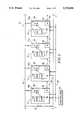
- FIG. 3is a block diagram of a single processor node of the invention.
- FIG. 1an array of single instruction stream, multiple data stream (SIMD) processor nodes are shown generally at 10.
- Array 10includes processor nodes 12, 14, 16 and 18, and may contain as many more processor nodes as are desired for a particular application.
- FIG. 1contains only four such processor nodes for the sake of brevity and to allow an explanation of the interaction between multiple processor nodes.
- Each processor nodeis connected to an input bus 20 and an output bus 22.
- Buses 20 and 22are depicted as being single entity structures in FIG. 1, however, in some circumstances, both the input and/or output bus may be multiple bus structures.
- a single controller 24is connected to a control bus 26, which in turn is connected to each of the processor nodes.
- output bus 22may be connected directly to input bus 20 by means of a connection 28, or, output bus 22 may be connected to the input bus of another array of processor nodes, while the output bus of another array of processor nodes may be connected to input bus 20.
- each processor nodeincludes a pair, or more, of communication nodes, such as the connection node (CN) depicted at 30-37 in processor nodes 12-18.
- a CNis a state associated with an emulated node in a neural network located in a PN.
- Each PNmay have several CNs located therein.
- processor node 12contains the state information for connection node .0.
- processor node 14contains the state information for connection node 1 (CN1) and the state information for connection node 5 (CN5)
- processor node 16contains the state information for connection node 2 (CN2) and the state information for connection node 6 (CN6)
- processor node 18contains the state information for connection node 3 (CN3) and the state information for connection node 7 (CN7).
- connection nodes .0.-7are depicted.
- the CNsare arranged in "layers", with CN.0.-CN3 comprising one layer, while CN4-CN7 comprise a second layer.
- the connection nodesoperate in what is referred to as a broadcast hierarchy, wherein each of connection nodes .0.-3 broadcast to each of connection nodes 4-7.
- An illustrative technique for arranging such a broadcast hierarchyis disclosed in U.S. Pat. No. 4,796,199, NEURAL-MODEL INFORMATION-HANDLING ARCHITECTURE AND METHOD, to Hammerstrom et al, Jan. 3, 1989, which is incorporated herein by reference.
- the available processor nodesmay be thought of as a "layer" of processors, each executing its function (multiply, accumulate, and increment weight index) for each input, on each clock, wherein one processor node broadcasts its output to all other processor nodes.
- the output processor node arrangementit is possible to provide n 2 connections in n clocks using only a two layer arrangement.
- conventional SIMD structuresmay accomplish n 2 connections in n clocks, but require a three layer configuration, or 50% more structure.
- a normal sequence of events in the SIMD array depicted at 10begins with a specific piece of data being transmitted to each processor node. The data is acted upon by an instruction which is transmitted over input bus 20. Each processor node performs whatever operation is required on the data, and then attempts to transmit the information on output bus 22. Obviously, not every processor node can transmit on the output bus simultaneously, and under normal conditions, the processor nodes have to wait for a number of clocks, or cycles, until each processor node in the array has transmitted its information on the output bus.
- output processorsor output buffers, such as those depicted at 38, 40, 42 and 44 are included in the architecture of each processor node.
- the output buffersreceive the information from an associated connection node and hold the information or data until such time as each processor node receives clearance to transmit on output bus 22. Because the data is held in the output buffer, the remainder of the processor node can perform other functions while the output processor node is waiting to transmit.
- each processor nodecontains a flip flop, such as flip flops 46, 48, 50 and 52.
- Flip flopsare also referred to herein as arbitration signal generators.
- Node 12includes an input unit 54 which is connected to input bus 20 and output bus 30. Again, only single input and output buses are depicted for the sake of simplicity. Where multiple input and/or output buses are provided, input unit 54, and the other units which will be described herein, have connections to each input and output bus.
- a processor node controller 56is provided to establish operational parameters for each processor node.
- An addition unit 58provides addition operations and receives input from input unit 54, a multiplier 60, and is connected to the input and output buses.
- a register unit 62contains an array of registers, which in the preferred embodiment of the architecture includes an array of 32 16-bit registers. A number of other arrangements may be utilized.
- a weight address generation unit 64computes the next address for a weight memory unit 66. In the preferred embodiment, the memory address may be set in one of two ways: (1) by a direct write to a weight address register, or (2) by asserting a command which causes the contents of a weight offset register to be added to the current contents of the memory address register, thereby producing a new address.
- Node controller 56, addition unit 58, multiplier unit 60 register unit 62 and weight address generation unit 64comprise what is referred to herein as a manipulation unit.
- An output unit 68is provided to store data prior to the data of being transmitted on output bus 22.
- Output unit 68includes output processor node, 38, which receives data from the remainder of the output unit prior to the data being transmitted. Data is transmitted to output bus 22 by means of one or more connection nodes, such as connection node 30 or 34, which are part of the output unit.
- Output unit 68includes an output buffer register which initially receives processed data. Once this data is loaded into the register, the output buffer unit becomes "armed”. Once armed, the output buffer operates independently, but synchronously, from the rest of the processing node.
- An arbitration processis provided between the output buffers of the different processor nodes in order to determine which output buffer, or output processor node, will transmit first over output bus 22, since only one PN can use the output bus at any one time.
- a hand shake arrangementextending from a flip flop, such as flip flop 46 in processor node 12, and indicated by arrow 70, signals the next processor node to transmit.
- FIG. 1indicates that the transmission occurs from immediately adjacent nodes, this is not necessarily representative of what may happen in the actual processor node array. It may be that some other order of transmission is determined by the arbitration process.
- Arbitration and transmissionoccur only when a transmit signal is asserted by controller 24 to allow synchronization of the transmission with other operations being conducted in the array.
- Several modes of arbitration/data transferare provided in the architecture: sequential, global and direct.
- the arbitration modeis selected by controller 24.
- Controller 24 and flip flops 46, 48, 50 and 52comprise what is referred to herein as arbitration means, which is operable to determine at which point in processor operation a signal will be transmitted from a output processor node.
- Sequential moderequires a control signal over control bus 26 to travel from one processor node to the next.
- Global arbitrationuses a signal that travels on the control bus which enables transmission from all processor nodes, but which operates the processor nodes in a daisy-chain, allowing certain processor nodes to transmit while others may pass, i.e., thereby not transmitting any data for a particular cycle, or clock.
- Direct arbitrationis used in a situation where data is written directly into the output buffer and immediately transmitted over the output bus on the next transmit cycle.
- a single instructionpasses over control bus 26 to all of the processor nodes.
- the instructionis carried out, simultaneously, on the values which are present in the individual processor nodes, which have been input over input bus 20.
- Each output bufferhas its own internal controller, depicted in FIG. 1 at 38a, 40a, 42a and 44a, which is described in the code and structure which follow herein, which is how each output processor operates separately from SIMD control 24.
- the outputis transmitted over output bus 22 in a predetermined sequencing of transmissions from the individual processor nodes. This of course, requires that the processor node wait until the other processor nodes in the array are finished transmitting before a new instruction set or new data can be received in the processor node.
- the provision of output buffers in each PNprovides a location where the process data may be stored while the processor node waits its turn at the output bus. Additional operations may be occurring in the processor nodes, which may have new data loaded, or which may have existing data acted upon by a new instruction set.
- Connection 28may be enabled if it is desired that the output data from a processor node become the input data for a processor node, or other processor nodes. Such enablement is accomplished by conventional micro-circuitry mechanisms, and is depicted schematically in FIG. 2.
- the following codeis a simplification of the code that describes the actual CMOS implementation of the PN structure in a neurocomputer chip.
- the code shown belowis in the C programming language embellished by certain predefined macros.
- the codeis used as a register transfer level description language in the actual implementation of the circuitry described here.
- Bolded textindicates a signal, hardware or firmware component, or a phase or clock cycle.
- the ph1 and ph2 variablessimulate the two phases in the two-phase, non-overlapping clock used to implement dynamic MOS devices.
- -- Dmeans a delayed version of the signal
- -- Bmeans a bus (more than one signal line)
- -- 1means a dynamic signal that is only valid during ph1.
- Output unit (obUNIT) 68contains the output buffer.
- the PN Output Buffer Interfaceis used for output and allows the output to run independently from the input, and is used during various recursive and feedback operations. ##EQU1## This step initialize variables which are used during the processing.
- the arbitration signal from a PN's left most neighborwill set the sequential arbitration ok signal, seqgo -- 1D.
- leftffis the signal from flip flop 46, also referred to herein as arbitration signal generator means, in PN 12, on the left and indicates that PN 12 has transmitted and it is now PN 14's turn.
- the obarmd flip flop 46When the output buffer is written, the obarmd flip flop 46 is set. obarmd indicates that the output buffer is armed and ready to transmit. This transmission operates independently of the remaining computation inside the PN and forms the essence of the output buffer architecture of the invention.
- the low byteis sent first. This occurs if the transmit control is asserted and if the PN's output buffer is armed.
- the outst flip flopis used to indicate that this is the second of a two byte transmission. All of the arbitration decisions discussed at this point operate in the sequential mode, where a PN signals its neighbor to the right when it has completed its transmission. xmit is the SIMD command that tells the output buffer of a particular PN to transmit (if it has received an arbitration signal).
- the seqarb flip flopindicates that this arbitration mode is enabled.
- outmd2indicates that this is a two byte transmission: ##EQU2##
- the previous sequenceexecutes the outbuf state machine for sequential arbitration. seqrght signals the next PN to transmit on the next clock ##EQU3##
- obarmdis set and the cycle repeats.
- vcvalindicates a valid output buffer control signal
- rgctl -- B2indicates that a write to the output buffer is now occurring
- r -- Bindicates the output buffer, F -- OUTBUF, is being addressed.
- Writing to the register OUTBUFsets obarmd, which turns on (enables) the PN output buffer.
- CN.0., CN1, CN2 and CN3have values which are located in register 62 of processor nodes 12, 14, 16 and 18, respectively. The values are written to the respective output buffer in each PN over an appropriate connection.
- Output buffer 38 in processor node 12transmits the output of CN.0. onto output bus 22. This value is read by processor nodes 12, 14, 16 and 18 over connection 28 and input bus 20. Each processor node fetches a weight from weight memory 66 and multiplies, for instance, the output of CN.0. times the various weights, such as w 4 .0., w 5 .0., w 6 .0. and w 7 .0.. Output buffer 38 and processor node 12 then transmit an arbitration signal, through flip flop 47 and connection 70, to output buffer 40 in processor node 14, the next-in-time processor node, that it may now transmit on output bus 22.
- Output buffer 40 in processor node 14transmits the output of CN1 onto output bus 22. This value is read by processor nodes 12, 14, 16 and 18 over connection 28 and input bus 20. Each processor node fetches a weight from weight memory 66 and multiplies, for instance, the output of CN.0. times the various weights, such as w 41 , w 51 , w 61 and w 71 . Output buffer 40 and processor node 14 then signal, by flip flop 48 and connection 70, output buffer 42 in processor node 16 that it may now transmit. Similar action occurs during successive clock cycles until the data has been processed.
- each processor nodehas a multiplier 60, an adder 58 and two look tables, weight address generation 64 and weight memory 66.
- Each nodereceives an input and does a multiply-accumulate on each clock. After the accumulation loop, each processor node moves its output into its output buffer and waits for its turn to broadcast.
- the stepsmay be represented as ##EQU5##
- the output, O iis therefore equal to the summation of the values drawn from weight memory 66, W ij , times the input value, O j , wherein the entire function is stored in the weight address generator 64.
- Processors constructed according to the inventionare useful in neural network systems which may be used to simulate human brain functions in analysis and decision making applications.
Landscapes
- Engineering & Computer Science (AREA)
- Computer Hardware Design (AREA)
- Physics & Mathematics (AREA)
- Theoretical Computer Science (AREA)
- Mathematical Physics (AREA)
- Software Systems (AREA)
- General Engineering & Computer Science (AREA)
- General Physics & Mathematics (AREA)
- Multi Processors (AREA)
Abstract
Description
if (ph1) seqgo.sub.-- 1D=leftff;
Claims (10)
Priority Applications (1)
| Application Number | Priority Date | Filing Date | Title |
|---|---|---|---|
| US07/664,087US5175858A (en) | 1991-03-04 | 1991-03-04 | Mechanism providing concurrent computational/communications in SIMD architecture |
Applications Claiming Priority (1)
| Application Number | Priority Date | Filing Date | Title |
|---|---|---|---|
| US07/664,087US5175858A (en) | 1991-03-04 | 1991-03-04 | Mechanism providing concurrent computational/communications in SIMD architecture |
Publications (1)
| Publication Number | Publication Date |
|---|---|
| US5175858Atrue US5175858A (en) | 1992-12-29 |
Family
ID=24664463
Family Applications (1)
| Application Number | Title | Priority Date | Filing Date |
|---|---|---|---|
| US07/664,087Expired - LifetimeUS5175858A (en) | 1991-03-04 | 1991-03-04 | Mechanism providing concurrent computational/communications in SIMD architecture |
Country Status (1)
| Country | Link |
|---|---|
| US (1) | US5175858A (en) |
Cited By (29)
| Publication number | Priority date | Publication date | Assignee | Title |
|---|---|---|---|---|
| US5479574A (en)* | 1993-04-01 | 1995-12-26 | Nestor, Inc. | Method and apparatus for adaptive classification |
| US5498947A (en)* | 1994-05-05 | 1996-03-12 | Fortis Co. | Frequency and amplitude variable waveform synthesizer |
| US5511212A (en)* | 1993-06-10 | 1996-04-23 | Rockoff; Todd E. | Multi-clock SIMD computer and instruction-cache-enhancement thereof |
| US5532938A (en)* | 1994-01-28 | 1996-07-02 | Mitsubishi Denki Kabushiki Kaisha | Numerical arithmetic processing unit |
| US5537562A (en)* | 1993-03-31 | 1996-07-16 | Motorola Inc. | Data processing system and method thereof |
| US5548771A (en)* | 1993-11-02 | 1996-08-20 | Motorola Inc. | Multi-processor data processing system having multiple ports coupled to multiple interface circuits |
| US5603046A (en)* | 1993-11-02 | 1997-02-11 | Motorola Inc. | Method for complex data movement in a multi-processor data processing system |
| US5872988A (en)* | 1992-06-17 | 1999-02-16 | U.S. Philips Corporation | Parallel data processing device having a concatenated data path between elementary processors |
| GB2348977A (en)* | 1999-04-09 | 2000-10-18 | Pixelfusion Ltd | Parallel data processing systems with a SIMD array |
| GB2352306A (en)* | 1999-04-09 | 2001-01-24 | Pixelfusion Ltd | Parallel processing apparatus using a SIMD array |
| US6199057B1 (en) | 1996-10-23 | 2001-03-06 | California Institute Of Technology | Bit-serial neuroprocessor architecture |
| US20010043612A1 (en)* | 2000-05-18 | 2001-11-22 | Johnson Ian David | Apparatus and method for resource arbitration |
| US20040252547A1 (en)* | 2003-06-06 | 2004-12-16 | Chengpu Wang | Concurrent Processing Memory |
| US20070226458A1 (en)* | 1999-04-09 | 2007-09-27 | Dave Stuttard | Parallel data processing apparatus |
| US20070245132A1 (en)* | 1999-04-09 | 2007-10-18 | Dave Stuttard | Parallel data processing apparatus |
| US20070245123A1 (en)* | 1999-04-09 | 2007-10-18 | Dave Stuttard | Parallel data processing apparatus |
| US20070294510A1 (en)* | 1999-04-09 | 2007-12-20 | Dave Stuttard | Parallel data processing apparatus |
| US20080008393A1 (en)* | 1999-04-09 | 2008-01-10 | Dave Stuttard | Parallel data processing apparatus |
| US20080007562A1 (en)* | 1999-04-09 | 2008-01-10 | Dave Stuttard | Parallel data processing apparatus |
| US20080016318A1 (en)* | 1999-04-09 | 2008-01-17 | Dave Stuttard | Parallel data processing apparatus |
| US20080028184A1 (en)* | 1999-04-09 | 2008-01-31 | Dave Stuttard | Parallel data processing apparatus |
| US20080034186A1 (en)* | 1999-04-09 | 2008-02-07 | Dave Stuttard | Parallel data processing apparatus |
| US20080052492A1 (en)* | 1999-04-09 | 2008-02-28 | Dave Stuttard | Parallel data processing apparatus |
| US20080098201A1 (en)* | 1999-04-09 | 2008-04-24 | Dave Stuttard | Parallel data processing apparatus |
| US20080184017A1 (en)* | 1999-04-09 | 2008-07-31 | Dave Stuttard | Parallel data processing apparatus |
| US7924274B2 (en) | 2003-05-20 | 2011-04-12 | Syndiant, Inc. | Masked write on an array of drive bits |
| US7966475B2 (en) | 1999-04-09 | 2011-06-21 | Rambus Inc. | Parallel data processing apparatus |
| US8171263B2 (en) | 1999-04-09 | 2012-05-01 | Rambus Inc. | Data processing apparatus comprising an array controller for separating an instruction stream processing instructions and data transfer instructions |
| US8174530B2 (en) | 1999-04-09 | 2012-05-08 | Rambus Inc. | Parallel date processing apparatus |
Citations (20)
| Publication number | Priority date | Publication date | Assignee | Title |
|---|---|---|---|---|
| US4380046A (en)* | 1979-05-21 | 1983-04-12 | Nasa | Massively parallel processor computer |
| US4384273A (en)* | 1981-03-20 | 1983-05-17 | Bell Telephone Laboratories, Incorporated | Time warp signal recognition processor for matching signal patterns |
| US4412303A (en)* | 1979-11-26 | 1983-10-25 | Burroughs Corporation | Array processor architecture |
| US4481580A (en)* | 1979-11-19 | 1984-11-06 | Sperry Corporation | Distributed data transfer control for parallel processor architectures |
| US4498134A (en)* | 1982-01-26 | 1985-02-05 | Hughes Aircraft Company | Segregator functional plane for use in a modular array processor |
| US4574394A (en)* | 1981-06-01 | 1986-03-04 | Environmental Research Institute Of Mi | Pipeline processor |
| US4580215A (en)* | 1983-03-08 | 1986-04-01 | Itt Corporation | Associative array with five arithmetic paths |
| US4591981A (en)* | 1982-04-26 | 1986-05-27 | V M E I "Lenin" Quartal Darvenitza | Multimicroprocessor system |
| US4593351A (en)* | 1981-06-12 | 1986-06-03 | International Business Machines Corporation | High speed machine for the physical design of very large scale integrated circuits |
| US4592933A (en)* | 1984-06-29 | 1986-06-03 | International Business Machines Corporation | High efficiency homogeneous chemical vapor deposition |
| US4621339A (en)* | 1983-06-13 | 1986-11-04 | Duke University | SIMD machine using cube connected cycles network architecture for vector processing |
| US4720780A (en)* | 1985-09-17 | 1988-01-19 | The Johns Hopkins University | Memory-linked wavefront array processor |
| US4773038A (en)* | 1986-02-24 | 1988-09-20 | Thinking Machines Corporation | Method of simulating additional processors in a SIMD parallel processor array |
| US4792894A (en)* | 1987-03-17 | 1988-12-20 | Unisys Corporation | Arithmetic computation modifier based upon data dependent operations for SIMD architectures |
| US4823281A (en)* | 1985-04-30 | 1989-04-18 | Ibm Corporation | Color graphic processor for performing logical operations |
| US4852048A (en)* | 1985-12-12 | 1989-07-25 | Itt Corporation | Single instruction multiple data (SIMD) cellular array processing apparatus employing a common bus where a first number of bits manifest a first bus portion and a second number of bits manifest a second bus portion |
| US4855903A (en)* | 1984-12-20 | 1989-08-08 | State University Of New York | Topologically-distributed-memory multiprocessor computer |
| US4873626A (en)* | 1986-12-17 | 1989-10-10 | Massachusetts Institute Of Technology | Parallel processing system with processor array having memory system included in system memory |
| US4945479A (en)* | 1985-07-31 | 1990-07-31 | Unisys Corporation | Tightly coupled scientific processing system |
| US5072371A (en)* | 1989-03-01 | 1991-12-10 | The United States Of America As Represented By The United States Department Of Energy | Method for simultaneous overlapped communications between neighboring processors in a multiple |
- 1991
- 1991-03-04USUS07/664,087patent/US5175858A/ennot_activeExpired - Lifetime
Patent Citations (20)
| Publication number | Priority date | Publication date | Assignee | Title |
|---|---|---|---|---|
| US4380046A (en)* | 1979-05-21 | 1983-04-12 | Nasa | Massively parallel processor computer |
| US4481580A (en)* | 1979-11-19 | 1984-11-06 | Sperry Corporation | Distributed data transfer control for parallel processor architectures |
| US4412303A (en)* | 1979-11-26 | 1983-10-25 | Burroughs Corporation | Array processor architecture |
| US4384273A (en)* | 1981-03-20 | 1983-05-17 | Bell Telephone Laboratories, Incorporated | Time warp signal recognition processor for matching signal patterns |
| US4574394A (en)* | 1981-06-01 | 1986-03-04 | Environmental Research Institute Of Mi | Pipeline processor |
| US4593351A (en)* | 1981-06-12 | 1986-06-03 | International Business Machines Corporation | High speed machine for the physical design of very large scale integrated circuits |
| US4498134A (en)* | 1982-01-26 | 1985-02-05 | Hughes Aircraft Company | Segregator functional plane for use in a modular array processor |
| US4591981A (en)* | 1982-04-26 | 1986-05-27 | V M E I "Lenin" Quartal Darvenitza | Multimicroprocessor system |
| US4580215A (en)* | 1983-03-08 | 1986-04-01 | Itt Corporation | Associative array with five arithmetic paths |
| US4621339A (en)* | 1983-06-13 | 1986-11-04 | Duke University | SIMD machine using cube connected cycles network architecture for vector processing |
| US4592933A (en)* | 1984-06-29 | 1986-06-03 | International Business Machines Corporation | High efficiency homogeneous chemical vapor deposition |
| US4855903A (en)* | 1984-12-20 | 1989-08-08 | State University Of New York | Topologically-distributed-memory multiprocessor computer |
| US4823281A (en)* | 1985-04-30 | 1989-04-18 | Ibm Corporation | Color graphic processor for performing logical operations |
| US4945479A (en)* | 1985-07-31 | 1990-07-31 | Unisys Corporation | Tightly coupled scientific processing system |
| US4720780A (en)* | 1985-09-17 | 1988-01-19 | The Johns Hopkins University | Memory-linked wavefront array processor |
| US4852048A (en)* | 1985-12-12 | 1989-07-25 | Itt Corporation | Single instruction multiple data (SIMD) cellular array processing apparatus employing a common bus where a first number of bits manifest a first bus portion and a second number of bits manifest a second bus portion |
| US4773038A (en)* | 1986-02-24 | 1988-09-20 | Thinking Machines Corporation | Method of simulating additional processors in a SIMD parallel processor array |
| US4873626A (en)* | 1986-12-17 | 1989-10-10 | Massachusetts Institute Of Technology | Parallel processing system with processor array having memory system included in system memory |
| US4792894A (en)* | 1987-03-17 | 1988-12-20 | Unisys Corporation | Arithmetic computation modifier based upon data dependent operations for SIMD architectures |
| US5072371A (en)* | 1989-03-01 | 1991-12-10 | The United States Of America As Represented By The United States Department Of Energy | Method for simultaneous overlapped communications between neighboring processors in a multiple |
Cited By (65)
| Publication number | Priority date | Publication date | Assignee | Title |
|---|---|---|---|---|
| US5872988A (en)* | 1992-06-17 | 1999-02-16 | U.S. Philips Corporation | Parallel data processing device having a concatenated data path between elementary processors |
| US5737586A (en)* | 1993-03-31 | 1998-04-07 | Motorola, Inc. | Data processing system and method thereof |
| US5805874A (en)* | 1993-03-31 | 1998-09-08 | Motorola Inc. | Method and apparatus for performing a vector skip instruction in a data processor |
| US6085275A (en)* | 1993-03-31 | 2000-07-04 | Motorola, Inc. | Data processing system and method thereof |
| US5537562A (en)* | 1993-03-31 | 1996-07-16 | Motorola Inc. | Data processing system and method thereof |
| US5706488A (en)* | 1993-03-31 | 1998-01-06 | Motorola, Inc. | Data processing system and method thereof |
| US5548768A (en)* | 1993-03-31 | 1996-08-20 | Motorola, Inc. | Data processing system and method thereof |
| US5559973A (en)* | 1993-03-31 | 1996-09-24 | Motorola Inc. | Data processing system and method thereof |
| US5572689A (en)* | 1993-03-31 | 1996-11-05 | Motorola, Inc. | Data processing system and method thereof |
| US5598571A (en)* | 1993-03-31 | 1997-01-28 | Motorola Inc. | Data processor for conditionally modifying extension bits in response to data processing instruction execution |
| US5600811A (en)* | 1993-03-31 | 1997-02-04 | Motorola Inc. | Vector move instruction in a vector data processing system and method therefor |
| US5600846A (en)* | 1993-03-31 | 1997-02-04 | Motorola Inc. | Data processing system and method thereof |
| US5790854A (en)* | 1993-03-31 | 1998-08-04 | Motorola Inc. | Efficient stack utilization for compiling and executing nested if-else constructs in a vector data processing system |
| US5754805A (en)* | 1993-03-31 | 1998-05-19 | Motorola Inc. | Instruction in a data processing system utilizing extension bits and method therefor |
| US5664134A (en)* | 1993-03-31 | 1997-09-02 | Motorola Inc. | Data processor for performing a comparison instruction using selective enablement and wired boolean logic |
| US5742786A (en)* | 1993-03-31 | 1998-04-21 | Motorola, Inc. | Method and apparatus for storing vector data in multiple non-consecutive locations in a data processor using a mask value |
| US5717947A (en)* | 1993-03-31 | 1998-02-10 | Motorola, Inc. | Data processing system and method thereof |
| US5734879A (en)* | 1993-03-31 | 1998-03-31 | Motorola, Inc. | Saturation instruction in a data processor |
| US5752074A (en)* | 1993-03-31 | 1998-05-12 | Motorola, Inc. | Data processing system and method thereof |
| US5479574A (en)* | 1993-04-01 | 1995-12-26 | Nestor, Inc. | Method and apparatus for adaptive classification |
| US5511212A (en)* | 1993-06-10 | 1996-04-23 | Rockoff; Todd E. | Multi-clock SIMD computer and instruction-cache-enhancement thereof |
| US5708839A (en)* | 1993-11-02 | 1998-01-13 | Motorola, Inc. | Method and apparatus for providing bus protocol simulation |
| US5603046A (en)* | 1993-11-02 | 1997-02-11 | Motorola Inc. | Method for complex data movement in a multi-processor data processing system |
| US5548771A (en)* | 1993-11-02 | 1996-08-20 | Motorola Inc. | Multi-processor data processing system having multiple ports coupled to multiple interface circuits |
| US5532938A (en)* | 1994-01-28 | 1996-07-02 | Mitsubishi Denki Kabushiki Kaisha | Numerical arithmetic processing unit |
| US5498947A (en)* | 1994-05-05 | 1996-03-12 | Fortis Co. | Frequency and amplitude variable waveform synthesizer |
| US6199057B1 (en) | 1996-10-23 | 2001-03-06 | California Institute Of Technology | Bit-serial neuroprocessor architecture |
| US20070245132A1 (en)* | 1999-04-09 | 2007-10-18 | Dave Stuttard | Parallel data processing apparatus |
| US7526630B2 (en) | 1999-04-09 | 2009-04-28 | Clearspeed Technology, Plc | Parallel data processing apparatus |
| US8762691B2 (en) | 1999-04-09 | 2014-06-24 | Rambus Inc. | Memory access consolidation for SIMD processing elements using transaction identifiers |
| US8174530B2 (en) | 1999-04-09 | 2012-05-08 | Rambus Inc. | Parallel date processing apparatus |
| US8169440B2 (en) | 1999-04-09 | 2012-05-01 | Rambus Inc. | Parallel data processing apparatus |
| US20070226458A1 (en)* | 1999-04-09 | 2007-09-27 | Dave Stuttard | Parallel data processing apparatus |
| GB2348977A (en)* | 1999-04-09 | 2000-10-18 | Pixelfusion Ltd | Parallel data processing systems with a SIMD array |
| US20070245123A1 (en)* | 1999-04-09 | 2007-10-18 | Dave Stuttard | Parallel data processing apparatus |
| US20070294510A1 (en)* | 1999-04-09 | 2007-12-20 | Dave Stuttard | Parallel data processing apparatus |
| US20080008393A1 (en)* | 1999-04-09 | 2008-01-10 | Dave Stuttard | Parallel data processing apparatus |
| US20080007562A1 (en)* | 1999-04-09 | 2008-01-10 | Dave Stuttard | Parallel data processing apparatus |
| US20080016318A1 (en)* | 1999-04-09 | 2008-01-17 | Dave Stuttard | Parallel data processing apparatus |
| US20080028184A1 (en)* | 1999-04-09 | 2008-01-31 | Dave Stuttard | Parallel data processing apparatus |
| US20080034186A1 (en)* | 1999-04-09 | 2008-02-07 | Dave Stuttard | Parallel data processing apparatus |
| US20080040575A1 (en)* | 1999-04-09 | 2008-02-14 | Dave Stuttard | Parallel data processing apparatus |
| US20080052492A1 (en)* | 1999-04-09 | 2008-02-28 | Dave Stuttard | Parallel data processing apparatus |
| US20080098201A1 (en)* | 1999-04-09 | 2008-04-24 | Dave Stuttard | Parallel data processing apparatus |
| US20080184017A1 (en)* | 1999-04-09 | 2008-07-31 | Dave Stuttard | Parallel data processing apparatus |
| US7506136B2 (en) | 1999-04-09 | 2009-03-17 | Clearspeed Technology Plc | Parallel data processing apparatus |
| GB2352306A (en)* | 1999-04-09 | 2001-01-24 | Pixelfusion Ltd | Parallel processing apparatus using a SIMD array |
| US20090198898A1 (en)* | 1999-04-09 | 2009-08-06 | Clearspeed Technology Plc | Parallel data processing apparatus |
| US7627736B2 (en) | 1999-04-09 | 2009-12-01 | Clearspeed Technology Plc | Thread manager to control an array of processing elements |
| US7802079B2 (en) | 1999-04-09 | 2010-09-21 | Clearspeed Technology Limited | Parallel data processing apparatus |
| US8171263B2 (en) | 1999-04-09 | 2012-05-01 | Rambus Inc. | Data processing apparatus comprising an array controller for separating an instruction stream processing instructions and data transfer instructions |
| US7925861B2 (en) | 1999-04-09 | 2011-04-12 | Rambus Inc. | Plural SIMD arrays processing threads fetched in parallel and prioritized by thread manager sequentially transferring instructions to array controller for distribution |
| US7958332B2 (en) | 1999-04-09 | 2011-06-07 | Rambus Inc. | Parallel data processing apparatus |
| US7966475B2 (en) | 1999-04-09 | 2011-06-21 | Rambus Inc. | Parallel data processing apparatus |
| US6937133B2 (en)* | 2000-05-18 | 2005-08-30 | Xyratex Technology Limited | Apparatus and method for resource arbitration |
| US20010043612A1 (en)* | 2000-05-18 | 2001-11-22 | Johnson Ian David | Apparatus and method for resource arbitration |
| US8004505B2 (en) | 2003-05-20 | 2011-08-23 | Syndiant Inc. | Variable storage of bits on a backplane |
| US8035627B2 (en) | 2003-05-20 | 2011-10-11 | Syndiant Inc. | Bit serial control of light modulating elements |
| US8089431B2 (en)* | 2003-05-20 | 2012-01-03 | Syndiant, Inc. | Instructions controlling light modulating elements |
| US8120597B2 (en) | 2003-05-20 | 2012-02-21 | Syndiant Inc. | Mapping pixel values |
| US7924274B2 (en) | 2003-05-20 | 2011-04-12 | Syndiant, Inc. | Masked write on an array of drive bits |
| US8189015B2 (en) | 2003-05-20 | 2012-05-29 | Syndiant, Inc. | Allocating memory on a spatial light modulator |
| US8558856B2 (en) | 2003-05-20 | 2013-10-15 | Syndiant, Inc. | Allocation registers on a spatial light modulator |
| US8766887B2 (en) | 2003-05-20 | 2014-07-01 | Syndiant, Inc. | Allocating registers on a spatial light modulator |
| US20040252547A1 (en)* | 2003-06-06 | 2004-12-16 | Chengpu Wang | Concurrent Processing Memory |
Similar Documents
| Publication | Publication Date | Title |
|---|---|---|
| US5175858A (en) | Mechanism providing concurrent computational/communications in SIMD architecture | |
| US5369773A (en) | Neural network using virtual-zero | |
| JáJá | Parallel algorithms | |
| Uhr | Algorithm-structured computer arrays and networks: architectures and processes for images, percepts, models, information | |
| US5204938A (en) | Method of implementing a neural network on a digital computer | |
| US5325510A (en) | Multiprocessor system and architecture with a computation system for minimizing duplicate read requests | |
| Ramacher | SYNAPSE—A neurocomputer that synthesizes neural algorithms on a parallel systolic engine | |
| US5600843A (en) | Ring systolic array system for synchronously performing matrix/neuron computation using data transferred through cyclic shift register connected in cascade of trays | |
| US11782760B2 (en) | Time-multiplexed use of reconfigurable hardware | |
| US12333351B2 (en) | Synchronization of processing elements that execute statically scheduled instructions in a machine learning accelerator | |
| WO1993014459A1 (en) | Modular parallel processing system | |
| US5586289A (en) | Method and apparatus for accessing local storage within a parallel processing computer | |
| JPH05108341A (en) | Micro Processor | |
| WO1991019256A1 (en) | Mechanism providing concurrent computational/communications in simd architecture | |
| EP0223849B1 (en) | Super-computer system architectures | |
| EP0834817B1 (en) | Programmed neural module | |
| Kerckhoffs et al. | Speeding up backpropagation training on a hypercube computer | |
| Nordström | Highly parallel computers for artificial neural networks | |
| US5855010A (en) | Data processing apparatus | |
| Abdallah et al. | Comprehensive Review of Neuromorphic Systems | |
| Wilson | Neural Computing on a One Dimensional SIMD Array. | |
| CN111767133A (en) | System and method for reconfigurable systolic array | |
| Molendijk et al. | Benchmarking the epiphany processor as a reference neuromorphic architecture | |
| Hoshino et al. | Transputer network for dynamic control of multiple manipulators | |
| Svensson et al. | Towards modular, massively parallel neural computers |
Legal Events
| Date | Code | Title | Description |
|---|---|---|---|
| AS | Assignment | Owner name:ADAPTIVE SOLUTIONS, INC., BEAVERTON, COUNTY OF WAS Free format text:ASSIGNMENT OF ASSIGNORS INTEREST.;ASSIGNOR:HAMMERSTROM, DANIEL W.;REEL/FRAME:005638/0871 Effective date:19910227 | |
| STCF | Information on status: patent grant | Free format text:PATENTED CASE | |
| FPAY | Fee payment | Year of fee payment:4 | |
| FPAY | Fee payment | Year of fee payment:8 | |
| AS | Assignment | Owner name:EISTREAM TECHNOLOGIES, INC., TEXAS Free format text:ASSIGNMENT OF ASSIGNORS INTEREST;ASSIGNOR:KOFILE, INC.;REEL/FRAME:013221/0367 Effective date:20020814 | |
| FEPP | Fee payment procedure | Free format text:PAYOR NUMBER ASSIGNED (ORIGINAL EVENT CODE: ASPN); ENTITY STATUS OF PATENT OWNER: SMALL ENTITY | |
| FPAY | Fee payment | Year of fee payment:12 | |
| AS | Assignment | Owner name:GLOBAL 360, INC., TEXAS Free format text:MERGER;ASSIGNORS:EISTREAM WMS, INC.;EISTREAM VIEWSTAR, INC.;EISTREAM GOVERNMENT SOLUTIONS, INC.;AND OTHERS;REEL/FRAME:016369/0636 Effective date:20041215 Owner name:GLOBAL 360, INC., TEXAS Free format text:MERGER;ASSIGNORS:EISTREAM WMS, INC.;EISTREAM VIEWSTAR, INC.;EISTREAM GOVERNMENT SOLUTIONS, INC.;AND OTHERS;REEL/FRAME:016369/0649 Effective date:20041215 | |
| AS | Assignment | Owner name:KOFILE, INC., NEW YORK Free format text:BILL OF SALE;ASSIGNOR:ADAPTIVE SOLUTIONS, INC.;REEL/FRAME:017344/0084 Effective date:19990113 | |
| AS | Assignment | Owner name:WELLS FARGO FOOTHILL, INC., AS AGENT, CALIFORNIA Free format text:SECURITY AGREEMENT;ASSIGNORS:GLOBAL 360, INC.;GLOBAL 360 BGS, INC.;REEL/FRAME:017448/0474 Effective date:20060331 | |
| AS | Assignment | Owner name:GLOBAL 360 BGS, INC., TEXAS Free format text:RELEASE BY SECURED PARTY;ASSIGNOR:WELLS FARGO CAPITAL FINANCE, INC. (F/K/A WELLS FARGO FOOTHILL, INC.);REEL/FRAME:027028/0271 Effective date:20110713 Owner name:GLOBAL 360, INC., TEXAS Free format text:RELEASE BY SECURED PARTY;ASSIGNOR:WELLS FARGO CAPITAL FINANCE, INC. (F/K/A WELLS FARGO FOOTHILL, INC.);REEL/FRAME:027028/0271 Effective date:20110713 |