US5175560A - Notch radiator elements - Google Patents
Notch radiator elementsDownload PDFInfo
- Publication number
- US5175560A US5175560AUS07/674,003US67400391AUS5175560AUS 5175560 AUS5175560 AUS 5175560AUS 67400391 AUS67400391 AUS 67400391AUS 5175560 AUS5175560 AUS 5175560A
- Authority
- US
- United States
- Prior art keywords
- conductive strip
- aperture
- radiator element
- substrate
- slot line
- Prior art date
- Legal status (The legal status is an assumption and is not a legal conclusion. Google has not performed a legal analysis and makes no representation as to the accuracy of the status listed.)
- Expired - Lifetime
Links
Images


Classifications
- H—ELECTRICITY
- H01—ELECTRIC ELEMENTS
- H01Q—ANTENNAS, i.e. RADIO AERIALS
- H01Q13/00—Waveguide horns or mouths; Slot antennas; Leaky-waveguide antennas; Equivalent structures causing radiation along the transmission path of a guided wave
- H01Q13/08—Radiating ends of two-conductor microwave transmission lines, e.g. of coaxial lines, of microstrip lines
- H01Q13/085—Slot-line radiating ends
Definitions
- the inventionrelates to notch radiator elements.
- the inventionrelates to high frequency notch radiator devices employing circuit elements in printed and machined arrangements for use in antenna arrays.
- Known notch type radiator elementssuch as element 10 in FIG. 1 comprise a 50 ohm stripline 12 and a notch antenna 14.
- a double slot line tapered launch or aperture 16has a narrow 50 ohm feed end 18 fed by the stripline 12 and a wide 376 ohm radiating aperture 20 which matches the air.
- the stripline 12 and the feed end 18have respective quarter wavelength extensions 22 and 24 which form terminations for each.
- the stripline 12is buried within a dielectric substrate 26 and the aperture 16 is formed of etched metallized films on opposite sides of the substrate 26.
- the radiator 10is designed to transmit or receive RF signals.
- a signal carried by the stripline 12sets up an electric field in the feed end 18 of the aperture 16.
- the electric fieldradiates outwardly and couples the signal to the air or other medium at the aperture end 20.
- Incoming signalsare likewise coupled to the aperture 20 for ultimately producing an electric field in the stripline 12.
- the tapered wall 17 of the aperture 20provides a transition between the standard 50 ohm stripline 12 and the 376 ohm (nominal) atmosphere.
- a plurality of such elementsare manufactured in continuous strip. Sometimes stray or extraneous fields are produced as a result of coupling inefficiencies and the like between the stripline 12 and the aperture 16.
- Adjacent elementsare electrically isolated for suppressing the stray fields by means of metallic shields 28 formed in vias 30 in the substrate 26.
- the shields 28are in electrical contact with the metallized film forming the aperture 16 as shown.
- a planar dielectric substratesupports a signal carrying element therein in the form of a stripline having a feed end.
- a conductive housinghaving an aperture therein receives the dielectric.
- a conductive coveralso mountable in the recess over the dielectric and in contact with the housing encloses dielectric and isolates the stripline from adjacent structures.
- the housing and coverhave aligned slots disposed on opposite sides of the dielectric and transverse to a portion of the stripline for providing coupling of signals between the stripline and the slot.
- inventionsinclude an array of such radiators and impedance matching means in either or both of the stripline feed and the aperture for optimizing the efficiency measured in terms of VSWR of the radiator.
- FIG. 1is a schematic plan view of a known notch radiator illustrative of the principle of operation of such devices
- FIG. 2is an exploded perspective view of a single element machined notch radiator according to the present invention
- FIG. 3is a fragmentary schematic illustrating a stripline feed end of a signal carrying means and an input end of a notch radiator;
- FIG. 4is a cross-sectional view of a portion of the housing and cover and the substrate and signal carrying element taken along line IV--IV of FIG. 2;
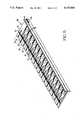
- FIG. 5is a perspective view of an array of radiators illustrated in FIG. 2;
- FIGS. 6A-6Dare plan views of various notch radiators employing impedance matching according to the present invention.
- a single radiating element in accordance with present inventionis illustrated in exploded prospective view. It should be understood, however, that a plurality of such elements 50 maybe provided in an array as hereinafter described.
- a dielectric substrate 52has a stripline 54 embedded therein.
- the impedance of the stripline 54is typically 50 ohm.
- the stripline 54has a terminal end 56 for coupling signals thereto and a feed end 58 which extends transversely of the stripline 54.
- the length of the feed end 58is one quarter wavelength ( ⁇ /4) of a selected frequency of interest.
- the dielectric 52is shaped as shown and as hereinafter described.
- a planar conductive housing 60 having a stepped recess 61receives the dielectric 52 in a lower portion 62 as illustrated.
- the shape of the dielectric 52conforms to the shape of the lower portion 62.
- the stepped recess 61has an upper portion 63 adjacent the lower portion 62 and a conductive cover 64 is adapted to be located in the upper portion 63 over the dielectric 52 and in electrical contact with the housing 60.
- the cover 64has a mating surface 66 which is designed to mate with the upper portion 63 and contact side walls 65 of the housing 60.
- the side walls 65isolate adjacent elements from spurious signals.
- the housing 60 and the cover 64have respective aligned elongated slots 70 and 72 as shown.
- the slots 70-72are aligned axially of the housing 60 and cover 64.
- the dielectric 52is located in the first recess portion 62 such that the feed end 58 of the stripline 54 lies transversely with respect to the slots 70-72.
- Respective terminal ends 74-76 of the slots 70-72lie one quarter wavelength from where the center of the feed end 58 crosses the slots 70-72 thereby forming quarter wavelength ( ⁇ /4) extensions 77-79. See for example the schematic illustration in FIGS. 3 and 4 showing the geometrical relationship between the feed end 58 of the stripline 54 and the slots 70-72.
- the slots 70 and 72are interconnected with a tapered aperture portion 78 formed in the housing 60 which extends from the slots 70-72 to a leading edge 80 of the element 50.
- FIG. 5illustrates a plurality of elements 50 in an elongated array 90.
- the dielectric 52(FIG. 2) is located in the first recess portion 62 and the cover 64 is located in the second recess portion 63.
- the array 90has a mounting flange 92 and slotted apertures 94 for receiving the terminal ends 95 of the dielectric 52 and the corresponding terminal end 56 of each of the striplines 54.
- the array 90may be employed as part of a phased array transmit/receive antenna.
- the output end 82 of each element 50tapers as shown.
- the purpose of this taperis to reduce structural cross polarization reflections at the aperture. It has been found, however, that performance is not adversely affected when the output end 82 of the elements is optimally untapered or square which allows for ease of manufacture.
- the first and second recess portions 62, 63, the cover 64 and the optional tapered output end 82are machined from aluminum stock. If desired one or more circulator chambers 99 may be provided as room permits.
- the slots 70-72 and tapered aperture portion 78may be machined using an electric discharge machining (EDM) technique.
- EDMelectric discharge machining
- FIG. 6Aillustrates a matched bilateral slot line antenna element 100 according to another embodiment of the invention.
- the stripline 102feeds the aperture 104 in a manner similar to the arrangements hereinbefore described.
- the aperture 104is formed of a conductor 106 having a narrow aperture launch portion or slot line transition 108 for launching the radiation, a relatively wide inductive notch or integrated matching discontinuity 110 and a step transition 112 therebetween.
- a floating septum 114 in the form of metallized filmmay be supported within the dielectric (not shown) in the same way as the stripline 102.
- the discontinuity 110has a width W which controls the impedance and a length L which controls the resonance of the device.
- the values of L and Wmay be iteratively determined for optimum results.
- the transition 112adds reactive impedance to the circuit for matching the slot line transition 108 with the discontinuity 110.
- the septum 114may be sized both in its length 1 and width w to fine tune the reactive impedance of the discontinuity 110 in order to obtain the desired response.
- the desired responseis a VSWR of 2:1 or lower over its bandwidth.
- the arrangement illustrated in FIG. 6Aprovides a somewhat narrow bandwidth of 8-12 GHz useful in some radar applications.
- FIG. 6Billustrates an impedance matching antenna element 120 which employs a tapered notch radiator 122 having a reactive iris 124 located at the aperture/free space discontinuity, that is, at the radiator output aperture 126.
- the stripline 128feeds the slot line transition 130 which tapers outwardly along boundary 132 to the aperture 126.
- the iris 124loads the antenna element 120 with an impedance which tunes the device.
- the width W of the aperture 126controls the impedance and the length L controls the reactance.
- the iris 124provides for a more symmetrical and centered output and reduces the VSWR over the bandwidth of the device.
- FIG. 6Cillustrates a resonant antenna element 140 having an integrated matching discontinuity 142, a step transition 144 and a slot line transition 146 for launching a signal from the stripline 148.
- the arrangementis similar to FIG. 6A.
- a resonant cavity 150is provided adjacent the discontinuity 142 for frequency control.
- the exact size and shape (i.e. square, rectangular or notched) of the resonant cavitymay be determined in accordance with desired frequency of operation and other relevant parameters.
- FIG. 6Dillustrates an impedance matched element 160 in which the quarter wavelength extension 162 is widened to provide an increased impedance at the interface of the stripline 164 and the slot line transition 166.
- the stripline 164is terminated with an open circuit stub 168.
- the arrangementbroadens the response of the coupler from 8-12 GHz to about 13-18 GHz.
- the mismatch provided by the open aperture 162 and the open circuit stub 168slightly raises the VSWR characteristic but not to an unacceptable level.
- FIGS. 6A--6Dmay be employed in the array illustrated in FIG. 2.
- the various aperturesmay be machined by various techniques including electrical discharge machining resulting in high precision apertures.
- the striplines in the various modified formsmay be printed and encapsulated within the dielectric.
Landscapes
- Waveguide Aerials (AREA)
Abstract
Description
Claims (20)
Priority Applications (1)
| Application Number | Priority Date | Filing Date | Title |
|---|---|---|---|
| US07/674,003US5175560A (en) | 1991-03-25 | 1991-03-25 | Notch radiator elements |
Applications Claiming Priority (1)
| Application Number | Priority Date | Filing Date | Title |
|---|---|---|---|
| US07/674,003US5175560A (en) | 1991-03-25 | 1991-03-25 | Notch radiator elements |
Publications (1)
| Publication Number | Publication Date |
|---|---|
| US5175560Atrue US5175560A (en) | 1992-12-29 |
Family
ID=24704945
Family Applications (1)
| Application Number | Title | Priority Date | Filing Date |
|---|---|---|---|
| US07/674,003Expired - LifetimeUS5175560A (en) | 1991-03-25 | 1991-03-25 | Notch radiator elements |
Country Status (1)
| Country | Link |
|---|---|
| US (1) | US5175560A (en) |
Cited By (140)
| Publication number | Priority date | Publication date | Assignee | Title |
|---|---|---|---|---|
| US5309165A (en)* | 1992-05-09 | 1994-05-03 | Westinghouse Electric Corp. | Positioner with corner contacts for cross notch array and improved radiator elements |
| US5532643A (en)* | 1995-06-23 | 1996-07-02 | Motorola, Inc. | Manufacturably improved asymmetric stripline enhanced aperture coupler |
| US5594456A (en)* | 1994-09-07 | 1997-01-14 | Patriot Scientific Corporation | Gas tube RF antenna |
| US6208308B1 (en)* | 1994-06-02 | 2001-03-27 | Raytheon Company | Polyrod antenna with flared notch feed |
| US6317094B1 (en)* | 1999-05-24 | 2001-11-13 | Litva Antenna Enterprises Inc. | Feed structures for tapered slot antennas |
| US6344830B1 (en) | 2000-08-14 | 2002-02-05 | Harris Corporation | Phased array antenna element having flared radiating leg elements |
| US6356240B1 (en)* | 2000-08-14 | 2002-03-12 | Harris Corporation | Phased array antenna element with straight v-configuration radiating leg elements |
| US6369763B1 (en) | 2000-04-05 | 2002-04-09 | Asi Technology Corporation | Reconfigurable plasma antenna |
| US6600453B1 (en)* | 2002-01-31 | 2003-07-29 | Raytheon Company | Surface/traveling wave suppressor for antenna arrays of notch radiators |
| US6624719B1 (en) | 2000-04-05 | 2003-09-23 | Asi Technology Corporation | Reconfigurable electromagnetic waveguide |
| US6700546B2 (en)* | 2000-01-05 | 2004-03-02 | Construction Diffusion Vente Internationale- Societe Anonyme | Elecronic key reader |
| US6710746B1 (en) | 2002-09-30 | 2004-03-23 | Markland Technologies, Inc. | Antenna having reconfigurable length |
| US20040130497A1 (en)* | 2002-07-17 | 2004-07-08 | Asi Technology Corporation | Reconfigurable antennas |
| US6812895B2 (en) | 2000-04-05 | 2004-11-02 | Markland Technologies, Inc. | Reconfigurable electromagnetic plasma waveguide used as a phase shifter and a horn antenna |
| US6850204B1 (en)* | 2002-11-07 | 2005-02-01 | Lockheed Martin Corporation | Clip for radar array, and array including the clip |
| US20090009390A1 (en)* | 2007-07-03 | 2009-01-08 | Northrop Grumman Systems Corporation | Dual band quadpack transmit/receive module |
| US20090322636A1 (en)* | 2007-05-30 | 2009-12-31 | Massachusetts Institute Of Technology | Notch antenna having a low profile stripline feed |
| US7884773B1 (en)* | 2006-04-27 | 2011-02-08 | Lockheed Martin Corporation | Horn antenna array |
| WO2011095969A1 (en)* | 2010-02-02 | 2011-08-11 | Technion Research & Development Foundation Ltd. | Compact tapered slot antenna |
| US20140218251A1 (en)* | 2013-02-04 | 2014-08-07 | Donald P. Waschenko | Notch-Antenna Array and Method for Making Same |
| US20140285388A1 (en)* | 2013-03-25 | 2014-09-25 | Farfield Co. | Broadband notch antennas |
| US20140354496A1 (en)* | 2013-05-30 | 2014-12-04 | Emw Co., Ltd. | Antenna |
| US20160134021A1 (en)* | 2014-11-06 | 2016-05-12 | Sony Corporation | Stripline coupled antenna with periodic slots for wireless electronic devices |
| US9674711B2 (en) | 2013-11-06 | 2017-06-06 | At&T Intellectual Property I, L.P. | Surface-wave communications and methods thereof |
| US9685992B2 (en) | 2014-10-03 | 2017-06-20 | At&T Intellectual Property I, L.P. | Circuit panel network and methods thereof |
| US9705561B2 (en) | 2015-04-24 | 2017-07-11 | At&T Intellectual Property I, L.P. | Directional coupling device and methods for use therewith |
| US9705610B2 (en) | 2014-10-21 | 2017-07-11 | At&T Intellectual Property I, L.P. | Transmission device with impairment compensation and methods for use therewith |
| US9729197B2 (en) | 2015-10-01 | 2017-08-08 | At&T Intellectual Property I, L.P. | Method and apparatus for communicating network management traffic over a network |
| US9735833B2 (en) | 2015-07-31 | 2017-08-15 | At&T Intellectual Property I, L.P. | Method and apparatus for communications management in a neighborhood network |
| US9742521B2 (en) | 2014-11-20 | 2017-08-22 | At&T Intellectual Property I, L.P. | Transmission device with mode division multiplexing and methods for use therewith |
| US9742462B2 (en) | 2014-12-04 | 2017-08-22 | At&T Intellectual Property I, L.P. | Transmission medium and communication interfaces and methods for use therewith |
| US9749053B2 (en) | 2015-07-23 | 2017-08-29 | At&T Intellectual Property I, L.P. | Node device, repeater and methods for use therewith |
| US9748626B2 (en) | 2015-05-14 | 2017-08-29 | At&T Intellectual Property I, L.P. | Plurality of cables having different cross-sectional shapes which are bundled together to form a transmission medium |
| US9749013B2 (en) | 2015-03-17 | 2017-08-29 | At&T Intellectual Property I, L.P. | Method and apparatus for reducing attenuation of electromagnetic waves guided by a transmission medium |
| US20170264006A1 (en)* | 2014-11-14 | 2017-09-14 | Mitsubishi Electric Corporation | Antenna device |
| US9769128B2 (en) | 2015-09-28 | 2017-09-19 | At&T Intellectual Property I, L.P. | Method and apparatus for encryption of communications over a network |
| US9769020B2 (en) | 2014-10-21 | 2017-09-19 | At&T Intellectual Property I, L.P. | Method and apparatus for responding to events affecting communications in a communication network |
| US9768833B2 (en) | 2014-09-15 | 2017-09-19 | At&T Intellectual Property I, L.P. | Method and apparatus for sensing a condition in a transmission medium of electromagnetic waves |
| US9780834B2 (en) | 2014-10-21 | 2017-10-03 | At&T Intellectual Property I, L.P. | Method and apparatus for transmitting electromagnetic waves |
| US9787412B2 (en) | 2015-06-25 | 2017-10-10 | At&T Intellectual Property I, L.P. | Methods and apparatus for inducing a fundamental wave mode on a transmission medium |
| US9793954B2 (en) | 2015-04-28 | 2017-10-17 | At&T Intellectual Property I, L.P. | Magnetic coupling device and methods for use therewith |
| US9793955B2 (en) | 2015-04-24 | 2017-10-17 | At&T Intellectual Property I, Lp | Passive electrical coupling device and methods for use therewith |
| US9800327B2 (en) | 2014-11-20 | 2017-10-24 | At&T Intellectual Property I, L.P. | Apparatus for controlling operations of a communication device and methods thereof |
| US9820146B2 (en) | 2015-06-12 | 2017-11-14 | At&T Intellectual Property I, L.P. | Method and apparatus for authentication and identity management of communicating devices |
| US9838896B1 (en) | 2016-12-09 | 2017-12-05 | At&T Intellectual Property I, L.P. | Method and apparatus for assessing network coverage |
| US9838078B2 (en) | 2015-07-31 | 2017-12-05 | At&T Intellectual Property I, L.P. | Method and apparatus for exchanging communication signals |
| US9847850B2 (en) | 2014-10-14 | 2017-12-19 | At&T Intellectual Property I, L.P. | Method and apparatus for adjusting a mode of communication in a communication network |
| US9847566B2 (en) | 2015-07-14 | 2017-12-19 | At&T Intellectual Property I, L.P. | Method and apparatus for adjusting a field of a signal to mitigate interference |
| US9853342B2 (en) | 2015-07-14 | 2017-12-26 | At&T Intellectual Property I, L.P. | Dielectric transmission medium connector and methods for use therewith |
| US9860075B1 (en) | 2016-08-26 | 2018-01-02 | At&T Intellectual Property I, L.P. | Method and communication node for broadband distribution |
| US9866309B2 (en) | 2015-06-03 | 2018-01-09 | At&T Intellectual Property I, Lp | Host node device and methods for use therewith |
| US9865911B2 (en) | 2015-06-25 | 2018-01-09 | At&T Intellectual Property I, L.P. | Waveguide system for slot radiating first electromagnetic waves that are combined into a non-fundamental wave mode second electromagnetic wave on a transmission medium |
| US9866276B2 (en) | 2014-10-10 | 2018-01-09 | At&T Intellectual Property I, L.P. | Method and apparatus for arranging communication sessions in a communication system |
| US9871283B2 (en) | 2015-07-23 | 2018-01-16 | At&T Intellectual Property I, Lp | Transmission medium having a dielectric core comprised of plural members connected by a ball and socket configuration |
| US9871558B2 (en) | 2014-10-21 | 2018-01-16 | At&T Intellectual Property I, L.P. | Guided-wave transmission device and methods for use therewith |
| US9871282B2 (en) | 2015-05-14 | 2018-01-16 | At&T Intellectual Property I, L.P. | At least one transmission medium having a dielectric surface that is covered at least in part by a second dielectric |
| US9876571B2 (en) | 2015-02-20 | 2018-01-23 | At&T Intellectual Property I, Lp | Guided-wave transmission device with non-fundamental mode propagation and methods for use therewith |
| US9876264B2 (en) | 2015-10-02 | 2018-01-23 | At&T Intellectual Property I, Lp | Communication system, guided wave switch and methods for use therewith |
| US9882257B2 (en) | 2015-07-14 | 2018-01-30 | At&T Intellectual Property I, L.P. | Method and apparatus for launching a wave mode that mitigates interference |
| US9887447B2 (en) | 2015-05-14 | 2018-02-06 | At&T Intellectual Property I, L.P. | Transmission medium having multiple cores and methods for use therewith |
| US9893795B1 (en) | 2016-12-07 | 2018-02-13 | At&T Intellectual Property I, Lp | Method and repeater for broadband distribution |
| US9906269B2 (en) | 2014-09-17 | 2018-02-27 | At&T Intellectual Property I, L.P. | Monitoring and mitigating conditions in a communication network |
| US9904535B2 (en) | 2015-09-14 | 2018-02-27 | At&T Intellectual Property I, L.P. | Method and apparatus for distributing software |
| US9912381B2 (en) | 2015-06-03 | 2018-03-06 | At&T Intellectual Property I, Lp | Network termination and methods for use therewith |
| US9912027B2 (en) | 2015-07-23 | 2018-03-06 | At&T Intellectual Property I, L.P. | Method and apparatus for exchanging communication signals |
| US9912033B2 (en) | 2014-10-21 | 2018-03-06 | At&T Intellectual Property I, Lp | Guided wave coupler, coupling module and methods for use therewith |
| US9913139B2 (en) | 2015-06-09 | 2018-03-06 | At&T Intellectual Property I, L.P. | Signal fingerprinting for authentication of communicating devices |
| US9911020B1 (en) | 2016-12-08 | 2018-03-06 | At&T Intellectual Property I, L.P. | Method and apparatus for tracking via a radio frequency identification device |
| US9917341B2 (en) | 2015-05-27 | 2018-03-13 | At&T Intellectual Property I, L.P. | Apparatus and method for launching electromagnetic waves and for modifying radial dimensions of the propagating electromagnetic waves |
| US9927517B1 (en) | 2016-12-06 | 2018-03-27 | At&T Intellectual Property I, L.P. | Apparatus and methods for sensing rainfall |
| US9929755B2 (en) | 2015-07-14 | 2018-03-27 | At&T Intellectual Property I, L.P. | Method and apparatus for coupling an antenna to a device |
| US9948333B2 (en) | 2015-07-23 | 2018-04-17 | At&T Intellectual Property I, L.P. | Method and apparatus for wireless communications to mitigate interference |
| US9954286B2 (en) | 2014-10-21 | 2018-04-24 | At&T Intellectual Property I, L.P. | Guided-wave transmission device with non-fundamental mode propagation and methods for use therewith |
| US9954287B2 (en) | 2014-11-20 | 2018-04-24 | At&T Intellectual Property I, L.P. | Apparatus for converting wireless signals and electromagnetic waves and methods thereof |
| US9967173B2 (en) | 2015-07-31 | 2018-05-08 | At&T Intellectual Property I, L.P. | Method and apparatus for authentication and identity management of communicating devices |
| US9973940B1 (en) | 2017-02-27 | 2018-05-15 | At&T Intellectual Property I, L.P. | Apparatus and methods for dynamic impedance matching of a guided wave launcher |
| US9973416B2 (en) | 2014-10-02 | 2018-05-15 | At&T Intellectual Property I, L.P. | Method and apparatus that provides fault tolerance in a communication network |
| US9998870B1 (en) | 2016-12-08 | 2018-06-12 | At&T Intellectual Property I, L.P. | Method and apparatus for proximity sensing |
| US9997819B2 (en) | 2015-06-09 | 2018-06-12 | At&T Intellectual Property I, L.P. | Transmission medium and method for facilitating propagation of electromagnetic waves via a core |
| US9999038B2 (en) | 2013-05-31 | 2018-06-12 | At&T Intellectual Property I, L.P. | Remote distributed antenna system |
| US10009067B2 (en) | 2014-12-04 | 2018-06-26 | At&T Intellectual Property I, L.P. | Method and apparatus for configuring a communication interface |
| US10020844B2 (en) | 2016-12-06 | 2018-07-10 | T&T Intellectual Property I, L.P. | Method and apparatus for broadcast communication via guided waves |
| US10027397B2 (en) | 2016-12-07 | 2018-07-17 | At&T Intellectual Property I, L.P. | Distributed antenna system and methods for use therewith |
| US10044409B2 (en) | 2015-07-14 | 2018-08-07 | At&T Intellectual Property I, L.P. | Transmission medium and methods for use therewith |
| US10051630B2 (en) | 2013-05-31 | 2018-08-14 | At&T Intellectual Property I, L.P. | Remote distributed antenna system |
| US10069185B2 (en) | 2015-06-25 | 2018-09-04 | At&T Intellectual Property I, L.P. | Methods and apparatus for inducing a non-fundamental wave mode on a transmission medium |
| US10069535B2 (en) | 2016-12-08 | 2018-09-04 | At&T Intellectual Property I, L.P. | Apparatus and methods for launching electromagnetic waves having a certain electric field structure |
| US10090606B2 (en) | 2015-07-15 | 2018-10-02 | At&T Intellectual Property I, L.P. | Antenna system with dielectric array and methods for use therewith |
| US10090594B2 (en) | 2016-11-23 | 2018-10-02 | At&T Intellectual Property I, L.P. | Antenna system having structural configurations for assembly |
| US10103422B2 (en) | 2016-12-08 | 2018-10-16 | At&T Intellectual Property I, L.P. | Method and apparatus for mounting network devices |
| EP3266066A4 (en)* | 2015-03-03 | 2018-10-31 | The Government of the United States of America as represented by the Secretary of the Navy | Low cross-polarization decade-bandwidth ultra-wideband antenna element and array |
| US10135145B2 (en) | 2016-12-06 | 2018-11-20 | At&T Intellectual Property I, L.P. | Apparatus and methods for generating an electromagnetic wave along a transmission medium |
| US10139820B2 (en) | 2016-12-07 | 2018-11-27 | At&T Intellectual Property I, L.P. | Method and apparatus for deploying equipment of a communication system |
| US10148016B2 (en) | 2015-07-14 | 2018-12-04 | At&T Intellectual Property I, L.P. | Apparatus and methods for communicating utilizing an antenna array |
| US10168695B2 (en) | 2016-12-07 | 2019-01-01 | At&T Intellectual Property I, L.P. | Method and apparatus for controlling an unmanned aircraft |
| US10178445B2 (en) | 2016-11-23 | 2019-01-08 | At&T Intellectual Property I, L.P. | Methods, devices, and systems for load balancing between a plurality of waveguides |
| US10205655B2 (en) | 2015-07-14 | 2019-02-12 | At&T Intellectual Property I, L.P. | Apparatus and methods for communicating utilizing an antenna array and multiple communication paths |
| US10225025B2 (en) | 2016-11-03 | 2019-03-05 | At&T Intellectual Property I, L.P. | Method and apparatus for detecting a fault in a communication system |
| US10224634B2 (en) | 2016-11-03 | 2019-03-05 | At&T Intellectual Property I, L.P. | Methods and apparatus for adjusting an operational characteristic of an antenna |
| US10243270B2 (en) | 2016-12-07 | 2019-03-26 | At&T Intellectual Property I, L.P. | Beam adaptive multi-feed dielectric antenna system and methods for use therewith |
| US10243784B2 (en) | 2014-11-20 | 2019-03-26 | At&T Intellectual Property I, L.P. | System for generating topology information and methods thereof |
| US10264586B2 (en) | 2016-12-09 | 2019-04-16 | At&T Mobility Ii Llc | Cloud-based packet controller and methods for use therewith |
| US10291334B2 (en) | 2016-11-03 | 2019-05-14 | At&T Intellectual Property I, L.P. | System for detecting a fault in a communication system |
| US10298293B2 (en) | 2017-03-13 | 2019-05-21 | At&T Intellectual Property I, L.P. | Apparatus of communication utilizing wireless network devices |
| US10305190B2 (en) | 2016-12-01 | 2019-05-28 | At&T Intellectual Property I, L.P. | Reflecting dielectric antenna system and methods for use therewith |
| US10312567B2 (en) | 2016-10-26 | 2019-06-04 | At&T Intellectual Property I, L.P. | Launcher with planar strip antenna and methods for use therewith |
| US10326689B2 (en) | 2016-12-08 | 2019-06-18 | At&T Intellectual Property I, L.P. | Method and system for providing alternative communication paths |
| US10326494B2 (en) | 2016-12-06 | 2019-06-18 | At&T Intellectual Property I, L.P. | Apparatus for measurement de-embedding and methods for use therewith |
| US10340603B2 (en) | 2016-11-23 | 2019-07-02 | At&T Intellectual Property I, L.P. | Antenna system having shielded structural configurations for assembly |
| US10340573B2 (en) | 2016-10-26 | 2019-07-02 | At&T Intellectual Property I, L.P. | Launcher with cylindrical coupling device and methods for use therewith |
| US10340601B2 (en) | 2016-11-23 | 2019-07-02 | At&T Intellectual Property I, L.P. | Multi-antenna system and methods for use therewith |
| US10340983B2 (en) | 2016-12-09 | 2019-07-02 | At&T Intellectual Property I, L.P. | Method and apparatus for surveying remote sites via guided wave communications |
| US10355367B2 (en) | 2015-10-16 | 2019-07-16 | At&T Intellectual Property I, L.P. | Antenna structure for exchanging wireless signals |
| US10361489B2 (en) | 2016-12-01 | 2019-07-23 | At&T Intellectual Property I, L.P. | Dielectric dish antenna system and methods for use therewith |
| US10359749B2 (en) | 2016-12-07 | 2019-07-23 | At&T Intellectual Property I, L.P. | Method and apparatus for utilities management via guided wave communication |
| US10374316B2 (en) | 2016-10-21 | 2019-08-06 | At&T Intellectual Property I, L.P. | System and dielectric antenna with non-uniform dielectric |
| US10382976B2 (en) | 2016-12-06 | 2019-08-13 | At&T Intellectual Property I, L.P. | Method and apparatus for managing wireless communications based on communication paths and network device positions |
| US10389029B2 (en) | 2016-12-07 | 2019-08-20 | At&T Intellectual Property I, L.P. | Multi-feed dielectric antenna system with core selection and methods for use therewith |
| US10389037B2 (en) | 2016-12-08 | 2019-08-20 | At&T Intellectual Property I, L.P. | Apparatus and methods for selecting sections of an antenna array and use therewith |
| US10411356B2 (en) | 2016-12-08 | 2019-09-10 | At&T Intellectual Property I, L.P. | Apparatus and methods for selectively targeting communication devices with an antenna array |
| US10439675B2 (en) | 2016-12-06 | 2019-10-08 | At&T Intellectual Property I, L.P. | Method and apparatus for repeating guided wave communication signals |
| US10446936B2 (en) | 2016-12-07 | 2019-10-15 | At&T Intellectual Property I, L.P. | Multi-feed dielectric antenna system and methods for use therewith |
| US10498044B2 (en) | 2016-11-03 | 2019-12-03 | At&T Intellectual Property I, L.P. | Apparatus for configuring a surface of an antenna |
| US10530505B2 (en) | 2016-12-08 | 2020-01-07 | At&T Intellectual Property I, L.P. | Apparatus and methods for launching electromagnetic waves along a transmission medium |
| US10535928B2 (en) | 2016-11-23 | 2020-01-14 | At&T Intellectual Property I, L.P. | Antenna system and methods for use therewith |
| US10547348B2 (en) | 2016-12-07 | 2020-01-28 | At&T Intellectual Property I, L.P. | Method and apparatus for switching transmission mediums in a communication system |
| US10547105B2 (en) | 2017-03-02 | 2020-01-28 | The Government Of The United States Of America, As Represented By The Secretary Of The Navy | Superstrate polarization and impedance rectifying elements |
| US10601494B2 (en) | 2016-12-08 | 2020-03-24 | At&T Intellectual Property I, L.P. | Dual-band communication device and method for use therewith |
| US10637149B2 (en) | 2016-12-06 | 2020-04-28 | At&T Intellectual Property I, L.P. | Injection molded dielectric antenna and methods for use therewith |
| US10650940B2 (en) | 2015-05-15 | 2020-05-12 | At&T Intellectual Property I, L.P. | Transmission medium having a conductive material and methods for use therewith |
| US10694379B2 (en) | 2016-12-06 | 2020-06-23 | At&T Intellectual Property I, L.P. | Waveguide system with device-based authentication and methods for use therewith |
| US10727599B2 (en) | 2016-12-06 | 2020-07-28 | At&T Intellectual Property I, L.P. | Launcher with slot antenna and methods for use therewith |
| US10755542B2 (en) | 2016-12-06 | 2020-08-25 | At&T Intellectual Property I, L.P. | Method and apparatus for surveillance via guided wave communication |
| US10777873B2 (en) | 2016-12-08 | 2020-09-15 | At&T Intellectual Property I, L.P. | Method and apparatus for mounting network devices |
| US10797781B2 (en) | 2015-06-03 | 2020-10-06 | At&T Intellectual Property I, L.P. | Client node device and methods for use therewith |
| US10811767B2 (en) | 2016-10-21 | 2020-10-20 | At&T Intellectual Property I, L.P. | System and dielectric antenna with convex dielectric radome |
| US10819035B2 (en) | 2016-12-06 | 2020-10-27 | At&T Intellectual Property I, L.P. | Launcher with helical antenna and methods for use therewith |
| US10916969B2 (en) | 2016-12-08 | 2021-02-09 | At&T Intellectual Property I, L.P. | Method and apparatus for providing power using an inductive coupling |
| US10938108B2 (en) | 2016-12-08 | 2021-03-02 | At&T Intellectual Property I, L.P. | Frequency selective multi-feed dielectric antenna system and methods for use therewith |
| US20220217656A1 (en)* | 2019-09-23 | 2022-07-07 | Qualcomm Incorporated | Antenna module placement and housing for reduced power density exposure |
Citations (5)
| Publication number | Priority date | Publication date | Assignee | Title |
|---|---|---|---|---|
| US4001834A (en)* | 1975-04-08 | 1977-01-04 | Aeronutronic Ford Corporation | Printed wiring antenna and arrays fabricated thereof |
| US4353072A (en)* | 1980-11-24 | 1982-10-05 | Raytheon Company | Circularly polarized radio frequency antenna |
| US4573056A (en)* | 1981-12-18 | 1986-02-25 | Thomson Csf | Dipole radiator excited by a shielded slot line |
| US4672384A (en)* | 1984-12-31 | 1987-06-09 | Raytheon Company | Circularly polarized radio frequency antenna |
| US5023623A (en)* | 1989-12-21 | 1991-06-11 | Hughes Aircraft Company | Dual mode antenna apparatus having slotted waveguide and broadband arrays |
- 1991
- 1991-03-25USUS07/674,003patent/US5175560A/ennot_activeExpired - Lifetime
Patent Citations (5)
| Publication number | Priority date | Publication date | Assignee | Title |
|---|---|---|---|---|
| US4001834A (en)* | 1975-04-08 | 1977-01-04 | Aeronutronic Ford Corporation | Printed wiring antenna and arrays fabricated thereof |
| US4353072A (en)* | 1980-11-24 | 1982-10-05 | Raytheon Company | Circularly polarized radio frequency antenna |
| US4573056A (en)* | 1981-12-18 | 1986-02-25 | Thomson Csf | Dipole radiator excited by a shielded slot line |
| US4672384A (en)* | 1984-12-31 | 1987-06-09 | Raytheon Company | Circularly polarized radio frequency antenna |
| US5023623A (en)* | 1989-12-21 | 1991-06-11 | Hughes Aircraft Company | Dual mode antenna apparatus having slotted waveguide and broadband arrays |
Cited By (171)
| Publication number | Priority date | Publication date | Assignee | Title |
|---|---|---|---|---|
| US5309165A (en)* | 1992-05-09 | 1994-05-03 | Westinghouse Electric Corp. | Positioner with corner contacts for cross notch array and improved radiator elements |
| US6208308B1 (en)* | 1994-06-02 | 2001-03-27 | Raytheon Company | Polyrod antenna with flared notch feed |
| US5594456A (en)* | 1994-09-07 | 1997-01-14 | Patriot Scientific Corporation | Gas tube RF antenna |
| WO1998008269A1 (en)* | 1994-09-07 | 1998-02-26 | Patriot Scientific Corporation | Gas tube rf antenna |
| US5532643A (en)* | 1995-06-23 | 1996-07-02 | Motorola, Inc. | Manufacturably improved asymmetric stripline enhanced aperture coupler |
| US6317094B1 (en)* | 1999-05-24 | 2001-11-13 | Litva Antenna Enterprises Inc. | Feed structures for tapered slot antennas |
| US6700546B2 (en)* | 2000-01-05 | 2004-03-02 | Construction Diffusion Vente Internationale- Societe Anonyme | Elecronic key reader |
| US6812895B2 (en) | 2000-04-05 | 2004-11-02 | Markland Technologies, Inc. | Reconfigurable electromagnetic plasma waveguide used as a phase shifter and a horn antenna |
| US6369763B1 (en) | 2000-04-05 | 2002-04-09 | Asi Technology Corporation | Reconfigurable plasma antenna |
| US6624719B1 (en) | 2000-04-05 | 2003-09-23 | Asi Technology Corporation | Reconfigurable electromagnetic waveguide |
| US6356240B1 (en)* | 2000-08-14 | 2002-03-12 | Harris Corporation | Phased array antenna element with straight v-configuration radiating leg elements |
| US6344830B1 (en) | 2000-08-14 | 2002-02-05 | Harris Corporation | Phased array antenna element having flared radiating leg elements |
| US6600453B1 (en)* | 2002-01-31 | 2003-07-29 | Raytheon Company | Surface/traveling wave suppressor for antenna arrays of notch radiators |
| US20030142026A1 (en)* | 2002-01-31 | 2003-07-31 | Hadden John M. | Surface/traveling wave suppressor for antenna arrays of notch radiators |
| US20040130497A1 (en)* | 2002-07-17 | 2004-07-08 | Asi Technology Corporation | Reconfigurable antennas |
| US6876330B2 (en) | 2002-07-17 | 2005-04-05 | Markland Technologies, Inc. | Reconfigurable antennas |
| US6710746B1 (en) | 2002-09-30 | 2004-03-23 | Markland Technologies, Inc. | Antenna having reconfigurable length |
| US6850204B1 (en)* | 2002-11-07 | 2005-02-01 | Lockheed Martin Corporation | Clip for radar array, and array including the clip |
| US7884773B1 (en)* | 2006-04-27 | 2011-02-08 | Lockheed Martin Corporation | Horn antenna array |
| US20090322636A1 (en)* | 2007-05-30 | 2009-12-31 | Massachusetts Institute Of Technology | Notch antenna having a low profile stripline feed |
| US8350767B2 (en) | 2007-05-30 | 2013-01-08 | Massachusetts Institute Of Technology | Notch antenna having a low profile stripline feed |
| US7728771B2 (en) | 2007-07-03 | 2010-06-01 | Northrop Grumman Systems Corporation | Dual band quadpack transmit/receive module |
| US20090009390A1 (en)* | 2007-07-03 | 2009-01-08 | Northrop Grumman Systems Corporation | Dual band quadpack transmit/receive module |
| WO2011095969A1 (en)* | 2010-02-02 | 2011-08-11 | Technion Research & Development Foundation Ltd. | Compact tapered slot antenna |
| US9142889B2 (en) | 2010-02-02 | 2015-09-22 | Technion Research & Development Foundation Ltd. | Compact tapered slot antenna |
| US20140218251A1 (en)* | 2013-02-04 | 2014-08-07 | Donald P. Waschenko | Notch-Antenna Array and Method for Making Same |
| WO2014121212A1 (en)* | 2013-02-04 | 2014-08-07 | Sensor And Antenna Systems, Lansdale, Inc. | Notch-antenna array and method of making same |
| US9270027B2 (en)* | 2013-02-04 | 2016-02-23 | Sensor And Antenna Systems, Lansdale, Inc. | Notch-antenna array and method for making same |
| US9601833B2 (en)* | 2013-03-25 | 2017-03-21 | Wavcatcher | Broadband notch antennas |
| US20140285388A1 (en)* | 2013-03-25 | 2014-09-25 | Farfield Co. | Broadband notch antennas |
| US20140354496A1 (en)* | 2013-05-30 | 2014-12-04 | Emw Co., Ltd. | Antenna |
| US9391372B2 (en)* | 2013-05-30 | 2016-07-12 | Emw Co., Ltd. | Antenna |
| US10051630B2 (en) | 2013-05-31 | 2018-08-14 | At&T Intellectual Property I, L.P. | Remote distributed antenna system |
| US9999038B2 (en) | 2013-05-31 | 2018-06-12 | At&T Intellectual Property I, L.P. | Remote distributed antenna system |
| US9674711B2 (en) | 2013-11-06 | 2017-06-06 | At&T Intellectual Property I, L.P. | Surface-wave communications and methods thereof |
| US9768833B2 (en) | 2014-09-15 | 2017-09-19 | At&T Intellectual Property I, L.P. | Method and apparatus for sensing a condition in a transmission medium of electromagnetic waves |
| US9906269B2 (en) | 2014-09-17 | 2018-02-27 | At&T Intellectual Property I, L.P. | Monitoring and mitigating conditions in a communication network |
| US10063280B2 (en) | 2014-09-17 | 2018-08-28 | At&T Intellectual Property I, L.P. | Monitoring and mitigating conditions in a communication network |
| US9973416B2 (en) | 2014-10-02 | 2018-05-15 | At&T Intellectual Property I, L.P. | Method and apparatus that provides fault tolerance in a communication network |
| US9685992B2 (en) | 2014-10-03 | 2017-06-20 | At&T Intellectual Property I, L.P. | Circuit panel network and methods thereof |
| US9866276B2 (en) | 2014-10-10 | 2018-01-09 | At&T Intellectual Property I, L.P. | Method and apparatus for arranging communication sessions in a communication system |
| US9847850B2 (en) | 2014-10-14 | 2017-12-19 | At&T Intellectual Property I, L.P. | Method and apparatus for adjusting a mode of communication in a communication network |
| US9705610B2 (en) | 2014-10-21 | 2017-07-11 | At&T Intellectual Property I, L.P. | Transmission device with impairment compensation and methods for use therewith |
| US9769020B2 (en) | 2014-10-21 | 2017-09-19 | At&T Intellectual Property I, L.P. | Method and apparatus for responding to events affecting communications in a communication network |
| US9871558B2 (en) | 2014-10-21 | 2018-01-16 | At&T Intellectual Property I, L.P. | Guided-wave transmission device and methods for use therewith |
| US9876587B2 (en) | 2014-10-21 | 2018-01-23 | At&T Intellectual Property I, L.P. | Transmission device with impairment compensation and methods for use therewith |
| US9954286B2 (en) | 2014-10-21 | 2018-04-24 | At&T Intellectual Property I, L.P. | Guided-wave transmission device with non-fundamental mode propagation and methods for use therewith |
| US9780834B2 (en) | 2014-10-21 | 2017-10-03 | At&T Intellectual Property I, L.P. | Method and apparatus for transmitting electromagnetic waves |
| US9960808B2 (en) | 2014-10-21 | 2018-05-01 | At&T Intellectual Property I, L.P. | Guided-wave transmission device and methods for use therewith |
| US9912033B2 (en) | 2014-10-21 | 2018-03-06 | At&T Intellectual Property I, Lp | Guided wave coupler, coupling module and methods for use therewith |
| CN107078380B (en)* | 2014-11-06 | 2020-01-03 | 索尼公司 | Wireless electronic device |
| CN107078380A (en)* | 2014-11-06 | 2017-08-18 | 索尼公司 | The strip line coupling antenna with periodicity groove for wireless electron device |
| US10103440B2 (en)* | 2014-11-06 | 2018-10-16 | Sony Mobile Communications Inc. | Stripline coupled antenna with periodic slots for wireless electronic devices |
| US20160134021A1 (en)* | 2014-11-06 | 2016-05-12 | Sony Corporation | Stripline coupled antenna with periodic slots for wireless electronic devices |
| KR20170067887A (en)* | 2014-11-06 | 2017-06-16 | 소니 주식회사 | Stripline coupled antenna with periodic slots for wireless electronic devices |
| JP2017533675A (en)* | 2014-11-06 | 2017-11-09 | ソニー株式会社 | Stripline coupled antenna with periodic slots for wireless electronic devices |
| US20170264006A1 (en)* | 2014-11-14 | 2017-09-14 | Mitsubishi Electric Corporation | Antenna device |
| US10181639B2 (en)* | 2014-11-14 | 2019-01-15 | Mitsubishi Electric Corporation | Antenna device |
| US9800327B2 (en) | 2014-11-20 | 2017-10-24 | At&T Intellectual Property I, L.P. | Apparatus for controlling operations of a communication device and methods thereof |
| US10243784B2 (en) | 2014-11-20 | 2019-03-26 | At&T Intellectual Property I, L.P. | System for generating topology information and methods thereof |
| US9742521B2 (en) | 2014-11-20 | 2017-08-22 | At&T Intellectual Property I, L.P. | Transmission device with mode division multiplexing and methods for use therewith |
| US9749083B2 (en) | 2014-11-20 | 2017-08-29 | At&T Intellectual Property I, L.P. | Transmission device with mode division multiplexing and methods for use therewith |
| US9954287B2 (en) | 2014-11-20 | 2018-04-24 | At&T Intellectual Property I, L.P. | Apparatus for converting wireless signals and electromagnetic waves and methods thereof |
| US9742462B2 (en) | 2014-12-04 | 2017-08-22 | At&T Intellectual Property I, L.P. | Transmission medium and communication interfaces and methods for use therewith |
| US10009067B2 (en) | 2014-12-04 | 2018-06-26 | At&T Intellectual Property I, L.P. | Method and apparatus for configuring a communication interface |
| US9876571B2 (en) | 2015-02-20 | 2018-01-23 | At&T Intellectual Property I, Lp | Guided-wave transmission device with non-fundamental mode propagation and methods for use therewith |
| US9876570B2 (en) | 2015-02-20 | 2018-01-23 | At&T Intellectual Property I, Lp | Guided-wave transmission device with non-fundamental mode propagation and methods for use therewith |
| EP3266066A4 (en)* | 2015-03-03 | 2018-10-31 | The Government of the United States of America as represented by the Secretary of the Navy | Low cross-polarization decade-bandwidth ultra-wideband antenna element and array |
| US10483655B2 (en) | 2015-03-03 | 2019-11-19 | University Of Massachusetts | Low cross-polarization decade-bandwidth ultra-wideband antenna element and array |
| US9749013B2 (en) | 2015-03-17 | 2017-08-29 | At&T Intellectual Property I, L.P. | Method and apparatus for reducing attenuation of electromagnetic waves guided by a transmission medium |
| US9831912B2 (en) | 2015-04-24 | 2017-11-28 | At&T Intellectual Property I, Lp | Directional coupling device and methods for use therewith |
| US9705561B2 (en) | 2015-04-24 | 2017-07-11 | At&T Intellectual Property I, L.P. | Directional coupling device and methods for use therewith |
| US10224981B2 (en) | 2015-04-24 | 2019-03-05 | At&T Intellectual Property I, Lp | Passive electrical coupling device and methods for use therewith |
| US9793955B2 (en) | 2015-04-24 | 2017-10-17 | At&T Intellectual Property I, Lp | Passive electrical coupling device and methods for use therewith |
| US9793954B2 (en) | 2015-04-28 | 2017-10-17 | At&T Intellectual Property I, L.P. | Magnetic coupling device and methods for use therewith |
| US9748626B2 (en) | 2015-05-14 | 2017-08-29 | At&T Intellectual Property I, L.P. | Plurality of cables having different cross-sectional shapes which are bundled together to form a transmission medium |
| US9871282B2 (en) | 2015-05-14 | 2018-01-16 | At&T Intellectual Property I, L.P. | At least one transmission medium having a dielectric surface that is covered at least in part by a second dielectric |
| US9887447B2 (en) | 2015-05-14 | 2018-02-06 | At&T Intellectual Property I, L.P. | Transmission medium having multiple cores and methods for use therewith |
| US10650940B2 (en) | 2015-05-15 | 2020-05-12 | At&T Intellectual Property I, L.P. | Transmission medium having a conductive material and methods for use therewith |
| US9917341B2 (en) | 2015-05-27 | 2018-03-13 | At&T Intellectual Property I, L.P. | Apparatus and method for launching electromagnetic waves and for modifying radial dimensions of the propagating electromagnetic waves |
| US9967002B2 (en) | 2015-06-03 | 2018-05-08 | At&T Intellectual I, Lp | Network termination and methods for use therewith |
| US9866309B2 (en) | 2015-06-03 | 2018-01-09 | At&T Intellectual Property I, Lp | Host node device and methods for use therewith |
| US10050697B2 (en) | 2015-06-03 | 2018-08-14 | At&T Intellectual Property I, L.P. | Host node device and methods for use therewith |
| US9912381B2 (en) | 2015-06-03 | 2018-03-06 | At&T Intellectual Property I, Lp | Network termination and methods for use therewith |
| US9912382B2 (en) | 2015-06-03 | 2018-03-06 | At&T Intellectual Property I, Lp | Network termination and methods for use therewith |
| US9935703B2 (en) | 2015-06-03 | 2018-04-03 | At&T Intellectual Property I, L.P. | Host node device and methods for use therewith |
| US10797781B2 (en) | 2015-06-03 | 2020-10-06 | At&T Intellectual Property I, L.P. | Client node device and methods for use therewith |
| US10812174B2 (en) | 2015-06-03 | 2020-10-20 | At&T Intellectual Property I, L.P. | Client node device and methods for use therewith |
| US9913139B2 (en) | 2015-06-09 | 2018-03-06 | At&T Intellectual Property I, L.P. | Signal fingerprinting for authentication of communicating devices |
| US9997819B2 (en) | 2015-06-09 | 2018-06-12 | At&T Intellectual Property I, L.P. | Transmission medium and method for facilitating propagation of electromagnetic waves via a core |
| US9820146B2 (en) | 2015-06-12 | 2017-11-14 | At&T Intellectual Property I, L.P. | Method and apparatus for authentication and identity management of communicating devices |
| US9787412B2 (en) | 2015-06-25 | 2017-10-10 | At&T Intellectual Property I, L.P. | Methods and apparatus for inducing a fundamental wave mode on a transmission medium |
| US9865911B2 (en) | 2015-06-25 | 2018-01-09 | At&T Intellectual Property I, L.P. | Waveguide system for slot radiating first electromagnetic waves that are combined into a non-fundamental wave mode second electromagnetic wave on a transmission medium |
| US10069185B2 (en) | 2015-06-25 | 2018-09-04 | At&T Intellectual Property I, L.P. | Methods and apparatus for inducing a non-fundamental wave mode on a transmission medium |
| US9847566B2 (en) | 2015-07-14 | 2017-12-19 | At&T Intellectual Property I, L.P. | Method and apparatus for adjusting a field of a signal to mitigate interference |
| US9929755B2 (en) | 2015-07-14 | 2018-03-27 | At&T Intellectual Property I, L.P. | Method and apparatus for coupling an antenna to a device |
| US10205655B2 (en) | 2015-07-14 | 2019-02-12 | At&T Intellectual Property I, L.P. | Apparatus and methods for communicating utilizing an antenna array and multiple communication paths |
| US10044409B2 (en) | 2015-07-14 | 2018-08-07 | At&T Intellectual Property I, L.P. | Transmission medium and methods for use therewith |
| US9882257B2 (en) | 2015-07-14 | 2018-01-30 | At&T Intellectual Property I, L.P. | Method and apparatus for launching a wave mode that mitigates interference |
| US9853342B2 (en) | 2015-07-14 | 2017-12-26 | At&T Intellectual Property I, L.P. | Dielectric transmission medium connector and methods for use therewith |
| US10148016B2 (en) | 2015-07-14 | 2018-12-04 | At&T Intellectual Property I, L.P. | Apparatus and methods for communicating utilizing an antenna array |
| US10090606B2 (en) | 2015-07-15 | 2018-10-02 | At&T Intellectual Property I, L.P. | Antenna system with dielectric array and methods for use therewith |
| US9912027B2 (en) | 2015-07-23 | 2018-03-06 | At&T Intellectual Property I, L.P. | Method and apparatus for exchanging communication signals |
| US9871283B2 (en) | 2015-07-23 | 2018-01-16 | At&T Intellectual Property I, Lp | Transmission medium having a dielectric core comprised of plural members connected by a ball and socket configuration |
| US9749053B2 (en) | 2015-07-23 | 2017-08-29 | At&T Intellectual Property I, L.P. | Node device, repeater and methods for use therewith |
| US9806818B2 (en) | 2015-07-23 | 2017-10-31 | At&T Intellectual Property I, Lp | Node device, repeater and methods for use therewith |
| US9948333B2 (en) | 2015-07-23 | 2018-04-17 | At&T Intellectual Property I, L.P. | Method and apparatus for wireless communications to mitigate interference |
| US9735833B2 (en) | 2015-07-31 | 2017-08-15 | At&T Intellectual Property I, L.P. | Method and apparatus for communications management in a neighborhood network |
| US9967173B2 (en) | 2015-07-31 | 2018-05-08 | At&T Intellectual Property I, L.P. | Method and apparatus for authentication and identity management of communicating devices |
| US9838078B2 (en) | 2015-07-31 | 2017-12-05 | At&T Intellectual Property I, L.P. | Method and apparatus for exchanging communication signals |
| US9904535B2 (en) | 2015-09-14 | 2018-02-27 | At&T Intellectual Property I, L.P. | Method and apparatus for distributing software |
| US9769128B2 (en) | 2015-09-28 | 2017-09-19 | At&T Intellectual Property I, L.P. | Method and apparatus for encryption of communications over a network |
| US9729197B2 (en) | 2015-10-01 | 2017-08-08 | At&T Intellectual Property I, L.P. | Method and apparatus for communicating network management traffic over a network |
| US9876264B2 (en) | 2015-10-02 | 2018-01-23 | At&T Intellectual Property I, Lp | Communication system, guided wave switch and methods for use therewith |
| US10355367B2 (en) | 2015-10-16 | 2019-07-16 | At&T Intellectual Property I, L.P. | Antenna structure for exchanging wireless signals |
| US9860075B1 (en) | 2016-08-26 | 2018-01-02 | At&T Intellectual Property I, L.P. | Method and communication node for broadband distribution |
| US10374316B2 (en) | 2016-10-21 | 2019-08-06 | At&T Intellectual Property I, L.P. | System and dielectric antenna with non-uniform dielectric |
| US10811767B2 (en) | 2016-10-21 | 2020-10-20 | At&T Intellectual Property I, L.P. | System and dielectric antenna with convex dielectric radome |
| US10340573B2 (en) | 2016-10-26 | 2019-07-02 | At&T Intellectual Property I, L.P. | Launcher with cylindrical coupling device and methods for use therewith |
| US10312567B2 (en) | 2016-10-26 | 2019-06-04 | At&T Intellectual Property I, L.P. | Launcher with planar strip antenna and methods for use therewith |
| US10498044B2 (en) | 2016-11-03 | 2019-12-03 | At&T Intellectual Property I, L.P. | Apparatus for configuring a surface of an antenna |
| US10225025B2 (en) | 2016-11-03 | 2019-03-05 | At&T Intellectual Property I, L.P. | Method and apparatus for detecting a fault in a communication system |
| US10224634B2 (en) | 2016-11-03 | 2019-03-05 | At&T Intellectual Property I, L.P. | Methods and apparatus for adjusting an operational characteristic of an antenna |
| US10291334B2 (en) | 2016-11-03 | 2019-05-14 | At&T Intellectual Property I, L.P. | System for detecting a fault in a communication system |
| US10178445B2 (en) | 2016-11-23 | 2019-01-08 | At&T Intellectual Property I, L.P. | Methods, devices, and systems for load balancing between a plurality of waveguides |
| US10090594B2 (en) | 2016-11-23 | 2018-10-02 | At&T Intellectual Property I, L.P. | Antenna system having structural configurations for assembly |
| US10340601B2 (en) | 2016-11-23 | 2019-07-02 | At&T Intellectual Property I, L.P. | Multi-antenna system and methods for use therewith |
| US10535928B2 (en) | 2016-11-23 | 2020-01-14 | At&T Intellectual Property I, L.P. | Antenna system and methods for use therewith |
| US10340603B2 (en) | 2016-11-23 | 2019-07-02 | At&T Intellectual Property I, L.P. | Antenna system having shielded structural configurations for assembly |
| US10305190B2 (en) | 2016-12-01 | 2019-05-28 | At&T Intellectual Property I, L.P. | Reflecting dielectric antenna system and methods for use therewith |
| US10361489B2 (en) | 2016-12-01 | 2019-07-23 | At&T Intellectual Property I, L.P. | Dielectric dish antenna system and methods for use therewith |
| US10819035B2 (en) | 2016-12-06 | 2020-10-27 | At&T Intellectual Property I, L.P. | Launcher with helical antenna and methods for use therewith |
| US10694379B2 (en) | 2016-12-06 | 2020-06-23 | At&T Intellectual Property I, L.P. | Waveguide system with device-based authentication and methods for use therewith |
| US10020844B2 (en) | 2016-12-06 | 2018-07-10 | T&T Intellectual Property I, L.P. | Method and apparatus for broadcast communication via guided waves |
| US10326494B2 (en) | 2016-12-06 | 2019-06-18 | At&T Intellectual Property I, L.P. | Apparatus for measurement de-embedding and methods for use therewith |
| US9927517B1 (en) | 2016-12-06 | 2018-03-27 | At&T Intellectual Property I, L.P. | Apparatus and methods for sensing rainfall |
| US10755542B2 (en) | 2016-12-06 | 2020-08-25 | At&T Intellectual Property I, L.P. | Method and apparatus for surveillance via guided wave communication |
| US10439675B2 (en) | 2016-12-06 | 2019-10-08 | At&T Intellectual Property I, L.P. | Method and apparatus for repeating guided wave communication signals |
| US10727599B2 (en) | 2016-12-06 | 2020-07-28 | At&T Intellectual Property I, L.P. | Launcher with slot antenna and methods for use therewith |
| US10637149B2 (en) | 2016-12-06 | 2020-04-28 | At&T Intellectual Property I, L.P. | Injection molded dielectric antenna and methods for use therewith |
| US10135145B2 (en) | 2016-12-06 | 2018-11-20 | At&T Intellectual Property I, L.P. | Apparatus and methods for generating an electromagnetic wave along a transmission medium |
| US10382976B2 (en) | 2016-12-06 | 2019-08-13 | At&T Intellectual Property I, L.P. | Method and apparatus for managing wireless communications based on communication paths and network device positions |
| US10168695B2 (en) | 2016-12-07 | 2019-01-01 | At&T Intellectual Property I, L.P. | Method and apparatus for controlling an unmanned aircraft |
| US10359749B2 (en) | 2016-12-07 | 2019-07-23 | At&T Intellectual Property I, L.P. | Method and apparatus for utilities management via guided wave communication |
| US10389029B2 (en) | 2016-12-07 | 2019-08-20 | At&T Intellectual Property I, L.P. | Multi-feed dielectric antenna system with core selection and methods for use therewith |
| US10243270B2 (en) | 2016-12-07 | 2019-03-26 | At&T Intellectual Property I, L.P. | Beam adaptive multi-feed dielectric antenna system and methods for use therewith |
| US10547348B2 (en) | 2016-12-07 | 2020-01-28 | At&T Intellectual Property I, L.P. | Method and apparatus for switching transmission mediums in a communication system |
| US10139820B2 (en) | 2016-12-07 | 2018-11-27 | At&T Intellectual Property I, L.P. | Method and apparatus for deploying equipment of a communication system |
| US10446936B2 (en) | 2016-12-07 | 2019-10-15 | At&T Intellectual Property I, L.P. | Multi-feed dielectric antenna system and methods for use therewith |
| US10027397B2 (en) | 2016-12-07 | 2018-07-17 | At&T Intellectual Property I, L.P. | Distributed antenna system and methods for use therewith |
| US9893795B1 (en) | 2016-12-07 | 2018-02-13 | At&T Intellectual Property I, Lp | Method and repeater for broadband distribution |
| US10389037B2 (en) | 2016-12-08 | 2019-08-20 | At&T Intellectual Property I, L.P. | Apparatus and methods for selecting sections of an antenna array and use therewith |
| US9911020B1 (en) | 2016-12-08 | 2018-03-06 | At&T Intellectual Property I, L.P. | Method and apparatus for tracking via a radio frequency identification device |
| US9998870B1 (en) | 2016-12-08 | 2018-06-12 | At&T Intellectual Property I, L.P. | Method and apparatus for proximity sensing |
| US10411356B2 (en) | 2016-12-08 | 2019-09-10 | At&T Intellectual Property I, L.P. | Apparatus and methods for selectively targeting communication devices with an antenna array |
| US10938108B2 (en) | 2016-12-08 | 2021-03-02 | At&T Intellectual Property I, L.P. | Frequency selective multi-feed dielectric antenna system and methods for use therewith |
| US10601494B2 (en) | 2016-12-08 | 2020-03-24 | At&T Intellectual Property I, L.P. | Dual-band communication device and method for use therewith |
| US10916969B2 (en) | 2016-12-08 | 2021-02-09 | At&T Intellectual Property I, L.P. | Method and apparatus for providing power using an inductive coupling |
| US10530505B2 (en) | 2016-12-08 | 2020-01-07 | At&T Intellectual Property I, L.P. | Apparatus and methods for launching electromagnetic waves along a transmission medium |
| US10069535B2 (en) | 2016-12-08 | 2018-09-04 | At&T Intellectual Property I, L.P. | Apparatus and methods for launching electromagnetic waves having a certain electric field structure |
| US10326689B2 (en) | 2016-12-08 | 2019-06-18 | At&T Intellectual Property I, L.P. | Method and system for providing alternative communication paths |
| US10103422B2 (en) | 2016-12-08 | 2018-10-16 | At&T Intellectual Property I, L.P. | Method and apparatus for mounting network devices |
| US10777873B2 (en) | 2016-12-08 | 2020-09-15 | At&T Intellectual Property I, L.P. | Method and apparatus for mounting network devices |
| US10340983B2 (en) | 2016-12-09 | 2019-07-02 | At&T Intellectual Property I, L.P. | Method and apparatus for surveying remote sites via guided wave communications |
| US10264586B2 (en) | 2016-12-09 | 2019-04-16 | At&T Mobility Ii Llc | Cloud-based packet controller and methods for use therewith |
| US9838896B1 (en) | 2016-12-09 | 2017-12-05 | At&T Intellectual Property I, L.P. | Method and apparatus for assessing network coverage |
| US9973940B1 (en) | 2017-02-27 | 2018-05-15 | At&T Intellectual Property I, L.P. | Apparatus and methods for dynamic impedance matching of a guided wave launcher |
| US10547105B2 (en) | 2017-03-02 | 2020-01-28 | The Government Of The United States Of America, As Represented By The Secretary Of The Navy | Superstrate polarization and impedance rectifying elements |
| US10298293B2 (en) | 2017-03-13 | 2019-05-21 | At&T Intellectual Property I, L.P. | Apparatus of communication utilizing wireless network devices |
| US20220217656A1 (en)* | 2019-09-23 | 2022-07-07 | Qualcomm Incorporated | Antenna module placement and housing for reduced power density exposure |
| US12119544B2 (en)* | 2019-09-23 | 2024-10-15 | Qualcomm Incorporated | Antenna module placement and housing for reduced power density exposure |
Similar Documents
| Publication | Publication Date | Title |
|---|---|---|
| US5175560A (en) | Notch radiator elements | |
| US4500887A (en) | Microstrip notch antenna | |
| US6133880A (en) | Short-circuit microstrip antenna and device including that antenna | |
| US6121930A (en) | Microstrip antenna and a device including said antenna | |
| US6133879A (en) | Multifrequency microstrip antenna and a device including said antenna | |
| US5414394A (en) | Microwave frequency device comprising at least a transition between a transmission line integrated on a substrate and a waveguide | |
| US4853704A (en) | Notch antenna with microstrip feed | |
| US6091373A (en) | Feed device for a radiating element operating in dual polarization | |
| US5898408A (en) | Window mounted mobile antenna system using annular ring aperture coupling | |
| US4651115A (en) | Waveguide-to-microstrip transition | |
| US5760746A (en) | Surface mounting antenna and communication apparatus using the same antenna | |
| US4130822A (en) | Slot antenna | |
| EP0526643B1 (en) | Antenna device | |
| US5073761A (en) | Non-contacting radio frequency coupler connector | |
| US6081241A (en) | Microwave antenna transmission device having a stripline to waveguide transition via a slot coupling | |
| US6218990B1 (en) | Radiocommunication device and a dual-frequency microstrip antenna | |
| US5600286A (en) | End-on transmission line-to-waveguide transition | |
| US5304959A (en) | Planar microstrip balun | |
| JPH0677723A (en) | Continuous traverse stub element device and its manufacture | |
| EP0585877B1 (en) | Printed antenna | |
| US11303004B2 (en) | Microstrip-to-waveguide transition including a substrate integrated waveguide with a 90 degree bend section | |
| US4035807A (en) | Integrated microwave phase shifter and radiator module | |
| US5262739A (en) | Waveguide adaptors | |
| WO2001052352A1 (en) | Array antenna for d-shaped, h-plane radiation pattern | |
| US5724049A (en) | End launched microstrip or stripline to waveguide transition with cavity backed slot fed by offset microstrip line usable in a missile |
Legal Events
| Date | Code | Title | Description |
|---|---|---|---|
| AS | Assignment | Owner name:WESTINGHOUSE ELECTRIC CORPORATION, WESTINGHOUSE BU Free format text:ASSIGNMENT OF ASSIGNORS INTEREST.;ASSIGNORS:LUCAS, ERIC W.;MONGILIO, MICHAEL A.;LEADER, KENNETH M.;AND OTHERS;REEL/FRAME:005672/0673;SIGNING DATES FROM 19910214 TO 19910215 Owner name:WESTINGHOUSE ELECTRIC CORPORATION, WESTINGHOUSE BU Free format text:ASSIGNMENT OF ASSIGNORS INTEREST.;ASSIGNOR:STIENEKE, CHARLES P.;REEL/FRAME:005672/0676 Effective date:19910208 | |
| STCF | Information on status: patent grant | Free format text:PATENTED CASE | |
| FEPP | Fee payment procedure | Free format text:PAYOR NUMBER ASSIGNED (ORIGINAL EVENT CODE: ASPN); ENTITY STATUS OF PATENT OWNER: LARGE ENTITY | |
| FPAY | Fee payment | Year of fee payment:4 | |
| AS | Assignment | Owner name:NORTHROP GRUMMAN CORPORATION, CALIFORNIA Free format text:ASSIGNMENT OF ASSIGNORS INTEREST;ASSIGNOR:WESTINGHOUSE ELECTRIC CORPORATION;REEL/FRAME:008104/0190 Effective date:19960301 | |
| FEPP | Fee payment procedure | Free format text:PAYOR NUMBER ASSIGNED (ORIGINAL EVENT CODE: ASPN); ENTITY STATUS OF PATENT OWNER: LARGE ENTITY Free format text:PAYER NUMBER DE-ASSIGNED (ORIGINAL EVENT CODE: RMPN); ENTITY STATUS OF PATENT OWNER: LARGE ENTITY | |
| FPAY | Fee payment | Year of fee payment:8 | |
| FPAY | Fee payment | Year of fee payment:12 | |
| AS | Assignment | Owner name:NORTHROP GRUMMAN SYSTEMS CORPORATION, CALIFORNIA Free format text:ASSIGNMENT OF ASSIGNORS INTEREST;ASSIGNOR:NORTHROP GRUMMAN CORPORATION;REEL/FRAME:025597/0505 Effective date:20110104 |