US5173835A - Voltage variable capacitor - Google Patents
Voltage variable capacitorDownload PDFInfo
- Publication number
- US5173835A US5173835AUS07/776,111US77611191AUS5173835AUS 5173835 AUS5173835 AUS 5173835AUS 77611191 AUS77611191 AUS 77611191AUS 5173835 AUS5173835 AUS 5173835A
- Authority
- US
- United States
- Prior art keywords
- layer
- insulating layer
- semiconductor
- dielectric constant
- high resistivity
- Prior art date
- Legal status (The legal status is an assumption and is not a legal conclusion. Google has not performed a legal analysis and makes no representation as to the accuracy of the status listed.)
- Expired - Fee Related
Links
Images


Classifications
- H—ELECTRICITY
- H01—ELECTRIC ELEMENTS
- H01G—CAPACITORS; CAPACITORS, RECTIFIERS, DETECTORS, SWITCHING DEVICES, LIGHT-SENSITIVE OR TEMPERATURE-SENSITIVE DEVICES OF THE ELECTROLYTIC TYPE
- H01G7/00—Capacitors in which the capacitance is varied by non-mechanical means; Processes of their manufacture
- H—ELECTRICITY
- H10—SEMICONDUCTOR DEVICES; ELECTRIC SOLID-STATE DEVICES NOT OTHERWISE PROVIDED FOR
- H10D—INORGANIC ELECTRIC SEMICONDUCTOR DEVICES
- H10D1/00—Resistors, capacitors or inductors
- H10D1/01—Manufacture or treatment
- H10D1/045—Manufacture or treatment of capacitors having potential barriers, e.g. varactors
- H10D1/047—Manufacture or treatment of capacitors having potential barriers, e.g. varactors of conductor-insulator-semiconductor capacitors, e.g. trench capacitors
- H—ELECTRICITY
- H10—SEMICONDUCTOR DEVICES; ELECTRIC SOLID-STATE DEVICES NOT OTHERWISE PROVIDED FOR
- H10D—INORGANIC ELECTRIC SEMICONDUCTOR DEVICES
- H10D1/00—Resistors, capacitors or inductors
- H10D1/60—Capacitors
- H10D1/62—Capacitors having potential barriers
- H10D1/66—Conductor-insulator-semiconductor capacitors, e.g. MOS capacitors
Definitions
- This inventionrelates generally to capacitors, and more specifically to voltage variable capacitors, also known as varactors.
- Capacitorsare fabricated as part of a semiconductor circuit by using the Metal Oxide Silicon (MOS) system.
- MOSMetal Oxide Silicon
- One particular use of semiconductor capacitorsis in an integrated circuit whose function is the conversion of analog signals to digital representation.
- the analog-to-digital conversionis accomplished by a sequential comparison of a signal with fractions of a reference voltage.
- the referenceis divided by applying the comparison through an array of capacitors having capacitances that are successively reduced by factors of two.
- the capacitors in the circuitmust be precisely controlled over the entire capacitance value of the circuit. This is accomplished by placing an oxide, such as silicon oxide, over the semiconductor and then fabricating an electrode over the oxide in order to form the capacitor.
- VVCvoltage variable capacitors
- varactorsare used as voltage variable capacitors to tune the center frequency of electrical networks consisting of resistors, inductors, and capacitors. Varactors with large capacitance per unit area, large capacitance change, and low DC leakage currents are necessary to increase the dynamic range and efficiency of tuned resonators while using lower control voltages.
- high performance VVC'smust be used as discrete components in a hybrid package because the currently available high performance VVC's are not compatible with the MOS fabrication process.
- the performance of the varactoris limited by the electrical characteristics of the insulator, silicon oxide, used in conventional art VVC's. In order to achieve the necessary performance increase, an increased capacitance range must be realized. It would be highly advantageous if the dielectric material would be compatible with the MOS processing and also with bipolar processing schemes.
- a voltage variable capacitorhas as the base substrate a silicon wafer with a layer of high resistivity semiconductor material on top of the substrate.
- An insulating layer of a metal oxide having a dielectric constant greater than the dielectric constant of the semiconductoris formed on top of the high resistivity layer, and a metal electrode is formed on the insulating layer.
- a depletion layercan be formed in the high resistivity layer.
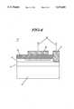
- FIG. 1is a cross-sectional view of a voltage variable capacitor in accordance with the present invention.
- FIG. 2is a graph of capacitance versus voltage at 20 KHz (FIG. 2a) and at 1 MHz (FIG. 2b) for devices in accordance with the present invention.
- FIG. 3is an isometric view of a voltage variable capacitor in an integrated circuit in accordance with the present invention.
- FIG. 4is another embodiment of the present invention.
- FIG. 5is a block diagram of a communication device incorporating the voltage variable capacitor in accordance with the invention.
- a voltage variable capacitor or varactoris a semiconductor device characterized by voltage sensitive capacitance which resides in the space-charge region at the surface of a semiconductor bounded by an insulating layer. Varactors are also known as varactor diodes, variable capacitance diodes, varicaps and voltage variable capacitors (VVC's).
- VVCvoltage variable capacitors
- a depletion layeris a region of net space-charge in a semiconductor in which the density of mobile charge carriers is much less than the density of ionized impurity atoms. The mobile carrier charge density is insufficient to neutralize the fixed charged density of donors and acceptors.
- the depletion layeris also known as a barrier layer, a blocking layer, or a space-charged layer.
- a Metal-Insulator-Semiconductor (MIS) capacitoris formed, in which the relative dielectric constant of the insulator is much larger than the relative dielectric constant of the semiconductor depletion layer.
- the semiconductoritself is typically single crystal silicon, but may be other materials common to the art.
- the semiconductormay be heavily doped except for a high resistivity surface layer which is less heavily doped.
- the surface layerhas a higher resistivity than the semiconductor substrate and may be a single crystal layer of silicon that is epitaxially grown on the semiconductor. It may also be a polysilicon layer or be counter-doped in comparison to the semiconductor.
- a voltage variable capacitor 10is formed on a semiconductor 12.
- the surface layer 14, which is less heavily doped,has a higher resistivity than the semiconductor and serves as an area for the depletion layer to form.
- An insulator layer 16is applied over the surface layer 14.
- the insulator layer 16is preferably zirconium titanate (ZrTiO 4 ) applied in a thickness from 300 ⁇ ngstroms to 1000 ⁇ ngstroms, but thicknesses from 100 ⁇ ngstroms to 2 microns have been found to be suitable.
- the material employed as the dielectric or insulating layershould have a dielectric constant much greater than that of the semiconductor. Examples of suitable materials that may be used for this purpose are to be found in TABLE 1 below:
- Oxides of additional elements such as molybdenum, tungsten and vanadiummay also be expected to be useful, either alone or in combination with other elements.
- a space-charge or depletion layer 20When an appropriate reverse bias 13 is applied to a metal electrode 18, mobile minority charge carriers are attached to a semiconductor insulator interface 19, forming a space-charge or depletion layer 20, which extends for some distance into the conductor 14.
- This depletion layerbehaves as a variable width capacitor which is electrically in series with the capacitor formed by the insulator layer 16. These two series capacitors serve to create a net capacitance effect that is affected by the changes of each individual capacitor.
- the electrode bias voltagecontrols the width of the depletion layer from zero at the accumulation threshold to a maximum thickness at the inversion threshold and thereby varies the total capacitance of the device.
- the insulator layer 16serves to provide the spacing between the top electrode 18 and the depletion layer 20.
- the depletion layeris a transient layer formed when the bias voltage is applied to the capacitor through inputs 13 and 15.
- the layer 20may be reduced in size or disappear when the applied voltage field is varied or removed. Although shown in the drawing as a distinct feature, the depletion layer 20 should not be regarded as a permanent mechanical feature of the device 10.
- the operation theory described hereinis similar to that found in operation of metal-oxide-semiconductor capacitors.
- the inversion threshold voltageAt the inversion threshold voltage, enough charge carriers have been attracted to the semiconductor interface such that an inversion layer is formed.
- Increasing the voltage biasincreases the width of the inversion layer, until the layer reaches a maximum width, beyond which the depletion layer cannot be substantially increased by increasing electrode bias voltage.
- the maximum depletion widthis determined by the concentration of the impurity dopant near the semiconductor surface onto which the insulator layer 16 has been deposited.
- Dopantssuch as phosphorous, antimony, boron and arsenic will be recognized by those skilled in the art to be useful with silicon substrates.
- Other semiconductor substrates, such as gallium arsenidemay also be utilized to form a VVC in accordance with the invention.
- the thickness of a less heavily doped surface layermay be chosen to be equal to or slightly greater than this maximum depletion width in order to minimize the series resistance of the device while maximizing the capacitance change.
- Formation of an improved voltage variable capacitoris highly dependent upon the choice of the material comprising the insulator layer 16.
- a material with a much larger relative dielectric constant than the semiconductor depletion layer 20By choosing a material with a much larger relative dielectric constant than the semiconductor depletion layer 20, a larger ratio of maximum-to-minimum capacitance will be obtained.
- the ratio of maximum-to-minimum capacitance for a MIS capacitoris given by: ##EQU1## Where C max is the maximum capacitance, C min is the minimum capacitance, K ins is the relative dielectric constant of the insulator, W d is the width of the depletion layer, K d is the relative dielectric constant of the depletion layer, and W ins is the thickness of the insulating layer.
- ferroelectric materialswith very high dielectric constants have ferroelectric properties which are not desirable for high frequency devices.
- the polarization for a ferroelectric materialhas a hysteresis loop, or memory, whereby a residue polarization remains after an applied bias voltage has been removed.
- a residual depletion layerwould also remain and thereby limit the capacitance ratio which may be obtained.
- a low-loss, non-ferroelectric insulator layeris required for high frequency applications, specifically those for use in radio transmitting and receiving, and especially for tunable high-Q filters.
- Zirconium Titanate (ZrTiO 4 )is one suitable non-ferroelectric material with a high relative dielectric constant (K r is approximately equal to 40) and low dielectric loss.
- K ris approximately equal to 40
- the relative dielectric constant of silicon dioxideused in conventional MOS capacitors
- the dielectric constant of the depletion layer in siliconis 11.7 and the dielectric constant of the depletion layer in germanium is 15.7.
- the dielectric constant of the zirconium titanate and the aforementioned materials in Table 1is much larger than that of silicon dioxide, therefore an improved capacitor having higher capacitance ratio can be fabricated.
- Thin films of zirconium titanatecan be formed by any of several techniques, including but not necessarily limited to, sputtering, evaporation, chemical vapor deposition, ion beam or plasma enhanced processes, sol-gel, and other solution chemistry processes.
- the depletion layerhas the same dielectric constant throughout and a depletion width that is controlled by the reverse bias voltage.
- the maximum width of this depletion layer capacitoris ultimately limited by the avalanche breakdown, which is also dependent on dopant concentration. In practice, however, these breakdown voltages are quite large and the maximum achievable depletion width is determined by the magnitude of the available bias voltage, typically ten volts or less for portable radio applications.
- the high dielectric constant, thin film capacitorrequires a smaller bias control voltage than the varactor diode (0.5 to 3.0 volts for zirconium titanate) depending upon the insulator film thickness and the semiconductor doping, and it has lower leakage than a varator diode.
- the high K thin film MIS capacitorsmay be used in both bi-polar and MOS processes, whereas high-performance varactor diodes are not compatible with the MOS processes.
- FIG. 3a cut-away isometric view of a voltage-variable capacitor. Electrode 11 is used to provide electrical connection with the silicion substrate 12 and ultimately to the epitaxial layer 14 in order to form the depletion layer 20.
- An alternate embodiment of the inventionis shown in FIG. 4, wherein an additional very thin layer 17 of doped material is used in addition to the conventional epitaxial layer. This very thin layer may also be made from polysilicon. Electrical contact to the thin layer is made through electrode 11 by electrically connecting the outputs 13 of the device. Obviously, such a capacitor as described herein may be easily incorporated into an integrated circuit.
- Radiosutilize resonator networks or circuits that may be turned by a voltage variable capacitor, and those operating at high frequencies realize significant advantages from a voltage variable capacitor that has low loss, high Q, and large capacitance range.
- FIG. 5a block diagram of the electrical components of the radio or communication device 50 is shown.
- the radio 50includes a demodulator 56 coupled to the antenna 62 via a filter(s) 60.
- the operation of the radio 50is controlled by a controller 54 which includes the memory block 52.
- the controller 54communicates to the demodulator 56 and controls the audio circuit block 58.
- the demodulated signal from the demodulator 56is coupled to a speaker 64 via the audio circuit 58.
- the combination of the memory block 52, the controller 54, demodulator 56, and the filter 60constitutes a receiver means in the communication device 50.
- the voltage variable capacitors as described hereinwill preferably find application in the filter 60, but may also be utilized in the demodulater 56 and/or the audio circuits 58.
Landscapes
- Engineering & Computer Science (AREA)
- Power Engineering (AREA)
- Microelectronics & Electronic Packaging (AREA)
- Semiconductor Integrated Circuits (AREA)
Abstract
Description
This invention relates generally to capacitors, and more specifically to voltage variable capacitors, also known as varactors.
High quality, precisely controlled capacitors are an integral part of many semiconductor devices. Capacitors are fabricated as part of a semiconductor circuit by using the Metal Oxide Silicon (MOS) system. One particular use of semiconductor capacitors is in an integrated circuit whose function is the conversion of analog signals to digital representation. The analog-to-digital conversion is accomplished by a sequential comparison of a signal with fractions of a reference voltage. The reference is divided by applying the comparison through an array of capacitors having capacitances that are successively reduced by factors of two. For an analog-to-digital conversion circuit to function properly, the capacitors in the circuit must be precisely controlled over the entire capacitance value of the circuit. This is accomplished by placing an oxide, such as silicon oxide, over the semiconductor and then fabricating an electrode over the oxide in order to form the capacitor.
Another use for semiconductor capacitors is in applications requiring voltage variable capacitors (VVC) also known as varactors. Currently, varactors are used as voltage variable capacitors to tune the center frequency of electrical networks consisting of resistors, inductors, and capacitors. Varactors with large capacitance per unit area, large capacitance change, and low DC leakage currents are necessary to increase the dynamic range and efficiency of tuned resonators while using lower control voltages. In order to achieve these requirements, high performance VVC's must be used as discrete components in a hybrid package because the currently available high performance VVC's are not compatible with the MOS fabrication process. The performance of the varactor is limited by the electrical characteristics of the insulator, silicon oxide, used in conventional art VVC's. In order to achieve the necessary performance increase, an increased capacitance range must be realized. It would be highly advantageous if the dielectric material would be compatible with the MOS processing and also with bipolar processing schemes.
Briefly, according to the invention, there is provided a voltage variable capacitor. The capacitor has as the base substrate a silicon wafer with a layer of high resistivity semiconductor material on top of the substrate. An insulating layer of a metal oxide having a dielectric constant greater than the dielectric constant of the semiconductor is formed on top of the high resistivity layer, and a metal electrode is formed on the insulating layer. When the electrode is suitably energized, a depletion layer can be formed in the high resistivity layer.
FIG. 1 is a cross-sectional view of a voltage variable capacitor in accordance with the present invention.
FIG. 2 is a graph of capacitance versus voltage at 20 KHz (FIG. 2a) and at 1 MHz (FIG. 2b) for devices in accordance with the present invention.
FIG. 3 is an isometric view of a voltage variable capacitor in an integrated circuit in accordance with the present invention.
FIG. 4 is another embodiment of the present invention.
FIG. 5 is a block diagram of a communication device incorporating the voltage variable capacitor in accordance with the invention.
A voltage variable capacitor or varactor is a semiconductor device characterized by voltage sensitive capacitance which resides in the space-charge region at the surface of a semiconductor bounded by an insulating layer. Varactors are also known as varactor diodes, variable capacitance diodes, varicaps and voltage variable capacitors (VVC's). In order for a VVC to function, a depletion layer must be formed. A depletion layer is a region of net space-charge in a semiconductor in which the density of mobile charge carriers is much less than the density of ionized impurity atoms. The mobile carrier charge density is insufficient to neutralize the fixed charged density of donors and acceptors. The depletion layer is also known as a barrier layer, a blocking layer, or a space-charged layer.
In order to fabricate an improved voltage variable capacitor with larger capacitance and lower DC leakage current, a novel arrangement of materials is necessary. A Metal-Insulator-Semiconductor (MIS) capacitor is formed, in which the relative dielectric constant of the insulator is much larger than the relative dielectric constant of the semiconductor depletion layer. The semiconductor itself is typically single crystal silicon, but may be other materials common to the art. The semiconductor may be heavily doped except for a high resistivity surface layer which is less heavily doped. The surface layer has a higher resistivity than the semiconductor substrate and may be a single crystal layer of silicon that is epitaxially grown on the semiconductor. It may also be a polysilicon layer or be counter-doped in comparison to the semiconductor.
Referring now to FIG. 1, avoltage variable capacitor 10 is formed on asemiconductor 12. Thesurface layer 14, which is less heavily doped, has a higher resistivity than the semiconductor and serves as an area for the depletion layer to form. Aninsulator layer 16 is applied over thesurface layer 14. Theinsulator layer 16 is preferably zirconium titanate (ZrTiO4) applied in a thickness from 300 Ångstroms to 1000 Ångstroms, but thicknesses from 100 Ångstroms to 2 microns have been found to be suitable. The material employed as the dielectric or insulating layer should have a dielectric constant much greater than that of the semiconductor. Examples of suitable materials that may be used for this purpose are to be found in TABLE 1 below:
TABLE 1 ______________________________________ tantalum pentoxide Ta.sub.2 O.sub.5 niobium pentoxide Nb.sub.2 O.sub.5 zirconium oxide ZrO.sub.2 titanium dioxide TiO.sub.2 zirconium titanate ZrTiO.sub.4 strontium titanate SrTiO.sub.3 barium titanate BaTiO.sub.3 lead titanate PbTiO.sub.3 barium tetratitanate Ba.sub.2 Ti.sub.9 O.sub.20 barium neodymium titanate BaNd.sub.2 Ti.sub.5 O.sub.14 lead-zirconium titanate Pb(Zr,Ti)O.sub.3 lead-lanthanum zirconium titanate (Pb,La)(Zr,Ti)O.sub.3 lithium niobate LiNbO.sub.3 strontium-baruim niobate (Sr,Ba)Nb.sub.2 O.sub.6 ______________________________________
Oxides of additional elements such as molybdenum, tungsten and vanadium may also be expected to be useful, either alone or in combination with other elements.
When an appropriatereverse bias 13 is applied to ametal electrode 18, mobile minority charge carriers are attached to asemiconductor insulator interface 19, forming a space-charge ordepletion layer 20, which extends for some distance into theconductor 14. This depletion layer behaves as a variable width capacitor which is electrically in series with the capacitor formed by theinsulator layer 16. These two series capacitors serve to create a net capacitance effect that is affected by the changes of each individual capacitor. The electrode bias voltage controls the width of the depletion layer from zero at the accumulation threshold to a maximum thickness at the inversion threshold and thereby varies the total capacitance of the device. Theinsulator layer 16 serves to provide the spacing between thetop electrode 18 and thedepletion layer 20. The depletion layer is a transient layer formed when the bias voltage is applied to the capacitor throughinputs layer 20 may be reduced in size or disappear when the applied voltage field is varied or removed. Although shown in the drawing as a distinct feature, thedepletion layer 20 should not be regarded as a permanent mechanical feature of thedevice 10. The operation theory described herein is similar to that found in operation of metal-oxide-semiconductor capacitors.
At the inversion threshold voltage, enough charge carriers have been attracted to the semiconductor interface such that an inversion layer is formed. Increasing the voltage bias increases the width of the inversion layer, until the layer reaches a maximum width, beyond which the depletion layer cannot be substantially increased by increasing electrode bias voltage. The maximum depletion width is determined by the concentration of the impurity dopant near the semiconductor surface onto which theinsulator layer 16 has been deposited. Dopants such as phosphorous, antimony, boron and arsenic will be recognized by those skilled in the art to be useful with silicon substrates. Other semiconductor substrates, such as gallium arsenide, may also be utilized to form a VVC in accordance with the invention.
The lower the doping, the larger the maximum depletion layer thickness, and thus, the lower minimum capacitance which can be achieved. The thickness of a less heavily doped surface layer may be chosen to be equal to or slightly greater than this maximum depletion width in order to minimize the series resistance of the device while maximizing the capacitance change.
Formation of an improved voltage variable capacitor is highly dependent upon the choice of the material comprising theinsulator layer 16. By choosing a material with a much larger relative dielectric constant than thesemiconductor depletion layer 20, a larger ratio of maximum-to-minimum capacitance will be obtained. The larger the insulator's dielectric constant, the larger the capacitance ratio in capacitance per unit area will be for a given insulator thickness. The ratio of maximum-to-minimum capacitance for a MIS capacitor is given by: ##EQU1## Where Cmax is the maximum capacitance, Cmin is the minimum capacitance, Kins is the relative dielectric constant of the insulator, Wd is the width of the depletion layer, Kd is the relative dielectric constant of the depletion layer, and Wins is the thickness of the insulating layer.
Many materials with very high dielectric constants have ferroelectric properties which are not desirable for high frequency devices. The polarization for a ferroelectric material has a hysteresis loop, or memory, whereby a residue polarization remains after an applied bias voltage has been removed. Thus, a residual depletion layer would also remain and thereby limit the capacitance ratio which may be obtained. These materials would be best utilized in lower frequency applications.
A low-loss, non-ferroelectric insulator layer is required for high frequency applications, specifically those for use in radio transmitting and receiving, and especially for tunable high-Q filters. Zirconium Titanate (ZrTiO4) is one suitable non-ferroelectric material with a high relative dielectric constant (Kr is approximately equal to 40) and low dielectric loss. By comparison, the relative dielectric constant of silicon dioxide (used in conventional MOS capacitors) is 3.9. The dielectric constant of the depletion layer in silicon is 11.7 and the dielectric constant of the depletion layer in germanium is 15.7. It can be easily seen that the dielectric constant of the zirconium titanate and the aforementioned materials in Table 1 is much larger than that of silicon dioxide, therefore an improved capacitor having higher capacitance ratio can be fabricated. Thin films of zirconium titanate can be formed by any of several techniques, including but not necessarily limited to, sputtering, evaporation, chemical vapor deposition, ion beam or plasma enhanced processes, sol-gel, and other solution chemistry processes.
By choosing an insulator with a much larger relative dielectric constant than a semiconductor depletion layer, a larger ratio between the maximum capacitance at zero depletion layer thickness and the minimum capacitance at the inversion threshold can be achieved. This strategy has been largely overlooked because the theory of MIS capacitors was developed with a silicon dioxide insulator on silicon. Because the maximum width of the depletion layer in an MIS capacitor is limited by the formation of an inversion layer, the capacitance change which can be achieved with a low dielectric constant material, such as silicon dioxide, is less than or comparable to what can be achieved by varying the depletion width around a PN junction.
In the case of a PN junction, the depletion layer has the same dielectric constant throughout and a depletion width that is controlled by the reverse bias voltage. The maximum width of this depletion layer capacitor is ultimately limited by the avalanche breakdown, which is also dependent on dopant concentration. In practice, however, these breakdown voltages are quite large and the maximum achievable depletion width is determined by the magnitude of the available bias voltage, typically ten volts or less for portable radio applications. The high dielectric constant, thin film capacitor requires a smaller bias control voltage than the varactor diode (0.5 to 3.0 volts for zirconium titanate) depending upon the insulator film thickness and the semiconductor doping, and it has lower leakage than a varator diode. The high K thin film MIS capacitors may be used in both bi-polar and MOS processes, whereas high-performance varactor diodes are not compatible with the MOS processes.
Referring now to FIG. 2, it may be seen that a very large capacitance change is noted over a small voltage range when a voltage variable capacitor is made using zirconium titanate as the insulating layer. A four-fold improvement has been made over the prior art. The current-voltage change is more linear than that observed in current varactors.
For help in understanding the structure of the aforementioned embodiments, the reader is referred to FIG. 3, a cut-away isometric view of a voltage-variable capacitor.Electrode 11 is used to provide electrical connection with thesilicion substrate 12 and ultimately to theepitaxial layer 14 in order to form thedepletion layer 20. An alternate embodiment of the invention is shown in FIG. 4, wherein an additional verythin layer 17 of doped material is used in addition to the conventional epitaxial layer. This very thin layer may also be made from polysilicon. Electrical contact to the thin layer is made throughelectrode 11 by electrically connecting theoutputs 13 of the device. Obviously, such a capacitor as described herein may be easily incorporated into an integrated circuit.
Applications requiring voltage variable capacitors that function at high frequencies, such as radio frequency communications equipment, will find particular use for a device as described herein. Radios utilize resonator networks or circuits that may be turned by a voltage variable capacitor, and those operating at high frequencies realize significant advantages from a voltage variable capacitor that has low loss, high Q, and large capacitance range. Referring to FIG. 5, a block diagram of the electrical components of the radio orcommunication device 50 is shown. Theradio 50 includes ademodulator 56 coupled to theantenna 62 via a filter(s) 60. The operation of theradio 50 is controlled by acontroller 54 which includes thememory block 52. Thecontroller 54 communicates to thedemodulator 56 and controls theaudio circuit block 58. The demodulated signal from thedemodulator 56 is coupled to aspeaker 64 via theaudio circuit 58. The combination of thememory block 52, thecontroller 54,demodulator 56, and thefilter 60 constitutes a receiver means in thecommunication device 50. The voltage variable capacitors as described herein will preferably find application in thefilter 60, but may also be utilized in thedemodulater 56 and/or theaudio circuits 58.
In summary, it may be seen that an improved voltage variable capacitor is attained by the use of insulator layer such as zirconium titanate having a high dielectric constant. The foregoing examples are intended to serve as an illustration of the preferred embodiment of the invention. Accordingly, it is not intended that the invention be limited except as by the appended claims herein.
Claims (16)
1. A voltage variable capacitor, comprising:
a semiconductor having a layer of semiconductive material of a higher resistivity than the semiconductor;
a depletion layer formed in the high resistivity layer;
an insulating layer formed on the high resistivity layer, said insulating layer being a metal oxide having a dielectric constant greater than the dielectric constant of the semiconductor; and
an conductive electrode formed on the dielectric layer.
2. A voltage variable capacitor, comprising:
a semiconductor having a layer of semiconductive material of a higher resistivity than the semiconductor;
a depletion layer formed in the high resistivity layer;
an insulating layer formed on the high resistivity layer, wherein said insulating layer is a metal oxide compound wherein the metal comprises at least first and second components selected from the group consisting of barium, lead, lithium, molybdenum, neodymium, niobium, strontium, tantalum, titanium, tungsten, vanadium, and zirconium, the insulating layer having a dielectric constant greater than the dielectric constant of the semiconductor; and
a conductive electrode formed on the insulating layer.
3. A voltage variable capacitor, comprising:
a semiconductor having a layer of semiconductive material of a higher resistivity than the semiconductor;
a depletion layer formed in the high resistivity layer;
an insulating layer formed on the high resistivity layer, wherein said insulating layer is an oxide selected from the group consisting of oxides of barium, lead, lithium, molybdenum, neodymium, niobium, strontium, tantalum, titanium, tungsten, vanadium, and zirconium, the insulating layer having a dielectric constant greater than the dielectric constant of the semiconductor; and
a conductive electrode formed on the insulating layer.
4. The voltage variable capacitor as described in claim 1, wherein the insulating layer comprises zirconium titanate.
5. The voltage variable capacitor as described in claim 1, wherein the insulating layer has a dielectric constant greater than 16.
6. The voltage variable capacitor as described in claim 1, wherein the insulating layer further comprises a low-loss, non-ferroelectric insulator.
7. The voltage variable capacitor as described in claim 1, wherein the dielectric constant of the insulating layer is greater than the dielectric constant of the high resistivity semiconductor material.
8. An integrated circuit having a voltage variable capacitor, said circuit comprising:
a semiconductor having a layer of semiconductive material of a higher resistivity than the semiconductor;
a depletion layer formed in the high resistivity layer;
an insulating layer formed on the high resistivity layer, said insulating layer being a metal oxide having a dielectric constant greater than the dielectric constant of the semiconductor; and
a conductive electrode formed on the insulating layer.
9. A voltage variable thin film capacitor, comprising;
a semiconductor having a layer of a high resistivity semiconductive material thereon;
an insulating layer formed on the high resistivity layer, comprising:
a thin film of zirconium titanate;
a metal electrode formed on the zirconium titanate; and
a depletion layer formed in the high resistivity layer upon electrically energizing the capacitor.
10. An insulating layer for a voltage variable capacitor, comprising a low-loss non-ferroelectric material having a dielectric constant equal to or greater than 40.
11. An insulating layer for a voltage variable capacitor, comprising a low-loss non-ferroelectric material having a dielectric constant equal to or greater than 40, wherein the insulating layer is a metal oxide wherein the metal comprises at least first and second components selected from the group consisting of barium, lead, lithium, molybdenum, neodymium, niobium, strontium, tantalum, titanium, tungsten, vanadium, and zirconium.
12. An insulating layer for a voltage variable capacitor, comprising a low-loss non-ferroelectric material having a dielectric constant equal to or greater than 40, wherein the insulating layer is an oxide selected from the group consisting of oxides of barium, lead, lithium, molybdenum, neodymium, niobium, strontium, tantalum, titanium, tungsten, vanadium, and zirconium.
13. The insulating layer as defined in claim 10, wherein the material comprises zirconium titanate.
14. A method of making a voltage variable capacitor, comprising the steps of:
depositing a high resistivity layer of semiconductive material on a semiconductor having the same conductivity type;
depositing a layer of a metal oxide, metal titanate or metal niobate insulating material having a dielectric constant greater than that of the semiconductor on the surface of the high resistivity layer;
forming an electrode on the insulating material; and
applying a voltage to the electrode in order to form a depletion layer in the high resistivity layer.
15. The method according to claim 14, wherein the step of coating comprises coating by sputtering, evaporation, chemical vapor deposition, ion beam, plasma, sol-gel, or solution chemistry processes.
16. A radio having a resonator, said resonator comprising: at least one voltage variable capacitor comprising:
a semiconductor substrate having a layer of a high resistivity semiconductive material thereon;
a depletion layer formed in the high resistivity layer;
an insulating layer formed on the high resistivity layer, comprising a thin film of zirconium titanate; and
an electrode formed on the zirconium titanate in an area directly above the depletion layer.
Priority Applications (8)
| Application Number | Priority Date | Filing Date | Title |
|---|---|---|---|
| US07/776,111US5173835A (en) | 1991-10-15 | 1991-10-15 | Voltage variable capacitor |
| KR1019940701230AKR0134980B1 (en) | 1991-10-15 | 1992-10-15 | Voltage variable capacitor |
| DE69232740TDE69232740T2 (en) | 1991-10-15 | 1992-10-15 | VOLTAGE VARIABLE CAPACITOR |
| JP5507787AJP2853332B2 (en) | 1991-10-15 | 1992-10-15 | Variable voltage capacitor |
| KR1019940701230AKR940703070A (en) | 1991-10-15 | 1992-10-15 | Voltage variable capacitor |
| EP92923202AEP0608376B1 (en) | 1991-10-15 | 1992-10-15 | Voltage variable capacitor |
| ES92923202TES2181679T3 (en) | 1991-10-15 | 1992-10-15 | VARIABLE CONDENSER WITH VOLTAGE. |
| PCT/US1992/008781WO1993008578A1 (en) | 1991-10-15 | 1992-10-15 | Voltage variable capacitor |
Applications Claiming Priority (1)
| Application Number | Priority Date | Filing Date | Title |
|---|---|---|---|
| US07/776,111US5173835A (en) | 1991-10-15 | 1991-10-15 | Voltage variable capacitor |
Publications (1)
| Publication Number | Publication Date |
|---|---|
| US5173835Atrue US5173835A (en) | 1992-12-22 |
Family
ID=25106486
Family Applications (1)
| Application Number | Title | Priority Date | Filing Date |
|---|---|---|---|
| US07/776,111Expired - Fee RelatedUS5173835A (en) | 1991-10-15 | 1991-10-15 | Voltage variable capacitor |
Country Status (7)
| Country | Link |
|---|---|
| US (1) | US5173835A (en) |
| EP (1) | EP0608376B1 (en) |
| JP (1) | JP2853332B2 (en) |
| KR (2) | KR940703070A (en) |
| DE (1) | DE69232740T2 (en) |
| ES (1) | ES2181679T3 (en) |
| WO (1) | WO1993008578A1 (en) |
Cited By (119)
| Publication number | Priority date | Publication date | Assignee | Title |
|---|---|---|---|---|
| US5379008A (en)* | 1993-03-03 | 1995-01-03 | Motorola, Inc. | Variable impedance circuit providing reduced distortion |
| US5390072A (en)* | 1992-09-17 | 1995-02-14 | Research Foundation Of State University Of New York | Thin film capacitors |
| US5393352A (en)* | 1992-05-01 | 1995-02-28 | Texas Instruments Incorporated | Pb/Bi-containing high-dielectric constant oxides using a non-P/Bi-containing perovskite as a buffer layer |
| US5405790A (en)* | 1993-11-23 | 1995-04-11 | Motorola, Inc. | Method of forming a semiconductor structure having MOS, bipolar, and varactor devices |
| US5493715A (en)* | 1994-08-01 | 1996-02-20 | Motorola, Inc. | Multi-range voltage controlled resonant circuit |
| US5495208A (en)* | 1994-04-04 | 1996-02-27 | Motorola, Inc. | Wide band tunable and modulatable reference oscillator |
| US5587870A (en)* | 1992-09-17 | 1996-12-24 | Research Foundation Of State University Of New York | Nanocrystalline layer thin film capacitors |
| US5600187A (en)* | 1994-06-27 | 1997-02-04 | General Electric Company | Electronically controllable capacitors using power MOSFET's |
| US5602052A (en)* | 1995-04-24 | 1997-02-11 | Harris Corporation | Method of forming dummy island capacitor |
| US5615096A (en)* | 1994-06-06 | 1997-03-25 | Motorola, Inc. | Direct current power supply conditioning circuit |
| US5673001A (en)* | 1995-06-07 | 1997-09-30 | Motorola, Inc. | Method and apparatus for amplifying a signal |
| US5688724A (en)* | 1992-07-02 | 1997-11-18 | National Semiconductor Corporation | Method of providing a dielectric structure for semiconductor devices |
| US5744385A (en)* | 1997-03-21 | 1998-04-28 | Plato Labs, Inc. | Compensation technique for parasitic capacitance |
| US5751034A (en)* | 1996-02-08 | 1998-05-12 | Symetrix Corporation | High dielectric constant barium-strontium-niobium oxides for integrated circuit applications |
| WO1998020606A3 (en)* | 1996-10-25 | 1998-06-25 | Superconducting Core Technolog | Tunable dielectric flip chip varactors |
| WO1999023705A1 (en)* | 1997-10-30 | 1999-05-14 | Fraunhofer-Gesellschaft zur Förderung der angewandten Forschung e.V. | Passive hf element and method for operating, producing and determining characteristic properties of the same |
| US5933316A (en)* | 1993-08-02 | 1999-08-03 | Motorola Inc. | Method for forming a titanate thin film on silicon, and device formed thereby |
| US5959515A (en)* | 1997-08-11 | 1999-09-28 | Motorola, Inc. | High Q integrated resonator structure |
| US5965912A (en)* | 1997-09-03 | 1999-10-12 | Motorola, Inc. | Variable capacitor and method for fabricating the same |
| US6013553A (en)* | 1997-07-24 | 2000-01-11 | Texas Instruments Incorporated | Zirconium and/or hafnium oxynitride gate dielectric |
| US6057203A (en)* | 1998-06-19 | 2000-05-02 | Programmable Silicon Solutions | Integrated circuit capacitor |
| US6100770A (en)* | 1997-09-11 | 2000-08-08 | Telefonaktiebolaget Lm Ericsson (Publ) | MIS transistor varactor device and oscillator using same |
| WO2000057454A3 (en)* | 1999-03-19 | 2001-01-18 | Ericsson Telefon Ab L M | Improved integrated oscillators and tuning circuits |
| US6190987B1 (en)* | 1996-07-22 | 2001-02-20 | Nec Corporation | MOS semiconductor device and method of manufacturing the same |
| WO2001088967A1 (en)* | 2000-05-16 | 2001-11-22 | Telefonaktiebolaget Lm Ericsson (Publ) | High-q tank |
| US6504443B1 (en) | 2000-05-17 | 2003-01-07 | Nec America, Inc., | Common anode varactor tuned LC circuit |
| US6507476B1 (en)* | 1999-11-01 | 2003-01-14 | International Business Machines Corporation | Tuneable ferroelectric decoupling capacitor |
| US6521939B1 (en) | 2000-09-29 | 2003-02-18 | Chartered Semiconductor Manufacturing Ltd. | High performance integrated varactor on silicon |
| US20030058022A1 (en)* | 1999-12-14 | 2003-03-27 | Rajendran Nair | Device and method for controlling voltage variation |
| US6541814B1 (en) | 2001-11-06 | 2003-04-01 | Pericom Semiconductor Corp. | MOS variable capacitor with controlled dC/dV and voltage drop across W of gate |
| US20030155658A1 (en)* | 2000-12-21 | 2003-08-21 | Ioffe Valery Moiseevich | Semiconductor device |
| US20030178620A1 (en)* | 2000-09-11 | 2003-09-25 | Adolf Bernds | Organic rectifier, circuit, rfid tag and use of an organic rectifier |
| US6638838B1 (en) | 2000-10-02 | 2003-10-28 | Motorola, Inc. | Semiconductor structure including a partially annealed layer and method of forming the same |
| US6639249B2 (en) | 2001-08-06 | 2003-10-28 | Motorola, Inc. | Structure and method for fabrication for a solid-state lighting device |
| EP1113498A3 (en)* | 1999-12-29 | 2003-10-29 | Motorola, Inc. | Voltage variable capacitor with improved c-v linearity |
| US6646293B2 (en) | 2001-07-18 | 2003-11-11 | Motorola, Inc. | Structure for fabricating high electron mobility transistors utilizing the formation of complaint substrates |
| US6667196B2 (en) | 2001-07-25 | 2003-12-23 | Motorola, Inc. | Method for real-time monitoring and controlling perovskite oxide film growth and semiconductor structure formed using the method |
| US6667539B2 (en) | 2001-11-08 | 2003-12-23 | International Business Machines Corporation | Method to increase the tuning voltage range of MOS varactors |
| US6673667B2 (en) | 2001-08-15 | 2004-01-06 | Motorola, Inc. | Method for manufacturing a substantially integral monolithic apparatus including a plurality of semiconductor materials |
| US6673646B2 (en) | 2001-02-28 | 2004-01-06 | Motorola, Inc. | Growth of compound semiconductor structures on patterned oxide films and process for fabricating same |
| US6686817B2 (en) | 2000-12-12 | 2004-02-03 | Paratek Microwave, Inc. | Electronic tunable filters with dielectric varactors |
| US20040029310A1 (en)* | 2000-08-18 | 2004-02-12 | Adoft Bernds | Organic field-effect transistor (ofet), a production method therefor, an integrated circut constructed from the same and their uses |
| US20040026121A1 (en)* | 2000-09-22 | 2004-02-12 | Adolf Bernds | Electrode and/or conductor track for organic components and production method thereof |
| US20040026689A1 (en)* | 2000-08-18 | 2004-02-12 | Adolf Bernds | Encapsulated organic-electronic component, method for producing the same and use thereof |
| US6693033B2 (en) | 2000-02-10 | 2004-02-17 | Motorola, Inc. | Method of removing an amorphous oxide from a monocrystalline surface |
| US6693298B2 (en) | 2001-07-20 | 2004-02-17 | Motorola, Inc. | Structure and method for fabricating epitaxial semiconductor on insulator (SOI) structures and devices utilizing the formation of a compliant substrate for materials used to form same |
| US6709989B2 (en) | 2001-06-21 | 2004-03-23 | Motorola, Inc. | Method for fabricating a semiconductor structure including a metal oxide interface with silicon |
| US20040056137A1 (en)* | 2000-12-08 | 2004-03-25 | Bernhard Bocht | Device for drawing up card clothing |
| US20040062294A1 (en)* | 2000-12-08 | 2004-04-01 | Wolfgang Clemens | Device for detecting and/or transmitting at least one environmental influence, method for producing said device and use thereof |
| US20040094771A1 (en)* | 2001-03-26 | 2004-05-20 | Adolf Bernds | Device with at least two organic electronic components and method for producing the same |
| US20040158728A1 (en)* | 2003-02-06 | 2004-08-12 | Seo-Kyu Kim | Smart cards having protection circuits therein that inhibit power analysis attacks and methods of operating same |
| US20040209191A1 (en)* | 2001-06-01 | 2004-10-21 | Adolf Bernds | Method for producing conductive structures by means of printing technique, and active components produced therefrom for integrated circuits |
| US20040219460A1 (en)* | 2001-02-09 | 2004-11-04 | Adolf Bernds | Organic field effect transistor with a photostructured gate dielectric, method for the production and use thereof in organic electronics |
| US20040217444A1 (en)* | 2001-10-17 | 2004-11-04 | Motorola, Inc. | Method and apparatus utilizing monocrystalline insulator |
| US6828638B2 (en) | 1999-12-22 | 2004-12-07 | Intel Corporation | Decoupling capacitors for thin gate oxides |
| US20040256467A1 (en)* | 2001-10-18 | 2004-12-23 | Wolfgang Clemens | Electronic unit, circuit design for the same, and production method |
| US20040262599A1 (en)* | 2001-06-01 | 2004-12-30 | Adolf Bernds | Organic field effect transistor, method for production and use thereof in the assembly of integrated circuits |
| US20050000647A1 (en)* | 2001-11-19 | 2005-01-06 | Tatsuo Matsumoto | Method and facility for separating and recovering steel pipe and covering resin in resin-covered steel pipe |
| US6841439B1 (en)* | 1997-07-24 | 2005-01-11 | Texas Instruments Incorporated | High permittivity silicate gate dielectric |
| US6855992B2 (en) | 2001-07-24 | 2005-02-15 | Motorola Inc. | Structure and method for fabricating configurable transistor devices utilizing the formation of a compliant substrate for materials used to form the same |
| WO2005020257A3 (en)* | 2003-08-20 | 2005-04-14 | Polyic Gmbh & Co Kg | Organic capacitor having a voltage-controlled capacitance |
| US6885065B2 (en) | 2002-11-20 | 2005-04-26 | Freescale Semiconductor, Inc. | Ferromagnetic semiconductor structure and method for forming the same |
| US20050106507A1 (en)* | 2002-03-21 | 2005-05-19 | Adolf Bernds | Device and method for laser structuring functional polymers and the use thereof |
| US20050113138A1 (en)* | 2002-03-18 | 2005-05-26 | Greg Mendolia | RF ID tag reader utlizing a scanning antenna system and method |
| US20050112827A1 (en)* | 1997-07-24 | 2005-05-26 | Anthony John M. | High permittivity silicate gate dielectric |
| US6916717B2 (en) | 2002-05-03 | 2005-07-12 | Motorola, Inc. | Method for growing a monocrystalline oxide layer and for fabricating a semiconductor device on a monocrystalline substrate |
| US20050211972A1 (en)* | 2001-12-11 | 2005-09-29 | Siemens Aktiengesellschaft | Organic field effect transistor with off-set threshold voltage and the use thereof |
| US20050224787A1 (en)* | 2002-06-13 | 2005-10-13 | Wolfgang Clemens | Substrate for an organic field effect transistor, use of said substrate, method for increasing the charge carrier mobility, and organic field effect transistor (ofet) |
| US6965128B2 (en) | 2003-02-03 | 2005-11-15 | Freescale Semiconductor, Inc. | Structure and method for fabricating semiconductor microresonator devices |
| US20050277240A1 (en)* | 2002-03-21 | 2005-12-15 | Walter Fix | Logic components from organic field effect transistors |
| US6992321B2 (en) | 2001-07-13 | 2006-01-31 | Motorola, Inc. | Structure and method for fabricating semiconductor structures and devices utilizing piezoelectric materials |
| US20060024947A1 (en)* | 2002-07-29 | 2006-02-02 | Wolfgang Clements | Electronic component comprising predominantly organic functional materials and a method for the production thereof |
| US20060035423A1 (en)* | 2002-11-19 | 2006-02-16 | Walter Fix | Organic electronic component comprising the same organic material for at least two functional layers |
| US7005717B2 (en) | 2000-05-31 | 2006-02-28 | Freescale Semiconductor, Inc. | Semiconductor device and method |
| US20060057769A1 (en)* | 2003-01-21 | 2006-03-16 | Adolf Bernds | Use of conductive carbon black/graphite mixtures for the production of low-cost electronics |
| US7019332B2 (en) | 2001-07-20 | 2006-03-28 | Freescale Semiconductor, Inc. | Fabrication of a wavelength locker within a semiconductor structure |
| US7020374B2 (en) | 2003-02-03 | 2006-03-28 | Freescale Semiconductor, Inc. | Optical waveguide structure and method for fabricating the same |
| US20060079327A1 (en)* | 2002-08-08 | 2006-04-13 | Wolfgang Clemens | Electronic device |
| US7045815B2 (en) | 2001-04-02 | 2006-05-16 | Freescale Semiconductor, Inc. | Semiconductor structure exhibiting reduced leakage current and method of fabricating same |
| US20060118780A1 (en)* | 2003-01-09 | 2006-06-08 | Axel Gerlt | Organo-resistive memory unit |
| US20060118779A1 (en)* | 2002-11-19 | 2006-06-08 | Wolfgang Clemens | Organic Electronic Component Comprising A Patterned, Semi-Conducting Functional Layer And A Method For Producing Said Component |
| US20060118778A1 (en)* | 2002-11-05 | 2006-06-08 | Wolfgang Clemens | Organic electronic component with high-resolution structuring and method for the production thereof |
| US20060121625A1 (en)* | 2002-11-14 | 2006-06-08 | Wolfgang Clemens | Measuring apparatus used for determining an analyte in a liquid sample, comprising polymer electronic components |
| US7067856B2 (en) | 2000-02-10 | 2006-06-27 | Freescale Semiconductor, Inc. | Semiconductor structure, semiconductor device, communicating device, integrated circuit, and process for fabricating the same |
| US20060138701A1 (en)* | 2003-07-03 | 2006-06-29 | Jurgen Ficker | Method and device for structuring organic layers |
| US20060160266A1 (en)* | 2003-01-21 | 2006-07-20 | Adolf Bernds | Organic electronic component and method for producing organic electronic devices |
| US7105866B2 (en) | 2000-07-24 | 2006-09-12 | Freescale Semiconductor, Inc. | Heterojunction tunneling diodes and process for fabricating same |
| US20060220005A1 (en)* | 2003-07-03 | 2006-10-05 | Walter Fix | Logic gate with a potential-free gate electrode for organic integrated circuits |
| US7161227B2 (en) | 2001-08-14 | 2007-01-09 | Motorola, Inc. | Structure and method for fabricating semiconductor structures and devices for detecting an object |
| US20070008019A1 (en)* | 2003-09-03 | 2007-01-11 | Wolfgang Clemens | Mechanical control elements for organic polymer electronic devices |
| US20070017401A1 (en)* | 2003-09-03 | 2007-01-25 | Polyic Gmbh & Co. Kg | Polymer mixtures for printed polymer electronic circuits |
| US20070018649A1 (en)* | 2005-07-19 | 2007-01-25 | Prsha Jeffrey A | Compact self-tuned electrical resonator for buried object locator applications |
| US7169619B2 (en) | 2002-11-19 | 2007-01-30 | Freescale Semiconductor, Inc. | Method for fabricating semiconductor structures on vicinal substrates using a low temperature, low pressure, alkaline earth metal-rich process |
| US7211852B2 (en) | 2001-01-19 | 2007-05-01 | Freescale Semiconductor, Inc. | Structure and method for fabricating GaN devices utilizing the formation of a compliant substrate |
| US7229868B2 (en) | 2000-12-08 | 2007-06-12 | Polyic Gmbh & Co. Kg | Organic field-effect transistor, method for structuring an OFET and integrated circuit |
| US7298023B2 (en) | 2001-10-16 | 2007-11-20 | Polyic Gmbh & Co. Kg | Electronic device with organic insulator |
| CN100371972C (en)* | 2003-05-29 | 2008-02-27 | 三洋电机株式会社 | Pixel circuit and display device |
| US20080083969A1 (en)* | 2006-10-06 | 2008-04-10 | Semiconductor Energy Laboratory Co., Ltd. | Rectifier circuit, semiconductor device using the rectifier circuit, and driving method thereof |
| US20080143531A1 (en)* | 2006-12-18 | 2008-06-19 | Semiconductor Energy Laboratory Co., Ltd. | Semiconductor Device |
| US7414513B2 (en) | 2002-08-23 | 2008-08-19 | Polyic Gmbh & Co. Kg | Organic component for overvoltage protection and associated circuit |
| US7479670B2 (en) | 2003-08-25 | 2009-01-20 | Polyic Gmbh & Co Kg | Organic electronic component with high resolution structuring, and method of the production thereof |
| US20090046407A1 (en)* | 2007-06-08 | 2009-02-19 | Liann-Be Chang | Cascade electromagnetic pulse protection circuit |
| US20090088105A1 (en)* | 2007-09-28 | 2009-04-02 | Ahmadreza Rofougaran | Method and system for utilizing a programmable coplanar waveguide or microstrip bandpass filter for undersampling in a receiver |
| US20090128724A1 (en)* | 2007-11-21 | 2009-05-21 | Hannstar Display Corporation | Liquid crystal display |
| US20090189147A1 (en)* | 2004-01-14 | 2009-07-30 | Walter Fix | Organic transistor comprising a self-aligning gate electrode, and method for the production thereof |
| US7589553B2 (en) | 2005-03-01 | 2009-09-15 | Polyic Gmbh & Co. Kg | Electronic module with organic logic circuit elements |
| US20090310273A1 (en)* | 2008-03-21 | 2009-12-17 | Liann-Be Chang | Electromagnetic pulse protection circuit having wave filtering capability |
| US7656036B2 (en) | 2003-02-14 | 2010-02-02 | Nec Corporation | Line component and semiconductor circuit using line component |
| US7724550B2 (en) | 2004-12-23 | 2010-05-25 | Polyic Gmbh & Co. Kg | Organic rectifier |
| US7812343B2 (en) | 2005-04-15 | 2010-10-12 | Polyic Gmbh & Co. Kg | Multilayer composite body having an electronic function |
| US7843342B2 (en) | 2005-03-01 | 2010-11-30 | Polyic Gmbh & Co. Kg | Organic clock generator |
| US7846838B2 (en) | 2005-07-29 | 2010-12-07 | Polyic Gmbh & Co. Kg | Method for producing an electronic component |
| US7847695B2 (en) | 2004-08-23 | 2010-12-07 | Polyic Gmbh & Co. Kg | External package capable of being radio-tagged |
| US7940340B2 (en) | 2005-07-04 | 2011-05-10 | Polyic Gmbh & Co. Kg | Multilayer body with electrically controllable optically active systems of layers |
| US7940159B2 (en) | 2004-12-10 | 2011-05-10 | Polyic Gmbh & Co. Kg | Identification system |
| US20110169809A1 (en)* | 2005-05-03 | 2011-07-14 | Hannstar Display Corporation | Pixel Structure with Improved Viewing Angle |
| US8315061B2 (en) | 2005-09-16 | 2012-11-20 | Polyic Gmbh & Co. Kg | Electronic circuit with elongated strip layer and method for the manufacture of the same |
| US10629756B2 (en)* | 2012-09-13 | 2020-04-21 | Taiwan Semiconductor Manufacturing Co., Ltd. | Semiconductor structure |
| US20220351768A1 (en)* | 2017-05-09 | 2022-11-03 | Micron Technology, Inc. | Ferroelectric devices and ferroelectric memory cells |
Families Citing this family (5)
| Publication number | Priority date | Publication date | Assignee | Title |
|---|---|---|---|---|
| US6727535B1 (en)* | 1998-11-09 | 2004-04-27 | Paratek Microwave, Inc. | Ferroelectric varactor with built-in DC blocks |
| DE102004059464A1 (en) | 2004-12-10 | 2006-06-29 | Polyic Gmbh & Co. Kg | Electronic component with modulator |
| CN101228630B (en) | 2005-05-30 | 2011-10-05 | 株式会社半导体能源研究所 | Semiconductor device |
| JP5185845B2 (en)* | 2009-01-27 | 2013-04-17 | 株式会社神戸製鋼所 | Variable capacitance element |
| KR101067496B1 (en)* | 2009-04-08 | 2011-09-27 | 주식회사 에스세라 | Voltage varying unit and surface mount device having same |
Citations (8)
| Publication number | Priority date | Publication date | Assignee | Title |
|---|---|---|---|---|
| US3202891A (en)* | 1960-11-30 | 1965-08-24 | Gen Telephone & Elect | Voltage variable capacitor with strontium titanate dielectric |
| US3512052A (en)* | 1968-01-11 | 1970-05-12 | Gen Motors Corp | Metal-insulator-semiconductor voltage variable capacitor with controlled resistivity dielectric |
| US3634738A (en)* | 1970-10-06 | 1972-01-11 | Kev Electronics Corp | Diode having a voltage variable capacitance characteristic and method of making same |
| US3648340A (en)* | 1969-08-11 | 1972-03-14 | Gen Motors Corp | Hybrid solid-state voltage-variable tuning capacitor |
| US3809971A (en)* | 1972-03-17 | 1974-05-07 | Norton Co | Microfarad range varactor |
| US3890635A (en)* | 1973-12-26 | 1975-06-17 | Gen Electric | Variable capacitance semiconductor devices |
| US4005466A (en)* | 1975-05-07 | 1977-01-25 | Rca Corporation | Planar voltage variable tuning capacitors |
| US4782350A (en)* | 1987-10-28 | 1988-11-01 | Xerox Corporation | Amorphous silicon varactors as rf amplitude modulators and their application to acoustic ink printers |
Family Cites Families (4)
| Publication number | Priority date | Publication date | Assignee | Title |
|---|---|---|---|---|
| JPS5745968A (en)* | 1980-08-29 | 1982-03-16 | Ibm | Capacitor with double dielectric unit |
| JPS5873146A (en)* | 1981-10-28 | 1983-05-02 | Hitachi Ltd | Hybrid integrated circuit and manufacture thereof |
| JP2639041B2 (en) | 1989-01-09 | 1997-08-06 | 日本電気株式会社 | Varactor diode manufacturing method |
| US5192871A (en)* | 1991-10-15 | 1993-03-09 | Motorola, Inc. | Voltage variable capacitor having amorphous dielectric film |
- 1991
- 1991-10-15USUS07/776,111patent/US5173835A/ennot_activeExpired - Fee Related
- 1992
- 1992-10-15JPJP5507787Apatent/JP2853332B2/ennot_activeExpired - Fee Related
- 1992-10-15ESES92923202Tpatent/ES2181679T3/ennot_activeExpired - Lifetime
- 1992-10-15WOPCT/US1992/008781patent/WO1993008578A1/enactiveIP Right Grant
- 1992-10-15EPEP92923202Apatent/EP0608376B1/ennot_activeExpired - Lifetime
- 1992-10-15DEDE69232740Tpatent/DE69232740T2/ennot_activeExpired - Fee Related
- 1992-10-15KRKR1019940701230Apatent/KR940703070A/enactiveGranted
- 1992-10-15KRKR1019940701230Apatent/KR0134980B1/ennot_activeExpired - Fee Related
Patent Citations (8)
| Publication number | Priority date | Publication date | Assignee | Title |
|---|---|---|---|---|
| US3202891A (en)* | 1960-11-30 | 1965-08-24 | Gen Telephone & Elect | Voltage variable capacitor with strontium titanate dielectric |
| US3512052A (en)* | 1968-01-11 | 1970-05-12 | Gen Motors Corp | Metal-insulator-semiconductor voltage variable capacitor with controlled resistivity dielectric |
| US3648340A (en)* | 1969-08-11 | 1972-03-14 | Gen Motors Corp | Hybrid solid-state voltage-variable tuning capacitor |
| US3634738A (en)* | 1970-10-06 | 1972-01-11 | Kev Electronics Corp | Diode having a voltage variable capacitance characteristic and method of making same |
| US3809971A (en)* | 1972-03-17 | 1974-05-07 | Norton Co | Microfarad range varactor |
| US3890635A (en)* | 1973-12-26 | 1975-06-17 | Gen Electric | Variable capacitance semiconductor devices |
| US4005466A (en)* | 1975-05-07 | 1977-01-25 | Rca Corporation | Planar voltage variable tuning capacitors |
| US4782350A (en)* | 1987-10-28 | 1988-11-01 | Xerox Corporation | Amorphous silicon varactors as rf amplitude modulators and their application to acoustic ink printers |
Cited By (159)
| Publication number | Priority date | Publication date | Assignee | Title |
|---|---|---|---|---|
| US5650646A (en)* | 1992-05-01 | 1997-07-22 | Texas Instruments Incorporated | Pb/Bi-containing high-dielectric constant oxides using a non-Pb/Bi-containing perovskite as a buffer layer |
| US5393352A (en)* | 1992-05-01 | 1995-02-28 | Texas Instruments Incorporated | Pb/Bi-containing high-dielectric constant oxides using a non-P/Bi-containing perovskite as a buffer layer |
| US5912486A (en)* | 1992-05-01 | 1999-06-15 | Texas Instruments Incorporated | Pb/Bi-containing high-dielectric constant oxides using a non-Pb/Bi-containing perovskite as a buffer layer |
| US5688724A (en)* | 1992-07-02 | 1997-11-18 | National Semiconductor Corporation | Method of providing a dielectric structure for semiconductor devices |
| US5390072A (en)* | 1992-09-17 | 1995-02-14 | Research Foundation Of State University Of New York | Thin film capacitors |
| US5587870A (en)* | 1992-09-17 | 1996-12-24 | Research Foundation Of State University Of New York | Nanocrystalline layer thin film capacitors |
| US5379008A (en)* | 1993-03-03 | 1995-01-03 | Motorola, Inc. | Variable impedance circuit providing reduced distortion |
| US5933316A (en)* | 1993-08-02 | 1999-08-03 | Motorola Inc. | Method for forming a titanate thin film on silicon, and device formed thereby |
| US5405790A (en)* | 1993-11-23 | 1995-04-11 | Motorola, Inc. | Method of forming a semiconductor structure having MOS, bipolar, and varactor devices |
| US5495208A (en)* | 1994-04-04 | 1996-02-27 | Motorola, Inc. | Wide band tunable and modulatable reference oscillator |
| US5615096A (en)* | 1994-06-06 | 1997-03-25 | Motorola, Inc. | Direct current power supply conditioning circuit |
| US5600187A (en)* | 1994-06-27 | 1997-02-04 | General Electric Company | Electronically controllable capacitors using power MOSFET's |
| US5493715A (en)* | 1994-08-01 | 1996-02-20 | Motorola, Inc. | Multi-range voltage controlled resonant circuit |
| US5602052A (en)* | 1995-04-24 | 1997-02-11 | Harris Corporation | Method of forming dummy island capacitor |
| US6020787A (en)* | 1995-06-07 | 2000-02-01 | Motorola, Inc. | Method and apparatus for amplifying a signal |
| US5673001A (en)* | 1995-06-07 | 1997-09-30 | Motorola, Inc. | Method and apparatus for amplifying a signal |
| US5888585A (en)* | 1996-02-08 | 1999-03-30 | Symetrix Corporation | Process for making an integrated circuit with high dielectric constant barium-strontium-niobium oxide |
| US5751034A (en)* | 1996-02-08 | 1998-05-12 | Symetrix Corporation | High dielectric constant barium-strontium-niobium oxides for integrated circuit applications |
| US6190987B1 (en)* | 1996-07-22 | 2001-02-20 | Nec Corporation | MOS semiconductor device and method of manufacturing the same |
| WO1998020606A3 (en)* | 1996-10-25 | 1998-06-25 | Superconducting Core Technolog | Tunable dielectric flip chip varactors |
| US5744385A (en)* | 1997-03-21 | 1998-04-28 | Plato Labs, Inc. | Compensation technique for parasitic capacitance |
| US6291867B1 (en) | 1997-07-24 | 2001-09-18 | Texas Instruments Incorporated | Zirconium and/or hafnium silicon-oxynitride gate dielectric |
| US6013553A (en)* | 1997-07-24 | 2000-01-11 | Texas Instruments Incorporated | Zirconium and/or hafnium oxynitride gate dielectric |
| US20050112827A1 (en)* | 1997-07-24 | 2005-05-26 | Anthony John M. | High permittivity silicate gate dielectric |
| US6020243A (en)* | 1997-07-24 | 2000-02-01 | Texas Instruments Incorporated | Zirconium and/or hafnium silicon-oxynitride gate dielectric |
| US6841439B1 (en)* | 1997-07-24 | 2005-01-11 | Texas Instruments Incorporated | High permittivity silicate gate dielectric |
| US6291866B1 (en) | 1997-07-24 | 2001-09-18 | Texas Instruments Incorporated | Zirconium and/or hafnium oxynitride gate dielectric |
| US7115461B2 (en) | 1997-07-24 | 2006-10-03 | Texas Instruments Incorporated | High permittivity silicate gate dielectric |
| US5959515A (en)* | 1997-08-11 | 1999-09-28 | Motorola, Inc. | High Q integrated resonator structure |
| US5965912A (en)* | 1997-09-03 | 1999-10-12 | Motorola, Inc. | Variable capacitor and method for fabricating the same |
| US6100770A (en)* | 1997-09-11 | 2000-08-08 | Telefonaktiebolaget Lm Ericsson (Publ) | MIS transistor varactor device and oscillator using same |
| WO1999023705A1 (en)* | 1997-10-30 | 1999-05-14 | Fraunhofer-Gesellschaft zur Förderung der angewandten Forschung e.V. | Passive hf element and method for operating, producing and determining characteristic properties of the same |
| US6057203A (en)* | 1998-06-19 | 2000-05-02 | Programmable Silicon Solutions | Integrated circuit capacitor |
| US6268779B1 (en) | 1999-03-19 | 2001-07-31 | Telefonaktiebolaget Lm Ericsson (Publ) | Integrated oscillators and tuning circuits |
| JP2002540597A (en)* | 1999-03-19 | 2002-11-26 | テレフオンアクチーボラゲット エル エム エリクソン(パブル) | Improved integrated oscillator and tunable circuit |
| WO2000057454A3 (en)* | 1999-03-19 | 2001-01-18 | Ericsson Telefon Ab L M | Improved integrated oscillators and tuning circuits |
| US6507476B1 (en)* | 1999-11-01 | 2003-01-14 | International Business Machines Corporation | Tuneable ferroelectric decoupling capacitor |
| US6888714B2 (en) | 1999-11-01 | 2005-05-03 | International Business Machines Corporation | Tuneable ferroelectric decoupling capacitor |
| US20030058022A1 (en)* | 1999-12-14 | 2003-03-27 | Rajendran Nair | Device and method for controlling voltage variation |
| US6828638B2 (en) | 1999-12-22 | 2004-12-07 | Intel Corporation | Decoupling capacitors for thin gate oxides |
| EP1113498A3 (en)* | 1999-12-29 | 2003-10-29 | Motorola, Inc. | Voltage variable capacitor with improved c-v linearity |
| US7067856B2 (en) | 2000-02-10 | 2006-06-27 | Freescale Semiconductor, Inc. | Semiconductor structure, semiconductor device, communicating device, integrated circuit, and process for fabricating the same |
| US6693033B2 (en) | 2000-02-10 | 2004-02-17 | Motorola, Inc. | Method of removing an amorphous oxide from a monocrystalline surface |
| WO2001088967A1 (en)* | 2000-05-16 | 2001-11-22 | Telefonaktiebolaget Lm Ericsson (Publ) | High-q tank |
| US6504443B1 (en) | 2000-05-17 | 2003-01-07 | Nec America, Inc., | Common anode varactor tuned LC circuit |
| US7005717B2 (en) | 2000-05-31 | 2006-02-28 | Freescale Semiconductor, Inc. | Semiconductor device and method |
| US7105866B2 (en) | 2000-07-24 | 2006-09-12 | Freescale Semiconductor, Inc. | Heterojunction tunneling diodes and process for fabricating same |
| US20040029310A1 (en)* | 2000-08-18 | 2004-02-12 | Adoft Bernds | Organic field-effect transistor (ofet), a production method therefor, an integrated circut constructed from the same and their uses |
| US7875975B2 (en) | 2000-08-18 | 2011-01-25 | Polyic Gmbh & Co. Kg | Organic integrated circuit completely encapsulated by multi-layered barrier and included in RFID tag |
| US20040026689A1 (en)* | 2000-08-18 | 2004-02-12 | Adolf Bernds | Encapsulated organic-electronic component, method for producing the same and use thereof |
| US20030178620A1 (en)* | 2000-09-11 | 2003-09-25 | Adolf Bernds | Organic rectifier, circuit, rfid tag and use of an organic rectifier |
| US20040026121A1 (en)* | 2000-09-22 | 2004-02-12 | Adolf Bernds | Electrode and/or conductor track for organic components and production method thereof |
| US6521939B1 (en) | 2000-09-29 | 2003-02-18 | Chartered Semiconductor Manufacturing Ltd. | High performance integrated varactor on silicon |
| US6638838B1 (en) | 2000-10-02 | 2003-10-28 | Motorola, Inc. | Semiconductor structure including a partially annealed layer and method of forming the same |
| US20040062294A1 (en)* | 2000-12-08 | 2004-04-01 | Wolfgang Clemens | Device for detecting and/or transmitting at least one environmental influence, method for producing said device and use thereof |
| US20040056137A1 (en)* | 2000-12-08 | 2004-03-25 | Bernhard Bocht | Device for drawing up card clothing |
| US7229868B2 (en) | 2000-12-08 | 2007-06-12 | Polyic Gmbh & Co. Kg | Organic field-effect transistor, method for structuring an OFET and integrated circuit |
| US7534034B2 (en) | 2000-12-08 | 2009-05-19 | Polyic Gmbh & Co. Kg | Device for detecting at least one environmental influence |
| US6686817B2 (en) | 2000-12-12 | 2004-02-03 | Paratek Microwave, Inc. | Electronic tunable filters with dielectric varactors |
| US6903633B2 (en) | 2000-12-12 | 2005-06-07 | Paratek Microwave, Inc. | Electronic tunable filters with dielectric varactors |
| US20040070471A1 (en)* | 2000-12-12 | 2004-04-15 | Yongfei Zhu | Electronic tunable filters with dielectric varactors |
| US20030155658A1 (en)* | 2000-12-21 | 2003-08-21 | Ioffe Valery Moiseevich | Semiconductor device |
| US7211852B2 (en) | 2001-01-19 | 2007-05-01 | Freescale Semiconductor, Inc. | Structure and method for fabricating GaN devices utilizing the formation of a compliant substrate |
| US20040219460A1 (en)* | 2001-02-09 | 2004-11-04 | Adolf Bernds | Organic field effect transistor with a photostructured gate dielectric, method for the production and use thereof in organic electronics |
| US7238961B2 (en) | 2001-02-09 | 2007-07-03 | Polyic Gmbh & Co. Kg | Organic field effect transistor with a photostructured gate dielectric, method for the production and use thereof in organic electronics |
| US6673646B2 (en) | 2001-02-28 | 2004-01-06 | Motorola, Inc. | Growth of compound semiconductor structures on patterned oxide films and process for fabricating same |
| US20040094771A1 (en)* | 2001-03-26 | 2004-05-20 | Adolf Bernds | Device with at least two organic electronic components and method for producing the same |
| US7045815B2 (en) | 2001-04-02 | 2006-05-16 | Freescale Semiconductor, Inc. | Semiconductor structure exhibiting reduced leakage current and method of fabricating same |
| US20040262599A1 (en)* | 2001-06-01 | 2004-12-30 | Adolf Bernds | Organic field effect transistor, method for production and use thereof in the assembly of integrated circuits |
| US20040209191A1 (en)* | 2001-06-01 | 2004-10-21 | Adolf Bernds | Method for producing conductive structures by means of printing technique, and active components produced therefrom for integrated circuits |
| US6709989B2 (en) | 2001-06-21 | 2004-03-23 | Motorola, Inc. | Method for fabricating a semiconductor structure including a metal oxide interface with silicon |
| US6992321B2 (en) | 2001-07-13 | 2006-01-31 | Motorola, Inc. | Structure and method for fabricating semiconductor structures and devices utilizing piezoelectric materials |
| US6646293B2 (en) | 2001-07-18 | 2003-11-11 | Motorola, Inc. | Structure for fabricating high electron mobility transistors utilizing the formation of complaint substrates |
| US7019332B2 (en) | 2001-07-20 | 2006-03-28 | Freescale Semiconductor, Inc. | Fabrication of a wavelength locker within a semiconductor structure |
| US6693298B2 (en) | 2001-07-20 | 2004-02-17 | Motorola, Inc. | Structure and method for fabricating epitaxial semiconductor on insulator (SOI) structures and devices utilizing the formation of a compliant substrate for materials used to form same |
| US6855992B2 (en) | 2001-07-24 | 2005-02-15 | Motorola Inc. | Structure and method for fabricating configurable transistor devices utilizing the formation of a compliant substrate for materials used to form the same |
| US6667196B2 (en) | 2001-07-25 | 2003-12-23 | Motorola, Inc. | Method for real-time monitoring and controlling perovskite oxide film growth and semiconductor structure formed using the method |
| US6639249B2 (en) | 2001-08-06 | 2003-10-28 | Motorola, Inc. | Structure and method for fabrication for a solid-state lighting device |
| US7161227B2 (en) | 2001-08-14 | 2007-01-09 | Motorola, Inc. | Structure and method for fabricating semiconductor structures and devices for detecting an object |
| US6673667B2 (en) | 2001-08-15 | 2004-01-06 | Motorola, Inc. | Method for manufacturing a substantially integral monolithic apparatus including a plurality of semiconductor materials |
| US7298023B2 (en) | 2001-10-16 | 2007-11-20 | Polyic Gmbh & Co. Kg | Electronic device with organic insulator |
| US7342276B2 (en) | 2001-10-17 | 2008-03-11 | Freescale Semiconductor, Inc. | Method and apparatus utilizing monocrystalline insulator |
| US20040217444A1 (en)* | 2001-10-17 | 2004-11-04 | Motorola, Inc. | Method and apparatus utilizing monocrystalline insulator |
| US7483275B2 (en) | 2001-10-18 | 2009-01-27 | Polyic Gmbh & Co. Kg | Electronic unit, circuit design for the same, and production method |
| US20040256467A1 (en)* | 2001-10-18 | 2004-12-23 | Wolfgang Clemens | Electronic unit, circuit design for the same, and production method |
| US6674116B1 (en) | 2001-11-06 | 2004-01-06 | Pericom Semiconductor Corp. | Variable capacitor using MOS gated diode with multiple segments to limit DC current |
| US6541814B1 (en) | 2001-11-06 | 2003-04-01 | Pericom Semiconductor Corp. | MOS variable capacitor with controlled dC/dV and voltage drop across W of gate |
| US6667539B2 (en) | 2001-11-08 | 2003-12-23 | International Business Machines Corporation | Method to increase the tuning voltage range of MOS varactors |
| US20050000647A1 (en)* | 2001-11-19 | 2005-01-06 | Tatsuo Matsumoto | Method and facility for separating and recovering steel pipe and covering resin in resin-covered steel pipe |
| US20050211972A1 (en)* | 2001-12-11 | 2005-09-29 | Siemens Aktiengesellschaft | Organic field effect transistor with off-set threshold voltage and the use thereof |
| US7064345B2 (en) | 2001-12-11 | 2006-06-20 | Siemens Aktiengesellschaft | Organic field effect transistor with off-set threshold voltage and the use thereof |
| US20050113138A1 (en)* | 2002-03-18 | 2005-05-26 | Greg Mendolia | RF ID tag reader utlizing a scanning antenna system and method |
| US20050277240A1 (en)* | 2002-03-21 | 2005-12-15 | Walter Fix | Logic components from organic field effect transistors |
| US20050106507A1 (en)* | 2002-03-21 | 2005-05-19 | Adolf Bernds | Device and method for laser structuring functional polymers and the use thereof |
| US7223995B2 (en) | 2002-03-21 | 2007-05-29 | Polyic Gmbh & Co. Kg | Logic components comprising organic field effect transistors |
| US6916717B2 (en) | 2002-05-03 | 2005-07-12 | Motorola, Inc. | Method for growing a monocrystalline oxide layer and for fabricating a semiconductor device on a monocrystalline substrate |
| US7709865B2 (en) | 2002-06-13 | 2010-05-04 | Polyic Gmbh & Co. Kg | Substrate for an organic field effect transistor, use of said substrate, method of increasing the charge carrier mobility, and organic field effect transistor (OFET) |
| US20050224787A1 (en)* | 2002-06-13 | 2005-10-13 | Wolfgang Clemens | Substrate for an organic field effect transistor, use of said substrate, method for increasing the charge carrier mobility, and organic field effect transistor (ofet) |
| US20060024947A1 (en)* | 2002-07-29 | 2006-02-02 | Wolfgang Clements | Electronic component comprising predominantly organic functional materials and a method for the production thereof |
| US8044517B2 (en) | 2002-07-29 | 2011-10-25 | Polyic Gmbh & Co. Kg | Electronic component comprising predominantly organic functional materials and a method for the production thereof |
| US20060079327A1 (en)* | 2002-08-08 | 2006-04-13 | Wolfgang Clemens | Electronic device |
| US7414513B2 (en) | 2002-08-23 | 2008-08-19 | Polyic Gmbh & Co. Kg | Organic component for overvoltage protection and associated circuit |
| US20060118778A1 (en)* | 2002-11-05 | 2006-06-08 | Wolfgang Clemens | Organic electronic component with high-resolution structuring and method for the production thereof |
| US20060121625A1 (en)* | 2002-11-14 | 2006-06-08 | Wolfgang Clemens | Measuring apparatus used for determining an analyte in a liquid sample, comprising polymer electronic components |
| US7641857B2 (en) | 2002-11-14 | 2010-01-05 | Polyic Gmbh & Co. Kg | Measuring apparatus used for determining an analyte in a liquid sample, comprising polymer electronic components |
| US20060035423A1 (en)* | 2002-11-19 | 2006-02-16 | Walter Fix | Organic electronic component comprising the same organic material for at least two functional layers |
| US7442954B2 (en) | 2002-11-19 | 2008-10-28 | Polyic Gmbh & Co. Kg | Organic electronic component comprising a patterned, semi-conducting functional layer and a method for producing said component |
| US20060118779A1 (en)* | 2002-11-19 | 2006-06-08 | Wolfgang Clemens | Organic Electronic Component Comprising A Patterned, Semi-Conducting Functional Layer And A Method For Producing Said Component |
| US7169619B2 (en) | 2002-11-19 | 2007-01-30 | Freescale Semiconductor, Inc. | Method for fabricating semiconductor structures on vicinal substrates using a low temperature, low pressure, alkaline earth metal-rich process |
| US6885065B2 (en) | 2002-11-20 | 2005-04-26 | Freescale Semiconductor, Inc. | Ferromagnetic semiconductor structure and method for forming the same |
| US20060118780A1 (en)* | 2003-01-09 | 2006-06-08 | Axel Gerlt | Organo-resistive memory unit |
| US20060160266A1 (en)* | 2003-01-21 | 2006-07-20 | Adolf Bernds | Organic electronic component and method for producing organic electronic devices |
| US20060057769A1 (en)* | 2003-01-21 | 2006-03-16 | Adolf Bernds | Use of conductive carbon black/graphite mixtures for the production of low-cost electronics |
| US7329559B2 (en) | 2003-01-21 | 2008-02-12 | Polyic Gmbh & Co. Kg | Use of conductive carbon black/graphite mixtures for the production of low-cost electronics |
| US6965128B2 (en) | 2003-02-03 | 2005-11-15 | Freescale Semiconductor, Inc. | Structure and method for fabricating semiconductor microresonator devices |
| US7020374B2 (en) | 2003-02-03 | 2006-03-28 | Freescale Semiconductor, Inc. | Optical waveguide structure and method for fabricating the same |
| US20040158728A1 (en)* | 2003-02-06 | 2004-08-12 | Seo-Kyu Kim | Smart cards having protection circuits therein that inhibit power analysis attacks and methods of operating same |
| US7620823B2 (en) | 2003-02-06 | 2009-11-17 | Samsung Electronics Co., Ltd. | Smart cards having protection circuits therein that inhibit power analysis attacks and methods of operating same |
| US7656036B2 (en) | 2003-02-14 | 2010-02-02 | Nec Corporation | Line component and semiconductor circuit using line component |
| CN100371972C (en)* | 2003-05-29 | 2008-02-27 | 三洋电机株式会社 | Pixel circuit and display device |
| US20060138701A1 (en)* | 2003-07-03 | 2006-06-29 | Jurgen Ficker | Method and device for structuring organic layers |
| US20060220005A1 (en)* | 2003-07-03 | 2006-10-05 | Walter Fix | Logic gate with a potential-free gate electrode for organic integrated circuits |
| WO2005020257A3 (en)* | 2003-08-20 | 2005-04-14 | Polyic Gmbh & Co Kg | Organic capacitor having a voltage-controlled capacitance |
| CN1871675B (en)* | 2003-08-20 | 2010-11-03 | 波尔伊克两合公司 | Organic capacitor having a voltage-controlled capacitance |
| US20070030623A1 (en)* | 2003-08-20 | 2007-02-08 | Polyic Gmbh & Co. Kg | Organic capacitor having a voltage-controlled capacitance |
| US7479670B2 (en) | 2003-08-25 | 2009-01-20 | Polyic Gmbh & Co Kg | Organic electronic component with high resolution structuring, and method of the production thereof |
| US20070008019A1 (en)* | 2003-09-03 | 2007-01-11 | Wolfgang Clemens | Mechanical control elements for organic polymer electronic devices |
| US7576294B2 (en) | 2003-09-03 | 2009-08-18 | Polyic Gmbh & Co. Kg | Mechanical control elements for organic polymer electronic devices |
| US20070017401A1 (en)* | 2003-09-03 | 2007-01-25 | Polyic Gmbh & Co. Kg | Polymer mixtures for printed polymer electronic circuits |
| US7678857B2 (en) | 2003-09-03 | 2010-03-16 | Polyic Gmbh & Co. Kg | Polymer mixtures for printed polymer electronic circuits |
| US20090189147A1 (en)* | 2004-01-14 | 2009-07-30 | Walter Fix | Organic transistor comprising a self-aligning gate electrode, and method for the production thereof |
| US7847695B2 (en) | 2004-08-23 | 2010-12-07 | Polyic Gmbh & Co. Kg | External package capable of being radio-tagged |
| US7940159B2 (en) | 2004-12-10 | 2011-05-10 | Polyic Gmbh & Co. Kg | Identification system |
| US7724550B2 (en) | 2004-12-23 | 2010-05-25 | Polyic Gmbh & Co. Kg | Organic rectifier |
| US7843342B2 (en) | 2005-03-01 | 2010-11-30 | Polyic Gmbh & Co. Kg | Organic clock generator |
| US7589553B2 (en) | 2005-03-01 | 2009-09-15 | Polyic Gmbh & Co. Kg | Electronic module with organic logic circuit elements |
| US7812343B2 (en) | 2005-04-15 | 2010-10-12 | Polyic Gmbh & Co. Kg | Multilayer composite body having an electronic function |
| US8587505B2 (en) | 2005-05-03 | 2013-11-19 | Hannstar Display Corporation | Pixel structure with improved viewing angle |
| US20110169809A1 (en)* | 2005-05-03 | 2011-07-14 | Hannstar Display Corporation | Pixel Structure with Improved Viewing Angle |
| US7940340B2 (en) | 2005-07-04 | 2011-05-10 | Polyic Gmbh & Co. Kg | Multilayer body with electrically controllable optically active systems of layers |
| US20070018649A1 (en)* | 2005-07-19 | 2007-01-25 | Prsha Jeffrey A | Compact self-tuned electrical resonator for buried object locator applications |
| US7276910B2 (en) | 2005-07-19 | 2007-10-02 | Seektech, Inc. | Compact self-tuned electrical resonator for buried object locator applications |
| US7846838B2 (en) | 2005-07-29 | 2010-12-07 | Polyic Gmbh & Co. Kg | Method for producing an electronic component |
| US8315061B2 (en) | 2005-09-16 | 2012-11-20 | Polyic Gmbh & Co. Kg | Electronic circuit with elongated strip layer and method for the manufacture of the same |
| US20080083969A1 (en)* | 2006-10-06 | 2008-04-10 | Semiconductor Energy Laboratory Co., Ltd. | Rectifier circuit, semiconductor device using the rectifier circuit, and driving method thereof |
| US8351226B2 (en) | 2006-10-06 | 2013-01-08 | Semiconductor Energy Laboratory Co., Ltd. | Rectifier circuit, semiconductor device using the rectifier circuit, and driving method thereof |
| US20080143531A1 (en)* | 2006-12-18 | 2008-06-19 | Semiconductor Energy Laboratory Co., Ltd. | Semiconductor Device |
| US8160636B2 (en) | 2006-12-18 | 2012-04-17 | Semiconductor Energy Laboratory Co., Ltd. | Semiconductor device |
| US20090046407A1 (en)* | 2007-06-08 | 2009-02-19 | Liann-Be Chang | Cascade electromagnetic pulse protection circuit |
| US20090088105A1 (en)* | 2007-09-28 | 2009-04-02 | Ahmadreza Rofougaran | Method and system for utilizing a programmable coplanar waveguide or microstrip bandpass filter for undersampling in a receiver |
| US8547491B2 (en) | 2007-11-21 | 2013-10-01 | Hannstar Display Corporation | Liquid crystal display |
| US20090128724A1 (en)* | 2007-11-21 | 2009-05-21 | Hannstar Display Corporation | Liquid crystal display |
| US8218097B2 (en) | 2007-11-21 | 2012-07-10 | Hannstar Display Corporation | Liquid crystal display |
| US8331073B2 (en)* | 2008-03-21 | 2012-12-11 | Chang Gung University | Electromagnetic pulse protection circuit having wave filtering capability |
| US20090310273A1 (en)* | 2008-03-21 | 2009-12-17 | Liann-Be Chang | Electromagnetic pulse protection circuit having wave filtering capability |
| US10629756B2 (en)* | 2012-09-13 | 2020-04-21 | Taiwan Semiconductor Manufacturing Co., Ltd. | Semiconductor structure |
| US11145767B2 (en) | 2012-09-13 | 2021-10-12 | Taiwan Semiconductor Manufacturing Co., Ltd. | Semiconductor structure |
| US20220351768A1 (en)* | 2017-05-09 | 2022-11-03 | Micron Technology, Inc. | Ferroelectric devices and ferroelectric memory cells |
| US12080329B2 (en)* | 2017-05-09 | 2024-09-03 | Micron Technology, Inc. | Ferroelectric devices and ferroelectric memory cells |
Also Published As
| Publication number | Publication date |
|---|---|
| EP0608376A1 (en) | 1994-08-03 |
| DE69232740T2 (en) | 2002-12-05 |
| ES2181679T3 (en) | 2003-03-01 |
| EP0608376A4 (en) | 1994-12-07 |
| EP0608376B1 (en) | 2002-08-21 |
| JP2853332B2 (en) | 1999-02-03 |
| KR940703070A (en) | 1994-09-17 |
| DE69232740D1 (en) | 2002-09-26 |
| KR0134980B1 (en) | 1998-05-15 |
| WO1993008578A1 (en) | 1993-04-29 |
| JPH07500457A (en) | 1995-01-12 |
Similar Documents
| Publication | Publication Date | Title |
|---|---|---|
| US5173835A (en) | Voltage variable capacitor | |
| US5283462A (en) | Integrated distributed inductive-capacitive network | |
| US5192871A (en) | Voltage variable capacitor having amorphous dielectric film | |
| US5166857A (en) | Electronically tunable capacitor switch | |
| Tombak et al. | Voltage-controlled RF filters employing thin-film barium-strontium-titanate tunable capacitors | |
| US3512052A (en) | Metal-insulator-semiconductor voltage variable capacitor with controlled resistivity dielectric | |
| US6683341B1 (en) | Voltage-variable capacitor with increased current conducting perimeter | |
| US7202747B2 (en) | Self-tuning variable impedance circuit for impedance matching of power amplifiers | |
| WO1993016522A1 (en) | Tunable resonator | |
| US6717199B2 (en) | Tailored insulator properties for devices | |
| WO2012151041A1 (en) | Semiconductor variable capacitor | |
| US7342276B2 (en) | Method and apparatus utilizing monocrystalline insulator | |
| US5914513A (en) | Electronically tunable capacitor | |
| US8963289B2 (en) | Digital semiconductor variable capacitor | |
| US5189593A (en) | Integrated distributed resistive-capacitive network | |
| US3648340A (en) | Hybrid solid-state voltage-variable tuning capacitor | |
| WO2008050271A2 (en) | Ferroelectric varactor with improved tuning range | |
| US4721985A (en) | Variable capacitance element controllable by a D.C. voltage | |
| EP1831930B1 (en) | Semiconductor device with a superparaelectric gate insulator | |
| US5615096A (en) | Direct current power supply conditioning circuit | |
| US5319800A (en) | Switched capacitor load compensator | |
| US20230246040A1 (en) | Variable electronic element and circuit device | |
| KR20010062843A (en) | Voltage Variable capacitor with improved C-V linearity | |
| US4005466A (en) | Planar voltage variable tuning capacitors | |
| JPH05218304A (en) | Integrated distribution-type resistance- capacity and inductance-capacity network |
Legal Events
| Date | Code | Title | Description |
|---|---|---|---|
| AS | Assignment | Owner name:MOTOTROLA, INC., A CORP. OF DE, ILLINOIS Free format text:ASSIGNMENT OF ASSIGNORS INTEREST.;ASSIGNORS:CORNETT, KENNETH D.;RAMAKRISHNAN, E. S.;SHAPIRO, GRAY H.;AND OTHERS;REEL/FRAME:005882/0582 Effective date:19910926 | |
| FPAY | Fee payment | Year of fee payment:4 | |
| FPAY | Fee payment | Year of fee payment:8 | |
| AS | Assignment | Owner name:FREESCALE SEMICONDUCTOR, INC., TEXAS Free format text:ASSIGNMENT OF ASSIGNORS INTEREST;ASSIGNOR:MOTOROLA, INC.;REEL/FRAME:015698/0657 Effective date:20040404 Owner name:FREESCALE SEMICONDUCTOR, INC.,TEXAS Free format text:ASSIGNMENT OF ASSIGNORS INTEREST;ASSIGNOR:MOTOROLA, INC.;REEL/FRAME:015698/0657 Effective date:20040404 | |
| REMI | Maintenance fee reminder mailed | ||
| LAPS | Lapse for failure to pay maintenance fees | ||
| STCH | Information on status: patent discontinuation | Free format text:PATENT EXPIRED DUE TO NONPAYMENT OF MAINTENANCE FEES UNDER 37 CFR 1.362 | |
| FP | Lapsed due to failure to pay maintenance fee | Effective date:20041222 |