US5173826A - Thin film head with coils of varying thickness - Google Patents
Thin film head with coils of varying thicknessDownload PDFInfo
- Publication number
- US5173826A US5173826AUS07/709,333US70933391AUS5173826AUS 5173826 AUS5173826 AUS 5173826AUS 70933391 AUS70933391 AUS 70933391AUS 5173826 AUS5173826 AUS 5173826A
- Authority
- US
- United States
- Prior art keywords
- coil
- thin film
- leg
- film head
- head assembly
- Prior art date
- Legal status (The legal status is an assumption and is not a legal conclusion. Google has not performed a legal analysis and makes no representation as to the accuracy of the status listed.)
- Expired - Lifetime
Links
- 239000010409thin filmSubstances0.000titleclaimsabstractdescription35
- 238000009413insulationMethods0.000claimsdescription10
- 239000000758substrateSubstances0.000claimsdescription5
- 230000009467reductionEffects0.000abstractdescription4
- 239000010410layerSubstances0.000description45
- 238000000034methodMethods0.000description10
- 230000002463transducing effectEffects0.000description8
- 230000008569processEffects0.000description7
- 238000004519manufacturing processMethods0.000description6
- 230000036961partial effectEffects0.000description6
- TWNQGVIAIRXVLR-UHFFFAOYSA-Noxo(oxoalumanyloxy)alumaneChemical compoundO=[Al]O[Al]=OTWNQGVIAIRXVLR-UHFFFAOYSA-N0.000description5
- 238000000151depositionMethods0.000description4
- 230000008021depositionEffects0.000description4
- 230000004907fluxEffects0.000description4
- 229920002120photoresistant polymerPolymers0.000description4
- 238000013459approachMethods0.000description3
- 239000000919ceramicSubstances0.000description3
- 239000000463materialSubstances0.000description3
- 238000004544sputter depositionMethods0.000description3
- 229910000859α-FeInorganic materials0.000description3
- RYGMFSIKBFXOCR-UHFFFAOYSA-NCopperChemical compound[Cu]RYGMFSIKBFXOCR-UHFFFAOYSA-N0.000description2
- XEEYBQQBJWHFJM-UHFFFAOYSA-NIronChemical compound[Fe]XEEYBQQBJWHFJM-UHFFFAOYSA-N0.000description2
- PXHVJJICTQNCMI-UHFFFAOYSA-NNickelChemical compound[Ni]PXHVJJICTQNCMI-UHFFFAOYSA-N0.000description2
- BQCADISMDOOEFD-UHFFFAOYSA-NSilverChemical compound[Ag]BQCADISMDOOEFD-UHFFFAOYSA-N0.000description2
- 230000002411adverseEffects0.000description2
- 239000000956alloySubstances0.000description2
- 229910052802copperInorganic materials0.000description2
- 239000010949copperSubstances0.000description2
- 238000013500data storageMethods0.000description2
- 238000013461designMethods0.000description2
- 238000005530etchingMethods0.000description2
- 239000010408filmSubstances0.000description2
- 230000000873masking effectEffects0.000description2
- 229910052709silverInorganic materials0.000description2
- 239000004332silverSubstances0.000description2
- MTPVUVINMAGMJL-UHFFFAOYSA-Ntrimethyl(1,1,2,2,2-pentafluoroethyl)silaneChemical compoundC[Si](C)(C)C(F)(F)C(F)(F)FMTPVUVINMAGMJL-UHFFFAOYSA-N0.000description2
- 238000004804windingMethods0.000description2
- 229910018404Al2 O3Inorganic materials0.000description1
- 229910001030Iron–nickel alloyInorganic materials0.000description1
- 229910000990Ni alloyInorganic materials0.000description1
- 229910045601alloyInorganic materials0.000description1
- 230000008901benefitEffects0.000description1
- 230000003247decreasing effectEffects0.000description1
- 230000007547defectEffects0.000description1
- 230000000593degrading effectEffects0.000description1
- 230000002939deleterious effectEffects0.000description1
- 230000000694effectsEffects0.000description1
- 238000009499grossingMethods0.000description1
- 239000011810insulating materialSubstances0.000description1
- 239000012774insulation materialSubstances0.000description1
- 229910052742ironInorganic materials0.000description1
- 239000000203mixtureSubstances0.000description1
- 230000004048modificationEffects0.000description1
- 238000012986modificationMethods0.000description1
- 229910052759nickelInorganic materials0.000description1
- 239000011368organic materialSubstances0.000description1
- 238000007747platingMethods0.000description1
- 238000012545processingMethods0.000description1
- 239000011241protective layerSubstances0.000description1
- 230000002829reductive effectEffects0.000description1
- 238000003860storageMethods0.000description1
Images


Classifications
- G—PHYSICS
- G11—INFORMATION STORAGE
- G11B—INFORMATION STORAGE BASED ON RELATIVE MOVEMENT BETWEEN RECORD CARRIER AND TRANSDUCER
- G11B5/00—Recording by magnetisation or demagnetisation of a record carrier; Reproducing by magnetic means; Record carriers therefor
- G11B5/127—Structure or manufacture of heads, e.g. inductive
- G11B5/31—Structure or manufacture of heads, e.g. inductive using thin films
- G11B5/3109—Details
- G11B5/313—Disposition of layers
- H—ELECTRICITY
- H05—ELECTRIC TECHNIQUES NOT OTHERWISE PROVIDED FOR
- H05K—PRINTED CIRCUITS; CASINGS OR CONSTRUCTIONAL DETAILS OF ELECTRIC APPARATUS; MANUFACTURE OF ASSEMBLAGES OF ELECTRICAL COMPONENTS
- H05K1/00—Printed circuits
- H05K1/16—Printed circuits incorporating printed electric components, e.g. printed resistor, capacitor, inductor
- H05K1/165—Printed circuits incorporating printed electric components, e.g. printed resistor, capacitor, inductor incorporating printed inductors
- H—ELECTRICITY
- H05—ELECTRIC TECHNIQUES NOT OTHERWISE PROVIDED FOR
- H05K—PRINTED CIRCUITS; CASINGS OR CONSTRUCTIONAL DETAILS OF ELECTRIC APPARATUS; MANUFACTURE OF ASSEMBLAGES OF ELECTRICAL COMPONENTS
- H05K2201/00—Indexing scheme relating to printed circuits covered by H05K1/00
- H05K2201/09—Shape and layout
- H05K2201/09209—Shape and layout details of conductors
- H05K2201/09654—Shape and layout details of conductors covering at least two types of conductors provided for in H05K2201/09218 - H05K2201/095
- H05K2201/09736—Varying thickness of a single conductor; Conductors in the same plane having different thicknesses
- H—ELECTRICITY
- H05—ELECTRIC TECHNIQUES NOT OTHERWISE PROVIDED FOR
- H05K—PRINTED CIRCUITS; CASINGS OR CONSTRUCTIONAL DETAILS OF ELECTRIC APPARATUS; MANUFACTURE OF ASSEMBLAGES OF ELECTRICAL COMPONENTS
- H05K2203/00—Indexing scheme relating to apparatus or processes for manufacturing printed circuits covered by H05K3/00
- H05K2203/05—Patterning and lithography; Masks; Details of resist
- H05K2203/0562—Details of resist
- H05K2203/0574—Stacked resist layers used for different processes
Definitions
- This inventionrelates to a method and means of making a thin film magnetic head and in particular to a magnetic head having conducting coils of varying thickness.
- thin film magnetic heads used with data storage apparatustypically comprise magnetic pole pieces and an electrically conductive coil structure disposed between the pole pieces.
- the tips of the pole piecesdefine a transducing gap for coaction with a magnetic medium, such as a magnetic disk that rotates close to the transducing gap of the head.
- the pole piecesinterconnect at a back gap closure.
- a significant problem that is experienced with thin film magnetic headsis the relatively high coil resistance or transducer resistance.
- the power I 2 R(where I is current and R is determined by the value of coil resistance.
- Icurrent and R is determined by the value of coil resistance.
- the higher the resistance of the head coil structurethe higher will be the power dissipation and the greater the extent of thermal expansion of the components of the recording head and the recording apparatus. Thermal expansion adversely affects the recording operation.
- the amount of thermal noise that is generateddepends upon the level of coil resistance. This thermal noise is generated at the transducer level and will be amplified in the storage apparatus, resulting in an undesirable reduction of the signal-to-noise ratio of the recording process.
- Thin film headstypically have small geometries, when compared to prior art ferrite heads.
- coil pitchhad to become smaller and smaller, which resulted in an increase in coil resistance.
- Presently known thin film headsare characterized by an average resistance of about 30 to 40 ohms for a 34 turn head, and 40 to 50 ohms for a 42 turn head, by way of example.
- ferrite headshave a resistance of 5 to 10 ohms for a 30 turn head. The difference in resistance occurs because the larger ferrite heads are able to use conductive wires or turns with a 25.4 to 50.8 microns diameter, while the cross-section of a thin film head turn is about 3-4 microns.
- transducer coilsare made of electroplated copper having a resistivity in the range of about 1.8 to 2.2 ohms centimeter. Although silver has a lower resistivity of 1.59 ohms cm., the fabrication of silver coils is so complex that it would outweigh any advantage of a 3% reduction in resistance.
- An object of this inventionis to provide a thin film head having a reduced coil resistance without degrading the performance of the magnetic head.
- Another object of this inventionis to provide a thin film head that affords a relatively high signal output without any complex modification in the head structure or manufacturing process.
- a thin film magnetic headcomprises pole piece layers P1 and P2 with one or more conductive coils deposited between the pole pieces.
- the portions of the coil structure under the operating magnetic portion of the transducer between the pole piecesare relatively thin, as is found with conventional thin film heads.
- the thickness of the coil portions outside of the magnetic yoke areaare made substantially thicker to effectively reduce the overall electrical resistance of the transducer.
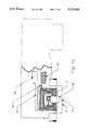
- FIG. 1ais a representational plan view of a prior art thin film head, to aid in the explanation of this invention
- FIG. 1bis a partial lateral cross-sectional view, taken through line A--A of FIG. 1a, of a conventional thin film recording head, depicting planar first and second coils located between the pole pieces;
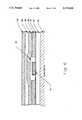
- FIG. 2is a partial cross-sectional view of a thin film head assembly showing an increased coil thickness outside the pole region, in accordance with this invention
- FIG. 3is a partial cross-sectional view showing the first leg of the first coil structure
- FIG. 4is a partial cross-sectional view showing the first and second legs of the first coil structure deposited over the P1 pole piece;
- FIG. 5is a plan view of the first and second legs of the first coil structure relative to the pole pieces of which P1 is shown;
- FIG. 6is a partial cross-sectional view showing the first planar layer or leg of the second coil structure.
- FIG. 7is a partial cross-sectional view of a thin film head assembly incorporating the partly thickened coil structures, in accordance with this invention.
- a typical embodiment of a thin film head assemblycomprises a ceramic substrate 10 preferably made of a material formed from a mixture of aluminum oxide (Al 2 O 3 ) and titanium carbide (TiC).
- the ceramic substrate 10is polished to provide a smooth surface on which a layer of insulating aluminum oxide 12 is deposited by r.f. sputtering, for example.
- the insulating oxide layer 12is lapped and polished to eliminate surface defects.
- an alloy formed from nickel and ironis deposited by r.f. sputtering over the insulating layer 12.
- the pattern of the pole piece P1is formed by means of a mask using standard photolithographic processes.
- a thin film 14 of sputtered aluminum oxideis deposited over the entire surface of the P1 pole piece layer.
- the portion of the oxide film 14 in the area of the back gap of the transduceris removed by standard masking and etching to produce a transducing gap layer.
- the thin oxide film 14 which extends to the tips of pole pieces P1 and P2provides the transducing gap at the transducing surface of the thin film head.
- the P1 pole piece and second pole piece P2which is spaced above P1 and in virtual alignment with P1 provide a magnetic field between the pole pieces.
- the pole piecesare preferably made of a nickel-iron alloy.
- the insulation layer 16serves as a smoothing layer that is fabricated after forming the pole piece P1 and provides a substantially planar surface for the deposition of a first coil structure 18 made of a layer of copper material.
- a second coil structure 22is deposited over an insulating layer 20 that is formed over the first coil structure 18.
- the two coil structures 18 and 22are tied at a connection 17.
- the electrical coils 18 and 22which are fabricated between the pole pieces P1 and P2 conduct current within the magnetic field generated by the pole pieces.
- signalsare directed to the coils 18 and 22 from an external data processing circuit to terminals 23 and 25.
- the data signalsare transduced and converted to magnetic flux signals at the transducing gap 15 formed at the end of gap layer 14 and at the transducing surface of the thin film transducer or head 11.
- Organic insulation layers 16, 20 and 24 made of baked and hardened photoresistare interweaved between the P1 and P2 pole pieces and the coil structures 18 and 22.
- An insulating aluminum oxide overcoat layer 26is r.f. sputtered over the entire thin film head structure to protect against deleterious ambient effects, such as humidity for example.
- the coil structuresare each fabricated with two layers or legs.
- One leg of each coil structureis formed with a conventional thin layer and the second leg is formed to provide a much thicker layer of a portion of the coil structures. The thicker portion is located away from the P1 and P2 pole pieces and outside of the magnetic region between the pole pieces.
- the first leg 28 of the coil structure 38is deposited by well known masking, sputtering, plating and etching processes over the insulating gap layer 14 to form a step segment.
- Insulation layer 16 shown in FIGS. 1b and 2is not depicted in FIGS. 3-7 for the purpose of convenience, as this layer 16 need not be used in some embodiments of the invention.
- the leg 28is spaced from the P1 pole piece so that no portion of the leg 28 is disposed within the region of magnetic flux developed between P1 and P2.
- the upper second layer or leg 32 of the first coil structure 38is deposited over the first leg 28 and additionally over the portion of the insulation 30 formed above the P1 pole piece, as shown in FIG. 4.
- FIG. 5represents the first coil structure 38 with both layers of coils 28 and 32 connected at the interconnect pad 39.
- the thickness of the inner structure of upper second layer 32 of the first coil structure 38, disposed within the magnetic region of the transducer between the pole pieces,is relatively thin, in the range of about 2.5 to 4.0 microns, for example; and the thickness of the lower layer 28 of the first coil 38 outside the magnetic region, where the step segment 28 is provided, is made as thick as possible within manufacturing constraints. At present these manufacturing limitations allow the thickness of the layer 28 to be about the same as the thickness of the layer 32, which results in an overall thickness of the coil 38 of about twice the thickness of the layer 32, or about 5 to 8 microns thick.
- the second leg 32 of the first coil 38is preferably made slightly narrower than the first leg 28 to facilitate coil-to-coil alignment.
- an organic insulation layer 20is deposited over the second leg 32.
- the layer 20provides leveling for facilitating the deposition of the first layer or leg 34 of the second coil structure 40, as shown in FIG. 6.
- the first leg 34is substantially planar and is about the same thickness as the second leg 32 of the first coil 38.
- a second coil leg 36is deposited on the leg 34 by a remask step, similar to the process step used for the first leg 28 of the first coil 38.
- the second leg 36is thickened approximately to the level of the second pole P2.
- the leg 36has a thickness substantially the same as the first leg 28 of the first coil 38.
- the coil structures 38 and 40have configurations which are virtual mirror images of each other.
- An organic insulation layer 24is next formed over the second leg 36 and the P2 pole piece is formed on the baked photoresist layer 24.
- a thick aluminum oxide insulation layer 26is then deposited to serve as an overcoat and protective layer for the thin film magnetic head.
- the coils 38 and 40are electrically connected to complete the signal circuit path.
- the other ends of the coils 38 and 40are connected to pins or terminals which are coupled to external circuitry for passing signals through the head during recording and readout.
- the windings or turns of the coil structure 38are made with a 5 micron pitch comprising 4 micron lines with a 1 micron spacing.
- the distance between the P1 pole piece and the bottom surface of the second leg or layer 32 of coil 38was made to be about 2 to 5 microns.
- the insulation layers 16, 20, and 24are made of organic material, i.e., a cured photoresist, which prevents the coils from electrical shorting to each other as well as to the pole pieces P1 and P2.
- the novel coil assemblyincorporating coil structures having a plurality of coil layers, with one layer formed as a step adjacent to a thin coil layer to thicken the overall coil structure, a desirable reduction in coil resistance of a thin film head is realized.
- the step layeris made as thick as practically possible with present day manufacturing techniques, and is located out of the magnetic region defined by the opposing pole pieces.
- a single coil structure with a thin leg and a thick step legmay be produced to obtain a lowered coil resistance.
- the thicknesses of the coil layermay be varied to accommodate a specific configuration of a thin film head assembly.
- the step segment layermay be much thicker than the thin layer with the portion of the coil structure having the additional thickness outside of the magnetic yoke area thereby effectively decreasing coil resistance.
Landscapes
- Engineering & Computer Science (AREA)
- Manufacturing & Machinery (AREA)
- Magnetic Heads (AREA)
Abstract
Description
Claims (8)
Priority Applications (4)
| Application Number | Priority Date | Filing Date | Title |
|---|---|---|---|
| US07/709,333US5173826A (en) | 1991-06-03 | 1991-06-03 | Thin film head with coils of varying thickness |
| EP19920107969EP0517005A3 (en) | 1991-06-03 | 1992-05-12 | Thin film head with coils of varying thickness |
| JP4138237AJPH05159234A (en) | 1991-06-03 | 1992-05-29 | Thin film head having coil whose thickness is changed |
| US08/407,270US5472736A (en) | 1991-06-03 | 1995-03-20 | Method of making a bi-level coil for a thin film magnetic transducer |
Applications Claiming Priority (1)
| Application Number | Priority Date | Filing Date | Title |
|---|---|---|---|
| US07/709,333US5173826A (en) | 1991-06-03 | 1991-06-03 | Thin film head with coils of varying thickness |
Related Child Applications (1)
| Application Number | Title | Priority Date | Filing Date |
|---|---|---|---|
| US98634192AContinuation-In-Part | 1991-06-03 | 1992-12-07 |
Publications (1)
| Publication Number | Publication Date |
|---|---|
| US5173826Atrue US5173826A (en) | 1992-12-22 |
Family
ID=24849414
Family Applications (1)
| Application Number | Title | Priority Date | Filing Date |
|---|---|---|---|
| US07/709,333Expired - LifetimeUS5173826A (en) | 1991-06-03 | 1991-06-03 | Thin film head with coils of varying thickness |
Country Status (3)
| Country | Link |
|---|---|
| US (1) | US5173826A (en) |
| EP (1) | EP0517005A3 (en) |
| JP (1) | JPH05159234A (en) |
Cited By (22)
| Publication number | Priority date | Publication date | Assignee | Title |
|---|---|---|---|---|
| US5472736A (en)* | 1991-06-03 | 1995-12-05 | Read-Rite Corporation | Method of making a bi-level coil for a thin film magnetic transducer |
| US5764454A (en)* | 1995-12-26 | 1998-06-09 | Read-Rite Smi Corporation | Thin-film magnetic head with improved bonding characteristics and peeling resistance of insulating film to substrate |
| US5831800A (en)* | 1992-05-05 | 1998-11-03 | Magnex Corporation | Miniature transformer for read/write transducer |
| US5875080A (en)* | 1997-09-05 | 1999-02-23 | International Business Machines Corporation | Write head with second coil above pole having coil density less electrically connected first coil below the pole |
| US6178070B1 (en) | 1999-02-11 | 2001-01-23 | Read-Rite Corporation | Magnetic write head and method for making same |
| US6249397B1 (en)* | 1996-06-05 | 2001-06-19 | Fuji Photo Film Co., Ltd. | Device for reading and writing data on magnetic recording layer of photo film |
| US6400526B2 (en) | 1999-05-26 | 2002-06-04 | Read-Rite Corporation | Advanced writer for chip-on-load beam |
| WO2001099112A3 (en)* | 2000-06-20 | 2002-07-11 | Seagate Technology Llc | Disc drive with layered write coil |
| US6493183B1 (en)* | 2000-06-29 | 2002-12-10 | International Business Machines Corporation | Thermally-assisted magnetic recording system with head having resistive heater in write gap |
| US6694603B1 (en)* | 1997-06-24 | 2004-02-24 | Seagate Technology Llc | Process of forming a magnetic microactuator |
| US20040085673A1 (en)* | 2002-10-31 | 2004-05-06 | International Business Machines Corporation | Method and apparatus for an enhanced coplanar conductance structure for inductive heads |
| US20040212922A1 (en)* | 2002-04-04 | 2004-10-28 | Headway Technologies, Inc. | Thin-film magnetic head, method of manufacturing the same, a head gimbal assembly, and a hard disk drive |
| US20050024764A1 (en)* | 2003-07-29 | 2005-02-03 | Hsiao Wen-Chien David | Magnetic head having a write coil structure with a reduced electrical resistance for reducing thermal protrusion |
| US20060034012A1 (en)* | 2003-08-29 | 2006-02-16 | Lam Terence T | Self-aligned coil process in magnetic recording heads |
| US20060126221A1 (en)* | 2004-12-10 | 2006-06-15 | Kiyoshi Kobayashi | Magnetic head having toroidal coil layer and manufacturing method thereof |
| US20060288564A1 (en)* | 2003-09-29 | 2006-12-28 | Headway Technologies Inc | Thin-film magnetic head, a head gimbal assembly, and a hard disk drive |
| US7457079B2 (en)* | 2002-07-03 | 2008-11-25 | Sony Corporation | Magnetic head with rectangular-shaped planar spiral coil and leading core width smaller than trailing core width |
| US8786983B1 (en) | 2012-06-25 | 2014-07-22 | Western Digital (Fremont), Llc | Magnetic writer having a low aspect ratio two layer coil |
| US8797684B1 (en) | 2011-12-20 | 2014-08-05 | Western Digital (Fremont), Llc | Magnetic writer configured for high data rate recording |
| US8842388B2 (en) | 2008-02-26 | 2014-09-23 | HGST Netherlands BV | Perpendicular magnetic recording head and method for manufacturing the same |
| US9196275B1 (en) | 2014-03-12 | 2015-11-24 | Western Digital Technologies, Inc. | Magnetic head separator fin material to prevent particulate contamination on slider |
| US9245545B1 (en) | 2013-04-12 | 2016-01-26 | Wester Digital (Fremont), Llc | Short yoke length coils for magnetic heads in disk drives |
Families Citing this family (1)
| Publication number | Priority date | Publication date | Assignee | Title |
|---|---|---|---|---|
| JP2005285236A (en)* | 2004-03-30 | 2005-10-13 | Fujitsu Ltd | Magnetic head structure |
Citations (11)
| Publication number | Priority date | Publication date | Assignee | Title |
|---|---|---|---|---|
| US3987488A (en)* | 1974-06-05 | 1976-10-19 | Matsushita Electric Industrial Co., Ltd. | Multi-tracks magnetic head with single turn winding structure |
| US4219854A (en)* | 1978-12-21 | 1980-08-26 | International Business Machines Corporation | Thin film magnetic head assembly |
| US4295173A (en)* | 1979-10-18 | 1981-10-13 | International Business Machines Corporation | Thin film inductive transducer |
| US4375657A (en)* | 1980-11-03 | 1983-03-01 | Brock George W | Magnetic head assembly |
| US4639289A (en)* | 1984-02-03 | 1987-01-27 | Commissariat A L'energie Atomique | Process for producing a magnetic read - write head and head obtained by this process |
| US4685014A (en)* | 1981-08-14 | 1987-08-04 | Computer Basic Technology Association | Production method of thin film magnetic head |
| US4751599A (en)* | 1984-08-06 | 1988-06-14 | Fuji Photo Film Co., Ltd. | Thin-film magnetic head with a coil conductor having a plurality of turns of different widths |
| US4752850A (en)* | 1984-06-06 | 1988-06-21 | Hitachi, Ltd. | Multi-track magnetic thin film heads |
| US4760481A (en)* | 1986-07-11 | 1988-07-26 | Hitachi, Ltd. | Thin film magnetic head having an improved coil |
| US4771350A (en)* | 1984-12-28 | 1988-09-13 | Bull S.A. (Societe Anonyme) | Magnetic reading/writing transducer for perpendicular recording |
| US4860140A (en)* | 1985-09-25 | 1989-08-22 | Hitachi, Ltd. | Magnetic head closure having ferrite substrate and closure and conductive thin film coil deposited in recess of substantially same shape in ferrite substrate |
Family Cites Families (2)
| Publication number | Priority date | Publication date | Assignee | Title |
|---|---|---|---|---|
| US4713711A (en)* | 1985-05-08 | 1987-12-15 | International Business Machines | Thin film magnetic transducer having center tapped winding |
| NL9001147A (en)* | 1990-05-17 | 1991-12-16 | Philips Nv | THIN MOVIE MAGNETIC HEAD. |
- 1991
- 1991-06-03USUS07/709,333patent/US5173826A/ennot_activeExpired - Lifetime
- 1992
- 1992-05-12EPEP19920107969patent/EP0517005A3/ennot_activeWithdrawn
- 1992-05-29JPJP4138237Apatent/JPH05159234A/enactivePending
Patent Citations (11)
| Publication number | Priority date | Publication date | Assignee | Title |
|---|---|---|---|---|
| US3987488A (en)* | 1974-06-05 | 1976-10-19 | Matsushita Electric Industrial Co., Ltd. | Multi-tracks magnetic head with single turn winding structure |
| US4219854A (en)* | 1978-12-21 | 1980-08-26 | International Business Machines Corporation | Thin film magnetic head assembly |
| US4295173A (en)* | 1979-10-18 | 1981-10-13 | International Business Machines Corporation | Thin film inductive transducer |
| US4375657A (en)* | 1980-11-03 | 1983-03-01 | Brock George W | Magnetic head assembly |
| US4685014A (en)* | 1981-08-14 | 1987-08-04 | Computer Basic Technology Association | Production method of thin film magnetic head |
| US4639289A (en)* | 1984-02-03 | 1987-01-27 | Commissariat A L'energie Atomique | Process for producing a magnetic read - write head and head obtained by this process |
| US4752850A (en)* | 1984-06-06 | 1988-06-21 | Hitachi, Ltd. | Multi-track magnetic thin film heads |
| US4751599A (en)* | 1984-08-06 | 1988-06-14 | Fuji Photo Film Co., Ltd. | Thin-film magnetic head with a coil conductor having a plurality of turns of different widths |
| US4771350A (en)* | 1984-12-28 | 1988-09-13 | Bull S.A. (Societe Anonyme) | Magnetic reading/writing transducer for perpendicular recording |
| US4860140A (en)* | 1985-09-25 | 1989-08-22 | Hitachi, Ltd. | Magnetic head closure having ferrite substrate and closure and conductive thin film coil deposited in recess of substantially same shape in ferrite substrate |
| US4760481A (en)* | 1986-07-11 | 1988-07-26 | Hitachi, Ltd. | Thin film magnetic head having an improved coil |
Cited By (33)
| Publication number | Priority date | Publication date | Assignee | Title |
|---|---|---|---|---|
| US5472736A (en)* | 1991-06-03 | 1995-12-05 | Read-Rite Corporation | Method of making a bi-level coil for a thin film magnetic transducer |
| US5831800A (en)* | 1992-05-05 | 1998-11-03 | Magnex Corporation | Miniature transformer for read/write transducer |
| US5764454A (en)* | 1995-12-26 | 1998-06-09 | Read-Rite Smi Corporation | Thin-film magnetic head with improved bonding characteristics and peeling resistance of insulating film to substrate |
| US6249397B1 (en)* | 1996-06-05 | 2001-06-19 | Fuji Photo Film Co., Ltd. | Device for reading and writing data on magnetic recording layer of photo film |
| US6694603B1 (en)* | 1997-06-24 | 2004-02-24 | Seagate Technology Llc | Process of forming a magnetic microactuator |
| US5875080A (en)* | 1997-09-05 | 1999-02-23 | International Business Machines Corporation | Write head with second coil above pole having coil density less electrically connected first coil below the pole |
| US6178070B1 (en) | 1999-02-11 | 2001-01-23 | Read-Rite Corporation | Magnetic write head and method for making same |
| US6400526B2 (en) | 1999-05-26 | 2002-06-04 | Read-Rite Corporation | Advanced writer for chip-on-load beam |
| GB2379793B (en)* | 2000-06-20 | 2004-03-17 | Seagate Technology Llc | Disc drive with layered write coil |
| GB2379793A (en)* | 2000-06-20 | 2003-03-19 | Seagate Technology Llc | Disc drive with layered write coil |
| US6654202B2 (en) | 2000-06-20 | 2003-11-25 | Seagate Technology Llc | Disc drive with layered write coil |
| WO2001099112A3 (en)* | 2000-06-20 | 2002-07-11 | Seagate Technology Llc | Disc drive with layered write coil |
| US6493183B1 (en)* | 2000-06-29 | 2002-12-10 | International Business Machines Corporation | Thermally-assisted magnetic recording system with head having resistive heater in write gap |
| US20040212922A1 (en)* | 2002-04-04 | 2004-10-28 | Headway Technologies, Inc. | Thin-film magnetic head, method of manufacturing the same, a head gimbal assembly, and a hard disk drive |
| US7119987B2 (en)* | 2002-04-04 | 2006-10-10 | Headway Technologies Inc. | Thin-film magnetic head, a head gimbal assembly, and a hard disk drive |
| US7457079B2 (en)* | 2002-07-03 | 2008-11-25 | Sony Corporation | Magnetic head with rectangular-shaped planar spiral coil and leading core width smaller than trailing core width |
| US6980395B2 (en)* | 2002-10-31 | 2005-12-27 | International Business Machines Corporation | Enhanced coplanar conductance structure for inductive heads |
| US20040085673A1 (en)* | 2002-10-31 | 2004-05-06 | International Business Machines Corporation | Method and apparatus for an enhanced coplanar conductance structure for inductive heads |
| US7509730B2 (en) | 2002-10-31 | 2009-03-31 | International Business Machines Corporation | Method and apparatus for an enhanced coplanar conductance structure for inductive heads |
| US20050024764A1 (en)* | 2003-07-29 | 2005-02-03 | Hsiao Wen-Chien David | Magnetic head having a write coil structure with a reduced electrical resistance for reducing thermal protrusion |
| US7079353B2 (en)* | 2003-07-29 | 2006-07-18 | Hitachi Global Storage Technologies Netherlands B.V. | Magnetic head having a write coil structure with a reduced electrical resistance for reducing thermal protrusion |
| US7190552B2 (en) | 2003-07-29 | 2007-03-13 | Hitachi Global Storage Technologies Netherlands B.V. | Magnetic head having a damascene-fabricated write coil structure with coil layers extending between the poles for reduced electrical resistance |
| US20060152849A1 (en)* | 2003-07-29 | 2006-07-13 | Hsiao Wen-Chien D | Magnetic head having a write coil structure with a reduced electrical resistance for reducing thermal protrusion |
| US20060034012A1 (en)* | 2003-08-29 | 2006-02-16 | Lam Terence T | Self-aligned coil process in magnetic recording heads |
| US20060288564A1 (en)* | 2003-09-29 | 2006-12-28 | Headway Technologies Inc | Thin-film magnetic head, a head gimbal assembly, and a hard disk drive |
| US7168156B2 (en) | 2003-09-29 | 2007-01-30 | Headway Technologies, Inc. | Method of manufacturing a thin-film magnetic head |
| US20060126221A1 (en)* | 2004-12-10 | 2006-06-15 | Kiyoshi Kobayashi | Magnetic head having toroidal coil layer and manufacturing method thereof |
| US7667927B2 (en)* | 2004-12-10 | 2010-02-23 | Tdk Corporation | Magnetic head having toroidal coil layer and manufacturing method thereof |
| US8842388B2 (en) | 2008-02-26 | 2014-09-23 | HGST Netherlands BV | Perpendicular magnetic recording head and method for manufacturing the same |
| US8797684B1 (en) | 2011-12-20 | 2014-08-05 | Western Digital (Fremont), Llc | Magnetic writer configured for high data rate recording |
| US8786983B1 (en) | 2012-06-25 | 2014-07-22 | Western Digital (Fremont), Llc | Magnetic writer having a low aspect ratio two layer coil |
| US9245545B1 (en) | 2013-04-12 | 2016-01-26 | Wester Digital (Fremont), Llc | Short yoke length coils for magnetic heads in disk drives |
| US9196275B1 (en) | 2014-03-12 | 2015-11-24 | Western Digital Technologies, Inc. | Magnetic head separator fin material to prevent particulate contamination on slider |
Also Published As
| Publication number | Publication date |
|---|---|
| EP0517005A2 (en) | 1992-12-09 |
| JPH05159234A (en) | 1993-06-25 |
| EP0517005A3 (en) | 1993-12-15 |
Similar Documents
| Publication | Publication Date | Title |
|---|---|---|
| US5173826A (en) | Thin film head with coils of varying thickness | |
| US6195232B1 (en) | Low-noise toroidal thin film head with solenoidal coil | |
| US5995342A (en) | Thin film heads having solenoid coils | |
| US7522379B1 (en) | Write element with recessed pole and heat sink layer for ultra-high density writing | |
| US7238292B1 (en) | Method of fabricating a write element with a reduced yoke length | |
| US4295173A (en) | Thin film inductive transducer | |
| US6496330B1 (en) | Magnetic write head having a splitcoil structure | |
| JPS6010410A (en) | Thin film magnetic converter | |
| JP2768372B2 (en) | Composite type thin film magnetic head | |
| JPH07296331A (en) | Magnetic head assembly having write pole structure having shield | |
| JP3345588B2 (en) | Thin film magnetic head and method of manufacturing the same | |
| EP0514600B1 (en) | Thin film transducer/transformer assembly | |
| JP3149851B2 (en) | Thin film magnetic head | |
| US5969911A (en) | Inductive/MR composite type thin-film magnetic head | |
| US5472736A (en) | Method of making a bi-level coil for a thin film magnetic transducer | |
| JPS59195311A (en) | Vertical magnetic head | |
| US5694276A (en) | Shielded magnetic head having an inductive coil with low mutual inductance | |
| JP4006164B2 (en) | Recording / reproducing type thin film head and method of manufacturing the head | |
| KR100224648B1 (en) | Thin film head with coils of varying thickness | |
| JP2722948B2 (en) | Thin film magnetic head | |
| JPH04356707A (en) | Thin film magnetic head | |
| JP2551749B2 (en) | Method of manufacturing thin film magnetic head | |
| JP2635670B2 (en) | Thin film magnetic head | |
| JPS5856223A (en) | thin film magnetic head | |
| JPH05242426A (en) | Thin-film magnetic head and its producing method |
Legal Events
| Date | Code | Title | Description |
|---|---|---|---|
| AS | Assignment | Owner name:READ-RITE CORPORATION A CORP. OF CALIFORNIA, CAL Free format text:ASSIGNMENT OF ASSIGNORS INTEREST.;ASSIGNOR:BISCHOFF, PETER G.;REEL/FRAME:005734/0115 Effective date:19910528 | |
| STCF | Information on status: patent grant | Free format text:PATENTED CASE | |
| FPAY | Fee payment | Year of fee payment:4 | |
| AS | Assignment | Owner name:CANADIAN IMPERIAL BANK OF COMMERCE, NEW YORK Free format text:SECURITY AGREEMENT;ASSIGNOR:READ-RITE CORPORATION, A DELAWARE CORPORATION;REEL/FRAME:009500/0342 Effective date:19980814 | |
| FPAY | Fee payment | Year of fee payment:8 | |
| AS | Assignment | Owner name:READ-RITE CORPORATION, CALIFORNIA Free format text:ASSIGNMENT AND RELEASE OF INTELLECTUAL PROPERTY SECURITY;ASSIGNOR:CANADIAN IMPERIAL BANK OF COMMERCE NEW YORK AGENCY, AS AGENT;REEL/FRAME:011675/0822 Effective date:20010326 | |
| AS | Assignment | Owner name:TENNENBAUM CAPITAL PARTNERS, LLC, CALIFORNIA Free format text:SECURITY INTEREST;ASSIGNOR:READ-RITE CORPORATION;REEL/FRAME:013616/0399 Effective date:20021224 | |
| AS | Assignment | Owner name:WESTERN DIGITAL (FREMONT), INC., CALIFORNIA Free format text:ASSIGNMENT OF ASSIGNORS INTEREST;ASSIGNOR:READ-RITE CORPORATION;REEL/FRAME:014506/0765 Effective date:20030731 | |
| AS | Assignment | Owner name:READ-RITE CORPORATION, CALIFORNIA Free format text:RELEASE OF SECURITY INTEREST;ASSIGNOR:TENNENBAUM CAPITAL PARTNERS, LLC;REEL/FRAME:014499/0476 Effective date:20030731 | |
| FPAY | Fee payment | Year of fee payment:12 | |
| AS | Assignment | Owner name:GENERAL ELECTRIC CAPITAL CORPORATION, AS AGENT, CA Free format text:SECURITY INTEREST;ASSIGNORS:WESTERN DIGITAL TECHNOLOGIES, INC.;WESTERN DIGITAL (FREMONT), INC.;REEL/FRAME:014830/0957 Effective date:20030919 | |
| AS | Assignment | Owner name:WESTERN DIGITAL TECHNOLOGIES, INC., CALIFORNIA Free format text:RELEASE BY SECURED PARTY;ASSIGNOR:GENERAL ELECTRIC CAPITAL CORPORATION, AS AGENT;REEL/FRAME:020599/0489 Effective date:20070809 Owner name:WESTERN DIGITAL (FREMONT), INC., CALIFORNIA Free format text:RELEASE BY SECURED PARTY;ASSIGNOR:GENERAL ELECTRIC CAPITAL CORPORATION, AS AGENT;REEL/FRAME:020599/0489 Effective date:20070809 | |
| AS | Assignment | Owner name:WESTERN DIGITAL TECHNOLOGIES, INC., CALIFORNIA Free format text:ASSIGNMENT OF ASSIGNORS INTEREST;ASSIGNOR:WESTERN DIGITAL (FREMONT), LLC;REEL/FRAME:050450/0582 Effective date:20190508 |