US5172338A - Multi-state EEprom read and write circuits and techniques - Google Patents
Multi-state EEprom read and write circuits and techniquesDownload PDFInfo
- Publication number
- US5172338A US5172338AUS07/508,273US50827390AUS5172338AUS 5172338 AUS5172338 AUS 5172338AUS 50827390 AUS50827390 AUS 50827390AUS 5172338 AUS5172338 AUS 5172338A
- Authority
- US
- United States
- Prior art keywords
- cells
- memory
- addressed
- cell
- eeprom
- Prior art date
- Legal status (The legal status is an assumption and is not a legal conclusion. Google has not performed a legal analysis and makes no representation as to the accuracy of the status listed.)
- Expired - Lifetime
Links
Images


Classifications
- G—PHYSICS
- G11—INFORMATION STORAGE
- G11C—STATIC STORES
- G11C11/00—Digital stores characterised by the use of particular electric or magnetic storage elements; Storage elements therefor
- G11C11/56—Digital stores characterised by the use of particular electric or magnetic storage elements; Storage elements therefor using storage elements with more than two stable states represented by steps, e.g. of voltage, current, phase, frequency
- G11C11/5621—Digital stores characterised by the use of particular electric or magnetic storage elements; Storage elements therefor using storage elements with more than two stable states represented by steps, e.g. of voltage, current, phase, frequency using charge storage in a floating gate
- G11C11/5628—Programming or writing circuits; Data input circuits
- G11C11/5635—Erasing circuits
- G—PHYSICS
- G11—INFORMATION STORAGE
- G11C—STATIC STORES
- G11C11/00—Digital stores characterised by the use of particular electric or magnetic storage elements; Storage elements therefor
- G11C11/56—Digital stores characterised by the use of particular electric or magnetic storage elements; Storage elements therefor using storage elements with more than two stable states represented by steps, e.g. of voltage, current, phase, frequency
- G11C11/5621—Digital stores characterised by the use of particular electric or magnetic storage elements; Storage elements therefor using storage elements with more than two stable states represented by steps, e.g. of voltage, current, phase, frequency using charge storage in a floating gate
- G11C11/5642—Sensing or reading circuits; Data output circuits
- G—PHYSICS
- G11—INFORMATION STORAGE
- G11C—STATIC STORES
- G11C16/00—Erasable programmable read-only memories
- G11C16/02—Erasable programmable read-only memories electrically programmable
- G11C16/06—Auxiliary circuits, e.g. for writing into memory
- G11C16/10—Programming or data input circuits
- G—PHYSICS
- G11—INFORMATION STORAGE
- G11C—STATIC STORES
- G11C16/00—Erasable programmable read-only memories
- G11C16/02—Erasable programmable read-only memories electrically programmable
- G11C16/06—Auxiliary circuits, e.g. for writing into memory
- G11C16/10—Programming or data input circuits
- G11C16/14—Circuits for erasing electrically, e.g. erase voltage switching circuits
- G11C16/16—Circuits for erasing electrically, e.g. erase voltage switching circuits for erasing blocks, e.g. arrays, words, groups
- G—PHYSICS
- G11—INFORMATION STORAGE
- G11C—STATIC STORES
- G11C16/00—Erasable programmable read-only memories
- G11C16/02—Erasable programmable read-only memories electrically programmable
- G11C16/06—Auxiliary circuits, e.g. for writing into memory
- G11C16/26—Sensing or reading circuits; Data output circuits
- G11C16/28—Sensing or reading circuits; Data output circuits using differential sensing or reference cells, e.g. dummy cells
- G—PHYSICS
- G11—INFORMATION STORAGE
- G11C—STATIC STORES
- G11C16/00—Erasable programmable read-only memories
- G11C16/02—Erasable programmable read-only memories electrically programmable
- G11C16/06—Auxiliary circuits, e.g. for writing into memory
- G11C16/34—Determination of programming status, e.g. threshold voltage, overprogramming or underprogramming, retention
- G11C16/3436—Arrangements for verifying correct programming or erasure
- G11C16/344—Arrangements for verifying correct erasure or for detecting overerased cells
- G11C16/3445—Circuits or methods to verify correct erasure of nonvolatile memory cells
- G—PHYSICS
- G11—INFORMATION STORAGE
- G11C—STATIC STORES
- G11C16/00—Erasable programmable read-only memories
- G11C16/02—Erasable programmable read-only memories electrically programmable
- G11C16/06—Auxiliary circuits, e.g. for writing into memory
- G11C16/34—Determination of programming status, e.g. threshold voltage, overprogramming or underprogramming, retention
- G11C16/3436—Arrangements for verifying correct programming or erasure
- G11C16/3454—Arrangements for verifying correct programming or for detecting overprogrammed cells
- G11C16/3459—Circuits or methods to verify correct programming of nonvolatile memory cells
- G—PHYSICS
- G11—INFORMATION STORAGE
- G11C—STATIC STORES
- G11C7/00—Arrangements for writing information into, or reading information out from, a digital store
- G11C7/04—Arrangements for writing information into, or reading information out from, a digital store with means for avoiding disturbances due to temperature effects
- G—PHYSICS
- G11—INFORMATION STORAGE
- G11C—STATIC STORES
- G11C2211/00—Indexing scheme relating to digital stores characterized by the use of particular electric or magnetic storage elements; Storage elements therefor
- G11C2211/56—Indexing scheme relating to G11C11/56 and sub-groups for features not covered by these groups
- G11C2211/562—Multilevel memory programming aspects
- G11C2211/5621—Multilevel programming verification
- G—PHYSICS
- G11—INFORMATION STORAGE
- G11C—STATIC STORES
- G11C2211/00—Indexing scheme relating to digital stores characterized by the use of particular electric or magnetic storage elements; Storage elements therefor
- G11C2211/56—Indexing scheme relating to G11C11/56 and sub-groups for features not covered by these groups
- G11C2211/563—Multilevel memory reading aspects
- G11C2211/5631—Concurrent multilevel reading of more than one cell
- G—PHYSICS
- G11—INFORMATION STORAGE
- G11C—STATIC STORES
- G11C2211/00—Indexing scheme relating to digital stores characterized by the use of particular electric or magnetic storage elements; Storage elements therefor
- G11C2211/56—Indexing scheme relating to G11C11/56 and sub-groups for features not covered by these groups
- G11C2211/563—Multilevel memory reading aspects
- G11C2211/5634—Reference cells
- G—PHYSICS
- G11—INFORMATION STORAGE
- G11C—STATIC STORES
- G11C2211/00—Indexing scheme relating to digital stores characterized by the use of particular electric or magnetic storage elements; Storage elements therefor
- G11C2211/56—Indexing scheme relating to G11C11/56 and sub-groups for features not covered by these groups
- G11C2211/564—Miscellaneous aspects
- G11C2211/5645—Multilevel memory with current-mirror arrangements
Definitions
- This inventionrelates generally to semiconductor electrically erasable programmable read only memories (EEprom), and specifically to circuits and techniques for reading and programming their state.
- Epromsemiconductor electrically erasable programmable read only memories
- EEprom and electrically programmable read only memoryare typically used in digital circuits for non-volatile storage of data or program. They can be erased and have new data written or "programmed” into their memory cells.
- An Epromutilizes a floating (unconnected) conductive gate, in a field effect transistor structure, positioned over but insulated from a channel region in a semiconductor substrate, between source and drain regions.
- a control gateis then provided over the floating gate, but also insulated therefrom.
- the threshold voltage characteristic of the transistoris controlled by the amount of charge that is retained on the floating gate. That is, the minimum amount of voltage (threshold) that must be applied to the control gate before the transistor is turned “on” to permit conduction between its source and drain regions is controlled by the level of charge on the floating gate.
- the floating gatecan hold a range of charge and therefore an Eprom memory cell can be programmed to any threshold level within a threshold window.
- the size of the threshold windowdelimited by the minimum and maximum threshold levels of the device, depends on the device's characteristics, operating conditions and history. Each distinct threshold level within the window may, in principle, be used to designate a definite memory state of the cell.
- the transistor serving as a memory cellis programmed to one of two states by accelerating electrons from the substrate channel region, through a thin gate dielectric and onto the floating gate.
- the memory statesare erasable by removing the charge on the floating gate by ultra-violet radiation.
- An electrically erasable and programmable read only memoryhas a similar structure but additionally provides a mechanism for removing charge from its floating gate upon application of proper voltages.
- An array of such EEprom cellsis referred to as a "Flash" EEprom array when an entire array of cells, or significant group of cells of the array, is erased simultaneously (i.e., in a flash). Once erased, a cell can then be reprogrammed.
- a specific, single cell in a two-dimensional array of Eprom, EEprom cellsis addressed for reading by application of a source-drain voltage to source and drain lines in a column containing the cell being addressed, and application of a control gate voltage to a word line connected to the control gates in a row containing the cell being addressed.
- An addressed memory cell transistor's stateis read by placing an operating voltage across its source and drain and on its control gate, and then detecting the level of current flowing between the source and drain.
- the level of currentis proportional to the threshold level of the transistor, which in turn is determined by the amount of charge on its floating gate.
- one breakpoint threshold levelis established so as to partition the threshold window into two regions.
- the source/drain currentis compared with the breakpoint threshold level that was used when the cell was programmed. If the current read is higher than that of the threshold, the cell is determined to be in a "zero" state, while if the current is less than that of the threshold, the cell is determined to be in the other state.
- a current sourcewhich may be externally programmable is often provided as part of a memory system to generate the breakpoint threshold current.
- each cellstores two or more bits of data.
- the information that a given EEprom array can storeis thus increased by the multiple of number of states that each cell can store.
- Flash EEprom structurecapable of an increased lifetime as measured by the number of program/read cycles that the memory can endure.
- the multiple threshold breakpoint levelsare provided by a set of memory cells which serves as master reference cells.
- the master reference cellsare independently and externally programmable, either by the memory manufacturer or the user. This feature provides maximum flexibility, allowing the breakpoint thresholds to be individually set within the threshold window of the device at any time. Also, by virtue of being an identical device as that of the memory cells, the reference cells closely track the same variations due to manufacturing processes, operating conditions and device aging.
- the independent programmability of each breakpoint threshold levelallows optimization and fine-tuning of the threshold window's partitioning, critical in multi-state implementation. Furthermore, it allows post-manufacture configuration for either 2-state or multi-state memory from the same device, depending on user need or device characteristics at the time.
- a set of memory cells within each sectorare set aside as local reference cells.
- Each set of reference cellstracks the Flash cells in the same sector closely as they are both cycled through the same number of program/erase cycles. Thus, the aging that occurs in the memory cells of a sector after a large number of erase/reprogram cycles is also reflected in the local reference cells.
- the set of individual breakpoint threshold levelsare re-programmed to the associated local reference cells. The threshold levels read from the local reference cells then automatically adjust to changing conditions of the memory cells of the same sector. The threshold window's partitioning is thus optimally maintained. This technique is also useful for a memory that employs only a single reference cell that is used to read two state (1 bit) memory cells.
- the threshold levels rewritten at each cycle to the local reference cellsare obtained from a set of master cells which are not cycled along with the memory cells but rather which retain a charge that has been externally programmed (or reprogrammed). Only a single set of master memory cells is needed for an entire memory integrated circuit.
- the read operationdirectly uses the threshold levels in the local reference cells previously copied from the master reference cells.
- the read operationindirectly uses the threshold levels in the local reference cells even though the reading is done relative to the master reference cells. It does this by first reading the local reference cells relative to the master reference cells. The differences detected are used to offset subsequent regular readings of memory cells relative to the master reference cells so that the biased readings are effectively relative to the local reference cells.
- a read operation on a memory celldetermines which memory state it is in by comparing the current flowing therethrough with that of a set of reference currents corresponding to the multiple threshold breakpoint levels.
- the current flowing through a cell being readis compared one-by-one with each of the threshold current levels of the reference cells.
- the current flowing through a cell to be readis compared simultaneously with that of the set of reference cells.
- a special current mirror configurationreproduces the current to be read without degrading its signal, into multiple branches, one for each threshold current comparison.
- a circuitverifies the programmed state after each programming step with the intended state and selectively inhibits further programming of any cells in the chunk that have been verified to have been programmed correctly. This enables efficient parallel programming of a chunk of data in a multi-state implementation.
- an erased stateis obtained by repetitive steps of erasing and verifying from the existing state to the "erased" state, a circuit verifies the erased state after each erasing step with the "erased” state and selectively inhibits further erasing of any cells in the chunk that have been verified to have been erased correctly. This prevents over-erasing which is stressful to the device and enables efficient parallel erasing of a group of cells.
- the cellsare re-programmed to the state adjacent the "erased” state. This ensures that each erased cell starts from a well defined state, and also allows each cell to undergo similar program/erase stress.
- FIG. 1is a cross-sectional view of an EEprom device integrated circuit structure that can be used to implement the various aspects of the present invention
- FIG. 2is a view of the structure of FIG. 1 taken across section 2--2 thereof;
- FIG. 3is an equivalent circuit of a single EEprom cell of the type illustrated in FIGS. 1 and 2;
- FIG. 4shows an addressable array of EEprom cells
- FIG. 5is a block diagram of an EEprom system in which the various aspects of the present invention are implemented
- FIG. 6illustrates the partitioning of the threshold window of an EEprom cell which stores one bit of data
- FIG. 7Aillustrates the partitioning of the threshold window of an EEprom cell which stores two bits of data
- FIG. 7Billustrates the partitioning of the source-drain conduction current threshold window of the EEprom cell of FIG. 7A;
- FIGS. 8A and 8Bare curves that illustrate the changes and characteristics of a typical EEprom after a period of use
- FIG. 9Aillustrates read and program circuits for a master reference cell and an addressed memory cell according to the present invention
- FIG. 9Billustrates multi-state read circuits with reference cells according to the present invention.
- FIGS. 9C(1)-9C(8)illustrate the timing for multi-state read for the circuits of FIG. 9B;
- FIG. 9Dillustrates one embodiment of a multi-state read circuit in which the memory state of an address cell is sensed relative to a set of reference current levels simultaneously;
- FIG. 9Eillustrates one embodiment of an IREF circuit shown in FIG. 9D as an EEprom cell programmed with a reference current
- FIG. 9Fillustrates a preferred implementation of the embodiment in FIG. 9D in which each IREF circuit is provided by a current source reproducing a reference current programmed in the EEprom cell;
- FIG. 9Gillustrates another embodiment of an IREF circuit shown in FIG. 9D in which a reference current is provided in each branch by the conduction of a transistor of predetermined size;
- FIG. 9Hillustrates another embodiment of a multi-state read circuit in which the memory state of an address cell is sensed relative to a set of reference current levels simultaneously;
- FIG. 9Iillustrates yet another embodiment of a multi-state read circuit in which the memory state of an address cell is sensed relative to a set of reference current levels simultaneously;
- FIG. 10illustrates a specific memory organization according to the present invention
- FIG. 11shows an algorithm for programming a set of local reference cells according to the present invention
- FIG. 12Ashows one embodiment of a read circuit using local reference cells directly
- FIG. 12Bshows a read algorithm for the embodiment of FIG. 12A
- FIG. 13Ashows an alternative embodiment of a read circuit using local reference cells indirectly
- FIG. 13Bis a programmable circuit for the biased reading of the master reference cells according the alternative embodiment
- FIG. 13Cis a detail circuit diagram for the programmable biasing circuit of FIG. 13B;
- FIG. 13Dshows a read algorithm for the embodiment of FIG. 13A
- FIG. 14illustrates the read/program data paths for a chunk of cell in parallel
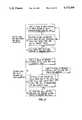
- FIG. 15shows an on chip program/verify algorithm according to the present invention
- FIG. 16is a circuit diagram for the compare circuit according to the present invention.
- FIG. 17is a circuit diagram for the program circuit with inhibit according to the present invention.
- FIGS. 18 and 19show Tables 1 and 2 which list typical examples of operating voltages for the EEprom cell of the present invention.
- Eprom, EEprom semiconductor integrated circuit structuresthat can be utilized in making a memory array with which the various aspects of the present invention are advantageously implemented.
- a preferred EEprom structureis generally illustrated in the integrated circuit cross-sectional views of FIGS. 1 and 2. Describing this preferred structure briefly, two memory cells 11 and 13 are formed on a lightly p-doped substrate 15. A heavily n-doped implanted region 17 between the cells 11 and 13 serves as a drain for the cell 11 and a source for the cell 13. Similarly, another implanted n-doped region 19 is the source of the cell 11 and the drain of an adjacent cell, and similarly for another n-doped region 21.
- Each of the memory cells 11 and 13contains respective conductive floating gates 23 and 25, generally made of polysilicon material. Each of these floating gates is surrounded by dielectric material so as to be insulated from each other and any other conductive elements of the structure.
- a control gate 27extends across both of the cells 11 and 13 in a manner to be insulated from the floating gates and the substrate itself.
- conductive strips 29 and 31are additionally provided to be insulated from each other and other conductive elements of the structure, serving as erase gates.
- a pair of such erase gatessurrounds the floating gate of each memory cell and are separated from it by an erase dielectric layer.
- the cellsare isolated by thick field oxide regions, such as regions 33, 35, and 37, shown in the cross-section of FIG. 1, and regions 39 and 41 shown in the view of FIG. 2.
- the memory cellis programmed by transferring electrons from the substrate 15 to a floating gate, such as the floating gate 25 of the memory cell 13.
- the charge on the floating gate 25is increased by electrons travelling across the dielectric from a heavily p-doped region 43 and onto the floating gate. Charge is removed from the floating gate through the dielectric between it and the erase gates 29 and 31.
- the EEprom structure illustrated in FIGS. 1 and 2is a "split-channel" type. Each cell may be viewed as a composite transistor consisting of two transistor T1 and T2 in series as shown in FIG. 3.
- the T1 transistor 11ais formed along the length L1 of the channel of the cell 11 of FIG. 1. It has a variable threshold voltage V T1 .
- the T2 transistor 11bIn series with the T1 transistor 11a is the T2 transistor 11b that is formed in a portion of the channel L2. It has a fixed threshold voltage V T2 of about 1 V.
- Elements of the equivalent circuit of FIG. 3are labeled with the same reference numbers as used for corresponding parts in FIGS. 1 and 2, with a prime (') added.
- the level of charge on the T1's floating gate 23' of an EEprom cellaffects the threshold voltage V T1 of the T1 transistor 11a when operated with the control gate 27'.
- a number of memory statesmay be defined in a cell, corresponding to well defined threshold voltages programmed into the cell by appropriate amount of charges placed on the floating gate. The programming is performed by applying, over a certain period of time, appropriate voltages to the cell's control gate 27' as well as drain 17' and source 19'.
- FIG. 4illustrates schematically an array of individually addressable EEprom cells 60. Each cell is equivalent to the one shown in FIG. 3, having a control gate, source and drain, and an erase gate.
- the plurality of individual memory cellsare organized in rows and columns. Each cell is addressed by selectively energizing its row and column simultaneously.
- a column 62for example, includes a first memory cell 63, an adjacent second memory cell 65, and so forth.
- a second column 72includes memory cells 73, 75, and so forth. Cells 63 and 73 are located in a row 76, cells 65 and 71 in another, adjacent row, and so forth.
- a word lineis connected to all the control gates of the cells in the row.
- the row 76has the word line 77 and the next row has the word line 79.
- a row decoder 81selectively connects the control gate voltage V CG on an input line 83 to all the control gates along a selected word line for a row.
- a column decoder 101selectively connects the source voltage V S on an input line 103 to all the sources and connects the drain voltage V D on an input line 105 to all the drains along a selected column.
- Each cellis addressed by the row and column in which it is located. For example, if the cell 75 is addressed for programming or reading, appropriate programming or reading voltages must be supplied to the cell's control gate, source and drain.
- An address on the internal address bus 111is used to decode row decoder 81 for connecting V CG to the word line 79 connected to the control gate of the cell 75. The same address is used to decode column decoder 101 for connecting V S to the source line 93 and V D to the drain line 95, which are respectively connected to the source and drain of the cell 75.
- One aspect of the present inventionis the implementation of programming and reading of a plurality of memory cells in parallel.
- the column decodercontrols the switching of a source multiplexer 107 and a drain multiplexer 109.
- the selected plurality of columnsmay have their source lines and drain lines made accessible for connection to V S and V D respectively.
- Access to the erase gate of each cellis similar to that of the control gate.
- an erase linesuch as 113 or 115 or 117 is connected to the erase gate of each cells in a row.
- An erase decoder 119decodes an address on the internal address bus 111 and selectively connects the erase voltage V EG on input line 121 to an erase line. This allows each row of cells to be addressed independently, such as the row 76 being simultaneously (Flash) erased by proper voltages applied to their erase gates through erase line 113. In this case, the Flash cell consists of one row of memory cells. However, other Flash cell's implementations are possible and most applications will provide for simultaneous erasing of many rows of cells at one time.
- the addressable EEprom array 60 in FIG. 4forms part of the larger multi-state Flash EEprom system of the present invention as illustrated in FIG. 5.
- an EEprom integrated circuit chip 130is controlled by a controller 140 via an interface 150.
- the controller 140is itself in communication with a central microprocessor unit 160.
- the EEprom chip 130comprises the addressable EEprom array 60, a serial protocol logic 170, local power control circuits 180, and various programming and reading circuits 190, 200, 210, 220, 230 and 240.
- the controller 140controls the functioning of the EEprom chip 130 by supplying the appropriate voltages, controls and timing. Tables 1 and 2 shows typical examples of voltage conditions for the various operational modes of the EEprom cell.
- the addressable EEprom array 60may be directly powered by the controller 140 or, as shown in FIG. 5, be further regulated on chip by the local power control 180. Control and data linkages between the controller 140 and the chip 130 are made through the serial in line 251 and the serial out line 253. Clock timing is provided by the controller via line 255.
- the controller 140will send a serial stream of signals to the chip 130 via serial in line 251.
- the signals, containing control, data, address and timing information,will be sorted out by the serial protocol logic 170.
- the logic 170outputs various control signals 257 to control the various circuits on the chip 130. It also sends an address via the internal address bus 111 to connect the addressed cell to voltages put out from the controller.
- the datais staged for programming the addressed cell by being sent via a serial data line 259 to a set of read/program latches and shift registers 190.
- the programmed charge placed on the floating gate 23'determines the programmed threshold voltage V T1 of the cell.
- V T1increases or decreases with the amount of negative charge on the floating gate 23'.
- the chargecan even be reduced to a positive value (depletion mode) where V T1 decreases below V T2 and even becomes negative.
- the maximum and minimum values of V T1are governed by the dielectric strength of the device material.
- the span of V T1defines a threshold voltage window in which memory states may be implemented.
- Copending patent application Ser. No. 204,175discloses an EEprom cell with memory states defined within a maximized window of threshold voltage V T1 .
- the full threshold voltage windowincludes the negative region of the threshold voltage, in addition to the usual positive region.
- the increased windowprovides more memory space to implement multi-state in an EEprom cell.
- FIGS. 6 and 7respectively illustrates the manner in which the threshold voltage window is partitioned for a 2-state memory and a 4-state memory cell. (Of course it is also possible to partition the window for a 3-state memory or even for a continuum of states in an analog, rather than digital memory).
- the solid curve 343shows V T1 as a function of programming time.
- the threshold voltage windowis delimited by the minimum and maximum values of V T1 , represented approximately by the Erase state level 345 and the Fully Program state level 347 respectively.
- the 2-state memoryis implemented by partitioning the window into two halves 346, 348 using a breakpoint threshold level 349.
- the cellmay be considered to be in memory state 0 (or state 1) if the cell is programmed with a V T1 within region 346 (or region 348) respectively.
- a typical erase/program cyclebegins with erase which reduces the threshold voltage of the cell to its Erase state level 345. Subsequent repetitive programming is used to increase the threshold voltage V T1 to the desired level. Rather than continuously applying programming voltages to the addressed cell for some fixed period of time corresponding to the state to which the cell is to be programmed, it is preferable to apply programming voltages in repetitive short pulses with a read operation occurring after each pulse to determine when it has been programmed to the desired threshold voltage level, at which time the programming terminates.
- the programming voltages and duration of the pulsesare such that the pulses advance V T1 across the various regions rapidly but each pulse is sufficiently fine to not overshoot any of the regions. This minimizes voltage and field related stresses on the cell, and therefore improves its reliability.
- FIG. 7Aillustrates the 4-state case where the threshold voltage window is partitioned into four regions 351, 353, 355, 357 by breakpoint levels 352, 354, 356 respectively.
- the cellis considered to be in state “3” or “2” or “1” or “0” if its V T1 is programmed to be within corresponding regions 351 or 353 or 355 or 357 respectively.
- a 4-state cellis able to store two bits of data.
- the four statesmay be encoded as (1,1), (1,0), (0,1) and (0,0) respectively.
- the threshold windowmust be partitioned into K regions with at least K-1 threshold levels.
- K-1 threshold levelsonly one breakpoint level is required for a 2-state memory cell, and three breakpoint levels are required for a 4-state cell.
- a threshold voltage windowmay be partitioned to a large number of memory states. For example, for an EEprom device with a maximum threshold window of 16 V, it may be partitioned into thirty-two states each within an approximately half volt interval.
- prior art EEprom deviceshave only stored two states or one bit per cell with diminished reliability and life. Apart from operating with a smaller threshold window, prior devices fail to solve two other problems inherent in EEprom devices. Both problems relate to the uncertainty in the amount of charge in the floating gate and hence the uncertainty in the threshold voltage V T1 programmed into the cell.
- the first problemhas to do with the endurance-related stress the device suffers each time it goes through an erase/program cycle.
- the endurance of a Flash EEprom deviceis its ability to withstand a given number of program/erase cycles.
- the physical phenomenon limiting the endurance of prior art Flash EEprom devicesis trapping of electrons in the active dielectric films of the device. During programming, electrons are injected from the substrate to the floating gate through a dielectric interface. Similarly, during erasing, electrons are extracted from the floating gate to the erase gate through a dielectric interface. In both cases, some of the electrons are trapped by the dielectric interface.
- FIG. 8Billustrates the reduction of V T1 as a function of time. Over the life time of the device V T1 may shift by as much as 1 V. In a multi-state device, this could shift the memory by one or two states.
- the present inventionovercomes these problems and presents circuits and techniques to reliably program and read the various states even in a multi-state implementation.
- the memory state of a cellmay be determined by measuring the threshold voltage V T1 programmed therein.
- the memory statemay conveniently be determined by measuring the differing conduction in the source-drain current I DS for the different states.
- FIG. 7Ashows the partition in the threshold voltage window.
- FIG. 7Billustrates typical values of I DS (solid curves) for the four states as a function of the control gate voltage V CG .
- V CGat 5 V
- the I DS values for each of the four conduction statescan be distinguished by sensing with four corresponding current sensing amplifiers in parallel.
- each amplifierAssociated with each amplifier is a corresponding reference conduction states I REF level (shown as broken curves in FIG. 8).
- I REF levelshown as broken curves in FIG. 8
- the breakpoint threshold levelssee FIGS. 6 and 7A
- the I REF levelsare used to do the same in the corresponding source-drain current window.
- the conduction state of the memory cellcan be determined.
- Ser. No. 204,175proposes using the same sensing amplifiers and I REF 's for both programming and reading. This provides good tracking between the reference levels (broken curves in FIG. 89) and the programmed levels (solid curves in FIG. 7B).
- the I REF 'sare themselves provided by the source-drain currents of a set of EEprom cells existing on the same chip and set aside solely for this purpose.
- theyact as master reference cells with their I REF 's used as reference levels for the reading and programming of all other EEprom cells on the same chip.
- the reference cells erase and program module 410serves to program or re-program each such reference cell 400.
- the module 410includes program and erase circuits 411 with a programming path 413 connected to the drain of the master reference cell 400.
- the circuits 411are initiated by addresses decoded from the internal bus 111 by a program decoder 415 and an erase decoder 417 respectively. Accordingly, programming voltages or erasing voltages are selectively supplied each reference cell such as cell 400.
- the reference level in each reference cellmay be independently set or reprogrammed.
- the threshold level of each reference cellwill be factory-programmed to the optimum level appropriate for each batch of chips produced. This could be done by comparison with an external standard reference level. By software control, a user also has the option to reset the reference threshold levels.
- each reference cell 400serves as a reference for the reading of an addressed memory cell such as cell 420.
- the reference cell 400is connected to a first leg 403 of a current sensing amplifier 410 via a clocked switch 413.
- a second leg 415 of the amplifieris essentially connected to the addressed memory cell 420 whose programmed conduction state is to be determined.
- a control signal READwill enable a switch 421 so that the cell's drain is connected to the second leg 415.
- the sense amplifier 410supplies voltage via V CC to the drains of both the master reference cell 400 and the addressed cell 420.
- the amplifierhas a current mirror configuration such that any differential in currents through the two legs 403 and 415 results in the voltage in the second leg 415 being pulled up towards V CC or down towards V S .
- the node at the second leg 415is respectively HIGH (or LOW) when the source-drain current I DS for the addressed cell 420 is less (or more) than I REF through the master reference cell 400.
- the sensed result at the second leg 415may be held by a latch 425 and made available at an output line 427.
- I DSis less than I REF
- a HIGHappears at the output line 427 and the addressed cell 420 is regarded as in the same conduction state as the master reference cell 400.
- a voltage clamp and fast pull-up circuit 430is also inserted between the second leg 415 and the drain 431 of the addressed cell 420.
- the circuit 430serves to keep the drain voltage V D at a maximum of 1.5 V-2.0 V when it is charging up in the case of lower I DS . It also prevents V D from pulling too low in the case of higher I DS .
- each memory cellis to store K states, then at least K-1, or preferably K reference levels need be provided.
- the addressed cellis compared to the K reference cells using k sense amplifiers in parallel. This is preferable for the 2-state case because of speed, but may spread the available current too thin for proper sensing in the multi-state case. Thus, for multi-state case, it is preferable to compare the addressed cell with the K reference cells one at a time in sequence.
- FIG. 9Billustrates more explicitly the multi-state reading configuration.
- the K reference cellssuch as 431, 433, 435 are connected to the sense amplifier 440 via the amplifier's first leg 441.
- the connectionis time-multiplexed by clocked switches such as 451, 453, 455 respectively.
- the second leg 457 of the sense amplifieris connected to the addressed cell as in FIG. 9A.
- the sensed signal at the second leg 457is time-selectively latched by clocked switches such as 461, 463, 465 onto such latches 471, 473, 475.
- FIGS. 9C(1)-9C(8)illustrates the timing for multi-state read.
- the signal READgoes HIGH
- a switch 421is enabled and the addressed memory cell is connected to the second leg 457 of the sense amplifier 440 (FIG. 9C(1)).
- the clocks' timingis given in FIGS. 9C(2)-9C(4).
- the sense amplifiersequentially compares the addressed cell with each of the reference cells and latches each results.
- the latched outputs of the sense amplifierare given in FIGS. 9C(5)-9C(7).
- the multiple threshold levelsare provided by a set of memory cells which serves as master reference cells.
- the master reference cellsare independently and externally erasable and programmable, either by the device manufacturer or the user. This feature provides maximum flexibility, allowing the breakpoint thresholds to be individually set within the threshold window of the device at any time. By virtue of being the same device as that of the memory cells, the reference cells closely track the same variations due to manufacturing processes, operating conditions and charge retention problems.
- the independent programmability of each threshold level atwill allows optimization and fine-tuning of the partitioning of the threshold window to make multi-state memory viable. Furthermore, it allows post-manufacture configuration for either 2-state or multi-state memory from the same device, depending on user need or device characteristics at the time.
- Another aspect of the present inventionprovides improved multi-state sensing of an addressed memory cell.
- a 4-state memory cellhas at least three reference current levels to demarcate the four states.
- Parallel sensing the state of the cellmeans simultaneous comparison of the cell's conduction current I CELL versus each of the three reference current levels. This is faster than comparing with each of the three reference conduction levels sequentially.
- the conduction current of the addressed cellwould be diluted by being divided up into three branches, one for each reference level comparison.
- a simple implementation of simultaneous or parallel multi-state sensingmay be prohibited by the signal-to-noise ratio requirement of the sensing system, especially when there are many states involved.
- FIG. 9D-FIG. 9Iillustrate several embodiments of simultaneous multi-state sensing without the disadvantage of degrading the conduction current of the sensed cell.
- a one-to-many current mirroris employed to reproduce a current into many copies so that each copy may be used to compare with a reference current level at the same time.
- FIG. 9Dillustrates a first embodiment of simultaneous multi-state sensing.
- a one-to-many current mirrorcomprises a first transistor 910 on a first leg 920 and a second transistor 911, 912, . . . , 915 respectively on each branch 921, 922, . . . , 925 of a second leg.
- the second transistor on each branch of the second legbehaves as a current source and supplies a reproduced current in its branch.
- the ratio of reproduced current to the first currentscales according to the relative sizes of the second transistor 911, 912, . . . , 915 to the first transistor 910.
- all the transistorshave the same size as denoted by the symbol "X" shown in FIG. 9D.
- the conduction current I CELL of an addressed memory cell 420flows through a read enabling switch 421 in the first leg 920, the same current I CELL is reproduced in the branches 921, 922, . . . , 925 of the second leg. This is achieved without dilution of I CELL .
- I CELLis reproduced in each branch, it is compared to an associated reference current level. This is accomplished by also driving each branch with a second current source 931, 932, . . . , 935 in-line with the first current source 911, 912, . . . , 915 respectively.
- Each second current source or I REF circuit 931, 932, . . . , 935supplies respectively the predetermined reference current level such as I REF1 in line 941 of the first branch, I REF2 in line 942 of the second branch, . . . , and I REFk in line 953 of the kth branch.
- the memory stateis then determined by sensing the location of the I CELL level relative to the I REF 's.
- the sensed outputs for each state denoted by SA1, SA2, . . . , SAk in FIG. 9Dare respectively derived from a node 951 of the first branch, a node 952 of second branch, . . . , and a node 953 of the kth branch.
- the node in each branchis situated between the first and second current source.
- the two current sourcesare of opposite polarity. If the second current source 931, 932, . . . , 935 is an n-channel transistor connected to V S on one end, then the first current source is a p-channel transistor 911, 912, . . . , 915 connected to V CC on the other end.
- the nodeis either pulled up towards V CC (typically, 5 V) or down towards V S (typically, 0 V).
- V CCtypically, 5 V
- V Stypically, 0 V
- a current I CELLis reproduced in line 921 and a current I REF1 is supplied in line 941.
- the node 951is respectively HIGH (or LOW) when I CELL is greater than (or less than) I REF1 .
- each I REF circuit 931, 932, . . . , 935can be a current source circuit pre-adjusted to supply the various reference current levels I REF1 , I REF2 , . . . , I REF3 .
- FIG. 9Eillustrates one embodiment in EEprom applications in which each I REF circuit 931, 932, . . . , 935 is provided respectively by a reference cell 431, 432, . . . , 435 which is itself an EEprom cell similar to that described in connection with FIGS. 9A and 9B.
- the reference cellmay be applicable as a master reference cell or a local reference cell in which a reference conduction current level may be programmed.
- FIG. 9Fillustrates a preferred implementation where each I REF circuit is not provided directly by a reference cell, but rather by a reproduction of it. This enables a chunk (e.g., 64) of memory cells to share the same reference cell for simultaneous sensing.
- a transistor 961, 962, . . . , 965 respectively in each of the I REF circuit 931, 932, . . . , 935serves as a current source for supplying the reproduced reference current level from each of the reference cells 431, 432, . . . , 435.
- Each transistoris controlled by a reference voltage REF1, REF2, . . .
- each reference voltageis furnished by a REF circuit 971, . . . , . . . , 975.
- Each transistor 961, 962, . . . , 965 and the associated REF circuit 971, . . . , . . . , 975form a double current mirror circuit by which the reference current of each reference cell 431, 432, . . . , 435 is reproduced as the conduction current of the transistor 961, 962, . . . , 965.
- the I REF1 circuit 931comprises the transistor 961 as a current source for I REF1 .
- the I REF1 levelis obtained as a reproduction of the conduction current of the reference cell 431.
- the reference cell 431supplies a reference current I REF1 to a first leg 976 of the first current mirror that gets reproduced in a second leg 977 thereof.
- the second leg 977 of the first current mirroris interconnected with a first leg of the second current mirror.
- the reproduced reference currentis in turn reproduced in the second leg 941 of the second mirror by the transistor 961.
- the two current mirrorsare of opposite polarity.
- the first current mirrorcomprises of two p-channel transistors 981 and 982 of equal size "X”
- the second current mirrorcomprises of two n-channel transistors 983 and 961 of equal size "W”.
- FIG. 9Gillustrates another embodiment in which the different I REF levels supplied by the second current source of each branch are all generated from one reference circuit 976.
- the reference circuit 976provides a reference voltage that is applied to every gate of the transistor 961, 962, . . . , 965 of each branch respectively. As in the embodiment illustrated in FIG. 9F, the reference voltage serves to turn on the transistors.
- the different levels of I REF 's across the branchesare now obtained by adjusting the size of the transistors 961, 962, . . . , 965.
- the transistors 961, 962, . . . , 965respectively have sizes of I*W, J*W, . . .
- the single reference circuit 976may be a constant voltage source or a circuit involving a reference cell similar to the REF circuit 971 in FIG. 9F. This applies under the normal current mirroring condition in which the transistors in each branch such as M81 and 961 are biased in the saturation region.
- FIG. 9Hillustrates another embodiment in which all the second current sources are the same across the branches but I CELL is reproduced by the first current source into each branch with levels scaled according to the gradation of the reference current levels.
- the scalingis effected by adjusting the size of each second transistor 911, 912, . . . , 915.
- the second transistors 911, 912, . . . , 915respectively have sizes of I*X, J*X, . . . , K*X, where X is the size of the first transistor 910 in the first leg 920 and I:J: . . . :K are respectively in the same ratios as I REF1 :I REF2 : .
- the single reference circuit 976may be a constant voltage source or may be a circuit involving a reference cell similar to the REF circuit 971 in FIG. 9F. In one implementation, the reference circuit 976 is such that each second current source 961, 962, . . . , 965 is made to supply a current equal to the highest reference current level I REFk .
- the order of the outputs from the nodesis reversed relative to the embodiments illustrated in FIGS. 9D-9G.
- FIG. 9Iillustrates yet another embodiment of simultaneous multi-state sensing with a circuit similar to that in FIG. 9G, except the identities of the address memory cell and the IREF circuit are interchanged.
- the second current sourcesuch as 931, 932, . . . , 935 now supplies a reproduced I CELL .
- the circuit 977is similar to the REF1 circuit 971 in FIG. 9F, except the REF1 CELL 431 is now replaced by the addressed memory cell 420.
- the first current sourcesuch as 911, 912, .
- the various I REF 'sare obtained by a scaled reproduction of the current of an IREF0 circuit 978.
- the scalingis effected by adjusting the size of each second transistor 911, 912, . . . , 915 in the one-to-many current mirror.
- the second transistors 911, 912, . . . , 915respectively have sizes of I*X, J*X, . . . , K*X, where X is the size of the first transistor 910 in the first leg 920 and 1:I:J: . . .
- the IREF0 circuit 978may be any current source which supplies a current level of I REF0 .
- the IREF0 circuitis an EEprom cell programmable with a reference current level, similar to that described in connection with FIGS. 9A and 9B.
- Another important feature of the present inventionserves to overcome the problems of endurance-related stress.
- the erase, program and read characteristics of each memory celldepends on the cumulated stress endured over the number of program/erase cycles the cell has been through.
- the memory cellsare subjected to many more program/erase cycles than the master reference cells.
- the initially optimized reference levelswill eventually become misaligned to cause reading errors.
- the present underlying inventive conceptis to have the reference levels also reflect the same cycling suffered by the memory cells. This is achieved by the implementation of local reference cells in addition to the master reference cells.
- the local reference cellsare subjected to the same program/erase cycling as the memory cells. Every time after an erase operation, the reference levels in the master reference cells are recopied into the corresponding set of local reference cells.
- Memory cellsare then read with respect to the reference levels of the closely tracking local reference cells. In this way, the deviation in cell characteristics after each program/erase cycle is automatically compensated for. The proper partitioning of the transforming threshold window is therefore maintained so that the memory states can be read correctly even after many cycles.
- FIG. 10illustrates the local cells referencing implementation for Flash EEprom.
- each group of memory cells which is collectively erased or programmedis called a sector.
- the term "Flash sector”is analogous to the term “sector” used in magnetic disk storage devices and they are used interchangeably here.
- the EEprom arrayis grouped into Flash sectors such as 501, 503 and 505. While all memory cells in a Flash sector suffer the same cycling, different Flash sectors may undergo different cycling. In order to track each Flash sector properly, a set of memory cells in each Flash sector is set aside for use as local reference cells.
- the reference levels in the master reference cells 507are re-programmed into the local reference cells associated with the Flash sector 503. Until the next erase cycle, the read circuits 513 will continue to read the memory cells within the Flash sector 503 with respect to the re-programmed reference levels.
- FIGS. 11(1)-11(7)illustrates the algorithm to re-program a sector's reference cells.
- FIGS. 11(1)-11(3)relate to erasing the sector's local reference cells to their "erased states".
- a pulse of erasing voltageis applied to all the sector's memory cells including the local reference cells.
- all the local reference cellsare then read with respect to the master references cells to verify if they have all been erased to the "erased state". As long as one cell is found to be otherwise, another pulse of erasing voltage will be applied to all the cells. This process is repeated until all the local reference cells in the sector are verified to be in the "erased" state (FIG. 11(3)).
- FIGS. 11(4)-11(7)relate to programming the local reference cells in the sector. After all the local reference cells in the sector have been verified to be in the "erased" state, a pulse of programming voltage is applied in FIG. 11(4) only to all the local reference cells. This is followed in FIG. 11(5) by reading the local reference cells with respect to the master reference cells to verify if every one of the local reference cells is programmed to the same state as the corresponding master reference cell. For those local reference cells not so verified, another pulse of programming voltage is selectively applied to them alone (FIG. 11(6)). This process is repeated until all the local reference cells are correctly verified (FIG. 11(7)) to be programmed to the various breakpoint threshold levels in the threshold window.
- the local reference cells in the sectorhave been re-programmed, they are used directly or indirectly to erase verify, program verify or read the sector's addressed memory cells.
- FIG. 12Aillustrates one embodiment in which the local reference cells are used directly to read or program/erase verify the sector's memory cells.
- a parallel pair of switches 525is enabled by a READ signal and the sense amplifier 440 will read the sector's addressed memory cells 523 with respect to each of the sector's local reference cells 525.
- another parallel pair of switches 527enables reading of the local reference cells 525 relative to the master reference cells 529.
- FIG. 12Billustrates the algorithm for using the local reference cells directly to read or program/erase verify the sector's addressed memory cells.
- FIG. 13Aillustrates an alternative embodiment in which the local reference cells are used indirectly to read the addressed memory cells.
- the master reference cellsare erased and programmed each to one of the desired multiple breakpoint thresholds within the threshold window.
- the local reference cells within an erased sector of cellsare each programmed to one of the same desired multiple breakpoint thresholds.
- the addressed cells in the sectorare programmed (written) with the desired data.
- the reading sequence for the addressed cells in the sectorthen involves the steps illustrated in FIG. 13A.
- each of the local reference cells 525is read relative to the corresponding master reference cell 531. This is effected by an enabling READ 1 signal to a switch 533 connecting the local reference cells 525 to the second leg 457 of the sense amplifier 440 with the master reference 531 connected to the first leg 441 of the sense amplifier. Auxiliary current source circuits associated with each master reference cell are now used to optimally bias the current through the first leg 441 of the sense amplifier to match the current in the second leg 457. After the bias adjustment operation is completed for all breakpoint threshold levels the addressed cells in the sector are read relative to the bias-adjusted master reference cells. This is effected by disabling READ 1 to 533 and enabling READ signal to switch 535.
- V CCany variations in V CC , temperature, cycling fatigue or other effects which may, over time, cause threshold deviations between the master reference cells and the addressed cells is eliminated prior to reading, since the local reference cells (which track threshold deviations of the addressed cells) are used to effectively readjust the breakpoint thresholds of the master reference cells.
- the difference of 1 volt in V CCwhich would normally cause a change in the value of the breakpoint thresholds, is neutralized by using the local reference cells to bias adjust the master reference cells to counteract this change at the time of reading.
- FIGS. 13B and 13Cshow in more detail one embodiment of the current biasing circuits such as 541, 543, 545 for the master reference cells 551, 553, 555.
- Each biasing circuitacts as a current shunt for the current in the master reference cell.
- the circuit 541is tapped to the drain of the master reference cell 551 through the line 561. It modifies the current in line 562 to the sense amplifier (first leg) either by sourcing current from V CC or draining current to V SS . In the former case, the current in the line 562 is reduced, and otherwise for the latter case.
- the controllersee FIG. 5
- FIG. 13Cillustrates an embodiment of the biasing circuit such as the circuit 541.
- a bank of parallel transistorssuch as 571, 573, 575 are all connected with their drains to V CC , and their sources via switches such as 581, 583, 585 to the line 561. By selectively enabling the switches, different number of transistors may be used to subtract various amount of current from line 562.
- another bank of parallel transistorssuch as 591, 593, 595 are all connected with their sources to V SS , and their drains via switches such as 601, 603, 605 to the line 561. By selectively enabling the switches, different number of transistors may be used to add various amount of current to line 562.
- a decoder 609is used to decode address from the internal address bus 111 to selectively enable the switches.
- the enabling signalsare stored in latches 611, 613. In this way every time a sector is read, the master reference cells are re-biased relative to the local reference cells, and used for reading the memory cells in the sector.
- FIGS. 13D(1)-13D(4)illustrate the read algorithm for the alternative embodiment.
- the sectormust previous had its local reference cells programmed and verified relative to the master reference cells (FIG. 13D(1)). Accordingly, each of the master reference cells is then read relative to the local reference cells (FIG. 13D(2)). The master reference cells are biased to equalize the current to that of the corresponding local reference cells (FIG. 13D(3)). Subsequently, the memory cells in the sector are read relative to the biased master reference cells (FIG. 13D(4)).
- the read circuits and operation describedare also employed in the programming and erasing of the memory cells, particularly in the verifying part of the operation.
- programmingis performed in small steps, with reading of the state programmed in between to verify if the desired state has been reached. As soon as the programmed state is verified correctly, programming stops.
- erasingis performed in small steps, with reading of the state of erase in between to verify if the "erased" state has been reach. Once the "erased" state is verified correctly, erasing stops.
- K-1 breakpoint threshold levelsare required to partition the threshold window into K regions, thereby allowing the memory cell to store K states.
- K threshold levelsfor K state.
- the extra threshold levelis used to distinguish the "erased” state from the state with the lowest threshold level. This prevents over-erasing and thus over-stressing the cell since erasing will stop once the "erased" state is reached.
- the selective inhibition of individual cells for erasedoes not apply to the Flash EEprom case where at least a sector must be erased each time. It is suitable those EEprom arrays where the memory cells can be individually addressed for erase.
- a memory cellafter a memory cell has been erased to the "erased” state, it is programmed slightly to bring the cell to the state with the lowest threshold level (ground state) adjacent the “erased” state.
- ground statethe threshold level adjacent the “erased” state.
- programming of an EEprom cell to a desired stateis preferably performed in small steps starting from the "erase" state. After each programming step, the cell under programming is read to verify if the desired state has been reached. If it has not, further programming and verifying will be repeated until it is so verified.
- the EEprom chip 130is under the control of the controller 140. They are linked serially by the serial in line 251 and serial out line 253.
- the state attained in the cell under programmingis read and sent back to the controller 140 or the CPU 160 for verification with the desired state. This scheme places a heavy penalty on speed especially in view of the serial link.
- the program verificationis optimized by programming a chunk (typically several bytes) of cells in parallel followed by verifying in parallel and on chip.
- the parallel programmingis implemented by a selective programming circuit which disables programming of those cells in the chunk whose states have already been verified correctly. This feature is essential in a multi-state implementation, because some cells will reach their desired state earlier than others, and will continue pass the desired state if not stopped.
- logic on chipcommunicates this fact to the controller, whereby programming of the next chunk of cells may commence. In this way, in between each programming step data does not need to be shuttled between the EEprom chip and the controller, and program verification speed is greatly enhanced.
- FIG. 14illustrates the program and verify paths for a chunk of n cells in parallel.
- the same numeralsare used for corresponding modules in the system diagram of FIG. 5.
- the EEprom array 60is addressed by N cells at a time.
- Nmay be 64 cells wide.
- the source multiplexer 107selectively connects the N sources of one addressed chunk of cells to the source voltage V S in line 103.
- the drain multiplexer 109selectively makes the N drains of the chunk accessible through an N-channel data path 105.
- the data path 105is accessed by the program circuit with inhibit 210 during programming and by read circuits 220 during reading, program verifying or erase verifying.
- the data to be programmed into the sectoris sent chunk by chunk.
- the controllerfirst sends a first chunk of N*L serial data bits together with addresses, control and timing information to the EEprom chip 130.
- the N*L data bitsare stored in latches and shift registers 190 where the serial bits are converted to N*L parallel bits. These data will be required for program verify in conjunction with the read circuits 220, bit decoder 230, compare circuit 200 and the program circuit with inhibit 210.
- FIG. 15(1)The program algorithm for a chunk of N cells is best described by referring to both the system diagram of FIG. 5 and FIGS. 15(1)-15(7) which illustrate the algorithm itself.
- the whole sectormust be erased and all cells in it verified to be in the "erased" state (FIG. 15(1)).
- FIG. 15(2)This is followed in FIG. 15(2) by programming the sector local reference cells (as shown in FIGS. 11(1)-(3)).
- FIG. 15(3)the N*L bits of parallel data is latched in latches 190.
- the read circuits 220access the N-channel data path 105 to read the states in the N chunk of cells.
- the read algorithmhas already been described in conjunction with FIG. 12B or FIG. 13D.
- the N*L read bitsare compared bit by bit with the N*L program data bits from latches 190 by compare circuit 200.
- a further programming voltage pulse from the program circuit 210is applied simultaneously to the chunk of cells.
- an inhibit circuit within the program circuit 210selectively blocks programming to those cells whose bits are correctly verified with the programmed data bits. Thus, only the unverified cells are programmed each time. Programming and verification are repeated until all the cells are correctly verified in FIG. 15(7).
- FIG. 16shows one embodiment of the compare circuit 200 of FIG. 5 in more detail.
- the circuit 200comprises N cell compare modules such as 701, 703, one for each of the N cells in the chunk.
- L XOR gatessuch as 711, 713, 715.
- the output of these XOR gatespass through an NOR gate 717 such that a "1" appears at the output of NOR gate 717 whenever all the L bits are verified, and a "0" appears when otherwise.
- the N outputs such as 725, 727are passed through an AND gate 733 so that its single output 735 results in a "1" when all N cells are verified and a "0" when otherwise.
- the single output 735is used to signal the controller 140 that all N cells in the chunk of data have been correctly verified.
- the signal in output 735is sent through the serial out line 253 via AND gate 240 during a VERIFY operation.
- all cell compare module's outputssuch as 725, 727 are reset to the "not-verified” state of "0". This is achieved by pulling the node 726 to V SS (0 V) by means of the RESET signal in line 727 to a transistor 729.
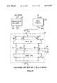
- FIG. 17shows one embodiment of the program circuit with inhibit 210 of FIG. 5 in more detail.
- the program circuit 210comprises N program with inhibit modules such as 801, 803. As illustrated in Table 1 and 2, in order to program the N cells, a voltage V PD must be applied to each of the N cells' drain and a voltage V PG applied to the control gates.
- Each program module such as 801serves to selectively pass V PD on a line 805 to one of the drains through the one of the N-channel data path 105. Since V PD is typically about 8 V to 9 V which is higher than V CC , the latter cannot be used to turn on the transistor switch 807. Rather the higher voltage V CG (about 12 V) is used to enable switch 807.
- V CG in line 801is itself enabled by an AND gate when both the program control signal PGM in line 813 is true and the signal in line 731 is a "0". Since the signal in line 731 is from the output of the cell compare module 701 shown in FIG. 16, it follows that V PD will be selectively passed onto those cells which are not yet verified. In this way, every time a programming pulse is applied, it is only applied to those cells which have not yet reached their intended states. This selective programming feature is especially necessary in implementing parallel programming and on chip verification in the multi-state case.
- FIG. 5The system diagram of FIG. 5 in conjunction with Tables 1 and 2 illustrate how various voltages are applied to the EEprom array 60 to perform the basic functions of the EEprom.
- Prior art EEprom devicesonly allow the voltage supplied to the control gate V CG to assume one of two voltages, namely V CC or the higher programming voltage of about 12 V.
- the voltage supplied to the control gate V CGis allowing to be independently and continuously variable over a wide range of voltages. This is provided by V PG from the controller 140.
- V CG in a line 83is fed from V PG which is in turn supplied by the controller from a line 901.
- Table 2shows V PG to assume various voltages under different functions of the EEprom.
- V CGvariability of V CG is particularly advantageous in program and erase margining schemes.
- program marginingthe read during program verify is done with V CG at a slightly higher voltage than the standard V CC . This helps to place the programmed threshold well into the state by programming past the breakpoint threshold level with a slight margin.
- erase verifythe cell is verified with a somewhat reduced V CG to put the cell well into the "erased" state.
- marginingcan be used to offset the charge retention problem described earlier (FIG. 8B).
- V CCAs mentioned before, prior art EEproms typically employ V CC to feed V CG during program or erase verify. In order to do margining, V CC itself needs to be ramped up or reduced. This practice produces inaccurate results in the reading circuits since they are also driven by V CC .
- V CGthe variability of V CG independent of voltages supplied to the reading circuit produce more accurate and reliable results.
- V CGis useful during testing and diagnostic of the EEprom. It allows the full range of the programmed cell's threshold to be measured easily by continuing to increase V CG (up to the maximum limited by the device's junction breakdown).
Landscapes
- Engineering & Computer Science (AREA)
- Computer Hardware Design (AREA)
- Read Only Memory (AREA)
- For Increasing The Reliability Of Semiconductor Memories (AREA)
Abstract
Description
Claims (47)
Priority Applications (11)
| Application Number | Priority Date | Filing Date | Title |
|---|---|---|---|
| US07508273US5172338B1 (en) | 1989-04-13 | 1990-04-11 | Multi-state eeprom read and write circuits and techniques |
| EP90906720AEP0539358B1 (en) | 1989-04-13 | 1990-04-12 | EEPROM including reference cell |
| PCT/US1990/001984WO1990012400A1 (en) | 1989-04-13 | 1990-04-12 | Multi-state eeprom read and write circuits and techniques |
| EP96114367AEP0774759B1 (en) | 1989-04-13 | 1990-04-12 | EEPROM having reference cells tracking charge leakage of memory cells |
| DE69033927TDE69033927T2 (en) | 1989-04-13 | 1990-04-12 | Memory sensing circuit using multi-current mirror circuit |
| DE69033862TDE69033862T2 (en) | 1989-04-13 | 1990-04-12 | Efficient parallel programming of data blocks in multi-state execution |
| DE69030959TDE69030959T2 (en) | 1989-04-13 | 1990-04-12 | EEPROM with reference cell |
| DE69033023TDE69033023T2 (en) | 1989-04-13 | 1990-04-12 | EEPROM with the charge losses of the memory cells following reference cells |
| EP96114368AEP0778582B1 (en) | 1989-04-13 | 1990-04-12 | Efficient parallel programming of data chunk in a multi-state implementation |
| EP96115502AEP0756287B1 (en) | 1989-04-13 | 1990-04-12 | A memory sensing circuit employing multi-current mirrors |
| JP2506478AJPH04507320A (en) | 1989-04-13 | 1990-04-12 | Multi-state EEPROM read/write circuit and technology |
Applications Claiming Priority (2)
| Application Number | Priority Date | Filing Date | Title |
|---|---|---|---|
| US33757989A | 1989-04-13 | 1989-04-13 | |
| US07508273US5172338B1 (en) | 1989-04-13 | 1990-04-11 | Multi-state eeprom read and write circuits and techniques |
Related Parent Applications (1)
| Application Number | Title | Priority Date | Filing Date |
|---|---|---|---|
| US33757989AContinuation-In-Part | 1989-04-13 | 1989-04-13 |
Related Child Applications (1)
| Application Number | Title | Priority Date | Filing Date |
|---|---|---|---|
| US07/734,221DivisionUS5163021A (en) | 1989-04-13 | 1991-07-22 | Multi-state EEprom read and write circuits and techniques |
Publications (2)
| Publication Number | Publication Date |
|---|---|
| US5172338Atrue US5172338A (en) | 1992-12-15 |
| US5172338B1 US5172338B1 (en) | 1997-07-08 |
Family
ID=26990766
Family Applications (1)
| Application Number | Title | Priority Date | Filing Date |
|---|---|---|---|
| US07508273Expired - LifetimeUS5172338B1 (en) | 1989-04-13 | 1990-04-11 | Multi-state eeprom read and write circuits and techniques |
Country Status (5)
| Country | Link |
|---|---|
| US (1) | US5172338B1 (en) |
| EP (4) | EP0774759B1 (en) |
| JP (1) | JPH04507320A (en) |
| DE (4) | DE69033927T2 (en) |
| WO (1) | WO1990012400A1 (en) |
Cited By (700)
| Publication number | Priority date | Publication date | Assignee | Title |
|---|---|---|---|---|
| US5270980A (en)* | 1991-10-28 | 1993-12-14 | Eastman Kodak Company | Sector erasable flash EEPROM |
| US5287317A (en)* | 1990-07-03 | 1994-02-15 | Mitsubishi Denki Kabushiki Kaisha | Non-volatile semiconductor memory device with over-erasing prevention |
| US5287326A (en)* | 1991-09-27 | 1994-02-15 | Nec Corporation | Non-volatile semiconductor memory device selectively skipping memory cells in programming |
| US5295255A (en)* | 1991-02-22 | 1994-03-15 | Electronic Professional Services, Inc. | Method and apparatus for programming a solid state processor with overleaved array memory modules |
| US5297096A (en)* | 1990-06-15 | 1994-03-22 | Mitsubishi Denki Kabushiki Kaisha | Nonvolatile semiconductor memory device and data erasing method thereof |
| US5357462A (en)* | 1991-09-24 | 1994-10-18 | Kabushiki Kaisha Toshiba | Electrically erasable and programmable non-volatile semiconductor memory with automatic write-verify controller |
| US5369647A (en)* | 1991-12-16 | 1994-11-29 | Intel Corporation | Circuitry and method for testing a write state machine |
| US5379256A (en)* | 1991-02-19 | 1995-01-03 | Kabushiki Kaisha Toshiba | Electrically erasable programmable read-only memory with write/verify controller |
| US5386388A (en)* | 1990-11-30 | 1995-01-31 | Intel Corporation | Single cell reference scheme for flash memory sensing and program state verification |
| US5388083A (en)* | 1993-03-26 | 1995-02-07 | Cirrus Logic, Inc. | Flash memory mass storage architecture |
| US5396458A (en)* | 1991-10-21 | 1995-03-07 | Rohm Co., Ltd. | Semiconductor memory device and method of writing and reading out information for the same |
| US5402370A (en)* | 1993-09-10 | 1995-03-28 | Intel Corporation | Circuitry and method for selecting a drain programming voltage for a nonvolatile memory |
| US5414829A (en)* | 1990-03-29 | 1995-05-09 | Intel Corporation | Override timing control circuitry and method for terminating program and erase sequences in a flash memory |
| US5430859A (en)* | 1991-07-26 | 1995-07-04 | Sundisk Corporation | Solid state memory system including plural memory chips and a serialized bus |
| US5440505A (en)* | 1994-01-21 | 1995-08-08 | Intel Corporation | Method and circuitry for storing discrete amounts of charge in a single memory element |
| US5446690A (en)* | 1993-08-10 | 1995-08-29 | Hitachi, Ltd. | Semiconductor nonvolatile memory device |
| US5448712A (en)* | 1991-02-11 | 1995-09-05 | Intel Corporation | Circuitry and method for programming and erasing a non-volatile semiconductor memory |
| US5450363A (en)* | 1994-06-02 | 1995-09-12 | Intel Corporation | Gray coding for a multilevel cell memory system |
| EP0675502A2 (en) | 1989-04-13 | 1995-10-04 | Sundisk Corporation | Multiple sector erase flash EEPROM system |
| US5457650A (en)* | 1993-07-12 | 1995-10-10 | Kabushiki Kaisha Toshiba | Apparatus and method for reading multi-level data stored in a semiconductor memory |
| US5457606A (en)* | 1993-11-10 | 1995-10-10 | Raymond Engineering Inc. | Hermetically sealed PC card unit including a header secured to a connector |
| US5479638A (en)* | 1993-03-26 | 1995-12-26 | Cirrus Logic, Inc. | Flash memory mass storage architecture incorporation wear leveling technique |
| US5485422A (en)* | 1994-06-02 | 1996-01-16 | Intel Corporation | Drain bias multiplexing for multiple bit flash cell |
| US5488711A (en)* | 1993-04-01 | 1996-01-30 | Microchip Technology Incorporated | Serial EEPROM device and associated method for reducing data load time using a page mode write cache |
| US5497354A (en)* | 1994-06-02 | 1996-03-05 | Intel Corporation | Bit map addressing schemes for flash memory |
| US5515324A (en)* | 1993-09-17 | 1996-05-07 | Kabushiki Kaisha Toshiba | EEPROM having NAND type memory cell array |
| US5515317A (en)* | 1994-06-02 | 1996-05-07 | Intel Corporation | Addressing modes for a dynamic single bit per cell to multiple bit per cell memory |
| US5519843A (en)* | 1993-03-15 | 1996-05-21 | M-Systems | Flash memory system providing both BIOS and user storage capability |
| US5521868A (en)* | 1993-08-11 | 1996-05-28 | Sony Corporation | NOR-type non-volatile memory using tunnel current and having selective re-write |
| US5530675A (en)* | 1993-04-01 | 1996-06-25 | Cypress Semiconductor Corp. | Floating gate nonvolatile memory with uniformly erased threshold voltage |
| US5532962A (en)* | 1992-05-20 | 1996-07-02 | Sandisk Corporation | Soft errors handling in EEPROM devices |
| US5537357A (en)* | 1994-06-27 | 1996-07-16 | Intel Corporation | Method for preconditioning a nonvolatile memory array |
| US5539690A (en)* | 1994-06-02 | 1996-07-23 | Intel Corporation | Write verify schemes for flash memory with multilevel cells |
| US5544103A (en)* | 1992-03-03 | 1996-08-06 | Xicor, Inc. | Compact page-erasable eeprom non-volatile memory |
| US5546561A (en)* | 1991-02-11 | 1996-08-13 | Intel Corporation | Circuitry and method for selectively protecting the integrity of data stored within a range of addresses within a non-volatile semiconductor memory |
| US5546351A (en)* | 1991-12-19 | 1996-08-13 | Kabushiki Kaisha Toshiba | Non-volatile semiconductor memory device and memory system using the same |
| US5559956A (en)* | 1992-01-10 | 1996-09-24 | Kabushiki Kaisha Toshiba | Storage system with a flash memory module |
| US5568424A (en)* | 1994-10-17 | 1996-10-22 | Sandisk Corporation | Programmable power generation circuit for flash EEPROM memory systems |
| US5596486A (en)* | 1993-11-10 | 1997-01-21 | Kaman Aerospace Corporation | Hermetically sealed memory or PC card unit having a frame, header and covers in bonded engagement |
| US5600593A (en)* | 1994-12-06 | 1997-02-04 | National Semiconductor Corporation | Apparatus and method for reducing erased threshold voltage distribution in flash memory arrays |
| US5610859A (en)* | 1994-03-15 | 1997-03-11 | Kabushiki Kaisha Toshiba | Semiconductor memory device |
| US5619448A (en)* | 1996-03-14 | 1997-04-08 | Myson Technology, Inc. | Non-volatile memory device and apparatus for reading a non-volatile memory array |
| US5638320A (en)* | 1994-11-02 | 1997-06-10 | Invoice Technology, Inc. | High resolution analog storage EPROM and flash EPROM |
| US5648930A (en)* | 1996-06-28 | 1997-07-15 | Symbios Logic Inc. | Non-volatile memory which is programmable from a power source |
| US5652719A (en)* | 1993-09-21 | 1997-07-29 | Kabushiki Kaisha Toshiba | Nonvolatile semiconductor memory device |
| US5657270A (en)* | 1990-03-31 | 1997-08-12 | Kabushiki Kaisha Toshiba | Electrically erasable programmable read-only memory with threshold value controller for data programming |
| US5657332A (en)* | 1992-05-20 | 1997-08-12 | Sandisk Corporation | Soft errors handling in EEPROM devices |
| US5661687A (en)* | 1996-09-30 | 1997-08-26 | Symbios Logic Inc. | Drain excluded EPROM cell |
| US5677869A (en)* | 1995-12-14 | 1997-10-14 | Intel Corporation | Programming flash memory using strict ordering of states |
| US5680341A (en)* | 1996-01-16 | 1997-10-21 | Invoice Technology | Pipelined record and playback for analog non-volatile memory |
| US5687114A (en)* | 1995-10-06 | 1997-11-11 | Agate Semiconductor, Inc. | Integrated circuit for storage and retrieval of multiple digital bits per nonvolatile memory cell |
| FR2749967A1 (en)* | 1996-06-13 | 1997-12-19 | Sgs Thomson Microelectronics | Memory cell reader for multiple level state memory |
| US5701266A (en)* | 1995-12-14 | 1997-12-23 | Intel Corporation | Programming flash memory using distributed learning methods |
| US5712815A (en)* | 1996-04-22 | 1998-01-27 | Advanced Micro Devices, Inc. | Multiple bits per-cell flash EEPROM capable of concurrently programming and verifying memory cells and reference cells |
| US5729489A (en)* | 1995-12-14 | 1998-03-17 | Intel Corporation | Programming flash memory using predictive learning methods |
| US5737265A (en)* | 1995-12-14 | 1998-04-07 | Intel Corporation | Programming flash memory using data stream analysis |
| US5742543A (en)* | 1996-08-19 | 1998-04-21 | Intel Corporation | Flash memory device having a page mode of operation |
| US5748546A (en)* | 1994-06-02 | 1998-05-05 | Intel Corporation | Sensing scheme for flash memory with multilevel cells |
| US5761110A (en)* | 1996-12-23 | 1998-06-02 | Lsi Logic Corporation | Memory cell capable of storing more than two logic states by using programmable resistances |
| US5764571A (en)* | 1991-02-08 | 1998-06-09 | Btg Usa Inc. | Electrically alterable non-volatile memory with N-bits per cell |
| US5771187A (en)* | 1996-12-23 | 1998-06-23 | Lsi Logic Corporation | Multiple level storage DRAM cell |
| US5776810A (en)* | 1992-01-14 | 1998-07-07 | Sandisk Corporation | Method for forming EEPROM with split gate source side injection |
| US5781478A (en)* | 1995-11-13 | 1998-07-14 | Kabushiki Kaisha Toshiba | Nonvolatile semiconductor memory device |
| US5784328A (en)* | 1996-12-23 | 1998-07-21 | Lsi Logic Corporation | Memory system including an on-chip temperature sensor for regulating the refresh rate of a DRAM array |
| US5787039A (en)* | 1997-03-06 | 1998-07-28 | Macronix International Co., Ltd. | Low current floating gate programming with bit-by-bit verification |
| US5798968A (en)* | 1996-09-24 | 1998-08-25 | Sandisk Corporation | Plane decode/virtual sector architecture |
| US5808932A (en)* | 1996-12-23 | 1998-09-15 | Lsi Logic Corporation | Memory system which enables storage and retrieval of more than two states in a memory cell |
| US5815436A (en)* | 1995-11-14 | 1998-09-29 | Kabushiki Kaisha Toshiba | Multi-level nonvolatile semiconductor memory device having improved programming level and read/write multi-level data circuits |
| US5815434A (en)* | 1995-09-29 | 1998-09-29 | Intel Corporation | Multiple writes per a single erase for a nonvolatile memory |
| US5838616A (en)* | 1996-09-30 | 1998-11-17 | Symbios, Inc. | Gate edge aligned EEPROM transistor |
| US5839108A (en)* | 1996-03-07 | 1998-11-17 | Norris Communications, Inc. | Flash memory file system in a handheld record and playback device |
| US5841695A (en)* | 1997-05-29 | 1998-11-24 | Lsi Logic Corporation | Memory system using multiple storage mechanisms to enable storage and retrieval of more than two states in a memory cell |
| US5847990A (en)* | 1996-12-23 | 1998-12-08 | Lsi Logic Corporation | Ram cell capable of storing 3 logic states |
| US5859796A (en)* | 1997-12-16 | 1999-01-12 | Advanced Micro Devices, Inc. | Programming of memory cells using connected floating gate analog reference cell |
| US5867429A (en)* | 1997-11-19 | 1999-02-02 | Sandisk Corporation | High density non-volatile flash memory without adverse effects of electric field coupling between adjacent floating gates |
| US5867423A (en)* | 1997-04-10 | 1999-02-02 | Lsi Logic Corporation | Memory circuit and method for multivalued logic storage by process variations |
| US5867417A (en)* | 1991-04-11 | 1999-02-02 | Sandisk Corporation | Computer memory cards using flash EEPROM integrated circuit chips and memory-controller systems |
| US5883409A (en)* | 1992-01-14 | 1999-03-16 | Sandisk Corporation | EEPROM with split gate source side injection |
| US5889697A (en)* | 1997-10-08 | 1999-03-30 | Advanced Micro Devices | Memory cell for storing at least three logic states |
| US5890192A (en)* | 1996-11-05 | 1999-03-30 | Sandisk Corporation | Concurrent write of multiple chunks of data into multiple subarrays of flash EEPROM |
| US5892715A (en)* | 1996-07-30 | 1999-04-06 | Nec Corporation | Non-volatile semiconductor memory device with variable source voltage |
| US5901089A (en)* | 1996-04-30 | 1999-05-04 | Agate Semiconductor, Inc. | Stabilization circuits and techniques for storage and retrieval of single or multiple digital bits per memory cell |
| US5909404A (en)* | 1998-03-27 | 1999-06-01 | Lsi Logic Corporation | Refresh sampling built-in self test and repair circuit |
| US5912844A (en)* | 1998-01-28 | 1999-06-15 | Macronix International Co., Ltd. | Method for flash EEPROM data writing |
| US5930167A (en)* | 1997-07-30 | 1999-07-27 | Sandisk Corporation | Multi-state non-volatile flash memory capable of being its own two state write cache |
| US5956268A (en)* | 1997-02-12 | 1999-09-21 | Hyundai Electronics America | Nonvolatile memory structure |
| US5956350A (en)* | 1997-10-27 | 1999-09-21 | Lsi Logic Corporation | Built in self repair for DRAMs using on-chip temperature sensing and heating |
| US5969986A (en)* | 1998-06-23 | 1999-10-19 | Invox Technology | High-bandwidth read and write architectures for non-volatile memories |
| US5982659A (en)* | 1996-12-23 | 1999-11-09 | Lsi Logic Corporation | Memory cell capable of storing more than two logic states by using different via resistances |
| US5987563A (en)* | 1992-02-20 | 1999-11-16 | Fujitsu Limited | Flash memory accessed using only the logical address |
| US5991206A (en)* | 1997-12-10 | 1999-11-23 | Hyundai Electronics Industries Co., Ltd. | Method of erasing a flash memory |
| US5996108A (en)* | 1993-12-28 | 1999-11-30 | Kabushiki Kaisha Toshiba | Memory system |
| EP0962940A1 (en)* | 1998-05-19 | 1999-12-08 | Nec Corporation | Method and apparatus capable of trimming a nonvolatile semiconductor storage device without any superfluous pads or terminals |
| US6002614A (en)* | 1991-02-08 | 1999-12-14 | Btg International Inc. | Memory apparatus including programmable non-volatile multi-bit memory cell, and apparatus and method for demarcating memory states of the cell |
| US6002605A (en)* | 1997-02-28 | 1999-12-14 | Kabushiki Kaisha Toshiba | Connecting apparatus, and information processing apparatus |
| US6005895A (en)* | 1996-12-20 | 1999-12-21 | Rambus Inc. | Apparatus and method for multilevel signaling |
| EP0967617A1 (en)* | 1998-06-22 | 1999-12-29 | Texas Instruments Incorporated | A floating gate transistor, multi-level cell memory device and method for programming the cells and stabilizing the programmed charge |
| US6011725A (en)* | 1997-08-01 | 2000-01-04 | Saifun Semiconductors, Ltd. | Two bit non-volatile electrically erasable and programmable semiconductor memory cell utilizing asymmetrical charge trapping |
| US6031760A (en)* | 1997-07-29 | 2000-02-29 | Kabushiki Kaisha Toshiba | Semiconductor memory device and method of programming the same |
| US6031724A (en)* | 1994-11-29 | 2000-02-29 | Kabushiki Kaisha Toshiba | IC card and method of manufacturing the same |
| US6038169A (en)* | 1999-03-18 | 2000-03-14 | Halo Lsi Design & Device Technology, Inc. | Read reference scheme for flash memory |
| US6038165A (en)* | 1995-01-31 | 2000-03-14 | Hitachi, Ltd. | Nonvolatile memory device and refreshing method |
| US6038166A (en)* | 1998-04-01 | 2000-03-14 | Invox Technology | High resolution multi-bit-per-cell memory |
| US6040997A (en)* | 1998-03-25 | 2000-03-21 | Lexar Media, Inc. | Flash memory leveling architecture having no external latch |
| US6044019A (en)* | 1998-10-23 | 2000-03-28 | Sandisk Corporation | Non-volatile memory with improved sensing and method therefor |
| US6054774A (en)* | 1994-03-22 | 2000-04-25 | Kabushiki Kaisha Toshiba | Thin type semiconductor package |
| US6081447A (en)* | 1991-09-13 | 2000-06-27 | Western Digital Corporation | Wear leveling techniques for flash EEPROM systems |
| US6084797A (en)* | 1998-03-27 | 2000-07-04 | Stmicroelectronics S.R.L. | Method for reading a multiple-level memory cell |
| US6085412A (en)* | 1996-06-11 | 2000-07-11 | Kabushiki Kaisha Toshiba | Method for manufacturing card type memory device |
| US6091137A (en)* | 1996-05-31 | 2000-07-18 | Kabushiki Kaisha Toshiba | Semiconductor device substrate and method of manufacturing the same |
| US6091633A (en)* | 1999-08-09 | 2000-07-18 | Sandisk Corporation | Memory array architecture utilizing global bit lines shared by multiple cells |
| US6094697A (en)* | 1995-02-03 | 2000-07-25 | Kabuhiki Kaisha Toshiba | Information processing system including processing device for detecting non-conductivity of state-indicating non-conductive member and discriminating prohibit state of writing information to information writable storage medium |
| US6097637A (en)* | 1994-06-02 | 2000-08-01 | Intel Corporation | Dynamic single bit per cell to multiple bit per cell memory |
| US6103573A (en)* | 1999-06-30 | 2000-08-15 | Sandisk Corporation | Processing techniques for making a dual floating gate EEPROM cell array |
| US6141253A (en)* | 1997-08-26 | 2000-10-31 | Macronix International Co., Ltd. | Electrically programmable semiconductor device with concurrent program and verification operations |
| US6151248A (en)* | 1999-06-30 | 2000-11-21 | Sandisk Corporation | Dual floating gate EEPROM cell array with steering gates shared by adjacent cells |
| US6166950A (en)* | 1996-07-10 | 2000-12-26 | Hitachi, Ltd. | Nonvolatile semiconductor storage device |
| US6166431A (en)* | 1995-08-25 | 2000-12-26 | Kabushiki Kaisha Tishiba | Semiconductor device with a thickness of 1 MM or less |
| US6178118B1 (en) | 1997-08-26 | 2001-01-23 | Macronix International Co., Ltd. | Electrically programmable semiconductor device with multi-level wordline voltages for programming multi-level threshold voltages |
| US6181603B1 (en) | 1996-05-01 | 2001-01-30 | Hitachi, Ltd. | Nonvolatile semiconductor memory device having plural memory cells which store multi-value information |
| US6201295B1 (en) | 1993-04-28 | 2001-03-13 | Kabushiki Kaisha Toshiba | Plate-shaped external storage device and method of producing the same |
| US6202138B1 (en) | 1995-07-31 | 2001-03-13 | Lexar Media, Inc | Increasing the memory performance of flash memory devices by writing sectors simultaneously to multiple flash memory devices |
| US6208770B1 (en) | 1998-09-18 | 2001-03-27 | Eastman Kodak Company | Digital colored corrected prints produced from colored film |
| US6208560B1 (en)* | 1997-05-14 | 2001-03-27 | Kabushiki Kaisha Toshiba | Nonvolatile semiconductor memory device |
| US6222762B1 (en)* | 1992-01-14 | 2001-04-24 | Sandisk Corporation | Multi-state memory |
| US6243298B1 (en) | 1999-08-19 | 2001-06-05 | Azalea Microelectronics Corporation | Non-volatile memory cell capable of being programmed and erased through substantially separate areas of one of its drain-side and source-side regions |
| US6266724B1 (en)* | 1993-09-01 | 2001-07-24 | Sandisk Corporation | Removable mother/daughter peripheral card |
| US6281075B1 (en) | 1999-01-27 | 2001-08-28 | Sandisk Corporation | Method of controlling of floating gate oxide growth by use of an oxygen barrier |
| US6282145B1 (en) | 1999-01-14 | 2001-08-28 | Silicon Storage Technology, Inc. | Array architecture and operating methods for digital multilevel nonvolatile memory integrated circuit system |
| US6285615B1 (en) | 2000-06-09 | 2001-09-04 | Sandisk Corporation | Multiple output current mirror with improved accuracy |
| US6285574B1 (en) | 1997-12-12 | 2001-09-04 | Saifun Semiconductors Ltd. | Symmetric segmented memory array architecture |
| US6285598B1 (en) | 1997-03-06 | 2001-09-04 | Silicon Storage Technology, Inc. | Precision programming of nonvolatile memory cells |
| US6288938B1 (en) | 1999-08-19 | 2001-09-11 | Azalea Microelectronics Corporation | Flash memory architecture and method of operation |
| US6292394B1 (en) | 2000-06-29 | 2001-09-18 | Saifun Semiconductors Ltd. | Method for programming of a semiconductor memory cell |
| US6292397B1 (en) | 1999-06-16 | 2001-09-18 | Hyundai Electronics Industries Co., Ltd. | Nonvolatile memory sensing circuit and techniques thereof |
| US6297096B1 (en) | 1997-06-11 | 2001-10-02 | Saifun Semiconductors Ltd. | NROM fabrication method |
| US6314025B1 (en) | 1998-06-23 | 2001-11-06 | Sandisk Corporation | High data rate write process for non-volatile flash memories |
| US6327181B1 (en)* | 1999-10-19 | 2001-12-04 | Advanced Micro Devices Inc. | Reference cell bitline path architecture for a simultaneous operation flash memory device |
| US6331960B1 (en) | 1995-09-13 | 2001-12-18 | Kabushiki Kaisha Toshiba | Nonvolatile semiconductor memory device and method for using the same |
| US6335878B1 (en) | 1998-07-28 | 2002-01-01 | Hitachi, Ltd. | Non-volatile multi-level semiconductor flash memory device and method of driving same |
| US6345001B1 (en) | 2000-09-14 | 2002-02-05 | Sandisk Corporation | Compressed event counting technique and application to a flash memory system |
| US6353554B1 (en) | 1995-02-27 | 2002-03-05 | Btg International Inc. | Memory apparatus including programmable non-volatile multi-bit memory cell, and apparatus and method for demarcating memory states of the cell |
| US6363008B1 (en) | 2000-02-17 | 2002-03-26 | Multi Level Memory Technology | Multi-bit-cell non-volatile memory with maximized data capacity |
| US6374337B1 (en) | 1998-11-17 | 2002-04-16 | Lexar Media, Inc. | Data pipelining method and apparatus for memory control circuit |
| US6396742B1 (en) | 2000-07-28 | 2002-05-28 | Silicon Storage Technology, Inc. | Testing of multilevel semiconductor memory |
| US6396741B1 (en) | 2000-05-04 | 2002-05-28 | Saifun Semiconductors Ltd. | Programming of nonvolatile memory cells |
| US6396329B1 (en) | 1999-10-19 | 2002-05-28 | Rambus, Inc | Method and apparatus for receiving high speed signals with low latency |
| US6396744B1 (en) | 2000-04-25 | 2002-05-28 | Multi Level Memory Technology | Flash memory with dynamic refresh |
| US6411546B1 (en) | 1997-03-31 | 2002-06-25 | Lexar Media, Inc. | Nonvolatile memory using flexible erasing methods and method and system for using same |
| US6414893B1 (en) | 1995-09-13 | 2002-07-02 | Kabushiki Kaisha Toshiba | Nonvolatile semiconductor memory device and method of using the same |
| US6426893B1 (en) | 2000-02-17 | 2002-07-30 | Sandisk Corporation | Flash eeprom system with simultaneous multiple data sector programming and storage of physical block characteristics in other designated blocks |
| US6430077B1 (en) | 1997-12-12 | 2002-08-06 | Saifun Semiconductors Ltd. | Method for regulating read voltage level at the drain of a cell in a symmetric array |
| US20020118574A1 (en)* | 2001-02-26 | 2002-08-29 | Geoffrey Gongwer | Non-volatile memory with improved programming and method therefor |
| US6448750B1 (en) | 2001-04-05 | 2002-09-10 | Saifun Semiconductor Ltd. | Voltage regulator for non-volatile memory with large power supply rejection ration and minimal current drain |
| US6456528B1 (en) | 2001-09-17 | 2002-09-24 | Sandisk Corporation | Selective operation of a multi-state non-volatile memory system in a binary mode |
| EP1248263A1 (en)* | 2001-04-05 | 2002-10-09 | Saifun Semiconductors Ltd | Method for programming a reference cell |
| US6466476B1 (en) | 2001-01-18 | 2002-10-15 | Multi Level Memory Technology | Data coding for multi-bit-per-cell memories having variable numbers of bits per memory cell |
| US6471130B2 (en) | 1995-02-03 | 2002-10-29 | Kabushiki Kaisha Toshiba | Information storage apparatus and information processing apparatus using the same |
| US6480422B1 (en) | 2001-06-14 | 2002-11-12 | Multi Level Memory Technology | Contactless flash memory with shared buried diffusion bit line architecture |
| US6487116B2 (en) | 1997-03-06 | 2002-11-26 | Silicon Storage Technology, Inc. | Precision programming of nonvolatile memory cells |
| US6490204B2 (en) | 2000-05-04 | 2002-12-03 | Saifun Semiconductors Ltd. | Programming and erasing methods for a reference cell of an NROM array |
| US6490200B2 (en) | 2000-03-27 | 2002-12-03 | Sandisk Corporation | Non-volatile memory with improved sensing and method therefor |
| US20020184268A1 (en)* | 2001-05-30 | 2002-12-05 | International Business Machines Corporation | Method of changing service attributes in a service logic execution environment |
| US6501684B1 (en) | 1999-09-24 | 2002-12-31 | Azalea Microelectronics Corporation | Integrated circuit having an EEPROM and flash EPROM |
| US6512263B1 (en) | 2000-09-22 | 2003-01-28 | Sandisk Corporation | Non-volatile memory cell array having discontinuous source and drain diffusions contacted by continuous bit line conductors and methods of forming |
| US20030021149A1 (en)* | 1997-09-08 | 2003-01-30 | So Hock C. | Multi-bit-per-cell flash EEPROM memory with refresh |
| US20030028699A1 (en)* | 2001-08-02 | 2003-02-06 | Michael Holtzman | Removable computer with mass storage |
| US6522580B2 (en)* | 2001-06-27 | 2003-02-18 | Sandisk Corporation | Operating techniques for reducing effects of coupling between storage elements of a non-volatile memory operated in multiple data states |
| US6522585B2 (en) | 2001-05-25 | 2003-02-18 | Sandisk Corporation | Dual-cell soft programming for virtual-ground memory arrays |
| WO2003015173A2 (en) | 2001-08-08 | 2003-02-20 | Sandisk Corporation | Floating gate memory array and methods of forming |
| US6529405B2 (en) | 2000-12-30 | 2003-03-04 | Hynix Semiconductor, Inc. | Circuit and method for programming and reading multi-level flash memory |
| US6532556B1 (en) | 2000-01-27 | 2003-03-11 | Multi Level Memory Technology | Data management for multi-bit-per-cell memories |
| US6538922B1 (en) | 2000-09-27 | 2003-03-25 | Sandisk Corporation | Writable tracking cells |
| US6542407B1 (en) | 2002-01-18 | 2003-04-01 | Sandisk Corporation | Techniques of recovering data from memory cells affected by field coupling with adjacent memory cells |
| US6545912B1 (en)* | 2000-04-25 | 2003-04-08 | Advanced Micro Devices, Inc. | Erase verify mode to evaluate negative Vt's |
| US6552932B1 (en) | 2001-09-21 | 2003-04-22 | Sandisk Corporation | Segmented metal bitlines |
| US6552387B1 (en) | 1997-07-30 | 2003-04-22 | Saifun Semiconductors Ltd. | Non-volatile electrically erasable and programmable semiconductor memory cell utilizing asymmetrical charge trapping |
| US6560152B1 (en) | 2001-11-02 | 2003-05-06 | Sandisk Corporation | Non-volatile memory with temperature-compensated data read |
| US6560146B2 (en) | 2001-09-17 | 2003-05-06 | Sandisk Corporation | Dynamic column block selection |
| US6570785B1 (en) | 2000-10-31 | 2003-05-27 | Sandisk Corporation | Method of reducing disturbs in non-volatile memory |
| US6577535B2 (en) | 2001-02-16 | 2003-06-10 | Sandisk Corporation | Method and system for distributed power generation in multi-chip memory systems |
| US20030109093A1 (en)* | 2001-10-31 | 2003-06-12 | Eliyahou Harari | Multi-state non-volatile integrated circuit memory systems that employ dielectric storage elements |
| US6584017B2 (en) | 2001-04-05 | 2003-06-24 | Saifun Semiconductors Ltd. | Method for programming a reference cell |
| US6583007B1 (en) | 2001-12-20 | 2003-06-24 | Saifun Semiconductors Ltd. | Reducing secondary injection effects |
| US20030135470A1 (en)* | 2002-01-16 | 2003-07-17 | Beard Robert E. | Method and system for credit card purchases |
| US6601140B1 (en)* | 1999-04-07 | 2003-07-29 | Sony Corporation | Memory unit, data processing unit, and data processing method using memory unit type |
| US6606267B2 (en) | 1998-06-23 | 2003-08-12 | Sandisk Corporation | High data rate write process for non-volatile flash memories |
| US6614692B2 (en) | 2001-01-18 | 2003-09-02 | Saifun Semiconductors Ltd. | EEPROM array and method for operation thereof |
| WO2003073290A1 (en) | 2002-02-22 | 2003-09-04 | Sandisk Corporation | Pipelined parallel programming operation in a non-volatile memory system |
| US6621739B2 (en) | 2002-01-18 | 2003-09-16 | Sandisk Corporation | Reducing the effects of noise in non-volatile memories through multiple reads |
| US6633499B1 (en) | 1997-12-12 | 2003-10-14 | Saifun Semiconductors Ltd. | Method for reducing voltage drops in symmetric array architectures |
| US6633496B2 (en) | 1997-12-12 | 2003-10-14 | Saifun Semiconductors Ltd. | Symmetric architecture for memory cells having widely spread metal bit lines |
| US6636440B2 (en) | 2001-04-25 | 2003-10-21 | Saifun Semiconductors Ltd. | Method for operation of an EEPROM array, including refresh thereof |
| US6643181B2 (en) | 2001-10-24 | 2003-11-04 | Saifun Semiconductors Ltd. | Method for erasing a memory cell |
| US6642611B2 (en)* | 1998-03-26 | 2003-11-04 | Kabushiki Kaisha Toshiba | Storage apparatus, card type storage apparatus, and electronic apparatus |
| US6646922B2 (en) | 2001-05-31 | 2003-11-11 | Semiconductor Energy Laboratory Co., Ltd. | Nonvolatile memory and method of driving the same |
| US20030209751A1 (en)* | 2001-05-18 | 2003-11-13 | Sandisk Corporation | Floating gate memory cells utilizing substrate trenches to scale down their size |
| US6662263B1 (en) | 2000-03-03 | 2003-12-09 | Multi Level Memory Technology | Sectorless flash memory architecture |
| US6664587B2 (en) | 1996-02-28 | 2003-12-16 | Sandisk Corporation | EEPROM cell array structure with specific floating gate shape |
| US20040000688A1 (en)* | 2001-05-18 | 2004-01-01 | Sandisk Corporation | Non-volatile memory cells utilizing substrate trenches |
| US6677805B2 (en) | 2001-04-05 | 2004-01-13 | Saifun Semiconductors Ltd. | Charge pump stage with body effect minimization |
| US6678192B2 (en) | 2001-11-02 | 2004-01-13 | Sandisk Corporation | Error management for writable tracking storage units |
| US6684289B1 (en) | 2000-11-22 | 2004-01-27 | Sandisk Corporation | Techniques for operating non-volatile memory systems with data sectors having different sizes than the sizes of the pages and/or blocks of the memory |
| US20040022311A1 (en)* | 2002-07-12 | 2004-02-05 | Zerbe Jared L. | Selectable-tap equalizer |
| US20040027865A1 (en)* | 2000-10-31 | 2004-02-12 | Mangan John S. | Method of reducing disturbs in non-volatile memory |
| US6707713B1 (en)* | 2000-03-01 | 2004-03-16 | Advanced Micro Devices, Inc. | Interlaced multi-level memory |
| US20040057318A1 (en)* | 2002-09-24 | 2004-03-25 | Sandisk Corporation | Non-volatile memory and method with reduced bit line crosstalk errors |
| US20040057285A1 (en)* | 2002-09-24 | 2004-03-25 | Sandisk Corporation | Non-volatile memory and method with reduced neighboring field errors |
| US20040060031A1 (en)* | 2002-09-24 | 2004-03-25 | Sandisk Corporation | Highly compact non-volatile memory and method thereof |
| EP1211692A3 (en)* | 1997-11-21 | 2004-03-31 | BTG International Inc | Memory apparatus including programmable non-volatile multi-bit memory cell, and apparatus and method for demarcating memory states of the cell |
| US6717847B2 (en) | 2001-09-17 | 2004-04-06 | Sandisk Corporation | Selective operation of a multi-state non-volatile memory system in a binary mode |
| US20040070021A1 (en)* | 2002-10-09 | 2004-04-15 | Yuan Jack H. | Flash memory array with increased coupling between floating and control gates |
| US6728851B1 (en) | 1995-07-31 | 2004-04-27 | Lexar Media, Inc. | Increasing the memory performance of flash memory devices by writing sectors simultaneously to multiple flash memory devices |
| US20040083335A1 (en)* | 2002-10-28 | 2004-04-29 | Gonzalez Carlos J. | Automated wear leveling in non-volatile storage systems |
| US6741502B1 (en) | 2001-09-17 | 2004-05-25 | Sandisk Corporation | Background operation for memory cells |
| US6747892B2 (en) | 2000-11-21 | 2004-06-08 | Sandisk Corporation | Sense amplifier for multilevel non-volatile integrated memory devices |
| US6747896B2 (en) | 2002-05-06 | 2004-06-08 | Multi Level Memory Technology | Bi-directional floating gate nonvolatile memory |
| US20040109353A1 (en)* | 2002-12-04 | 2004-06-10 | Sharp Kabushiki Kaisha | Semiconductor memory device and method for correcting a reference cell |
| US20040109357A1 (en)* | 2002-09-24 | 2004-06-10 | Raul-Adrian Cernea | Non-volatile memory and method with improved sensing |
| EP1271550A3 (en)* | 2001-06-20 | 2004-06-23 | Fujitsu Limited | Method and device for reading dual bit memory cells using multiple reference cells with two side read |
| US6757800B1 (en) | 1995-07-31 | 2004-06-29 | Lexar Media, Inc. | Increasing the memory performance of flash memory devices by writing sectors simultaneously to multiple flash memory devices |
| US6763424B2 (en) | 2001-01-19 | 2004-07-13 | Sandisk Corporation | Partial block data programming and reading operations in a non-volatile memory |
| US20040145952A1 (en)* | 2003-01-28 | 2004-07-29 | Jian Chen | Non-volatile semiconductor memory with large erase blocks storing cycle counts |
| US6781895B1 (en) | 1991-12-19 | 2004-08-24 | Kabushiki Kaisha Toshiba | Non-volatile semiconductor memory device and memory system using the same |
| US6781877B2 (en) | 2002-09-06 | 2004-08-24 | Sandisk Corporation | Techniques for reducing effects of coupling between storage elements of adjacent rows of memory cells |
| US20040165443A1 (en)* | 2002-10-28 | 2004-08-26 | Eliyahou Harari | Flash memory cell arrays having dual control gates per memory cell charge storage element |
| US20040179404A1 (en)* | 2001-12-18 | 2004-09-16 | Quader Khandker N. | Method and system for programming and inhibiting multi-level, non-volatile memory cells |
| US20040190347A1 (en)* | 2001-09-17 | 2004-09-30 | Raul-Adrian Cernea | Dynamic column block selection |
| US6801979B1 (en) | 1995-07-31 | 2004-10-05 | Lexar Media, Inc. | Method and apparatus for memory control circuit |
| US20040205290A1 (en)* | 2003-04-10 | 2004-10-14 | Renesas Technology Corp. | Memory device |
| US20040228197A1 (en)* | 2000-09-14 | 2004-11-18 | Nima Mokhlesi | Compressed event counting technique and application to a flash memory system |
| US20040232496A1 (en)* | 2003-05-21 | 2004-11-25 | Jian Chen | Use of voids between elements in semiconductor structures for isolation |
| US6826107B2 (en) | 2002-08-01 | 2004-11-30 | Saifun Semiconductors Ltd. | High voltage insertion in flash memory cards |
| US20040240269A1 (en)* | 2001-09-17 | 2004-12-02 | Raul-Adrian Cernea | Latched programming of memory and method |
| US20040255090A1 (en)* | 2003-06-13 | 2004-12-16 | Guterman Daniel C. | Tracking cells for a memory system |
| US20040266107A1 (en)* | 2003-06-27 | 2004-12-30 | Chindalore Gowrishankar L. | Non-volatile memory having a reference transistor and method for forming |
| US6839280B1 (en) | 2003-06-27 | 2005-01-04 | Freescale Semiconductor, Inc. | Variable gate bias for a reference transistor in a non-volatile memory |
| US20050003616A1 (en)* | 2003-06-20 | 2005-01-06 | Jeffrey Lutze | Self aligned non-volatile memory cell and process for fabrication |
| US20050007801A1 (en)* | 2001-09-17 | 2005-01-13 | Ron Barzilai | Multi-purpose non-volatile memory card |
| US6850441B2 (en) | 2002-01-18 | 2005-02-01 | Sandisk Corporation | Noise reduction technique for transistors and small devices utilizing an episodic agitation |
| US6856568B1 (en) | 2000-04-25 | 2005-02-15 | Multi Level Memory Technology | Refresh operations that change address mappings in a non-volatile memory |
| US20050057965A1 (en)* | 2003-09-17 | 2005-03-17 | Raul-Adrian Cernea | Non-volatile memory and method with bit line coupled compensation |
| US20050057967A1 (en)* | 2003-09-17 | 2005-03-17 | Shahzad Khalid | Non-volatile memory and method with bit line compensation dependent on neighboring operating modes |
| US20050057953A1 (en)* | 2003-09-16 | 2005-03-17 | Eli Lusky | Reading array cell with matched reference cell |
| US20050063236A1 (en)* | 2003-08-06 | 2005-03-24 | Stmicroelectronics S.R.I | Sense amplifier |
| US20050073884A1 (en)* | 2003-10-03 | 2005-04-07 | Gonzalez Carlos J. | Flash memory data correction and scrub techniques |
| US20050072999A1 (en)* | 2003-10-06 | 2005-04-07 | George Matamis | Bitline direction shielding to avoid cross coupling between adjacent cells for NAND flash memory |
| US6885585B2 (en) | 2001-12-20 | 2005-04-26 | Saifun Semiconductors Ltd. | NROM NOR array |
| US6891753B2 (en) | 2002-09-24 | 2005-05-10 | Sandisk Corporation | Highly compact non-volatile memory and method therefor with internal serial buses |
| US6893268B1 (en) | 1993-09-01 | 2005-05-17 | Sandisk Corporation | Removable mother/daughter peripheral card |
| US6894930B2 (en) | 2002-06-19 | 2005-05-17 | Sandisk Corporation | Deep wordline trench to shield cross coupling between adjacent cells for scaled NAND |
| US6897522B2 (en) | 2001-10-31 | 2005-05-24 | Sandisk Corporation | Multi-state non-volatile integrated circuit memory systems that employ dielectric storage elements |
| US6901498B2 (en) | 2002-12-09 | 2005-05-31 | Sandisk Corporation | Zone boundary adjustment for defects in non-volatile memories |
| US20050135154A1 (en)* | 2001-12-27 | 2005-06-23 | Kabushiki Kaisha Toshiba | Nonvolatile semiconductor memory adapted to store a multi-valued data in a single memory cell |
| US20050144367A1 (en)* | 2003-12-30 | 2005-06-30 | Sinclair Alan W. | Data run programming |
| US20050141387A1 (en)* | 2003-12-31 | 2005-06-30 | Raul-Adrian Cernea | Flexible and area efficient column redundancy for non-volatile memories |
| US20050144358A1 (en)* | 2003-12-30 | 2005-06-30 | Conley Kevin M. | Management of non-volatile memory systems having large erase blocks |
| US20050144357A1 (en)* | 2003-12-30 | 2005-06-30 | Sinclair Alan W. | Adaptive metablocks |
| US20050144363A1 (en)* | 2003-12-30 | 2005-06-30 | Sinclair Alan W. | Data boundary management |
| US6914820B1 (en) | 2002-05-06 | 2005-07-05 | Multi Level Memory Technology | Erasing storage nodes in a bi-directional nonvolatile memory cell |
| US20050157549A1 (en)* | 2004-01-21 | 2005-07-21 | Nima Mokhlesi | Non-volatile memory cell using high-k material and inter-gate programming |
| US20050166087A1 (en)* | 2003-12-30 | 2005-07-28 | Gorobets Sergey A. | Non-volatile memory and method with phased program failure handling |
| US20050162927A1 (en)* | 2002-06-19 | 2005-07-28 | Henry Chien | Deep wordline trench to shield cross coupling between adjacent cells for scaled NAND |
| US20050169082A1 (en)* | 2002-09-24 | 2005-08-04 | Raul-Adrian Cernea | Memory sensing circuit and method for low voltage operation |
| US6928001B2 (en) | 2000-12-07 | 2005-08-09 | Saifun Semiconductors Ltd. | Programming and erasing methods for a non-volatile memory cell |
| US20050180186A1 (en)* | 2004-02-13 | 2005-08-18 | Lutze Jeffrey W. | Shield plate for limiting cross coupling between floating gates |
| US6937495B2 (en) | 2001-03-21 | 2005-08-30 | Matrix Semiconductor, Inc. | Current sensing method and apparatus particularly useful for a memory array of cells having diode-like characteristics |
| US6940753B2 (en) | 2002-09-24 | 2005-09-06 | Sandisk Corporation | Highly compact non-volatile memory and method therefor with space-efficient data registers |
| US20050195635A1 (en)* | 2004-03-08 | 2005-09-08 | Conley Kevin M. | Flash controller cache architecture |
| US20050199939A1 (en)* | 2004-03-12 | 2005-09-15 | Lutze Jeffrey W. | Self aligned non-volatile memory cells and processes for fabrication |
| US20050237814A1 (en)* | 2004-04-23 | 2005-10-27 | Sandisk Corporation | Non-volatile memory and control with improved partial page program capability |
| US6963505B2 (en) | 2002-10-29 | 2005-11-08 | Aifun Semiconductors Ltd. | Method circuit and system for determining a reference voltage |
| US20050265081A1 (en)* | 2004-05-28 | 2005-12-01 | Dat Tran | Comprehensive erase verification for non-volatile memory |
| US6980471B1 (en) | 2004-12-23 | 2005-12-27 | Sandisk Corporation | Substrate electron injection techniques for programming non-volatile charge storage memory cells |
| US20060020745A1 (en)* | 2004-07-21 | 2006-01-26 | Conley Kevin M | Fat analysis for optimized sequential cluster management |
| US20060020744A1 (en)* | 2004-07-21 | 2006-01-26 | Sandisk Corporation | Method and apparatus for maintaining data on non-volatile memory systems |
| US6992932B2 (en) | 2002-10-29 | 2006-01-31 | Saifun Semiconductors Ltd | Method circuit and system for read error detection in a non-volatile memory array |
| US20060031593A1 (en)* | 2004-08-09 | 2006-02-09 | Sinclair Alan W | Ring bus structure and its use in flash memory systems |
| USRE38997E1 (en)* | 1995-02-03 | 2006-02-28 | Kabushiki Kaisha Toshiba | Information storage and information processing system utilizing state-designating member provided on supporting card surface which produces write-permitting or write-inhibiting signal |
| US20060050562A1 (en)* | 2002-09-24 | 2006-03-09 | Raul-Adrian Cernea | Non-volatile memory and method with improved sensing |
| US20060067181A1 (en)* | 1999-05-08 | 2006-03-30 | Samsung Electronics Co., Ltd | Recording medium for storing linking type information and method of processing defective area using the same |
| US20060106972A1 (en)* | 2004-11-15 | 2006-05-18 | Gorobets Sergey A | Cyclic flash memory wear leveling |
| US20060110880A1 (en)* | 2004-11-23 | 2006-05-25 | Yuan Jack H | Self-aligned trench filling with high coupling ratio |
| US20060108648A1 (en)* | 2004-11-23 | 2006-05-25 | Yuan Jack H | Memory with self-aligned trenches for narrow gap isolation regions |
| US20060126391A1 (en)* | 2004-12-09 | 2006-06-15 | Bo-Geun Kim | Methods of program verifying non-volatile memory devices |
| US20060126393A1 (en)* | 2004-12-14 | 2006-06-15 | Yan Li | Data recovery methods in multi-state memory after program fail |
| US20060136656A1 (en)* | 2004-12-21 | 2006-06-22 | Conley Kevin M | System and method for use of on-chip non-volatile memory write cache |
| US20060132114A1 (en)* | 2004-12-21 | 2006-06-22 | Hari Giduturi | Step voltage generation |
| US20060134864A1 (en)* | 2004-12-22 | 2006-06-22 | Masaaki Higashitani | Multi-thickness dielectric for semiconductor memory |
| US20060134845A1 (en)* | 2004-12-22 | 2006-06-22 | Tuan Pham | Low-voltage, multiple thin-gate oxide and low-resistance gate electrode |
| US20060136655A1 (en)* | 2004-12-16 | 2006-06-22 | Gorobets Sergey A | Cluster auto-alignment |
| US20060140007A1 (en)* | 2004-12-29 | 2006-06-29 | Raul-Adrian Cernea | Non-volatile memory and method with shared processing for an aggregate of read/write circuits |
| US20060155922A1 (en)* | 2004-12-16 | 2006-07-13 | Gorobets Sergey A | Non-volatile memory and method with improved indexing for scratch pad and update blocks |
| US20060155920A1 (en)* | 2004-12-16 | 2006-07-13 | Smith Peter J | Non-volatile memory and method with multi-stream updating |
| US20060155921A1 (en)* | 2004-12-16 | 2006-07-13 | Gorobets Sergey A | Non-volatile memory and method with multi-stream update tracking |
| US7079422B1 (en) | 2000-04-25 | 2006-07-18 | Samsung Electronics Co., Ltd. | Periodic refresh operations for non-volatile multiple-bit-per-cell memory |
| US20060161724A1 (en)* | 2005-01-20 | 2006-07-20 | Bennett Alan D | Scheduling of housekeeping operations in flash memory systems |
| US20060161728A1 (en)* | 2005-01-20 | 2006-07-20 | Bennett Alan D | Scheduling of housekeeping operations in flash memory systems |
| US20060158947A1 (en)* | 2002-09-24 | 2006-07-20 | Chan Siu L | Reference sense amplifier for non-volatile memory |
| US20060158935A1 (en)* | 2002-09-24 | 2006-07-20 | Chan Siu L | Method for compensated sensing in non-volatile memory |
| US7093145B2 (en) | 1999-10-19 | 2006-08-15 | Rambus Inc. | Method and apparatus for calibrating a multi-level current mode driver having a plurality of source calibration signals |
| US20060198195A1 (en)* | 2004-02-06 | 2006-09-07 | Hemink Gerrit J | Self-boosting method for flash memory cells |
| US20060206677A1 (en)* | 2003-07-03 | 2006-09-14 | Electronics And Telecommunications Research Institute | System and method of an efficient snapshot for shared large storage |
| US20060209592A1 (en)* | 2005-03-16 | 2006-09-21 | Yan Li | Non-volatile memory and method with power-saving read and program-verify operations |
| US7113427B1 (en)* | 2005-03-09 | 2006-09-26 | National Semiconductor Corporation | NVM PMOS-cell with one erased and two programmed states |
| US20060221704A1 (en)* | 2005-04-01 | 2006-10-05 | Yan Li | Use of data latches in cache operations of non-volatile memories |
| US20060221693A1 (en)* | 2005-04-01 | 2006-10-05 | Raul-Adrian Cernea | Non-volatile memory and method with compensation for source line bias errors |
| US20060221697A1 (en)* | 2005-04-01 | 2006-10-05 | Yan Li | Use of data latches in multi-phase programming of non-volatile memories |
| US20060221694A1 (en)* | 2005-04-01 | 2006-10-05 | Raul-Adrian Cernea | Non-volatile memory and method with control gate compensation for source line bias errors |
| EP1715490A1 (en)* | 1997-11-21 | 2006-10-25 | BTG International Inc | A non-volatile semiconductor memory |
| US20060239080A1 (en)* | 2005-04-01 | 2006-10-26 | Yan Li | Method for Non-Volatile Memory with Managed Execution of Cached Data |
| US7136304B2 (en) | 2002-10-29 | 2006-11-14 | Saifun Semiconductor Ltd | Method, system and circuit for programming a non-volatile memory array |
| US7142464B2 (en) | 2003-04-29 | 2006-11-28 | Saifun Semiconductors Ltd. | Apparatus and methods for multi-level sensing in a memory array |
| US20060268620A1 (en)* | 2005-05-27 | 2006-11-30 | Hynix Semiconductor Inc. | Program method of flash memory device |
| US20060274581A1 (en)* | 2005-06-03 | 2006-12-07 | Marco Redaelli | Reference scheme for a non-volatile semiconductor memory device |
| US20060274576A1 (en)* | 2005-06-03 | 2006-12-07 | Marco Redaelli | Sensing scheme for a non-volatile semiconductor memory cell |
| US7154141B2 (en) | 2001-02-02 | 2006-12-26 | Hyundai Electronics America | Source side programming |
| US7161833B2 (en) | 2004-02-06 | 2007-01-09 | Sandisk Corporation | Self-boosting system for flash memory cells |
| US7161513B2 (en) | 1999-10-19 | 2007-01-09 | Rambus Inc. | Apparatus and method for improving resolution of a current mode driver |
| US20070008771A1 (en)* | 2005-07-05 | 2007-01-11 | Taiwan Semiconductor Manufacturing Company, Ltd. | Tracking circuit for a memory device |
| US7173852B2 (en) | 2003-10-03 | 2007-02-06 | Sandisk Corporation | Corrected data storage and handling methods |
| US20070030745A1 (en)* | 2005-08-05 | 2007-02-08 | Halo Lsi Inc. | Referencing scheme for trap memory |
| US7178004B2 (en) | 2003-01-31 | 2007-02-13 | Yan Polansky | Memory array programming circuit and a method for using the circuit |
| US20070059945A1 (en)* | 2005-09-12 | 2007-03-15 | Nima Mohklesi | Atomic layer deposition with nitridation and oxidation |
| US20070080436A1 (en)* | 2005-03-22 | 2007-04-12 | Ibm Corporation | System and Method for Noise Reduction in Multi-Layer Ceramic Packages |
| US20070087504A1 (en)* | 2005-10-18 | 2007-04-19 | Pham Tuan D | Integration process flow for flash devices with low gap fill aspect ratio |
| US20070088940A1 (en)* | 2005-10-13 | 2007-04-19 | Sandisk Corporation | Initialization of flash storage via an embedded controller |
| US20070101095A1 (en)* | 2005-10-27 | 2007-05-03 | Sandisk Corporation | Methods for adaptively handling data writes in non-volatile memories |
| US20070103978A1 (en)* | 2005-11-08 | 2007-05-10 | Conley Kevin M | Memory with retargetable memory cell redundancy |
| US20070103985A1 (en)* | 2002-05-06 | 2007-05-10 | Sau Ching Wong | Fabricating bi-directional nonvolatile memory cells |
| US7221138B2 (en) | 2005-09-27 | 2007-05-22 | Saifun Semiconductors Ltd | Method and apparatus for measuring charge pump output current |
| US7224605B1 (en) | 2006-03-24 | 2007-05-29 | Sandisk Corporation | Non-volatile memory with redundancy data buffered in data latches for defective locations |
| US7224614B1 (en) | 2005-12-29 | 2007-05-29 | Sandisk Corporation | Methods for improved program-verify operations in non-volatile memories |
| US20070128787A1 (en)* | 2005-12-06 | 2007-06-07 | Masaaki Higashitani | Method of forming low resistance void-free contacts |
| US20070126028A1 (en)* | 2005-12-06 | 2007-06-07 | Masaaki Higashitani | Low resistance void-free contacts |
| US20070138535A1 (en)* | 2005-12-21 | 2007-06-21 | Masaaki Higashitani | Flash devices with shared word lines |
| US20070141780A1 (en)* | 2005-12-21 | 2007-06-21 | Masaaki Higashitani | Methods of forming flash devices with shared word lines |
| US20070147119A1 (en)* | 2005-12-27 | 2007-06-28 | Pham Tuan D | Active boosting to minimize capacitive coupling effect between adjacent gates of flash memory devices |
| US20070150791A1 (en)* | 2005-12-27 | 2007-06-28 | Gross Stephen J | Storing downloadable firmware on bulk media |
| US20070147118A1 (en)* | 2005-12-27 | 2007-06-28 | Pham Tuan D | Methods for active boosting to minimize capacitive coupling effect between adjacent gates of flash memory devices |
| US20070150790A1 (en)* | 2005-12-27 | 2007-06-28 | Gross Stephen J | Method of storing downloadable firmware on bulk media |
| US20070153604A1 (en)* | 2005-12-29 | 2007-07-05 | Shou-Chang Tsao | Method for power-saving multi-pass sensing in non-volatile memory |
| US20070153593A1 (en)* | 2005-12-29 | 2007-07-05 | Jian Chen | Systems for continued verification in non-volatile memory write operations |
| US20070153594A1 (en)* | 2005-12-29 | 2007-07-05 | Jian Chen | Continued verification in non-volatile memory write operations |
| US20070159891A1 (en)* | 2006-01-12 | 2007-07-12 | Loc Tu | Trimming of analog voltages in flash memory devices |
| US20070159888A1 (en)* | 2006-01-12 | 2007-07-12 | Loc Tu | Flash memory devices with trimmed analog voltages |
| US20070168564A1 (en)* | 2005-11-04 | 2007-07-19 | Conley Kevin M | Enhanced first level storage cache using nonvolatile memory |
| US20070168782A1 (en)* | 1995-07-14 | 2007-07-19 | Takayuki Tamura | External storage device and memory access control method thereof |
| US20070171746A1 (en)* | 2005-12-29 | 2007-07-26 | Shou-Chang Tsao | Non-volatile memory with power-saving multi-pass sensing |
| US20070171725A1 (en)* | 2005-12-29 | 2007-07-26 | Chan Siu L | Non-volatile memory with improved program-verify operations |
| US20070171708A1 (en)* | 2005-12-28 | 2007-07-26 | Tedrow Kerry D | Multi-level memory cell sensing |
| US20070171719A1 (en)* | 2005-12-19 | 2007-07-26 | Hemink Gerrit J | Method for programming non-volatile memory with reduced program disturb using modified pass voltages |
| US20070171718A1 (en)* | 2005-12-19 | 2007-07-26 | Hemink Gerrit J | Apparatus for programming non-volatile memory with reduced program disturb using modified pass voltages |
| US7269212B1 (en) | 2000-09-05 | 2007-09-11 | Rambus Inc. | Low-latency equalization in multi-level, multi-line communication systems |
| US20070223291A1 (en)* | 2006-03-24 | 2007-09-27 | Raul-Adrian Cernea | Method for remote redundancy for non-volatile memory |
| US20070223292A1 (en)* | 2006-03-24 | 2007-09-27 | Farookh Moogat | Method for column redundancy using data latches in solid-state memories |
| US20070220935A1 (en)* | 2006-03-24 | 2007-09-27 | Raul-Adrian Cernea | Non-volatile memory with redundancy data buffered in remote buffer circuits |
| WO2007112202A2 (en) | 2006-03-24 | 2007-10-04 | Sandisk Corporation | Non-volatile memory and method with redundancy data buffered in remote buffer circuits |
| WO2007112201A2 (en) | 2006-03-24 | 2007-10-04 | Sandisk Corporation | Non-volatile memory and method with redundancy data buffered in data latches for defective locations |
| US20070236993A1 (en)* | 2006-03-30 | 2007-10-11 | Ken Oowada | Self-boosting system with suppression of high lateral electric fields |
| US20070236519A1 (en)* | 2006-03-31 | 2007-10-11 | Edelen John G | Multi-Level Memory for Micro-Fluid Ejection Heads |
| US20070236992A1 (en)* | 2006-03-30 | 2007-10-11 | Ken Oowada | Self-boosting method with suppression of high lateral electric fields |
| US20070245068A1 (en)* | 2006-04-13 | 2007-10-18 | Emilio Yero | Cycle count storage methods |
| US20070245065A1 (en)* | 2006-04-24 | 2007-10-18 | Sandisk Corporation | High-Performance Flash Memory Data Transfer |
| US20070245067A1 (en)* | 2006-04-13 | 2007-10-18 | Emilio Yero | Cycle count storage systems |
| US7286408B1 (en) | 2006-05-05 | 2007-10-23 | Sandisk Corporation | Boosting methods for NAND flash memory |
| US20070247933A1 (en)* | 2006-04-24 | 2007-10-25 | Sandisk Corporation | Method of High-Performance Flash Memory Data Transfer |
| US20070247934A1 (en)* | 2006-04-24 | 2007-10-25 | Sandisk Corporation | High-Performance Flash Memory Data Transfer |
| US20070258276A1 (en)* | 2006-05-05 | 2007-11-08 | Masaaki Higashitani | NAND Flash Memory with Boosting |
| US20070266295A1 (en)* | 2006-05-15 | 2007-11-15 | Conley Kevin M | Convolutional Coding Methods for Nonvolatile Memory |
| WO2007131062A2 (en) | 2006-05-05 | 2007-11-15 | Sandisk Corporation | Non-volatile memory with background data latch caching during read operations and methods therefor |
| US20070266296A1 (en)* | 2006-05-15 | 2007-11-15 | Conley Kevin M | Nonvolatile Memory with Convolutional Coding |
| US20070271494A1 (en)* | 2006-05-17 | 2007-11-22 | Sandisk Corporation | Error Correction Coding for Multiple-Sector Pages in Flash Memory Devices |
| US7301807B2 (en) | 2003-10-23 | 2007-11-27 | Sandisk Corporation | Writable tracking cells |
| US20070272090A1 (en)* | 2006-02-01 | 2007-11-29 | Bommaraju Tilak V | Hydrogen mitigation and energy generation with water-activated chemical heaters |
| US7304893B1 (en) | 2006-06-30 | 2007-12-04 | Sandisk Corporation | Method of partial page fail bit detection in flash memory devices |
| US20070281105A1 (en)* | 2006-06-02 | 2007-12-06 | Nima Mokhlesi | Atomic Layer Deposition of Oxides Using Krypton as an Ion Generating Feeding Gas |
| US20070281082A1 (en)* | 2006-06-02 | 2007-12-06 | Nima Mokhlesi | Flash Heating in Atomic Layer Deposition |
| US20070277735A1 (en)* | 2006-06-02 | 2007-12-06 | Nima Mokhlesi | Systems for Atomic Layer Deposition of Oxides Using Krypton as an Ion Generating Feeding Gas |
| US20070291543A1 (en)* | 2006-06-19 | 2007-12-20 | Nima Mokhlesi | Method for increasing programming speed for non-volatile memory by applying counter-transitioning waveforms to word lines |
| US20070291566A1 (en)* | 2006-06-16 | 2007-12-20 | Nima Mokhlesi | Method for operating non-volatile memory using temperature compensation of voltages of unselected word lines and select gates |
| US20070291567A1 (en)* | 2006-06-16 | 2007-12-20 | Nima Mokhlesi | System for operating non-volatile memory using temperature compensation of voltages of unselected word lines and select gates |
| US20070291545A1 (en)* | 2006-06-19 | 2007-12-20 | Nima Mokhlesi | System for increasing programming speed for non-volatile memory by applying counter-transitioning waveforms to word lines |
| KR100788491B1 (en) | 2000-11-21 | 2007-12-24 | 어드밴스드 마이크로 디바이시즈, 인코포레이티드 | Erasing Verification Method and System for Dual Bit Memory |
| US20070300130A1 (en)* | 2006-05-17 | 2007-12-27 | Sandisk Corporation | Method of Error Correction Coding for Multiple-Sector Pages in Flash Memory Devices |
| US7315916B2 (en) | 2004-12-16 | 2008-01-01 | Sandisk Corporation | Scratch pad block |
| US20080002468A1 (en)* | 2006-06-30 | 2008-01-03 | Sandisk Corporation | Partial Page Fail Bit Detection in Flash Memory Devices |
| US7317633B2 (en) | 2004-07-06 | 2008-01-08 | Saifun Semiconductors Ltd | Protection of NROM devices from charge damage |
| US20080019189A1 (en)* | 2006-07-19 | 2008-01-24 | Sandisk Corporation | Method of High-Performance Flash Memory Data Transfer |
| US20080019196A1 (en)* | 2006-07-19 | 2008-01-24 | Sandisk Corporation | High-Performance Flash Memory Data Transfer |
| US20080044972A1 (en)* | 2006-08-16 | 2008-02-21 | Nima Mokhlesi | Methods of Forming Nonvolatile Memories with Shaped Floating Gates |
| US20080055986A1 (en)* | 1996-02-29 | 2008-03-06 | Kunihiro Katayama | Semiconductor memory device having faulty cells |
| US20080062785A1 (en)* | 2006-09-12 | 2008-03-13 | Yan Li | Non-Volatile Memory With Reduced Erase/Write Cycling During Trimming of Initial Programming Voltage |
| US20080062768A1 (en)* | 2006-09-12 | 2008-03-13 | Yan Li | Method for Non-Volatile Memory With Reduced Erase/Write Cycling During Trimming of Initial Programming Voltage |
| US20080065813A1 (en)* | 2006-09-08 | 2008-03-13 | Yan Li | Methods in a pseudo random and command driven bit compensation for the cycling effects in flash memory |
| US20080062765A1 (en)* | 2006-09-12 | 2008-03-13 | Loc Tu | Method for Non-Volatile Memory With Linear Estimation of Initial Programming Voltage |
| US20080065812A1 (en)* | 2006-09-08 | 2008-03-13 | Yan Li | Pseudo random and command driven bit compensation for the cycling effects in flash memory |
| US20080062770A1 (en)* | 2006-09-12 | 2008-03-13 | Loc Tu | Non-Volatile Memory With Linear Estimation of Initial Programming Voltage |
| US20080067572A1 (en)* | 2006-09-19 | 2008-03-20 | Nima Mokhlesi | Array of Non-Volatile Memory Cells With Floating Gates Formed of Spacers in Substrate Trenches |
| US20080070363A1 (en)* | 2006-09-19 | 2008-03-20 | Nima Mokhlesi | Method of Making an Array of Non-Volatile Memory Cells With Floating Gates Formed of Spacers in Substrate Trenches |
| US20080068891A1 (en)* | 2004-05-05 | 2008-03-20 | Guterman Daniel C | Boosting to control programming of non-volatile memory |
| US20080074920A1 (en)* | 2006-09-21 | 2008-03-27 | Henry Chien | Nonvolatile Memory with Reduced Coupling Between Floating Gates |
| US20080076217A1 (en)* | 2006-09-21 | 2008-03-27 | Henry Chien | Methods of Reducing Coupling Between Floating Gates in Nonvolatile Memory |
| US7352627B2 (en) | 2006-01-03 | 2008-04-01 | Saifon Semiconductors Ltd. | Method, system, and circuit for operating a non-volatile memory array |
| US20080082897A1 (en)* | 2006-09-28 | 2008-04-03 | Yigal Brandman | Soft-Input Soft-Output Decoder for Nonvolatile Memory |
| US20080084748A1 (en)* | 2006-09-27 | 2008-04-10 | Gerrit Jan Hemink | Apparatus with reduced program disturb in non-volatile storage |
| WO2008042593A1 (en)* | 2006-09-28 | 2008-04-10 | Sandisk Corporation | Nonvolatile memory with error correction based on the likehood the error may occur |
| US20080084747A1 (en)* | 2006-09-27 | 2008-04-10 | Gerrit Jan Hemink | Reducing program disturb in non-volatile storage |
| US20080091871A1 (en)* | 2006-10-12 | 2008-04-17 | Alan David Bennett | Non-volatile memory with worst-case control data management |
| US20080091901A1 (en)* | 2006-10-12 | 2008-04-17 | Alan David Bennett | Method for non-volatile memory with worst-case control data management |
| US20080092026A1 (en)* | 2006-09-28 | 2008-04-17 | Yigal Brandman | Methods of Soft-Input Soft-Output Decoding for Nonvolatile Memory |
| US20080092015A1 (en)* | 2006-09-28 | 2008-04-17 | Yigal Brandman | Nonvolatile memory with adaptive operation |
| US7362800B1 (en) | 2002-07-12 | 2008-04-22 | Rambus Inc. | Auto-configured equalizer |
| US20080094915A1 (en)* | 2006-10-24 | 2008-04-24 | Fasoli Luca G | Method for controlling current during programming of memory cells |
| US7366028B2 (en) | 2006-04-24 | 2008-04-29 | Sandisk Corporation | Method of high-performance flash memory data transfer |
| US7369440B2 (en) | 2005-01-19 | 2008-05-06 | Saifun Semiconductors Ltd. | Method, circuit and systems for erasing one or more non-volatile memory cells |
| US20080109703A1 (en)* | 2006-11-03 | 2008-05-08 | Yigal Brandman | Nonvolatile Memory With Modulated Error Correction Coding |
| US20080106939A1 (en)* | 1991-11-26 | 2008-05-08 | Hajim Yamagami | Storage device employing a flash memory |
| US20080123419A1 (en)* | 2006-11-03 | 2008-05-29 | Yigal Brandman | Methods of Varying Read Threshold Voltage in Nonvolatile Memory |
| US20080123420A1 (en)* | 2006-11-03 | 2008-05-29 | Yigal Brandman | Nonvolatile Memory With Variable Read Threshold |
| US7391638B2 (en) | 2006-10-24 | 2008-06-24 | Sandisk 3D Llc | Memory device for protecting memory cells during programming |
| US20080151638A1 (en)* | 2005-08-31 | 2008-06-26 | Micron Technology, Inc. | Selective threshold voltage verification and compaction |
| US20080150003A1 (en)* | 2006-12-20 | 2008-06-26 | Jian Chen | Electron blocking layers for electronic devices |
| US20080150009A1 (en)* | 2006-12-20 | 2008-06-26 | Nanosys, Inc. | Electron Blocking Layers for Electronic Devices |
| US20080149996A1 (en)* | 2006-12-21 | 2008-06-26 | Nima Mokhlesi | Flash NAND Memory Cell Array With Charge Storage Elements Positioned in Trenches |
| US20080153226A1 (en)* | 2006-12-21 | 2008-06-26 | Nima Mokhlesi | Method of Forming a Flash NAND Memory Cell Array With Charge Storage Elements Positioned in Trenches |
| US20080150004A1 (en)* | 2006-12-20 | 2008-06-26 | Nanosys, Inc. | Electron Blocking Layers for Electronic Devices |
| US20080159002A1 (en)* | 2006-12-29 | 2008-07-03 | Yingda Dong | Programming non-volatile memory with reduced program disturb by removing pre-charge dependency on word line data |
| US20080159004A1 (en)* | 2006-12-29 | 2008-07-03 | Gerrit Jan Hemink | Programming non-volatile memory with reduced program disturb by using different pre-charge enable voltages |
| US20080159003A1 (en)* | 2006-12-29 | 2008-07-03 | Yingda Dong | Systems for programming non-volatile memory with reduced program disturb by removing pre-charge dependency on word line data |
| US20080160680A1 (en)* | 2006-12-28 | 2008-07-03 | Yuan Jack H | Methods of fabricating shield plates for reduced field coupling in nonvolatile memory |
| US20080157169A1 (en)* | 2006-12-28 | 2008-07-03 | Yuan Jack H | Shield plates for reduced field coupling in nonvolatile memory |
| US20080158991A1 (en)* | 2006-12-29 | 2008-07-03 | Gerrit Jan Hemink | Systems for programming non-volatile memory with reduced program disturb by using different pre-charge enable voltages |
| US7420847B2 (en) | 2004-12-14 | 2008-09-02 | Sandisk Corporation | Multi-state memory having data recovery after program fail |
| US7420851B2 (en) | 2006-10-24 | 2008-09-02 | San Disk 3D Llc | Memory device for controlling current during programming of memory cells |
| US7420848B2 (en) | 2002-01-31 | 2008-09-02 | Saifun Semiconductors Ltd. | Method, system, and circuit for operating a non-volatile memory array |
| US20080219059A1 (en)* | 2007-03-07 | 2008-09-11 | Yan Li | Method for Cache Page Copy in a Non-Volatile Memory |
| US20080219057A1 (en)* | 2007-03-07 | 2008-09-11 | Yan Li | Non-Volatile Memory With Cache Page Copy |
| US20080239824A1 (en)* | 2007-03-29 | 2008-10-02 | Deepak Chandra Sekar | Non-Volatile Memory with Compensation for Variations Along a Word Line |
| US20080239813A1 (en)* | 2007-03-29 | 2008-10-02 | Deepak Chandra Sekar | Method of Compensating Variations along a Word Line in a Non-Volatile Memory |
| US20080239808A1 (en)* | 2007-03-28 | 2008-10-02 | Lin Jason T | Flash Memory Refresh Techniques Triggered by Controlled Scrub Data Reads |
| US20080239851A1 (en)* | 2007-03-28 | 2008-10-02 | Lin Jason T | Flash Memory with Data Refresh Triggered by Controlled Scrub Data Reads |
| US20080247241A1 (en)* | 2007-04-05 | 2008-10-09 | Hao Thai Nguyen | Sensing in non-volatile storage using pulldown to regulated source voltage to remove system noise |
| US20080253193A1 (en)* | 2007-04-10 | 2008-10-16 | Raul-Adrian Cernea | Non-Volatile Memory with Predictive Programming |
| US20080253197A1 (en)* | 2007-04-10 | 2008-10-16 | Raul-Adrian Cernea | Predictive Programming in Non-Volatile Memory |
| US7440326B2 (en) | 2006-09-06 | 2008-10-21 | Sandisk Corporation | Programming non-volatile memory with improved boosting |
| US7447069B1 (en) | 1989-04-13 | 2008-11-04 | Sandisk Corporation | Flash EEprom system |
| US7447078B2 (en) | 2005-04-01 | 2008-11-04 | Sandisk Corporation | Method for non-volatile memory with background data latch caching during read operations |
| US20080285339A1 (en)* | 2007-05-14 | 2008-11-20 | Gerald Barkley | Voltage reference generator using big flash cell |
| US7457183B2 (en) | 2003-09-16 | 2008-11-25 | Saifun Semiconductors Ltd. | Operating array cells with matched reference cells |
| US20080294814A1 (en)* | 2007-05-24 | 2008-11-27 | Sergey Anatolievich Gorobets | Flash Memory System with Management of Housekeeping Operations |
| US20080294813A1 (en)* | 2007-05-24 | 2008-11-27 | Sergey Anatolievich Gorobets | Managing Housekeeping Operations in Flash Memory |
| US20080304316A1 (en)* | 2007-06-07 | 2008-12-11 | Nima Mokhlesi | Sensing with bit-line lockout control in non-volatile memory |
| US20080304325A1 (en)* | 2007-06-07 | 2008-12-11 | Nima Mokhlesi | Non-volatile memory with improved sensing having bit-line lockout control |
| US7466594B2 (en) | 2004-08-12 | 2008-12-16 | Saifun Semiconductors Ltd. | Dynamic matching of signal path and reference path for sensing |
| US20080310225A1 (en)* | 2007-06-15 | 2008-12-18 | Micron Technology, Inc. | Programming of a solid state memory utilizing analog communication of bit patterns |
| EP2015310A2 (en) | 2003-09-17 | 2009-01-14 | SanDisk Corporation | Methods for identifying non-volatile memory elements with poor subthreshold slope or weak transconductance |
| US20090040841A1 (en)* | 2007-08-06 | 2009-02-12 | Detlev Richter | Method of Operating an Integrated Circuit Having at Least One Memory Cell |
| US20090070518A1 (en)* | 2007-09-07 | 2009-03-12 | Shai Traister | Adaptive Block List Management |
| US20090067244A1 (en)* | 2007-09-07 | 2009-03-12 | Yan Li | Nonvolatile memory and method for on-chip pseudo-randomization of data within a page and between pages |
| US20090080247A1 (en)* | 2007-09-25 | 2009-03-26 | Sandisk Il Ltd | Using mlc flash as slc by writing dummy data |
| US7535765B2 (en) | 2004-12-09 | 2009-05-19 | Saifun Semiconductors Ltd. | Non-volatile memory device and method for reading cells |
| US20090161433A1 (en)* | 2007-12-20 | 2009-06-25 | Dana Lee | Regulation of Source Potential to Combat Cell Source IR Drop |
| US20090161434A1 (en)* | 2007-12-20 | 2009-06-25 | Feng Pan | Read, Verify Word Line Reference Voltage to Track Source Level |
| US20090168540A1 (en)* | 2007-12-28 | 2009-07-02 | Hao Thai Nguyen | Low Noise Sense Amplifier Array and Method for Nonvolatile Memory |
| US20090225600A1 (en)* | 2007-04-23 | 2009-09-10 | Jin-Sung Park | Flash memory device and program method thereof |
| US20090228643A1 (en)* | 1992-06-22 | 2009-09-10 | Kenichi Kaki | Semiconductor storage device |
| US7589989B2 (en) | 2006-10-24 | 2009-09-15 | Sandisk 3D Llc | Method for protecting memory cells during programming |
| US7594135B2 (en) | 2003-12-31 | 2009-09-22 | Sandisk Corporation | Flash memory system startup operation |
| US7593263B2 (en) | 2006-12-17 | 2009-09-22 | Anobit Technologies Ltd. | Memory device with reduced reading latency |
| US7596031B2 (en) | 2006-10-30 | 2009-09-29 | Sandisk Corporation | Faster programming of highest multi-level state for non-volatile memory |
| US20090244983A1 (en)* | 2007-04-23 | 2009-10-01 | Jin-Sung Park | Flash memory device and program method thereof |
| US7605579B2 (en) | 2006-09-18 | 2009-10-20 | Saifun Semiconductors Ltd. | Measuring and controlling current consumption and output current of charge pumps |
| US20090296488A1 (en)* | 2008-05-28 | 2009-12-03 | Hao Thai Nguyen | High Speed Sense Amplifier Array and Method for Nonvolatile Memory |
| US7631162B2 (en) | 2005-10-27 | 2009-12-08 | Sandisck Corporation | Non-volatile memory with adaptive handling of data writes |
| US7631138B2 (en) | 2003-12-30 | 2009-12-08 | Sandisk Corporation | Adaptive mode switching of flash memory address mapping based on host usage characteristics |
| US20090310418A1 (en)* | 2008-06-12 | 2009-12-17 | Raul-Adrian Cernea | Method for Index Programming and Reduced Verify in Nonvolatile Memory |
| US20090310420A1 (en)* | 2008-06-12 | 2009-12-17 | Raul-Adrian Cernea | Method for Correlated Multiple Pass Programming in Nonvolatile Memory |
| US20090310421A1 (en)* | 2008-06-12 | 2009-12-17 | Raul-Adrian Cernea | Nonvolatile Memory with Correlated Multiple Pass Programming |
| US20090310419A1 (en)* | 2008-06-12 | 2009-12-17 | Raul-Adrian Cernea | Nonvolatile Memory with Index Programming and Reduced Verify |
| US7638850B2 (en) | 2004-10-14 | 2009-12-29 | Saifun Semiconductors Ltd. | Non-volatile memory structure and method of fabrication |
| US7638835B2 (en) | 2006-02-28 | 2009-12-29 | Saifun Semiconductors Ltd. | Double density NROM with nitride strips (DDNS) |
| US20100023672A1 (en)* | 2007-11-13 | 2010-01-28 | Sergey Anatolievich Gorobets | Method And System For Virtual Fast Access Non-Volatile RAM |
| US7656710B1 (en) | 2005-07-14 | 2010-02-02 | Sau Ching Wong | Adaptive operations for nonvolatile memories |
| US20100024732A1 (en)* | 2006-06-02 | 2010-02-04 | Nima Mokhlesi | Systems for Flash Heating in Atomic Layer Deposition |
| US7668017B2 (en) | 2005-08-17 | 2010-02-23 | Saifun Semiconductors Ltd. | Method of erasing non-volatile memory cells |
| US20100046297A1 (en)* | 2008-08-25 | 2010-02-25 | Raul-Adrian Cernea | Non-volatile memory and method for ramp-down programming |
| US20100054069A1 (en)* | 2002-02-07 | 2010-03-04 | Solid State Storage Solutions Llc | Memory system |
| US20100074014A1 (en)* | 2008-09-19 | 2010-03-25 | Dunga Mohan V | Data state-based temperature compensation during sensing in non-volatile memory |
| US20100077266A1 (en)* | 2008-04-24 | 2010-03-25 | Shinichi Kanno | Memory system and control method thereof |
| US7692961B2 (en) | 2006-02-21 | 2010-04-06 | Saifun Semiconductors Ltd. | Method, circuit and device for disturb-control of programming nonvolatile memory cells by hot-hole injection (HHI) and by channel hot-electron (CHE) injection |
| US7697326B2 (en) | 2006-05-12 | 2010-04-13 | Anobit Technologies Ltd. | Reducing programming error in memory devices |
| US20100091573A1 (en)* | 2008-10-10 | 2010-04-15 | Yan Li | Nonvolatile Memory And Method With Reduced Program Verify By Ignoring Fastest And/Or Slowest Programming Bits |
| US7701779B2 (en)* | 2006-04-27 | 2010-04-20 | Sajfun Semiconductors Ltd. | Method for programming a reference cell |
| US20100103734A1 (en)* | 2008-10-24 | 2010-04-29 | Gerrit Jan Hemink | Programming non-volatile memory with high resolution variable initial programming pulse |
| US7716538B2 (en) | 2006-09-27 | 2010-05-11 | Sandisk Corporation | Memory with cell population distribution assisted read margining |
| US7738304B2 (en) | 2002-07-10 | 2010-06-15 | Saifun Semiconductors Ltd. | Multiple use memory chip |
| US7745285B2 (en) | 2007-03-30 | 2010-06-29 | Sandisk Corporation | Methods of forming and operating NAND memory with side-tunneling |
| US7746697B2 (en) | 1992-07-06 | 2010-06-29 | Solid State Storage Solutions, Inc. | Nonvolatile semiconductor memory |
| US20100165738A1 (en)* | 2008-12-31 | 2010-07-01 | Raul-Adrian Cernea | Non-Volatile Memory And Method For Sensing With Pipelined Corrections For Neighboring Perturbations |
| US20100165747A1 (en)* | 2007-05-31 | 2010-07-01 | Micron Technology, Inc. | Non-volatile memory cell healing |
| US20100165743A1 (en)* | 2008-12-31 | 2010-07-01 | Raul-Adrian Cernea | Non-Volatile Memory And Method With Continuous Scanning Time-Domain Sensing |
| US7751240B2 (en) | 2007-01-24 | 2010-07-06 | Anobit Technologies Ltd. | Memory device with negative thresholds |
| US7755132B2 (en) | 2006-08-16 | 2010-07-13 | Sandisk Corporation | Nonvolatile memories with shaped floating gates |
| US7760554B2 (en) | 2006-02-21 | 2010-07-20 | Saifun Semiconductors Ltd. | NROM non-volatile memory and mode of operation |
| US7773413B2 (en) | 2007-10-08 | 2010-08-10 | Anobit Technologies Ltd. | Reliable data storage in analog memory cells in the presence of temperature variations |
| US7786512B2 (en) | 2005-07-18 | 2010-08-31 | Saifun Semiconductors Ltd. | Dense non-volatile memory array and method of fabrication |
| US20100220514A1 (en)* | 2009-03-02 | 2010-09-02 | Lyric Semiconductor, Inc. | Storage devices with soft processing |
| EP2228744A1 (en) | 2005-03-09 | 2010-09-15 | Sandisk Corporation | Portable memory storage device with biometric identification security |
| US7805663B2 (en) | 2006-09-28 | 2010-09-28 | Sandisk Corporation | Methods of adapting operation of nonvolatile memory |
| US20100246287A1 (en)* | 2009-03-27 | 2010-09-30 | Lyric Semiconductor, Inc. | Storage devices with soft processing |
| US7808818B2 (en) | 2006-01-12 | 2010-10-05 | Saifun Semiconductors Ltd. | Secondary injection for NROM |
| WO2010114682A1 (en) | 2009-03-30 | 2010-10-07 | Sandisk Corporation | Fabricating and operating a memory array having a multi-level cell region and a single-level cell region |
| WO2010117911A2 (en) | 2009-04-08 | 2010-10-14 | Sandisk 3D Llc | Three-dimensional array of re-programmable non-volatile memory elements having vertical bit lines |
| WO2010117912A1 (en) | 2009-04-08 | 2010-10-14 | Sandisk 3D Llc | Three-dimensional array of re-programmable non-volatile memory elements having vertical bit lines and a double-global-bit-line architecture |
| US20100259961A1 (en)* | 2009-04-08 | 2010-10-14 | Luca Fasoli | Three-Dimensional Array of Re-Programmable Non-Volatile Memory Elements Having Vertical Bit Lines and a Double-Global-Bit-Line Architecture |
| US20100259962A1 (en)* | 2009-04-08 | 2010-10-14 | Tianhong Yan | Three-Dimensional Array of Re-Programmable Non-Volatile Memory Elements Having Vertical Bit Lines and a Single-Sided Word Line Architecture |
| US7821826B2 (en) | 2006-10-30 | 2010-10-26 | Anobit Technologies, Ltd. | Memory cell readout using successive approximation |
| US20100296331A1 (en)* | 2008-03-21 | 2010-11-25 | Micron Technology, Inc. | Sensing resistance variable memory |
| US20100306447A1 (en)* | 2009-05-26 | 2010-12-02 | Mediatek Inc. | Data updating and recovering methods for a non-volatile memory array |
| US7847341B2 (en) | 2006-12-20 | 2010-12-07 | Nanosys, Inc. | Electron blocking layers for electronic devices |
| US7864573B2 (en) | 2008-02-24 | 2011-01-04 | Anobit Technologies Ltd. | Programming analog memory cells for reduced variance after retention |
| US20110007571A1 (en)* | 2009-07-13 | 2011-01-13 | Samsung Electronics Co., Ltd. | Nonvolatile memory devices and program methods thereof in which a target verify operation and a pre-pass verify operation are performed simultaneously using a common verify voltage |
| WO2011005663A1 (en) | 2009-07-06 | 2011-01-13 | Sandisk Corporation | Bad column management with bit information in non-volatile memory systems |
| WO2011005427A1 (en) | 2009-06-24 | 2011-01-13 | Sandisk Corporation | Pointer based column selection techniques in non-volatile memories |
| US7886204B2 (en) | 2006-09-27 | 2011-02-08 | Sandisk Corporation | Methods of cell population distribution assisted read margining |
| WO2011022386A1 (en) | 2009-08-19 | 2011-02-24 | Sandisk Corporation | Selective memory cell program and erase |
| US7900102B2 (en) | 2006-12-17 | 2011-03-01 | Anobit Technologies Ltd. | High-speed programming of memory devices |
| US7904780B2 (en) | 2006-11-03 | 2011-03-08 | Sandisk Corporation | Methods of modulating error correction coding |
| US7924648B2 (en) | 2006-11-28 | 2011-04-12 | Anobit Technologies Ltd. | Memory power and performance management |
| US7925936B1 (en) | 2007-07-13 | 2011-04-12 | Anobit Technologies Ltd. | Memory device with non-uniform programming levels |
| US7924613B1 (en)* | 2008-08-05 | 2011-04-12 | Anobit Technologies Ltd. | Data storage in analog memory cells with protection against programming interruption |
| US7924587B2 (en) | 2008-02-21 | 2011-04-12 | Anobit Technologies Ltd. | Programming of analog memory cells using a single programming pulse per state transition |
| US7951669B2 (en) | 2006-04-13 | 2011-05-31 | Sandisk Corporation | Methods of making flash memory cell arrays having dual control gates per memory cell charge storage element |
| US7961517B2 (en) | 2005-09-01 | 2011-06-14 | Micron Technology, Inc. | Program and read trim setting |
| US7975192B2 (en) | 2006-10-30 | 2011-07-05 | Anobit Technologies Ltd. | Reading memory cells using multiple thresholds |
| US7995388B1 (en) | 2008-08-05 | 2011-08-09 | Anobit Technologies Ltd. | Data storage using modified voltages |
| US8000141B1 (en) | 2007-10-19 | 2011-08-16 | Anobit Technologies Ltd. | Compensation for voltage drifts in analog memory cells |
| US8001320B2 (en) | 2007-04-22 | 2011-08-16 | Anobit Technologies Ltd. | Command interface for memory devices |
| US8000135B1 (en) | 2008-09-14 | 2011-08-16 | Anobit Technologies Ltd. | Estimation of memory cell read thresholds by sampling inside programming level distribution intervals |
| US8027195B2 (en) | 2009-06-05 | 2011-09-27 | SanDisk Technologies, Inc. | Folding data stored in binary format into multi-state format within non-volatile memory devices |
| US8040744B2 (en) | 2009-01-05 | 2011-10-18 | Sandisk Technologies Inc. | Spare block management of non-volatile memories |
| WO2011133412A1 (en) | 2010-04-22 | 2011-10-27 | Sandisk Corporation | P-type control gate in non-volatile storage and methods for forming same |
| US8050086B2 (en) | 2006-05-12 | 2011-11-01 | Anobit Technologies Ltd. | Distortion estimation and cancellation in memory devices |
| EP2383748A2 (en) | 2006-09-12 | 2011-11-02 | SanDisk Corporation | Non-volatile memory and method for linear estimation of initial programming voltage |
| US8053812B2 (en) | 2005-03-17 | 2011-11-08 | Spansion Israel Ltd | Contact in planar NROM technology |
| US8059457B2 (en) | 2008-03-18 | 2011-11-15 | Anobit Technologies Ltd. | Memory device with multiple-accuracy read commands |
| US8060806B2 (en) | 2006-08-27 | 2011-11-15 | Anobit Technologies Ltd. | Estimation of non-linear distortion in memory devices |
| EP2386961A1 (en) | 2004-07-28 | 2011-11-16 | Sandisk Corporation | Optimized non-volatile storage systems |
| US8068360B2 (en) | 2007-10-19 | 2011-11-29 | Anobit Technologies Ltd. | Reading analog memory cells using built-in multi-threshold commands |
| WO2011156351A1 (en) | 2010-06-08 | 2011-12-15 | Sandisk 3D Llc | Non-volatile memory having 3d array of read/write elements with vertical bit lines and laterally aligned active elements and methods thereof |
| WO2011156343A2 (en) | 2010-06-08 | 2011-12-15 | Sandisk 3D Llc | Non-volatile memory having 3d array of read/write elements and read/write circuits and method thereof |
| US8085586B2 (en) | 2007-12-27 | 2011-12-27 | Anobit Technologies Ltd. | Wear level estimation in analog memory cells |
| US8094500B2 (en) | 2009-01-05 | 2012-01-10 | Sandisk Technologies Inc. | Non-volatile memory and method with write cache partitioning |
| EP2273507A3 (en)* | 1997-11-21 | 2012-01-11 | BTG International Inc | Memory apparatus including programmable non-volatile multi-bit memory cell, and apparatus for demarcating memory states of the cell |
| WO2012005993A1 (en) | 2010-07-09 | 2012-01-12 | Sandisk Technologies Inc. | Detection of broken word-lines in memory arrays |
| WO2012006160A1 (en) | 2010-07-09 | 2012-01-12 | Sandisk Technologies Inc. | Detection of word-line leakage in memory arrays: current based approach |
| WO2012009266A1 (en) | 2010-07-13 | 2012-01-19 | SanDisk Technologies, Inc. | Fast random access to non-volatile storage |
| US8102705B2 (en) | 2009-06-05 | 2012-01-24 | Sandisk Technologies Inc. | Structure and method for shuffling data within non-volatile memory devices |
| US8144512B2 (en) | 2009-12-18 | 2012-03-27 | Sandisk Technologies Inc. | Data transfer flows for on-chip folding |
| US8151163B2 (en) | 2006-12-03 | 2012-04-03 | Anobit Technologies Ltd. | Automatic defect management in memory devices |
| US8151166B2 (en) | 2007-01-24 | 2012-04-03 | Anobit Technologies Ltd. | Reduction of back pattern dependency effects in memory devices |
| WO2012044413A1 (en) | 2010-09-29 | 2012-04-05 | Sandisk Technologies Inc. | Techniques for the fast settling of word lines in nand flash memory |
| US8156398B2 (en) | 2008-02-05 | 2012-04-10 | Anobit Technologies Ltd. | Parameter estimation based on error correction code parity check equations |
| US8156403B2 (en) | 2006-05-12 | 2012-04-10 | Anobit Technologies Ltd. | Combined distortion estimation and error correction coding for memory devices |
| US8169825B1 (en) | 2008-09-02 | 2012-05-01 | Anobit Technologies Ltd. | Reliable data storage in analog memory cells subjected to long retention periods |
| US8174905B2 (en) | 2007-09-19 | 2012-05-08 | Anobit Technologies Ltd. | Programming orders for reducing distortion in arrays of multi-level analog memory cells |
| US8174857B1 (en) | 2008-12-31 | 2012-05-08 | Anobit Technologies Ltd. | Efficient readout schemes for analog memory cell devices using multiple read threshold sets |
| WO2012082770A1 (en) | 2010-12-14 | 2012-06-21 | Sandisk 3D Llc | Non-volatile memory having 3d array of read/write elements with low current structures and methods thereof |
| WO2012082654A2 (en) | 2010-12-14 | 2012-06-21 | Sandisk 3D Llc | Architecture for three dimesional non-volatile storage with vertical bit lines |
| US8208304B2 (en) | 2008-11-16 | 2012-06-26 | Anobit Technologies Ltd. | Storage at M bits/cell density in N bits/cell analog memory cell devices, M>N |
| US8209588B2 (en) | 2007-12-12 | 2012-06-26 | Anobit Technologies Ltd. | Efficient interference cancellation in analog memory cell arrays |
| EP2472570A2 (en) | 2006-08-16 | 2012-07-04 | SanDisk Technologies, Inc. | Nonvolatile memories with shaped floating gates |
| US8225181B2 (en) | 2007-11-30 | 2012-07-17 | Apple Inc. | Efficient re-read operations from memory devices |
| US8228701B2 (en) | 2009-03-01 | 2012-07-24 | Apple Inc. | Selective activation of programming schemes in analog memory cell arrays |
| US8230300B2 (en) | 2008-03-07 | 2012-07-24 | Apple Inc. | Efficient readout from analog memory cells using data compression |
| US8234545B2 (en) | 2007-05-12 | 2012-07-31 | Apple Inc. | Data storage with incremental redundancy |
| US8238157B1 (en) | 2009-04-12 | 2012-08-07 | Apple Inc. | Selective re-programming of analog memory cells |
| US8239735B2 (en) | 2006-05-12 | 2012-08-07 | Apple Inc. | Memory Device with adaptive capacity |
| US8239734B1 (en) | 2008-10-15 | 2012-08-07 | Apple Inc. | Efficient data storage in storage device arrays |
| US8244960B2 (en) | 2009-01-05 | 2012-08-14 | Sandisk Technologies Inc. | Non-volatile memory and method with write cache partition management methods |
| US8248831B2 (en) | 2008-12-31 | 2012-08-21 | Apple Inc. | Rejuvenation of analog memory cells |
| US8253452B2 (en) | 2006-02-21 | 2012-08-28 | Spansion Israel Ltd | Circuit and method for powering up an integrated circuit and an integrated circuit utilizing same |
| US8259497B2 (en) | 2007-08-06 | 2012-09-04 | Apple Inc. | Programming schemes for multi-level analog memory cells |
| US8259506B1 (en) | 2009-03-25 | 2012-09-04 | Apple Inc. | Database of memory read thresholds |
| US8261159B1 (en) | 2008-10-30 | 2012-09-04 | Apple, Inc. | Data scrambling schemes for memory devices |
| US8270246B2 (en) | 2007-11-13 | 2012-09-18 | Apple Inc. | Optimized selection of memory chips in multi-chips memory devices |
| WO2012128914A1 (en) | 2011-03-24 | 2012-09-27 | Sandisk Technologies Inc. | Nonvolatile memory and method for improved programming with reduced verify |
| WO2012138492A1 (en) | 2011-04-08 | 2012-10-11 | Sandisk Technologies Inc. | Hardware efficient on-chip digital temperature coefficient voltage generator and method |
| WO2012151107A1 (en) | 2011-05-05 | 2012-11-08 | Sandisk Technologies Inc. | Detection of broken word-lines in memory arrays |
| EP2528096A1 (en) | 2005-12-27 | 2012-11-28 | SanDisk Technologies, Inc. | Flash memory device comprising a booster plate |
| WO2012162316A1 (en) | 2011-05-23 | 2012-11-29 | SanDisk Technologies, Inc. | Ramping pass voltage to enhance channel boost in memory device, with temperature compensation |
| WO2013012567A1 (en) | 2011-07-21 | 2013-01-24 | Sandisk Technologies Inc. | Program algorithm with staircase waveform decomposed into multiple passes |
| US8369141B2 (en) | 2007-03-12 | 2013-02-05 | Apple Inc. | Adaptive estimation of memory cell read thresholds |
| US8381018B2 (en) | 2010-05-21 | 2013-02-19 | Mediatek Inc. | Method for data recovery for flash devices |
| US8400858B2 (en) | 2008-03-18 | 2013-03-19 | Apple Inc. | Memory device with reduced sense time readout |
| US8416624B2 (en) | 2010-05-21 | 2013-04-09 | SanDisk Technologies, Inc. | Erase and programming techniques to reduce the widening of state distributions in non-volatile memories |
| US8429493B2 (en) | 2007-05-12 | 2013-04-23 | Apple Inc. | Memory device with internal signap processing unit |
| WO2013058960A2 (en) | 2011-10-20 | 2013-04-25 | Sandisk Technologies Inc. | Compact sense amplifier for non-volatile memory |
| US8432732B2 (en) | 2010-07-09 | 2013-04-30 | Sandisk Technologies Inc. | Detection of word-line leakage in memory arrays |
| WO2013077962A1 (en) | 2011-11-21 | 2013-05-30 | Sandisk Technologies Inc. | Scrub techniques for use with dynamic read |
| US8458114B2 (en) | 2009-03-02 | 2013-06-04 | Analog Devices, Inc. | Analog computation using numerical representations with uncertainty |
| US8456905B2 (en) | 2007-12-16 | 2013-06-04 | Apple Inc. | Efficient data storage in multi-plane memory devices |
| US8468294B2 (en) | 2009-12-18 | 2013-06-18 | Sandisk Technologies Inc. | Non-volatile memory with multi-gear control using on-chip folding of data |
| US8472255B2 (en) | 2007-09-27 | 2013-06-25 | Sandisk Technologies Inc. | Compensation of non-volatile memory chip non-idealities by program pulse adjustment |
| US8472280B2 (en) | 2010-12-21 | 2013-06-25 | Sandisk Technologies Inc. | Alternate page by page programming scheme |
| US8479080B1 (en) | 2009-07-12 | 2013-07-02 | Apple Inc. | Adaptive over-provisioning in memory systems |
| WO2013101499A2 (en) | 2011-12-30 | 2013-07-04 | SanDisk Technologies, Inc. | Low forming voltage non-volatile storage device |
| US8482978B1 (en) | 2008-09-14 | 2013-07-09 | Apple Inc. | Estimation of memory cell read thresholds by sampling inside programming level distribution intervals |
| WO2013103504A1 (en) | 2012-01-06 | 2013-07-11 | Sandisk Technologies Inc. | Charge cycling by equalizing and regulating the source, well, and bit lines during write operations for nand flash memory |
| US8495465B1 (en) | 2009-10-15 | 2013-07-23 | Apple Inc. | Error correction coding over multiple memory pages |
| US8493781B1 (en) | 2010-08-12 | 2013-07-23 | Apple Inc. | Interference mitigation using individual word line erasure operations |
| US8509007B2 (en) | 2012-02-27 | 2013-08-13 | Infineon Technologies Ag | Hybrid read scheme for multi-level data |
| US8527819B2 (en) | 2007-10-19 | 2013-09-03 | Apple Inc. | Data storage in analog memory cell arrays having erase failures |
| WO2013130230A1 (en) | 2012-03-02 | 2013-09-06 | Sandisk Technologies Inc. | Saving of data in cases of word-line to word-line short in memory arrays |
| WO2013138028A1 (en) | 2012-03-15 | 2013-09-19 | Sandisk Technologies Inc. | Techniques for accessing column selecting shift register with skipped entries in non-volatile memories |
| US8572311B1 (en) | 2010-01-11 | 2013-10-29 | Apple Inc. | Redundant data storage in multi-die memory systems |
| US8572423B1 (en) | 2010-06-22 | 2013-10-29 | Apple Inc. | Reducing peak current in memory systems |
| WO2013165774A1 (en) | 2012-05-03 | 2013-11-07 | Sandisk Technologies Inc. | Column redundancy circuitry for non-volatile memory |
| WO2013173140A2 (en) | 2012-05-15 | 2013-11-21 | SanDisk Technologies, Inc. | Three dimensional non-volatile storage with interleaved vertical select devices above and below vertical bit lines |
| US8595591B1 (en) | 2010-07-11 | 2013-11-26 | Apple Inc. | Interference-aware assignment of programming levels in analog memory cells |
| WO2013188654A1 (en) | 2012-06-15 | 2013-12-19 | Sandisk 3D Llc | 3d memory having vertical switches with surround gates and method thereof |
| WO2013192216A2 (en) | 2012-06-21 | 2013-12-27 | Sandisk 3D Llc | Memories with cylindrical read/write stacks |
| US8621323B2 (en) | 2004-05-13 | 2013-12-31 | SanDisk Technologies, Inc. | Pipelined data relocation and improved chip architectures |
| US8630120B2 (en) | 2011-10-20 | 2014-01-14 | Sandisk Technologies Inc. | Compact sense amplifier for non-volatile memory |
| US8645794B1 (en) | 2010-07-31 | 2014-02-04 | Apple Inc. | Data storage in analog memory cells using a non-integer number of bits per cell |
| US8677054B1 (en) | 2009-12-16 | 2014-03-18 | Apple Inc. | Memory management schemes for non-volatile memory devices |
| US8686490B2 (en) | 2006-12-20 | 2014-04-01 | Sandisk Corporation | Electron blocking layers for electronic devices |
| WO2014052163A1 (en) | 2012-09-27 | 2014-04-03 | Sandisk Technologies Inc. | Charge pump based over-sampling adc for current detection |
| US8694814B1 (en) | 2010-01-10 | 2014-04-08 | Apple Inc. | Reuse of host hibernation storage space by memory controller |
| US8694853B1 (en) | 2010-05-04 | 2014-04-08 | Apple Inc. | Read commands for reading interfering memory cells |
| US8694854B1 (en) | 2010-08-17 | 2014-04-08 | Apple Inc. | Read threshold setting based on soft readout statistics |
| US8700840B2 (en) | 2009-01-05 | 2014-04-15 | SanDisk Technologies, Inc. | Nonvolatile memory with write cache having flush/eviction methods |
| US8707130B2 (en) | 1996-09-18 | 2014-04-22 | Intellectual Ventures I Llc | Multilevel semiconductor memory, write/read method thereto/therefrom and storage medium storing write/read program |
| US8705293B2 (en) | 2011-10-20 | 2014-04-22 | Sandisk Technologies Inc. | Compact sense amplifier for non-volatile memory suitable for quick pass write |
| WO2014071175A1 (en) | 2012-11-02 | 2014-05-08 | SanDisk Technologies, Inc. | Integration of single-level and multi-level flash cells having different tunnel oxide thicknesses |
| US8725935B2 (en) | 2009-12-18 | 2014-05-13 | Sandisk Technologies Inc. | Balanced performance for on-chip folding of non-volatile memories |
| US8726104B2 (en) | 2011-07-28 | 2014-05-13 | Sandisk Technologies Inc. | Non-volatile memory and method with accelerated post-write read using combined verification of multiple pages |
| US8750042B2 (en) | 2011-07-28 | 2014-06-10 | Sandisk Technologies Inc. | Combined simultaneous sensing of multiple wordlines in a post-write read (PWR) and detection of NAND failures |
| US8750045B2 (en) | 2012-07-27 | 2014-06-10 | Sandisk Technologies Inc. | Experience count dependent program algorithm for flash memory |
| US8775901B2 (en) | 2011-07-28 | 2014-07-08 | SanDisk Technologies, Inc. | Data recovery for defective word lines during programming of non-volatile memory arrays |
| US8817569B2 (en) | 2012-03-19 | 2014-08-26 | Sandisk Technologies Inc. | Immunity against temporary and short power drops in non-volatile memory |
| US8832354B2 (en) | 2009-03-25 | 2014-09-09 | Apple Inc. | Use of host system resources by memory controller |
| WO2014138182A1 (en) | 2013-03-05 | 2014-09-12 | Sandisk 3D Llc | 3d non-volatile memory having low-current cells and fabrication thereof |
| WO2014137652A2 (en) | 2013-03-07 | 2014-09-12 | Sandisk 3D Llc | Vertical bit line tft decoder for high voltage operation |
| US8843693B2 (en) | 2011-05-17 | 2014-09-23 | SanDisk Technologies, Inc. | Non-volatile memory and method with improved data scrambling |
| US8856475B1 (en) | 2010-08-01 | 2014-10-07 | Apple Inc. | Efficient selection of memory blocks for compaction |
| US8860594B2 (en) | 2012-05-17 | 2014-10-14 | Brilliant Points, Inc. | System and method for digital signaling |
| US8861667B1 (en) | 2002-07-12 | 2014-10-14 | Rambus Inc. | Clock data recovery circuit with equalizer clock calibration |
| US8897080B2 (en) | 2012-09-28 | 2014-11-25 | Sandisk Technologies Inc. | Variable rate serial to parallel shift register |
| US8902669B2 (en) | 2012-11-08 | 2014-12-02 | SanDisk Technologies, Inc. | Flash memory with data retention bias |
| US8914703B2 (en) | 2004-12-21 | 2014-12-16 | SanDisk Technologies, Inc. | Method for copying data in reprogrammable non-volatile memory |
| US8924661B1 (en) | 2009-01-18 | 2014-12-30 | Apple Inc. | Memory system including a controller and processors associated with memory devices |
| US8949684B1 (en) | 2008-09-02 | 2015-02-03 | Apple Inc. | Segmented data storage |
| US8971141B2 (en) | 2012-06-28 | 2015-03-03 | Sandisk Technologies Inc. | Compact high speed sense amplifier for non-volatile memory and hybrid lockout |
| WO2015035038A1 (en) | 2013-09-06 | 2015-03-12 | Sandisk 3D Llc | Vertical bit line wide band gap tft selection transistor of a 3d rram |
| US9021181B1 (en) | 2010-09-27 | 2015-04-28 | Apple Inc. | Memory management for unifying memory cell conditions by using maximum time intervals |
| US9025374B2 (en) | 2012-12-13 | 2015-05-05 | Sandisk Technologies Inc. | System and method to update read voltages in a non-volatile memory in response to tracking data |
| US9076506B2 (en) | 2012-09-28 | 2015-07-07 | Sandisk Technologies Inc. | Variable rate parallel to serial shift register |
| US9104580B1 (en) | 2010-07-27 | 2015-08-11 | Apple Inc. | Cache memory for hybrid disk drives |
| US9123392B1 (en) | 2014-03-28 | 2015-09-01 | Sandisk 3D Llc | Non-volatile 3D memory with cell-selectable word line decoding |
| US9177663B2 (en) | 2013-07-18 | 2015-11-03 | Sandisk Technologies Inc. | Dynamic regulation of memory array source line |
| US9208895B1 (en) | 2014-08-14 | 2015-12-08 | Sandisk Technologies Inc. | Cell current control through power supply |
| US9224502B1 (en) | 2015-01-14 | 2015-12-29 | Sandisk Technologies Inc. | Techniques for detection and treating memory hole to local interconnect marginality defects |
| US9230689B2 (en) | 2014-03-17 | 2016-01-05 | Sandisk Technologies Inc. | Finding read disturbs on non-volatile memories |
| WO2016022304A1 (en) | 2014-08-05 | 2016-02-11 | Sandisk 3D Llc | Fully isolated selector for memory device |
| US9269446B1 (en) | 2015-04-08 | 2016-02-23 | Sandisk Technologies Inc. | Methods to improve programming of slow cells |
| US9281029B2 (en) | 2012-06-15 | 2016-03-08 | Sandisk 3D Llc | Non-volatile memory having 3D array architecture with bit line voltage control and methods thereof |
| US9293195B2 (en) | 2012-06-28 | 2016-03-22 | Sandisk Technologies Inc. | Compact high speed sense amplifier for non-volatile memory |
| US9329986B2 (en) | 2012-09-10 | 2016-05-03 | Sandisk Technologies Inc. | Peak current management in multi-die non-volatile memory devices |
| US9342446B2 (en) | 2011-03-29 | 2016-05-17 | SanDisk Technologies, Inc. | Non-volatile memory system allowing reverse eviction of data updates to non-volatile binary cache |
| US9349479B1 (en) | 2014-11-18 | 2016-05-24 | Sandisk Technologies Inc. | Boundary word line operation in nonvolatile memory |
| US9349468B2 (en) | 2014-08-25 | 2016-05-24 | SanDisk Technologies, Inc. | Operational amplifier methods for charging of sense amplifier internal nodes |
| US9368224B2 (en) | 2014-02-07 | 2016-06-14 | SanDisk Technologies, Inc. | Self-adjusting regulation current for memory array source line |
| US9411721B2 (en) | 2013-11-15 | 2016-08-09 | Sandisk Technologies Llc | Detecting access sequences for data compression on non-volatile memory devices |
| US9449700B2 (en) | 2015-02-13 | 2016-09-20 | Sandisk Technologies Llc | Boundary word line search and open block read methods with reduced read disturb |
| US20160283730A1 (en)* | 2001-06-27 | 2016-09-29 | Sony Corporation | Integrated circuit device, information processing apparatus, memory management method for information storage device, mobile terminal apparatus, semiconductor integrated circuit device, and communication method using mobile terminal apparatus |
| US9490035B2 (en) | 2012-09-28 | 2016-11-08 | SanDisk Technologies, Inc. | Centralized variable rate serializer and deserializer for bad column management |
| US9552171B2 (en) | 2014-10-29 | 2017-01-24 | Sandisk Technologies Llc | Read scrub with adaptive counter management |
| US9558836B2 (en) | 2012-06-28 | 2017-01-31 | Sandisk Technologies Llc | Compact high speed sense amplifier for non-volatile memory with reduced layout area and power consumption |
| US9564219B2 (en) | 2015-04-08 | 2017-02-07 | Sandisk Technologies Llc | Current based detection and recording of memory hole-interconnect spacing defects |
| US9592664B2 (en) | 2011-09-27 | 2017-03-14 | Hewlett-Packard Development Company, L.P. | Circuit that selects EPROMs individually and in parallel |
| US9653154B2 (en) | 2015-09-21 | 2017-05-16 | Sandisk Technologies Llc | Write abort detection for multi-state memories |
| US9698676B1 (en) | 2016-03-11 | 2017-07-04 | Sandisk Technologies Llc | Charge pump based over-sampling with uniform step size for current detection |
| US9704920B2 (en) | 2015-10-27 | 2017-07-11 | Sandisk Technologies Llc | Resistive random access memory containing a steering element and a tunneling dielectric element |
| US9805805B1 (en) | 2016-08-23 | 2017-10-31 | Sandisk Technologies Llc | Three-dimensional memory device with charge carrier injection wells for vertical channels and method of making and using thereof |
| US9812505B2 (en) | 2015-11-16 | 2017-11-07 | Sandisk Technologies Llc | Non-volatile memory device containing oxygen-scavenging material portions and method of making thereof |
| US9810723B2 (en) | 2012-09-27 | 2017-11-07 | Sandisk Technologies Llc | Charge pump based over-sampling ADC for current detection |
| US9817593B1 (en) | 2016-07-11 | 2017-11-14 | Sandisk Technologies Llc | Block management in non-volatile memory system with non-blocking control sync system |
| US9934872B2 (en) | 2014-10-30 | 2018-04-03 | Sandisk Technologies Llc | Erase stress and delta erase loop count methods for various fail modes in non-volatile memory |
| US9978456B2 (en) | 2014-11-17 | 2018-05-22 | Sandisk Technologies Llc | Techniques for reducing read disturb in partially written blocks of non-volatile memory |
| US10032524B2 (en) | 2015-02-09 | 2018-07-24 | Sandisk Technologies Llc | Techniques for determining local interconnect defects |
| US10114562B2 (en) | 2014-09-16 | 2018-10-30 | Sandisk Technologies Llc | Adaptive block allocation in nonvolatile memory |
| US10318158B2 (en) | 2012-05-17 | 2019-06-11 | Brilliant Points, Inc. | System and method for digital signaling and digital storage |
| US10365841B2 (en) | 2011-12-12 | 2019-07-30 | Sandisk Technologies Llc | Non-volatile storage systems with go to sleep adaption |
| CN110706730A (en)* | 2015-08-06 | 2020-01-17 | 意法半导体(鲁塞)公司 | Method and system for managing write cycles of data in EEPROM memory cells |
| US11049573B2 (en) | 2019-06-11 | 2021-06-29 | Kioxia Corporation | Semiconductor storage device |
| US11556416B2 (en) | 2021-05-05 | 2023-01-17 | Apple Inc. | Controlling memory readout reliability and throughput by adjusting distance between read thresholds |
| US11847342B2 (en) | 2021-07-28 | 2023-12-19 | Apple Inc. | Efficient transfer of hard data and confidence levels in reading a nonvolatile memory |
| US11961570B2 (en)* | 2018-06-26 | 2024-04-16 | Vishal Sarin | Methods and systems of cell-array programming for neural compute using flash arrays |
Families Citing this family (41)
| Publication number | Priority date | Publication date | Assignee | Title |
|---|---|---|---|---|
| JPH07105146B2 (en)* | 1988-07-29 | 1995-11-13 | 三菱電機株式会社 | Non-volatile storage device |
| US5778418A (en)* | 1991-09-27 | 1998-07-07 | Sandisk Corporation | Mass computer storage system having both solid state and rotating disk types of memory |
| JP2732471B2 (en)* | 1991-12-27 | 1998-03-30 | 富士通株式会社 | Nonvolatile semiconductor memory device |
| DE69232510T2 (en)* | 1991-12-27 | 2002-07-18 | Fujitsu Ltd., Kawasaki | Non-volatile semiconductor memory device |
| US5428621A (en)* | 1992-09-21 | 1995-06-27 | Sundisk Corporation | Latent defect handling in EEPROM devices |
| JP3462894B2 (en)* | 1993-08-27 | 2003-11-05 | 株式会社東芝 | Nonvolatile semiconductor memory and data programming method thereof |
| US6091639A (en)* | 1993-08-27 | 2000-07-18 | Kabushiki Kaisha Toshiba | Non-volatile semiconductor memory device and data programming method |
| US5828601A (en)* | 1993-12-01 | 1998-10-27 | Advanced Micro Devices, Inc. | Programmed reference |
| GB9401227D0 (en)* | 1994-01-22 | 1994-03-16 | Deas Alexander R | Non-volatile digital memory device with multi-level storage cells |
| JP3476952B2 (en)* | 1994-03-15 | 2003-12-10 | 株式会社東芝 | Nonvolatile semiconductor memory device |
| EP0700051A1 (en)* | 1994-08-31 | 1996-03-06 | STMicroelectronics S.r.l. | Circuit for single bit programming of non-volatile memory words |
| JP3610621B2 (en)* | 1994-11-11 | 2005-01-19 | ソニー株式会社 | Nonvolatile semiconductor memory device |
| DE69524558T2 (en)* | 1995-01-27 | 2002-07-18 | Stmicroelectronics S.R.L., Agrate Brianza | Sectional approximation method for scanning non-volatile multi-level memory cells and corresponding scanning circuit |
| JP3336813B2 (en)* | 1995-02-01 | 2002-10-21 | ソニー株式会社 | Nonvolatile semiconductor memory device |
| EP0753859B1 (en)* | 1995-07-14 | 2000-01-26 | STMicroelectronics S.r.l. | Method for setting the threshold voltage of a reference memory cell |
| KR0172282B1 (en)* | 1995-08-10 | 1999-03-30 | 김주용 | Flash memory device |
| US5596526A (en)* | 1995-08-15 | 1997-01-21 | Lexar Microsystems, Inc. | Non-volatile memory system of multi-level transistor cells and methods using same |
| US5629892A (en)* | 1995-10-16 | 1997-05-13 | Advanced Micro Devices, Inc. | Flash EEPROM memory with separate reference array |
| EP0782148B1 (en) | 1995-12-29 | 2003-02-26 | STMicroelectronics S.r.l. | Method to prevent disturbances during the programming and erasing phases in a non-volatile memory device |
| DE69635105D1 (en)* | 1996-01-31 | 2005-09-29 | St Microelectronics Srl | Multi-stage memory circuits and corresponding reading and writing methods |
| EP0805454A1 (en)* | 1996-04-30 | 1997-11-05 | STMicroelectronics S.r.l. | Sensing circuit for reading and verifying the content of a memory cell |
| EP0904588B1 (en)* | 1996-06-14 | 2001-07-25 | Infineon Technologies AG | A device and method for multi-level charge/storage and reading out |
| EP0814484B1 (en)* | 1996-06-18 | 2003-09-17 | STMicroelectronics S.r.l. | Nonvolatile memory with a single-cell reference signal generating circuit for reading memory cells |
| DE69702256T2 (en)* | 1996-06-24 | 2001-01-18 | Advanced Micro Devices, Inc. | METHOD FOR A MULTIPLE, BITS PER CELL FLASH EEPROM, MEMORY WITH SIDE PROGRAMMING MODE, AND READING METHOD |
| US5724284A (en)* | 1996-06-24 | 1998-03-03 | Advanced Micro Devices, Inc. | Multiple bits-per-cell flash shift register page buffer |
| JP3397600B2 (en)* | 1996-11-01 | 2003-04-14 | 株式会社東芝 | Nonvolatile semiconductor memory device |
| JP3602294B2 (en)* | 1997-05-28 | 2004-12-15 | 株式会社ルネサステクノロジ | Semiconductor memory and information storage device |
| DE19916065A1 (en)* | 1999-04-09 | 2000-10-19 | Siemens Ag | Programmable read-only memory and method for operating the read-only memory |
| JP2001076496A (en)* | 1999-09-02 | 2001-03-23 | Fujitsu Ltd | Data corruption prevention circuit and method for nonvolatile memory |
| EP1323035B1 (en)* | 1999-10-18 | 2007-11-14 | Intel Corporation | Method and apparatus for secure automatic playback of content from removable mass storage media |
| US6205056B1 (en)* | 2000-03-14 | 2001-03-20 | Advanced Micro Devices, Inc. | Automated reference cell trimming verify |
| WO2002001720A2 (en)* | 2000-06-26 | 2002-01-03 | Microchip Technology Incorporated | Currentless non-volatile, programmable fuse cell |
| JP4493169B2 (en)* | 2000-07-04 | 2010-06-30 | 株式会社ルネサステクノロジ | Nonvolatile semiconductor memory device |
| FR2820545B1 (en)* | 2001-02-02 | 2003-05-30 | St Microelectronics Sa | METHOD AND DEVICE FOR VERIFYING A GROUP OF NON-VOLATILE MEMORY CELLS |
| FR2820539B1 (en) | 2001-02-02 | 2003-05-30 | St Microelectronics Sa | METHOD AND DEVICE FOR COOLING REFERENCE CELLS |
| EP1426965A1 (en)* | 2002-12-04 | 2004-06-09 | STMicroelectronics S.r.l. | Non volatile memory cell sensing circuit, particularly for low power supply voltages and high capacitive load values |
| US7630237B2 (en) | 2003-02-06 | 2009-12-08 | Sandisk Corporation | System and method for programming cells in non-volatile integrated memory devices |
| KR101176219B1 (en)* | 2004-07-30 | 2012-08-23 | 스펜션 저팬 리미티드 | Semiconductor device and method for generating sense signal |
| US7978541B2 (en) | 2007-01-02 | 2011-07-12 | Marvell World Trade Ltd. | High speed interface for multi-level memory |
| JP2011054248A (en) | 2009-09-02 | 2011-03-17 | Toshiba Corp | Reference current-generating circuit |
| CN108053858A (en)* | 2017-12-29 | 2018-05-18 | 珠海博雅科技有限公司 | The reading circuit and read method of a kind of nonvolatile memory |
Citations (9)
| Publication number | Priority date | Publication date | Assignee | Title |
|---|---|---|---|---|
| US4253059A (en)* | 1979-05-14 | 1981-02-24 | Fairchild Camera & Instrument Corp. | EPROM Reliability test circuit |
| US4460982A (en)* | 1982-05-20 | 1984-07-17 | Intel Corporation | Intelligent electrically programmable and electrically erasable ROM |
| US4612629A (en)* | 1981-07-13 | 1986-09-16 | Eliyahou Harari | Highly scalable dynamic RAM cell with self-signal amplification |
| US4733394A (en)* | 1985-04-23 | 1988-03-22 | Deutsche Itt Industries Gmbh | Electrically programmable semiconductor memory showing redundance |
| US4752929A (en)* | 1985-03-26 | 1988-06-21 | Siemens Aktiengesellschaft | Method of operating a semiconductor memory with a capability of testing, and an evaluation circuit for performing the method |
| US4779272A (en)* | 1985-11-13 | 1988-10-18 | Mitsubishi Denki Kabushiki Kaisha | Testable variable-threshold non-volatile semiconductor memory |
| US4799195A (en)* | 1985-01-26 | 1989-01-17 | Kabushiki Kaisha Toshiba | Semiconductor memory device with a sense amplifier |
| US4809231A (en)* | 1987-11-12 | 1989-02-28 | Motorola, Inc. | Method and apparatus for post-packaging testing of one-time programmable memories |
| US4870618A (en)* | 1985-04-09 | 1989-09-26 | Nec Corporation | Semiconductor memory equipped with test circuit for testing data holding characteristic during data programming period |
Family Cites Families (9)
| Publication number | Priority date | Publication date | Assignee | Title |
|---|---|---|---|---|
| DE2828855C2 (en)* | 1978-06-30 | 1982-11-18 | Siemens AG, 1000 Berlin und 8000 München | Non-volatile memory that can be electrically reprogrammed word by word as well as a method for deleting or writing to or in such a memory (s) |
| US4252059A (en)* | 1979-09-10 | 1981-02-24 | M.A.N.-Roland Druckmaschinen Aktiengesellschaft | Bearing assembly for a cylinder in a printing press |
| US4495602A (en)* | 1981-12-28 | 1985-01-22 | Mostek Corporation | Multi-bit read only memory circuit |
| US4488065A (en)* | 1982-08-16 | 1984-12-11 | Ncr Corporation | Sensing and logic for multiple bit per cell ROM |
| JPS6180597A (en)* | 1984-09-26 | 1986-04-24 | Hitachi Ltd | semiconductor storage device |
| JPS61151898A (en)* | 1984-12-26 | 1986-07-10 | Fujitsu Ltd | Word line driver circuit for semiconductor storage device |
| JPS62257699A (en)* | 1986-05-01 | 1987-11-10 | Nippon Denso Co Ltd | Multi-level storage semiconductor circuit |
| JPS6342097A (en)* | 1986-08-07 | 1988-02-23 | Yukio Yasuda | Multi-level logic storage circuit |
| IT1214246B (en)* | 1987-05-27 | 1990-01-10 | Sgs Microelettronica Spa | HIGH VOLATILE NON-VOLATILE MEMORY DEVICE FOR MODIFICATION CYCLES. |
- 1990
- 1990-04-11USUS07508273patent/US5172338B1/ennot_activeExpired - Lifetime
- 1990-04-12DEDE69033927Tpatent/DE69033927T2/ennot_activeExpired - Lifetime
- 1990-04-12EPEP96114367Apatent/EP0774759B1/ennot_activeExpired - Lifetime
- 1990-04-12DEDE69033862Tpatent/DE69033862T2/ennot_activeExpired - Lifetime
- 1990-04-12EPEP90906720Apatent/EP0539358B1/ennot_activeExpired - Lifetime
- 1990-04-12JPJP2506478Apatent/JPH04507320A/enactivePending
- 1990-04-12WOPCT/US1990/001984patent/WO1990012400A1/enactiveIP Right Grant
- 1990-04-12EPEP96115502Apatent/EP0756287B1/ennot_activeExpired - Lifetime
- 1990-04-12DEDE69033023Tpatent/DE69033023T2/ennot_activeExpired - Fee Related
- 1990-04-12DEDE69030959Tpatent/DE69030959T2/ennot_activeExpired - Lifetime
- 1990-04-12EPEP96114368Apatent/EP0778582B1/ennot_activeExpired - Lifetime
Patent Citations (9)
| Publication number | Priority date | Publication date | Assignee | Title |
|---|---|---|---|---|
| US4253059A (en)* | 1979-05-14 | 1981-02-24 | Fairchild Camera & Instrument Corp. | EPROM Reliability test circuit |
| US4612629A (en)* | 1981-07-13 | 1986-09-16 | Eliyahou Harari | Highly scalable dynamic RAM cell with self-signal amplification |
| US4460982A (en)* | 1982-05-20 | 1984-07-17 | Intel Corporation | Intelligent electrically programmable and electrically erasable ROM |
| US4799195A (en)* | 1985-01-26 | 1989-01-17 | Kabushiki Kaisha Toshiba | Semiconductor memory device with a sense amplifier |
| US4752929A (en)* | 1985-03-26 | 1988-06-21 | Siemens Aktiengesellschaft | Method of operating a semiconductor memory with a capability of testing, and an evaluation circuit for performing the method |
| US4870618A (en)* | 1985-04-09 | 1989-09-26 | Nec Corporation | Semiconductor memory equipped with test circuit for testing data holding characteristic during data programming period |
| US4733394A (en)* | 1985-04-23 | 1988-03-22 | Deutsche Itt Industries Gmbh | Electrically programmable semiconductor memory showing redundance |
| US4779272A (en)* | 1985-11-13 | 1988-10-18 | Mitsubishi Denki Kabushiki Kaisha | Testable variable-threshold non-volatile semiconductor memory |
| US4809231A (en)* | 1987-11-12 | 1989-02-28 | Motorola, Inc. | Method and apparatus for post-packaging testing of one-time programmable memories |
Cited By (1728)
| Publication number | Priority date | Publication date | Assignee | Title |
|---|---|---|---|---|
| EP0675502A2 (en) | 1989-04-13 | 1995-10-04 | Sundisk Corporation | Multiple sector erase flash EEPROM system |
| US6914846B2 (en) | 1989-04-13 | 2005-07-05 | Sandisk Corporation | Flash EEprom system |
| US5991517A (en)* | 1989-04-13 | 1999-11-23 | Sandisk Corporation | Flash EEprom system with cell by cell programming verification |
| US5999446A (en)* | 1989-04-13 | 1999-12-07 | Sandisk Corporation | Multi-state flash EEprom system with selective multi-sector erase |
| US7397713B2 (en) | 1989-04-13 | 2008-07-08 | Sandisk Corporation | Flash EEprom system |
| US5936971A (en)* | 1989-04-13 | 1999-08-10 | Sandisk Corporation | Multi-state flash EEprom system with cache memory |
| US20050286336A1 (en)* | 1989-04-13 | 2005-12-29 | Eliyahou Harari | Flash EEprom system |
| US20030090941A1 (en)* | 1989-04-13 | 2003-05-15 | Eliyahou Harari | Flash EEprom system |
| US20080158995A1 (en)* | 1989-04-13 | 2008-07-03 | Eliyahou Harari | Flash EEPROM System |
| US20040080988A1 (en)* | 1989-04-13 | 2004-04-29 | Sandisk Corporation | Flash EEprom system |
| US5877986A (en)* | 1989-04-13 | 1999-03-02 | Sandisk Corporation | Multi-state Flash EEprom system on a card that includes defective cell substitution |
| US8040727B1 (en) | 1989-04-13 | 2011-10-18 | Sandisk Corporation | Flash EEprom system with overhead data stored in user data sectors |
| US7266017B2 (en) | 1989-04-13 | 2007-09-04 | Sandisk Corporation | Method for selective erasing and parallel programming/verifying of cell blocks in a flash EEprom system |
| US6523132B1 (en) | 1989-04-13 | 2003-02-18 | Sandisk Corporation | Flash EEprom system |
| US6414876B1 (en) | 1989-04-13 | 2002-07-02 | Sandisk Corporation | Flash EEprom system |
| US6684345B2 (en) | 1989-04-13 | 2004-01-27 | Sandisk Corporation | Flash EEprom system |
| US20010026472A1 (en)* | 1989-04-13 | 2001-10-04 | Eliyahou Harari | Flash EEprom system |
| US6757842B2 (en) | 1989-04-13 | 2004-06-29 | Sandisk Corporation | Flash EEprom system |
| US7283397B2 (en) | 1989-04-13 | 2007-10-16 | Sandisk Corporation | Flash EEprom system capable of selective erasing and parallel programming/verifying memory cell blocks |
| US6763480B2 (en) | 1989-04-13 | 2004-07-13 | Sandisk Corporation | Flash EEprom system |
| US6304485B1 (en) | 1989-04-13 | 2001-10-16 | San Disk Corporation | Flash EEprom system |
| US5862080A (en)* | 1989-04-13 | 1999-01-19 | Sandisk Corporation | Multi-state flash EEprom system with defect handling |
| US6373747B1 (en) | 1989-04-13 | 2002-04-16 | Sandisk Corporation | Flash EEprom system |
| US7447069B1 (en) | 1989-04-13 | 2008-11-04 | Sandisk Corporation | Flash EEprom system |
| US5414829A (en)* | 1990-03-29 | 1995-05-09 | Intel Corporation | Override timing control circuitry and method for terminating program and erase sequences in a flash memory |
| US6081454A (en)* | 1990-03-31 | 2000-06-27 | Kabushiki Kaisha Toshiba | Electrically erasable programmable read-only memory with threshold value controller for data programming |
| US5657270A (en)* | 1990-03-31 | 1997-08-12 | Kabushiki Kaisha Toshiba | Electrically erasable programmable read-only memory with threshold value controller for data programming |
| US5831903A (en)* | 1990-03-31 | 1998-11-03 | Kabushiki Kaisha Toshiba | Electrically erasable programmable read-only memory with threshold value controller for data programming and method of programming the same |
| US5297096A (en)* | 1990-06-15 | 1994-03-22 | Mitsubishi Denki Kabushiki Kaisha | Nonvolatile semiconductor memory device and data erasing method thereof |
| US5287317A (en)* | 1990-07-03 | 1994-02-15 | Mitsubishi Denki Kabushiki Kaisha | Non-volatile semiconductor memory device with over-erasing prevention |
| US5386388A (en)* | 1990-11-30 | 1995-01-31 | Intel Corporation | Single cell reference scheme for flash memory sensing and program state verification |
| US6243321B1 (en) | 1991-02-08 | 2001-06-05 | Btg Int Inc | Electrically alterable non-volatile memory with n-bits per cell |
| US6104640A (en)* | 1991-02-08 | 2000-08-15 | Btg International Inc. | Electrically alterable non-violatile memory with N-bits per cell |
| US6339545B2 (en) | 1991-02-08 | 2002-01-15 | Btg International Inc. | Electrically alterable non-volatile memory with n-bits per cell |
| US6870763B2 (en) | 1991-02-08 | 2005-03-22 | Btg International Inc. | Electrically alterable non-volatile memory with n-bits per cell |
| US5764571A (en)* | 1991-02-08 | 1998-06-09 | Btg Usa Inc. | Electrically alterable non-volatile memory with N-bits per cell |
| US6002614A (en)* | 1991-02-08 | 1999-12-14 | Btg International Inc. | Memory apparatus including programmable non-volatile multi-bit memory cell, and apparatus and method for demarcating memory states of the cell |
| US6584012B2 (en) | 1991-02-08 | 2003-06-24 | Btg International Inc. | Electrically alterable non-volatile memory with N-bits per cell |
| US7075825B2 (en) | 1991-02-08 | 2006-07-11 | Btg International Inc. | Electrically alterable non-volatile memory with n-bits per cell |
| US6324121B2 (en) | 1991-02-08 | 2001-11-27 | Btg International Inc. | Electrically alterable non-volatile memory with n-bits per cell |
| US6356486B1 (en) | 1991-02-08 | 2002-03-12 | Btg International Inc. | Electrically alterable non-volatile memory with n-bits per cell |
| US6327189B2 (en) | 1991-02-08 | 2001-12-04 | Btg International Inc. | Electrically alterable non-volatile memory with n-bits per cell |
| US6404675B2 (en) | 1991-02-08 | 2002-06-11 | Btg International Inc. | Electrically alterable non-volatile memory with n-bits per cell |
| US6343034B2 (en) | 1991-02-08 | 2002-01-29 | Btg International Inc. | Electrically alterable non-volatile memory with n-bits per cell |
| US6344998B2 (en) | 1991-02-08 | 2002-02-05 | Btg International Inc. | Electrically alterable non-volatile memory with N-Bits per cell |
| US6246613B1 (en) | 1991-02-08 | 2001-06-12 | Btg International Inc. | Memory apparatus including programmable non-volatile multi-bit memory cell, and apparatus and method for demarcating memory states of the cell |
| US6724656B2 (en) | 1991-02-08 | 2004-04-20 | Btg International Inc. | Electrically alterable non-volatile memory with n-bits per cell |
| US5546561A (en)* | 1991-02-11 | 1996-08-13 | Intel Corporation | Circuitry and method for selectively protecting the integrity of data stored within a range of addresses within a non-volatile semiconductor memory |
| US5448712A (en)* | 1991-02-11 | 1995-09-05 | Intel Corporation | Circuitry and method for programming and erasing a non-volatile semiconductor memory |
| US5379256A (en)* | 1991-02-19 | 1995-01-03 | Kabushiki Kaisha Toshiba | Electrically erasable programmable read-only memory with write/verify controller |
| US5740112A (en)* | 1991-02-19 | 1998-04-14 | Kabushiki Kaisha Toshiba | Sense amplifier for use in an EEPROM |
| US5295255A (en)* | 1991-02-22 | 1994-03-15 | Electronic Professional Services, Inc. | Method and apparatus for programming a solid state processor with overleaved array memory modules |
| US6011741A (en)* | 1991-04-11 | 2000-01-04 | Sandisk Corporation | Computer memory cards using flash EEPROM integrated circuit chips and memory-controller systems |
| US6628537B1 (en) | 1991-04-11 | 2003-09-30 | Sandisk Corporation | Computer memory cards using flash EEPROM integrated circuit chips and memory-controller systems |
| US6947332B2 (en) | 1991-04-11 | 2005-09-20 | Sandisk Corporation | Computer memory cards using flash EEPROM integrated circuit chips and memory-controller systems |
| US6434034B1 (en) | 1991-04-11 | 2002-08-13 | Sandisk Corporation | Computer memory cards using flash EEPROM integrated circuit chips and memory-controller systems |
| US20060262584A1 (en)* | 1991-04-11 | 2006-11-23 | Wallace Robert F | Computer Memory Cards Using Flash EEprom Integrated Circuit Chips and Memory-Controller Systems |
| US6252791B1 (en) | 1991-04-11 | 2001-06-26 | Sandisk Corporation | Computer memory cards using flash EEPROM integrated circuit chips and memory-controller systems |
| US20040017707A1 (en)* | 1991-04-11 | 2004-01-29 | Wallace Robert F. | Computer memory cards using flash EEPROM integrated circuit chips and memory-controller systems |
| US20050226023A1 (en)* | 1991-04-11 | 2005-10-13 | Wallace Robert F | Computer memory cards using flash EEPROM integrated circuit chips and memory-controller systems |
| US5867417A (en)* | 1991-04-11 | 1999-02-02 | Sandisk Corporation | Computer memory cards using flash EEPROM integrated circuit chips and memory-controller systems |
| US7106609B2 (en) | 1991-04-11 | 2006-09-12 | Sandisk Corporation | Computer memory cards using flash EEPROM integrated circuit chips and memory-controller systems |
| US7355874B2 (en) | 1991-04-11 | 2008-04-08 | Sandisk Corporation | Computer memory cards using flash EEprom integrated circuit chips and memory-controller systems |
| US6715044B2 (en) | 1991-07-26 | 2004-03-30 | Sandisk Corporation | Device and method for controlling solid-state memory system |
| US8125834B2 (en) | 1991-07-26 | 2012-02-28 | Sandisk Technologies Inc. | Device and method for controlling solid-state memory system |
| US5430859A (en)* | 1991-07-26 | 1995-07-04 | Sundisk Corporation | Solid state memory system including plural memory chips and a serialized bus |
| US6148363A (en)* | 1991-07-26 | 2000-11-14 | Sandisk Corporation | Device and method for controlling solid-state memory system |
| US20100064098A1 (en)* | 1991-07-26 | 2010-03-11 | Lofgren Karl M J | Device and Method for Controlling Solid-State Memory System |
| US7688643B2 (en) | 1991-07-26 | 2010-03-30 | Sandisk Corporation | Device and method for controlling solid-state memory system |
| US20040186948A1 (en)* | 1991-07-26 | 2004-09-23 | Lofgren Karl M. J. | Device and method for controlling solid-state memory system |
| US5806070A (en)* | 1991-07-26 | 1998-09-08 | Sandisk Corporation | Device and method for controlling solid-state memory system |
| US6317812B1 (en) | 1991-07-26 | 2001-11-13 | Karl M. J. Lofgren | Device and method for controlling solid-state memory system |
| US20040168014A1 (en)* | 1991-07-26 | 2004-08-26 | Lofgren Karl M. J. | Device and method for controlling solid-state memory system |
| US6594183B1 (en) | 1991-09-13 | 2003-07-15 | Sandisk Corporation | Wear leveling techniques for flash EEPROM systems |
| US20050114589A1 (en)* | 1991-09-13 | 2005-05-26 | Lofgren Karl M. | Wear leveling techniques for flash EEPROM systems |
| US6230233B1 (en) | 1991-09-13 | 2001-05-08 | Sandisk Corporation | Wear leveling techniques for flash EEPROM systems |
| US6850443B2 (en) | 1991-09-13 | 2005-02-01 | Sandisk Corporation | Wear leveling techniques for flash EEPROM systems |
| US7353325B2 (en) | 1991-09-13 | 2008-04-01 | Sandisk Corporation | Wear leveling techniques for flash EEPROM systems |
| US20080162798A1 (en)* | 1991-09-13 | 2008-07-03 | Lofgren Karl M J | Wear leveling techniques for flash eeprom systems |
| US6081447A (en)* | 1991-09-13 | 2000-06-27 | Western Digital Corporation | Wear leveling techniques for flash EEPROM systems |
| US5627782A (en)* | 1991-09-24 | 1997-05-06 | Kabushiki Kaisha Toshiba | Electrically erasable and programmable non-volatile semiconductor memory with automatic write-verify controller |
| US5768190A (en)* | 1991-09-24 | 1998-06-16 | Kabushiki Kaisha Toshiba | Electrically erasable and programmable non-volatile semiconductor memory with automatic write-verify controller |
| US6285591B1 (en)* | 1991-09-24 | 2001-09-04 | Kabushiki Kaisha Toshiba | Method for programming an electrically erasable and programmable non-volatile semiconductor memory with automatic write-verify controller |
| US6574147B2 (en)* | 1991-09-24 | 2003-06-03 | Toshiba Kawasaki Kk | Electrically erasable and programmable nonvolatile semiconductor memory with automatic write-verify controller |
| US6026025A (en)* | 1991-09-24 | 2000-02-15 | Kabushiki Kaisha Toshiba | Electrically erasable and programmable non-volatile semiconductor memory with automatic write-verify controller |
| US6477087B2 (en)* | 1991-09-24 | 2002-11-05 | Kabushiki Kaisha Toshiba | Electrically erasable and programmable non-volatile semiconductor memory with automatic write-verify controller |
| US5357462A (en)* | 1991-09-24 | 1994-10-18 | Kabushiki Kaisha Toshiba | Electrically erasable and programmable non-volatile semiconductor memory with automatic write-verify controller |
| US5287326A (en)* | 1991-09-27 | 1994-02-15 | Nec Corporation | Non-volatile semiconductor memory device selectively skipping memory cells in programming |
| US5396458A (en)* | 1991-10-21 | 1995-03-07 | Rohm Co., Ltd. | Semiconductor memory device and method of writing and reading out information for the same |
| US5270980A (en)* | 1991-10-28 | 1993-12-14 | Eastman Kodak Company | Sector erasable flash EEPROM |
| US20080106939A1 (en)* | 1991-11-26 | 2008-05-08 | Hajim Yamagami | Storage device employing a flash memory |
| US8031536B2 (en) | 1991-11-26 | 2011-10-04 | S4, Inc. | Storage device employing a flash memory |
| US7715243B2 (en)* | 1991-11-26 | 2010-05-11 | S4, Inc. | Storage device employing a flash memory |
| US5369647A (en)* | 1991-12-16 | 1994-11-29 | Intel Corporation | Circuitry and method for testing a write state machine |
| US5793696A (en)* | 1991-12-19 | 1998-08-11 | Kabushiki Kaisha Toshiba | Non-volatile semiconductor memory device and memory system using the same |
| US6967892B2 (en) | 1991-12-19 | 2005-11-22 | Kabushiki Kaisha Toshiba | Non-volatile semiconductor memory device and memory system using the same |
| US5546351A (en)* | 1991-12-19 | 1996-08-13 | Kabushiki Kaisha Toshiba | Non-volatile semiconductor memory device and memory system using the same |
| US20060114729A1 (en)* | 1991-12-19 | 2006-06-01 | Kabushiki Kaisha Toshiba | Non-volatile semiconductor memory device and memory system using the same |
| US7139201B2 (en) | 1991-12-19 | 2006-11-21 | Kabushiki Kaisha Toshiba | Non-volatile semiconductor memory device and memory system using the same |
| US5615165A (en)* | 1991-12-19 | 1997-03-25 | Kabushiki Kaisha Toshiba | Non-volatile semiconductor memory device and memory system using the same |
| US5724300A (en)* | 1991-12-19 | 1998-03-03 | Kabushiki Kaisha Toshiba | Non-volatile semiconductor memory device and memory system using the same |
| US20040174747A1 (en)* | 1991-12-19 | 2004-09-09 | Kabushiki Kaisha Toshiba | Non-volatile semiconductor memory device and memory system using the same |
| US6172911B1 (en) | 1991-12-19 | 2001-01-09 | Kabushiki Kaisha Toshiba | Non-volatile semiconductor memory device with an improved verify voltage generator |
| US6781895B1 (en) | 1991-12-19 | 2004-08-24 | Kabushiki Kaisha Toshiba | Non-volatile semiconductor memory device and memory system using the same |
| US5909399A (en)* | 1991-12-19 | 1999-06-01 | Kabushiki Kaisha Toshiba | Non-volatile semiconductor memory device and memory system using the same |
| US5818791A (en)* | 1991-12-19 | 1998-10-06 | Kabushiki Kaisha Toshiba | Non-volatile semiconductor memory device and memory system using the same |
| US5673383A (en)* | 1992-01-10 | 1997-09-30 | Kabushiki Kaisha Toshiba | Storage system with a flash memory module |
| US5559956A (en)* | 1992-01-10 | 1996-09-24 | Kabushiki Kaisha Toshiba | Storage system with a flash memory module |
| US5883409A (en)* | 1992-01-14 | 1999-03-16 | Sandisk Corporation | EEPROM with split gate source side injection |
| US6317364B1 (en) | 1992-01-14 | 2001-11-13 | Sandisk Corporation | Multi-state memory |
| US5910915A (en)* | 1992-01-14 | 1999-06-08 | Sandisk Corporation | EEPROM with split gate source side injection |
| US5910925A (en)* | 1992-01-14 | 1999-06-08 | Sandisk Corporation | EEPROM with split gate source side injection |
| US6856546B2 (en) | 1992-01-14 | 2005-02-15 | Sandisk Corporation | Multi-state memory |
| US6317363B1 (en) | 1992-01-14 | 2001-11-13 | Sandisk Corporation | Multi-state memory |
| US5776810A (en)* | 1992-01-14 | 1998-07-07 | Sandisk Corporation | Method for forming EEPROM with split gate source side injection |
| US6275419B1 (en) | 1992-01-14 | 2001-08-14 | Sandisk Corporation | Multi-state memory |
| US6222762B1 (en)* | 1992-01-14 | 2001-04-24 | Sandisk Corporation | Multi-state memory |
| US6954381B2 (en) | 1992-01-14 | 2005-10-11 | Sandisk Corporation | EEPROM with split gate source side injection with sidewall spacers |
| US6002152A (en)* | 1992-01-14 | 1999-12-14 | Sandisk Corporation | EEPROM with split gate source side injection with sidewall spacers |
| US7898868B2 (en) | 1992-01-14 | 2011-03-01 | Sandisk Corporation | Multi-state memory |
| US5847996A (en)* | 1992-01-14 | 1998-12-08 | Sandisk Corporation | Eeprom with split gate source side injection |
| US5987563A (en)* | 1992-02-20 | 1999-11-16 | Fujitsu Limited | Flash memory accessed using only the logical address |
| US5835409A (en)* | 1992-03-03 | 1998-11-10 | Xicor, Inc. | Compact page-erasable EEPROM non-volatile memory |
| US5544103A (en)* | 1992-03-03 | 1996-08-06 | Xicor, Inc. | Compact page-erasable eeprom non-volatile memory |
| US6088269A (en)* | 1992-03-03 | 2000-07-11 | Xicor, Inc. | Compact page-erasable EEPROM non-volatile memory |
| US5657332A (en)* | 1992-05-20 | 1997-08-12 | Sandisk Corporation | Soft errors handling in EEPROM devices |
| US20050058008A1 (en)* | 1992-05-20 | 2005-03-17 | Auclair Daniel L. | Soft errors handling in eeprom devices |
| US7616484B2 (en) | 1992-05-20 | 2009-11-10 | Sandisk Corporation | Soft errors handling in EEPROM devices |
| US6049899A (en)* | 1992-05-20 | 2000-04-11 | Zilog, Inc. | Soft errors handling in EEPROM devices |
| US20050083726A1 (en)* | 1992-05-20 | 2005-04-21 | Auclair Daniel L. | Soft errors handling EEPROM devices |
| US5532962A (en)* | 1992-05-20 | 1996-07-02 | Sandisk Corporation | Soft errors handling in EEPROM devices |
| US7437631B2 (en) | 1992-05-20 | 2008-10-14 | Sandisk Corporation | Soft errors handling in EEPROM devices |
| US7839685B2 (en) | 1992-05-20 | 2010-11-23 | Sandisk Corporation | Soft errors handling in EEPROM devices |
| US7548461B2 (en)* | 1992-05-20 | 2009-06-16 | Sandisk Corporation | Soft errors handling in EEPROM devices |
| US8001319B2 (en) | 1992-06-22 | 2011-08-16 | Solid State Storage Solutions, Inc. | Semiconductor storage device |
| US20090228643A1 (en)* | 1992-06-22 | 2009-09-10 | Kenichi Kaki | Semiconductor storage device |
| US7746697B2 (en) | 1992-07-06 | 2010-06-29 | Solid State Storage Solutions, Inc. | Nonvolatile semiconductor memory |
| US20110051515A1 (en)* | 1992-07-06 | 2011-03-03 | Masataka Kato | Nonvolatile semiconductor memory |
| US8072809B2 (en) | 1992-07-06 | 2011-12-06 | Solid State Storage Solutions, Inc. | Nonvolatile semiconductor memory |
| US5519843A (en)* | 1993-03-15 | 1996-05-21 | M-Systems | Flash memory system providing both BIOS and user storage capability |
| US5479638A (en)* | 1993-03-26 | 1995-12-26 | Cirrus Logic, Inc. | Flash memory mass storage architecture incorporation wear leveling technique |
| US5388083A (en)* | 1993-03-26 | 1995-02-07 | Cirrus Logic, Inc. | Flash memory mass storage architecture |
| US5488711A (en)* | 1993-04-01 | 1996-01-30 | Microchip Technology Incorporated | Serial EEPROM device and associated method for reducing data load time using a page mode write cache |
| US5530675A (en)* | 1993-04-01 | 1996-06-25 | Cypress Semiconductor Corp. | Floating gate nonvolatile memory with uniformly erased threshold voltage |
| US6201295B1 (en) | 1993-04-28 | 2001-03-13 | Kabushiki Kaisha Toshiba | Plate-shaped external storage device and method of producing the same |
| US6274926B1 (en) | 1993-04-28 | 2001-08-14 | Kabushiki Kaisha Toshiba | Plate-shaped external storage device and method of producing the same |
| US5852575A (en)* | 1993-07-12 | 1998-12-22 | Kabushiki Kaisha Toshiba | Apparatus and method for reading multi-level data stored in a semiconductor memory |
| US5457650A (en)* | 1993-07-12 | 1995-10-10 | Kabushiki Kaisha Toshiba | Apparatus and method for reading multi-level data stored in a semiconductor memory |
| US5446690A (en)* | 1993-08-10 | 1995-08-29 | Hitachi, Ltd. | Semiconductor nonvolatile memory device |
| US5521868A (en)* | 1993-08-11 | 1996-05-28 | Sony Corporation | NOR-type non-volatile memory using tunnel current and having selective re-write |
| US20100169559A1 (en)* | 1993-09-01 | 2010-07-01 | Eliyahou Harari | Removable Mother/Daughter Peripheral Card |
| US20100205360A1 (en)* | 1993-09-01 | 2010-08-12 | Eliyahou Harari | Removable Mother/Daughter Peripheral Card |
| US7137011B1 (en) | 1993-09-01 | 2006-11-14 | Sandisk Corporation | Removable mother/daughter peripheral card |
| US6266724B1 (en)* | 1993-09-01 | 2001-07-24 | Sandisk Corporation | Removable mother/daughter peripheral card |
| US6981068B1 (en) | 1993-09-01 | 2005-12-27 | Sandisk Corporation | Removable mother/daughter peripheral card |
| US6381662B1 (en) | 1993-09-01 | 2002-04-30 | Sandisk Corporation | Removable mother/daughter peripheral card |
| US20070016704A1 (en)* | 1993-09-01 | 2007-01-18 | Eliyahou Harari | Removable Mother/Daughter Peripheral Card |
| US6893268B1 (en) | 1993-09-01 | 2005-05-17 | Sandisk Corporation | Removable mother/daughter peripheral card |
| US5402370A (en)* | 1993-09-10 | 1995-03-28 | Intel Corporation | Circuitry and method for selecting a drain programming voltage for a nonvolatile memory |
| US5515324A (en)* | 1993-09-17 | 1996-05-07 | Kabushiki Kaisha Toshiba | EEPROM having NAND type memory cell array |
| US5652719A (en)* | 1993-09-21 | 1997-07-29 | Kabushiki Kaisha Toshiba | Nonvolatile semiconductor memory device |
| USRE41485E1 (en) | 1993-09-21 | 2010-08-10 | Kabushiki Kaisha Toshiba | Multi-state EEPROM having write-verify control circuit |
| USRE41021E1 (en) | 1993-09-21 | 2009-12-01 | Kabushiki Kaisha Toshiba | Multi-state EEPROM having write-verify control circuit |
| USRE42120E1 (en) | 1993-09-21 | 2011-02-08 | Kabushiki Kaisha Toshiba | Multi-state EEPROM having write-verify control circuit |
| USRE41244E1 (en) | 1993-09-21 | 2010-04-20 | Kabushiki Kaisha Toshiba | Multi-state EEPROM having write-verify control circuit |
| USRE41456E1 (en) | 1993-09-21 | 2010-07-27 | Kabushiki Kaisha Toshiba | Multi-state EEPROM having write-verify control circuit |
| USRE41969E1 (en) | 1993-09-21 | 2010-11-30 | Kabushiki Kaisha Toshiba | Multi-state EEPROM having write-verify control circuit |
| USRE41468E1 (en) | 1993-09-21 | 2010-08-03 | Kabushiki Kaisha Toshiba | Multi-state EEPROM having write-verify control circuit |
| USRE41950E1 (en) | 1993-09-21 | 2010-11-23 | Kabushiki Kaisha Toshiba | Multi-state EEPROM having write-verify control circuit |
| USRE41019E1 (en) | 1993-09-21 | 2009-12-01 | Kabushiki Kaisha Toshiba | Multi-state EEPROM having write-verify control circuit |
| USRE41020E1 (en) | 1993-09-21 | 2009-12-01 | Kabushiki Kaisha Toshiba | Multi-state EEPROM having write-verify control circuit |
| US5457606A (en)* | 1993-11-10 | 1995-10-10 | Raymond Engineering Inc. | Hermetically sealed PC card unit including a header secured to a connector |
| US5596486A (en)* | 1993-11-10 | 1997-01-21 | Kaman Aerospace Corporation | Hermetically sealed memory or PC card unit having a frame, header and covers in bonded engagement |
| US5996108A (en)* | 1993-12-28 | 1999-11-30 | Kabushiki Kaisha Toshiba | Memory system |
| US5440505A (en)* | 1994-01-21 | 1995-08-08 | Intel Corporation | Method and circuitry for storing discrete amounts of charge in a single memory element |
| US5892710A (en)* | 1994-01-21 | 1999-04-06 | Intel Corporation | Method and circuitry for storing discrete amounts of charge in a single memory element |
| US6091618A (en)* | 1994-01-21 | 2000-07-18 | Intel Corporation | Method and circuitry for storing discrete amounts of charge in a single memory element |
| US5566125A (en)* | 1994-01-21 | 1996-10-15 | Intel Corporation | Method and circuitry for storing discrete amounts of charge in a single memory element |
| US5610859A (en)* | 1994-03-15 | 1997-03-11 | Kabushiki Kaisha Toshiba | Semiconductor memory device |
| US6054774A (en)* | 1994-03-22 | 2000-04-25 | Kabushiki Kaisha Toshiba | Thin type semiconductor package |
| US5450363A (en)* | 1994-06-02 | 1995-09-12 | Intel Corporation | Gray coding for a multilevel cell memory system |
| US6483742B1 (en) | 1994-06-02 | 2002-11-19 | Intel Corporation | Bit map addressing schemes for flash memory |
| US5515317A (en)* | 1994-06-02 | 1996-05-07 | Intel Corporation | Addressing modes for a dynamic single bit per cell to multiple bit per cell memory |
| US5828616A (en)* | 1994-06-02 | 1998-10-27 | Intel Corporation | Sensing scheme for flash memory with multilevel cells |
| US5574879A (en)* | 1994-06-02 | 1996-11-12 | Intel Corporation | Addressing modes for a dynamic single bit per cell to multiple bit per cell memory |
| US5748546A (en)* | 1994-06-02 | 1998-05-05 | Intel Corporation | Sensing scheme for flash memory with multilevel cells |
| US5539690A (en)* | 1994-06-02 | 1996-07-23 | Intel Corporation | Write verify schemes for flash memory with multilevel cells |
| US5497354A (en)* | 1994-06-02 | 1996-03-05 | Intel Corporation | Bit map addressing schemes for flash memory |
| US5485422A (en)* | 1994-06-02 | 1996-01-16 | Intel Corporation | Drain bias multiplexing for multiple bit flash cell |
| US5796667A (en)* | 1994-06-02 | 1998-08-18 | Intel Corporation | Bit map addressing schemes for flash memory |
| US5815443A (en)* | 1994-06-02 | 1998-09-29 | Intel Corporation | Bit map addressing schemes for flash memory |
| US5781472A (en)* | 1994-06-02 | 1998-07-14 | Intel Corporation | Bit map addressing schemes for flash/memory |
| US6097637A (en)* | 1994-06-02 | 2000-08-01 | Intel Corporation | Dynamic single bit per cell to multiple bit per cell memory |
| US5537357A (en)* | 1994-06-27 | 1996-07-16 | Intel Corporation | Method for preconditioning a nonvolatile memory array |
| US5568424A (en)* | 1994-10-17 | 1996-10-22 | Sandisk Corporation | Programmable power generation circuit for flash EEPROM memory systems |
| US5687115A (en)* | 1994-11-02 | 1997-11-11 | Invoice Technology, Inc. | Write circuits for analog memory |
| US5638320A (en)* | 1994-11-02 | 1997-06-10 | Invoice Technology, Inc. | High resolution analog storage EPROM and flash EPROM |
| US5694356A (en)* | 1994-11-02 | 1997-12-02 | Invoice Technology, Inc. | High resolution analog storage EPROM and flash EPROM |
| US5751635A (en)* | 1994-11-02 | 1998-05-12 | Invoice Technology, Inc. | Read circuits for analog memory cells |
| US6031724A (en)* | 1994-11-29 | 2000-02-29 | Kabushiki Kaisha Toshiba | IC card and method of manufacturing the same |
| US5600593A (en)* | 1994-12-06 | 1997-02-04 | National Semiconductor Corporation | Apparatus and method for reducing erased threshold voltage distribution in flash memory arrays |
| US6965525B2 (en) | 1995-01-31 | 2005-11-15 | Renesas Technology Corp. | Clock synchronized nonvolatile memory device |
| US6226198B1 (en) | 1995-01-31 | 2001-05-01 | Hitachi, Ltd. | Nonvolatile memory device and refreshing method |
| US20050162940A1 (en)* | 1995-01-31 | 2005-07-28 | Hitoshi Miwa | Clock synchronized nonvolatile memory device |
| US20040179399A1 (en)* | 1995-01-31 | 2004-09-16 | Hitoshi Miwa | Clock synchronized nonvolatile memory device |
| US6166949A (en)* | 1995-01-31 | 2000-12-26 | Hitachi, Ltd. | Nonvolatile memory device and refreshing method |
| US6256230B1 (en) | 1995-01-31 | 2001-07-03 | Hitachi, Ltd. | Nonvolatile memory device and refreshing method |
| US6829163B2 (en) | 1995-01-31 | 2004-12-07 | Hitachi, Ltd. | Clock synchronized nonvolatile memory device |
| US7286397B2 (en) | 1995-01-31 | 2007-10-23 | Renesas Technology Corporation | Clock synchronized nonvolatile memory device |
| US20030035317A1 (en)* | 1995-01-31 | 2003-02-20 | Hitoshi Miwa | Nonvolatile memory device and refreshing method |
| US7542339B2 (en) | 1995-01-31 | 2009-06-02 | Solid State Storage Solutions, Llc | Clock synchronized non-volatile memory device |
| US6847549B2 (en) | 1995-01-31 | 2005-01-25 | Renesas Technology Corp. | Clock synchronized non-volatile memory device |
| US6768672B2 (en) | 1995-01-31 | 2004-07-27 | Renesas Technology Corp. | Clock Synchronized Non-Volatile Memory Device |
| US6850434B2 (en) | 1995-01-31 | 2005-02-01 | Renesas Technology Corp. | Clock synchronized nonvolatile memory device |
| US20100020615A1 (en)* | 1995-01-31 | 2010-01-28 | Hitoshi Miwa | Clock synchronized non-volatile memory device |
| US6747941B2 (en) | 1995-01-31 | 2004-06-08 | Renesas Technology Corp. | Clock synchronized non-volatile memory device |
| US20030147284A1 (en)* | 1995-01-31 | 2003-08-07 | Hitoshi Miwa | Nonvolatile memory device and refreshing method |
| US8804431B2 (en) | 1995-01-31 | 2014-08-12 | S4, Inc. | Clock synchronized non-volatile memory device |
| US20030147283A1 (en)* | 1995-01-31 | 2003-08-07 | Hitoshi Miwa | Nonvolatile memory device and refreshing method |
| US7324375B2 (en) | 1995-01-31 | 2008-01-29 | Solid State Storage Solutions, Llc | Multi-bits storage memory |
| US20040174743A1 (en)* | 1995-01-31 | 2004-09-09 | Hitoshi Miwa | Clock synchronized nonvolatile memory device |
| US20040179400A1 (en)* | 1995-01-31 | 2004-09-16 | Hitoshi Miwa | Clock synchronized nonvolatile memory device |
| US6801452B2 (en) | 1995-01-31 | 2004-10-05 | Renesas Technology Corp. | Clock synchronized non-volatile memory device |
| US6912156B2 (en) | 1995-01-31 | 2005-06-28 | Renesas Technology Corp. | Clock synchronized nonvolatile memory device |
| US6366495B2 (en) | 1995-01-31 | 2002-04-02 | Hitachi, Ltd. | Nonvolatile memory device and refreshing method |
| US7193894B2 (en) | 1995-01-31 | 2007-03-20 | Renesas Technology Corp. | Clock synchronized nonvolatile memory device |
| US7161830B2 (en) | 1995-01-31 | 2007-01-09 | Renesas Technology Corp. | Clock synchronized nonvolatile memory device |
| US6868006B2 (en) | 1995-01-31 | 2005-03-15 | Renesas Technology Corp. | Clock synchronized non-volatile memory device |
| US6038165A (en)* | 1995-01-31 | 2000-03-14 | Hitachi, Ltd. | Nonvolatile memory device and refreshing method |
| US20070064483A1 (en)* | 1995-01-31 | 2007-03-22 | Hitoshi Miwa | Clock synchronized non-volatile memory device |
| US6459614B1 (en) | 1995-01-31 | 2002-10-01 | Hitachi, Ltd. | Non-volatile memory device and refreshing method |
| US6898118B2 (en) | 1995-01-31 | 2005-05-24 | Renesas Technology Corp. | Clock synchronized non-volatile memory device |
| US20040179384A1 (en)* | 1995-01-31 | 2004-09-16 | Hitoshi Miwa | Clock synchronized nonvolatile memory device |
| US6111790A (en)* | 1995-01-31 | 2000-08-29 | Hitachi, Ltd. | Non-volatile memory device and refreshing method |
| US20040184317A1 (en)* | 1995-01-31 | 2004-09-23 | Hitoshi Miwa | Clock synchronized nonvolatile memory device |
| US6038167A (en)* | 1995-01-31 | 2000-03-14 | Hitachi, Ltd. | Nonvolatile memory device and refreshing method |
| US20060198201A1 (en)* | 1995-01-31 | 2006-09-07 | Hitoshi Miwa | Multi-bits storage memory |
| US6751119B2 (en) | 1995-01-31 | 2004-06-15 | Renesas Technology Corp. | Clock synchronized non-volatile memory device |
| US6751120B2 (en) | 1995-01-31 | 2004-06-15 | Renesas Technology Corp. | Clock synchronized non-volatile memory device |
| US6804147B2 (en) | 1995-01-31 | 2004-10-12 | Renesas Technology Corp. | Clock synchronized non-volatile memory device |
| US7327604B2 (en) | 1995-01-31 | 2008-02-05 | Renesas Technology Corporation | Clock synchronized non-volatile memory device |
| US6757194B2 (en) | 1995-01-31 | 2004-06-29 | Renesas Technology Corp. | Clock synchronized non-volatile memory device |
| US7104459B2 (en) | 1995-02-03 | 2006-09-12 | Kabushiki Kaisha Toshiba | Information storage apparatus and information processing apparatus using the same |
| US20040240260A1 (en)* | 1995-02-03 | 2004-12-02 | Kabushiki Kaisha Toshiba Of Japan | Information storage apparatus and information processing apparatus using the same |
| US6292850B1 (en) | 1995-02-03 | 2001-09-18 | Kabushiki Kaisha Toshiba | Information storage system including state-designating area on memory card and detecting presence or absence of state-designating member on state-designating area to inhibit or allow writing of information |
| US20030006283A1 (en)* | 1995-02-03 | 2003-01-09 | Kabushiki Kaisha Toshiba Of Japan | Information storage apparatus and information processing apparatus using the same |
| US6338104B1 (en) | 1995-02-03 | 2002-01-08 | Kabushiki Kaisha Toshiba | System including single connector pin supporter having two separate plurality of connector pins with one set of pins contacting state designating portion of memory card indicating write prohibit state |
| US6094697A (en)* | 1995-02-03 | 2000-07-25 | Kabuhiki Kaisha Toshiba | Information processing system including processing device for detecting non-conductivity of state-indicating non-conductive member and discriminating prohibit state of writing information to information writable storage medium |
| US6145023A (en)* | 1995-02-03 | 2000-11-07 | Kabushiki Kaisha Toshiba | Information storage and information processing system utilizing state-designating member provided on supporting card surface which produces write-permitting or write-inhibiting signal |
| US6471130B2 (en) | 1995-02-03 | 2002-10-29 | Kabushiki Kaisha Toshiba | Information storage apparatus and information processing apparatus using the same |
| USRE38997E1 (en)* | 1995-02-03 | 2006-02-28 | Kabushiki Kaisha Toshiba | Information storage and information processing system utilizing state-designating member provided on supporting card surface which produces write-permitting or write-inhibiting signal |
| US8570814B2 (en) | 1995-02-27 | 2013-10-29 | Mlc Intellectual Property, Llc | Memory apparatus including programmable non-volatile multi-bit memory cell, and apparatus and method for demarcating memory states of the cell |
| US7006384B2 (en) | 1995-02-27 | 2006-02-28 | Btg International Inc. | Memory apparatus including programmable non-volatile multi-bit memory cell, and apparatus and method for demarcating memory states of the cell |
| US7911851B2 (en) | 1995-02-27 | 2011-03-22 | Btg International Inc. | Memory apparatus including programmable non-volatile multi-bit memory cell, and apparatus and method for demarcating memory states of the cell |
| US7286414B2 (en) | 1995-02-27 | 2007-10-23 | Btg International Inc. | Memory apparatus including programmable non-volatile multi-bit memory cell, and apparatus and method for demarcating memory states of the cell |
| US6714455B2 (en) | 1995-02-27 | 2004-03-30 | Btg International Inc. | Memory apparatus including programmable non-volatile multi-bit memory cell, and apparatus and method for demarcating memory states of the cell |
| US6353554B1 (en) | 1995-02-27 | 2002-03-05 | Btg International Inc. | Memory apparatus including programmable non-volatile multi-bit memory cell, and apparatus and method for demarcating memory states of the cell |
| US7068542B2 (en) | 1995-02-27 | 2006-06-27 | Btg International Inc. | Memory apparatus including programmable non-volatile multi-bit memory cell, and apparatus and method for demarcating memory states of the cell |
| US6434050B2 (en) | 1995-02-27 | 2002-08-13 | Btg International Inc. | Memory apparatus including programmable non-volatile multi-bit memory cell, and apparatus and method for demarcating memory states of the cell |
| US7721165B2 (en) | 1995-07-14 | 2010-05-18 | Solid State Storage Solutions, Inc. | External storage device and memory access control method thereof |
| USRE45857E1 (en) | 1995-07-14 | 2016-01-19 | Solid State Storage Solutions, Inc | External storage device and memory access control method thereof |
| US20070168782A1 (en)* | 1995-07-14 | 2007-07-19 | Takayuki Tamura | External storage device and memory access control method thereof |
| US6202138B1 (en) | 1995-07-31 | 2001-03-13 | Lexar Media, Inc | Increasing the memory performance of flash memory devices by writing sectors simultaneously to multiple flash memory devices |
| US6728851B1 (en) | 1995-07-31 | 2004-04-27 | Lexar Media, Inc. | Increasing the memory performance of flash memory devices by writing sectors simultaneously to multiple flash memory devices |
| US6801979B1 (en) | 1995-07-31 | 2004-10-05 | Lexar Media, Inc. | Method and apparatus for memory control circuit |
| US6397314B1 (en) | 1995-07-31 | 2002-05-28 | Lexar Media, Inc. | Increasing the memory performance of flash memory devices by writing sectors simultaneously to multiple flash memory devices |
| US6757800B1 (en) | 1995-07-31 | 2004-06-29 | Lexar Media, Inc. | Increasing the memory performance of flash memory devices by writing sectors simultaneously to multiple flash memory devices |
| US6166431A (en)* | 1995-08-25 | 2000-12-26 | Kabushiki Kaisha Tishiba | Semiconductor device with a thickness of 1 MM or less |
| US6333212B1 (en) | 1995-08-25 | 2001-12-25 | Kabushiki Kaisha Toshiba | Semiconductor device and manufacturing method thereof |
| US6331960B1 (en) | 1995-09-13 | 2001-12-18 | Kabushiki Kaisha Toshiba | Nonvolatile semiconductor memory device and method for using the same |
| US6414893B1 (en) | 1995-09-13 | 2002-07-02 | Kabushiki Kaisha Toshiba | Nonvolatile semiconductor memory device and method of using the same |
| US5936884A (en)* | 1995-09-29 | 1999-08-10 | Intel Corporation | Multiple writes per a single erase for a nonvolatile memory |
| US5815434A (en)* | 1995-09-29 | 1998-09-29 | Intel Corporation | Multiple writes per a single erase for a nonvolatile memory |
| US6462986B1 (en) | 1995-10-06 | 2002-10-08 | Silicon Storage Technology, Inc. | Integrated circuit for storage and retrieval of multiple digital bits per nonvolatile memory cell |
| US5687114A (en)* | 1995-10-06 | 1997-11-11 | Agate Semiconductor, Inc. | Integrated circuit for storage and retrieval of multiple digital bits per nonvolatile memory cell |
| US5905673A (en)* | 1995-10-06 | 1999-05-18 | Agate Semiconductor, Inc. | Integrated circuit for storage and retrieval of multiple digital bits per nonvolatile memory cell |
| US5920507A (en)* | 1995-11-13 | 1999-07-06 | Kabushiki Kaisha Toshiba | Nonvolatile semiconductor memory device |
| US5781478A (en)* | 1995-11-13 | 1998-07-14 | Kabushiki Kaisha Toshiba | Nonvolatile semiconductor memory device |
| US5815436A (en)* | 1995-11-14 | 1998-09-29 | Kabushiki Kaisha Toshiba | Multi-level nonvolatile semiconductor memory device having improved programming level and read/write multi-level data circuits |
| US5737265A (en)* | 1995-12-14 | 1998-04-07 | Intel Corporation | Programming flash memory using data stream analysis |
| US5729489A (en)* | 1995-12-14 | 1998-03-17 | Intel Corporation | Programming flash memory using predictive learning methods |
| US5701266A (en)* | 1995-12-14 | 1997-12-23 | Intel Corporation | Programming flash memory using distributed learning methods |
| US5677869A (en)* | 1995-12-14 | 1997-10-14 | Intel Corporation | Programming flash memory using strict ordering of states |
| US5680341A (en)* | 1996-01-16 | 1997-10-21 | Invoice Technology | Pipelined record and playback for analog non-volatile memory |
| US7449746B2 (en) | 1996-02-28 | 2008-11-11 | Sandisk Corporation | EEPROM with split gate source side injection |
| US7071060B1 (en) | 1996-02-28 | 2006-07-04 | Sandisk Corporation | EEPROM with split gate source side infection with sidewall spacers |
| US20040063283A1 (en)* | 1996-02-28 | 2004-04-01 | Guterman Daniel C. | Eeprom with split gate source side injection |
| US6861700B2 (en) | 1996-02-28 | 2005-03-01 | Sandisk Corporation | Eeprom with split gate source side injection |
| US6664587B2 (en) | 1996-02-28 | 2003-12-16 | Sandisk Corporation | EEPROM cell array structure with specific floating gate shape |
| US6704222B2 (en) | 1996-02-28 | 2004-03-09 | Sandisk Corporation | Multi-state operation of dual floating gate array |
| US20100177579A1 (en)* | 1996-02-29 | 2010-07-15 | Kunihiro Katayama | Semiconductor memory device having faulty cells |
| US9007830B2 (en) | 1996-02-29 | 2015-04-14 | Solid State Storage Solutions, Inc. | Semiconductor memory device having faulty cells |
| US8064257B2 (en) | 1996-02-29 | 2011-11-22 | Solid State Storage Solutions, Inc. | Semiconductor memory device having faulty cells |
| US20080055986A1 (en)* | 1996-02-29 | 2008-03-06 | Kunihiro Katayama | Semiconductor memory device having faulty cells |
| US7616485B2 (en) | 1996-02-29 | 2009-11-10 | Solid State Storage Solutions Llc | Semiconductor memory device having faulty cells |
| US8503235B2 (en) | 1996-02-29 | 2013-08-06 | Solid State Storage Solutions, Inc. | Nonvolatile memory with faulty cell registration |
| US5839108A (en)* | 1996-03-07 | 1998-11-17 | Norris Communications, Inc. | Flash memory file system in a handheld record and playback device |
| US5619448A (en)* | 1996-03-14 | 1997-04-08 | Myson Technology, Inc. | Non-volatile memory device and apparatus for reading a non-volatile memory array |
| US5712815A (en)* | 1996-04-22 | 1998-01-27 | Advanced Micro Devices, Inc. | Multiple bits per-cell flash EEPROM capable of concurrently programming and verifying memory cells and reference cells |
| US5901089A (en)* | 1996-04-30 | 1999-05-04 | Agate Semiconductor, Inc. | Stabilization circuits and techniques for storage and retrieval of single or multiple digital bits per memory cell |
| US20060114718A1 (en)* | 1996-05-01 | 2006-06-01 | Yusuke Jyouno | Nonvolatile semiconductor memory device which stores multi-value information |
| US7394697B2 (en) | 1996-05-01 | 2008-07-01 | Renesas Technology Corp. | Nonvolatile semiconductor memory device which stores multi-value information |
| US6396736B1 (en) | 1996-05-01 | 2002-05-28 | Hitachi, Ltd. | Nonvolatile semiconductor memory device which stores multi-value information |
| US6771537B2 (en) | 1996-05-01 | 2004-08-03 | Hitachi, Ltd. | Nonvolatile semiconductor memory device which stores multi-value information |
| US20070070702A1 (en)* | 1996-05-01 | 2007-03-29 | Yusuke Jyouno | Nonvolatile semiconductor memory device which stores multi-value information |
| US20040196730A1 (en)* | 1996-05-01 | 2004-10-07 | Yusuke Jyouno | Nonvolatile semiconductor memory device which stores multi-value information |
| US7031187B2 (en) | 1996-05-01 | 2006-04-18 | Hitachi, Ltd. | Nonvolatile semiconductor memory device which stores multi-value information |
| US20090016102A1 (en)* | 1996-05-01 | 2009-01-15 | Yusuke Jyouno | Nonvolatile semiconductor memory device which stores multi-value information |
| US6181603B1 (en) | 1996-05-01 | 2001-01-30 | Hitachi, Ltd. | Nonvolatile semiconductor memory device having plural memory cells which store multi-value information |
| US7245532B2 (en) | 1996-05-01 | 2007-07-17 | Renesas Technology Corporation | Nonvolatile semiconductor memory device which stores multi-value information |
| US6091137A (en)* | 1996-05-31 | 2000-07-18 | Kabushiki Kaisha Toshiba | Semiconductor device substrate and method of manufacturing the same |
| US6085412A (en)* | 1996-06-11 | 2000-07-11 | Kabushiki Kaisha Toshiba | Method for manufacturing card type memory device |
| US5923590A (en)* | 1996-06-13 | 1999-07-13 | Sgs-Thomson Microelectronics S.A. | Device for reading cells of a memory |
| FR2749967A1 (en)* | 1996-06-13 | 1997-12-19 | Sgs Thomson Microelectronics | Memory cell reader for multiple level state memory |
| US5648930A (en)* | 1996-06-28 | 1997-07-15 | Symbios Logic Inc. | Non-volatile memory which is programmable from a power source |
| US6166950A (en)* | 1996-07-10 | 2000-12-26 | Hitachi, Ltd. | Nonvolatile semiconductor storage device |
| US20060221685A1 (en)* | 1996-07-10 | 2006-10-05 | Naoki Yamada | Non-volatile multi-level semiconductor flash memory device and method of driving same |
| US7257026B2 (en) | 1996-07-10 | 2007-08-14 | Elpida Memory, Inc. | Non-volatile multi-level semiconductor flash memory device and method of driving same |
| US6496411B2 (en) | 1996-07-10 | 2002-12-17 | Hitachi, Ltd. | Non-volatile multi-level semiconductor flash memory device and method of driving same |
| US5892715A (en)* | 1996-07-30 | 1999-04-06 | Nec Corporation | Non-volatile semiconductor memory device with variable source voltage |
| USRE40567E1 (en) | 1996-08-19 | 2008-11-11 | Intel Corporation | Flash memory device of capable of sensing a threshold voltage of memory cells on a page mode of operation |
| US5742543A (en)* | 1996-08-19 | 1998-04-21 | Intel Corporation | Flash memory device having a page mode of operation |
| US8707130B2 (en) | 1996-09-18 | 2014-04-22 | Intellectual Ventures I Llc | Multilevel semiconductor memory, write/read method thereto/therefrom and storage medium storing write/read program |
| US5798968A (en)* | 1996-09-24 | 1998-08-25 | Sandisk Corporation | Plane decode/virtual sector architecture |
| US6069039A (en)* | 1996-09-24 | 2000-05-30 | Sandisk Corporation | Plane decode/virtual sector architecture |
| US5838616A (en)* | 1996-09-30 | 1998-11-17 | Symbios, Inc. | Gate edge aligned EEPROM transistor |
| US5661687A (en)* | 1996-09-30 | 1997-08-26 | Symbios Logic Inc. | Drain excluded EPROM cell |
| US6829673B2 (en) | 1996-11-05 | 2004-12-07 | Sandisk Corporation | Latched address multi-chunk write to EEPROM |
| US20030200380A1 (en)* | 1996-11-05 | 2003-10-23 | Lee Douglas J. | Latched address multi-chunk write to EEPROM |
| US20090228644A1 (en)* | 1996-11-05 | 2009-09-10 | Lee Douglas J | Latched Address Multi-Chunk Write to EEPROM |
| US6157983A (en)* | 1996-11-05 | 2000-12-05 | Sandisk Corporation | Concurrent write of multiple chunks of data into multiple subarrays of flash EEPROM |
| US5890192A (en)* | 1996-11-05 | 1999-03-30 | Sandisk Corporation | Concurrent write of multiple chunks of data into multiple subarrays of flash EEPROM |
| US6542956B1 (en)* | 1996-11-05 | 2003-04-01 | Sandisk Corporation | Latched address multi-chunk write to EEPROM |
| US7890694B2 (en) | 1996-11-05 | 2011-02-15 | Sandisk Corporation | Latched address multi-chunk write to EEPROM |
| US6005895A (en)* | 1996-12-20 | 1999-12-21 | Rambus Inc. | Apparatus and method for multilevel signaling |
| US6504875B2 (en) | 1996-12-20 | 2003-01-07 | Rambus Inc. | Apparatus for multilevel signaling |
| US6359931B1 (en) | 1996-12-20 | 2002-03-19 | Rambus Inc. | Apparatus and method for multilevel signaling |
| US5761110A (en)* | 1996-12-23 | 1998-06-02 | Lsi Logic Corporation | Memory cell capable of storing more than two logic states by using programmable resistances |
| US5847990A (en)* | 1996-12-23 | 1998-12-08 | Lsi Logic Corporation | Ram cell capable of storing 3 logic states |
| US5771187A (en)* | 1996-12-23 | 1998-06-23 | Lsi Logic Corporation | Multiple level storage DRAM cell |
| US5982659A (en)* | 1996-12-23 | 1999-11-09 | Lsi Logic Corporation | Memory cell capable of storing more than two logic states by using different via resistances |
| US5808932A (en)* | 1996-12-23 | 1998-09-15 | Lsi Logic Corporation | Memory system which enables storage and retrieval of more than two states in a memory cell |
| US5784328A (en)* | 1996-12-23 | 1998-07-21 | Lsi Logic Corporation | Memory system including an on-chip temperature sensor for regulating the refresh rate of a DRAM array |
| US5956268A (en)* | 1997-02-12 | 1999-09-21 | Hyundai Electronics America | Nonvolatile memory structure |
| US6002605A (en)* | 1997-02-28 | 1999-12-14 | Kabushiki Kaisha Toshiba | Connecting apparatus, and information processing apparatus |
| US6137710A (en)* | 1997-02-28 | 2000-10-24 | Kabushiki Kaisha Toshiba | Connecting apparatus, and information processing apparatus |
| US5787039A (en)* | 1997-03-06 | 1998-07-28 | Macronix International Co., Ltd. | Low current floating gate programming with bit-by-bit verification |
| US6285598B1 (en) | 1997-03-06 | 2001-09-04 | Silicon Storage Technology, Inc. | Precision programming of nonvolatile memory cells |
| US6487116B2 (en) | 1997-03-06 | 2002-11-26 | Silicon Storage Technology, Inc. | Precision programming of nonvolatile memory cells |
| US6411546B1 (en) | 1997-03-31 | 2002-06-25 | Lexar Media, Inc. | Nonvolatile memory using flexible erasing methods and method and system for using same |
| US6587382B1 (en) | 1997-03-31 | 2003-07-01 | Lexar Media, Inc. | Nonvolatile memory using flexible erasing methods and method and system for using same |
| US5867423A (en)* | 1997-04-10 | 1999-02-02 | Lsi Logic Corporation | Memory circuit and method for multivalued logic storage by process variations |
| US7746707B2 (en) | 1997-05-14 | 2010-06-29 | Kabushiki Kaisha Toshiba | Nonvolatile semiconductor memory device |
| US6549464B2 (en) | 1997-05-14 | 2003-04-15 | Kabushiki Kaisha Toshiba | Nonvolatile semiconductor memory device |
| US20050265097A1 (en)* | 1997-05-14 | 2005-12-01 | Kabushiki Kaisha Toshiba | Nonvolatile semiconductor memory device |
| US8223558B2 (en) | 1997-05-14 | 2012-07-17 | Kabushiki Kaisha Toshiba | Nonvolatile semiconductor memory device |
| US20100226173A1 (en)* | 1997-05-14 | 2010-09-09 | Kabushiki Kaisha Toshiba | Nonvolatile Semiconductor Memory Device |
| US8000147B2 (en) | 1997-05-14 | 2011-08-16 | Kabushiki Kaisha Toshiba | Nonvolatile semiconductor memory device |
| US6798698B2 (en) | 1997-05-14 | 2004-09-28 | Kabushiki Kaisha Toshiba | Nonvolatile semiconductor memory device |
| US7310270B2 (en) | 1997-05-14 | 2007-12-18 | Kabushiki Kaisha Toshiba | Nonvolatile semiconductor memory device |
| US6208560B1 (en)* | 1997-05-14 | 2001-03-27 | Kabushiki Kaisha Toshiba | Nonvolatile semiconductor memory device |
| US6434055B2 (en) | 1997-05-14 | 2002-08-13 | Kabushiki Kaisha Toshiba | Nonvolatile semiconductor memory device |
| US7224612B2 (en) | 1997-05-14 | 2007-05-29 | Kabushiki Kaisha Toshiba | Nonvolatile semiconductor memory device |
| US6940752B2 (en) | 1997-05-14 | 2005-09-06 | Kabushiki Kaisha Toshiba | Nonvolatile semiconductor memory device |
| US20080062764A1 (en)* | 1997-05-14 | 2008-03-13 | Kabushiki Kaisha Toshiba | Nonvolatile Semiconductor Memory Device |
| US20050013169A1 (en)* | 1997-05-14 | 2005-01-20 | Kabushiki Kaisha Toshiba | Nonvolatile semiconductor memory device |
| US5841695A (en)* | 1997-05-29 | 1998-11-24 | Lsi Logic Corporation | Memory system using multiple storage mechanisms to enable storage and retrieval of more than two states in a memory cell |
| US6297096B1 (en) | 1997-06-11 | 2001-10-02 | Saifun Semiconductors Ltd. | NROM fabrication method |
| US8008709B2 (en) | 1997-06-11 | 2011-08-30 | Spansion Israel Ltd | NROM fabrication method |
| US20080099832A1 (en)* | 1997-06-11 | 2008-05-01 | Boaz Eitan | NROM frabrication method |
| US20080135911A1 (en)* | 1997-06-11 | 2008-06-12 | Boaz Eitan | Nrom fabrication method |
| US20080073702A1 (en)* | 1997-06-11 | 2008-03-27 | Boaz Eitan | NROM fabrication method |
| US6803279B2 (en) | 1997-06-11 | 2004-10-12 | Saifun Semiconductors Ltd. | NROM fabrication method |
| US7943979B2 (en) | 1997-06-11 | 2011-05-17 | Spansion Israel, Ltd | NROM fabrication method |
| US6031760A (en)* | 1997-07-29 | 2000-02-29 | Kabushiki Kaisha Toshiba | Semiconductor memory device and method of programming the same |
| US6552387B1 (en) | 1997-07-30 | 2003-04-22 | Saifun Semiconductors Ltd. | Non-volatile electrically erasable and programmable semiconductor memory cell utilizing asymmetrical charge trapping |
| US6803299B2 (en) | 1997-07-30 | 2004-10-12 | Saifun Semiconductors Ltd. | Non-volatile electrically erasable and programmable semiconductor memory cell utilizing asymmetrical charge trapping |
| US5930167A (en)* | 1997-07-30 | 1999-07-27 | Sandisk Corporation | Multi-state non-volatile flash memory capable of being its own two state write cache |
| US6566699B2 (en) | 1997-07-30 | 2003-05-20 | Saifun Semiconductors Ltd. | Non-volatile electrically erasable and programmable semiconductor memory cell utilizing asymmetrical charge trapping |
| US7405969B2 (en) | 1997-08-01 | 2008-07-29 | Saifun Semiconductors Ltd. | Non-volatile memory cell and non-volatile memory devices |
| US6649972B2 (en) | 1997-08-01 | 2003-11-18 | Saifun Semiconductors Ltd. | Two bit non-volatile electrically erasable and programmable semiconductor memory cell utilizing asymmetrical charge trapping |
| US6768165B1 (en) | 1997-08-01 | 2004-07-27 | Saifun Semiconductors Ltd. | Two bit non-volatile electrically erasable and programmable semiconductor memory cell utilizing asymmetrical charge trapping |
| US6011725A (en)* | 1997-08-01 | 2000-01-04 | Saifun Semiconductors, Ltd. | Two bit non-volatile electrically erasable and programmable semiconductor memory cell utilizing asymmetrical charge trapping |
| US20040165431A1 (en)* | 1997-08-07 | 2004-08-26 | Guterman Daniel C. | Novel multi-state memory |
| US7289360B2 (en) | 1997-08-07 | 2007-10-30 | Sandisk Corporation | Multi-state memory |
| US7457162B2 (en) | 1997-08-07 | 2008-11-25 | Sandisk Corporation | Multi-state memory |
| US7187592B2 (en) | 1997-08-07 | 2007-03-06 | Sandisk Corporation | Multi-state memory |
| US6862218B2 (en) | 1997-08-07 | 2005-03-01 | Sandisk Corporation | Multi-state memory |
| US7573740B2 (en) | 1997-08-07 | 2009-08-11 | Sandisk Corporation | Multi-state memory |
| US7385843B2 (en) | 1997-08-07 | 2008-06-10 | Sandisk Corporation | Multi-state memory |
| US6894926B2 (en) | 1997-08-07 | 2005-05-17 | Sandisk Corporation | Multi-state memory |
| US7088615B2 (en) | 1997-08-07 | 2006-08-08 | Sandisk Corporation | Multi-state memory |
| US7443723B2 (en) | 1997-08-07 | 2008-10-28 | Sandisk Corporation | Multi-state memory |
| US7345934B2 (en) | 1997-08-07 | 2008-03-18 | Sandisk Corporation | Multi-state memory |
| US6141253A (en)* | 1997-08-26 | 2000-10-31 | Macronix International Co., Ltd. | Electrically programmable semiconductor device with concurrent program and verification operations |
| US6178118B1 (en) | 1997-08-26 | 2001-01-23 | Macronix International Co., Ltd. | Electrically programmable semiconductor device with multi-level wordline voltages for programming multi-level threshold voltages |
| US7397697B2 (en) | 1997-09-08 | 2008-07-08 | Sandisk Corporation | Multi-bit-per-cell flash EEPROM memory with refresh |
| US7170781B2 (en) | 1997-09-08 | 2007-01-30 | Sandisk Corporation | Multi-bit-per-cell flash EEPROM memory with refresh |
| US20050174844A1 (en)* | 1997-09-08 | 2005-08-11 | So Hock C. | Multi-bit-per-cell flash EEPROM memory with refresh |
| US20030021149A1 (en)* | 1997-09-08 | 2003-01-30 | So Hock C. | Multi-bit-per-cell flash EEPROM memory with refresh |
| US20070104004A1 (en)* | 1997-09-08 | 2007-05-10 | So Hock C | Multi-Bit-Per-Cell Flash EEprom Memory with Refresh |
| US6898117B2 (en) | 1997-09-08 | 2005-05-24 | Sandisk Corporation | Multi-bit-per-cell flash EEPROM memory with refresh |
| US5889697A (en)* | 1997-10-08 | 1999-03-30 | Advanced Micro Devices | Memory cell for storing at least three logic states |
| US5956350A (en)* | 1997-10-27 | 1999-09-21 | Lsi Logic Corporation | Built in self repair for DRAMs using on-chip temperature sensing and heating |
| US5867429A (en)* | 1997-11-19 | 1999-02-02 | Sandisk Corporation | High density non-volatile flash memory without adverse effects of electric field coupling between adjacent floating gates |
| EP1715490A1 (en)* | 1997-11-21 | 2006-10-25 | BTG International Inc | A non-volatile semiconductor memory |
| EP1211692A3 (en)* | 1997-11-21 | 2004-03-31 | BTG International Inc | Memory apparatus including programmable non-volatile multi-bit memory cell, and apparatus and method for demarcating memory states of the cell |
| EP2273507A3 (en)* | 1997-11-21 | 2012-01-11 | BTG International Inc | Memory apparatus including programmable non-volatile multi-bit memory cell, and apparatus for demarcating memory states of the cell |
| US5991206A (en)* | 1997-12-10 | 1999-11-23 | Hyundai Electronics Industries Co., Ltd. | Method of erasing a flash memory |
| US6285574B1 (en) | 1997-12-12 | 2001-09-04 | Saifun Semiconductors Ltd. | Symmetric segmented memory array architecture |
| US6633499B1 (en) | 1997-12-12 | 2003-10-14 | Saifun Semiconductors Ltd. | Method for reducing voltage drops in symmetric array architectures |
| US6335874B1 (en) | 1997-12-12 | 2002-01-01 | Saifun Semiconductors Ltd. | Symmetric segmented memory array architecture |
| US6430077B1 (en) | 1997-12-12 | 2002-08-06 | Saifun Semiconductors Ltd. | Method for regulating read voltage level at the drain of a cell in a symmetric array |
| US6633496B2 (en) | 1997-12-12 | 2003-10-14 | Saifun Semiconductors Ltd. | Symmetric architecture for memory cells having widely spread metal bit lines |
| US5859796A (en)* | 1997-12-16 | 1999-01-12 | Advanced Micro Devices, Inc. | Programming of memory cells using connected floating gate analog reference cell |
| US5912844A (en)* | 1998-01-28 | 1999-06-15 | Macronix International Co., Ltd. | Method for flash EEPROM data writing |
| US7349255B2 (en) | 1998-02-23 | 2008-03-25 | Sandisk Corporation | High data rate write process for non-volatile flash memories |
| US20050248986A1 (en)* | 1998-02-23 | 2005-11-10 | Wong Sau C | High data rate write process for non-volatile flash memories |
| US6040997A (en)* | 1998-03-25 | 2000-03-21 | Lexar Media, Inc. | Flash memory leveling architecture having no external latch |
| US7768111B2 (en) | 1998-03-26 | 2010-08-03 | Kabushiki Kaisha Toshiba | Card adapter for use with a storage apparatus |
| US20060138625A1 (en)* | 1998-03-26 | 2006-06-29 | Kabushiki Kaisha Toshiba | Storage apparatus, card type storage apparatus, and electronic apparatus |
| US7489027B2 (en) | 1998-03-26 | 2009-02-10 | Kabushiki Kaisha Toshiba | Accessible electronic storage apparatus |
| US20080117586A1 (en)* | 1998-03-26 | 2008-05-22 | Kabushiki Kaisha Toshiba | Accessible electronic storage apparatus |
| US7659607B2 (en) | 1998-03-26 | 2010-02-09 | Kabushiki Kaisha Toshiba | Accessible electronic storage apparatus for use with support frame |
| US20050167809A1 (en)* | 1998-03-26 | 2005-08-04 | Kabushiki Kaisha Toshiba | Storage apparatus, card type string apparatus, and electronic apparatus |
| US20040047210A1 (en)* | 1998-03-26 | 2004-03-11 | Kabushiki Kaisha Toshiba | Storage apparatus, card type string apparatus, and electronic apparatus |
| US20080151486A1 (en)* | 1998-03-26 | 2008-06-26 | Kabushiki Kaisha Toshiba | Accessible electronic storage apparatus |
| US6642611B2 (en)* | 1998-03-26 | 2003-11-04 | Kabushiki Kaisha Toshiba | Storage apparatus, card type storage apparatus, and electronic apparatus |
| US7411284B2 (en) | 1998-03-26 | 2008-08-12 | Kabushiki Kaisha Toshiba | Accessible electronic storage apparatus |
| US7019392B2 (en) | 1998-03-26 | 2006-03-28 | Kabushiki Kaisha Toshiba | Storage apparatus, card type storage apparatus, and electronic apparatus |
| US20080117585A1 (en)* | 1998-03-26 | 2008-05-22 | Kabushiki Kaisha Toshiba | Accessible electronic storage apparatus |
| US7405470B2 (en) | 1998-03-26 | 2008-07-29 | Kabushiki Kaisha Toshiba | Adaptable electronic storage apparatus |
| US5909404A (en)* | 1998-03-27 | 1999-06-01 | Lsi Logic Corporation | Refresh sampling built-in self test and repair circuit |
| US6084797A (en)* | 1998-03-27 | 2000-07-04 | Stmicroelectronics S.R.L. | Method for reading a multiple-level memory cell |
| US6038166A (en)* | 1998-04-01 | 2000-03-14 | Invox Technology | High resolution multi-bit-per-cell memory |
| US6118701A (en)* | 1998-05-19 | 2000-09-12 | Nec Corporation | Method and apparatus capable of trimming a nonvolatile semiconductor storage device without any superfluous pads or terminals |
| EP0962940A1 (en)* | 1998-05-19 | 1999-12-08 | Nec Corporation | Method and apparatus capable of trimming a nonvolatile semiconductor storage device without any superfluous pads or terminals |
| EP0967617A1 (en)* | 1998-06-22 | 1999-12-29 | Texas Instruments Incorporated | A floating gate transistor, multi-level cell memory device and method for programming the cells and stabilizing the programmed charge |
| US20030206469A1 (en)* | 1998-06-23 | 2003-11-06 | Wong Sau C. | High data rate write process for non-volatile flash memories |
| US6606267B2 (en) | 1998-06-23 | 2003-08-12 | Sandisk Corporation | High data rate write process for non-volatile flash memories |
| US6944058B2 (en) | 1998-06-23 | 2005-09-13 | Sandisk Corporation | High data rate write process for non-volatile flash memories |
| US5969986A (en)* | 1998-06-23 | 1999-10-19 | Invox Technology | High-bandwidth read and write architectures for non-volatile memories |
| US6314025B1 (en) | 1998-06-23 | 2001-11-06 | Sandisk Corporation | High data rate write process for non-volatile flash memories |
| US6788572B2 (en) | 1998-07-28 | 2004-09-07 | Hitachi, Ltd. | Non-volatile multi-level semiconductor flash memory device and method of driving same |
| US7079416B2 (en) | 1998-07-28 | 2006-07-18 | Hitachi, Ltd. | Non-volatile multi-level, semiconductor flash memory device and method of driving same |
| US6335878B1 (en) | 1998-07-28 | 2002-01-01 | Hitachi, Ltd. | Non-volatile multi-level semiconductor flash memory device and method of driving same |
| US20030214850A1 (en)* | 1998-07-28 | 2003-11-20 | Naoki Yamada | Non-volatile multi-level semiconductor flash memory device and method of driving same |
| US20050122803A1 (en)* | 1998-07-28 | 2005-06-09 | Naoki Yamada | Non-volatile multi-level, semiconductor flash memory device and method of driving same |
| US20050013167A1 (en)* | 1998-07-28 | 2005-01-20 | Naoki Yamada | Non-volatile multi-level, semiconductor flash memory device and method of driving same |
| US6590808B1 (en) | 1998-07-28 | 2003-07-08 | Hitachi, Ltd. | Non-volatile multi-level semiconductor flash memory device and method of driving same |
| US6208770B1 (en) | 1998-09-18 | 2001-03-27 | Eastman Kodak Company | Digital colored corrected prints produced from colored film |
| US6389159B2 (en) | 1998-09-18 | 2002-05-14 | Eastman Kodak Company | Method for producing prints from digital image files scanned from film |
| US6661708B2 (en) | 1998-10-23 | 2003-12-09 | Sandisk Corporation | Non-volatile memory with improved sensing and method therefor |
| US6044019A (en)* | 1998-10-23 | 2000-03-28 | Sandisk Corporation | Non-volatile memory with improved sensing and method therefor |
| US20040105311A1 (en)* | 1998-10-23 | 2004-06-03 | Raul-Adrian Cernea | Non-volatile memory with improved sensing and method therefor |
| US6282120B1 (en) | 1998-10-23 | 2001-08-28 | Sandisk Corporation | Non-volatile memory with improved sensing and method therefor |
| US6374337B1 (en) | 1998-11-17 | 2002-04-16 | Lexar Media, Inc. | Data pipelining method and apparatus for memory control circuit |
| US7848159B2 (en) | 1999-01-14 | 2010-12-07 | Silicon Storage Technology, Inc. | Non-volatile memory systems and methods including page read and/or configuration features |
| US8614924B2 (en) | 1999-01-14 | 2013-12-24 | Silicon Storage Technology, Inc. | Non-volatile memory systems and methods |
| US8432750B2 (en) | 1999-01-14 | 2013-04-30 | Silicon Storage Technology, Inc. | Non-volatile memory systems and methods including page read and/or configuration features |
| US20090147579A1 (en)* | 1999-01-14 | 2009-06-11 | Silicon Storage Technology, Inc. | Non-volatile memory systems and methods including page read and/or configuration features |
| US7471581B2 (en) | 1999-01-14 | 2008-12-30 | Silicon Storage Technology, Inc. | Wide dynamic range and high speed voltage mode sensing for a multilevel digital non-volatile memory |
| US9640263B2 (en) | 1999-01-14 | 2017-05-02 | Silicon Storage Technology, Inc. | Non-volatile memory systems and methods |
| US20070159904A1 (en)* | 1999-01-14 | 2007-07-12 | Tran Hieu V | Wide dynamic range and high speed voltage mode sensing for a multilevel digital non-volatile memory |
| US6282145B1 (en) | 1999-01-14 | 2001-08-28 | Silicon Storage Technology, Inc. | Array architecture and operating methods for digital multilevel nonvolatile memory integrated circuit system |
| US6281075B1 (en) | 1999-01-27 | 2001-08-28 | Sandisk Corporation | Method of controlling of floating gate oxide growth by use of an oxygen barrier |
| US6458658B1 (en) | 1999-01-27 | 2002-10-01 | Sandisk Corporation | Control of floating gate oxide growth by use of an oxygen barrier |
| US6038169A (en)* | 1999-03-18 | 2000-03-14 | Halo Lsi Design & Device Technology, Inc. | Read reference scheme for flash memory |
| US6601140B1 (en)* | 1999-04-07 | 2003-07-29 | Sony Corporation | Memory unit, data processing unit, and data processing method using memory unit type |
| US20060067181A1 (en)* | 1999-05-08 | 2006-03-30 | Samsung Electronics Co., Ltd | Recording medium for storing linking type information and method of processing defective area using the same |
| US6292397B1 (en) | 1999-06-16 | 2001-09-18 | Hyundai Electronics Industries Co., Ltd. | Nonvolatile memory sensing circuit and techniques thereof |
| US6445616B2 (en) | 1999-06-16 | 2002-09-03 | Hyundai Electronics Industries Co., Ltd. | Nonvolatile memory sensing circuit and techniques thereof |
| US6420231B1 (en) | 1999-06-30 | 2002-07-16 | Sandisk Corporation | Processing techniques for making a dual floating gate EEPROM cell array |
| US6344993B1 (en) | 1999-06-30 | 2002-02-05 | Sandisk Corporation | Dual floating gate EEPROM cell array with steering gates shared by adjacent cells |
| US6266278B1 (en) | 1999-06-30 | 2001-07-24 | Sandisk Corporation | Dual floating gate EEPROM cell array with steering gates shared adjacent cells |
| US6151248A (en)* | 1999-06-30 | 2000-11-21 | Sandisk Corporation | Dual floating gate EEPROM cell array with steering gates shared by adjacent cells |
| US6103573A (en)* | 1999-06-30 | 2000-08-15 | Sandisk Corporation | Processing techniques for making a dual floating gate EEPROM cell array |
| US6091633A (en)* | 1999-08-09 | 2000-07-18 | Sandisk Corporation | Memory array architecture utilizing global bit lines shared by multiple cells |
| US6243298B1 (en) | 1999-08-19 | 2001-06-05 | Azalea Microelectronics Corporation | Non-volatile memory cell capable of being programmed and erased through substantially separate areas of one of its drain-side and source-side regions |
| US6288938B1 (en) | 1999-08-19 | 2001-09-11 | Azalea Microelectronics Corporation | Flash memory architecture and method of operation |
| US6501684B1 (en) | 1999-09-24 | 2002-12-31 | Azalea Microelectronics Corporation | Integrated circuit having an EEPROM and flash EPROM |
| US7809088B2 (en) | 1999-10-19 | 2010-10-05 | Rambus Inc. | Multiphase receiver with equalization |
| US7626442B2 (en) | 1999-10-19 | 2009-12-01 | Rambus Inc. | Low latency multi-level communication interface |
| US7124221B1 (en) | 1999-10-19 | 2006-10-17 | Rambus Inc. | Low latency multi-level communication interface |
| US6396329B1 (en) | 1999-10-19 | 2002-05-28 | Rambus, Inc | Method and apparatus for receiving high speed signals with low latency |
| US8199859B2 (en) | 1999-10-19 | 2012-06-12 | Rambus Inc. | Integrating receiver with precharge circuitry |
| US8634452B2 (en) | 1999-10-19 | 2014-01-21 | Rambus Inc. | Multiphase receiver with equalization circuitry |
| US9544169B2 (en) | 1999-10-19 | 2017-01-10 | Rambus Inc. | Multiphase receiver with equalization circuitry |
| US6965262B2 (en) | 1999-10-19 | 2005-11-15 | Rambus Inc. | Method and apparatus for receiving high speed signals with low latency |
| US9998305B2 (en) | 1999-10-19 | 2018-06-12 | Rambus Inc. | Multi-PAM output driver with distortion compensation |
| US7859436B2 (en) | 1999-10-19 | 2010-12-28 | Rambus Inc. | Memory device receiver |
| US7126408B2 (en) | 1999-10-19 | 2006-10-24 | Rambus Inc. | Method and apparatus for receiving high-speed signals with low latency |
| US7093145B2 (en) | 1999-10-19 | 2006-08-15 | Rambus Inc. | Method and apparatus for calibrating a multi-level current mode driver having a plurality of source calibration signals |
| US6327181B1 (en)* | 1999-10-19 | 2001-12-04 | Advanced Micro Devices Inc. | Reference cell bitline path architecture for a simultaneous operation flash memory device |
| US7456778B2 (en) | 1999-10-19 | 2008-11-25 | Rambus Inc. | Method and apparatus for calibrating a multi-level current mode driver having a plurality of source calibration signals |
| US7161513B2 (en) | 1999-10-19 | 2007-01-09 | Rambus Inc. | Apparatus and method for improving resolution of a current mode driver |
| US6532556B1 (en) | 2000-01-27 | 2003-03-11 | Multi Level Memory Technology | Data management for multi-bit-per-cell memories |
| US6996008B2 (en) | 2000-02-17 | 2006-02-07 | Sandisk Corporation | Flash EEPROM system with simultaneous multiple data sector programming and storage of physical block characteristics in other designated blocks |
| US8797798B2 (en) | 2000-02-17 | 2014-08-05 | Sandisk Corporation | Flash EEPROM system with simultaneous multiple data sector programming and storage of physical block characteristics in other designated blocks |
| US7184306B2 (en) | 2000-02-17 | 2007-02-27 | Sandisk Corporation | Flash EEPROM system with simultaneous multiple data sector programming and storage of physical block characteristics in other designated blocks |
| US20060109712A1 (en)* | 2000-02-17 | 2006-05-25 | Conley Kevin M | Flash EEPROM system with simultaneous multiple data sector programming and storage of physical block characteristics in other designated blocks |
| US6363008B1 (en) | 2000-02-17 | 2002-03-26 | Multi Level Memory Technology | Multi-bit-cell non-volatile memory with maximized data capacity |
| US8223547B2 (en) | 2000-02-17 | 2012-07-17 | Sandisk Corporation | Flash EEprom system with simultaneous multiple data sector programming and storage of physical block characteristics in other designated blocks |
| US6558967B1 (en) | 2000-02-17 | 2003-05-06 | Multi Level Memory Technology | Multi-bit-per-cell memory system with numbers of bits per cell set by testing of memory units |
| US8503240B2 (en) | 2000-02-17 | 2013-08-06 | Sandisk Corporation | Flash EEPROM system with simultaneous multiple data sector programming and storage of physical block characteristics in other designated blocks |
| US6580638B2 (en) | 2000-02-17 | 2003-06-17 | Sandisk Corporation | Flash EEPROM system with simultaneous multiple data sector programming and storage of physical block characteristics in other designated blocks |
| US7889554B2 (en) | 2000-02-17 | 2011-02-15 | Sandisk Corporation | Flash EEPROM system with simultaneous multiple data sector programming and storage of physical block characteristics in other designated blocks |
| US6426893B1 (en) | 2000-02-17 | 2002-07-30 | Sandisk Corporation | Flash eeprom system with simultaneous multiple data sector programming and storage of physical block characteristics in other designated blocks |
| US7362613B2 (en) | 2000-02-17 | 2008-04-22 | Sandisk Corporation | Flash EEPROM system with simultaneous multiple data sector programming and storage of physical block characteristics in other designated blocks |
| US6760255B2 (en) | 2000-02-17 | 2004-07-06 | Sandisk Corporation | Flash EEPROM system with simultaneous multiple data sector programming and storage of physical block characteristics in other designated blocks |
| US7889590B2 (en) | 2000-02-17 | 2011-02-15 | Sandisk Corporation | Flash EEPROM system with simultaneous multiple data sector programming and storage of physical block characteristics in other designated blocks |
| US7646667B2 (en) | 2000-02-17 | 2010-01-12 | Sandisk Corporation | Flash EEprom system with simultaneous multiple data sector programming and storage of physical block characteristics in other designated blocks |
| US7532511B2 (en) | 2000-02-17 | 2009-05-12 | Sandisk Corporation | Flash EEPROM system with simultaneous multiple data sector programming and storage of physical block characteristics in other designated blocks |
| US7646666B2 (en) | 2000-02-17 | 2010-01-12 | Sandisk Corporation | Flash EEPROM system with simultaneous multiple data sector programming and storage of physical block characteristics in other designated blocks |
| US6707713B1 (en)* | 2000-03-01 | 2004-03-16 | Advanced Micro Devices, Inc. | Interlaced multi-level memory |
| US7080192B1 (en) | 2000-03-03 | 2006-07-18 | Samsung Electronics Co., Ltd. | File storage and erasure in flash memory |
| US6662263B1 (en) | 2000-03-03 | 2003-12-09 | Multi Level Memory Technology | Sectorless flash memory architecture |
| US6490200B2 (en) | 2000-03-27 | 2002-12-03 | Sandisk Corporation | Non-volatile memory with improved sensing and method therefor |
| US6522586B2 (en) | 2000-04-25 | 2003-02-18 | Multi Level Memory Technology | Dynamic refresh that changes the physical storage locations of data in flash memory |
| US6754128B2 (en) | 2000-04-25 | 2004-06-22 | Multi Level Memory Technology | Non-volatile memory operations that change a mapping between physical and logical addresses when restoring data |
| US6396744B1 (en) | 2000-04-25 | 2002-05-28 | Multi Level Memory Technology | Flash memory with dynamic refresh |
| US6856568B1 (en) | 2000-04-25 | 2005-02-15 | Multi Level Memory Technology | Refresh operations that change address mappings in a non-volatile memory |
| US6545912B1 (en)* | 2000-04-25 | 2003-04-08 | Advanced Micro Devices, Inc. | Erase verify mode to evaluate negative Vt's |
| US7079422B1 (en) | 2000-04-25 | 2006-07-18 | Samsung Electronics Co., Ltd. | Periodic refresh operations for non-volatile multiple-bit-per-cell memory |
| US6829172B2 (en) | 2000-05-04 | 2004-12-07 | Saifun Semiconductors Ltd. | Programming of nonvolatile memory cells |
| US6490204B2 (en) | 2000-05-04 | 2002-12-03 | Saifun Semiconductors Ltd. | Programming and erasing methods for a reference cell of an NROM array |
| US6396741B1 (en) | 2000-05-04 | 2002-05-28 | Saifun Semiconductors Ltd. | Programming of nonvolatile memory cells |
| US6937521B2 (en) | 2000-05-04 | 2005-08-30 | Saifun Semiconductors Ltd. | Programming and erasing methods for a non-volatile memory cell |
| US6396757B1 (en) | 2000-06-09 | 2002-05-28 | Sandisk Corporation | Multiple output current mirror with improved accuracy |
| US6285615B1 (en) | 2000-06-09 | 2001-09-04 | Sandisk Corporation | Multiple output current mirror with improved accuracy |
| US6292394B1 (en) | 2000-06-29 | 2001-09-18 | Saifun Semiconductors Ltd. | Method for programming of a semiconductor memory cell |
| EP1176609A3 (en)* | 2000-07-28 | 2003-12-03 | Silicon Storage Technology, Inc. | Testing of multilevel semiconductor memory |
| US6396742B1 (en) | 2000-07-28 | 2002-05-28 | Silicon Storage Technology, Inc. | Testing of multilevel semiconductor memory |
| US7269212B1 (en) | 2000-09-05 | 2007-09-11 | Rambus Inc. | Low-latency equalization in multi-level, multi-line communication systems |
| US7397707B2 (en) | 2000-09-14 | 2008-07-08 | Sandisk Corporation | Compressed event counting technique and application to a flash memory system |
| US6643187B2 (en) | 2000-09-14 | 2003-11-04 | Sandisk Corporation | Compressed event counting technique and application to a flash memory system |
| US6345001B1 (en) | 2000-09-14 | 2002-02-05 | Sandisk Corporation | Compressed event counting technique and application to a flash memory system |
| US7113432B2 (en) | 2000-09-14 | 2006-09-26 | Sandisk Corporation | Compressed event counting technique and application to a flash memory system |
| US20070070692A1 (en)* | 2000-09-14 | 2007-03-29 | Nima Mokhlesi | Compressed Event Counting Technique and Application to a Flash Memory System |
| US20040228197A1 (en)* | 2000-09-14 | 2004-11-18 | Nima Mokhlesi | Compressed event counting technique and application to a flash memory system |
| US6512263B1 (en) | 2000-09-22 | 2003-01-28 | Sandisk Corporation | Non-volatile memory cell array having discontinuous source and drain diffusions contacted by continuous bit line conductors and methods of forming |
| US7288455B2 (en) | 2000-09-22 | 2007-10-30 | Sandisk Corporation | Method of forming non-volatile memory cell array having discontinuous source and drain diffusions contacted by continuous bit line conductors |
| US20060007767A1 (en)* | 2000-09-22 | 2006-01-12 | Yuan Jack H | Non-volatile memory cell array having discontinuous source and drain diffusions contacted by continuous bit line conductors and methods of forming |
| US20080026528A1 (en)* | 2000-09-22 | 2008-01-31 | Yuan Jack H | Non-volatile Memory Cell Array Having Discontinuous Source and Drain Diffusions Contacted by Continuous Bit Line Conductors and Methods of Forming |
| US7541237B2 (en) | 2000-09-22 | 2009-06-02 | Sandisk Corporation | Non-volatile memory cell array having discontinuous source and drain diffusions contacted by continuous bit line conductors and methods of forming |
| US20040190333A1 (en)* | 2000-09-22 | 2004-09-30 | Yuan Jack H. | Non-volatile memory cell array having discontinuous source and drain diffusions contacted by continuous bit line conductors and methods of forming |
| US6953964B2 (en) | 2000-09-22 | 2005-10-11 | Sandisk Corporation | Non-volatile memory cell array having discontinuous source and drain diffusions contacted by continuous bit line conductors and methods of forming |
| US6723604B2 (en) | 2000-09-22 | 2004-04-20 | Sandisk Corporation | Non-volatile memory cell array having discontinuous source and drain diffusions contacted by continuous bit line conductors and methods of forming |
| US6873549B2 (en) | 2000-09-27 | 2005-03-29 | Sandisk Corporation | Writable tracking cells |
| US6714449B2 (en) | 2000-09-27 | 2004-03-30 | Sandisk Corporation | Sense amplifier suitable for analogue voltage levels |
| US20040105307A1 (en)* | 2000-09-27 | 2004-06-03 | Khalid Shahzad B. | Writable tracking cells |
| US6538922B1 (en) | 2000-09-27 | 2003-03-25 | Sandisk Corporation | Writable tracking cells |
| US6977844B2 (en) | 2000-10-31 | 2005-12-20 | Sandisk Corporation | Method of reducing disturbs in non-volatile memory |
| US6717851B2 (en) | 2000-10-31 | 2004-04-06 | Sandisk Corporation | Method of reducing disturbs in non-volatile memory |
| US20070076510A1 (en)* | 2000-10-31 | 2007-04-05 | Mangan John S | Method of Reducing Disturbs in Non-Volatile Memory |
| US6888752B2 (en) | 2000-10-31 | 2005-05-03 | Sandisk Corporation | Method of reducing disturbs in non-volatile memory |
| US6570785B1 (en) | 2000-10-31 | 2003-05-27 | Sandisk Corporation | Method of reducing disturbs in non-volatile memory |
| US7145804B2 (en) | 2000-10-31 | 2006-12-05 | Sandisk Corporation | Method of reducing disturbs in non-volatile memory |
| US20060023507A1 (en)* | 2000-10-31 | 2006-02-02 | Sandisk Corporation | Method of reducing disturbs in non-volatile memory |
| US20040027865A1 (en)* | 2000-10-31 | 2004-02-12 | Mangan John S. | Method of reducing disturbs in non-volatile memory |
| US20050146933A1 (en)* | 2000-10-31 | 2005-07-07 | Guterman Daniel C. | Method of reducing disturbs in non-volatile memory |
| US7468915B2 (en) | 2000-10-31 | 2008-12-23 | Sandisk Corporation | Method of reducing disturbs in non-volatile memory |
| US6747892B2 (en) | 2000-11-21 | 2004-06-08 | Sandisk Corporation | Sense amplifier for multilevel non-volatile integrated memory devices |
| KR100788491B1 (en) | 2000-11-21 | 2007-12-24 | 어드밴스드 마이크로 디바이시즈, 인코포레이티드 | Erasing Verification Method and System for Dual Bit Memory |
| US6684289B1 (en) | 2000-11-22 | 2004-01-27 | Sandisk Corporation | Techniques for operating non-volatile memory systems with data sectors having different sizes than the sizes of the pages and/or blocks of the memory |
| US7171513B2 (en) | 2000-11-22 | 2007-01-30 | Sandisk Corporation | Techniques for operating non-volatile memory systems with data sectors having different sizes than the sizes of the pages and/or blocks of the memory |
| US7032065B2 (en) | 2000-11-22 | 2006-04-18 | Sandisk Corporation | Techniques for operating non-volatile memory systems with data sectors having different sizes than the sizes of the pages and/or blocks of the memory |
| US6928001B2 (en) | 2000-12-07 | 2005-08-09 | Saifun Semiconductors Ltd. | Programming and erasing methods for a non-volatile memory cell |
| US6529405B2 (en) | 2000-12-30 | 2003-03-04 | Hynix Semiconductor, Inc. | Circuit and method for programming and reading multi-level flash memory |
| US6466476B1 (en) | 2001-01-18 | 2002-10-15 | Multi Level Memory Technology | Data coding for multi-bit-per-cell memories having variable numbers of bits per memory cell |
| US7518908B2 (en) | 2001-01-18 | 2009-04-14 | Saifun Semiconductors Ltd. | EEPROM array and method for operation thereof |
| US6614692B2 (en) | 2001-01-18 | 2003-09-02 | Saifun Semiconductors Ltd. | EEPROM array and method for operation thereof |
| US7818490B2 (en) | 2001-01-19 | 2010-10-19 | Sandisk Corporation | Partial block data programming and reading operations in a non-volatile memory |
| US20090150601A1 (en)* | 2001-01-19 | 2009-06-11 | Conley Kevin M | Partial Block Data Programming And Reading Operations In A Non-Volatile Memory |
| US6968421B2 (en) | 2001-01-19 | 2005-11-22 | Sandisk Corporation | Partial block data programming and reading operations in a non-volatile memory |
| US8316177B2 (en) | 2001-01-19 | 2012-11-20 | Sandisk Corporation | Partial block data programming and reading operations in a non-volatile memory |
| US7970987B2 (en) | 2001-01-19 | 2011-06-28 | Sandisk Corporation | Partial block data programming and reading operations in a non-volatile memory |
| US6763424B2 (en) | 2001-01-19 | 2004-07-13 | Sandisk Corporation | Partial block data programming and reading operations in a non-volatile memory |
| US20110029724A1 (en)* | 2001-01-19 | 2011-02-03 | Conley Kevin M | Partial Block Data Programming And Reading Operations In A Non-Volatile Memory |
| US7657702B2 (en) | 2001-01-19 | 2010-02-02 | Sandisk Corporation | Partial block data programming and reading operations in a non-volatile memory |
| US20060031627A1 (en)* | 2001-01-19 | 2006-02-09 | Conley Kevin M | Partial block data programming and reading operations in a non-volatile memory |
| US8605511B2 (en) | 2001-01-27 | 2013-12-10 | Kabushiki Kaisha Toshiba | Non-volatile semiconductor memory device adapted to store a multi-valued data in a single memory cell |
| US7154141B2 (en) | 2001-02-02 | 2006-12-26 | Hyundai Electronics America | Source side programming |
| US6577535B2 (en) | 2001-02-16 | 2003-06-10 | Sandisk Corporation | Method and system for distributed power generation in multi-chip memory systems |
| US20070002633A1 (en)* | 2001-02-26 | 2007-01-04 | Geoffrey Gongwer | Non-Volatile Memory with Improved Programming and Method Therefor |
| US7139465B2 (en) | 2001-02-26 | 2006-11-21 | Sandisk Corporation | Non-volatile memory with improved programming and method therefor |
| US20070091681A1 (en)* | 2001-02-26 | 2007-04-26 | Geoffrey Gongwer | Non-Volatile Memory With Improved Programming and Method Therefor |
| US20040174744A1 (en)* | 2001-02-26 | 2004-09-09 | Geoffrey Gongwer | Non-volatile memory with improved programming and method therefor |
| US20050213361A1 (en)* | 2001-02-26 | 2005-09-29 | Geoffrey Gongwer | Non-volatile memory with improved programming and method therefor |
| US20020118574A1 (en)* | 2001-02-26 | 2002-08-29 | Geoffrey Gongwer | Non-volatile memory with improved programming and method therefor |
| US6738289B2 (en)* | 2001-02-26 | 2004-05-18 | Sandisk Corporation | Non-volatile memory with improved programming and method therefor |
| US20100290301A1 (en)* | 2001-03-21 | 2010-11-18 | Scheuerlein Roy E | Memory array incorporating noise detection line |
| US8094510B2 (en) | 2001-03-21 | 2012-01-10 | Sandisk 3D Llc | Memory array incorporating noise detection line |
| US20090175094A1 (en)* | 2001-03-21 | 2009-07-09 | Scheuerlein Roy E | Current sensing method and apparatus for a memory array |
| US7177181B1 (en) | 2001-03-21 | 2007-02-13 | Sandisk 3D Llc | Current sensing method and apparatus particularly useful for a memory array of cells having diode-like characteristics |
| US6937495B2 (en) | 2001-03-21 | 2005-08-30 | Matrix Semiconductor, Inc. | Current sensing method and apparatus particularly useful for a memory array of cells having diode-like characteristics |
| US7505344B2 (en) | 2001-03-21 | 2009-03-17 | Sandisk 3D Llc | Current sensing method and apparatus particularly useful for a memory array of cells having diode-like characteristics |
| US7773443B2 (en) | 2001-03-21 | 2010-08-10 | Sandisk 3D Llc | Current sensing method and apparatus for a memory array |
| US7512009B2 (en)* | 2001-04-05 | 2009-03-31 | Saifun Semiconductors Ltd. | Method for programming a reference cell |
| US6584017B2 (en) | 2001-04-05 | 2003-06-24 | Saifun Semiconductors Ltd. | Method for programming a reference cell |
| US6448750B1 (en) | 2001-04-05 | 2002-09-10 | Saifun Semiconductor Ltd. | Voltage regulator for non-volatile memory with large power supply rejection ration and minimal current drain |
| US7064983B2 (en) | 2001-04-05 | 2006-06-20 | Saifum Semiconductors Ltd. | Method for programming a reference cell |
| US6864739B2 (en) | 2001-04-05 | 2005-03-08 | Saifun Semiconductors Ltd. | Charge pump stage with body effect minimization |
| US6677805B2 (en) | 2001-04-05 | 2004-01-13 | Saifun Semiconductors Ltd. | Charge pump stage with body effect minimization |
| EP1248263A1 (en)* | 2001-04-05 | 2002-10-09 | Saifun Semiconductors Ltd | Method for programming a reference cell |
| US20060268621A1 (en)* | 2001-04-05 | 2006-11-30 | Saifun Semiconductors, Ltd. | Method for programming a reference cell |
| US6636440B2 (en) | 2001-04-25 | 2003-10-21 | Saifun Semiconductors Ltd. | Method for operation of an EEPROM array, including refresh thereof |
| US6894343B2 (en) | 2001-05-18 | 2005-05-17 | Sandisk Corporation | Floating gate memory cells utilizing substrate trenches to scale down their size |
| US20060227620A1 (en)* | 2001-05-18 | 2006-10-12 | Eliyahou Harari | Non-Volatile Memory Cells Utilizing Substrate Trenches |
| US20040212006A1 (en)* | 2001-05-18 | 2004-10-28 | Eliyahou Harari | Non-volatile memory cells utilizing substrate trenches |
| US7087951B2 (en) | 2001-05-18 | 2006-08-08 | Sandisk Corporation | Non-volatile memory cells utilizing substrate trenches |
| US7491999B2 (en) | 2001-05-18 | 2009-02-17 | Sandisk Corporation | Non-volatile memory cells utilizing substrate trenches |
| US20040000688A1 (en)* | 2001-05-18 | 2004-01-01 | Sandisk Corporation | Non-volatile memory cells utilizing substrate trenches |
| US20030209751A1 (en)* | 2001-05-18 | 2003-11-13 | Sandisk Corporation | Floating gate memory cells utilizing substrate trenches to scale down their size |
| US6936887B2 (en) | 2001-05-18 | 2005-08-30 | Sandisk Corporation | Non-volatile memory cells utilizing substrate trenches |
| US6522585B2 (en) | 2001-05-25 | 2003-02-18 | Sandisk Corporation | Dual-cell soft programming for virtual-ground memory arrays |
| US20020184268A1 (en)* | 2001-05-30 | 2002-12-05 | International Business Machines Corporation | Method of changing service attributes in a service logic execution environment |
| US20050013164A1 (en)* | 2001-05-31 | 2005-01-20 | Semiconductor Energy Laboratory Co., Ltd. | Nonvolatile memory and method of driving the same |
| US6646922B2 (en) | 2001-05-31 | 2003-11-11 | Semiconductor Energy Laboratory Co., Ltd. | Nonvolatile memory and method of driving the same |
| US7372737B2 (en) | 2001-05-31 | 2008-05-13 | Semiconductor Energy Laboratory Co., Ltd. | Nonvolatile memory and method of driving the same |
| US7173858B2 (en) | 2001-05-31 | 2007-02-06 | Semiconductor Energy Laboratory Co., Ltd. | Nonvolatile memory and method of driving the same |
| US20050281126A1 (en)* | 2001-05-31 | 2005-12-22 | Semiconductor Energy Laboratory Co., Ltd. | Nonvolatile memory and method of driving the same |
| US20080019191A1 (en)* | 2001-05-31 | 2008-01-24 | Semiconductor Energy Laboratory Co., Ltd. | Nonvolatile memory and method of driving the same |
| US6947327B2 (en) | 2001-05-31 | 2005-09-20 | Semiconductor Energy Laboratory Co., Ltd. | Nonvolatile memory and method of driving the same |
| US6480422B1 (en) | 2001-06-14 | 2002-11-12 | Multi Level Memory Technology | Contactless flash memory with shared buried diffusion bit line architecture |
| EP1271550A3 (en)* | 2001-06-20 | 2004-06-23 | Fujitsu Limited | Method and device for reading dual bit memory cells using multiple reference cells with two side read |
| US6522580B2 (en)* | 2001-06-27 | 2003-02-18 | Sandisk Corporation | Operating techniques for reducing effects of coupling between storage elements of a non-volatile memory operated in multiple data states |
| US10929565B2 (en)* | 2001-06-27 | 2021-02-23 | Sony Corporation | Integrated circuit device, information processing apparatus, memory management method for information storage device, mobile terminal apparatus, semiconductor integrated circuit device, and communication method using mobile terminal apparatus |
| US20050276101A1 (en)* | 2001-06-27 | 2005-12-15 | Jian Chen | Operating techniques for reducing effects of coupling between storage elements of a non-volatile memory operated in multiple data states |
| US20160283730A1 (en)* | 2001-06-27 | 2016-09-29 | Sony Corporation | Integrated circuit device, information processing apparatus, memory management method for information storage device, mobile terminal apparatus, semiconductor integrated circuit device, and communication method using mobile terminal apparatus |
| US6807095B2 (en) | 2001-06-27 | 2004-10-19 | Sandisk Corporation | Multi-state nonvolatile memory capable of reducing effects of coupling between storage elements |
| US7224613B2 (en) | 2001-06-27 | 2007-05-29 | Sandisk Corporation | Operating techniques for reducing effects of coupling between storage elements of a non-volatile memory operated in multiple data states |
| US20050047223A1 (en)* | 2001-06-27 | 2005-03-03 | Jian Chen | Operating techniques for reducing effects of coupling between storage elements of a non-volatile memory operated in multiple data states |
| US7061798B2 (en) | 2001-06-27 | 2006-06-13 | Sandisk Corporation | Operating techniques for reducing effects of coupling between storage elements of a non-volatile memory operated in multiple data states |
| US8176335B2 (en) | 2001-08-02 | 2012-05-08 | Sandisk Technologies Inc. | Removable computer with mass storage |
| US7418344B2 (en) | 2001-08-02 | 2008-08-26 | Sandisk Corporation | Removable computer with mass storage |
| US20080295167A1 (en)* | 2001-08-02 | 2008-11-27 | Michael Holtzman | Removable computer with mass storage |
| US20080288700A1 (en)* | 2001-08-02 | 2008-11-20 | Michael Holtzman | Removable computer with mass storage |
| US20030028699A1 (en)* | 2001-08-02 | 2003-02-06 | Michael Holtzman | Removable computer with mass storage |
| US7858472B2 (en) | 2001-08-08 | 2010-12-28 | Sandisk Corporation | Scalable self-aligned dual floating gate memory cell array and methods of forming the array |
| US20040175888A1 (en)* | 2001-08-08 | 2004-09-09 | Yuan Jack H. | Scalable self-aligned dual floating gate memory cell array and methods of forming the array |
| EP2267774A2 (en) | 2001-08-08 | 2010-12-29 | Sandisk Corporation | Method of forming a floating-gate memory array |
| US20070161191A1 (en)* | 2001-08-08 | 2007-07-12 | Yuan Jack H | Scalable Self-Aligned Dual Floating Gate Memory Cell Array And Methods Of Forming The Array |
| US7211866B2 (en) | 2001-08-08 | 2007-05-01 | Sandisk Corporation | Scalable self-aligned dual floating gate memory cell array and methods of forming the array |
| US20040095797A1 (en)* | 2001-08-08 | 2004-05-20 | Sandisk Corporation | Scalable self-aligned dual floating gate memory cell array and methods of forming the array |
| WO2003015173A2 (en) | 2001-08-08 | 2003-02-20 | Sandisk Corporation | Floating gate memory array and methods of forming |
| US6953970B2 (en) | 2001-08-08 | 2005-10-11 | Sandisk Corporation | Scalable self-aligned dual floating gate memory cell array and methods of forming the array |
| US6762092B2 (en) | 2001-08-08 | 2004-07-13 | Sandisk Corporation | Scalable self-aligned dual floating gate memory cell array and methods of forming the array |
| US7768841B2 (en) | 2001-09-17 | 2010-08-03 | Sandisk Corporation | Dynamic column block selection |
| US20070109859A1 (en)* | 2001-09-17 | 2007-05-17 | Raul-Adrian Cernea | Latched Programming of Memory and Method |
| WO2003025939A3 (en)* | 2001-09-17 | 2003-11-13 | Sandisk Corp | Dynamic column block selection |
| US20030223274A1 (en)* | 2001-09-17 | 2003-12-04 | Sandisk Corporation | Dynamic column block selection |
| US7554842B2 (en) | 2001-09-17 | 2009-06-30 | Sandisk Corporation | Multi-purpose non-volatile memory card |
| EP1433182A4 (en)* | 2001-09-17 | 2004-12-29 | Sandisk Corp | SELECTIVE OPERATION OF A NON-VOLATILE MEMORY SYSTEM IN MULTIPLE STATES IN A BINARY MODE |
| US7385854B2 (en) | 2001-09-17 | 2008-06-10 | Sandisk Corporation | Selective operation of a multi-state non-volatile memory system in a binary mode |
| CN1555559B (en)* | 2001-09-17 | 2012-05-30 | 圣地斯克公司 | Selective operation of a multi-state non-volatile memory system in a binary mode |
| US7660156B2 (en) | 2001-09-17 | 2010-02-09 | Sandisk Corporation | NAND flash memory with a programming voltage held dynamically in a NAND chain channel region |
| US20040240269A1 (en)* | 2001-09-17 | 2004-12-02 | Raul-Adrian Cernea | Latched programming of memory and method |
| US7586793B2 (en) | 2001-09-17 | 2009-09-08 | Sandisk Corporation | Dynamic column block selection |
| US6741502B1 (en) | 2001-09-17 | 2004-05-25 | Sandisk Corporation | Background operation for memory cells |
| US20070109864A1 (en)* | 2001-09-17 | 2007-05-17 | Jian Chen | Selective Operation of a Multi-State Non-Volatile Memory System in a Binary Mode |
| US20050007801A1 (en)* | 2001-09-17 | 2005-01-13 | Ron Barzilai | Multi-purpose non-volatile memory card |
| US6822911B2 (en) | 2001-09-17 | 2004-11-23 | Sandisk Corporation | Dynamic column block selection |
| US6845045B1 (en) | 2001-09-17 | 2005-01-18 | Sandisk Corporation | Background operation for memory cells |
| US6456528B1 (en) | 2001-09-17 | 2002-09-24 | Sandisk Corporation | Selective operation of a multi-state non-volatile memory system in a binary mode |
| US6560146B2 (en) | 2001-09-17 | 2003-05-06 | Sandisk Corporation | Dynamic column block selection |
| US20040190347A1 (en)* | 2001-09-17 | 2004-09-30 | Raul-Adrian Cernea | Dynamic column block selection |
| US20040190337A1 (en)* | 2001-09-17 | 2004-09-30 | Jian Chen | Selective operation of a multi-state non-volatile memory system in a binary mode |
| US20090244987A1 (en)* | 2001-09-17 | 2009-10-01 | Raul-Adrian Cernea | Dynamic Column Block Selection |
| EP1681680A3 (en)* | 2001-09-17 | 2006-08-02 | SanDisk Corporation | Dynamic column block selection |
| US7177184B2 (en) | 2001-09-17 | 2007-02-13 | Sandisk Corporation | Selective operation of a multi-state non-volatile memory system in a binary mode |
| US7978533B2 (en) | 2001-09-17 | 2011-07-12 | Sandisk Corporation | NAND flash memory with a programming voltage held dynamically in a NAND chain channel region |
| US6717847B2 (en) | 2001-09-17 | 2004-04-06 | Sandisk Corporation | Selective operation of a multi-state non-volatile memory system in a binary mode |
| US7177197B2 (en)* | 2001-09-17 | 2007-02-13 | Sandisk Corporation | Latched programming of memory and method |
| US6985388B2 (en) | 2001-09-17 | 2006-01-10 | Sandisk Corporation | Dynamic column block selection |
| US20050002232A1 (en)* | 2001-09-21 | 2005-01-06 | Cernea Raul Adrian | Segmented metal bitlines |
| US6552932B1 (en) | 2001-09-21 | 2003-04-22 | Sandisk Corporation | Segmented metal bitlines |
| US6856541B2 (en) | 2001-09-21 | 2005-02-15 | Sandisk Corporation | Segmented metal bitlines |
| US7158409B2 (en) | 2001-09-21 | 2007-01-02 | Sandisk Corporation | Segmented metal bitlines |
| US20030206450A1 (en)* | 2001-09-21 | 2003-11-06 | Sandisk Corporation, A Corporation Of The State Of Delaware | Segmented metal bitlines |
| US6922358B2 (en) | 2001-09-21 | 2005-07-26 | Sandisk Corporation | Segmented metal bitlines |
| US20050232010A1 (en)* | 2001-09-21 | 2005-10-20 | Cernea Raul A | Segmented metal bitlines |
| US6643181B2 (en) | 2001-10-24 | 2003-11-04 | Saifun Semiconductors Ltd. | Method for erasing a memory cell |
| US6888757B2 (en) | 2001-10-24 | 2005-05-03 | Saifun Semiconductors Ltd. | Method for erasing a memory cell |
| US6897522B2 (en) | 2001-10-31 | 2005-05-24 | Sandisk Corporation | Multi-state non-volatile integrated circuit memory systems that employ dielectric storage elements |
| US7834392B2 (en) | 2001-10-31 | 2010-11-16 | Sandisk Corporation | Multi-state non-volatile integrated circuit memory systems that employ dielectric storage elements |
| US7342279B2 (en) | 2001-10-31 | 2008-03-11 | Sandisk Corporation | Multi-state non-volatile integrated circuit memory systems that employ dielectric storage elements |
| US7579247B2 (en) | 2001-10-31 | 2009-08-25 | Sandisk Corporation | Multi-state non-volatile integrated circuit memory systems that employ dielectric storage elements |
| US7341918B2 (en) | 2001-10-31 | 2008-03-11 | Sandisk Corporation | Multi-state non-volatile integrated circuit memory systems that employ dielectric storage elements |
| US6925007B2 (en) | 2001-10-31 | 2005-08-02 | Sandisk Corporation | Multi-state non-volatile integrated circuit memory systems that employ dielectric storage elements |
| US20030109093A1 (en)* | 2001-10-31 | 2003-06-12 | Eliyahou Harari | Multi-state non-volatile integrated circuit memory systems that employ dielectric storage elements |
| US7479677B2 (en) | 2001-10-31 | 2009-01-20 | Sandisk Corporation | Multi-state non-volatile integrated circuit memory systems that employ dielectric storage elements |
| US6678192B2 (en) | 2001-11-02 | 2004-01-13 | Sandisk Corporation | Error management for writable tracking storage units |
| US6560152B1 (en) | 2001-11-02 | 2003-05-06 | Sandisk Corporation | Non-volatile memory with temperature-compensated data read |
| US20060007736A1 (en)* | 2001-12-18 | 2006-01-12 | Quader Khandker N | Method and system for programming and inhibiting multi-level, non-volatile memory cells |
| US7095654B2 (en) | 2001-12-18 | 2006-08-22 | Sandisk Corporation | Method and system for programming and inhibiting multi-level, non-volatile memory cells |
| US6944068B2 (en) | 2001-12-18 | 2005-09-13 | Sandisk Corporation | Method and system for programming and inhibiting multi-level, non-volatile memory cells |
| US6967872B2 (en) | 2001-12-18 | 2005-11-22 | Sandisk Corporation | Method and system for programming and inhibiting multi-level, non-volatile memory cells |
| US20040179404A1 (en)* | 2001-12-18 | 2004-09-16 | Quader Khandker N. | Method and system for programming and inhibiting multi-level, non-volatile memory cells |
| US6583007B1 (en) | 2001-12-20 | 2003-06-24 | Saifun Semiconductors Ltd. | Reducing secondary injection effects |
| US6885585B2 (en) | 2001-12-20 | 2005-04-26 | Saifun Semiconductors Ltd. | NROM NOR array |
| US9734899B2 (en) | 2001-12-27 | 2017-08-15 | Kabushiki Kaisha Toshiba | Non-volatile semiconductor memory device adapted to store a multi-valued data in a single memory cell |
| US20080043530A1 (en)* | 2001-12-27 | 2008-02-21 | Kabushiki Kaisha Toshiba | Non-volatile semiconductor memory adapted to store a multi-valued data in a single memory cell |
| US7672168B2 (en) | 2001-12-27 | 2010-03-02 | Kabushiki Kaisha Toshiba | Non-volatile semiconductor memory device adapted to store a multi-valued data in a single memory cell |
| US20080298129A1 (en)* | 2001-12-27 | 2008-12-04 | Kabushiki Kaisha Toshiba | Non-volatile semiconductor memory device adapted to store a multi-valued data in a single memory cell |
| US11183235B2 (en) | 2001-12-27 | 2021-11-23 | Kioxia Corporation | Non-volatile semiconductor memory device adapted to store a multi-valued data in a single memory cell |
| US20050135154A1 (en)* | 2001-12-27 | 2005-06-23 | Kabushiki Kaisha Toshiba | Nonvolatile semiconductor memory adapted to store a multi-valued data in a single memory cell |
| US8208311B2 (en) | 2001-12-27 | 2012-06-26 | Kabushiki Kaisha Toshiba | Non-volatile semiconductor memory device adapted to store a multi-valued data in a single memory cell |
| US7405970B2 (en) | 2001-12-27 | 2008-07-29 | Kabushiki Kaisha Toshiba | Non-volatile semiconductor memory device adapted to store a multi-valued data in a single memory cell |
| US8929135B2 (en) | 2001-12-27 | 2015-01-06 | Kabushiki Kaisha Toshiba | Non-volatile semiconductor memory device adapted to store a multi-valued data in a single memory cell |
| US9990987B2 (en) | 2001-12-27 | 2018-06-05 | Kabushiki Kaisha Toshiba | Non-volatile semiconductor memory device adapted to store a multi-valued data in a single memory cell |
| US20060203558A1 (en)* | 2001-12-27 | 2006-09-14 | Sandisk Corporation | Non-volatile semiconductor memory adapted to store a multi-valued data in a single memory cell |
| US20100118607A1 (en)* | 2001-12-27 | 2010-05-13 | Kabushiki Kaisha Toshiba | Non-volatile semiconductor memory device adapted to store a multi-valued data in a single memory cell |
| US20110090741A1 (en)* | 2001-12-27 | 2011-04-21 | Kabushiki Kaisha Toshiba | Non-volatile semiconductor memory device adapted to store a multi-valued data in a single memory cell |
| US9508422B2 (en) | 2001-12-27 | 2016-11-29 | Kabushiki Kaisha Toshiba | Non-volatile semiconductor memory adapted to store a multi-valued data in a single memory cell |
| US9257189B2 (en) | 2001-12-27 | 2016-02-09 | Kabushiki Kaisha Toshiba | Non-volatile semiconductor memory adapted to store a multi-valued data in a single memory cell |
| US10706919B2 (en) | 2001-12-27 | 2020-07-07 | Toshiba Memory Corporation | Non-volatile semiconductor memory device adapted to store a multi-valued data in a single memory cell |
| US7864591B2 (en) | 2001-12-27 | 2011-01-04 | Kabushiki Kaisha Toshiba | Non-volatile semiconductor memory device adapted to store a multi-valued data in a single memory cell |
| US10236058B2 (en) | 2001-12-27 | 2019-03-19 | Toshiba Memory Corporation | Non-volatile semiconductor memory device adapted to store a multi-valued data in a single memory cell |
| US7088616B2 (en)* | 2001-12-27 | 2006-08-08 | Sandisk Corporation | Nonvolatile semiconductor memory adapted to store a multi-valued data in a single memory cell |
| US7286404B2 (en) | 2001-12-27 | 2007-10-23 | Kabushiki Kaisha Toshiba | Non-volatile semiconductor memory adapted to store a multi-valued data in a single memory cell |
| US20030135470A1 (en)* | 2002-01-16 | 2003-07-17 | Beard Robert E. | Method and system for credit card purchases |
| US6542407B1 (en) | 2002-01-18 | 2003-04-01 | Sandisk Corporation | Techniques of recovering data from memory cells affected by field coupling with adjacent memory cells |
| US7848149B2 (en) | 2002-01-18 | 2010-12-07 | Sandisk Corporation | Reducing the effects of noise in non-volatile memories through multiple reads |
| US6850441B2 (en) | 2002-01-18 | 2005-02-01 | Sandisk Corporation | Noise reduction technique for transistors and small devices utilizing an episodic agitation |
| US7403421B2 (en) | 2002-01-18 | 2008-07-22 | Sandisk Corporation | Noise reduction technique for transistors and small devices utilizing an episodic agitation |
| US6785164B2 (en) | 2002-01-18 | 2004-08-31 | Sandisk Corporation | Reducing the effects of noise in non-volatile memories through multiple reads |
| US6847553B2 (en) | 2002-01-18 | 2005-01-25 | Sandisk Corporation | Techniques of recovering data from memory cells affected by field coupling with adjacent memory cells |
| US7092292B2 (en) | 2002-01-18 | 2006-08-15 | Sandisk Corporation | Noise reduction technique for transistors and small devices utilizing an episodic agitation |
| US20030202403A1 (en)* | 2002-01-18 | 2003-10-30 | Gonzalez Carlos J. | Reducing the effects of noise in non-volatile memories through multiple reads |
| US6621739B2 (en) | 2002-01-18 | 2003-09-16 | Sandisk Corporation | Reducing the effects of noise in non-volatile memories through multiple reads |
| US20050259472A1 (en)* | 2002-01-18 | 2005-11-24 | Gonzalez Carlos J | Reducing the effects of noise in non-volatile memories through multiple reads |
| US20070133279A1 (en)* | 2002-01-18 | 2007-06-14 | Gonzalez Carlos J | Reducing the Effects of Noise in Non-Volatile Memories Through Multiple Roads |
| US20060239079A1 (en)* | 2002-01-18 | 2006-10-26 | Nima Mokhlesi | Noise Reduction Technique for Transistors and Small Devices Utilizing an Episodic Agitation |
| US20030137888A1 (en)* | 2002-01-18 | 2003-07-24 | Jian Chen | Techniques of recovering data from memory cells affected by field coupling with adjacent memory cells |
| US6952365B2 (en) | 2002-01-18 | 2005-10-04 | Sandisk Corporation | Reducing the effects of noise in non-volatile memories through multiple reads |
| US7102924B2 (en) | 2002-01-18 | 2006-09-05 | Sandisk Corporation | Techniques of recovering data from memory cells affected by field coupling with adjacent memory cells |
| US7177195B2 (en) | 2002-01-18 | 2007-02-13 | Sandisk Corporation | Reducing the effects of noise in non-volatile memories through multiple reads |
| US20050057979A1 (en)* | 2002-01-18 | 2005-03-17 | Nima Mokhlesi | Noise reduction technique for transistors and small devices utilizing an episodic agitation |
| US20050117401A1 (en)* | 2002-01-18 | 2005-06-02 | Jian Chen | Techniques of recovering data from memory cells affected by field coupling with adjacent memory cells |
| US7420848B2 (en) | 2002-01-31 | 2008-09-02 | Saifun Semiconductors Ltd. | Method, system, and circuit for operating a non-volatile memory array |
| US8036040B2 (en) | 2002-02-07 | 2011-10-11 | Solid State Storage Solutions Llc | Memory system with improved efficiency of data transfer between host, buffer, and nonvolatile memory |
| US20100054069A1 (en)* | 2002-02-07 | 2010-03-04 | Solid State Storage Solutions Llc | Memory system |
| WO2003073290A1 (en) | 2002-02-22 | 2003-09-04 | Sandisk Corporation | Pipelined parallel programming operation in a non-volatile memory system |
| US6747896B2 (en) | 2002-05-06 | 2004-06-08 | Multi Level Memory Technology | Bi-directional floating gate nonvolatile memory |
| US7355891B2 (en) | 2002-05-06 | 2008-04-08 | Samsung Electronics Co., Ltd. | Fabricating bi-directional nonvolatile memory cells |
| US6914820B1 (en) | 2002-05-06 | 2005-07-05 | Multi Level Memory Technology | Erasing storage nodes in a bi-directional nonvolatile memory cell |
| US7221591B1 (en) | 2002-05-06 | 2007-05-22 | Samsung Electronics Co., Ltd. | Fabricating bi-directional nonvolatile memory cells |
| US20070103985A1 (en)* | 2002-05-06 | 2007-05-10 | Sau Ching Wong | Fabricating bi-directional nonvolatile memory cells |
| US6826084B1 (en) | 2002-05-06 | 2004-11-30 | Multi Level Memory Technology | Accessing individual storage nodes in a bi-directional nonvolatile memory cell |
| US6898121B2 (en) | 2002-06-19 | 2005-05-24 | Sandisk Corporation | Deep wordline trench to shield cross coupling between adjacent cells for scaled NAND |
| US6894930B2 (en) | 2002-06-19 | 2005-05-17 | Sandisk Corporation | Deep wordline trench to shield cross coupling between adjacent cells for scaled NAND |
| US20050162927A1 (en)* | 2002-06-19 | 2005-07-28 | Henry Chien | Deep wordline trench to shield cross coupling between adjacent cells for scaled NAND |
| US7170786B2 (en) | 2002-06-19 | 2007-01-30 | Sandisk Corporation | Deep wordline trench to shield cross coupling between adjacent cells for scaled NAND |
| USRE43417E1 (en) | 2002-06-19 | 2012-05-29 | SanDisk Technologies, Inc | Deep wordline trench to shield cross coupling between adjacent cells for scaled NAND |
| US7738304B2 (en) | 2002-07-10 | 2010-06-15 | Saifun Semiconductors Ltd. | Multiple use memory chip |
| US7362800B1 (en) | 2002-07-12 | 2008-04-22 | Rambus Inc. | Auto-configured equalizer |
| US7508871B2 (en) | 2002-07-12 | 2009-03-24 | Rambus Inc. | Selectable-tap equalizer |
| US8861667B1 (en) | 2002-07-12 | 2014-10-14 | Rambus Inc. | Clock data recovery circuit with equalizer clock calibration |
| US20040022311A1 (en)* | 2002-07-12 | 2004-02-05 | Zerbe Jared L. | Selectable-tap equalizer |
| US6826107B2 (en) | 2002-08-01 | 2004-11-30 | Saifun Semiconductors Ltd. | High voltage insertion in flash memory cards |
| US20050146931A1 (en)* | 2002-09-06 | 2005-07-07 | Raul-Adrian Cernea | Techniques for reducing effects of coupling between storage elements of adjacent rows of memory cells |
| US6870768B2 (en) | 2002-09-06 | 2005-03-22 | Sandisk Corporation | Techniques for reducing effects of coupling between storage elements of adjacent rows of memory cells |
| US7046548B2 (en) | 2002-09-06 | 2006-05-16 | Sandisk Corporation | Techniques for reducing effects of coupling between storage elements of adjacent rows of memory cells |
| US6781877B2 (en) | 2002-09-06 | 2004-08-24 | Sandisk Corporation | Techniques for reducing effects of coupling between storage elements of adjacent rows of memory cells |
| US20050018482A1 (en)* | 2002-09-06 | 2005-01-27 | Raul-Adrian Cemea | Techniques for reducing effects of coupling between storage elements of adjacent rows of memory cells |
| US20050207213A1 (en)* | 2002-09-24 | 2005-09-22 | Raul-Adrian Cernea | Highly compact non-volatile memory and method therefor with internal serial buses |
| US7852678B2 (en) | 2002-09-24 | 2010-12-14 | Sandisk Corporation | Non-volatile memory with improved sensing by reducing source line current |
| US7239551B2 (en) | 2002-09-24 | 2007-07-03 | Sandisk Corporation | Non-volatile memory and method with reduced neighboring field errors |
| US7046568B2 (en) | 2002-09-24 | 2006-05-16 | Sandisk Corporation | Memory sensing circuit and method for low voltage operation |
| US20100182831A1 (en)* | 2002-09-24 | 2010-07-22 | Raul-Adrian Cernea | Non-Volatile Memory And Method With Reduced Neighboring Field Errors |
| US7023736B2 (en) | 2002-09-24 | 2006-04-04 | Sandisk Corporation | Non-volatile memory and method with improved sensing |
| US7376030B2 (en) | 2002-09-24 | 2008-05-20 | Sandisk Corporation | Memory sensing circuit and method for low voltage operation |
| US20080117701A1 (en)* | 2002-09-24 | 2008-05-22 | Chan Siu L | Method For Compensated Sensing In Non-Volatile Memory |
| US20060050562A1 (en)* | 2002-09-24 | 2006-03-09 | Raul-Adrian Cernea | Non-volatile memory and method with improved sensing |
| US8300457B2 (en) | 2002-09-24 | 2012-10-30 | Sandisk Technologies Inc. | Non-volatile memory and method with reduced neighboring field errors |
| US8300473B2 (en) | 2002-09-24 | 2012-10-30 | Sandisk Technologies Inc. | Non-volatile memory with improved sensing by reducing source line current |
| US20060023502A1 (en)* | 2002-09-24 | 2006-02-02 | Raul-Adrian Cernea | Non-volatile memory and method with reduced neighboring field errors |
| US8225242B2 (en) | 2002-09-24 | 2012-07-17 | Sandisk Technologies Inc. | Highly compact non-volatile memory and method thereof |
| US20070279992A1 (en)* | 2002-09-24 | 2007-12-06 | Raul-Adrian Cernea | Non-Volatile Memory And Method With Reduced Neighboring Field Errors |
| US8977992B2 (en) | 2002-09-24 | 2015-03-10 | Innovative Memory Systems, Inc. | Highly compact non-volatile memory and method thereof |
| US6987693B2 (en) | 2002-09-24 | 2006-01-17 | Sandisk Corporation | Non-volatile memory and method with reduced neighboring field errors |
| US20060158947A1 (en)* | 2002-09-24 | 2006-07-20 | Chan Siu L | Reference sense amplifier for non-volatile memory |
| US20060158935A1 (en)* | 2002-09-24 | 2006-07-20 | Chan Siu L | Method for compensated sensing in non-volatile memory |
| US7085159B2 (en) | 2002-09-24 | 2006-08-01 | Sandisk Corporation | Highly compact non-volatile memory and method therefor with internal serial buses |
| US6983428B2 (en) | 2002-09-24 | 2006-01-03 | Sandisk Corporation | Highly compact non-volatile memory and method thereof |
| US7428171B2 (en) | 2002-09-24 | 2008-09-23 | Sandisk Corporation | Non-volatile memory and method with improved sensing |
| US7443757B2 (en) | 2002-09-24 | 2008-10-28 | Sandisk Corporation | Non-volatile memory and method with reduced bit line crosstalk errors |
| US20060203545A1 (en)* | 2002-09-24 | 2006-09-14 | Raul-Adrian Cernea | Memory Sensing Circuit and Method for Low Voltage Operation |
| US7447070B2 (en) | 2002-09-24 | 2008-11-04 | Sandisk Corporation | Highly compact non-volatile memory and method therefor with internal serial buses |
| US20060220101A1 (en)* | 2002-09-24 | 2006-10-05 | Raul-Adrian Cernea | Highly Compact Non-Volatile Memory and Method Therefor With Internal Serial Buses |
| US20070109847A1 (en)* | 2002-09-24 | 2007-05-17 | Raul-Adrian Cernea | Non-Volatile Memory and Method With Improved Sensing |
| US8050126B2 (en) | 2002-09-24 | 2011-11-01 | Sandisk Technologies Inc. | Non-volatile memory with improved sensing by reducing source line current |
| US20050219910A1 (en)* | 2002-09-24 | 2005-10-06 | Raul-Adrian Cernea | Highly compact non-volatile memory and method thereof |
| US20070109889A1 (en)* | 2002-09-24 | 2007-05-17 | Raul-Adrian Cernea | Non-Volatile Memory and Method With Reduced Source Line Bias Errors |
| US8023322B2 (en) | 2002-09-24 | 2011-09-20 | Sandisk Technologies Inc. | Non-volatile memory and method with reduced neighboring field errors |
| US7327619B2 (en) | 2002-09-24 | 2008-02-05 | Sandisk Corporation | Reference sense amplifier for non-volatile memory |
| US20040057318A1 (en)* | 2002-09-24 | 2004-03-25 | Sandisk Corporation | Non-volatile memory and method with reduced bit line crosstalk errors |
| US6891753B2 (en) | 2002-09-24 | 2005-05-10 | Sandisk Corporation | Highly compact non-volatile memory and method therefor with internal serial buses |
| US20040057285A1 (en)* | 2002-09-24 | 2004-03-25 | Sandisk Corporation | Non-volatile memory and method with reduced neighboring field errors |
| US20040060031A1 (en)* | 2002-09-24 | 2004-03-25 | Sandisk Corporation | Highly compact non-volatile memory and method thereof |
| US7212445B2 (en) | 2002-09-24 | 2007-05-01 | Sandisk Corporation | Non-volatile memory and method with improved sensing |
| US7593277B2 (en) | 2002-09-24 | 2009-09-22 | Sandisk Corporation | Method for compensated sensing in non-volatile memory |
| US7551484B2 (en) | 2002-09-24 | 2009-06-23 | Sandisk Corporation | Non-volatile memory and method with reduced source line bias errors |
| US7324393B2 (en) | 2002-09-24 | 2008-01-29 | Sandisk Corporation | Method for compensated sensing in non-volatile memory |
| US6940753B2 (en) | 2002-09-24 | 2005-09-06 | Sandisk Corporation | Highly compact non-volatile memory and method therefor with space-efficient data registers |
| US20040109357A1 (en)* | 2002-09-24 | 2004-06-10 | Raul-Adrian Cernea | Non-volatile memory and method with improved sensing |
| US20110075480A1 (en)* | 2002-09-24 | 2011-03-31 | Raul-Adrian Cernea | Non-Volatile Memory With Improved Sensing By Reducing Source Line Current |
| US7196931B2 (en) | 2002-09-24 | 2007-03-27 | Sandisk Corporation | Non-volatile memory and method with reduced source line bias errors |
| US20050169082A1 (en)* | 2002-09-24 | 2005-08-04 | Raul-Adrian Cernea | Memory sensing circuit and method for low voltage operation |
| US7517756B2 (en) | 2002-10-09 | 2009-04-14 | Sandisk Corporation | Flash memory array with increased coupling between floating and control gates |
| US20040070021A1 (en)* | 2002-10-09 | 2004-04-15 | Yuan Jack H. | Flash memory array with increased coupling between floating and control gates |
| US6908817B2 (en) | 2002-10-09 | 2005-06-21 | Sandisk Corporation | Flash memory array with increased coupling between floating and control gates |
| US20070122980A1 (en)* | 2002-10-09 | 2007-05-31 | Yuan Jack H | Flash Memory Array with Increased Coupling Between Floating and Control Gates |
| US7170131B2 (en) | 2002-10-09 | 2007-01-30 | Sandisk Corporation | Flash memory array with increased coupling between floating and control gates |
| US7994004B2 (en) | 2002-10-28 | 2011-08-09 | Sandisk Technologies Inc. | Flash memory cell arrays having dual control gates per memory cell charge storage element |
| US20100047982A1 (en)* | 2002-10-28 | 2010-02-25 | Eliyahou Harari | Flash Memory Cell Arrays Having Dual Control Gates Per Memory Cell Charge Storage Element |
| US20060187714A1 (en)* | 2002-10-28 | 2006-08-24 | Eliyahou Harari | Flash Memory Cell Arrays Having Dual Control Gates Per Memory Cell Charge Storage Element |
| US20060202256A1 (en)* | 2002-10-28 | 2006-09-14 | Eliyahou Harari | Flash Memory Cell Arrays Having Dual Control Gates Per Memory Cell Charge Storage Element |
| US20060205120A1 (en)* | 2002-10-28 | 2006-09-14 | Eliyahou Harari | Flash Memory Cell Arrays Having Dual Control Gates Per Memory Cell Charge Storage Element |
| US7303956B2 (en) | 2002-10-28 | 2007-12-04 | Sandisk Corporation | Flash memory cell arrays having dual control gates per memory cell charge storage element |
| US20060176736A1 (en)* | 2002-10-28 | 2006-08-10 | Eliyahou Harari | Flash Memory Cell Arrays Having Dual Control Gates Per Memory Cell Charge Storage Element |
| US8334180B2 (en) | 2002-10-28 | 2012-12-18 | Sandisk Technologies Inc | Flash memory cell arrays having dual control gates per memory cell charge storage element |
| US7120729B2 (en) | 2002-10-28 | 2006-10-10 | Sandisk Corporation | Automated wear leveling in non-volatile storage systems |
| US7552272B2 (en) | 2002-10-28 | 2009-06-23 | Sandisk Corporation | Automated wear leveling in non-volatile storage systems |
| US7075823B2 (en) | 2002-10-28 | 2006-07-11 | Sandisk Corporation | Flash memory cell arrays having dual control gates per memory cell charge storage element |
| US7638834B2 (en) | 2002-10-28 | 2009-12-29 | Sandisk Corporation | Flash memory cell arrays having dual control gates per memory cell charge storage element |
| US6888755B2 (en) | 2002-10-28 | 2005-05-03 | Sandisk Corporation | Flash memory cell arrays having dual control gates per memory cell charge storage element |
| US7486555B2 (en) | 2002-10-28 | 2009-02-03 | Sandisk Corporation | Flash memory cell arrays having dual control gates per memory cell charge storage element |
| US7502261B2 (en) | 2002-10-28 | 2009-03-10 | Sandisk Corporation | Flash memory cell arrays having dual control gates per memory cell charge storage element |
| US20070083698A1 (en)* | 2002-10-28 | 2007-04-12 | Gonzalez Carlos J | Automated Wear Leveling in Non-Volatile Storage Systems |
| US20040083335A1 (en)* | 2002-10-28 | 2004-04-29 | Gonzalez Carlos J. | Automated wear leveling in non-volatile storage systems |
| US20040165443A1 (en)* | 2002-10-28 | 2004-08-26 | Eliyahou Harari | Flash memory cell arrays having dual control gates per memory cell charge storage element |
| US6963505B2 (en) | 2002-10-29 | 2005-11-08 | Aifun Semiconductors Ltd. | Method circuit and system for determining a reference voltage |
| US7136304B2 (en) | 2002-10-29 | 2006-11-14 | Saifun Semiconductor Ltd | Method, system and circuit for programming a non-volatile memory array |
| US6992932B2 (en) | 2002-10-29 | 2006-01-31 | Saifun Semiconductors Ltd | Method circuit and system for read error detection in a non-volatile memory array |
| US7675782B2 (en) | 2002-10-29 | 2010-03-09 | Saifun Semiconductors Ltd. | Method, system and circuit for programming a non-volatile memory array |
| US6831872B2 (en) | 2002-12-04 | 2004-12-14 | Sharp Kabushiki Kaisha | Semiconductor memory device and method for correcting a reference cell |
| US20040109353A1 (en)* | 2002-12-04 | 2004-06-10 | Sharp Kabushiki Kaisha | Semiconductor memory device and method for correcting a reference cell |
| US6901498B2 (en) | 2002-12-09 | 2005-05-31 | Sandisk Corporation | Zone boundary adjustment for defects in non-volatile memories |
| US9665478B2 (en) | 2002-12-09 | 2017-05-30 | Innovative Memory Systems, Inc. | Zone boundary adjustments for defects in non-volatile memories |
| US7149871B2 (en) | 2002-12-09 | 2006-12-12 | Sandisk Corporation | Zone boundary adjustment for defects in non-volatile memories |
| US20050195661A1 (en)* | 2002-12-09 | 2005-09-08 | Conley Kevin M. | Zone boundary adjustment for defects in non-volatile memories |
| US20040145952A1 (en)* | 2003-01-28 | 2004-07-29 | Jian Chen | Non-volatile semiconductor memory with large erase blocks storing cycle counts |
| US20060206770A1 (en)* | 2003-01-28 | 2006-09-14 | Jian Chen | Non-Volatile Semiconductor Memory With Large Erase Blocks Storing Cycle Counts |
| US6944063B2 (en) | 2003-01-28 | 2005-09-13 | Sandisk Corporation | Non-volatile semiconductor memory with large erase blocks storing cycle counts |
| US20050102466A1 (en)* | 2003-01-28 | 2005-05-12 | Jian Chen | Non-volatile semiconductor memory with large erase blocks storing cycle counts |
| US7394692B2 (en) | 2003-01-28 | 2008-07-01 | Sandisk Corporation | Non-volatile semiconductor memory with large erase blocks storing cycle counts |
| US7307881B2 (en) | 2003-01-28 | 2007-12-11 | Sandisk Corporation | Non-volatile semiconductor memory with large erase blocks storing cycle counts |
| US7085161B2 (en) | 2003-01-28 | 2006-08-01 | Sandisk Corporation | Non-volatile semiconductor memory with large erase blocks storing cycle counts |
| EP1975942A1 (en) | 2003-01-28 | 2008-10-01 | SanDisk Corporation | Non-volatile semiconductor memory with large erase blocks storing cycle counts |
| US20050099870A1 (en)* | 2003-01-28 | 2005-05-12 | Jian Chen | Non-volatile semiconductor memory with large erase blocks storing cycle counts |
| US7178004B2 (en) | 2003-01-31 | 2007-02-13 | Yan Polansky | Memory array programming circuit and a method for using the circuit |
| US7743230B2 (en) | 2003-01-31 | 2010-06-22 | Saifun Semiconductors Ltd. | Memory array programming circuit and a method for using the circuit |
| US20070186033A1 (en)* | 2003-04-10 | 2007-08-09 | Chiaki Shinagawa | Nonvolatile memory wear leveling by data replacement processing |
| US7451266B2 (en) | 2003-04-10 | 2008-11-11 | Renesas Technology Corp. | Nonvolatile memory wear leveling by data replacement processing |
| US20040205290A1 (en)* | 2003-04-10 | 2004-10-14 | Renesas Technology Corp. | Memory device |
| US7142464B2 (en) | 2003-04-29 | 2006-11-28 | Saifun Semiconductors Ltd. | Apparatus and methods for multi-level sensing in a memory array |
| US7045849B2 (en) | 2003-05-21 | 2006-05-16 | Sandisk Corporation | Use of voids between elements in semiconductor structures for isolation |
| US7569465B2 (en) | 2003-05-21 | 2009-08-04 | Sandisk Corporation | Use of voids between elements in semiconductor structures for isolation |
| US20060001073A1 (en)* | 2003-05-21 | 2006-01-05 | Jian Chen | Use of voids between elements in semiconductor structures for isolation |
| US20040232496A1 (en)* | 2003-05-21 | 2004-11-25 | Jian Chen | Use of voids between elements in semiconductor structures for isolation |
| US7916552B2 (en) | 2003-06-13 | 2011-03-29 | Sandisk Corporation | Tracking cells for a memory system |
| US20040255090A1 (en)* | 2003-06-13 | 2004-12-16 | Guterman Daniel C. | Tracking cells for a memory system |
| US20100202199A1 (en)* | 2003-06-13 | 2010-08-12 | Guterman Daniel C | Tracking cells for a memory system |
| US8072817B2 (en) | 2003-06-13 | 2011-12-06 | Sandisk Technologies Inc. | Tracking cells for a memory system |
| US20110141816A1 (en)* | 2003-06-13 | 2011-06-16 | Sandisk Corporation | Tracking Cells For A Memory System |
| US7237074B2 (en) | 2003-06-13 | 2007-06-26 | Sandisk Corporation | Tracking cells for a memory system |
| US7504686B2 (en) | 2003-06-20 | 2009-03-17 | Sandisk Corporation | Self-aligned non-volatile memory cell |
| US20070076485A1 (en)* | 2003-06-20 | 2007-04-05 | Jeffrey Lutze | Self-Aligned Non-Volatile Memory Cell and Process for Fabrication |
| US7105406B2 (en) | 2003-06-20 | 2006-09-12 | Sandisk Corporation | Self aligned non-volatile memory cell and process for fabrication |
| US20050003616A1 (en)* | 2003-06-20 | 2005-01-06 | Jeffrey Lutze | Self aligned non-volatile memory cell and process for fabrication |
| US20040266107A1 (en)* | 2003-06-27 | 2004-12-30 | Chindalore Gowrishankar L. | Non-volatile memory having a reference transistor and method for forming |
| US6955967B2 (en) | 2003-06-27 | 2005-10-18 | Freescale Semiconductor, Inc. | Non-volatile memory having a reference transistor and method for forming |
| US6969883B2 (en) | 2003-06-27 | 2005-11-29 | Freescale Semiconductor, Inc. | Non-volatile memory having a reference transistor |
| US20050007820A1 (en)* | 2003-06-27 | 2005-01-13 | Chindalore Gowrishankar L. | Variable gate bias for a reference transistor in a non-volatile memory |
| US6839280B1 (en) | 2003-06-27 | 2005-01-04 | Freescale Semiconductor, Inc. | Variable gate bias for a reference transistor in a non-volatile memory |
| US20050041503A1 (en)* | 2003-06-27 | 2005-02-24 | Chindalore Gowrishankar L. | Non-volatile memory having a reference transistor |
| US20060206677A1 (en)* | 2003-07-03 | 2006-09-14 | Electronics And Telecommunications Research Institute | System and method of an efficient snapshot for shared large storage |
| US20050063236A1 (en)* | 2003-08-06 | 2005-03-24 | Stmicroelectronics S.R.I | Sense amplifier |
| US7136305B2 (en)* | 2003-08-06 | 2006-11-14 | Stmicroelectronics S.R.L. | Sense amplifier with equalizer |
| US7457183B2 (en) | 2003-09-16 | 2008-11-25 | Saifun Semiconductors Ltd. | Operating array cells with matched reference cells |
| US6954393B2 (en) | 2003-09-16 | 2005-10-11 | Saifun Semiconductors Ltd. | Reading array cell with matched reference cell |
| US20050057953A1 (en)* | 2003-09-16 | 2005-03-17 | Eli Lusky | Reading array cell with matched reference cell |
| US7864612B2 (en) | 2003-09-16 | 2011-01-04 | Spansion Israel Ltd | Reading array cell with matched reference cell |
| US6956770B2 (en) | 2003-09-17 | 2005-10-18 | Sandisk Corporation | Non-volatile memory and method with bit line compensation dependent on neighboring operating modes |
| US7064980B2 (en) | 2003-09-17 | 2006-06-20 | Sandisk Corporation | Non-volatile memory and method with bit line coupled compensation |
| US20060227614A1 (en)* | 2003-09-17 | 2006-10-12 | Raul-Adrian Cernea | Non-Volatile Memory and Method With Bit Line to Bit Line Coupled Compensation |
| US20070297234A1 (en)* | 2003-09-17 | 2007-12-27 | Raul-Adrian Cernea | Non-Volatile Memory And Method With Bit Line To Bit Line Coupled Compensation |
| US20050057967A1 (en)* | 2003-09-17 | 2005-03-17 | Shahzad Khalid | Non-volatile memory and method with bit line compensation dependent on neighboring operating modes |
| US20050057965A1 (en)* | 2003-09-17 | 2005-03-17 | Raul-Adrian Cernea | Non-volatile memory and method with bit line coupled compensation |
| US7532514B2 (en) | 2003-09-17 | 2009-05-12 | Sandisk Corporation | Non-volatile memory and method with bit line to bit line coupled compensation |
| EP2015310A2 (en) | 2003-09-17 | 2009-01-14 | SanDisk Corporation | Methods for identifying non-volatile memory elements with poor subthreshold slope or weak transconductance |
| US7215574B2 (en) | 2003-09-17 | 2007-05-08 | Sandisk Corporation | Non-volatile memory and method with bit line compensation dependent on neighboring operating modes |
| US7269069B2 (en) | 2003-09-17 | 2007-09-11 | Sandisk Corporation | Non-volatile memory and method with bit line to bit line coupled compensation |
| US20060034121A1 (en)* | 2003-09-17 | 2006-02-16 | Shahzad Khalid | Non-volatile memory and method with bit line compensation dependent on neighboring operating modes |
| US8004895B2 (en)* | 2003-10-03 | 2011-08-23 | Sandisk Technologies Inc. | Flash memory data correction and scrub techniques |
| US7518919B2 (en) | 2003-10-03 | 2009-04-14 | Sandisk Corporation | Flash memory data correction and scrub techniques |
| US7224607B2 (en) | 2003-10-03 | 2007-05-29 | Sandisk Corporation | Flash memory data correction and scrub techniques |
| US7012835B2 (en) | 2003-10-03 | 2006-03-14 | Sandisk Corporation | Flash memory data correction and scrub techniques |
| US8050095B2 (en) | 2003-10-03 | 2011-11-01 | Sandisk Technologies Inc. | Flash memory data correction and scrub techniques |
| US20060062048A1 (en)* | 2003-10-03 | 2006-03-23 | Gonzalez Carlos J | Flash memory data correction and scrub techniques |
| US20050073884A1 (en)* | 2003-10-03 | 2005-04-07 | Gonzalez Carlos J. | Flash memory data correction and scrub techniques |
| US7173852B2 (en) | 2003-10-03 | 2007-02-06 | Sandisk Corporation | Corrected data storage and handling methods |
| US20050072999A1 (en)* | 2003-10-06 | 2005-04-07 | George Matamis | Bitline direction shielding to avoid cross coupling between adjacent cells for NAND flash memory |
| US7221008B2 (en) | 2003-10-06 | 2007-05-22 | Sandisk Corporation | Bitline direction shielding to avoid cross coupling between adjacent cells for NAND flash memory |
| US7301807B2 (en) | 2003-10-23 | 2007-11-27 | Sandisk Corporation | Writable tracking cells |
| EP2256621A1 (en) | 2003-12-30 | 2010-12-01 | Sandisk Corporation | Writing of data in nonvolatile memory |
| US20050144358A1 (en)* | 2003-12-30 | 2005-06-30 | Conley Kevin M. | Management of non-volatile memory systems having large erase blocks |
| US8745322B2 (en) | 2003-12-30 | 2014-06-03 | Sandisk Technologies Inc. | Management of non-volatile memory systems having large erase blocks |
| US20090019217A1 (en)* | 2003-12-30 | 2009-01-15 | Sergey Anatolievich Gorobets | Non-Volatile Memory And Method With Memory Planes Alignment |
| US20090019218A1 (en)* | 2003-12-30 | 2009-01-15 | Alan Welsh Sinclair | Non-Volatile Memory And Method With Non-Sequential Update Block Management |
| US20090037651A1 (en)* | 2003-12-30 | 2009-02-05 | Sergey Anatolievich Gorobets | Non-Volatile Memory and Method with Phased Program Failure Handling |
| US8621177B2 (en) | 2003-12-30 | 2013-12-31 | Sandisk Corporation | Non-volatile memory and method with phased program failure handling |
| US8239643B2 (en) | 2003-12-30 | 2012-08-07 | Sandisk Technologies Inc. | Non-volatile memory and method with control data management |
| US7433993B2 (en) | 2003-12-30 | 2008-10-07 | San Disk Corportion | Adaptive metablocks |
| US20050166087A1 (en)* | 2003-12-30 | 2005-07-28 | Gorobets Sergey A. | Non-volatile memory and method with phased program failure handling |
| US8117380B2 (en) | 2003-12-30 | 2012-02-14 | Sandisk Technologies Inc. | Management of non-volatile memory systems having large erase blocks |
| US8103841B2 (en) | 2003-12-30 | 2012-01-24 | Sandisk Technologies Inc. | Non-volatile memory and method with non-sequential update block management |
| US7913061B2 (en) | 2003-12-30 | 2011-03-22 | Sandisk Corporation | Non-volatile memory and method with memory planes alignment |
| US7383375B2 (en) | 2003-12-30 | 2008-06-03 | Sandisk Corporation | Data run programming |
| US20050144367A1 (en)* | 2003-12-30 | 2005-06-30 | Sinclair Alan W. | Data run programming |
| US8301826B2 (en) | 2003-12-30 | 2012-10-30 | Sandisk Technologies Inc. | Adaptive mode switching of flash memory address mapping based on host usage characteristics |
| US20090216938A1 (en)* | 2003-12-30 | 2009-08-27 | Conley Kevin M | Management Of Non-Volatile Memory Systems Having Large Erase Blocks |
| US7945759B2 (en) | 2003-12-30 | 2011-05-17 | Sandisk Corporation | Non-volatile memory and method with phased program failure handling |
| US8051257B2 (en) | 2003-12-30 | 2011-11-01 | Sandisk Technologies Inc. | Non-volatile memory and method with control data management |
| US20050144363A1 (en)* | 2003-12-30 | 2005-06-30 | Sinclair Alan W. | Data boundary management |
| US7139864B2 (en) | 2003-12-30 | 2006-11-21 | Sandisk Corporation | Non-volatile memory and method with block management system |
| US20110219174A1 (en)* | 2003-12-30 | 2011-09-08 | Sergey Anatolievich Gorobets | Non-Volatile Memory and Method with Phased Program Failure Handling |
| US20050144357A1 (en)* | 2003-12-30 | 2005-06-30 | Sinclair Alan W. | Adaptive metablocks |
| US7631138B2 (en) | 2003-12-30 | 2009-12-08 | Sandisk Corporation | Adaptive mode switching of flash memory address mapping based on host usage characteristics |
| US20100049908A1 (en)* | 2003-12-30 | 2010-02-25 | Gonzalez Carlos J | Adaptive Mode Switching of Flash Memory Address Mapping Based on Host Usage Characteristics |
| US8504798B2 (en) | 2003-12-30 | 2013-08-06 | Sandisk Technologies Inc. | Management of non-volatile memory systems having large erase blocks |
| US7962777B2 (en) | 2003-12-31 | 2011-06-14 | Sandisk Corporation | Flash memory system startup operation |
| US7594135B2 (en) | 2003-12-31 | 2009-09-22 | Sandisk Corporation | Flash memory system startup operation |
| US7405985B2 (en) | 2003-12-31 | 2008-07-29 | Sandisk Corporation | Flexible and area efficient column redundancy for non-volatile memories |
| US20070103976A1 (en)* | 2003-12-31 | 2007-05-10 | Raul-Adrian Cernea | Flexible and Area Efficient Column Redundancy for Non-Volatile Memories |
| US7170802B2 (en) | 2003-12-31 | 2007-01-30 | Sandisk Corporation | Flexible and area efficient column redundancy for non-volatile memories |
| US20050141387A1 (en)* | 2003-12-31 | 2005-06-30 | Raul-Adrian Cernea | Flexible and area efficient column redundancy for non-volatile memories |
| US20090254776A1 (en)* | 2003-12-31 | 2009-10-08 | Gonzalez Carlos J | Flash Memory System Startup Operation |
| US20050157549A1 (en)* | 2004-01-21 | 2005-07-21 | Nima Mokhlesi | Non-volatile memory cell using high-k material and inter-gate programming |
| US20060008999A1 (en)* | 2004-01-21 | 2006-01-12 | Nima Mohklesi | Creating a dielectric layer using ALD to deposit multiple components |
| US7154779B2 (en) | 2004-01-21 | 2006-12-26 | Sandisk Corporation | Non-volatile memory cell using high-k material inter-gate programming |
| US20060027882A1 (en)* | 2004-01-21 | 2006-02-09 | Nima Mokhlesi | Dielectric layer created using ALD to deposit multiple components |
| US7405968B2 (en) | 2004-01-21 | 2008-07-29 | Sandisk Corporation | Non-volatile memory cell using high-K material and inter-gate programming |
| US20070025145A1 (en)* | 2004-01-21 | 2007-02-01 | Sandisk Corporation | Non-volatile memory cell using high-k material and inter-gate programming |
| US20060245245A1 (en)* | 2004-01-21 | 2006-11-02 | Nima Mokhlesi | Non-volatile memory cell using high-k material and inter-gate programming |
| US7773414B2 (en) | 2004-02-06 | 2010-08-10 | Sandisk Corporation | Self-boosting system for flash memory cells |
| US7161833B2 (en) | 2004-02-06 | 2007-01-09 | Sandisk Corporation | Self-boosting system for flash memory cells |
| US7471566B2 (en) | 2004-02-06 | 2008-12-30 | Sandisk Corporation | Self-boosting system for flash memory cells |
| US20090073761A1 (en)* | 2004-02-06 | 2009-03-19 | Gerrit Jan Hemink | Self-Boosting System for Flash Memory Cells |
| EP2341506A2 (en) | 2004-02-06 | 2011-07-06 | Sandisk Corporation | Self-boosting system for flash memory cells |
| US7466590B2 (en) | 2004-02-06 | 2008-12-16 | Sandisk Corporation | Self-boosting method for flash memory cells |
| US20060198195A1 (en)* | 2004-02-06 | 2006-09-07 | Hemink Gerrit J | Self-boosting method for flash memory cells |
| US20050180186A1 (en)* | 2004-02-13 | 2005-08-18 | Lutze Jeffrey W. | Shield plate for limiting cross coupling between floating gates |
| US7834386B2 (en) | 2004-02-13 | 2010-11-16 | Sandisk Corporation | Non-volatile memory with epitaxial regions for limiting cross coupling between floating gates |
| US20080124865A1 (en)* | 2004-02-13 | 2008-05-29 | Lutze Jeffrey W | Method for forming non-volatile memory with shield plate for limiting cross coupling between floating gates |
| US7807533B2 (en) | 2004-02-13 | 2010-10-05 | Sandisk Corporation | Method for forming non-volatile memory with shield plate for limiting cross coupling between floating gates |
| US20080116502A1 (en)* | 2004-02-13 | 2008-05-22 | Lutze Jeffrey W | Non-volatile memory with epitaxial regions for limiting cross coupling between floating gates |
| US7355237B2 (en) | 2004-02-13 | 2008-04-08 | Sandisk Corporation | Shield plate for limiting cross coupling between floating gates |
| US20080250202A1 (en)* | 2004-03-08 | 2008-10-09 | Sandisk Corporation | Flash controller cache architecture |
| US20070143545A1 (en)* | 2004-03-08 | 2007-06-21 | Conley Kevin M | Flash Controller Cache Architecture |
| US7408834B2 (en) | 2004-03-08 | 2008-08-05 | Sandisck Corporation Llp | Flash controller cache architecture |
| EP2264605A1 (en) | 2004-03-08 | 2010-12-22 | Sandisk Corporation | Flash controller cache architecture |
| US9678877B2 (en) | 2004-03-08 | 2017-06-13 | Sandisk Technologies Llc | Flash controller cache architecture |
| US7173863B2 (en) | 2004-03-08 | 2007-02-06 | Sandisk Corporation | Flash controller cache architecture |
| US20050195635A1 (en)* | 2004-03-08 | 2005-09-08 | Conley Kevin M. | Flash controller cache architecture |
| US20070111422A1 (en)* | 2004-03-12 | 2007-05-17 | Lutze Jeffrey W | Self Aligned Non-Volatile Memory Cells and Processes for Fabrication |
| US7436019B2 (en) | 2004-03-12 | 2008-10-14 | Sandisk Corporation | Non-volatile memory cells shaped to increase coupling to word lines |
| US20050199939A1 (en)* | 2004-03-12 | 2005-09-15 | Lutze Jeffrey W. | Self aligned non-volatile memory cells and processes for fabrication |
| US7183153B2 (en) | 2004-03-12 | 2007-02-27 | Sandisk Corporation | Method of manufacturing self aligned non-volatile memory cells |
| US7532529B2 (en) | 2004-03-29 | 2009-05-12 | Saifun Semiconductors Ltd. | Apparatus and methods for multi-level sensing in a memory array |
| US7057939B2 (en) | 2004-04-23 | 2006-06-06 | Sandisk Corporation | Non-volatile memory and control with improved partial page program capability |
| US20080025099A1 (en)* | 2004-04-23 | 2008-01-31 | Yan Li | Non-Volatile Memory And Control With Improved Partial Page Program Capability |
| US20050237814A1 (en)* | 2004-04-23 | 2005-10-27 | Sandisk Corporation | Non-volatile memory and control with improved partial page program capability |
| US7453735B2 (en) | 2004-04-23 | 2008-11-18 | Sandisk Corporation | Non-volatile memory and control with improved partial page program capability |
| US7280396B2 (en) | 2004-04-23 | 2007-10-09 | Sandisk Corporation | Non-volatile memory and control with improved partial page program capability |
| US7411827B2 (en) | 2004-05-05 | 2008-08-12 | Sandisk Corporation | Boosting to control programming of non-volatile memory |
| US20080068891A1 (en)* | 2004-05-05 | 2008-03-20 | Guterman Daniel C | Boosting to control programming of non-volatile memory |
| US8621323B2 (en) | 2004-05-13 | 2013-12-31 | SanDisk Technologies, Inc. | Pipelined data relocation and improved chip architectures |
| US9122591B2 (en) | 2004-05-13 | 2015-09-01 | Sandisk Technologies Inc. | Pipelined data relocation and improved chip architectures |
| US7512014B2 (en) | 2004-05-28 | 2009-03-31 | Sandisk Corporation | Comprehensive erase verification for non-volatile memory |
| US20060098493A1 (en)* | 2004-05-28 | 2006-05-11 | Dat Tran | Comprehensive erase verification for non-volatile memory |
| US20060133156A1 (en)* | 2004-05-28 | 2006-06-22 | Dat Tran | Systems for comprehensive erase verification in non-volatile memory |
| US7450435B2 (en) | 2004-05-28 | 2008-11-11 | Sandisk Corporation | Systems for comprehensive erase verification in non-volatile memory |
| US20050265081A1 (en)* | 2004-05-28 | 2005-12-01 | Dat Tran | Comprehensive erase verification for non-volatile memory |
| US7508720B2 (en) | 2004-05-28 | 2009-03-24 | Sandisk Corporation | Systems for comprehensive erase verification in non-volatile memory |
| US7463532B2 (en) | 2004-05-28 | 2008-12-09 | Sandisk Corporation | Comprehensive erase verification for non-volatile memory |
| US7009889B2 (en) | 2004-05-28 | 2006-03-07 | Sandisk Corporation | Comprehensive erase verification for non-volatile memory |
| US7317633B2 (en) | 2004-07-06 | 2008-01-08 | Saifun Semiconductors Ltd | Protection of NROM devices from charge damage |
| US20060020744A1 (en)* | 2004-07-21 | 2006-01-26 | Sandisk Corporation | Method and apparatus for maintaining data on non-volatile memory systems |
| US8607016B2 (en) | 2004-07-21 | 2013-12-10 | Sandisk Technologies Inc. | FAT analysis for optimized sequential cluster management |
| US7395384B2 (en) | 2004-07-21 | 2008-07-01 | Sandisk Corproation | Method and apparatus for maintaining data on non-volatile memory systems |
| EP2254053A2 (en) | 2004-07-21 | 2010-11-24 | Sandisk Corporation | Fat analysis for optimized sequential cluster management |
| US20060020745A1 (en)* | 2004-07-21 | 2006-01-26 | Conley Kevin M | Fat analysis for optimized sequential cluster management |
| EP2386961A1 (en) | 2004-07-28 | 2011-11-16 | Sandisk Corporation | Optimized non-volatile storage systems |
| US20060031593A1 (en)* | 2004-08-09 | 2006-02-09 | Sinclair Alan W | Ring bus structure and its use in flash memory systems |
| US8375146B2 (en) | 2004-08-09 | 2013-02-12 | SanDisk Technologies, Inc. | Ring bus structure and its use in flash memory systems |
| US7466594B2 (en) | 2004-08-12 | 2008-12-16 | Saifun Semiconductors Ltd. | Dynamic matching of signal path and reference path for sensing |
| US7638850B2 (en) | 2004-10-14 | 2009-12-29 | Saifun Semiconductors Ltd. | Non-volatile memory structure and method of fabrication |
| US7964459B2 (en) | 2004-10-14 | 2011-06-21 | Spansion Israel Ltd. | Non-volatile memory structure and method of fabrication |
| US20060106972A1 (en)* | 2004-11-15 | 2006-05-18 | Gorobets Sergey A | Cyclic flash memory wear leveling |
| US7441067B2 (en) | 2004-11-15 | 2008-10-21 | Sandisk Corporation | Cyclic flash memory wear leveling |
| US7402886B2 (en) | 2004-11-23 | 2008-07-22 | Sandisk Corporation | Memory with self-aligned trenches for narrow gap isolation regions |
| US20080211007A1 (en)* | 2004-11-23 | 2008-09-04 | Yuan Jack H | Self-Aligned Trenches With Grown Dielectric For High Coupling Ratio In Semiconductor Devices |
| US7615820B2 (en) | 2004-11-23 | 2009-11-10 | Sandisk Corporation | Self-aligned trenches with grown dielectric for high coupling ratio in semiconductor devices |
| US7416956B2 (en) | 2004-11-23 | 2008-08-26 | Sandisk Corporation | Self-aligned trench filling for narrow gap isolation regions |
| US20060110880A1 (en)* | 2004-11-23 | 2006-05-25 | Yuan Jack H | Self-aligned trench filling with high coupling ratio |
| US20060108648A1 (en)* | 2004-11-23 | 2006-05-25 | Yuan Jack H | Memory with self-aligned trenches for narrow gap isolation regions |
| US20060108647A1 (en)* | 2004-11-23 | 2006-05-25 | Yuan Jack H | Self-aligned trench filling for narrow gap isolation regions |
| US7381615B2 (en) | 2004-11-23 | 2008-06-03 | Sandisk Corporation | Methods for self-aligned trench filling with grown dielectric for high coupling ratio in semiconductor devices |
| US20060126391A1 (en)* | 2004-12-09 | 2006-06-15 | Bo-Geun Kim | Methods of program verifying non-volatile memory devices |
| US7535765B2 (en) | 2004-12-09 | 2009-05-19 | Saifun Semiconductors Ltd. | Non-volatile memory device and method for reading cells |
| US7327609B2 (en)* | 2004-12-09 | 2008-02-05 | Samsung Electronics Co., Ltd. | Methods of program-verifying a multi-bit nonvolatile memory device and circuit thereof |
| US20060126393A1 (en)* | 2004-12-14 | 2006-06-15 | Yan Li | Data recovery methods in multi-state memory after program fail |
| US7345928B2 (en) | 2004-12-14 | 2008-03-18 | Sandisk Corporation | Data recovery methods in multi-state memory after program fail |
| US7420847B2 (en) | 2004-12-14 | 2008-09-02 | Sandisk Corporation | Multi-state memory having data recovery after program fail |
| US7386655B2 (en) | 2004-12-16 | 2008-06-10 | Sandisk Corporation | Non-volatile memory and method with improved indexing for scratch pad and update blocks |
| US7315916B2 (en) | 2004-12-16 | 2008-01-01 | Sandisk Corporation | Scratch pad block |
| US8151035B2 (en) | 2004-12-16 | 2012-04-03 | Sandisk Technologies Inc. | Non-volatile memory and method with multi-stream updating |
| US7366826B2 (en) | 2004-12-16 | 2008-04-29 | Sandisk Corporation | Non-volatile memory and method with multi-stream update tracking |
| US20060136655A1 (en)* | 2004-12-16 | 2006-06-22 | Gorobets Sergey A | Cluster auto-alignment |
| EP2336891A1 (en) | 2004-12-16 | 2011-06-22 | Sandisk Corporation | Non-volatile memory and method with multi-stream updating |
| US20060155921A1 (en)* | 2004-12-16 | 2006-07-13 | Gorobets Sergey A | Non-volatile memory and method with multi-stream update tracking |
| US7395404B2 (en) | 2004-12-16 | 2008-07-01 | Sandisk Corporation | Cluster auto-alignment for storing addressable data packets in a non-volatile memory array |
| US20060155920A1 (en)* | 2004-12-16 | 2006-07-13 | Smith Peter J | Non-volatile memory and method with multi-stream updating |
| US20080301359A1 (en)* | 2004-12-16 | 2008-12-04 | Peter John Smith | Non-Volatile Memory and Method With Multi-Stream Updating |
| US7412560B2 (en) | 2004-12-16 | 2008-08-12 | Sandisk Corporation | Non-volatile memory and method with multi-stream updating |
| US20060155922A1 (en)* | 2004-12-16 | 2006-07-13 | Gorobets Sergey A | Non-volatile memory and method with improved indexing for scratch pad and update blocks |
| US7882299B2 (en) | 2004-12-21 | 2011-02-01 | Sandisk Corporation | System and method for use of on-chip non-volatile memory write cache |
| US20060136656A1 (en)* | 2004-12-21 | 2006-06-22 | Conley Kevin M | System and method for use of on-chip non-volatile memory write cache |
| US8914703B2 (en) | 2004-12-21 | 2014-12-16 | SanDisk Technologies, Inc. | Method for copying data in reprogrammable non-volatile memory |
| US20060132114A1 (en)* | 2004-12-21 | 2006-06-22 | Hari Giduturi | Step voltage generation |
| US7313019B2 (en) | 2004-12-21 | 2007-12-25 | Intel Corporation | Step voltage generation |
| US7202125B2 (en) | 2004-12-22 | 2007-04-10 | Sandisk Corporation | Low-voltage, multiple thin-gate oxide and low-resistance gate electrode |
| US7482223B2 (en) | 2004-12-22 | 2009-01-27 | Sandisk Corporation | Multi-thickness dielectric for semiconductor memory |
| US20060134864A1 (en)* | 2004-12-22 | 2006-06-22 | Masaaki Higashitani | Multi-thickness dielectric for semiconductor memory |
| US20060134845A1 (en)* | 2004-12-22 | 2006-06-22 | Tuan Pham | Low-voltage, multiple thin-gate oxide and low-resistance gate electrode |
| US7443736B2 (en) | 2004-12-23 | 2008-10-28 | Sandisk Corporation | Substrate electron injection techniques for programming non-volatile charge storage memory cells and for controlling program disturb |
| US20060139998A1 (en)* | 2004-12-23 | 2006-06-29 | George Samachisa | Substrate electron injection techniques for programming non-volatile charge storage memory cells |
| US20070217264A1 (en)* | 2004-12-23 | 2007-09-20 | George Samachisa | Substrate Electron Injection Techniques for Programming Non-Volatile Charge Storage Memory Cells |
| US6980471B1 (en) | 2004-12-23 | 2005-12-27 | Sandisk Corporation | Substrate electron injection techniques for programming non-volatile charge storage memory cells |
| US7230847B2 (en) | 2004-12-23 | 2007-06-12 | Sandisk Corporation | Substrate electron injection techniques for programming non-volatile charge storage memory cells |
| US8873303B2 (en) | 2004-12-29 | 2014-10-28 | SanDisk Technologies, Inc. | Non-volatile memory and method with shared processing for an aggregate of read/write circuits |
| US20090103369A1 (en)* | 2004-12-29 | 2009-04-23 | Raul-Adrian Cernea | Non-Volatile Memory and Method with Shared Processing for an Aggregate of Read/Write Circuits |
| US7471575B2 (en) | 2004-12-29 | 2008-12-30 | Sandisk Corporation | Non-volatile memory and method with shared processing for an aggregate of read/write circuits |
| US20060140007A1 (en)* | 2004-12-29 | 2006-06-29 | Raul-Adrian Cernea | Non-volatile memory and method with shared processing for an aggregate of read/write circuits |
| US7817476B2 (en) | 2004-12-29 | 2010-10-19 | Sandisk Corporation | Non-volatile memory and method with shared processing for an aggregate of read/write circuits |
| US20110019485A1 (en)* | 2004-12-29 | 2011-01-27 | Raul-Adrian Cernea | Non-Volatile Memory and Method with Shared Processing for an Aggregate of Read/Write Circuits |
| US20070263450A1 (en)* | 2004-12-29 | 2007-11-15 | Raul-Adrian Cernea | Non-Volatile Memory and Method with Shared Processing for an Aggregate of Read/Write Circuits |
| US7468926B2 (en) | 2005-01-19 | 2008-12-23 | Saifun Semiconductors Ltd. | Partial erase verify |
| US7369440B2 (en) | 2005-01-19 | 2008-05-06 | Saifun Semiconductors Ltd. | Method, circuit and systems for erasing one or more non-volatile memory cells |
| US20060161724A1 (en)* | 2005-01-20 | 2006-07-20 | Bennett Alan D | Scheduling of housekeeping operations in flash memory systems |
| US8364883B2 (en) | 2005-01-20 | 2013-01-29 | Sandisk Technologies Inc. | Scheduling of housekeeping operations in flash memory systems |
| US20090265508A1 (en)* | 2005-01-20 | 2009-10-22 | Alan David Bennett | Scheduling of Housekeeping Operations in Flash Memory Systems |
| US20080091872A1 (en)* | 2005-01-20 | 2008-04-17 | Bennett Alan D | Scheduling of Housekeeping Operations in Flash Memory Systems |
| US7565478B2 (en) | 2005-01-20 | 2009-07-21 | Sandisk Corporation | Scheduling of housekeeping operations in flash memory systems |
| US7315917B2 (en) | 2005-01-20 | 2008-01-01 | Sandisk Corporation | Scheduling of housekeeping operations in flash memory systems |
| US20060161728A1 (en)* | 2005-01-20 | 2006-07-20 | Bennett Alan D | Scheduling of housekeeping operations in flash memory systems |
| EP2112599A1 (en) | 2005-01-20 | 2009-10-28 | Sandisk Corporation | Scheduling of housekeeping operations in flash memory systems |
| US7113427B1 (en)* | 2005-03-09 | 2006-09-26 | National Semiconductor Corporation | NVM PMOS-cell with one erased and two programmed states |
| EP2228744A1 (en) | 2005-03-09 | 2010-09-15 | Sandisk Corporation | Portable memory storage device with biometric identification security |
| US8154923B2 (en) | 2005-03-16 | 2012-04-10 | Sandisk Technologies Inc. | Non-volatile memory and method with power-saving read and program-verify operations |
| US20060209592A1 (en)* | 2005-03-16 | 2006-09-21 | Yan Li | Non-volatile memory and method with power-saving read and program-verify operations |
| US7570513B2 (en) | 2005-03-16 | 2009-08-04 | Sandisk Corporation | Non-volatile memory and method with power-saving read and program-verify operations |
| US20110222345A1 (en)* | 2005-03-16 | 2011-09-15 | Yan Li | Non-Volatile Memory and Method With Power-Saving Read and Program-Verify Operations |
| EP2169684A1 (en) | 2005-03-16 | 2010-03-31 | Sandisk Corporation | Non-volatile memory and method with power-saving read and program-verify operations |
| US20070014156A1 (en)* | 2005-03-16 | 2007-01-18 | Yan Li | Non-Volatile Memory and Method With Power-Saving Read and Program-Verify Operations |
| US7957185B2 (en) | 2005-03-16 | 2011-06-07 | Sandisk Corporation | Non-volatile memory and method with power-saving read and program-verify operations |
| US8542529B2 (en) | 2005-03-16 | 2013-09-24 | Sandisk Corporation | Non-volatile memory and method with power-saving read and program-verify operations |
| US20070014161A1 (en)* | 2005-03-16 | 2007-01-18 | Yan Li | Non-Volatile Memory and Method With Power-Saving Read and Program-Verify Operations |
| US7251160B2 (en) | 2005-03-16 | 2007-07-31 | Sandisk Corporation | Non-volatile memory and method with power-saving read and program-verify operations |
| US8053812B2 (en) | 2005-03-17 | 2011-11-08 | Spansion Israel Ltd | Contact in planar NROM technology |
| US20070080436A1 (en)* | 2005-03-22 | 2007-04-12 | Ibm Corporation | System and Method for Noise Reduction in Multi-Layer Ceramic Packages |
| US7486558B2 (en) | 2005-04-01 | 2009-02-03 | Sandisk Corporation | Non-volatile memory with managed execution of cached data |
| US7577037B2 (en) | 2005-04-01 | 2009-08-18 | Sandisk Corporation | Use of data latches in cache operations of non-volatile memories |
| US7609552B2 (en) | 2005-04-01 | 2009-10-27 | Sandisk Corporation | Non-volatile memory with background data latch caching during erase operations |
| US7170784B2 (en) | 2005-04-01 | 2007-01-30 | Sandisk Corporation | Non-volatile memory and method with control gate compensation for source line bias errors |
| US7206230B2 (en) | 2005-04-01 | 2007-04-17 | Sandisk Corporation | Use of data latches in cache operations of non-volatile memories |
| US7619922B2 (en) | 2005-04-01 | 2009-11-17 | Sandisk Corporation | Method for non-volatile memory with background data latch caching during erase operations |
| US7733703B2 (en) | 2005-04-01 | 2010-06-08 | Sandisk Corporation | Method for non-volatile memory with background data latch caching during read operations |
| US7508721B2 (en) | 2005-04-01 | 2009-03-24 | Sandisk Corporation | Use of data latches in multi-phase programming of non-volatile memories |
| US7173854B2 (en) | 2005-04-01 | 2007-02-06 | Sandisk Corporation | Non-volatile memory and method with compensation for source line bias errors |
| US20080253185A1 (en)* | 2005-04-01 | 2008-10-16 | Raul-Adrian Cernea | Non-Volatile Memory and Method with Control Gate Compensation for Source Line Bias Errors |
| US7502260B2 (en) | 2005-04-01 | 2009-03-10 | Sandisk Corporation | Method for non-volatile memory with background data latch caching during program operations |
| US7447078B2 (en) | 2005-04-01 | 2008-11-04 | Sandisk Corporation | Method for non-volatile memory with background data latch caching during read operations |
| US7391645B2 (en) | 2005-04-01 | 2008-06-24 | Sandisk Corporation | Non-volatile memory and method with compensation for source line bias errors |
| US8351269B2 (en) | 2005-04-01 | 2013-01-08 | SanDisk Technologies, Inc. | Method for non-volatile memory with background data latch caching during read operations |
| US20070115722A1 (en)* | 2005-04-01 | 2007-05-24 | Raul-Adrian Cernea | Non-Volatile Memory and Method With Control Gate Compensation for Source Line Bias Errors |
| US20060221697A1 (en)* | 2005-04-01 | 2006-10-05 | Yan Li | Use of data latches in multi-phase programming of non-volatile memories |
| US7936602B2 (en) | 2005-04-01 | 2011-05-03 | Sandisk Corporation | Use of data latches in cache operations of non-volatile memories |
| US20060221694A1 (en)* | 2005-04-01 | 2006-10-05 | Raul-Adrian Cernea | Non-volatile memory and method with control gate compensation for source line bias errors |
| US7158421B2 (en) | 2005-04-01 | 2007-01-02 | Sandisk Corporation | Use of data latches in multi-phase programming of non-volatile memories |
| US7499324B2 (en) | 2005-04-01 | 2009-03-03 | Sandisk Corporation | Non-volatile memory and method with control gate compensation for source line bias errors |
| US20060221693A1 (en)* | 2005-04-01 | 2006-10-05 | Raul-Adrian Cernea | Non-volatile memory and method with compensation for source line bias errors |
| US20070115721A1 (en)* | 2005-04-01 | 2007-05-24 | Raul-Adrian Cernea | Non-Volatile Memory and Method With Compensation for Source Line Bias Errors |
| US8036041B2 (en) | 2005-04-01 | 2011-10-11 | Sandisk Technologies Inc. | Method for non-volatile memory with background data latch caching during read operations |
| US20060233010A1 (en)* | 2005-04-01 | 2006-10-19 | Yan Li | Non-Volatile Memory with Background Data Latch Caching During Read Operations |
| WO2006107633A1 (en)* | 2005-04-01 | 2006-10-12 | Sandisk Corporation | Use of data latches in multi-phase programming of non-volatile memories |
| US20060221704A1 (en)* | 2005-04-01 | 2006-10-05 | Yan Li | Use of data latches in cache operations of non-volatile memories |
| US7480181B2 (en) | 2005-04-01 | 2009-01-20 | Sandisk Corporation | Non-volatile memory with background data latch caching during read operations |
| US7463521B2 (en) | 2005-04-01 | 2008-12-09 | Sandisk Corporation | Method for non-volatile memory with managed execution of cached data |
| US7505320B2 (en) | 2005-04-01 | 2009-03-17 | Sandisk Corporation | Non-volatile memory with background data latch caching during program operations |
| US20060239080A1 (en)* | 2005-04-01 | 2006-10-26 | Yan Li | Method for Non-Volatile Memory with Managed Execution of Cached Data |
| US7391646B2 (en) | 2005-04-01 | 2008-06-24 | Sandisk Corporation | Non-volatile memory and method with control gate compensation for source line bias errors |
| US20060268620A1 (en)* | 2005-05-27 | 2006-11-30 | Hynix Semiconductor Inc. | Program method of flash memory device |
| US7379342B2 (en) | 2005-05-27 | 2008-05-27 | Hynix Semiconductor Inc. | Flash memory device being programmed and verified using voltage higher than target/read threshold voltage to achieve uniform threshold voltage characteristic |
| DE102005030660B3 (en)* | 2005-06-03 | 2006-12-21 | Infineon Technologies Ag | Detection method for a nonvolatile semiconductor memory cell |
| US7190621B2 (en) | 2005-06-03 | 2007-03-13 | Infineon Technologies Ag | Sensing scheme for a non-volatile semiconductor memory cell |
| DE102005030661B4 (en)* | 2005-06-03 | 2007-01-25 | Infineon Technologies Ag | A nonvolatile semiconductor memory device and method of operating and manufacturing a nonvolatile semiconductor memory device |
| US7259993B2 (en) | 2005-06-03 | 2007-08-21 | Infineon Technologies Ag | Reference scheme for a non-volatile semiconductor memory device |
| US20060274581A1 (en)* | 2005-06-03 | 2006-12-07 | Marco Redaelli | Reference scheme for a non-volatile semiconductor memory device |
| US20060274576A1 (en)* | 2005-06-03 | 2006-12-07 | Marco Redaelli | Sensing scheme for a non-volatile semiconductor memory cell |
| DE102005030661A1 (en)* | 2005-06-03 | 2006-12-07 | Infineon Technologies Ag | A nonvolatile semiconductor memory device and method of operating and manufacturing a nonvolatile semiconductor memory device |
| US20070008771A1 (en)* | 2005-07-05 | 2007-01-11 | Taiwan Semiconductor Manufacturing Company, Ltd. | Tracking circuit for a memory device |
| US7215587B2 (en) | 2005-07-05 | 2007-05-08 | Taiwan Semiconductor Manufacturing Company, Ltd. | Tracking circuit for a memory device |
| US10978159B2 (en) | 2005-07-14 | 2021-04-13 | Samsung Electronics Co., Ltd. | Programming nonvolatile memory cells through a series of predetermined threshold voltages |
| US9576647B2 (en) | 2005-07-14 | 2017-02-21 | Sau Ching Wong | Parallel programming of nonvolatile memory cells |
| US9449682B2 (en) | 2005-07-14 | 2016-09-20 | Sau Ching Wong | Reading a multi-bit value from a memory cell |
| US10535407B2 (en) | 2005-07-14 | 2020-01-14 | Samsung Electronics Co., Ltd. | Adaptive parallel writing to nonvolatile memory cells |
| US11114164B2 (en) | 2005-07-14 | 2021-09-07 | Samsung Electronics Co., Ltd. | Programming nonvolatile memory cells through a series of predetermined threshold voltages |
| US10468107B2 (en) | 2005-07-14 | 2019-11-05 | Samsung Electronics Co., Ltd. | Programming nonvolatile memory cells through a series of predetermined threshold voltages |
| US10468108B2 (en) | 2005-07-14 | 2019-11-05 | Samsung Electronics Co., Ltd. | Programming nonvolatile memory cells using resolution-based and level-based voltage increments |
| US7656710B1 (en) | 2005-07-14 | 2010-02-02 | Sau Ching Wong | Adaptive operations for nonvolatile memories |
| US11200954B2 (en) | 2005-07-14 | 2021-12-14 | Samsung Electronics Co., Ltd. | Programming nonvolatile memory cells through a series of predetermined threshold voltages |
| US7786512B2 (en) | 2005-07-18 | 2010-08-31 | Saifun Semiconductors Ltd. | Dense non-volatile memory array and method of fabrication |
| US20070030745A1 (en)* | 2005-08-05 | 2007-02-08 | Halo Lsi Inc. | Referencing scheme for trap memory |
| US7447077B2 (en) | 2005-08-05 | 2008-11-04 | Halo Lsi, Inc. | Referencing scheme for trap memory |
| US7668017B2 (en) | 2005-08-17 | 2010-02-23 | Saifun Semiconductors Ltd. | Method of erasing non-volatile memory cells |
| US20080151638A1 (en)* | 2005-08-31 | 2008-06-26 | Micron Technology, Inc. | Selective threshold voltage verification and compaction |
| US20110188320A1 (en)* | 2005-08-31 | 2011-08-04 | Micron Technology, Inc. | Memory devices and methods of their operation including selective compaction verify operations |
| US7580286B2 (en) | 2005-08-31 | 2009-08-25 | Micron Technology, Inc. | Selective threshold voltage verification and compaction |
| US8184481B2 (en) | 2005-08-31 | 2012-05-22 | Micron Technology, Inc. | Memory devices and methods of their operation including selective compaction verify operations |
| US7924617B2 (en) | 2005-08-31 | 2011-04-12 | Micron Technology, Inc. | Selective threshold voltage verification and compaction |
| US7961517B2 (en) | 2005-09-01 | 2011-06-14 | Micron Technology, Inc. | Program and read trim setting |
| US9042178B2 (en) | 2005-09-01 | 2015-05-26 | Micron Technology, Inc. | Program and read trim setting |
| US9508440B2 (en) | 2005-09-01 | 2016-11-29 | Micron Technology, Inc. | Program and read trim setting |
| US20070059945A1 (en)* | 2005-09-12 | 2007-03-15 | Nima Mohklesi | Atomic layer deposition with nitridation and oxidation |
| US7221138B2 (en) | 2005-09-27 | 2007-05-22 | Saifun Semiconductors Ltd | Method and apparatus for measuring charge pump output current |
| US7640424B2 (en) | 2005-10-13 | 2009-12-29 | Sandisk Corporation | Initialization of flash storage via an embedded controller |
| US20100070693A1 (en)* | 2005-10-13 | 2010-03-18 | Sandisk Corporation | Initialization of flash storage via an embedded controller |
| EP2053501A2 (en) | 2005-10-13 | 2009-04-29 | SanDisk Corporation | Initialization of flash storage via an embedded controller |
| US9245634B2 (en) | 2005-10-13 | 2016-01-26 | Sandisk Technologies Inc. | Initialization of flash storage via an embedded controller |
| US20070088940A1 (en)* | 2005-10-13 | 2007-04-19 | Sandisk Corporation | Initialization of flash storage via an embedded controller |
| WO2007047390A2 (en) | 2005-10-18 | 2007-04-26 | Sandisk Corporation | Integration process flow for flash devices |
| EP2320455A1 (en) | 2005-10-18 | 2011-05-11 | Sandisk Corporation | Method of planarizing for flash memory device fabrication |
| US7541240B2 (en) | 2005-10-18 | 2009-06-02 | Sandisk Corporation | Integration process flow for flash devices with low gap fill aspect ratio |
| US20070087504A1 (en)* | 2005-10-18 | 2007-04-19 | Pham Tuan D | Integration process flow for flash devices with low gap fill aspect ratio |
| US20070101095A1 (en)* | 2005-10-27 | 2007-05-03 | Sandisk Corporation | Methods for adaptively handling data writes in non-volatile memories |
| US7509471B2 (en) | 2005-10-27 | 2009-03-24 | Sandisk Corporation | Methods for adaptively handling data writes in non-volatile memories |
| US7631162B2 (en) | 2005-10-27 | 2009-12-08 | Sandisck Corporation | Non-volatile memory with adaptive handling of data writes |
| US7634585B2 (en) | 2005-11-04 | 2009-12-15 | Sandisk Corporation | In-line cache using nonvolatile memory between host and disk device |
| US20070168564A1 (en)* | 2005-11-04 | 2007-07-19 | Conley Kevin M | Enhanced first level storage cache using nonvolatile memory |
| US7447066B2 (en) | 2005-11-08 | 2008-11-04 | Sandisk Corporation | Memory with retargetable memory cell redundancy |
| US20070103977A1 (en)* | 2005-11-08 | 2007-05-10 | Conley Kevin M | Retargetable memory cell redundancy methods |
| US20070103978A1 (en)* | 2005-11-08 | 2007-05-10 | Conley Kevin M | Memory with retargetable memory cell redundancy |
| US7379330B2 (en) | 2005-11-08 | 2008-05-27 | Sandisk Corporation | Retargetable memory cell redundancy methods |
| US7615448B2 (en) | 2005-12-06 | 2009-11-10 | Sandisk Corporation | Method of forming low resistance void-free contacts |
| US20070128787A1 (en)* | 2005-12-06 | 2007-06-07 | Masaaki Higashitani | Method of forming low resistance void-free contacts |
| US20070126028A1 (en)* | 2005-12-06 | 2007-06-07 | Masaaki Higashitani | Low resistance void-free contacts |
| US7737483B2 (en) | 2005-12-06 | 2010-06-15 | Sandisk Corporation | Low resistance void-free contacts |
| US20070171719A1 (en)* | 2005-12-19 | 2007-07-26 | Hemink Gerrit J | Method for programming non-volatile memory with reduced program disturb using modified pass voltages |
| US7355889B2 (en) | 2005-12-19 | 2008-04-08 | Sandisk Corporation | Method for programming non-volatile memory with reduced program disturb using modified pass voltages |
| US20070171718A1 (en)* | 2005-12-19 | 2007-07-26 | Hemink Gerrit J | Apparatus for programming non-volatile memory with reduced program disturb using modified pass voltages |
| US7355888B2 (en) | 2005-12-19 | 2008-04-08 | Sandisk Corporation | Apparatus for programming non-volatile memory with reduced program disturb using modified pass voltages |
| US20100091569A1 (en)* | 2005-12-21 | 2010-04-15 | Masaaki Higashitani | Methods of forming flash device with shared word lines |
| US20070138535A1 (en)* | 2005-12-21 | 2007-06-21 | Masaaki Higashitani | Flash devices with shared word lines |
| US7495294B2 (en) | 2005-12-21 | 2009-02-24 | Sandisk Corporation | Flash devices with shared word lines |
| US20070141780A1 (en)* | 2005-12-21 | 2007-06-21 | Masaaki Higashitani | Methods of forming flash devices with shared word lines |
| US8194470B2 (en) | 2005-12-21 | 2012-06-05 | Sandisk Technologies Inc. | Methods of forming flash device with shared word lines |
| US7655536B2 (en) | 2005-12-21 | 2010-02-02 | Sandisk Corporation | Methods of forming flash devices with shared word lines |
| US20070147118A1 (en)* | 2005-12-27 | 2007-06-28 | Pham Tuan D | Methods for active boosting to minimize capacitive coupling effect between adjacent gates of flash memory devices |
| EP2528096A1 (en) | 2005-12-27 | 2012-11-28 | SanDisk Technologies, Inc. | Flash memory device comprising a booster plate |
| US20070150790A1 (en)* | 2005-12-27 | 2007-06-28 | Gross Stephen J | Method of storing downloadable firmware on bulk media |
| US7436703B2 (en) | 2005-12-27 | 2008-10-14 | Sandisk Corporation | Active boosting to minimize capacitive coupling effect between adjacent gates of flash memory devices |
| US20070150791A1 (en)* | 2005-12-27 | 2007-06-28 | Gross Stephen J | Storing downloadable firmware on bulk media |
| US7362615B2 (en) | 2005-12-27 | 2008-04-22 | Sandisk Corporation | Methods for active boosting to minimize capacitive coupling effect between adjacent gates of flash memory devices |
| US20070147119A1 (en)* | 2005-12-27 | 2007-06-28 | Pham Tuan D | Active boosting to minimize capacitive coupling effect between adjacent gates of flash memory devices |
| US7546515B2 (en) | 2005-12-27 | 2009-06-09 | Sandisk Corporation | Method of storing downloadable firmware on bulk media |
| US7536627B2 (en) | 2005-12-27 | 2009-05-19 | Sandisk Corporation | Storing downloadable firmware on bulk media |
| WO2007078885A3 (en)* | 2005-12-28 | 2007-10-11 | Intel Corp | Multi-level memory cell sensing |
| US7551489B2 (en) | 2005-12-28 | 2009-06-23 | Intel Corporation | Multi-level memory cell sensing |
| US20070171708A1 (en)* | 2005-12-28 | 2007-07-26 | Tedrow Kerry D | Multi-level memory cell sensing |
| US7224614B1 (en) | 2005-12-29 | 2007-05-29 | Sandisk Corporation | Methods for improved program-verify operations in non-volatile memories |
| US8159876B2 (en) | 2005-12-29 | 2012-04-17 | SanDisk Technologies, Inc. | Non-volatile memory and method for power-saving multi-pass sensing |
| US7307887B2 (en) | 2005-12-29 | 2007-12-11 | Sandisk Corporation | Continued verification in non-volatile memory write operations |
| US7310255B2 (en) | 2005-12-29 | 2007-12-18 | Sandisk Corporation | Non-volatile memory with improved program-verify operations |
| US20070153594A1 (en)* | 2005-12-29 | 2007-07-05 | Jian Chen | Continued verification in non-volatile memory write operations |
| US20070153604A1 (en)* | 2005-12-29 | 2007-07-05 | Shou-Chang Tsao | Method for power-saving multi-pass sensing in non-volatile memory |
| US7352629B2 (en) | 2005-12-29 | 2008-04-01 | Sandisk Corporation | Systems for continued verification in non-volatile memory write operations |
| US20070171725A1 (en)* | 2005-12-29 | 2007-07-26 | Chan Siu L | Non-volatile memory with improved program-verify operations |
| US7965560B2 (en) | 2005-12-29 | 2011-06-21 | Sandisk Corporation | Non-volatile memory with power-saving multi-pass sensing |
| US7733704B2 (en) | 2005-12-29 | 2010-06-08 | Sandisk Corporation | Non-volatile memory with power-saving multi-pass sensing |
| US20070230250A1 (en)* | 2005-12-29 | 2007-10-04 | Chan Siu L | Methods for Improved Program-Verify Operations in Non-Volatile Memories |
| US20100202212A1 (en)* | 2005-12-29 | 2010-08-12 | Shou-Chang Tsao | Non-Volatile Memory With Power-Saving Multi-Pass Sensing |
| US7447081B2 (en) | 2005-12-29 | 2008-11-04 | Sandisk Corporation | Methods for improved program-verify operations in non-volatile memories |
| US7609556B2 (en) | 2005-12-29 | 2009-10-27 | Sandisk Corporation | Non-volatile memory with improved program-verify operations |
| US20070171746A1 (en)* | 2005-12-29 | 2007-07-26 | Shou-Chang Tsao | Non-volatile memory with power-saving multi-pass sensing |
| US20070153593A1 (en)* | 2005-12-29 | 2007-07-05 | Jian Chen | Systems for continued verification in non-volatile memory write operations |
| US20110235435A1 (en)* | 2005-12-29 | 2011-09-29 | Shou-Chang Tsao | Non-Volatile Memory and Method for Power-Saving Multi-Pass Sensing |
| US7447094B2 (en) | 2005-12-29 | 2008-11-04 | Sandisk Corporation | Method for power-saving multi-pass sensing in non-volatile memory |
| US20080094911A1 (en)* | 2005-12-29 | 2008-04-24 | Chan Siu L | Non-Volatile Memory With Improved Program-Verify Operations |
| US8300459B2 (en) | 2005-12-29 | 2012-10-30 | Sandisk Technologies Inc. | Non-volatile memory and method for power-saving multi-pass sensing |
| US7352627B2 (en) | 2006-01-03 | 2008-04-01 | Saifon Semiconductors Ltd. | Method, system, and circuit for operating a non-volatile memory array |
| US20070159888A1 (en)* | 2006-01-12 | 2007-07-12 | Loc Tu | Flash memory devices with trimmed analog voltages |
| US7808818B2 (en) | 2006-01-12 | 2010-10-05 | Saifun Semiconductors Ltd. | Secondary injection for NROM |
| US7254071B2 (en) | 2006-01-12 | 2007-08-07 | Sandisk Corporation | Flash memory devices with trimmed analog voltages |
| US7457178B2 (en) | 2006-01-12 | 2008-11-25 | Sandisk Corporation | Trimming of analog voltages in flash memory devices |
| US20070159891A1 (en)* | 2006-01-12 | 2007-07-12 | Loc Tu | Trimming of analog voltages in flash memory devices |
| US20070272090A1 (en)* | 2006-02-01 | 2007-11-29 | Bommaraju Tilak V | Hydrogen mitigation and energy generation with water-activated chemical heaters |
| US7692961B2 (en) | 2006-02-21 | 2010-04-06 | Saifun Semiconductors Ltd. | Method, circuit and device for disturb-control of programming nonvolatile memory cells by hot-hole injection (HHI) and by channel hot-electron (CHE) injection |
| US8253452B2 (en) | 2006-02-21 | 2012-08-28 | Spansion Israel Ltd | Circuit and method for powering up an integrated circuit and an integrated circuit utilizing same |
| US7760554B2 (en) | 2006-02-21 | 2010-07-20 | Saifun Semiconductors Ltd. | NROM non-volatile memory and mode of operation |
| US7638835B2 (en) | 2006-02-28 | 2009-12-29 | Saifun Semiconductors Ltd. | Double density NROM with nitride strips (DDNS) |
| WO2007112202A2 (en) | 2006-03-24 | 2007-10-04 | Sandisk Corporation | Non-volatile memory and method with redundancy data buffered in remote buffer circuits |
| US7224605B1 (en) | 2006-03-24 | 2007-05-29 | Sandisk Corporation | Non-volatile memory with redundancy data buffered in data latches for defective locations |
| US7394690B2 (en) | 2006-03-24 | 2008-07-01 | Sandisk Corporation | Method for column redundancy using data latches in solid-state memories |
| US7324389B2 (en) | 2006-03-24 | 2008-01-29 | Sandisk Corporation | Non-volatile memory with redundancy data buffered in remote buffer circuits |
| US20080137419A1 (en)* | 2006-03-24 | 2008-06-12 | Raul-Adrian Cernea | Non-Volatile Memory With Redundancy Data Buffered in Remote Buffer Circuits |
| WO2007112201A2 (en) | 2006-03-24 | 2007-10-04 | Sandisk Corporation | Non-volatile memory and method with redundancy data buffered in data latches for defective locations |
| US20110157987A1 (en)* | 2006-03-24 | 2011-06-30 | Raul-Adrian Cernea | Non-Volatile Memory With Redundancy Data Buffered in Remote Buffer Circuits |
| US7907458B2 (en) | 2006-03-24 | 2011-03-15 | Sandisk Corporation | Non-volatile memory with redundancy data buffered in remote buffer circuits |
| US20070220935A1 (en)* | 2006-03-24 | 2007-09-27 | Raul-Adrian Cernea | Non-volatile memory with redundancy data buffered in remote buffer circuits |
| US7352635B2 (en) | 2006-03-24 | 2008-04-01 | Sandisk Corporation | Method for remote redundancy for non-volatile memory |
| US7567466B2 (en) | 2006-03-24 | 2009-07-28 | Sandisk Corporation | Non-volatile memory with redundancy data buffered in remote buffer circuits |
| US20080266957A1 (en)* | 2006-03-24 | 2008-10-30 | Farookh Moogat | Method for Column Redundancy Using Data Latches in Solid-State Memories |
| US7663950B2 (en) | 2006-03-24 | 2010-02-16 | Sandisk Corporation | Method for column redundancy using data latches in solid-state memories |
| US20070223291A1 (en)* | 2006-03-24 | 2007-09-27 | Raul-Adrian Cernea | Method for remote redundancy for non-volatile memory |
| US20090273986A1 (en)* | 2006-03-24 | 2009-11-05 | Raul-Adrian Cernea | Non-Volatile Memory With Redundancy Data Buffered in Remote Buffer Circuits |
| US8363495B2 (en) | 2006-03-24 | 2013-01-29 | Sandisk Technologies Inc. | Non-volatile memory with redundancy data buffered in remote buffer circuits |
| US20070223292A1 (en)* | 2006-03-24 | 2007-09-27 | Farookh Moogat | Method for column redundancy using data latches in solid-state memories |
| US7428165B2 (en) | 2006-03-30 | 2008-09-23 | Sandisk Corporation | Self-boosting method with suppression of high lateral electric fields |
| US20070236992A1 (en)* | 2006-03-30 | 2007-10-11 | Ken Oowada | Self-boosting method with suppression of high lateral electric fields |
| US20090147571A1 (en)* | 2006-03-30 | 2009-06-11 | Ken Oowada | Self-boosting system with suppression of high lateral electric fields |
| US7511995B2 (en) | 2006-03-30 | 2009-03-31 | Sandisk Corporation | Self-boosting system with suppression of high lateral electric fields |
| US20070236993A1 (en)* | 2006-03-30 | 2007-10-11 | Ken Oowada | Self-boosting system with suppression of high lateral electric fields |
| US7864570B2 (en) | 2006-03-30 | 2011-01-04 | Sandisk Corporation | Self-boosting system with suppression of high lateral electric fields |
| US20070236519A1 (en)* | 2006-03-31 | 2007-10-11 | Edelen John G | Multi-Level Memory for Micro-Fluid Ejection Heads |
| US20070245068A1 (en)* | 2006-04-13 | 2007-10-18 | Emilio Yero | Cycle count storage methods |
| US7467253B2 (en) | 2006-04-13 | 2008-12-16 | Sandisk Corporation | Cycle count storage systems |
| US7451264B2 (en) | 2006-04-13 | 2008-11-11 | Sandisk Corporation | Cycle count storage methods |
| US7951669B2 (en) | 2006-04-13 | 2011-05-31 | Sandisk Corporation | Methods of making flash memory cell arrays having dual control gates per memory cell charge storage element |
| US20070245067A1 (en)* | 2006-04-13 | 2007-10-18 | Emilio Yero | Cycle count storage systems |
| US7366029B2 (en) | 2006-04-24 | 2008-04-29 | Sandisk Corporation | High-performance flash memory data transfer |
| US7525855B2 (en) | 2006-04-24 | 2009-04-28 | Sandisk Corporation | Method of high-performance flash memory data transfer |
| US7345926B2 (en) | 2006-04-24 | 2008-03-18 | Sandisk Corporation | High-performance flash memory data transfer |
| US20070247934A1 (en)* | 2006-04-24 | 2007-10-25 | Sandisk Corporation | High-Performance Flash Memory Data Transfer |
| US20070247933A1 (en)* | 2006-04-24 | 2007-10-25 | Sandisk Corporation | Method of High-Performance Flash Memory Data Transfer |
| US7366028B2 (en) | 2006-04-24 | 2008-04-29 | Sandisk Corporation | Method of high-performance flash memory data transfer |
| US20070245065A1 (en)* | 2006-04-24 | 2007-10-18 | Sandisk Corporation | High-Performance Flash Memory Data Transfer |
| US7701779B2 (en)* | 2006-04-27 | 2010-04-20 | Sajfun Semiconductors Ltd. | Method for programming a reference cell |
| US7286408B1 (en) | 2006-05-05 | 2007-10-23 | Sandisk Corporation | Boosting methods for NAND flash memory |
| US7436709B2 (en) | 2006-05-05 | 2008-10-14 | Sandisk Corporation | NAND flash memory with boosting |
| WO2007131062A2 (en) | 2006-05-05 | 2007-11-15 | Sandisk Corporation | Non-volatile memory with background data latch caching during read operations and methods therefor |
| US20070258276A1 (en)* | 2006-05-05 | 2007-11-08 | Masaaki Higashitani | NAND Flash Memory with Boosting |
| US8239735B2 (en) | 2006-05-12 | 2012-08-07 | Apple Inc. | Memory Device with adaptive capacity |
| US8156403B2 (en) | 2006-05-12 | 2012-04-10 | Anobit Technologies Ltd. | Combined distortion estimation and error correction coding for memory devices |
| US8050086B2 (en) | 2006-05-12 | 2011-11-01 | Anobit Technologies Ltd. | Distortion estimation and cancellation in memory devices |
| US7697326B2 (en) | 2006-05-12 | 2010-04-13 | Anobit Technologies Ltd. | Reducing programming error in memory devices |
| US8570804B2 (en) | 2006-05-12 | 2013-10-29 | Apple Inc. | Distortion estimation and cancellation in memory devices |
| US8599611B2 (en) | 2006-05-12 | 2013-12-03 | Apple Inc. | Distortion estimation and cancellation in memory devices |
| US20070266296A1 (en)* | 2006-05-15 | 2007-11-15 | Conley Kevin M | Nonvolatile Memory with Convolutional Coding |
| US7840875B2 (en) | 2006-05-15 | 2010-11-23 | Sandisk Corporation | Convolutional coding methods for nonvolatile memory |
| US20070266295A1 (en)* | 2006-05-15 | 2007-11-15 | Conley Kevin M | Convolutional Coding Methods for Nonvolatile Memory |
| US20070300130A1 (en)* | 2006-05-17 | 2007-12-27 | Sandisk Corporation | Method of Error Correction Coding for Multiple-Sector Pages in Flash Memory Devices |
| US20070271494A1 (en)* | 2006-05-17 | 2007-11-22 | Sandisk Corporation | Error Correction Coding for Multiple-Sector Pages in Flash Memory Devices |
| US7809994B2 (en) | 2006-05-17 | 2010-10-05 | Sandisk Corporation | Error correction coding for multiple-sector pages in flash memory devices |
| US20070281082A1 (en)* | 2006-06-02 | 2007-12-06 | Nima Mokhlesi | Flash Heating in Atomic Layer Deposition |
| US20070281105A1 (en)* | 2006-06-02 | 2007-12-06 | Nima Mokhlesi | Atomic Layer Deposition of Oxides Using Krypton as an Ion Generating Feeding Gas |
| US20100024732A1 (en)* | 2006-06-02 | 2010-02-04 | Nima Mokhlesi | Systems for Flash Heating in Atomic Layer Deposition |
| US20070277735A1 (en)* | 2006-06-02 | 2007-12-06 | Nima Mokhlesi | Systems for Atomic Layer Deposition of Oxides Using Krypton as an Ion Generating Feeding Gas |
| US7342831B2 (en) | 2006-06-16 | 2008-03-11 | Sandisk Corporation | System for operating non-volatile memory using temperature compensation of voltages of unselected word lines and select gates |
| US7460407B2 (en) | 2006-06-16 | 2008-12-02 | Sandisk Corporation | Temperature compensation of voltages of unselected word lines in non-volatile memory based on word line position |
| US20070291567A1 (en)* | 2006-06-16 | 2007-12-20 | Nima Mokhlesi | System for operating non-volatile memory using temperature compensation of voltages of unselected word lines and select gates |
| US20070291566A1 (en)* | 2006-06-16 | 2007-12-20 | Nima Mokhlesi | Method for operating non-volatile memory using temperature compensation of voltages of unselected word lines and select gates |
| US20080094930A1 (en)* | 2006-06-16 | 2008-04-24 | Nima Mokhlesi | Temperature compensation of select gates in non-volatile memory |
| US20080094908A1 (en)* | 2006-06-16 | 2008-04-24 | Nima Mokhlesi | Temperature compensation of voltages of unselected word lines in non-volatile memory based on word line position |
| US7391650B2 (en) | 2006-06-16 | 2008-06-24 | Sandisk Corporation | Method for operating non-volatile memory using temperature compensation of voltages of unselected word lines and select gates |
| US7463528B2 (en) | 2006-06-16 | 2008-12-09 | Sandisk Corporation | Temperature compensation of select gates in non-volatile memory |
| US20070291543A1 (en)* | 2006-06-19 | 2007-12-20 | Nima Mokhlesi | Method for increasing programming speed for non-volatile memory by applying counter-transitioning waveforms to word lines |
| US7349261B2 (en) | 2006-06-19 | 2008-03-25 | Sandisk Corporation | Method for increasing programming speed for non-volatile memory by applying counter-transitioning waveforms to word lines |
| US7492633B2 (en) | 2006-06-19 | 2009-02-17 | Sandisk Corporation | System for increasing programming speed for non-volatile memory by applying counter-transitioning waveforms to word lines |
| US7468921B2 (en) | 2006-06-19 | 2008-12-23 | Sandisk Corporation | Method for increasing programming speed for non-volatile memory by applying direct-transitioning waveforms to word lines |
| US20080130370A1 (en)* | 2006-06-19 | 2008-06-05 | Nima Mokhlesi | Method for increasing programming speed for non-volatile memory by applying direct-transitioning waveforms to word lines |
| US20070291545A1 (en)* | 2006-06-19 | 2007-12-20 | Nima Mokhlesi | System for increasing programming speed for non-volatile memory by applying counter-transitioning waveforms to word lines |
| US20080002468A1 (en)* | 2006-06-30 | 2008-01-03 | Sandisk Corporation | Partial Page Fail Bit Detection in Flash Memory Devices |
| US7355892B2 (en) | 2006-06-30 | 2008-04-08 | Sandisk Corporation | Partial page fail bit detection in flash memory devices |
| US7304893B1 (en) | 2006-06-30 | 2007-12-04 | Sandisk Corporation | Method of partial page fail bit detection in flash memory devices |
| US20080019196A1 (en)* | 2006-07-19 | 2008-01-24 | Sandisk Corporation | High-Performance Flash Memory Data Transfer |
| US7499339B2 (en) | 2006-07-19 | 2009-03-03 | Sandisk Corporation | High-performance flash memory data transfer |
| US7499369B2 (en) | 2006-07-19 | 2009-03-03 | Sandisk Corporation | Method of high-performance flash memory data transfer |
| US20080019189A1 (en)* | 2006-07-19 | 2008-01-24 | Sandisk Corporation | Method of High-Performance Flash Memory Data Transfer |
| EP2472570A2 (en) | 2006-08-16 | 2012-07-04 | SanDisk Technologies, Inc. | Nonvolatile memories with shaped floating gates |
| US20080044972A1 (en)* | 2006-08-16 | 2008-02-21 | Nima Mokhlesi | Methods of Forming Nonvolatile Memories with Shaped Floating Gates |
| US7755132B2 (en) | 2006-08-16 | 2010-07-13 | Sandisk Corporation | Nonvolatile memories with shaped floating gates |
| US7494860B2 (en) | 2006-08-16 | 2009-02-24 | Sandisk Corporation | Methods of forming nonvolatile memories with L-shaped floating gates |
| US8060806B2 (en) | 2006-08-27 | 2011-11-15 | Anobit Technologies Ltd. | Estimation of non-linear distortion in memory devices |
| US7440326B2 (en) | 2006-09-06 | 2008-10-21 | Sandisk Corporation | Programming non-volatile memory with improved boosting |
| US20080065812A1 (en)* | 2006-09-08 | 2008-03-13 | Yan Li | Pseudo random and command driven bit compensation for the cycling effects in flash memory |
| US7606966B2 (en) | 2006-09-08 | 2009-10-20 | Sandisk Corporation | Methods in a pseudo random and command driven bit compensation for the cycling effects in flash memory |
| US7734861B2 (en) | 2006-09-08 | 2010-06-08 | Sandisk Corporation | Pseudo random and command driven bit compensation for the cycling effects in flash memory |
| US20080065813A1 (en)* | 2006-09-08 | 2008-03-13 | Yan Li | Methods in a pseudo random and command driven bit compensation for the cycling effects in flash memory |
| US20080062770A1 (en)* | 2006-09-12 | 2008-03-13 | Loc Tu | Non-Volatile Memory With Linear Estimation of Initial Programming Voltage |
| US7453731B2 (en) | 2006-09-12 | 2008-11-18 | Sandisk Corporation | Method for non-volatile memory with linear estimation of initial programming voltage |
| US7606077B2 (en) | 2006-09-12 | 2009-10-20 | Sandisk Corporation | Non-volatile memory with reduced erase/write cycling during trimming of initial programming voltage |
| US20080062765A1 (en)* | 2006-09-12 | 2008-03-13 | Loc Tu | Method for Non-Volatile Memory With Linear Estimation of Initial Programming Voltage |
| US8018769B2 (en) | 2006-09-12 | 2011-09-13 | Sandisk Technologies Inc. | Non-volatile memory with linear estimation of initial programming voltage |
| US20080062768A1 (en)* | 2006-09-12 | 2008-03-13 | Yan Li | Method for Non-Volatile Memory With Reduced Erase/Write Cycling During Trimming of Initial Programming Voltage |
| EP2383748A2 (en) | 2006-09-12 | 2011-11-02 | SanDisk Corporation | Non-volatile memory and method for linear estimation of initial programming voltage |
| US20080062785A1 (en)* | 2006-09-12 | 2008-03-13 | Yan Li | Non-Volatile Memory With Reduced Erase/Write Cycling During Trimming of Initial Programming Voltage |
| US7599223B2 (en) | 2006-09-12 | 2009-10-06 | Sandisk Corporation | Non-volatile memory with linear estimation of initial programming voltage |
| US7606091B2 (en) | 2006-09-12 | 2009-10-20 | Sandisk Corporation | Method for non-volatile memory with reduced erase/write cycling during trimming of initial programming voltage |
| US7605579B2 (en) | 2006-09-18 | 2009-10-20 | Saifun Semiconductors Ltd. | Measuring and controlling current consumption and output current of charge pumps |
| US7696044B2 (en) | 2006-09-19 | 2010-04-13 | Sandisk Corporation | Method of making an array of non-volatile memory cells with floating gates formed of spacers in substrate trenches |
| US20080070363A1 (en)* | 2006-09-19 | 2008-03-20 | Nima Mokhlesi | Method of Making an Array of Non-Volatile Memory Cells With Floating Gates Formed of Spacers in Substrate Trenches |
| US7646054B2 (en) | 2006-09-19 | 2010-01-12 | Sandisk Corporation | Array of non-volatile memory cells with floating gates formed of spacers in substrate trenches |
| US20080067572A1 (en)* | 2006-09-19 | 2008-03-20 | Nima Mokhlesi | Array of Non-Volatile Memory Cells With Floating Gates Formed of Spacers in Substrate Trenches |
| US20100047979A1 (en)* | 2006-09-21 | 2010-02-25 | Henry Chien | Method of reducing coupling between floating gates in nonvolatile memory |
| US20080074920A1 (en)* | 2006-09-21 | 2008-03-27 | Henry Chien | Nonvolatile Memory with Reduced Coupling Between Floating Gates |
| US20080076217A1 (en)* | 2006-09-21 | 2008-03-27 | Henry Chien | Methods of Reducing Coupling Between Floating Gates in Nonvolatile Memory |
| US7615445B2 (en) | 2006-09-21 | 2009-11-10 | Sandisk Corporation | Methods of reducing coupling between floating gates in nonvolatile memory |
| US20110111583A1 (en)* | 2006-09-21 | 2011-05-12 | Henry Chien | Method of reducing coupling between floating gates in nonvolatile memory |
| US8288225B2 (en) | 2006-09-21 | 2012-10-16 | Sandisk Technologies Inc. | Method of reducing coupling between floating gates in nonvolatile memory |
| US7910434B2 (en) | 2006-09-21 | 2011-03-22 | Sandisk Corporation | Method of reducing coupling between floating gates in nonvolatile memory |
| US20080084747A1 (en)* | 2006-09-27 | 2008-04-10 | Gerrit Jan Hemink | Reducing program disturb in non-volatile storage |
| US7886204B2 (en) | 2006-09-27 | 2011-02-08 | Sandisk Corporation | Methods of cell population distribution assisted read margining |
| US8189378B2 (en) | 2006-09-27 | 2012-05-29 | Sandisk Technologies Inc. | Reducing program disturb in non-volatile storage |
| US8184478B2 (en) | 2006-09-27 | 2012-05-22 | Sandisk Technologies Inc. | Apparatus with reduced program disturb in non-volatile storage |
| US7716538B2 (en) | 2006-09-27 | 2010-05-11 | Sandisk Corporation | Memory with cell population distribution assisted read margining |
| US20080084748A1 (en)* | 2006-09-27 | 2008-04-10 | Gerrit Jan Hemink | Apparatus with reduced program disturb in non-volatile storage |
| US8473813B2 (en) | 2006-09-27 | 2013-06-25 | Sandisk Technologies Inc. | Methods of cell population distribution assisted read margining |
| US20080092026A1 (en)* | 2006-09-28 | 2008-04-17 | Yigal Brandman | Methods of Soft-Input Soft-Output Decoding for Nonvolatile Memory |
| US20080092015A1 (en)* | 2006-09-28 | 2008-04-17 | Yigal Brandman | Nonvolatile memory with adaptive operation |
| US7805663B2 (en) | 2006-09-28 | 2010-09-28 | Sandisk Corporation | Methods of adapting operation of nonvolatile memory |
| US7904783B2 (en) | 2006-09-28 | 2011-03-08 | Sandisk Corporation | Soft-input soft-output decoder for nonvolatile memory |
| US7818653B2 (en) | 2006-09-28 | 2010-10-19 | Sandisk Corporation | Methods of soft-input soft-output decoding for nonvolatile memory |
| WO2008042593A1 (en)* | 2006-09-28 | 2008-04-10 | Sandisk Corporation | Nonvolatile memory with error correction based on the likehood the error may occur |
| US20080082897A1 (en)* | 2006-09-28 | 2008-04-03 | Yigal Brandman | Soft-Input Soft-Output Decoder for Nonvolatile Memory |
| US20080091871A1 (en)* | 2006-10-12 | 2008-04-17 | Alan David Bennett | Non-volatile memory with worst-case control data management |
| US20080091901A1 (en)* | 2006-10-12 | 2008-04-17 | Alan David Bennett | Method for non-volatile memory with worst-case control data management |
| US7420850B2 (en) | 2006-10-24 | 2008-09-02 | Sandisk 3D Llc | Method for controlling current during programming of memory cells |
| US7589989B2 (en) | 2006-10-24 | 2009-09-15 | Sandisk 3D Llc | Method for protecting memory cells during programming |
| US20080094915A1 (en)* | 2006-10-24 | 2008-04-24 | Fasoli Luca G | Method for controlling current during programming of memory cells |
| US20080247213A1 (en)* | 2006-10-24 | 2008-10-09 | Fasoli Luca G | Memory Device for Protecting Memory Cells during Programming |
| US7391638B2 (en) | 2006-10-24 | 2008-06-24 | Sandisk 3D Llc | Memory device for protecting memory cells during programming |
| US7420851B2 (en) | 2006-10-24 | 2008-09-02 | San Disk 3D Llc | Memory device for controlling current during programming of memory cells |
| US7593249B2 (en) | 2006-10-24 | 2009-09-22 | Sandisk 3D Llc | Memory device for protecting memory cells during programming |
| US7821826B2 (en) | 2006-10-30 | 2010-10-26 | Anobit Technologies, Ltd. | Memory cell readout using successive approximation |
| US8145984B2 (en) | 2006-10-30 | 2012-03-27 | Anobit Technologies Ltd. | Reading memory cells using multiple thresholds |
| US7975192B2 (en) | 2006-10-30 | 2011-07-05 | Anobit Technologies Ltd. | Reading memory cells using multiple thresholds |
| US7596031B2 (en) | 2006-10-30 | 2009-09-29 | Sandisk Corporation | Faster programming of highest multi-level state for non-volatile memory |
| USRE46346E1 (en) | 2006-10-30 | 2017-03-21 | Apple Inc. | Reading memory cells using multiple thresholds |
| US7904788B2 (en) | 2006-11-03 | 2011-03-08 | Sandisk Corporation | Methods of varying read threshold voltage in nonvolatile memory |
| US8001441B2 (en) | 2006-11-03 | 2011-08-16 | Sandisk Technologies Inc. | Nonvolatile memory with modulated error correction coding |
| US7558109B2 (en) | 2006-11-03 | 2009-07-07 | Sandisk Corporation | Nonvolatile memory with variable read threshold |
| US20080123420A1 (en)* | 2006-11-03 | 2008-05-29 | Yigal Brandman | Nonvolatile Memory With Variable Read Threshold |
| US20080123419A1 (en)* | 2006-11-03 | 2008-05-29 | Yigal Brandman | Methods of Varying Read Threshold Voltage in Nonvolatile Memory |
| US20080109703A1 (en)* | 2006-11-03 | 2008-05-08 | Yigal Brandman | Nonvolatile Memory With Modulated Error Correction Coding |
| US7904780B2 (en) | 2006-11-03 | 2011-03-08 | Sandisk Corporation | Methods of modulating error correction coding |
| US7924648B2 (en) | 2006-11-28 | 2011-04-12 | Anobit Technologies Ltd. | Memory power and performance management |
| US8151163B2 (en) | 2006-12-03 | 2012-04-03 | Anobit Technologies Ltd. | Automatic defect management in memory devices |
| US7593263B2 (en) | 2006-12-17 | 2009-09-22 | Anobit Technologies Ltd. | Memory device with reduced reading latency |
| US7900102B2 (en) | 2006-12-17 | 2011-03-01 | Anobit Technologies Ltd. | High-speed programming of memory devices |
| US20080150009A1 (en)* | 2006-12-20 | 2008-06-26 | Nanosys, Inc. | Electron Blocking Layers for Electronic Devices |
| US20080150003A1 (en)* | 2006-12-20 | 2008-06-26 | Jian Chen | Electron blocking layers for electronic devices |
| US9214525B2 (en) | 2006-12-20 | 2015-12-15 | Sandisk Corporation | Gate stack having electron blocking layers on charge storage layers for electronic devices |
| US8686490B2 (en) | 2006-12-20 | 2014-04-01 | Sandisk Corporation | Electron blocking layers for electronic devices |
| US20080150004A1 (en)* | 2006-12-20 | 2008-06-26 | Nanosys, Inc. | Electron Blocking Layers for Electronic Devices |
| US7847341B2 (en) | 2006-12-20 | 2010-12-07 | Nanosys, Inc. | Electron blocking layers for electronic devices |
| US7800161B2 (en) | 2006-12-21 | 2010-09-21 | Sandisk Corporation | Flash NAND memory cell array with charge storage elements positioned in trenches |
| US7642160B2 (en) | 2006-12-21 | 2010-01-05 | Sandisk Corporation | Method of forming a flash NAND memory cell array with charge storage elements positioned in trenches |
| US20080149996A1 (en)* | 2006-12-21 | 2008-06-26 | Nima Mokhlesi | Flash NAND Memory Cell Array With Charge Storage Elements Positioned in Trenches |
| US20080153226A1 (en)* | 2006-12-21 | 2008-06-26 | Nima Mokhlesi | Method of Forming a Flash NAND Memory Cell Array With Charge Storage Elements Positioned in Trenches |
| US20080160680A1 (en)* | 2006-12-28 | 2008-07-03 | Yuan Jack H | Methods of fabricating shield plates for reduced field coupling in nonvolatile memory |
| US20080157169A1 (en)* | 2006-12-28 | 2008-07-03 | Yuan Jack H | Shield plates for reduced field coupling in nonvolatile memory |
| US7433241B2 (en) | 2006-12-29 | 2008-10-07 | Sandisk Corporation | Programming non-volatile memory with reduced program disturb by removing pre-charge dependency on word line data |
| US7468918B2 (en) | 2006-12-29 | 2008-12-23 | Sandisk Corporation | Systems for programming non-volatile memory with reduced program disturb by removing pre-charge dependency on word line data |
| US20080159002A1 (en)* | 2006-12-29 | 2008-07-03 | Yingda Dong | Programming non-volatile memory with reduced program disturb by removing pre-charge dependency on word line data |
| US20080159004A1 (en)* | 2006-12-29 | 2008-07-03 | Gerrit Jan Hemink | Programming non-volatile memory with reduced program disturb by using different pre-charge enable voltages |
| US20080159003A1 (en)* | 2006-12-29 | 2008-07-03 | Yingda Dong | Systems for programming non-volatile memory with reduced program disturb by removing pre-charge dependency on word line data |
| US7463531B2 (en) | 2006-12-29 | 2008-12-09 | Sandisk Corporation | Systems for programming non-volatile memory with reduced program disturb by using different pre-charge enable voltages |
| US7450430B2 (en) | 2006-12-29 | 2008-11-11 | Sandisk Corporation | Programming non-volatile memory with reduced program disturb by using different pre-charge enable voltages |
| US20080158991A1 (en)* | 2006-12-29 | 2008-07-03 | Gerrit Jan Hemink | Systems for programming non-volatile memory with reduced program disturb by using different pre-charge enable voltages |
| US7881107B2 (en) | 2007-01-24 | 2011-02-01 | Anobit Technologies Ltd. | Memory device with negative thresholds |
| US8151166B2 (en) | 2007-01-24 | 2012-04-03 | Anobit Technologies Ltd. | Reduction of back pattern dependency effects in memory devices |
| US7751240B2 (en) | 2007-01-24 | 2010-07-06 | Anobit Technologies Ltd. | Memory device with negative thresholds |
| US20080219059A1 (en)* | 2007-03-07 | 2008-09-11 | Yan Li | Method for Cache Page Copy in a Non-Volatile Memory |
| US20080219057A1 (en)* | 2007-03-07 | 2008-09-11 | Yan Li | Non-Volatile Memory With Cache Page Copy |
| US7502255B2 (en) | 2007-03-07 | 2009-03-10 | Sandisk Corporation | Method for cache page copy in a non-volatile memory |
| US7499320B2 (en) | 2007-03-07 | 2009-03-03 | Sandisk Corporation | Non-volatile memory with cache page copy |
| US8369141B2 (en) | 2007-03-12 | 2013-02-05 | Apple Inc. | Adaptive estimation of memory cell read thresholds |
| US20080239808A1 (en)* | 2007-03-28 | 2008-10-02 | Lin Jason T | Flash Memory Refresh Techniques Triggered by Controlled Scrub Data Reads |
| US20080239851A1 (en)* | 2007-03-28 | 2008-10-02 | Lin Jason T | Flash Memory with Data Refresh Triggered by Controlled Scrub Data Reads |
| US7477547B2 (en) | 2007-03-28 | 2009-01-13 | Sandisk Corporation | Flash memory refresh techniques triggered by controlled scrub data reads |
| US7573773B2 (en) | 2007-03-28 | 2009-08-11 | Sandisk Corporation | Flash memory with data refresh triggered by controlled scrub data reads |
| US20080239824A1 (en)* | 2007-03-29 | 2008-10-02 | Deepak Chandra Sekar | Non-Volatile Memory with Compensation for Variations Along a Word Line |
| US7508713B2 (en) | 2007-03-29 | 2009-03-24 | Sandisk Corporation | Method of compensating variations along a word line in a non-volatile memory |
| US20080239813A1 (en)* | 2007-03-29 | 2008-10-02 | Deepak Chandra Sekar | Method of Compensating Variations along a Word Line in a Non-Volatile Memory |
| US7577031B2 (en) | 2007-03-29 | 2009-08-18 | Sandisk Corporation | Non-volatile memory with compensation for variations along a word line |
| US7745285B2 (en) | 2007-03-30 | 2010-06-29 | Sandisk Corporation | Methods of forming and operating NAND memory with side-tunneling |
| US8248859B2 (en) | 2007-03-30 | 2012-08-21 | Sandisk Corporation | Methods of forming and operating NAND memory with side-tunneling |
| US7606076B2 (en) | 2007-04-05 | 2009-10-20 | Sandisk Corporation | Sensing in non-volatile storage using pulldown to regulated source voltage to remove system noise |
| US20080247241A1 (en)* | 2007-04-05 | 2008-10-09 | Hao Thai Nguyen | Sensing in non-volatile storage using pulldown to regulated source voltage to remove system noise |
| US20100097857A1 (en)* | 2007-04-10 | 2010-04-22 | Raul-Adrian Cernea | Predictive Programming in Non-Volatile Memory |
| US20080253193A1 (en)* | 2007-04-10 | 2008-10-16 | Raul-Adrian Cernea | Non-Volatile Memory with Predictive Programming |
| US20080253197A1 (en)* | 2007-04-10 | 2008-10-16 | Raul-Adrian Cernea | Predictive Programming in Non-Volatile Memory |
| US7551483B2 (en) | 2007-04-10 | 2009-06-23 | Sandisk Corporation | Non-volatile memory with predictive programming |
| US7965562B2 (en) | 2007-04-10 | 2011-06-21 | Sandisk Corporation | Predictive programming in non-volatile memory |
| US7643348B2 (en) | 2007-04-10 | 2010-01-05 | Sandisk Corporation | Predictive programming in non-volatile memory |
| US8001320B2 (en) | 2007-04-22 | 2011-08-16 | Anobit Technologies Ltd. | Command interface for memory devices |
| US8031525B2 (en)* | 2007-04-23 | 2011-10-04 | Samsung Electronics Co., Ltd. | Flash memory device and program method thereof |
| US20090225600A1 (en)* | 2007-04-23 | 2009-09-10 | Jin-Sung Park | Flash memory device and program method thereof |
| US8351262B2 (en) | 2007-04-23 | 2013-01-08 | Samsung Electronics Co., Ltd. | Flash memory device and program method thereof |
| US20090244983A1 (en)* | 2007-04-23 | 2009-10-01 | Jin-Sung Park | Flash memory device and program method thereof |
| US8429493B2 (en) | 2007-05-12 | 2013-04-23 | Apple Inc. | Memory device with internal signap processing unit |
| US8234545B2 (en) | 2007-05-12 | 2012-07-31 | Apple Inc. | Data storage with incremental redundancy |
| US7532515B2 (en) | 2007-05-14 | 2009-05-12 | Intel Corporation | Voltage reference generator using big flash cell |
| US20080285339A1 (en)* | 2007-05-14 | 2008-11-20 | Gerald Barkley | Voltage reference generator using big flash cell |
| US20080294813A1 (en)* | 2007-05-24 | 2008-11-27 | Sergey Anatolievich Gorobets | Managing Housekeeping Operations in Flash Memory |
| US20080294814A1 (en)* | 2007-05-24 | 2008-11-27 | Sergey Anatolievich Gorobets | Flash Memory System with Management of Housekeeping Operations |
| US8238170B2 (en) | 2007-05-31 | 2012-08-07 | Micron Technology, Inc. | Non-volatile memory cell healing |
| US8542542B2 (en) | 2007-05-31 | 2013-09-24 | Micron Technology, Inc. | Non-volatile memory cell healing |
| US20100165747A1 (en)* | 2007-05-31 | 2010-07-01 | Micron Technology, Inc. | Non-volatile memory cell healing |
| US8045391B2 (en) | 2007-06-07 | 2011-10-25 | Sandisk Technologies Inc. | Non-volatile memory and method with improved sensing having bit-line lockout control |
| US7492640B2 (en) | 2007-06-07 | 2009-02-17 | Sandisk Corporation | Sensing with bit-line lockout control in non-volatile memory |
| US20080304325A1 (en)* | 2007-06-07 | 2008-12-11 | Nima Mokhlesi | Non-volatile memory with improved sensing having bit-line lockout control |
| US7489553B2 (en) | 2007-06-07 | 2009-02-10 | Sandisk Corporation | Non-volatile memory with improved sensing having bit-line lockout control |
| US20090147586A1 (en)* | 2007-06-07 | 2009-06-11 | Nima Mokhlesi | Non-Volatile Memory and Method With Improved Sensing Having Bit-Line Lockout Control |
| US20110019484A1 (en)* | 2007-06-07 | 2011-01-27 | Nima Mokhlesi | Non-Volatile Memory and Method With Improved Sensing Having Bit-Line Lockout Control |
| US8531889B2 (en) | 2007-06-07 | 2013-09-10 | SanDisk Technologies, Inc. | Non-volatile memory and method with improved sensing having bit-line lockout control |
| US7808832B2 (en) | 2007-06-07 | 2010-10-05 | Sandisk Corporation | Non-volatile memory and method with improved sensing having a bit-line lockout control |
| US20080304316A1 (en)* | 2007-06-07 | 2008-12-11 | Nima Mokhlesi | Sensing with bit-line lockout control in non-volatile memory |
| US7986553B2 (en) | 2007-06-15 | 2011-07-26 | Micron Technology, Inc. | Programming of a solid state memory utilizing analog communication of bit patterns |
| US20080310225A1 (en)* | 2007-06-15 | 2008-12-18 | Micron Technology, Inc. | Programming of a solid state memory utilizing analog communication of bit patterns |
| US7925936B1 (en) | 2007-07-13 | 2011-04-12 | Anobit Technologies Ltd. | Memory device with non-uniform programming levels |
| US8259497B2 (en) | 2007-08-06 | 2012-09-04 | Apple Inc. | Programming schemes for multi-level analog memory cells |
| US7688634B2 (en) | 2007-08-06 | 2010-03-30 | Qimonda Ag | Method of operating an integrated circuit having at least one memory cell |
| US20090040841A1 (en)* | 2007-08-06 | 2009-02-12 | Detlev Richter | Method of Operating an Integrated Circuit Having at Least One Memory Cell |
| DE102007041845A1 (en)* | 2007-08-06 | 2009-02-12 | Qimonda Flash Gmbh | Method for operating an integrated circuit with at least one memory cell |
| US7885112B2 (en) | 2007-09-07 | 2011-02-08 | Sandisk Corporation | Nonvolatile memory and method for on-chip pseudo-randomization of data within a page and between pages |
| US20090070518A1 (en)* | 2007-09-07 | 2009-03-12 | Shai Traister | Adaptive Block List Management |
| US20090067244A1 (en)* | 2007-09-07 | 2009-03-12 | Yan Li | Nonvolatile memory and method for on-chip pseudo-randomization of data within a page and between pages |
| US7818493B2 (en) | 2007-09-07 | 2010-10-19 | Sandisk Corporation | Adaptive block list management |
| US8174905B2 (en) | 2007-09-19 | 2012-05-08 | Anobit Technologies Ltd. | Programming orders for reducing distortion in arrays of multi-level analog memory cells |
| US20090080247A1 (en)* | 2007-09-25 | 2009-03-26 | Sandisk Il Ltd | Using mlc flash as slc by writing dummy data |
| US7545673B2 (en) | 2007-09-25 | 2009-06-09 | Sandisk Il Ltd. | Using MLC flash as SLC by writing dummy data |
| DE112008002553T5 (en) | 2007-09-25 | 2010-07-22 | Sandisk Il Ltd. | Use of an MLC flash as SLC by writing dummy data |
| US8472255B2 (en) | 2007-09-27 | 2013-06-25 | Sandisk Technologies Inc. | Compensation of non-volatile memory chip non-idealities by program pulse adjustment |
| US7773413B2 (en) | 2007-10-08 | 2010-08-10 | Anobit Technologies Ltd. | Reliable data storage in analog memory cells in the presence of temperature variations |
| US8000141B1 (en) | 2007-10-19 | 2011-08-16 | Anobit Technologies Ltd. | Compensation for voltage drifts in analog memory cells |
| US8527819B2 (en) | 2007-10-19 | 2013-09-03 | Apple Inc. | Data storage in analog memory cell arrays having erase failures |
| US8068360B2 (en) | 2007-10-19 | 2011-11-29 | Anobit Technologies Ltd. | Reading analog memory cells using built-in multi-threshold commands |
| US8296498B2 (en) | 2007-11-13 | 2012-10-23 | Sandisk Technologies Inc. | Method and system for virtual fast access non-volatile RAM |
| US8270246B2 (en) | 2007-11-13 | 2012-09-18 | Apple Inc. | Optimized selection of memory chips in multi-chips memory devices |
| US20100023672A1 (en)* | 2007-11-13 | 2010-01-28 | Sergey Anatolievich Gorobets | Method And System For Virtual Fast Access Non-Volatile RAM |
| US8225181B2 (en) | 2007-11-30 | 2012-07-17 | Apple Inc. | Efficient re-read operations from memory devices |
| US8209588B2 (en) | 2007-12-12 | 2012-06-26 | Anobit Technologies Ltd. | Efficient interference cancellation in analog memory cell arrays |
| US8456905B2 (en) | 2007-12-16 | 2013-06-04 | Apple Inc. | Efficient data storage in multi-plane memory devices |
| US20090161433A1 (en)* | 2007-12-20 | 2009-06-25 | Dana Lee | Regulation of Source Potential to Combat Cell Source IR Drop |
| US20100157681A1 (en)* | 2007-12-20 | 2010-06-24 | Feng Pan | Read, Verify Word Line Reference Voltage to Track Source Level |
| US20090161434A1 (en)* | 2007-12-20 | 2009-06-25 | Feng Pan | Read, Verify Word Line Reference Voltage to Track Source Level |
| US8054681B2 (en) | 2007-12-20 | 2011-11-08 | Sandisk Technologies Inc. | Read, verify word line reference voltage to track source level |
| US7701761B2 (en) | 2007-12-20 | 2010-04-20 | Sandisk Corporation | Read, verify word line reference voltage to track source level |
| US7764547B2 (en) | 2007-12-20 | 2010-07-27 | Sandisk Corporation | Regulation of source potential to combat cell source IR drop |
| US8085586B2 (en) | 2007-12-27 | 2011-12-27 | Anobit Technologies Ltd. | Wear level estimation in analog memory cells |
| US7593265B2 (en) | 2007-12-28 | 2009-09-22 | Sandisk Corporation | Low noise sense amplifier array and method for nonvolatile memory |
| US20090168540A1 (en)* | 2007-12-28 | 2009-07-02 | Hao Thai Nguyen | Low Noise Sense Amplifier Array and Method for Nonvolatile Memory |
| US8300472B2 (en) | 2007-12-28 | 2012-10-30 | Sandisk Technologies Inc. | Low noise sense amplifier array and method for nonvolatile memory |
| US20100008148A1 (en)* | 2007-12-28 | 2010-01-14 | Hao Thai Nguyen | Low Noise Sense Amplifier Array and Method for Nonvolatile Memory |
| US7978526B2 (en) | 2007-12-28 | 2011-07-12 | Sandisk Corporation | Low noise sense amplifier array and method for nonvolatile memory |
| US8156398B2 (en) | 2008-02-05 | 2012-04-10 | Anobit Technologies Ltd. | Parameter estimation based on error correction code parity check equations |
| US7924587B2 (en) | 2008-02-21 | 2011-04-12 | Anobit Technologies Ltd. | Programming of analog memory cells using a single programming pulse per state transition |
| US7864573B2 (en) | 2008-02-24 | 2011-01-04 | Anobit Technologies Ltd. | Programming analog memory cells for reduced variance after retention |
| US8230300B2 (en) | 2008-03-07 | 2012-07-24 | Apple Inc. | Efficient readout from analog memory cells using data compression |
| US8059457B2 (en) | 2008-03-18 | 2011-11-15 | Anobit Technologies Ltd. | Memory device with multiple-accuracy read commands |
| US8400858B2 (en) | 2008-03-18 | 2013-03-19 | Apple Inc. | Memory device with reduced sense time readout |
| US20100296331A1 (en)* | 2008-03-21 | 2010-11-25 | Micron Technology, Inc. | Sensing resistance variable memory |
| US8649207B2 (en) | 2008-03-21 | 2014-02-11 | Micron Technology, Inc. | Sensing resistance variable memory |
| US8587984B2 (en) | 2008-03-21 | 2013-11-19 | Micron Technology, Inc. | Sensing resistance variable memory |
| US7958411B2 (en) | 2008-04-24 | 2011-06-07 | Kabushiki Kaisha Toshiba | Memory system and control method thereof |
| US20110219177A1 (en)* | 2008-04-24 | 2011-09-08 | Shinichi Kanno | Memory system and control method thereof |
| US7949910B2 (en) | 2008-04-24 | 2011-05-24 | Kabushiki Kaisha Toshiba | Memory system and control method thereof |
| US20100077266A1 (en)* | 2008-04-24 | 2010-03-25 | Shinichi Kanno | Memory system and control method thereof |
| US20090296488A1 (en)* | 2008-05-28 | 2009-12-03 | Hao Thai Nguyen | High Speed Sense Amplifier Array and Method for Nonvolatile Memory |
| US7957197B2 (en) | 2008-05-28 | 2011-06-07 | Sandisk Corporation | Nonvolatile memory with a current sense amplifier having a precharge circuit and a transfer gate coupled to a sense node |
| US20110205804A1 (en)* | 2008-05-28 | 2011-08-25 | Hao Thai Nguyen | High Speed Sense Amplifier Array and Method for Non-Volatile Memory |
| US8169831B2 (en) | 2008-05-28 | 2012-05-01 | Sandisk Technologies Inc. | High speed sense amplifier array and method for non-volatile memory |
| US20090310420A1 (en)* | 2008-06-12 | 2009-12-17 | Raul-Adrian Cernea | Method for Correlated Multiple Pass Programming in Nonvolatile Memory |
| US7796435B2 (en) | 2008-06-12 | 2010-09-14 | Sandisk Corporation | Method for correlated multiple pass programming in nonvolatile memory |
| US20090310419A1 (en)* | 2008-06-12 | 2009-12-17 | Raul-Adrian Cernea | Nonvolatile Memory with Index Programming and Reduced Verify |
| US20110019471A1 (en)* | 2008-06-12 | 2011-01-27 | Raul-Adrian Cernea | Nonvolatile Memory with Correlated Multiple Pass Programming |
| US7800945B2 (en) | 2008-06-12 | 2010-09-21 | Sandisk Corporation | Method for index programming and reduced verify in nonvolatile memory |
| US8045378B2 (en) | 2008-06-12 | 2011-10-25 | Sandisk Technologies Inc. | Nonvolatile memory with correlated multiple pass programming |
| US7826271B2 (en) | 2008-06-12 | 2010-11-02 | Sandisk Corporation | Nonvolatile memory with index programming and reduced verify |
| US7813172B2 (en) | 2008-06-12 | 2010-10-12 | Sandisk Corporation | Nonvolatile memory with correlated multiple pass programming |
| US20090310421A1 (en)* | 2008-06-12 | 2009-12-17 | Raul-Adrian Cernea | Nonvolatile Memory with Correlated Multiple Pass Programming |
| US20090310418A1 (en)* | 2008-06-12 | 2009-12-17 | Raul-Adrian Cernea | Method for Index Programming and Reduced Verify in Nonvolatile Memory |
| US8300458B2 (en) | 2008-06-12 | 2012-10-30 | Sandisk Technologies Inc. | Nonvolatile memory with correlated multiple pass programming |
| US8498151B1 (en) | 2008-08-05 | 2013-07-30 | Apple Inc. | Data storage in analog memory cells using modified pass voltages |
| US7924613B1 (en)* | 2008-08-05 | 2011-04-12 | Anobit Technologies Ltd. | Data storage in analog memory cells with protection against programming interruption |
| US7995388B1 (en) | 2008-08-05 | 2011-08-09 | Anobit Technologies Ltd. | Data storage using modified voltages |
| US20100046297A1 (en)* | 2008-08-25 | 2010-02-25 | Raul-Adrian Cernea | Non-volatile memory and method for ramp-down programming |
| US7715235B2 (en) | 2008-08-25 | 2010-05-11 | Sandisk Corporation | Non-volatile memory and method for ramp-down programming |
| US8949684B1 (en) | 2008-09-02 | 2015-02-03 | Apple Inc. | Segmented data storage |
| US8169825B1 (en) | 2008-09-02 | 2012-05-01 | Anobit Technologies Ltd. | Reliable data storage in analog memory cells subjected to long retention periods |
| US8000135B1 (en) | 2008-09-14 | 2011-08-16 | Anobit Technologies Ltd. | Estimation of memory cell read thresholds by sampling inside programming level distribution intervals |
| US8482978B1 (en) | 2008-09-14 | 2013-07-09 | Apple Inc. | Estimation of memory cell read thresholds by sampling inside programming level distribution intervals |
| US20100074014A1 (en)* | 2008-09-19 | 2010-03-25 | Dunga Mohan V | Data state-based temperature compensation during sensing in non-volatile memory |
| US7755946B2 (en) | 2008-09-19 | 2010-07-13 | Sandisk Corporation | Data state-based temperature compensation during sensing in non-volatile memory |
| US20110134703A1 (en)* | 2008-10-10 | 2011-06-09 | Yan Li | Nonvolatile Memory and Method With Reduced Program Verify by Ignoring Fastest And/Or Slowest Programming Bits |
| US8228741B2 (en) | 2008-10-10 | 2012-07-24 | Sandisk Technologies Inc. | Nonvolatile memory and method with reduced program verify by ignoring fastest and/or slowest programming bits |
| US20100091573A1 (en)* | 2008-10-10 | 2010-04-15 | Yan Li | Nonvolatile Memory And Method With Reduced Program Verify By Ignoring Fastest And/Or Slowest Programming Bits |
| US7894273B2 (en) | 2008-10-10 | 2011-02-22 | Sandisk Corporation | Nonvolatile memory and method with reduced program verify by ignoring fastest and/or slowest programming bits |
| US7768836B2 (en) | 2008-10-10 | 2010-08-03 | Sandisk Corporation | Nonvolatile memory and method with reduced program verify by ignoring fastest and/or slowest programming bits |
| US20100091568A1 (en)* | 2008-10-10 | 2010-04-15 | Yan Li | Nonvolatile Memory and Method With Reduced Program Verify by Ignoring Fastest and/or Slowest Programming Bits |
| US8239734B1 (en) | 2008-10-15 | 2012-08-07 | Apple Inc. | Efficient data storage in storage device arrays |
| US8254177B2 (en) | 2008-10-24 | 2012-08-28 | Sandisk Technologies Inc. | Programming non-volatile memory with variable initial programming pulse |
| US20100103733A1 (en)* | 2008-10-24 | 2010-04-29 | Gerrit Jan Hemink | Programming non-volatile memory with variable initial programming pulse |
| US8045375B2 (en) | 2008-10-24 | 2011-10-25 | Sandisk Technologies Inc. | Programming non-volatile memory with high resolution variable initial programming pulse |
| US8223554B2 (en) | 2008-10-24 | 2012-07-17 | Sandisk Technologies Inc. | Programming non-volatile memory with high resolution variable initial programming pulse |
| US8422302B2 (en) | 2008-10-24 | 2013-04-16 | Sandisk Technologies Inc. | Programming non-volatile memory with variable initial programming pulse |
| US20100103734A1 (en)* | 2008-10-24 | 2010-04-29 | Gerrit Jan Hemink | Programming non-volatile memory with high resolution variable initial programming pulse |
| US8295085B2 (en) | 2008-10-24 | 2012-10-23 | Sandisk Technologies Inc. | Programming non-volatile memory with high resolution variable initial programming pulse |
| US8261159B1 (en) | 2008-10-30 | 2012-09-04 | Apple, Inc. | Data scrambling schemes for memory devices |
| US8208304B2 (en) | 2008-11-16 | 2012-06-26 | Anobit Technologies Ltd. | Storage at M bits/cell density in N bits/cell analog memory cell devices, M>N |
| US8248831B2 (en) | 2008-12-31 | 2012-08-21 | Apple Inc. | Rejuvenation of analog memory cells |
| US20100165738A1 (en)* | 2008-12-31 | 2010-07-01 | Raul-Adrian Cernea | Non-Volatile Memory And Method For Sensing With Pipelined Corrections For Neighboring Perturbations |
| US20100165743A1 (en)* | 2008-12-31 | 2010-07-01 | Raul-Adrian Cernea | Non-Volatile Memory And Method With Continuous Scanning Time-Domain Sensing |
| US7944754B2 (en) | 2008-12-31 | 2011-05-17 | Sandisk Corporation | Non-volatile memory and method with continuous scanning time-domain sensing |
| US8397131B1 (en) | 2008-12-31 | 2013-03-12 | Apple Inc. | Efficient readout schemes for analog memory cell devices |
| US7813181B2 (en) | 2008-12-31 | 2010-10-12 | Sandisk Corporation | Non-volatile memory and method for sensing with pipelined corrections for neighboring perturbations |
| WO2010077965A1 (en) | 2008-12-31 | 2010-07-08 | Sandisk Corporation | Non-volatile memory and method for sensing with pipelined corrections for neighboring perturbations |
| US8174857B1 (en) | 2008-12-31 | 2012-05-08 | Anobit Technologies Ltd. | Efficient readout schemes for analog memory cell devices using multiple read threshold sets |
| WO2010077846A1 (en) | 2008-12-31 | 2010-07-08 | Sandisk Corporation | Non-volatile memory and method with continuous scanning time-domain sensing |
| US8040744B2 (en) | 2009-01-05 | 2011-10-18 | Sandisk Technologies Inc. | Spare block management of non-volatile memories |
| US8700840B2 (en) | 2009-01-05 | 2014-04-15 | SanDisk Technologies, Inc. | Nonvolatile memory with write cache having flush/eviction methods |
| US8094500B2 (en) | 2009-01-05 | 2012-01-10 | Sandisk Technologies Inc. | Non-volatile memory and method with write cache partitioning |
| US8244960B2 (en) | 2009-01-05 | 2012-08-14 | Sandisk Technologies Inc. | Non-volatile memory and method with write cache partition management methods |
| US8924661B1 (en) | 2009-01-18 | 2014-12-30 | Apple Inc. | Memory system including a controller and processors associated with memory devices |
| US8228701B2 (en) | 2009-03-01 | 2012-07-24 | Apple Inc. | Selective activation of programming schemes in analog memory cell arrays |
| US20100220514A1 (en)* | 2009-03-02 | 2010-09-02 | Lyric Semiconductor, Inc. | Storage devices with soft processing |
| US8458114B2 (en) | 2009-03-02 | 2013-06-04 | Analog Devices, Inc. | Analog computation using numerical representations with uncertainty |
| US8832354B2 (en) | 2009-03-25 | 2014-09-09 | Apple Inc. | Use of host system resources by memory controller |
| US8259506B1 (en) | 2009-03-25 | 2012-09-04 | Apple Inc. | Database of memory read thresholds |
| US9036420B2 (en) | 2009-03-27 | 2015-05-19 | Analog Devices, Inc. | Storage devices with soft processing |
| US20100246287A1 (en)* | 2009-03-27 | 2010-09-30 | Lyric Semiconductor, Inc. | Storage devices with soft processing |
| US8107306B2 (en) | 2009-03-27 | 2012-01-31 | Analog Devices, Inc. | Storage devices with soft processing |
| US8179731B2 (en) | 2009-03-27 | 2012-05-15 | Analog Devices, Inc. | Storage devices with soft processing |
| WO2010114682A1 (en) | 2009-03-30 | 2010-10-07 | Sandisk Corporation | Fabricating and operating a memory array having a multi-level cell region and a single-level cell region |
| US9190134B2 (en) | 2009-04-08 | 2015-11-17 | Sandisk 3D Llc | Three-dimensional array of re-programmable non-volatile memory elements having vertical bit lines and a single-sided word line architecture |
| US8199576B2 (en) | 2009-04-08 | 2012-06-12 | Sandisk 3D Llc | Three-dimensional array of re-programmable non-volatile memory elements having vertical bit lines and a double-global-bit-line architecture |
| WO2010117914A1 (en) | 2009-04-08 | 2010-10-14 | Sandisk 3D Llc | Three-dimensional array of re-programmable non-volatile memory elements having vertical bit lines and a single-sided word line architecture |
| WO2010117912A1 (en) | 2009-04-08 | 2010-10-14 | Sandisk 3D Llc | Three-dimensional array of re-programmable non-volatile memory elements having vertical bit lines and a double-global-bit-line architecture |
| WO2010117911A2 (en) | 2009-04-08 | 2010-10-14 | Sandisk 3D Llc | Three-dimensional array of re-programmable non-volatile memory elements having vertical bit lines |
| US8780605B2 (en) | 2009-04-08 | 2014-07-15 | Sandisk 3D Llc | Three-dimensional array of re-programmable non-volatile memory elements having vertical bit lines and a single-sided word line architecture |
| US20100259960A1 (en)* | 2009-04-08 | 2010-10-14 | George Samachisa | Three-Dimensional Array of Re-Programmable Non-Volatile Memory Elements Having Vertical Bit Lines |
| US9466790B2 (en) | 2009-04-08 | 2016-10-11 | Sandisk Technologies Llc | Three-dimensional array of re-programmable non-volatile memory elements having vertical bit lines |
| US20100259962A1 (en)* | 2009-04-08 | 2010-10-14 | Tianhong Yan | Three-Dimensional Array of Re-Programmable Non-Volatile Memory Elements Having Vertical Bit Lines and a Single-Sided Word Line Architecture |
| US20100259961A1 (en)* | 2009-04-08 | 2010-10-14 | Luca Fasoli | Three-Dimensional Array of Re-Programmable Non-Volatile Memory Elements Having Vertical Bit Lines and a Double-Global-Bit-Line Architecture |
| US7983065B2 (en) | 2009-04-08 | 2011-07-19 | Sandisk 3D Llc | Three-dimensional array of re-programmable non-volatile memory elements having vertical bit lines |
| US8351236B2 (en) | 2009-04-08 | 2013-01-08 | Sandisk 3D Llc | Three-dimensional array of re-programmable non-volatile memory elements having vertical bit lines and a single-sided word line architecture |
| US9721653B2 (en) | 2009-04-08 | 2017-08-01 | Sandisk Technologies Llc | Three-dimensional array of re-programmable non-volatile memory elements having vertical bit lines and a single-sided word line architecture |
| US8238157B1 (en) | 2009-04-12 | 2012-08-07 | Apple Inc. | Selective re-programming of analog memory cells |
| US20100306447A1 (en)* | 2009-05-26 | 2010-12-02 | Mediatek Inc. | Data updating and recovering methods for a non-volatile memory array |
| US8296503B2 (en) | 2009-05-26 | 2012-10-23 | Mediatek Inc. | Data updating and recovering methods for a non-volatile memory array |
| EP2469540A2 (en) | 2009-06-05 | 2012-06-27 | SanDisk Technologies, Inc. | Folding data stored in binary format into multi-state format within non-volatile memory devices |
| US8228729B2 (en) | 2009-06-05 | 2012-07-24 | Sandisk Technologies Inc. | Structure and method for shuffling data within non-volatile memory devices |
| US8027195B2 (en) | 2009-06-05 | 2011-09-27 | SanDisk Technologies, Inc. | Folding data stored in binary format into multi-state format within non-volatile memory devices |
| US8102705B2 (en) | 2009-06-05 | 2012-01-24 | Sandisk Technologies Inc. | Structure and method for shuffling data within non-volatile memory devices |
| US7974124B2 (en) | 2009-06-24 | 2011-07-05 | Sandisk Corporation | Pointer based column selection techniques in non-volatile memories |
| WO2011005427A1 (en) | 2009-06-24 | 2011-01-13 | Sandisk Corporation | Pointer based column selection techniques in non-volatile memories |
| WO2011005663A1 (en) | 2009-07-06 | 2011-01-13 | Sandisk Corporation | Bad column management with bit information in non-volatile memory systems |
| US9748001B2 (en) | 2009-07-06 | 2017-08-29 | Sandisk Technologies Llc | Bad column management with bit information in non-volatile memory systems |
| US8711625B2 (en) | 2009-07-06 | 2014-04-29 | Sandisk Technologies Inc. | Bad column management with bit information in non-volatile memory systems |
| US8479080B1 (en) | 2009-07-12 | 2013-07-02 | Apple Inc. | Adaptive over-provisioning in memory systems |
| US20110007571A1 (en)* | 2009-07-13 | 2011-01-13 | Samsung Electronics Co., Ltd. | Nonvolatile memory devices and program methods thereof in which a target verify operation and a pre-pass verify operation are performed simultaneously using a common verify voltage |
| US8305817B2 (en) | 2009-07-13 | 2012-11-06 | Samsung Electronics Co., Ltd. | Nonvolatile memory devices and program methods thereof in which a target verify operation and a pre-pass verify operation are performed simultaneously using a common verify voltage |
| WO2011022386A1 (en) | 2009-08-19 | 2011-02-24 | Sandisk Corporation | Selective memory cell program and erase |
| US8495465B1 (en) | 2009-10-15 | 2013-07-23 | Apple Inc. | Error correction coding over multiple memory pages |
| US8677054B1 (en) | 2009-12-16 | 2014-03-18 | Apple Inc. | Memory management schemes for non-volatile memory devices |
| US8725935B2 (en) | 2009-12-18 | 2014-05-13 | Sandisk Technologies Inc. | Balanced performance for on-chip folding of non-volatile memories |
| US8468294B2 (en) | 2009-12-18 | 2013-06-18 | Sandisk Technologies Inc. | Non-volatile memory with multi-gear control using on-chip folding of data |
| US8144512B2 (en) | 2009-12-18 | 2012-03-27 | Sandisk Technologies Inc. | Data transfer flows for on-chip folding |
| US8694814B1 (en) | 2010-01-10 | 2014-04-08 | Apple Inc. | Reuse of host hibernation storage space by memory controller |
| US8677203B1 (en) | 2010-01-11 | 2014-03-18 | Apple Inc. | Redundant data storage schemes for multi-die memory systems |
| US8572311B1 (en) | 2010-01-11 | 2013-10-29 | Apple Inc. | Redundant data storage in multi-die memory systems |
| WO2011133412A1 (en) | 2010-04-22 | 2011-10-27 | Sandisk Corporation | P-type control gate in non-volatile storage and methods for forming same |
| US8694853B1 (en) | 2010-05-04 | 2014-04-08 | Apple Inc. | Read commands for reading interfering memory cells |
| US8381018B2 (en) | 2010-05-21 | 2013-02-19 | Mediatek Inc. | Method for data recovery for flash devices |
| US8416624B2 (en) | 2010-05-21 | 2013-04-09 | SanDisk Technologies, Inc. | Erase and programming techniques to reduce the widening of state distributions in non-volatile memories |
| US9245629B2 (en) | 2010-06-08 | 2016-01-26 | Sandisk 3D Llc | Method for non-volatile memory having 3D array of read/write elements with efficient decoding of vertical bit lines and word lines |
| US8824191B2 (en) | 2010-06-08 | 2014-09-02 | Sandisk 3D Llc | Non-volatile memory having 3D array of read/write elements and read/write circuits and method thereof |
| US8547720B2 (en) | 2010-06-08 | 2013-10-01 | Sandisk 3D Llc | Non-volatile memory having 3D array of read/write elements with efficient decoding of vertical bit lines and word lines |
| WO2011156343A2 (en) | 2010-06-08 | 2011-12-15 | Sandisk 3D Llc | Non-volatile memory having 3d array of read/write elements and read/write circuits and method thereof |
| WO2011156351A1 (en) | 2010-06-08 | 2011-12-15 | Sandisk 3D Llc | Non-volatile memory having 3d array of read/write elements with vertical bit lines and laterally aligned active elements and methods thereof |
| WO2011156357A1 (en) | 2010-06-08 | 2011-12-15 | Sandisk 3D Llc | Non-volatile memory having 3d array of read/write elements with efficient decoding of vertical bit lines and word lines |
| US8526237B2 (en) | 2010-06-08 | 2013-09-03 | Sandisk 3D Llc | Non-volatile memory having 3D array of read/write elements and read/write circuits and method thereof |
| US8572423B1 (en) | 2010-06-22 | 2013-10-29 | Apple Inc. | Reducing peak current in memory systems |
| WO2012006160A1 (en) | 2010-07-09 | 2012-01-12 | Sandisk Technologies Inc. | Detection of word-line leakage in memory arrays: current based approach |
| WO2012005993A1 (en) | 2010-07-09 | 2012-01-12 | Sandisk Technologies Inc. | Detection of broken word-lines in memory arrays |
| US8305807B2 (en) | 2010-07-09 | 2012-11-06 | Sandisk Technologies Inc. | Detection of broken word-lines in memory arrays |
| US8432732B2 (en) | 2010-07-09 | 2013-04-30 | Sandisk Technologies Inc. | Detection of word-line leakage in memory arrays |
| US8595591B1 (en) | 2010-07-11 | 2013-11-26 | Apple Inc. | Interference-aware assignment of programming levels in analog memory cells |
| WO2012009266A1 (en) | 2010-07-13 | 2012-01-19 | SanDisk Technologies, Inc. | Fast random access to non-volatile storage |
| US9104580B1 (en) | 2010-07-27 | 2015-08-11 | Apple Inc. | Cache memory for hybrid disk drives |
| US8645794B1 (en) | 2010-07-31 | 2014-02-04 | Apple Inc. | Data storage in analog memory cells using a non-integer number of bits per cell |
| US8767459B1 (en) | 2010-07-31 | 2014-07-01 | Apple Inc. | Data storage in analog memory cells across word lines using a non-integer number of bits per cell |
| US8856475B1 (en) | 2010-08-01 | 2014-10-07 | Apple Inc. | Efficient selection of memory blocks for compaction |
| US8493781B1 (en) | 2010-08-12 | 2013-07-23 | Apple Inc. | Interference mitigation using individual word line erasure operations |
| US8694854B1 (en) | 2010-08-17 | 2014-04-08 | Apple Inc. | Read threshold setting based on soft readout statistics |
| US9021181B1 (en) | 2010-09-27 | 2015-04-28 | Apple Inc. | Memory management for unifying memory cell conditions by using maximum time intervals |
| US8374031B2 (en) | 2010-09-29 | 2013-02-12 | SanDisk Technologies, Inc. | Techniques for the fast settling of word lines in NAND flash memory |
| WO2012044413A1 (en) | 2010-09-29 | 2012-04-05 | Sandisk Technologies Inc. | Techniques for the fast settling of word lines in nand flash memory |
| US9227456B2 (en) | 2010-12-14 | 2016-01-05 | Sandisk 3D Llc | Memories with cylindrical read/write stacks |
| EP2731109A2 (en) | 2010-12-14 | 2014-05-14 | SanDisk 3D LLC | Architecture for three dimensional non-volatile storage with vertical bit lines |
| US8824183B2 (en) | 2010-12-14 | 2014-09-02 | Sandisk 3D Llc | Non-volatile memory having 3D array of read/write elements with vertical bit lines and select devices and methods thereof |
| WO2012082654A2 (en) | 2010-12-14 | 2012-06-21 | Sandisk 3D Llc | Architecture for three dimesional non-volatile storage with vertical bit lines |
| WO2012082775A1 (en) | 2010-12-14 | 2012-06-21 | Sandisk 3D Llc | Non-volatile memory having 3d array of read/write elements with vertical bit lines and select devices and methods thereof |
| WO2012082770A1 (en) | 2010-12-14 | 2012-06-21 | Sandisk 3D Llc | Non-volatile memory having 3d array of read/write elements with low current structures and methods thereof |
| US8817514B2 (en) | 2010-12-14 | 2014-08-26 | Sandisk 3D Llc | Non-volatile memory having 3D array of read/write elements with low current structures and methods thereof |
| EP2731107A2 (en) | 2010-12-14 | 2014-05-14 | SanDisk 3D LLC | Architecture for three dimensional non-volatile storage with vertical bit lines |
| EP2731110A2 (en) | 2010-12-14 | 2014-05-14 | SanDisk 3D LLC | Architecture for three dimensional non-volatile storage with vertical bit lines |
| US8625322B2 (en) | 2010-12-14 | 2014-01-07 | Sandisk 3D Llc | Non-volatile memory having 3D array of read/write elements with low current structures and methods thereof |
| EP2731108A2 (en) | 2010-12-14 | 2014-05-14 | SanDisk 3D LLC | Architecture for three dimensional non-volatile storage with vertical bit lines |
| US8958228B2 (en) | 2010-12-14 | 2015-02-17 | Sandisk 3D Llc | Non-volatile memory having 3D array of read/write elements with vertical bit lines and select devices and methods thereof |
| US8472280B2 (en) | 2010-12-21 | 2013-06-25 | Sandisk Technologies Inc. | Alternate page by page programming scheme |
| US9324418B2 (en) | 2011-03-24 | 2016-04-26 | SanDisk Technologies, Inc. | Nonvolatile memory and method for improved programming with reduced verify |
| WO2012128914A1 (en) | 2011-03-24 | 2012-09-27 | Sandisk Technologies Inc. | Nonvolatile memory and method for improved programming with reduced verify |
| US8472257B2 (en) | 2011-03-24 | 2013-06-25 | Sandisk Technologies Inc. | Nonvolatile memory and method for improved programming with reduced verify |
| US9342446B2 (en) | 2011-03-29 | 2016-05-17 | SanDisk Technologies, Inc. | Non-volatile memory system allowing reverse eviction of data updates to non-volatile binary cache |
| WO2012138492A1 (en) | 2011-04-08 | 2012-10-11 | Sandisk Technologies Inc. | Hardware efficient on-chip digital temperature coefficient voltage generator and method |
| US8334796B2 (en) | 2011-04-08 | 2012-12-18 | Sandisk Technologies Inc. | Hardware efficient on-chip digital temperature coefficient voltage generator and method |
| US8379454B2 (en) | 2011-05-05 | 2013-02-19 | Sandisk Technologies Inc. | Detection of broken word-lines in memory arrays |
| WO2012151107A1 (en) | 2011-05-05 | 2012-11-08 | Sandisk Technologies Inc. | Detection of broken word-lines in memory arrays |
| US8843693B2 (en) | 2011-05-17 | 2014-09-23 | SanDisk Technologies, Inc. | Non-volatile memory and method with improved data scrambling |
| US8526233B2 (en) | 2011-05-23 | 2013-09-03 | Sandisk Technologies Inc. | Ramping pass voltage to enhance channel boost in memory device, with optional temperature compensation |
| US8644075B2 (en) | 2011-05-23 | 2014-02-04 | Sandisk Technologies Inc. | Ramping pass voltage to enhance channel boost in memory device |
| WO2012162316A1 (en) | 2011-05-23 | 2012-11-29 | SanDisk Technologies, Inc. | Ramping pass voltage to enhance channel boost in memory device, with temperature compensation |
| WO2013012567A1 (en) | 2011-07-21 | 2013-01-24 | Sandisk Technologies Inc. | Program algorithm with staircase waveform decomposed into multiple passes |
| US8432740B2 (en) | 2011-07-21 | 2013-04-30 | Sandisk Technologies Inc. | Program algorithm with staircase waveform decomposed into multiple passes |
| US8750042B2 (en) | 2011-07-28 | 2014-06-10 | Sandisk Technologies Inc. | Combined simultaneous sensing of multiple wordlines in a post-write read (PWR) and detection of NAND failures |
| US8873288B2 (en) | 2011-07-28 | 2014-10-28 | Sandisk Technologies Inc. | Simultaneous sensing of multiple wordlines and detection of NAND failures |
| US8726104B2 (en) | 2011-07-28 | 2014-05-13 | Sandisk Technologies Inc. | Non-volatile memory and method with accelerated post-write read using combined verification of multiple pages |
| US8775901B2 (en) | 2011-07-28 | 2014-07-08 | SanDisk Technologies, Inc. | Data recovery for defective word lines during programming of non-volatile memory arrays |
| US9864524B2 (en) | 2011-09-27 | 2018-01-09 | Hewlett-Packard Development Company, L.P. | Circuit that selects EPROMs individually and in parallel |
| US9592664B2 (en) | 2011-09-27 | 2017-03-14 | Hewlett-Packard Development Company, L.P. | Circuit that selects EPROMs individually and in parallel |
| WO2013058960A2 (en) | 2011-10-20 | 2013-04-25 | Sandisk Technologies Inc. | Compact sense amplifier for non-volatile memory |
| US8705293B2 (en) | 2011-10-20 | 2014-04-22 | Sandisk Technologies Inc. | Compact sense amplifier for non-volatile memory suitable for quick pass write |
| US8630120B2 (en) | 2011-10-20 | 2014-01-14 | Sandisk Technologies Inc. | Compact sense amplifier for non-volatile memory |
| WO2013077962A1 (en) | 2011-11-21 | 2013-05-30 | Sandisk Technologies Inc. | Scrub techniques for use with dynamic read |
| US8687421B2 (en) | 2011-11-21 | 2014-04-01 | Sandisk Technologies Inc. | Scrub techniques for use with dynamic read |
| US10365841B2 (en) | 2011-12-12 | 2019-07-30 | Sandisk Technologies Llc | Non-volatile storage systems with go to sleep adaption |
| US11157182B2 (en) | 2011-12-12 | 2021-10-26 | Sandisk Technologies Llc | Storage systems with go to sleep adaption |
| US12061805B2 (en) | 2011-12-12 | 2024-08-13 | Sandisk Technologies Llc | Systems and methods for dynamically reducing access time of storage device system based on pattern recognition |
| WO2013101499A2 (en) | 2011-12-30 | 2013-07-04 | SanDisk Technologies, Inc. | Low forming voltage non-volatile storage device |
| US8842471B2 (en) | 2012-01-06 | 2014-09-23 | Sandisk Technologies Inc. | Charge cycling by equalizing and regulating the source, well, and bit line levels during write operations for NAND flash memory: program to verify transition |
| US8811075B2 (en) | 2012-01-06 | 2014-08-19 | Sandisk Technologies Inc. | Charge cycling by equalizing and regulating the source, well, and bit line levels during write operations for NAND flash memory: verify to program transition |
| US8737132B2 (en) | 2012-01-06 | 2014-05-27 | Sandisk Technologies Inc. | Charge cycling by equalizing the source and bit line levels between pulses during no-verify write operations for NAND flash memory |
| WO2013103504A1 (en) | 2012-01-06 | 2013-07-11 | Sandisk Technologies Inc. | Charge cycling by equalizing and regulating the source, well, and bit lines during write operations for nand flash memory |
| US8509007B2 (en) | 2012-02-27 | 2013-08-13 | Infineon Technologies Ag | Hybrid read scheme for multi-level data |
| WO2013130230A1 (en) | 2012-03-02 | 2013-09-06 | Sandisk Technologies Inc. | Saving of data in cases of word-line to word-line short in memory arrays |
| WO2013138028A1 (en) | 2012-03-15 | 2013-09-19 | Sandisk Technologies Inc. | Techniques for accessing column selecting shift register with skipped entries in non-volatile memories |
| US8842473B2 (en) | 2012-03-15 | 2014-09-23 | Sandisk Technologies Inc. | Techniques for accessing column selecting shift register with skipped entries in non-volatile memories |
| US8897085B2 (en) | 2012-03-19 | 2014-11-25 | Sandisk Technologies Inc. | Immunity against temporary and short power drops in non-volatile memory: pausing techniques |
| US8817569B2 (en) | 2012-03-19 | 2014-08-26 | Sandisk Technologies Inc. | Immunity against temporary and short power drops in non-volatile memory |
| WO2013165774A1 (en) | 2012-05-03 | 2013-11-07 | Sandisk Technologies Inc. | Column redundancy circuitry for non-volatile memory |
| US8681548B2 (en) | 2012-05-03 | 2014-03-25 | Sandisk Technologies Inc. | Column redundancy circuitry for non-volatile memory |
| WO2013173140A2 (en) | 2012-05-15 | 2013-11-21 | SanDisk Technologies, Inc. | Three dimensional non-volatile storage with interleaved vertical select devices above and below vertical bit lines |
| US8860594B2 (en) | 2012-05-17 | 2014-10-14 | Brilliant Points, Inc. | System and method for digital signaling |
| US9584154B2 (en) | 2012-05-17 | 2017-02-28 | Brilliant Points, Inc. | System and method for digital signaling |
| US10318158B2 (en) | 2012-05-17 | 2019-06-11 | Brilliant Points, Inc. | System and method for digital signaling and digital storage |
| WO2013188654A1 (en) | 2012-06-15 | 2013-12-19 | Sandisk 3D Llc | 3d memory having vertical switches with surround gates and method thereof |
| US8895437B2 (en) | 2012-06-15 | 2014-11-25 | Sandisk 3D Llc | Method for forming staircase word lines in a 3D non-volatile memory having vertical bit lines |
| WO2013188573A1 (en) | 2012-06-15 | 2013-12-19 | Sandisk 3D Llc | Method for forming staircase word lines in a 3d non-volatile memory having vertical bit lines |
| US8923050B2 (en) | 2012-06-15 | 2014-12-30 | Sandisk 3D Llc | 3D memory with vertical bit lines and staircase word lines and vertical switches and methods thereof |
| WO2013188563A1 (en) | 2012-06-15 | 2013-12-19 | Sandisk 3D Llc | Non-volatile memory having 3d array architecture with staircase word lines and vertical bit lines and methods thereof |
| US9281029B2 (en) | 2012-06-15 | 2016-03-08 | Sandisk 3D Llc | Non-volatile memory having 3D array architecture with bit line voltage control and methods thereof |
| US9147439B2 (en) | 2012-06-15 | 2015-09-29 | Sandisk 3D Llc | Non-volatile memory having 3D array architecture with staircase word lines and vertical bit lines and methods thereof |
| WO2013192216A2 (en) | 2012-06-21 | 2013-12-27 | Sandisk 3D Llc | Memories with cylindrical read/write stacks |
| US9558836B2 (en) | 2012-06-28 | 2017-01-31 | Sandisk Technologies Llc | Compact high speed sense amplifier for non-volatile memory with reduced layout area and power consumption |
| US9293195B2 (en) | 2012-06-28 | 2016-03-22 | Sandisk Technologies Inc. | Compact high speed sense amplifier for non-volatile memory |
| US8971141B2 (en) | 2012-06-28 | 2015-03-03 | Sandisk Technologies Inc. | Compact high speed sense amplifier for non-volatile memory and hybrid lockout |
| US8750045B2 (en) | 2012-07-27 | 2014-06-10 | Sandisk Technologies Inc. | Experience count dependent program algorithm for flash memory |
| US9329986B2 (en) | 2012-09-10 | 2016-05-03 | Sandisk Technologies Inc. | Peak current management in multi-die non-volatile memory devices |
| US9810723B2 (en) | 2012-09-27 | 2017-11-07 | Sandisk Technologies Llc | Charge pump based over-sampling ADC for current detection |
| US9164526B2 (en) | 2012-09-27 | 2015-10-20 | Sandisk Technologies Inc. | Sigma delta over-sampling charge pump analog-to-digital converter |
| WO2014052163A1 (en) | 2012-09-27 | 2014-04-03 | Sandisk Technologies Inc. | Charge pump based over-sampling adc for current detection |
| US8897080B2 (en) | 2012-09-28 | 2014-11-25 | Sandisk Technologies Inc. | Variable rate serial to parallel shift register |
| US9076506B2 (en) | 2012-09-28 | 2015-07-07 | Sandisk Technologies Inc. | Variable rate parallel to serial shift register |
| US9490035B2 (en) | 2012-09-28 | 2016-11-08 | SanDisk Technologies, Inc. | Centralized variable rate serializer and deserializer for bad column management |
| WO2014071175A1 (en) | 2012-11-02 | 2014-05-08 | SanDisk Technologies, Inc. | Integration of single-level and multi-level flash cells having different tunnel oxide thicknesses |
| US8902669B2 (en) | 2012-11-08 | 2014-12-02 | SanDisk Technologies, Inc. | Flash memory with data retention bias |
| US9025374B2 (en) | 2012-12-13 | 2015-05-05 | Sandisk Technologies Inc. | System and method to update read voltages in a non-volatile memory in response to tracking data |
| WO2014138182A1 (en) | 2013-03-05 | 2014-09-12 | Sandisk 3D Llc | 3d non-volatile memory having low-current cells and fabrication thereof |
| US9064547B2 (en) | 2013-03-05 | 2015-06-23 | Sandisk 3D Llc | 3D non-volatile memory having low-current cells and methods |
| WO2014137652A2 (en) | 2013-03-07 | 2014-09-12 | Sandisk 3D Llc | Vertical bit line tft decoder for high voltage operation |
| US9177663B2 (en) | 2013-07-18 | 2015-11-03 | Sandisk Technologies Inc. | Dynamic regulation of memory array source line |
| WO2015035038A1 (en) | 2013-09-06 | 2015-03-12 | Sandisk 3D Llc | Vertical bit line wide band gap tft selection transistor of a 3d rram |
| US9411721B2 (en) | 2013-11-15 | 2016-08-09 | Sandisk Technologies Llc | Detecting access sequences for data compression on non-volatile memory devices |
| US9368224B2 (en) | 2014-02-07 | 2016-06-14 | SanDisk Technologies, Inc. | Self-adjusting regulation current for memory array source line |
| US9230689B2 (en) | 2014-03-17 | 2016-01-05 | Sandisk Technologies Inc. | Finding read disturbs on non-volatile memories |
| US9123392B1 (en) | 2014-03-28 | 2015-09-01 | Sandisk 3D Llc | Non-volatile 3D memory with cell-selectable word line decoding |
| WO2016022304A1 (en) | 2014-08-05 | 2016-02-11 | Sandisk 3D Llc | Fully isolated selector for memory device |
| US9437658B2 (en) | 2014-08-05 | 2016-09-06 | Sandisk Technologies Llc | Fully isolated selector for memory device |
| US9208895B1 (en) | 2014-08-14 | 2015-12-08 | Sandisk Technologies Inc. | Cell current control through power supply |
| US9349468B2 (en) | 2014-08-25 | 2016-05-24 | SanDisk Technologies, Inc. | Operational amplifier methods for charging of sense amplifier internal nodes |
| US10114562B2 (en) | 2014-09-16 | 2018-10-30 | Sandisk Technologies Llc | Adaptive block allocation in nonvolatile memory |
| US9552171B2 (en) | 2014-10-29 | 2017-01-24 | Sandisk Technologies Llc | Read scrub with adaptive counter management |
| US9934872B2 (en) | 2014-10-30 | 2018-04-03 | Sandisk Technologies Llc | Erase stress and delta erase loop count methods for various fail modes in non-volatile memory |
| US9978456B2 (en) | 2014-11-17 | 2018-05-22 | Sandisk Technologies Llc | Techniques for reducing read disturb in partially written blocks of non-volatile memory |
| US9349479B1 (en) | 2014-11-18 | 2016-05-24 | Sandisk Technologies Inc. | Boundary word line operation in nonvolatile memory |
| US9224502B1 (en) | 2015-01-14 | 2015-12-29 | Sandisk Technologies Inc. | Techniques for detection and treating memory hole to local interconnect marginality defects |
| US10032524B2 (en) | 2015-02-09 | 2018-07-24 | Sandisk Technologies Llc | Techniques for determining local interconnect defects |
| US9449700B2 (en) | 2015-02-13 | 2016-09-20 | Sandisk Technologies Llc | Boundary word line search and open block read methods with reduced read disturb |
| US9564219B2 (en) | 2015-04-08 | 2017-02-07 | Sandisk Technologies Llc | Current based detection and recording of memory hole-interconnect spacing defects |
| US9269446B1 (en) | 2015-04-08 | 2016-02-23 | Sandisk Technologies Inc. | Methods to improve programming of slow cells |
| CN110706730A (en)* | 2015-08-06 | 2020-01-17 | 意法半导体(鲁塞)公司 | Method and system for managing write cycles of data in EEPROM memory cells |
| US9899077B2 (en) | 2015-09-21 | 2018-02-20 | Sandisk Technologies Llc | Write abort detection for multi-state memories |
| US9653154B2 (en) | 2015-09-21 | 2017-05-16 | Sandisk Technologies Llc | Write abort detection for multi-state memories |
| US9704920B2 (en) | 2015-10-27 | 2017-07-11 | Sandisk Technologies Llc | Resistive random access memory containing a steering element and a tunneling dielectric element |
| US9812505B2 (en) | 2015-11-16 | 2017-11-07 | Sandisk Technologies Llc | Non-volatile memory device containing oxygen-scavenging material portions and method of making thereof |
| US9698676B1 (en) | 2016-03-11 | 2017-07-04 | Sandisk Technologies Llc | Charge pump based over-sampling with uniform step size for current detection |
| US9817593B1 (en) | 2016-07-11 | 2017-11-14 | Sandisk Technologies Llc | Block management in non-volatile memory system with non-blocking control sync system |
| US9805805B1 (en) | 2016-08-23 | 2017-10-31 | Sandisk Technologies Llc | Three-dimensional memory device with charge carrier injection wells for vertical channels and method of making and using thereof |
| US11961570B2 (en)* | 2018-06-26 | 2024-04-16 | Vishal Sarin | Methods and systems of cell-array programming for neural compute using flash arrays |
| US11049573B2 (en) | 2019-06-11 | 2021-06-29 | Kioxia Corporation | Semiconductor storage device |
| US11556416B2 (en) | 2021-05-05 | 2023-01-17 | Apple Inc. | Controlling memory readout reliability and throughput by adjusting distance between read thresholds |
| US11847342B2 (en) | 2021-07-28 | 2023-12-19 | Apple Inc. | Efficient transfer of hard data and confidence levels in reading a nonvolatile memory |
Also Published As
| Publication number | Publication date |
|---|---|
| EP0778582B1 (en) | 2001-11-14 |
| EP0756287B1 (en) | 2002-03-06 |
| DE69030959T2 (en) | 1997-11-27 |
| EP0778582A2 (en) | 1997-06-11 |
| DE69033023T2 (en) | 1999-09-02 |
| DE69033023D1 (en) | 1999-04-29 |
| EP0756287A3 (en) | 1998-11-25 |
| EP0539358B1 (en) | 1997-06-18 |
| EP0774759B1 (en) | 1999-03-24 |
| EP0756287A2 (en) | 1997-01-29 |
| DE69033927T2 (en) | 2002-09-12 |
| JPH04507320A (en) | 1992-12-17 |
| DE69033927D1 (en) | 2002-04-11 |
| EP0539358A4 (en) | 1995-01-11 |
| EP0778582A3 (en) | 1998-11-18 |
| WO1990012400A1 (en) | 1990-10-18 |
| US5172338B1 (en) | 1997-07-08 |
| EP0539358A1 (en) | 1993-05-05 |
| DE69033862D1 (en) | 2001-12-20 |
| DE69030959D1 (en) | 1997-07-24 |
| EP0774759A1 (en) | 1997-05-21 |
| DE69033862T2 (en) | 2002-06-13 |
Similar Documents
| Publication | Publication Date | Title |
|---|---|---|
| US5172338A (en) | Multi-state EEprom read and write circuits and techniques | |
| US5163021A (en) | Multi-state EEprom read and write circuits and techniques | |
| US6650570B2 (en) | Non-volatile semiconductor memory | |
| KR960002006B1 (en) | Electrically Erasable and Programmable Nonvolatile Memory Device with Write Verification Controller Using Two Reference Levels | |
| JP3652826B2 (en) | Multi-value storage nonvolatile semiconductor memory | |
| US6490201B2 (en) | Non-volatile memory and method of non-volatile memory programming | |
| US5712819A (en) | Flash EEPROM system with storage of sector characteristic information within the sector | |
| US5712815A (en) | Multiple bits per-cell flash EEPROM capable of concurrently programming and verifying memory cells and reference cells | |
| US9368224B2 (en) | Self-adjusting regulation current for memory array source line | |
| US7254063B2 (en) | Non-volatile semiconductor memory device and method for reading the same | |
| JP2008535140A (en) | Nonvolatile memory and method using compensation for source line bias error | |
| KR20080009193A (en) | Control Gate Compensation Method for Nonvolatile Memory and Source Line Bias Errors | |
| KR20010032309A (en) | Memory apparatus including programmable non-volatile multi-bit memory cell, and apparatus and method for demarcating memory states of the cell | |
| KR20080033460A (en) | System and method for programming a cell in a nonvolatile integrated memory device | |
| US9177663B2 (en) | Dynamic regulation of memory array source line | |
| KR100501962B1 (en) | Electrically Programmable Memory and Programming Methods | |
| US20060274581A1 (en) | Reference scheme for a non-volatile semiconductor memory device | |
| US6222771B1 (en) | Unified program method and circuitry in flash EEPROM | |
| JP3843191B2 (en) | Multi-state EEPROM read / write circuit | |
| JP4004527B2 (en) | Multi-state EEPROM read / write circuit | |
| JP3828900B2 (en) | Multi-state EEPROM charge read / write system and read method | |
| US20040233730A1 (en) | Single cell erasing method for recovering memory cells under programming disturbs in non volatile semiconductor memory devices |
Legal Events
| Date | Code | Title | Description |
|---|---|---|---|
| AS | Assignment | Owner name:SUNDISK CORPORATION, A CORP. OF DE, CALIFORNIA Free format text:ASSIGNMENT OF ASSIGNORS INTEREST.;ASSIGNORS:MEHROTRA, SANJAY;HARARI, ELIYAHOU;LEE, WINSTON;REEL/FRAME:005353/0505 Effective date:19900608 | |
| STCF | Information on status: patent grant | Free format text:PATENTED CASE | |
| CC | Certificate of correction | ||
| AS | Assignment | Owner name:SANDISK CORPORATION, CALIFORNIA Free format text:CHANGE OF NAME;ASSIGNOR:SUNDISK CORPORATION;REEL/FRAME:007709/0577 Effective date:19950825 | |
| FPAY | Fee payment | Year of fee payment:4 | |
| RR | Request for reexamination filed | Effective date:19960906 | |
| RR | Request for reexamination filed | Effective date:19960927 | |
| B1 | Reexamination certificate first reexamination | ||
| CCB | Certificate of correction for reexamination | ||
| FPAY | Fee payment | Year of fee payment:8 | |
| FPAY | Fee payment | Year of fee payment:12 | |
| AS | Assignment | Owner name:SANDISK TECHNOLOGIES INC., TEXAS Free format text:ASSIGNMENT OF ASSIGNORS INTEREST;ASSIGNOR:SANDISK CORPORATION;REEL/FRAME:026295/0341 Effective date:20110404 | |
| AS | Assignment | Owner name:SANDISK TECHNOLOGIES LLC, TEXAS Free format text:CHANGE OF NAME;ASSIGNOR:SANDISK TECHNOLOGIES INC;REEL/FRAME:038807/0980 Effective date:20160516 |