US5170283A - Silicon spatial light modulator - Google Patents
Silicon spatial light modulatorDownload PDFInfo
- Publication number
- US5170283A US5170283AUS07/735,392US73539291AUS5170283AUS 5170283 AUS5170283 AUS 5170283AUS 73539291 AUS73539291 AUS 73539291AUS 5170283 AUS5170283 AUS 5170283A
- Authority
- US
- United States
- Prior art keywords
- backplate
- spatial light
- light modulator
- diaphragm
- membrane
- Prior art date
- Legal status (The legal status is an assumption and is not a legal conclusion. Google has not performed a legal analysis and makes no representation as to the accuracy of the status listed.)
- Expired - Lifetime
Links
- XUIMIQQOPSSXEZ-UHFFFAOYSA-NSiliconChemical compound[Si]XUIMIQQOPSSXEZ-UHFFFAOYSA-N0.000titleclaimsabstractdescription32
- 229910052710siliconInorganic materials0.000titleclaimsabstractdescription32
- 239000010703siliconSubstances0.000titleclaimsabstractdescription32
- 239000012528membraneSubstances0.000claimsabstractdescription22
- 230000033001locomotionEffects0.000claimsabstractdescription11
- 238000013016dampingMethods0.000claimsabstractdescription7
- 238000013022ventingMethods0.000claimsabstractdescription6
- 239000011810insulating materialSubstances0.000claimsabstractdescription4
- VYPSYNLAJGMNEJ-UHFFFAOYSA-NSilicium dioxideChemical compoundO=[Si]=OVYPSYNLAJGMNEJ-UHFFFAOYSA-N0.000claimsdescription13
- 239000000463materialSubstances0.000claimsdescription11
- 239000004020conductorSubstances0.000claimsdescription7
- 239000000377silicon dioxideSubstances0.000claimsdescription6
- 239000011248coating agentSubstances0.000claimsdescription4
- 238000000576coating methodMethods0.000claimsdescription4
- 229910052751metalInorganic materials0.000claimsdescription4
- 239000002184metalSubstances0.000claimsdescription4
- ZXEYZECDXFPJRJ-UHFFFAOYSA-N$l^{3}-silane;platinumChemical compound[SiH3].[Pt]ZXEYZECDXFPJRJ-UHFFFAOYSA-N0.000claimsdescription3
- 239000013078crystalSubstances0.000claimsdescription3
- 229910021339platinum silicideInorganic materials0.000claimsdescription3
- 229910021421monocrystalline siliconInorganic materials0.000claimsdescription2
- 235000012239silicon dioxideNutrition0.000claimsdescription2
- 239000002210silicon-based materialSubstances0.000claimsdescription2
- 238000007599dischargingMethods0.000claims1
- 150000002739metalsChemical class0.000claims1
- 239000011521glassSubstances0.000description9
- 235000012431wafersNutrition0.000description9
- 238000000034methodMethods0.000description7
- 241000167857BourreriaSpecies0.000description5
- 238000010276constructionMethods0.000description5
- 238000003491arrayMethods0.000description4
- ZOXJGFHDIHLPTG-UHFFFAOYSA-NBoronChemical compound[B]ZOXJGFHDIHLPTG-UHFFFAOYSA-N0.000description3
- VYZAMTAEIAYCRO-UHFFFAOYSA-NChromiumChemical compound[Cr]VYZAMTAEIAYCRO-UHFFFAOYSA-N0.000description3
- 229910052796boronInorganic materials0.000description3
- 229910052804chromiumInorganic materials0.000description3
- 239000011651chromiumSubstances0.000description3
- 229910052681coesiteInorganic materials0.000description3
- 229910052906cristobaliteInorganic materials0.000description3
- 230000003287optical effectEffects0.000description3
- 229920000642polymerPolymers0.000description3
- 230000035945sensitivityEffects0.000description3
- 229910052682stishoviteInorganic materials0.000description3
- 229910052905tridymiteInorganic materials0.000description3
- 238000005516engineering processMethods0.000description2
- 238000005530etchingMethods0.000description2
- 229910000679solderInorganic materials0.000description2
- OAICVXFJPJFONN-UHFFFAOYSA-NPhosphorusChemical compound[P]OAICVXFJPJFONN-UHFFFAOYSA-N0.000description1
- 229910052782aluminiumInorganic materials0.000description1
- XAGFODPZIPBFFR-UHFFFAOYSA-NaluminiumChemical compound[Al]XAGFODPZIPBFFR-UHFFFAOYSA-N0.000description1
- 238000004458analytical methodMethods0.000description1
- 229910052785arsenicInorganic materials0.000description1
- RQNWIZPPADIBDY-UHFFFAOYSA-Narsenic atomChemical compound[As]RQNWIZPPADIBDY-UHFFFAOYSA-N0.000description1
- 238000013528artificial neural networkMethods0.000description1
- 239000007767bonding agentSubstances0.000description1
- 239000005388borosilicate glassSubstances0.000description1
- 238000004364calculation methodMethods0.000description1
- 230000007812deficiencyEffects0.000description1
- 238000006073displacement reactionMethods0.000description1
- 230000005684electric fieldEffects0.000description1
- 230000005686electrostatic fieldEffects0.000description1
- PCHJSUWPFVWCPO-UHFFFAOYSA-NgoldChemical compound[Au]PCHJSUWPFVWCPO-UHFFFAOYSA-N0.000description1
- 229910052737goldInorganic materials0.000description1
- 239000010931goldSubstances0.000description1
- 230000010365information processingEffects0.000description1
- 239000012212insulatorSubstances0.000description1
- 238000002955isolationMethods0.000description1
- 238000004519manufacturing processMethods0.000description1
- 230000002093peripheral effectEffects0.000description1
- 229910052698phosphorusInorganic materials0.000description1
- 239000011574phosphorusSubstances0.000description1
- 238000000206photolithographyMethods0.000description1
- 239000004033plasticSubstances0.000description1
- 229920003023plasticPolymers0.000description1
- BASFCYQUMIYNBI-UHFFFAOYSA-NplatinumSubstances[Pt]BASFCYQUMIYNBI-UHFFFAOYSA-N0.000description1
- 229910021420polycrystalline siliconInorganic materials0.000description1
- 229920005591polysiliconPolymers0.000description1
- 230000005855radiationEffects0.000description1
- 238000002310reflectometryMethods0.000description1
- 239000004065semiconductorSubstances0.000description1
- 229910052814silicon oxideInorganic materials0.000description1
- 229910052709silverInorganic materials0.000description1
- 239000004332silverSubstances0.000description1
- 239000000758substrateSubstances0.000description1
Images

Classifications
- G—PHYSICS
- G02—OPTICS
- G02B—OPTICAL ELEMENTS, SYSTEMS OR APPARATUS
- G02B26/00—Optical devices or arrangements for the control of light using movable or deformable optical elements
- G02B26/08—Optical devices or arrangements for the control of light using movable or deformable optical elements for controlling the direction of light
- G02B26/0816—Optical devices or arrangements for the control of light using movable or deformable optical elements for controlling the direction of light by means of one or more reflecting elements
- G02B26/0833—Optical devices or arrangements for the control of light using movable or deformable optical elements for controlling the direction of light by means of one or more reflecting elements the reflecting element being a micromechanical device, e.g. a MEMS mirror, DMD
- G—PHYSICS
- G02—OPTICS
- G02B—OPTICAL ELEMENTS, SYSTEMS OR APPARATUS
- G02B26/00—Optical devices or arrangements for the control of light using movable or deformable optical elements
- G02B26/08—Optical devices or arrangements for the control of light using movable or deformable optical elements for controlling the direction of light
- G02B26/0816—Optical devices or arrangements for the control of light using movable or deformable optical elements for controlling the direction of light by means of one or more reflecting elements
- G02B26/0825—Optical devices or arrangements for the control of light using movable or deformable optical elements for controlling the direction of light by means of one or more reflecting elements the reflecting element being a flexible sheet or membrane, e.g. for varying the focus
- G—PHYSICS
- G02—OPTICS
- G02B—OPTICAL ELEMENTS, SYSTEMS OR APPARATUS
- G02B26/00—Optical devices or arrangements for the control of light using movable or deformable optical elements
- G02B26/08—Optical devices or arrangements for the control of light using movable or deformable optical elements for controlling the direction of light
- G02B26/0816—Optical devices or arrangements for the control of light using movable or deformable optical elements for controlling the direction of light by means of one or more reflecting elements
- G02B26/0833—Optical devices or arrangements for the control of light using movable or deformable optical elements for controlling the direction of light by means of one or more reflecting elements the reflecting element being a micromechanical device, e.g. a MEMS mirror, DMD
- G02B26/0841—Optical devices or arrangements for the control of light using movable or deformable optical elements for controlling the direction of light by means of one or more reflecting elements the reflecting element being a micromechanical device, e.g. a MEMS mirror, DMD the reflecting element being moved or deformed by electrostatic means
Definitions
- Spatial light modulatorsare used as an active element in many optical processor applications, such as in correlators and optical neural networks.
- the present inventionrelates to spatial light modulators (SLM) and more particularly to spatial light modulators using deformable mirror technology. More particularly, the present invention relates to an improved spatial light modulator having high diffraction efficiency, low spurious diffraction, excellent thermal stability, and a high power handling capacity.
- SLMspatial light modulators
- spatial light modulators of the deformable mirror typehave been made as an array of mirror elements or pixels formed on a membrane or petal structure supported on a grid in spaced relation to a corresponding array of electrodes deposited on a substrate and individually movable by the application of a local electric field as applied to each electrode to deflect the corresponding mirror element.
- the collective deflection of the elements or pixelscauses a phase change in the wave front of a light beam reflected from the array so that information carried in the electric signal state is encoded onto a light beam reflected by the array.
- the devices of the type shown in this artare not readily adaptable for use over a wide temperature range or for modulation purposes involving high frequency operation. Additionally, the use of significant powers of incident radiation beam is also limited due to the thermal limits of the diaphragm, which, for most plastics, would be less than about 200° C.
- a further object of the inventionis to provide a spatial light modulator of the above character which is thermally stable for operating over a wide range of temperatures.
- a further object of the inventionis to provide a spatial light modulator of the above character which is operable with very high incident power levels as high as 1000 watts.
- a further object of the inventionis to provide a spatial light modulator of the above character which provides significantly increased diffraction efficiency.
- a spatial light modulatorincluding a silicon backplate having a thin insulating layer on which is deposited a second layer of insulating material forming a standoff grid to define an array of cells.
- the material on the gridhas a similar coefficient of expansion to silicon.
- An electrodeis deposited on said thin insulating layer on said backplate in each cell.
- a thin membrane of doped siliconis mounted to the standoff grid and over said array of cells and electrodes.
- a highly reflecting surfaceis deposited on the membrane on the side facing away from the backplate to create an array of reflective pixels over the array of cells, which when the respective electrode is selectively charged causes the individual portions of the membrane and pixel overlying each cell to be deflected by electrostatic attraction between the membrane and the electrode in accordance with a pattern corresponding to the state of the electrical signals placed on the electrodes.
- a vent holeis formed in each cell from the electrode side of the backplate to the opposite side thereof for venting gas from the cell when said diaphragm is deflected, and grooves extend across the face of the backplate and over the cell to intersect the vent hole to assist in venting gas out of the cell and through the hole.
- the vent holeis preferably of a size and constructed for critical damping of the movement of the mass of the deflected diaphragm at said cell to control the movement caused by the electrostatic deflection.
- Flexures of reduced cross-sectionare formed in the diaphragm along a closed line extending around the inside perimeter of the stand off grid, so that said diaphragm moves more nearly in piston mode within the flexure.
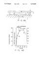
- FIG. 1is a plan view of a single cell of a spatial light modulator constructed in accordance with the present invention, and with the diaphragm removed to show the inner structure of a cell.
- FIG. 2is a cross-sectional view taken along the lines 2--2 of FIG. 1, with the strong back mounting plate removed.
- FIG. 3is a cross-sectional view taken along the lines 3--3 of FIG. 1, as shown with a strong back mounting plate in place.
- FIG. 4Ais a model of a cell without diaphragm flexures of the array of FIGS. 1 through 3 illustrating its operation in response to a deflection voltage.
- FIG. 4Bis a graph depicting the operation of the model of FIG. 4A showing displacement as a function of deflection voltage.
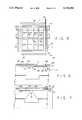
- FIG. 5is a plan view of a cell of an alternative embodiment of a spatial light modulator constructed in accordance with the present invention.
- FIG. 6is a cross-sectional view taken along the lines 6--6 of FIG. 5.
- FIG. 7is a cross-sectional view taken along the lines 7--7 of FIG. 5.
- the spatial light modulator 10 of the present inventionincludes a silicon backplate 11 on which is formed a silicon dioxide coating insulator 12.
- the backplate 11is bonded to and supported on a strong back 13 for supporting the entire device.
- a standoff grid 14 of insulating material such as SiO 2is formed on the backplate 11 to define an array of cells, one of which, 15, is shown in detail. Each cell defines a pixel, which may be square, as shown.
- a deflecting electrode 17is deposited on the oxide coating 12.
- a doped silicon diaphragm 18is bonded to the grid 14 by suitable means such as a bonding interface 19 made of glass.
- Outwardly facing mirror elements 20are deposited on the diaphragm 18, one element 20 on each cell to define a reflective pixel therefor, or the entire outwardly facing mirror surface is coated with the reflecting material.
- the backplate 11is made from a p-type silicon wafer through which vent holes 21 are etched at a center position within each cell 15 from both the upper face and the lower face of backplate 11 creating a through hole.
- a plurality of grooves 22-28are formed on the upper face of the backplate in each cell so as to intersect each other and to intersect the respective vent hole 21.
- Each vent hole 21 and the associated grooves 22-28are constructed of a size to allow gas to escape from within the cell and through the vent hole when the diaphragm element is deflected, and also provides motion damping, which may be set to a critical damping specification, for arresting motion of the diaphragm element after the applied voltage has been changed.
- the diaphragm 18is made of doped silicon so as to be sufficiently conductive to be able to be placed at reference ground potential for operation of the device, a doping level of 10 18 per cm 3 being sufficient for the purpose.
- the movement of the diaphragmis controlled by the electrostatic field developed between it and the cell electrode upon application of the deflection voltage, as will be described.
- the diaphragm 18is etched about the inside border of the grid around each cell 15 to provide a thin wall flexure 30 in the form of a closed curve bounded on the outside by a ridge 32 supported and bonded to the grid 14.
- the flexure 30defines a central diaphragm piston area 37 of greater thickness throughout the inside of the flexure which lies in opposition to the cell electrode 17.
- selective charging of an electrode 17 with an electric signalattracts the diaphragm piston and causes a deflection of the piston toward the electrode and backplate, the displaced air volume being vented throught the vent hole 21. This avoids pressure sensitivity and also mechanically stabilizes the diaphragm motions after a change in applied signal.
- the side of the diaphragm away from the backplateis provided with reflective layer which may be chromium, or other suitable reflecting materials chosen for the wavelength of operation.
- a conductor 33extends from the electrode 17 through the respective vent hole 21 for connection to an electrical sample and hold circuit 36 which may conveniently be connected via a solder bump contact 37 between the strongback 13 and the backplate 11.
- the sample and hold circuit 36is of conventional circuitry, such as used in the monolithic BIFET sample and hold circuit available from National Semiconductor under the designation LF-198 and which is a drivable by an analog logic input XY driver (not shown) having an output from 0 to about 18 volts.
- Layer 38is a silicon integrated circuit containing a suitable circuit 36 for each cell and other circuits (not shown) as necessary for the XY addressable feature.
- Silicon strong back 39is bonded to silicon layer 38 by a bond layer 40.
- Bond layer 40may be a glass layer or other suitable layer to join two silicon surfaces together.
- Silicon backplate 11is etched to form contact pads 41. Bonds 42 of glass or other bonding agents bond contact pads to silicon layer 38. The purpose of the contact pads is to accurately maintain the spacing between backplate 11 and layer 38. It is possible that electrical contact can also be made with this mechanical bond, which if accomplished could replace solder bump 37.
- the materials used in the constructionhave been carefully selected for thermal stability of the assembled device.
- the deviceis micromachined and assembled using generally known silicon forming and bonding technology.
- An example of a procedure for making a spatial light modulator in accordance with the present inventionwill now be given.
- the baseplateis formed from a p-type (boron, 10 16 /cm 3 ) 3 to 6 inch diameter silicon wafer 12 to 25 mils thick.
- the waferis processed to etch the grooves 22-28 and the portion of vent holes 21 etched from the top surface of backplate 11.
- the remainder of vent holes 21are etched from the bottom surface of backplate 11.
- a 4 micron silicon oxide layeris grown to form the standoff grid 14 followed by the field oxide layer 12 of about 5000 angstroms (0.5 microns) for electrical isolation between elements.
- a high temperature platinum-polysilicon (Pt sintered into polycrystaline silicon to form platinum silicide) conductive electrode layeris defined to establish the conductors 33 and each of the electrodes 17.
- a layer of bonding glass 19is selectively laid on the grid 14 for latter use in bonding the diaphragm to the grid.
- the glassis 7059 (Corning) borosilicate glass to match the thermal properties of silicon.
- a simple metalsuch as aluminum can be used in place of the platinum silicide with a lower temperature bonding glass layer such as Corning 7556.
- the diaphragmis manufactured from an p-type (boron, 10 16 /cm 3 ) single crystal silicon wafer, 3-6 inches in diameter, on one side of which is epitaxially grown an n-type (arsenic, or phosphorus, 10 18 /cm 3 ) silicon layer having a thickness of 3 microns, which forms, with the original wafer, a PN junction which is electrically biased to form an etch stop at the junction interface, for use in a later etch process.
- the object of using epitaxial growth techniqueis to allow subsequent removal (by etching) of most of the original wafer and leave only the epitaxially grown layer supported at the peripheral edge by an annular ring of original material.
- the remaining carefully controlled thickness diaphragm elementconsists, then, solely of the epitaxially grown n-type layer, 3 microns thick supported in an annular ring.
- the flexure patternis laid out with suitable photolithography and the flexures 30 etched in the epitaxial layer to a depth of 2 microns leaving a 1 micron flexure strip forming a closed curve which will lie about the inside margin of each cell.
- the diaphragmis then precisely aligned to the backplate and grid.
- a small vacuumis drawn through the vent holes to exert a bonding pressure between the diaphragm and the backplate and the assembly is heated to a bonding temperature of 825° C. (for bonding glass 7059) which is sufficient to fuse the glass coating to the grid and diaphragm and to create a fully bonded structure between the diaphragm and the grid.
- the chromium layeris sputtered onto the entire outward facing surface of the diaphragm through a shadow mask. If needed for specific features i.e. wavelength reflection efficiency, additional metal such as silver or gold can be coated on the chromium layer. If several modulator arrays are made on a single wafer previously etched v grooves can be used as breaking patterns to separate them.
- the relative deflection equation, (2)is appropriate for diaphragm deflected by a pressure difference across the diaphragm where one can relate ⁇ m to the pressure difference as given in equation (3).
- ⁇ mthe pressure difference as given in equation (3).
- qthe pressure difference across the diaphragm
- EYoungs modulus
- hthe diaphragm thickness.
- the completed deviceis an array of identical cells on a single wafer each of which corresponds to that shown in FIGS. 1-3.
- the arraycan be made in various sizes, of which 16 ⁇ 16 and 128 ⁇ 128 arrays being examples.
- 16 ⁇ 16 cellsFor a device with relatively few cells, e.g. 16 ⁇ 16 cells, it is practical to connect each deflecting electrode to an individual wire bond pad around the periphery of the device.
- 128 ⁇ 128 cellsit is not practical to have individual pads.
- the construction appropriate to large arrays shown in FIGS. 1-3calls for the electrodes to pass through the vent holes to a circuit mounted to the backplate, for convenience. In this way XY addressing. techniques reduce the number of leads and use of the vent holes makes for ready access.
- each cell or pixelis padded out independently. This works well for smaller arrays wherein the number of access leads is limited.
- like parts in FIGS. 5-7have been given the same number as those in FIGS. 1-3 raised by 100.
- the electrode 117is padded out through conductor 160, and other conductors 161 (one being shown) are able to continue through the cell and to pass through the opening made at the grid intersections so as to continue unimpeded through the cell array.
- the number of such conductors 161increases as the square of the array area so that this approach is limited.
Landscapes
- Physics & Mathematics (AREA)
- General Physics & Mathematics (AREA)
- Optics & Photonics (AREA)
- Mechanical Light Control Or Optical Switches (AREA)
Abstract
Description
Spatial light modulators are used as an active element in many optical processor applications, such as in correlators and optical neural networks.
The present invention relates to spatial light modulators (SLM) and more particularly to spatial light modulators using deformable mirror technology. More particularly, the present invention relates to an improved spatial light modulator having high diffraction efficiency, low spurious diffraction, excellent thermal stability, and a high power handling capacity.
In one form, spatial light modulators of the deformable mirror type have been made as an array of mirror elements or pixels formed on a membrane or petal structure supported on a grid in spaced relation to a corresponding array of electrodes deposited on a substrate and individually movable by the application of a local electric field as applied to each electrode to deflect the corresponding mirror element. When deflected into an appropriate pattern in accordance with the state of the applied electric signals, the collective deflection of the elements or pixels causes a phase change in the wave front of a light beam reflected from the array so that information carried in the electric signal state is encoded onto a light beam reflected by the array.
Prior art spatial light modulators of this general type are known from U.S. Pat. No. 4,441,791, issued Apr. 10, 1984 to Hornbeck for a Deformable Mirror Light Modulator; U.S. Pat. No. 4,571,603, issued Feb. 18, 1986 to Hornbeck et al for a Deformable Mirror Electrostatic Printer and from publication "Characteristics of the Deformable Mirror Device for Optical Information Processing", Opt. Eng. Nov.-Dec. 1983, vol. 22 No. 6, pg 675-681. In these references there is proposed a spatial light modulator using a polymer diaphragm supported on a grid over an array of electrodes mounted on a backplate. The references describe the theory of operation of such a device. Careful analysis of this type of device reveals that the diffraction efficiency is less than desirable and far less than an appreciable percentage of that available; the temperature sensitivity due to the use of dissimilar material is significant; and the deflection parameters are less than optimum. These limitations are principally due to the use of dissimilar materials; i.e., a polymer diaphragm material on a silicon backplate. The polymer has a very different thermal coefficient of expansion from silicon so that the tension that is developed in the diaphragm changes dramatically over a temperature range. Further, the cavity between the backplate and the diaphragm is pressure sensitive so that the transducer itself becomes pressure sensitive. The drum nature of the deflection of the diaphragm limits the diffraction efficiency. Thus, the devices of the type shown in this art are not readily adaptable for use over a wide temperature range or for modulation purposes involving high frequency operation. Additionally, the use of significant powers of incident radiation beam is also limited due to the thermal limits of the diaphragm, which, for most plastics, would be less than about 200° C.
A number of other prior art patents disclose spatial light modulators of different constructions with, however, similar deficiencies. Such other constructions are exemplified in the following patents: U.S. Pat. No. 4,956,619, issued Sep. 11, 1990 to Hornbeck for a Spatial Light Modulator; EP 0,332,953 A2, issued Mar. 3, 1989 to Hornbeck for a Spatial Light Modulator and Method; U.S. Pat. No. 4,662,746, issued May 5, 1987 to Hornbeck for a Spatial Light Modulator and Method; U.S. Pat. No. 4,615,595, issued Oct. 7, 1986 to Hornbeck for a Frame Addressed Spatial Light Modulator; and U.S. Pat. No. 4,710,732, issued Dec. 1, 1987 to Hornbeck for a Spatial Light Modulator and Method.
Where the structure utilizes a diaphragm formed as a petal or flap structure in which edges of each petal are hinged to a support on one side and otherwise completely free as in U.S. Pat. No. 4,615,595, a problem arises from spurious diffraction even in the absence of intentional deflection of the petals due to the tendency for each of the petals to curl from stresses induced by manufacturing process etching. Also, light modulators using petal constructions have an inherent tilt imparted to the beam which is undesirable.
There is, therefore, a need for an improved compact spatial light modulator which will overcome the limitations and disadvantages of the prior art and which is especially suited for phase modulation of high power laser beams.
In general, it is the object of the present invention to provide an improved spatial light modulator which will overcome the above limitations and disadvantages.
A further object of the invention is to provide a spatial light modulator of the above character which is thermally stable for operating over a wide range of temperatures.
A further object of the invention is to provide a spatial light modulator of the above character which is operable with very high incident power levels as high as 1000 watts.
A further object of the invention is to provide a spatial light modulator of the above character which provides significantly increased diffraction efficiency.
In accordance with the present invention there is provided a spatial light modulator including a silicon backplate having a thin insulating layer on which is deposited a second layer of insulating material forming a standoff grid to define an array of cells. The material on the grid has a similar coefficient of expansion to silicon. An electrode is deposited on said thin insulating layer on said backplate in each cell. A thin membrane of doped silicon is mounted to the standoff grid and over said array of cells and electrodes. A highly reflecting surface is deposited on the membrane on the side facing away from the backplate to create an array of reflective pixels over the array of cells, which when the respective electrode is selectively charged causes the individual portions of the membrane and pixel overlying each cell to be deflected by electrostatic attraction between the membrane and the electrode in accordance with a pattern corresponding to the state of the electrical signals placed on the electrodes. A vent hole is formed in each cell from the electrode side of the backplate to the opposite side thereof for venting gas from the cell when said diaphragm is deflected, and grooves extend across the face of the backplate and over the cell to intersect the vent hole to assist in venting gas out of the cell and through the hole. The vent hole is preferably of a size and constructed for critical damping of the movement of the mass of the deflected diaphragm at said cell to control the movement caused by the electrostatic deflection. Flexures of reduced cross-section are formed in the diaphragm along a closed line extending around the inside perimeter of the stand off grid, so that said diaphragm moves more nearly in piston mode within the flexure.
These and other features of the invention will become apparent from the following description of an improved spatial light modulator structure constructed of essentially a single silicon material throughout, in single crystal form, and to the various features thereof as herein disclosed in the accompanying detailed description and drawings, of which:
FIG. 1 is a plan view of a single cell of a spatial light modulator constructed in accordance with the present invention, and with the diaphragm removed to show the inner structure of a cell.
FIG. 2 is a cross-sectional view taken along thelines 2--2 of FIG. 1, with the strong back mounting plate removed.
FIG. 3 is a cross-sectional view taken along thelines 3--3 of FIG. 1, as shown with a strong back mounting plate in place.
FIG. 4A is a model of a cell without diaphragm flexures of the array of FIGS. 1 through 3 illustrating its operation in response to a deflection voltage.
FIG. 4B is a graph depicting the operation of the model of FIG. 4A showing displacement as a function of deflection voltage.
FIG. 5 is a plan view of a cell of an alternative embodiment of a spatial light modulator constructed in accordance with the present invention.
FIG. 6 is a cross-sectional view taken along the lines 6--6 of FIG. 5.
FIG. 7 is a cross-sectional view taken along thelines 7--7 of FIG. 5.
Thespatial light modulator 10 of the present invention includes a silicon backplate 11 on which is formed a silicondioxide coating insulator 12. The backplate 11 is bonded to and supported on astrong back 13 for supporting the entire device. Astandoff grid 14 of insulating material such as SiO2 is formed on the backplate 11 to define an array of cells, one of which, 15, is shown in detail. Each cell defines a pixel, which may be square, as shown. Within the area of each cell, adeflecting electrode 17 is deposited on theoxide coating 12. A dopedsilicon diaphragm 18 is bonded to thegrid 14 by suitable means such as abonding interface 19 made of glass. Outwardly facingmirror elements 20 are deposited on thediaphragm 18, oneelement 20 on each cell to define a reflective pixel therefor, or the entire outwardly facing mirror surface is coated with the reflecting material.
The backplate 11 is made from a p-type silicon wafer through which vent holes 21 are etched at a center position within eachcell 15 from both the upper face and the lower face of backplate 11 creating a through hole. A plurality of grooves 22-28 are formed on the upper face of the backplate in each cell so as to intersect each other and to intersect therespective vent hole 21. Eachvent hole 21 and the associated grooves 22-28 are constructed of a size to allow gas to escape from within the cell and through the vent hole when the diaphragm element is deflected, and also provides motion damping, which may be set to a critical damping specification, for arresting motion of the diaphragm element after the applied voltage has been changed.
Thediaphragm 18 is made of doped silicon so as to be sufficiently conductive to be able to be placed at reference ground potential for operation of the device, a doping level of 1018 per cm3 being sufficient for the purpose. The movement of the diaphragm is controlled by the electrostatic field developed between it and the cell electrode upon application of the deflection voltage, as will be described.
Thediaphragm 18 is etched about the inside border of the grid around eachcell 15 to provide athin wall flexure 30 in the form of a closed curve bounded on the outside by aridge 32 supported and bonded to thegrid 14. Theflexure 30 defines a centraldiaphragm piston area 37 of greater thickness throughout the inside of the flexure which lies in opposition to thecell electrode 17. In operation, selective charging of anelectrode 17 with an electric signal attracts the diaphragm piston and causes a deflection of the piston toward the electrode and backplate, the displaced air volume being vented throught thevent hole 21. This avoids pressure sensitivity and also mechanically stabilizes the diaphragm motions after a change in applied signal.
The side of the diaphragm away from the backplate is provided with reflective layer which may be chromium, or other suitable reflecting materials chosen for the wavelength of operation.
Aconductor 33 extends from theelectrode 17 through therespective vent hole 21 for connection to an electrical sample and holdcircuit 36 which may conveniently be connected via asolder bump contact 37 between thestrongback 13 and the backplate 11.
The sample and holdcircuit 36 is of conventional circuitry, such as used in the monolithic BIFET sample and hold circuit available from National Semiconductor under the designation LF-198 and which is a drivable by an analog logic input XY driver (not shown) having an output from 0 to about 18 volts.
The upper portion ofstrong back 13 islayer 38.Layer 38 is a silicon integrated circuit containing asuitable circuit 36 for each cell and other circuits (not shown) as necessary for the XY addressable feature.
Siliconstrong back 39 is bonded tosilicon layer 38 by abond layer 40.Bond layer 40 may be a glass layer or other suitable layer to join two silicon surfaces together.
Silicon backplate 11 is etched to formcontact pads 41.Bonds 42 of glass or other bonding agents bond contact pads tosilicon layer 38. The purpose of the contact pads is to accurately maintain the spacing between backplate 11 andlayer 38. It is possible that electrical contact can also be made with this mechanical bond, which if accomplished could replacesolder bump 37.
The materials used in the construction have been carefully selected for thermal stability of the assembled device. The device is micromachined and assembled using generally known silicon forming and bonding technology. An example of a procedure for making a spatial light modulator in accordance with the present invention will now be given.
The baseplate is formed from a p-type (boron, 1016 /cm3) 3 to 6 inchdiameter silicon wafer 12 to 25 mils thick. First, the wafer is processed to etch the grooves 22-28 and the portion of vent holes 21 etched from the top surface of backplate 11. Then the remainder of vent holes 21 are etched from the bottom surface of backplate 11. Then, a 4 micron silicon oxide layer is grown to form thestandoff grid 14 followed by thefield oxide layer 12 of about 5000 angstroms (0.5 microns) for electrical isolation between elements.
Afterwards, a high temperature platinum-polysilicon (Pt sintered into polycrystaline silicon to form platinum silicide) conductive electrode layer is defined to establish theconductors 33 and each of theelectrodes 17. A layer ofbonding glass 19 is selectively laid on thegrid 14 for latter use in bonding the diaphragm to the grid. The glass is 7059 (Corning) borosilicate glass to match the thermal properties of silicon.
Alternatively, a simple metal such as aluminum can be used in place of the platinum silicide with a lower temperature bonding glass layer such as Corning 7556.
The diaphragm is manufactured from an p-type (boron, 1016 /cm3) single crystal silicon wafer, 3-6 inches in diameter, on one side of which is epitaxially grown an n-type (arsenic, or phosphorus, 1018 /cm3) silicon layer having a thickness of 3 microns, which forms, with the original wafer, a PN junction which is electrically biased to form an etch stop at the junction interface, for use in a later etch process. The object of using epitaxial growth technique is to allow subsequent removal (by etching) of most of the original wafer and leave only the epitaxially grown layer supported at the peripheral edge by an annular ring of original material. The remaining carefully controlled thickness diaphragm element consists, then, solely of the epitaxially grown n-type layer, 3 microns thick supported in an annular ring.
The flexure pattern is laid out with suitable photolithography and theflexures 30 etched in the epitaxial layer to a depth of 2 microns leaving a 1 micron flexure strip forming a closed curve which will lie about the inside margin of each cell.
The diaphragm is then precisely aligned to the backplate and grid. A small vacuum is drawn through the vent holes to exert a bonding pressure between the diaphragm and the backplate and the assembly is heated to a bonding temperature of 825° C. (for bonding glass 7059) which is sufficient to fuse the glass coating to the grid and diaphragm and to create a fully bonded structure between the diaphragm and the grid.
The chromium layer is sputtered onto the entire outward facing surface of the diaphragm through a shadow mask. If needed for specific features i.e. wavelength reflection efficiency, additional metal such as silver or gold can be coated on the chromium layer. If several modulator arrays are made on a single wafer previously etched v grooves can be used as breaking patterns to separate them.
Referring now to FIG. 4A and 4B a model of the operation of the cell is shown together with the deflection curves. Using a simplified model then, the incremental attractive force on a circular diaphragm, assumed in FIG. 4A, would be ##EQU1## where d is the distance from electrode to the deflecting diaphragm, r is the radial distance from the axis of symmetry, ω is the diaphragm deflection and V is applied voltage. As an approximation, the relative shape of the diaphragm deflection is assumed to be given by equation (2). The relative deflection equation, (2) is appropriate for diaphragm deflected by a pressure difference across the diaphragm where one can relate ωm to the pressure difference as given in equation (3). In this calculation we assume that the amplitude and shape of the diaphragm deflection is the same when the total pressure force on the diaphragm is equal to the total electrical attractive force exerted on the diaphragm. where q is the pressure difference across the diaphragm, E is Youngs modulus and h is the diaphragm thickness.
One can then integrate the incremental force and obtain the total electrical force on the diaphragm, Fe. ##EQU2##
With this one can calculate ωm as a function of V by substituting Fe divided by the total diaphragm area for q in Equation (2). Thecalculated response curve 50 is shown in solid line FIG. 4B while the measuredcurve 52 is quite close.
The completed device is an array of identical cells on a single wafer each of which corresponds to that shown in FIGS. 1-3. The array can be made in various sizes, of which 16×16 and 128×128 arrays being examples. For a device with relatively few cells, e.g. 16×16 cells, it is practical to connect each deflecting electrode to an individual wire bond pad around the periphery of the device. For a device with many elements, e.g. 128×128 cells, it is not practical to have individual pads. The construction appropriate to large arrays shown in FIGS. 1-3 calls for the electrodes to pass through the vent holes to a circuit mounted to the backplate, for convenience. In this way XY addressing. techniques reduce the number of leads and use of the vent holes makes for ready access.
Referring to FIGS. 5-7, an alternative form of the invention is shown in which each cell or pixel is padded out independently. This works well for smaller arrays wherein the number of access leads is limited. In order to minimize repetition, like parts in FIGS. 5-7 have been given the same number as those in FIGS. 1-3 raised by 100. As shown, theelectrode 117 is padded out throughconductor 160, and other conductors 161 (one being shown) are able to continue through the cell and to pass through the opening made at the grid intersections so as to continue unimpeded through the cell array. As is evident, the number ofsuch conductors 161 increases as the square of the array area so that this approach is limited.
Dimensions and features for a typical 128×128 array include the following:
overall active area: 10 cm×10 cm (made from 6 inch silicon wafers.)
backplate: silicon p-type (boron) 0.5 mm thick
grid: 4 micron SiO2 ×50 micron
field oxide layer: 5000 Å SiO2
strongback: silicon layer with XY addressable circuits bonded to a thick piece, ˜1 cm thick, of silicon or 7740 glass.
diaphragm thickness after processing: 3 microns
flexure thickness: 1 micron
unit cell: 0.8 mm×0.8 mm
pixel reflectivity>0.98
pixel deflection: 0 to 1 micron
area fill factor>0.6
pixel frequency response: DC to 20 kHz
electrode operating range: 0 to 17 volts
diaphragm sensitivity: δ=0.5 micron/12 volts
stress for δ=0.5 micron: 17 MPa.
Claims (17)
1. A spatial light modulator comprising:
a silicon backplate having an insulating layer therein,
a standoff grid of insulating material deposited on said backplate to define an array of cells covering an area thereof and forming a second layer thereon,
a plurality of electrodes, each electrode being deposited in one of said cells and on said backplate,
a membrane of doped silicon mounted to said standoff grid and over said array of cells and electrodes,
means forming a mirror surface on said membrane on the side facing away from said backplate.
2. The spatial light modulator as in claim 1 further including:
means for selectively charging and discharging each electrode,
whereby each charged electrode causes the individual portions of said membrane overlying each corresponding cell to be deflected by electrostatic attraction between the membrane and the electrode in accordance with a pattern corresponding to the state of the electrical signals placed on said electrodes.
3. The spatial light modulator as in claim 1 further including:
means forming a vent hole in each cell from the electrode side of the backplate to the opposite side thereof for venting gas from said cell when said membrane is deflected.
4. The spatial light modulator as in claim 3 further including:
groove means extending across the face of said backplate and over said cell to intersect said vent hole to assist in venting gas out of said cell and through said hole.
5. The spatial light modulator as in claim 3 wherein said vent hole is of a size and constructed for critical damping of the movement of the mass of said membrane at said cell.
6. The spatial light modulator as in claim 4 wherein said vent hole and said groove are collectively of a size for providing critical damping of the movement of the mass of said membrane.
7. The spatial light modulator as in claim 1 further including:
a plurality of electrical conductors connected to each of said electrodes respectively.
8. The spatial light modulator as in claim 4 further including:
a plurality of electrical conductors connected to each of said electrodes, respectively, through the respective vent hole for each element.
9. The spatial light modulator as in claim 1 wherein said membrane comprises:
a doped thin coating of silicon epitaxially grown on a silicon wafer from which substantially the entire original wafer has been etched away.
10. The spatial light modulator as in claim 1 further in which:
said electrodes are made of platinum silicide.
11. The spatial light modulator as in claim 1 further in which:
said electrodes are made of a layer of an elemental metal or layers of elemental metals.
12. The spatial light modulator as in claim 1 further in which:
said stand off grid is made of silicon dioxide (SiO2) deposited on said silicon backplate.
13. The spatial light modulator as in claim 1 wherein:
said membrane is made about 3 microns in thickness, and
said stand off grid is made about 4 microns in height.
14. The spatial light modulator as in claim 1 further in which:
said backplate and said membrane are made of single crystal silicon material.
15. The spatial light modulator as in claim 1 further including:
a thin oxide layer covering said electrode to prevent sticking of said membrane to said electrode.
16. The spatial light modulator as in claim 1 further in which:
said membrane is provided with means forming flexures of reduced cross-section formed therein along a closed line extending around the inside perimeter of said stand off grid, so that said membrane moves more nearly in piston mode within said flexure means.
17. A spatial light modulator comprising:
a backplate made of doped single crystal high temperature material,
a diaphragm made of doped single crystal material having the same coefficient of thermal expansion as said material of said backplate,
a standoff grid formed on one side of said backplate,
said grid including a plurality of raised ridges formed to project up from one side of the backplate for defining the periphery of a plurality of area elements and for spacing said diaphragm from the backplate,
means bonding said diaphragm on said grid,
a plurality of electrodes disposed on said backplate and within each of said plurality of area elements respectively,
said diaphragm having a thickness small enough to be readily flexed by electrostatic forces applied between said electrodes and said diaphragm,
means in said diaphragm for forming flexures therein around the inside of each said area periphery so that, when flexed, the region of said diaphragm within the flexures preferentially moves in piston mode,
means forming a plurality of vent holes in said backplate with at least one vent hole for each area element, each of said vent holes having a size for critically damping the movement of said diaphragm as caused by said electrode,
electrical connector means for connecting to each of said electrodes through respective vent hole to the opposite side of said backplate.
Priority Applications (5)
| Application Number | Priority Date | Filing Date | Title |
|---|---|---|---|
| US07/735,392US5170283A (en) | 1991-07-24 | 1991-07-24 | Silicon spatial light modulator |
| GB9215419AGB2258055B (en) | 1991-07-24 | 1992-07-21 | Silicon spatial light modulator |
| DE4224349ADE4224349A1 (en) | 1991-07-24 | 1992-07-23 | ROOM LIGHT MODULATOR MADE OF SILICON |
| FR9209101AFR2679665B1 (en) | 1991-07-24 | 1992-07-23 | LIGHT SPACE MODULATOR. |
| JP4198602AJPH05257070A (en) | 1991-07-24 | 1992-07-24 | Silicon spatial light modulator |
Applications Claiming Priority (1)
| Application Number | Priority Date | Filing Date | Title |
|---|---|---|---|
| US07/735,392US5170283A (en) | 1991-07-24 | 1991-07-24 | Silicon spatial light modulator |
Publications (1)
| Publication Number | Publication Date |
|---|---|
| US5170283Atrue US5170283A (en) | 1992-12-08 |
Family
ID=24955591
Family Applications (1)
| Application Number | Title | Priority Date | Filing Date |
|---|---|---|---|
| US07/735,392Expired - LifetimeUS5170283A (en) | 1991-07-24 | 1991-07-24 | Silicon spatial light modulator |
Country Status (5)
| Country | Link |
|---|---|
| US (1) | US5170283A (en) |
| JP (1) | JPH05257070A (en) |
| DE (1) | DE4224349A1 (en) |
| FR (1) | FR2679665B1 (en) |
| GB (1) | GB2258055B (en) |
Cited By (154)
| Publication number | Priority date | Publication date | Assignee | Title |
|---|---|---|---|---|
| US5223971A (en)* | 1991-12-31 | 1993-06-29 | Texas Instruments Incorporated | Light beam steering with deformable membrane device |
| US5408253A (en)* | 1992-08-03 | 1995-04-18 | Eastman Kodak Company | Integrated galvanometer scanning device |
| US5452138A (en)* | 1991-07-31 | 1995-09-19 | Texas Instruments Incorporated | Deformable mirror device with integral color filter |
| US5585956A (en)* | 1993-07-31 | 1996-12-17 | Daewoo Electronics Co, Ltd. | Electrostrictive actuated mirror array |
| US5808797A (en) | 1992-04-28 | 1998-09-15 | Silicon Light Machines | Method and apparatus for modulating a light beam |
| US5818563A (en)* | 1996-07-23 | 1998-10-06 | Ibm Corporation | Substrate structure and assembly method for reduced spatial light modulator size |
| US5841579A (en) | 1995-06-07 | 1998-11-24 | Silicon Light Machines | Flat diffraction grating light valve |
| US5844711A (en)* | 1997-01-10 | 1998-12-01 | Northrop Grumman Corporation | Tunable spatial light modulator |
| US5883614A (en)* | 1995-09-13 | 1999-03-16 | Samsung Electronics Co., Ltd. | Reflection type display utilizing charge coupled devices |
| US5982553A (en) | 1997-03-20 | 1999-11-09 | Silicon Light Machines | Display device incorporating one-dimensional grating light-valve array |
| US6088102A (en) | 1997-10-31 | 2000-07-11 | Silicon Light Machines | Display apparatus including grating light-valve array and interferometric optical system |
| US6101036A (en) | 1998-06-23 | 2000-08-08 | Silicon Light Machines | Embossed diffraction grating alone and in combination with changeable image display |
| US6115326A (en)* | 1998-10-22 | 2000-09-05 | Integrated Medical Systems, Inc. | Ultrasonic micro-machined selectable transducer array |
| US6130770A (en) | 1998-06-23 | 2000-10-10 | Silicon Light Machines | Electron gun activated grating light valve |
| US6215579B1 (en) | 1998-06-24 | 2001-04-10 | Silicon Light Machines | Method and apparatus for modulating an incident light beam for forming a two-dimensional image |
| US6271808B1 (en) | 1998-06-05 | 2001-08-07 | Silicon Light Machines | Stereo head mounted display using a single display device |
| US6307663B1 (en) | 2000-01-26 | 2001-10-23 | Eastman Kodak Company | Spatial light modulator with conformal grating device |
| US6411425B1 (en) | 2000-09-27 | 2002-06-25 | Eastman Kodak Company | Electromechanical grating display system with spatially separated light beams |
| US6476848B2 (en) | 2000-12-21 | 2002-11-05 | Eastman Kodak Company | Electromechanical grating display system with segmented waveplate |
| WO2002063596A3 (en)* | 2001-02-07 | 2002-11-07 | Movaz Networks Inc | Multiplexed analog control system for electrostatic actuator array |
| KR100368366B1 (en)* | 1994-03-07 | 2003-03-28 | 텍사스 인스트루먼츠 인코포레이티드 | Control Method of Digital Micromirror Device |
| US6608711B2 (en)* | 2000-03-03 | 2003-08-19 | Axsun Technologies, Inc. | Silicon on insulator optical membrane structure for fabry-perot MOEMS filter |
| US6622368B1 (en)* | 1998-06-11 | 2003-09-23 | Sonionmems A/S | Method of manufacturing a transducer having a diaphragm with a predetermined tension |
| US20040027565A1 (en)* | 2001-04-06 | 2004-02-12 | Nico Correns | Pressure compensating device for optical apparatus |
| US6707591B2 (en) | 2001-04-10 | 2004-03-16 | Silicon Light Machines | Angled illumination for a single order light modulator based projection system |
| US6712480B1 (en) | 2002-09-27 | 2004-03-30 | Silicon Light Machines | Controlled curvature of stressed micro-structures |
| US6714337B1 (en) | 2002-06-28 | 2004-03-30 | Silicon Light Machines | Method and device for modulating a light beam and having an improved gamma response |
| US6728023B1 (en) | 2002-05-28 | 2004-04-27 | Silicon Light Machines | Optical device arrays with optimized image resolution |
| US6747781B2 (en) | 2001-06-25 | 2004-06-08 | Silicon Light Machines, Inc. | Method, apparatus, and diffuser for reducing laser speckle |
| US20040113514A1 (en)* | 2002-12-12 | 2004-06-17 | North Howard L. | Method for electronic damping of electrostatic positioners |
| US6764875B2 (en) | 1998-07-29 | 2004-07-20 | Silicon Light Machines | Method of and apparatus for sealing an hermetic lid to a semiconductor die |
| US6767751B2 (en) | 2002-05-28 | 2004-07-27 | Silicon Light Machines, Inc. | Integrated driver process flow |
| US6782205B2 (en) | 2001-06-25 | 2004-08-24 | Silicon Light Machines | Method and apparatus for dynamic equalization in wavelength division multiplexing |
| US6800238B1 (en) | 2002-01-15 | 2004-10-05 | Silicon Light Machines, Inc. | Method for domain patterning in low coercive field ferroelectrics |
| US6801354B1 (en) | 2002-08-20 | 2004-10-05 | Silicon Light Machines, Inc. | 2-D diffraction grating for substantially eliminating polarization dependent losses |
| US6806997B1 (en) | 2003-02-28 | 2004-10-19 | Silicon Light Machines, Inc. | Patterned diffractive light modulator ribbon for PDL reduction |
| US6813059B2 (en) | 2002-06-28 | 2004-11-02 | Silicon Light Machines, Inc. | Reduced formation of asperities in contact micro-structures |
| US6822797B1 (en) | 2002-05-31 | 2004-11-23 | Silicon Light Machines, Inc. | Light modulator structure for producing high-contrast operation using zero-order light |
| KR100459409B1 (en)* | 2002-10-24 | 2004-12-03 | 엘지전자 주식회사 | Spatial light modulator and manufacturing method thereof |
| KR100459408B1 (en)* | 2002-10-24 | 2004-12-03 | 엘지전자 주식회사 | Spatial light modulator and manufacturing method thereof |
| KR100459410B1 (en)* | 2002-10-31 | 2004-12-03 | 엘지전자 주식회사 | Light modulator and method for producing of light modulator |
| US6829077B1 (en) | 2003-02-28 | 2004-12-07 | Silicon Light Machines, Inc. | Diffractive light modulator with dynamically rotatable diffraction plane |
| US6829258B1 (en) | 2002-06-26 | 2004-12-07 | Silicon Light Machines, Inc. | Rapidly tunable external cavity laser |
| US6829092B2 (en) | 2001-08-15 | 2004-12-07 | Silicon Light Machines, Inc. | Blazed grating light valve |
| EP1351087A3 (en)* | 2002-03-18 | 2005-01-05 | Bookham Technology PLC | Micro-mirrors with variable focal length, and optical components comprising micro-mirrors |
| US6865346B1 (en) | 2001-06-05 | 2005-03-08 | Silicon Light Machines Corporation | Fiber optic transceiver |
| US6872984B1 (en) | 1998-07-29 | 2005-03-29 | Silicon Light Machines Corporation | Method of sealing a hermetic lid to a semiconductor die at an angle |
| US6908201B2 (en) | 2002-06-28 | 2005-06-21 | Silicon Light Machines Corporation | Micro-support structures |
| US6922272B1 (en) | 2003-02-14 | 2005-07-26 | Silicon Light Machines Corporation | Method and apparatus for leveling thermal stress variations in multi-layer MEMS devices |
| US6922273B1 (en) | 2003-02-28 | 2005-07-26 | Silicon Light Machines Corporation | PDL mitigation structure for diffractive MEMS and gratings |
| US6927891B1 (en) | 2002-12-23 | 2005-08-09 | Silicon Light Machines Corporation | Tilt-able grating plane for improved crosstalk in 1×N blaze switches |
| US6928207B1 (en) | 2002-12-12 | 2005-08-09 | Silicon Light Machines Corporation | Apparatus for selectively blocking WDM channels |
| US6934070B1 (en) | 2002-12-18 | 2005-08-23 | Silicon Light Machines Corporation | Chirped optical MEM device |
| US6947613B1 (en) | 2003-02-11 | 2005-09-20 | Silicon Light Machines Corporation | Wavelength selective switch and equalizer |
| US6956995B1 (en) | 2001-11-09 | 2005-10-18 | Silicon Light Machines Corporation | Optical communication arrangement |
| US6956878B1 (en) | 2000-02-07 | 2005-10-18 | Silicon Light Machines Corporation | Method and apparatus for reducing laser speckle using polarization averaging |
| US6987600B1 (en) | 2002-12-17 | 2006-01-17 | Silicon Light Machines Corporation | Arbitrary phase profile for better equalization in dynamic gain equalizer |
| US6991953B1 (en) | 2001-09-13 | 2006-01-31 | Silicon Light Machines Corporation | Microelectronic mechanical system and methods |
| EP1635208A1 (en)* | 2004-09-10 | 2006-03-15 | Olympus Corporation | Deformable mirror |
| US20060056004A1 (en)* | 2004-09-14 | 2006-03-16 | Adel Jilani | Flexure |
| US7027202B1 (en) | 2003-02-28 | 2006-04-11 | Silicon Light Machines Corp | Silicon substrate as a light modulator sacrificial layer |
| US7042611B1 (en) | 2003-03-03 | 2006-05-09 | Silicon Light Machines Corporation | Pre-deflected bias ribbons |
| US7054515B1 (en) | 2002-05-30 | 2006-05-30 | Silicon Light Machines Corporation | Diffractive light modulator-based dynamic equalizer with integrated spectral monitor |
| EP1662290A1 (en)* | 2004-11-30 | 2006-05-31 | Northrop Grumman Corporation | Bi-directionally actuated thin membrane mirror |
| US7057795B2 (en) | 2002-08-20 | 2006-06-06 | Silicon Light Machines Corporation | Micro-structures with individually addressable ribbon pairs |
| US7057819B1 (en) | 2002-12-17 | 2006-06-06 | Silicon Light Machines Corporation | High contrast tilting ribbon blazed grating |
| US7068372B1 (en) | 2003-01-28 | 2006-06-27 | Silicon Light Machines Corporation | MEMS interferometer-based reconfigurable optical add-and-drop multiplexor |
| US20060148121A1 (en)* | 2005-01-03 | 2006-07-06 | Miradia Inc. | Method and structure for forming an integrated spatial light modulator |
| US20060262126A1 (en)* | 1999-10-05 | 2006-11-23 | Idc, Llc A Delaware Limited Liability Company | Transparent thin films |
| US20060261330A1 (en)* | 1994-05-05 | 2006-11-23 | Miles Mark W | MEMS device and method of forming a MEMS device |
| US7177081B2 (en) | 2001-03-08 | 2007-02-13 | Silicon Light Machines Corporation | High contrast grating light valve type device |
| US7286764B1 (en) | 2003-02-03 | 2007-10-23 | Silicon Light Machines Corporation | Reconfigurable modulator-based optical add-and-drop multiplexer |
| CN100362387C (en)* | 2005-11-18 | 2008-01-16 | 重庆大学 | Electrostatic Charpy Interferometric Light Modulator |
| US20080036795A1 (en)* | 1994-05-05 | 2008-02-14 | Idc, Llc | Method and device for modulating light |
| US20080037093A1 (en)* | 1994-05-05 | 2008-02-14 | Idc, Llc | Method and device for multi-color interferometric modulation |
| US20080088910A1 (en)* | 1994-05-05 | 2008-04-17 | Idc, Llc | System and method for a mems device |
| US20080088908A1 (en)* | 1994-05-05 | 2008-04-17 | Idc, Llc | System and method for a mems device |
| US20080088904A1 (en)* | 1993-03-17 | 2008-04-17 | Idc, Llc | Method and device for modulating light with semiconductor substrate |
| US20080088911A1 (en)* | 1994-05-05 | 2008-04-17 | Idc, Llc | System and method for a mems device |
| US20080088912A1 (en)* | 1994-05-05 | 2008-04-17 | Idc, Llc | System and method for a mems device |
| US20080112035A1 (en)* | 2004-09-27 | 2008-05-15 | Idc, Llc | Methods and devices for inhibiting tilting of a movable element in a mems device |
| US20080121503A1 (en)* | 2006-11-02 | 2008-05-29 | Sampsell Jeffrey B | Compatible MEMS switch architecture |
| US20080130089A1 (en)* | 1994-05-05 | 2008-06-05 | Idc, Llc | METHOD OF FABRICATING MEMS DEVICES (SUCH AS IMod) COMPRISING USING A GAS PHASE ETCHANT TO REMOVE A LAYER |
| US7391973B1 (en) | 2003-02-28 | 2008-06-24 | Silicon Light Machines Corporation | Two-stage gain equalizer |
| US20080247028A1 (en)* | 2004-09-27 | 2008-10-09 | Idc, Llc | Method and device for multistate interferometric light modulation |
| US20090068781A1 (en)* | 2004-05-04 | 2009-03-12 | Idc, Llc | Method of manufacture for microelectromechanical devices |
| US20090071932A1 (en)* | 2007-09-14 | 2009-03-19 | Qualcomm Mems Technologies, Inc. | Etching processes used in mems production |
| US20090080060A1 (en)* | 1996-12-19 | 2009-03-26 | Idc, Llc | Separable modulator |
| US20090135463A1 (en)* | 1998-04-08 | 2009-05-28 | Idc, Llc | Moveable micro-electromechanical device |
| US7630119B2 (en) | 2004-09-27 | 2009-12-08 | Qualcomm Mems Technologies, Inc. | Apparatus and method for reducing slippage between structures in an interferometric modulator |
| US7629197B2 (en) | 2006-10-18 | 2009-12-08 | Qualcomm Mems Technologies, Inc. | Spatial light modulator |
| US7630121B2 (en) | 2007-07-02 | 2009-12-08 | Qualcomm Mems Technologies, Inc. | Electromechanical device with optical function separated from mechanical and electrical function |
| US20090323166A1 (en)* | 2008-06-25 | 2009-12-31 | Qualcomm Mems Technologies, Inc. | Backlight displays |
| US7643202B2 (en) | 2007-05-09 | 2010-01-05 | Qualcomm Mems Technologies, Inc. | Microelectromechanical system having a dielectric movable membrane and a mirror |
| US7649671B2 (en) | 2006-06-01 | 2010-01-19 | Qualcomm Mems Technologies, Inc. | Analog interferometric modulator device with electrostatic actuation and release |
| WO2009089946A3 (en)* | 2008-01-16 | 2010-01-21 | Robert Bosch Gmbh | Micromechanical component and method for producing a micromechanical component |
| US20100039370A1 (en)* | 1996-12-19 | 2010-02-18 | Idc, Llc | Method of making a light modulating display device and associated transistor circuitry and structures thereof |
| US20100039696A1 (en)* | 2008-08-12 | 2010-02-18 | Qualcomm Mems Technologies, Inc. | Method and apparatus to reduce or eliminate stiction and image retention in interferometric modulator devices |
| WO2009154981A3 (en)* | 2008-05-27 | 2010-03-11 | Tufts University | Mems microphone array on a chip |
| US20100109102A1 (en)* | 2005-01-03 | 2010-05-06 | Miradia Inc. | Method and structure for forming a gyroscope and accelerometer |
| US7715085B2 (en) | 2007-05-09 | 2010-05-11 | Qualcomm Mems Technologies, Inc. | Electromechanical system having a dielectric movable membrane and a mirror |
| US7715079B2 (en) | 2007-12-07 | 2010-05-11 | Qualcomm Mems Technologies, Inc. | MEMS devices requiring no mechanical support |
| US7742220B2 (en) | 2007-03-28 | 2010-06-22 | Qualcomm Mems Technologies, Inc. | Microelectromechanical device and method utilizing conducting layers separated by stops |
| US7746539B2 (en) | 2008-06-25 | 2010-06-29 | Qualcomm Mems Technologies, Inc. | Method for packing a display device and the device obtained thereof |
| US7773286B2 (en) | 2007-09-14 | 2010-08-10 | Qualcomm Mems Technologies, Inc. | Periodic dimple array |
| US7782517B2 (en) | 2007-06-21 | 2010-08-24 | Qualcomm Mems Technologies, Inc. | Infrared and dual mode displays |
| US7787173B2 (en) | 2004-09-27 | 2010-08-31 | Qualcomm Mems Technologies, Inc. | System and method for multi-level brightness in interferometric modulation |
| US20100245980A1 (en)* | 1996-11-05 | 2010-09-30 | Qualcomm Mems Technologies, Inc. | System and method for a mems device |
| US7808694B2 (en) | 1994-05-05 | 2010-10-05 | Qualcomm Mems Technologies, Inc. | Method and device for modulating light |
| US7835061B2 (en) | 2006-06-28 | 2010-11-16 | Qualcomm Mems Technologies, Inc. | Support structures for free-standing electromechanical devices |
| US7847999B2 (en) | 2007-09-14 | 2010-12-07 | Qualcomm Mems Technologies, Inc. | Interferometric modulator display devices |
| US20100315695A1 (en)* | 1995-05-01 | 2010-12-16 | Miles Mark W | Microelectromechanical device with restoring electrode |
| US7859740B2 (en) | 2008-07-11 | 2010-12-28 | Qualcomm Mems Technologies, Inc. | Stiction mitigation with integrated mech micro-cantilevers through vertical stress gradient control |
| US7884989B2 (en) | 2005-05-27 | 2011-02-08 | Qualcomm Mems Technologies, Inc. | White interferometric modulators and methods for forming the same |
| US7889415B2 (en) | 2004-09-27 | 2011-02-15 | Qualcomm Mems Technologies, Inc. | Device having a conductive light absorbing mask and method for fabricating same |
| US7898723B2 (en) | 2008-04-02 | 2011-03-01 | Qualcomm Mems Technologies, Inc. | Microelectromechanical systems display element with photovoltaic structure |
| US7936497B2 (en) | 2004-09-27 | 2011-05-03 | Qualcomm Mems Technologies, Inc. | MEMS device having deformable membrane characterized by mechanical persistence |
| US7944604B2 (en) | 2008-03-07 | 2011-05-17 | Qualcomm Mems Technologies, Inc. | Interferometric modulator in transmission mode |
| US7944599B2 (en) | 2004-09-27 | 2011-05-17 | Qualcomm Mems Technologies, Inc. | Electromechanical device with optical function separated from mechanical and electrical function |
| US7952787B2 (en) | 2006-06-30 | 2011-05-31 | Qualcomm Mems Technologies, Inc. | Method of manufacturing MEMS devices providing air gap control |
| US7969638B2 (en) | 2008-04-10 | 2011-06-28 | Qualcomm Mems Technologies, Inc. | Device having thin black mask and method of fabricating the same |
| US7982700B2 (en) | 2004-09-27 | 2011-07-19 | Qualcomm Mems Technologies, Inc. | Conductive bus structure for interferometric modulator array |
| US7999993B2 (en) | 2004-09-27 | 2011-08-16 | Qualcomm Mems Technologies, Inc. | Reflective display device having viewable display on both sides |
| US8008736B2 (en) | 2004-09-27 | 2011-08-30 | Qualcomm Mems Technologies, Inc. | Analog interferometric modulator device |
| US8014059B2 (en) | 1994-05-05 | 2011-09-06 | Qualcomm Mems Technologies, Inc. | System and method for charge control in a MEMS device |
| US8023167B2 (en) | 2008-06-25 | 2011-09-20 | Qualcomm Mems Technologies, Inc. | Backlight displays |
| US8054527B2 (en) | 2007-10-23 | 2011-11-08 | Qualcomm Mems Technologies, Inc. | Adjustably transmissive MEMS-based devices |
| US8058549B2 (en) | 2007-10-19 | 2011-11-15 | Qualcomm Mems Technologies, Inc. | Photovoltaic devices with integrated color interferometric film stacks |
| US8068269B2 (en) | 2008-03-27 | 2011-11-29 | Qualcomm Mems Technologies, Inc. | Microelectromechanical device with spacing layer |
| US8081370B2 (en) | 2004-09-27 | 2011-12-20 | Qualcomm Mems Technologies, Inc. | Support structures for electromechanical systems and methods of fabricating the same |
| US8081373B2 (en) | 2007-07-31 | 2011-12-20 | Qualcomm Mems Technologies, Inc. | Devices and methods for enhancing color shift of interferometric modulators |
| US8115987B2 (en) | 2007-02-01 | 2012-02-14 | Qualcomm Mems Technologies, Inc. | Modulating the intensity of light from an interferometric reflector |
| US8164821B2 (en) | 2008-02-22 | 2012-04-24 | Qualcomm Mems Technologies, Inc. | Microelectromechanical device with thermal expansion balancing layer or stiffening layer |
| US8270062B2 (en) | 2009-09-17 | 2012-09-18 | Qualcomm Mems Technologies, Inc. | Display device with at least one movable stop element |
| US8270056B2 (en) | 2009-03-23 | 2012-09-18 | Qualcomm Mems Technologies, Inc. | Display device with openings between sub-pixels and method of making same |
| US20120268805A1 (en)* | 2010-01-04 | 2012-10-25 | Shanghai Lexvu Opto Microelectonics Technology Co., Ltd. | Tri wavelength diffraction modulator and a method for modulation |
| US8358266B2 (en) | 2008-09-02 | 2013-01-22 | Qualcomm Mems Technologies, Inc. | Light turning device with prismatic light turning features |
| US8405899B2 (en) | 2004-09-27 | 2013-03-26 | Qualcomm Mems Technologies, Inc | Photonic MEMS and structures |
| US8488228B2 (en) | 2009-09-28 | 2013-07-16 | Qualcomm Mems Technologies, Inc. | Interferometric display with interferometric reflector |
| US8536059B2 (en) | 2007-02-20 | 2013-09-17 | Qualcomm Mems Technologies, Inc. | Equipment and methods for etching of MEMS |
| US8659816B2 (en) | 2011-04-25 | 2014-02-25 | Qualcomm Mems Technologies, Inc. | Mechanical layer and methods of making the same |
| US8736939B2 (en) | 2011-11-04 | 2014-05-27 | Qualcomm Mems Technologies, Inc. | Matching layer thin-films for an electromechanical systems reflective display device |
| US8797628B2 (en) | 2007-10-19 | 2014-08-05 | Qualcomm Memstechnologies, Inc. | Display with integrated photovoltaic device |
| US8797632B2 (en) | 2010-08-17 | 2014-08-05 | Qualcomm Mems Technologies, Inc. | Actuation and calibration of charge neutral electrode of a display device |
| US8817357B2 (en) | 2010-04-09 | 2014-08-26 | Qualcomm Mems Technologies, Inc. | Mechanical layer and methods of forming the same |
| US8885244B2 (en) | 2004-09-27 | 2014-11-11 | Qualcomm Mems Technologies, Inc. | Display device |
| US8928967B2 (en) | 1998-04-08 | 2015-01-06 | Qualcomm Mems Technologies, Inc. | Method and device for modulating light |
| US8941631B2 (en) | 2007-11-16 | 2015-01-27 | Qualcomm Mems Technologies, Inc. | Simultaneous light collection and illumination on an active display |
| US8963159B2 (en) | 2011-04-04 | 2015-02-24 | Qualcomm Mems Technologies, Inc. | Pixel via and methods of forming the same |
| US8971675B2 (en) | 2006-01-13 | 2015-03-03 | Qualcomm Mems Technologies, Inc. | Interconnect structure for MEMS device |
| US8979349B2 (en) | 2009-05-29 | 2015-03-17 | Qualcomm Mems Technologies, Inc. | Illumination devices and methods of fabrication thereof |
| US9057872B2 (en) | 2010-08-31 | 2015-06-16 | Qualcomm Mems Technologies, Inc. | Dielectric enhanced mirror for IMOD display |
| US9134527B2 (en) | 2011-04-04 | 2015-09-15 | Qualcomm Mems Technologies, Inc. | Pixel via and methods of forming the same |
| US11650422B2 (en) | 2017-10-23 | 2023-05-16 | Vuzix Corporation | Active correction of aberrations in optical systems |
Families Citing this family (6)
| Publication number | Priority date | Publication date | Assignee | Title |
|---|---|---|---|---|
| KR100213281B1 (en)* | 1994-10-31 | 1999-08-02 | 전주범 | Light Path Control |
| KR960018646A (en)* | 1994-11-14 | 1996-06-17 | 배순훈 | Manufacturing method of optical path control device |
| KR100203577B1 (en)* | 1994-12-19 | 1999-06-15 | 배순훈 | Optical projection system and its fabrication system |
| JP2008152016A (en)* | 2006-12-18 | 2008-07-03 | Toshiba Corp | Deformable mirror device and fundus observation device |
| JP2009042458A (en)* | 2007-08-08 | 2009-02-26 | Toshiba Corp | Deformable mirror apparatus and fundus observation apparatus using the deformable mirror apparatus |
| US9630837B1 (en)* | 2016-01-15 | 2017-04-25 | Taiwan Semiconductor Manufacturing Company Ltd. | MEMS structure and manufacturing method thereof |
Citations (17)
| Publication number | Priority date | Publication date | Assignee | Title |
|---|---|---|---|---|
| US3001447A (en)* | 1957-08-29 | 1961-09-26 | Zeiss Ikon A G Stuttgart | Image reproducing device for visible and invisible radiation images |
| US3463572A (en)* | 1966-10-21 | 1969-08-26 | Perkin Elmer Corp | Optical phase modulation apparatus |
| US3746785A (en)* | 1971-11-26 | 1973-07-17 | Bendix Corp | Deflectable membrane optical modulator |
| US3796480A (en)* | 1968-12-26 | 1974-03-12 | Perkin Elmer Corp | Membrane light modulator |
| US4087810A (en)* | 1976-06-30 | 1978-05-02 | International Business Machines Corporation | Membrane deformographic display, and method of making |
| US4229732A (en)* | 1978-12-11 | 1980-10-21 | International Business Machines Corporation | Micromechanical display logic and array |
| US4248504A (en)* | 1978-12-08 | 1981-02-03 | Itek Corporation | Piezoelectric wavefront modulator |
| US4441791A (en)* | 1980-09-02 | 1984-04-10 | Texas Instruments Incorporated | Deformable mirror light modulator |
| US4566935A (en)* | 1984-07-31 | 1986-01-28 | Texas Instruments Incorporated | Spatial light modulator and method |
| US4571603A (en)* | 1981-11-03 | 1986-02-18 | Texas Instruments Incorporated | Deformable mirror electrostatic printer |
| US4615595A (en)* | 1984-10-10 | 1986-10-07 | Texas Instruments Incorporated | Frame addressed spatial light modulator |
| US4662746A (en)* | 1985-10-30 | 1987-05-05 | Texas Instruments Incorporated | Spatial light modulator and method |
| US4710732A (en)* | 1984-07-31 | 1987-12-01 | Texas Instruments Incorporated | Spatial light modulator and method |
| EP0332953A2 (en)* | 1988-03-16 | 1989-09-20 | Texas Instruments Incorporated | Spatial light modulator and method |
| US4954789A (en)* | 1989-09-28 | 1990-09-04 | Texas Instruments Incorporated | Spatial light modulator |
| US4956619A (en)* | 1988-02-19 | 1990-09-11 | Texas Instruments Incorporated | Spatial light modulator |
| US5061049A (en)* | 1984-08-31 | 1991-10-29 | Texas Instruments Incorporated | Spatial light modulator and method |
Family Cites Families (1)
| Publication number | Priority date | Publication date | Assignee | Title |
|---|---|---|---|---|
| ATE50864T1 (en)* | 1985-10-16 | 1990-03-15 | British Telecomm | FABRY-PEROT INTERFEROMETER. |
- 1991
- 1991-07-24USUS07/735,392patent/US5170283A/ennot_activeExpired - Lifetime
- 1992
- 1992-07-21GBGB9215419Apatent/GB2258055B/ennot_activeExpired - Fee Related
- 1992-07-23FRFR9209101Apatent/FR2679665B1/ennot_activeExpired - Fee Related
- 1992-07-23DEDE4224349Apatent/DE4224349A1/ennot_activeWithdrawn
- 1992-07-24JPJP4198602Apatent/JPH05257070A/enactivePending
Patent Citations (17)
| Publication number | Priority date | Publication date | Assignee | Title |
|---|---|---|---|---|
| US3001447A (en)* | 1957-08-29 | 1961-09-26 | Zeiss Ikon A G Stuttgart | Image reproducing device for visible and invisible radiation images |
| US3463572A (en)* | 1966-10-21 | 1969-08-26 | Perkin Elmer Corp | Optical phase modulation apparatus |
| US3796480A (en)* | 1968-12-26 | 1974-03-12 | Perkin Elmer Corp | Membrane light modulator |
| US3746785A (en)* | 1971-11-26 | 1973-07-17 | Bendix Corp | Deflectable membrane optical modulator |
| US4087810A (en)* | 1976-06-30 | 1978-05-02 | International Business Machines Corporation | Membrane deformographic display, and method of making |
| US4248504A (en)* | 1978-12-08 | 1981-02-03 | Itek Corporation | Piezoelectric wavefront modulator |
| US4229732A (en)* | 1978-12-11 | 1980-10-21 | International Business Machines Corporation | Micromechanical display logic and array |
| US4441791A (en)* | 1980-09-02 | 1984-04-10 | Texas Instruments Incorporated | Deformable mirror light modulator |
| US4571603A (en)* | 1981-11-03 | 1986-02-18 | Texas Instruments Incorporated | Deformable mirror electrostatic printer |
| US4566935A (en)* | 1984-07-31 | 1986-01-28 | Texas Instruments Incorporated | Spatial light modulator and method |
| US4710732A (en)* | 1984-07-31 | 1987-12-01 | Texas Instruments Incorporated | Spatial light modulator and method |
| US5061049A (en)* | 1984-08-31 | 1991-10-29 | Texas Instruments Incorporated | Spatial light modulator and method |
| US4615595A (en)* | 1984-10-10 | 1986-10-07 | Texas Instruments Incorporated | Frame addressed spatial light modulator |
| US4662746A (en)* | 1985-10-30 | 1987-05-05 | Texas Instruments Incorporated | Spatial light modulator and method |
| US4956619A (en)* | 1988-02-19 | 1990-09-11 | Texas Instruments Incorporated | Spatial light modulator |
| EP0332953A2 (en)* | 1988-03-16 | 1989-09-20 | Texas Instruments Incorporated | Spatial light modulator and method |
| US4954789A (en)* | 1989-09-28 | 1990-09-04 | Texas Instruments Incorporated | Spatial light modulator |
Non-Patent Citations (2)
| Title |
|---|
| Dennis R. Paper and Larry J. Hornbeck, "Characteristics of the deformable mirror device for optical information processing", Opt. Eng., Nov.-Dec., 1983, vol. 22, No. 6, pp. 675-681. |
| Dennis R. Paper and Larry J. Hornbeck, Characteristics of the deformable mirror device for optical information processing , Opt. Eng., Nov. Dec., 1983, vol. 22, No. 6, pp. 675 681.* |
Cited By (227)
| Publication number | Priority date | Publication date | Assignee | Title |
|---|---|---|---|---|
| US5452138A (en)* | 1991-07-31 | 1995-09-19 | Texas Instruments Incorporated | Deformable mirror device with integral color filter |
| US5223971A (en)* | 1991-12-31 | 1993-06-29 | Texas Instruments Incorporated | Light beam steering with deformable membrane device |
| US5808797A (en) | 1992-04-28 | 1998-09-15 | Silicon Light Machines | Method and apparatus for modulating a light beam |
| US5408253A (en)* | 1992-08-03 | 1995-04-18 | Eastman Kodak Company | Integrated galvanometer scanning device |
| US20080088904A1 (en)* | 1993-03-17 | 2008-04-17 | Idc, Llc | Method and device for modulating light with semiconductor substrate |
| US7830587B2 (en) | 1993-03-17 | 2010-11-09 | Qualcomm Mems Technologies, Inc. | Method and device for modulating light with semiconductor substrate |
| US5585956A (en)* | 1993-07-31 | 1996-12-17 | Daewoo Electronics Co, Ltd. | Electrostrictive actuated mirror array |
| KR100368366B1 (en)* | 1994-03-07 | 2003-03-28 | 텍사스 인스트루먼츠 인코포레이티드 | Control Method of Digital Micromirror Device |
| US20080088911A1 (en)* | 1994-05-05 | 2008-04-17 | Idc, Llc | System and method for a mems device |
| US20080130089A1 (en)* | 1994-05-05 | 2008-06-05 | Idc, Llc | METHOD OF FABRICATING MEMS DEVICES (SUCH AS IMod) COMPRISING USING A GAS PHASE ETCHANT TO REMOVE A LAYER |
| US8081369B2 (en) | 1994-05-05 | 2011-12-20 | Qualcomm Mems Technologies, Inc. | System and method for a MEMS device |
| US8059326B2 (en) | 1994-05-05 | 2011-11-15 | Qualcomm Mems Technologies Inc. | Display devices comprising of interferometric modulator and sensor |
| US8035884B2 (en) | 1994-05-05 | 2011-10-11 | Qualcomm Mems Technologies, Inc. | Method and device for modulating light with semiconductor substrate |
| US20080036795A1 (en)* | 1994-05-05 | 2008-02-14 | Idc, Llc | Method and device for modulating light |
| US20080037093A1 (en)* | 1994-05-05 | 2008-02-14 | Idc, Llc | Method and device for multi-color interferometric modulation |
| US20080088910A1 (en)* | 1994-05-05 | 2008-04-17 | Idc, Llc | System and method for a mems device |
| US20080088908A1 (en)* | 1994-05-05 | 2008-04-17 | Idc, Llc | System and method for a mems device |
| US7846344B2 (en) | 1994-05-05 | 2010-12-07 | Qualcomm Mems Technologies, Inc. | Method and device for modulating light |
| US7839556B2 (en) | 1994-05-05 | 2010-11-23 | Qualcomm Mems Technologies, Inc. | Method and device for modulating light |
| US20080088912A1 (en)* | 1994-05-05 | 2008-04-17 | Idc, Llc | System and method for a mems device |
| US20060261330A1 (en)* | 1994-05-05 | 2006-11-23 | Miles Mark W | MEMS device and method of forming a MEMS device |
| US7852545B2 (en) | 1994-05-05 | 2010-12-14 | Qualcomm Mems Technologies, Inc. | Method and device for modulating light |
| US8014059B2 (en) | 1994-05-05 | 2011-09-06 | Qualcomm Mems Technologies, Inc. | System and method for charge control in a MEMS device |
| US8105496B2 (en) | 1994-05-05 | 2012-01-31 | Qualcomm Mems Technologies, Inc. | Method of fabricating MEMS devices (such as IMod) comprising using a gas phase etchant to remove a layer |
| US7826120B2 (en) | 1994-05-05 | 2010-11-02 | Qualcomm Mems Technologies, Inc. | Method and device for multi-color interferometric modulation |
| US7808694B2 (en) | 1994-05-05 | 2010-10-05 | Qualcomm Mems Technologies, Inc. | Method and device for modulating light |
| US7738157B2 (en) | 1994-05-05 | 2010-06-15 | Qualcomm Mems Technologies, Inc. | System and method for a MEMS device |
| US20110043891A1 (en)* | 1994-05-05 | 2011-02-24 | Qualcomm Mems Technologies, Inc. | Method for modulating light |
| US7800809B2 (en) | 1994-05-05 | 2010-09-21 | Qualcomm Mems Technologies, Inc. | System and method for a MEMS device |
| US7776631B2 (en) | 1994-05-05 | 2010-08-17 | Qualcomm Mems Technologies, Inc. | MEMS device and method of forming a MEMS device |
| US7692844B2 (en)* | 1994-05-05 | 2010-04-06 | Qualcomm Mems Technologies, Inc. | Interferometric modulation of radiation |
| US20110038027A1 (en)* | 1994-05-05 | 2011-02-17 | Qualcomm Mems Technologies, Inc. | Method and device for modulating light with semiconductor substrate |
| US7898722B2 (en) | 1995-05-01 | 2011-03-01 | Qualcomm Mems Technologies, Inc. | Microelectromechanical device with restoring electrode |
| US20100315695A1 (en)* | 1995-05-01 | 2010-12-16 | Miles Mark W | Microelectromechanical device with restoring electrode |
| US5841579A (en) | 1995-06-07 | 1998-11-24 | Silicon Light Machines | Flat diffraction grating light valve |
| US5883614A (en)* | 1995-09-13 | 1999-03-16 | Samsung Electronics Co., Ltd. | Reflection type display utilizing charge coupled devices |
| US5818563A (en)* | 1996-07-23 | 1998-10-06 | Ibm Corporation | Substrate structure and assembly method for reduced spatial light modulator size |
| US20100245980A1 (en)* | 1996-11-05 | 2010-09-30 | Qualcomm Mems Technologies, Inc. | System and method for a mems device |
| US7929197B2 (en) | 1996-11-05 | 2011-04-19 | Qualcomm Mems Technologies, Inc. | System and method for a MEMS device |
| US7672035B2 (en) | 1996-12-19 | 2010-03-02 | Qualcomm Mems Technologies, Inc. | Separable modulator |
| US20100039370A1 (en)* | 1996-12-19 | 2010-02-18 | Idc, Llc | Method of making a light modulating display device and associated transistor circuitry and structures thereof |
| US7830588B2 (en) | 1996-12-19 | 2010-11-09 | Qualcomm Mems Technologies, Inc. | Method of making a light modulating display device and associated transistor circuitry and structures thereof |
| US7852544B2 (en) | 1996-12-19 | 2010-12-14 | Qualcomm Mems Technologies, Inc. | Separable modulator |
| US20090080060A1 (en)* | 1996-12-19 | 2009-03-26 | Idc, Llc | Separable modulator |
| US5844711A (en)* | 1997-01-10 | 1998-12-01 | Northrop Grumman Corporation | Tunable spatial light modulator |
| US5982553A (en) | 1997-03-20 | 1999-11-09 | Silicon Light Machines | Display device incorporating one-dimensional grating light-valve array |
| US6088102A (en) | 1997-10-31 | 2000-07-11 | Silicon Light Machines | Display apparatus including grating light-valve array and interferometric optical system |
| US7872792B2 (en) | 1998-04-08 | 2011-01-18 | Qualcomm Mems Technologies, Inc. | Method and device for modulating light with multiple electrodes |
| US9110289B2 (en) | 1998-04-08 | 2015-08-18 | Qualcomm Mems Technologies, Inc. | Device for modulating light with multiple electrodes |
| US20090135463A1 (en)* | 1998-04-08 | 2009-05-28 | Idc, Llc | Moveable micro-electromechanical device |
| US8928967B2 (en) | 1998-04-08 | 2015-01-06 | Qualcomm Mems Technologies, Inc. | Method and device for modulating light |
| US7791787B2 (en) | 1998-04-08 | 2010-09-07 | Qualcomm Mems Technologies, Inc. | Moveable micro-electromechanical device |
| US6271808B1 (en) | 1998-06-05 | 2001-08-07 | Silicon Light Machines | Stereo head mounted display using a single display device |
| US6622368B1 (en)* | 1998-06-11 | 2003-09-23 | Sonionmems A/S | Method of manufacturing a transducer having a diaphragm with a predetermined tension |
| US6101036A (en) | 1998-06-23 | 2000-08-08 | Silicon Light Machines | Embossed diffraction grating alone and in combination with changeable image display |
| US6130770A (en) | 1998-06-23 | 2000-10-10 | Silicon Light Machines | Electron gun activated grating light valve |
| US6215579B1 (en) | 1998-06-24 | 2001-04-10 | Silicon Light Machines | Method and apparatus for modulating an incident light beam for forming a two-dimensional image |
| US6872984B1 (en) | 1998-07-29 | 2005-03-29 | Silicon Light Machines Corporation | Method of sealing a hermetic lid to a semiconductor die at an angle |
| US6764875B2 (en) | 1998-07-29 | 2004-07-20 | Silicon Light Machines | Method of and apparatus for sealing an hermetic lid to a semiconductor die |
| US6115326A (en)* | 1998-10-22 | 2000-09-05 | Integrated Medical Systems, Inc. | Ultrasonic micro-machined selectable transducer array |
| US20060262126A1 (en)* | 1999-10-05 | 2006-11-23 | Idc, Llc A Delaware Limited Liability Company | Transparent thin films |
| US7830586B2 (en) | 1999-10-05 | 2010-11-09 | Qualcomm Mems Technologies, Inc. | Transparent thin films |
| US6663788B2 (en) | 2000-01-26 | 2003-12-16 | Eastman Kodak Company | Method for manufacturing a mechanical conformal grating device |
| US6307663B1 (en) | 2000-01-26 | 2001-10-23 | Eastman Kodak Company | Spatial light modulator with conformal grating device |
| US6956878B1 (en) | 2000-02-07 | 2005-10-18 | Silicon Light Machines Corporation | Method and apparatus for reducing laser speckle using polarization averaging |
| US6608711B2 (en)* | 2000-03-03 | 2003-08-19 | Axsun Technologies, Inc. | Silicon on insulator optical membrane structure for fabry-perot MOEMS filter |
| US6411425B1 (en) | 2000-09-27 | 2002-06-25 | Eastman Kodak Company | Electromechanical grating display system with spatially separated light beams |
| US6476848B2 (en) | 2000-12-21 | 2002-11-05 | Eastman Kodak Company | Electromechanical grating display system with segmented waveplate |
| WO2002063596A3 (en)* | 2001-02-07 | 2002-11-07 | Movaz Networks Inc | Multiplexed analog control system for electrostatic actuator array |
| US6788981B2 (en) | 2001-02-07 | 2004-09-07 | Movaz Networks, Inc. | Multiplexed analog control system for electrostatic actuator array |
| US7177081B2 (en) | 2001-03-08 | 2007-02-13 | Silicon Light Machines Corporation | High contrast grating light valve type device |
| US7082003B2 (en)* | 2001-04-06 | 2006-07-25 | Car Zeiss Jena Gmbh | Pressure compensating device for optical apparatus |
| US20040027565A1 (en)* | 2001-04-06 | 2004-02-12 | Nico Correns | Pressure compensating device for optical apparatus |
| US6707591B2 (en) | 2001-04-10 | 2004-03-16 | Silicon Light Machines | Angled illumination for a single order light modulator based projection system |
| US6865346B1 (en) | 2001-06-05 | 2005-03-08 | Silicon Light Machines Corporation | Fiber optic transceiver |
| US6747781B2 (en) | 2001-06-25 | 2004-06-08 | Silicon Light Machines, Inc. | Method, apparatus, and diffuser for reducing laser speckle |
| US6782205B2 (en) | 2001-06-25 | 2004-08-24 | Silicon Light Machines | Method and apparatus for dynamic equalization in wavelength division multiplexing |
| US6829092B2 (en) | 2001-08-15 | 2004-12-07 | Silicon Light Machines, Inc. | Blazed grating light valve |
| US6991953B1 (en) | 2001-09-13 | 2006-01-31 | Silicon Light Machines Corporation | Microelectronic mechanical system and methods |
| US7049164B2 (en) | 2001-09-13 | 2006-05-23 | Silicon Light Machines Corporation | Microelectronic mechanical system and methods |
| US6956995B1 (en) | 2001-11-09 | 2005-10-18 | Silicon Light Machines Corporation | Optical communication arrangement |
| US6800238B1 (en) | 2002-01-15 | 2004-10-05 | Silicon Light Machines, Inc. | Method for domain patterning in low coercive field ferroelectrics |
| EP1351087A3 (en)* | 2002-03-18 | 2005-01-05 | Bookham Technology PLC | Micro-mirrors with variable focal length, and optical components comprising micro-mirrors |
| US6728023B1 (en) | 2002-05-28 | 2004-04-27 | Silicon Light Machines | Optical device arrays with optimized image resolution |
| US6767751B2 (en) | 2002-05-28 | 2004-07-27 | Silicon Light Machines, Inc. | Integrated driver process flow |
| US7054515B1 (en) | 2002-05-30 | 2006-05-30 | Silicon Light Machines Corporation | Diffractive light modulator-based dynamic equalizer with integrated spectral monitor |
| US6822797B1 (en) | 2002-05-31 | 2004-11-23 | Silicon Light Machines, Inc. | Light modulator structure for producing high-contrast operation using zero-order light |
| US6829258B1 (en) | 2002-06-26 | 2004-12-07 | Silicon Light Machines, Inc. | Rapidly tunable external cavity laser |
| US6813059B2 (en) | 2002-06-28 | 2004-11-02 | Silicon Light Machines, Inc. | Reduced formation of asperities in contact micro-structures |
| US6908201B2 (en) | 2002-06-28 | 2005-06-21 | Silicon Light Machines Corporation | Micro-support structures |
| US6714337B1 (en) | 2002-06-28 | 2004-03-30 | Silicon Light Machines | Method and device for modulating a light beam and having an improved gamma response |
| US6801354B1 (en) | 2002-08-20 | 2004-10-05 | Silicon Light Machines, Inc. | 2-D diffraction grating for substantially eliminating polarization dependent losses |
| US7057795B2 (en) | 2002-08-20 | 2006-06-06 | Silicon Light Machines Corporation | Micro-structures with individually addressable ribbon pairs |
| US6712480B1 (en) | 2002-09-27 | 2004-03-30 | Silicon Light Machines | Controlled curvature of stressed micro-structures |
| KR100459408B1 (en)* | 2002-10-24 | 2004-12-03 | 엘지전자 주식회사 | Spatial light modulator and manufacturing method thereof |
| KR100459409B1 (en)* | 2002-10-24 | 2004-12-03 | 엘지전자 주식회사 | Spatial light modulator and manufacturing method thereof |
| KR100459410B1 (en)* | 2002-10-31 | 2004-12-03 | 엘지전자 주식회사 | Light modulator and method for producing of light modulator |
| US6930487B2 (en) | 2002-12-12 | 2005-08-16 | Howard L. North, Jr. | Method for electronic damping of electrostatic positioners |
| US6928207B1 (en) | 2002-12-12 | 2005-08-09 | Silicon Light Machines Corporation | Apparatus for selectively blocking WDM channels |
| US20040113514A1 (en)* | 2002-12-12 | 2004-06-17 | North Howard L. | Method for electronic damping of electrostatic positioners |
| US7057819B1 (en) | 2002-12-17 | 2006-06-06 | Silicon Light Machines Corporation | High contrast tilting ribbon blazed grating |
| US6987600B1 (en) | 2002-12-17 | 2006-01-17 | Silicon Light Machines Corporation | Arbitrary phase profile for better equalization in dynamic gain equalizer |
| US6934070B1 (en) | 2002-12-18 | 2005-08-23 | Silicon Light Machines Corporation | Chirped optical MEM device |
| US6927891B1 (en) | 2002-12-23 | 2005-08-09 | Silicon Light Machines Corporation | Tilt-able grating plane for improved crosstalk in 1×N blaze switches |
| US7068372B1 (en) | 2003-01-28 | 2006-06-27 | Silicon Light Machines Corporation | MEMS interferometer-based reconfigurable optical add-and-drop multiplexor |
| US7286764B1 (en) | 2003-02-03 | 2007-10-23 | Silicon Light Machines Corporation | Reconfigurable modulator-based optical add-and-drop multiplexer |
| US6947613B1 (en) | 2003-02-11 | 2005-09-20 | Silicon Light Machines Corporation | Wavelength selective switch and equalizer |
| US6922272B1 (en) | 2003-02-14 | 2005-07-26 | Silicon Light Machines Corporation | Method and apparatus for leveling thermal stress variations in multi-layer MEMS devices |
| US6922273B1 (en) | 2003-02-28 | 2005-07-26 | Silicon Light Machines Corporation | PDL mitigation structure for diffractive MEMS and gratings |
| US6829077B1 (en) | 2003-02-28 | 2004-12-07 | Silicon Light Machines, Inc. | Diffractive light modulator with dynamically rotatable diffraction plane |
| US6806997B1 (en) | 2003-02-28 | 2004-10-19 | Silicon Light Machines, Inc. | Patterned diffractive light modulator ribbon for PDL reduction |
| US7391973B1 (en) | 2003-02-28 | 2008-06-24 | Silicon Light Machines Corporation | Two-stage gain equalizer |
| US7027202B1 (en) | 2003-02-28 | 2006-04-11 | Silicon Light Machines Corp | Silicon substrate as a light modulator sacrificial layer |
| US7042611B1 (en) | 2003-03-03 | 2006-05-09 | Silicon Light Machines Corporation | Pre-deflected bias ribbons |
| US20090068781A1 (en)* | 2004-05-04 | 2009-03-12 | Idc, Llc | Method of manufacture for microelectromechanical devices |
| US7704772B2 (en) | 2004-05-04 | 2010-04-27 | Qualcomm Mems Technologies, Inc. | Method of manufacture for microelectromechanical devices |
| US7123397B2 (en) | 2004-09-10 | 2006-10-17 | Olympus Corporation | Deformable mirror |
| EP1635208A1 (en)* | 2004-09-10 | 2006-03-15 | Olympus Corporation | Deformable mirror |
| US20060055997A1 (en)* | 2004-09-10 | 2006-03-16 | Olympus Corporation | Deformable mirror |
| US7623142B2 (en) | 2004-09-14 | 2009-11-24 | Hewlett-Packard Development Company, L.P. | Flexure |
| US20060056004A1 (en)* | 2004-09-14 | 2006-03-16 | Adel Jilani | Flexure |
| US8035883B2 (en) | 2004-09-27 | 2011-10-11 | Qualcomm Mems Technologies, Inc. | Device having a conductive light absorbing mask and method for fabricating same |
| US8213075B2 (en) | 2004-09-27 | 2012-07-03 | Qualcomm Mems Technologies, Inc. | Method and device for multistate interferometric light modulation |
| US7924494B2 (en) | 2004-09-27 | 2011-04-12 | Qualcomm Mems Technologies, Inc. | Apparatus and method for reducing slippage between structures in an interferometric modulator |
| US9097885B2 (en) | 2004-09-27 | 2015-08-04 | Qualcomm Mems Technologies, Inc. | Device having a conductive light absorbing mask and method for fabricating same |
| US9086564B2 (en) | 2004-09-27 | 2015-07-21 | Qualcomm Mems Technologies, Inc. | Conductive bus structure for interferometric modulator array |
| US9001412B2 (en) | 2004-09-27 | 2015-04-07 | Qualcomm Mems Technologies, Inc. | Electromechanical device with optical function separated from mechanical and electrical function |
| US7787173B2 (en) | 2004-09-27 | 2010-08-31 | Qualcomm Mems Technologies, Inc. | System and method for multi-level brightness in interferometric modulation |
| US8970939B2 (en) | 2004-09-27 | 2015-03-03 | Qualcomm Mems Technologies, Inc. | Method and device for multistate interferometric light modulation |
| US8885244B2 (en) | 2004-09-27 | 2014-11-11 | Qualcomm Mems Technologies, Inc. | Display device |
| US8638491B2 (en) | 2004-09-27 | 2014-01-28 | Qualcomm Mems Technologies, Inc. | Device having a conductive light absorbing mask and method for fabricating same |
| US8405899B2 (en) | 2004-09-27 | 2013-03-26 | Qualcomm Mems Technologies, Inc | Photonic MEMS and structures |
| US8390547B2 (en) | 2004-09-27 | 2013-03-05 | Qualcomm Mems Technologies, Inc. | Conductive bus structure for interferometric modulator array |
| US8289613B2 (en) | 2004-09-27 | 2012-10-16 | Qualcomm Mems Technologies, Inc. | Electromechanical device with optical function separated from mechanical and electrical function |
| US8243360B2 (en) | 2004-09-27 | 2012-08-14 | Qualcomm Mems Technologies, Inc. | Device having a conductive light absorbing mask and method for fabricating same |
| US7663794B2 (en) | 2004-09-27 | 2010-02-16 | Qualcomm Mems Technologies, Inc. | Methods and devices for inhibiting tilting of a movable element in a MEMS device |
| US7630119B2 (en) | 2004-09-27 | 2009-12-08 | Qualcomm Mems Technologies, Inc. | Apparatus and method for reducing slippage between structures in an interferometric modulator |
| US7839557B2 (en) | 2004-09-27 | 2010-11-23 | Qualcomm Mems Technologies, Inc. | Method and device for multistate interferometric light modulation |
| US8081370B2 (en) | 2004-09-27 | 2011-12-20 | Qualcomm Mems Technologies, Inc. | Support structures for electromechanical systems and methods of fabricating the same |
| US7889415B2 (en) | 2004-09-27 | 2011-02-15 | Qualcomm Mems Technologies, Inc. | Device having a conductive light absorbing mask and method for fabricating same |
| US20080112035A1 (en)* | 2004-09-27 | 2008-05-15 | Idc, Llc | Methods and devices for inhibiting tilting of a movable element in a mems device |
| US8008736B2 (en) | 2004-09-27 | 2011-08-30 | Qualcomm Mems Technologies, Inc. | Analog interferometric modulator device |
| US7999993B2 (en) | 2004-09-27 | 2011-08-16 | Qualcomm Mems Technologies, Inc. | Reflective display device having viewable display on both sides |
| US7982700B2 (en) | 2004-09-27 | 2011-07-19 | Qualcomm Mems Technologies, Inc. | Conductive bus structure for interferometric modulator array |
| US7948671B2 (en) | 2004-09-27 | 2011-05-24 | Qualcomm Mems Technologies, Inc. | Apparatus and method for reducing slippage between structures in an interferometric modulator |
| US7944599B2 (en) | 2004-09-27 | 2011-05-17 | Qualcomm Mems Technologies, Inc. | Electromechanical device with optical function separated from mechanical and electrical function |
| US7936497B2 (en) | 2004-09-27 | 2011-05-03 | Qualcomm Mems Technologies, Inc. | MEMS device having deformable membrane characterized by mechanical persistence |
| US20080247028A1 (en)* | 2004-09-27 | 2008-10-09 | Idc, Llc | Method and device for multistate interferometric light modulation |
| US7192144B2 (en) | 2004-11-30 | 2007-03-20 | Northrop Grumman Corporation | Bi-directionally actuated thin membrane mirror |
| EP1662290A1 (en)* | 2004-11-30 | 2006-05-31 | Northrop Grumman Corporation | Bi-directionally actuated thin membrane mirror |
| US8530259B2 (en) | 2005-01-03 | 2013-09-10 | Miradia Inc. | Method and structure for forming a gyroscope and accelerometer |
| US7670880B2 (en) | 2005-01-03 | 2010-03-02 | Miradia Inc. | Method and structure for forming an integrated spatial light modulator |
| US7172921B2 (en)* | 2005-01-03 | 2007-02-06 | Miradia Inc. | Method and structure for forming an integrated spatial light modulator |
| US20060148121A1 (en)* | 2005-01-03 | 2006-07-06 | Miradia Inc. | Method and structure for forming an integrated spatial light modulator |
| US20100109102A1 (en)* | 2005-01-03 | 2010-05-06 | Miradia Inc. | Method and structure for forming a gyroscope and accelerometer |
| WO2006074175A3 (en)* | 2005-01-03 | 2006-12-07 | Miradia Inc | Method and structure for forming an integrated spatial light modulator |
| US8207004B2 (en) | 2005-01-03 | 2012-06-26 | Miradia Inc. | Method and structure for forming a gyroscope and accelerometer |
| US7884989B2 (en) | 2005-05-27 | 2011-02-08 | Qualcomm Mems Technologies, Inc. | White interferometric modulators and methods for forming the same |
| CN100362387C (en)* | 2005-11-18 | 2008-01-16 | 重庆大学 | Electrostatic Charpy Interferometric Light Modulator |
| US8971675B2 (en) | 2006-01-13 | 2015-03-03 | Qualcomm Mems Technologies, Inc. | Interconnect structure for MEMS device |
| US7649671B2 (en) | 2006-06-01 | 2010-01-19 | Qualcomm Mems Technologies, Inc. | Analog interferometric modulator device with electrostatic actuation and release |
| US8098416B2 (en) | 2006-06-01 | 2012-01-17 | Qualcomm Mems Technologies, Inc. | Analog interferometric modulator device with electrostatic actuation and release |
| US7835061B2 (en) | 2006-06-28 | 2010-11-16 | Qualcomm Mems Technologies, Inc. | Support structures for free-standing electromechanical devices |
| US8102590B2 (en) | 2006-06-30 | 2012-01-24 | Qualcomm Mems Technologies, Inc. | Method of manufacturing MEMS devices providing air gap control |
| US8964280B2 (en) | 2006-06-30 | 2015-02-24 | Qualcomm Mems Technologies, Inc. | Method of manufacturing MEMS devices providing air gap control |
| US7952787B2 (en) | 2006-06-30 | 2011-05-31 | Qualcomm Mems Technologies, Inc. | Method of manufacturing MEMS devices providing air gap control |
| US7629197B2 (en) | 2006-10-18 | 2009-12-08 | Qualcomm Mems Technologies, Inc. | Spatial light modulator |
| US20080121503A1 (en)* | 2006-11-02 | 2008-05-29 | Sampsell Jeffrey B | Compatible MEMS switch architecture |
| US7684106B2 (en) | 2006-11-02 | 2010-03-23 | Qualcomm Mems Technologies, Inc. | Compatible MEMS switch architecture |
| US8115987B2 (en) | 2007-02-01 | 2012-02-14 | Qualcomm Mems Technologies, Inc. | Modulating the intensity of light from an interferometric reflector |
| US8536059B2 (en) | 2007-02-20 | 2013-09-17 | Qualcomm Mems Technologies, Inc. | Equipment and methods for etching of MEMS |
| US7742220B2 (en) | 2007-03-28 | 2010-06-22 | Qualcomm Mems Technologies, Inc. | Microelectromechanical device and method utilizing conducting layers separated by stops |
| US7643202B2 (en) | 2007-05-09 | 2010-01-05 | Qualcomm Mems Technologies, Inc. | Microelectromechanical system having a dielectric movable membrane and a mirror |
| US8098417B2 (en) | 2007-05-09 | 2012-01-17 | Qualcomm Mems Technologies, Inc. | Electromechanical system having a dielectric movable membrane |
| US7715085B2 (en) | 2007-05-09 | 2010-05-11 | Qualcomm Mems Technologies, Inc. | Electromechanical system having a dielectric movable membrane and a mirror |
| US7889417B2 (en) | 2007-05-09 | 2011-02-15 | Qualcomm Mems Technologies, Inc. | Electromechanical system having a dielectric movable membrane |
| US7782517B2 (en) | 2007-06-21 | 2010-08-24 | Qualcomm Mems Technologies, Inc. | Infrared and dual mode displays |
| US7630121B2 (en) | 2007-07-02 | 2009-12-08 | Qualcomm Mems Technologies, Inc. | Electromechanical device with optical function separated from mechanical and electrical function |
| US8368997B2 (en) | 2007-07-02 | 2013-02-05 | Qualcomm Mems Technologies, Inc. | Electromechanical device with optical function separated from mechanical and electrical function |
| US7920319B2 (en) | 2007-07-02 | 2011-04-05 | Qualcomm Mems Technologies, Inc. | Electromechanical device with optical function separated from mechanical and electrical function |
| US8081373B2 (en) | 2007-07-31 | 2011-12-20 | Qualcomm Mems Technologies, Inc. | Devices and methods for enhancing color shift of interferometric modulators |
| US8736949B2 (en) | 2007-07-31 | 2014-05-27 | Qualcomm Mems Technologies, Inc. | Devices and methods for enhancing color shift of interferometric modulators |
| US20090071932A1 (en)* | 2007-09-14 | 2009-03-19 | Qualcomm Mems Technologies, Inc. | Etching processes used in mems production |
| US8323516B2 (en) | 2007-09-14 | 2012-12-04 | Qualcomm Mems Technologies, Inc. | Etching processes used in MEMS production |
| US7847999B2 (en) | 2007-09-14 | 2010-12-07 | Qualcomm Mems Technologies, Inc. | Interferometric modulator display devices |
| US8308962B2 (en) | 2007-09-14 | 2012-11-13 | Qualcomm Mems Technologies, Inc. | Etching processes used in MEMS production |
| US20090071933A1 (en)* | 2007-09-14 | 2009-03-19 | Qualcomm Mems Technologies, Inc. | Etching processes used in mems production |
| US7773286B2 (en) | 2007-09-14 | 2010-08-10 | Qualcomm Mems Technologies, Inc. | Periodic dimple array |
| US8058549B2 (en) | 2007-10-19 | 2011-11-15 | Qualcomm Mems Technologies, Inc. | Photovoltaic devices with integrated color interferometric film stacks |
| US8797628B2 (en) | 2007-10-19 | 2014-08-05 | Qualcomm Memstechnologies, Inc. | Display with integrated photovoltaic device |
| US8054527B2 (en) | 2007-10-23 | 2011-11-08 | Qualcomm Mems Technologies, Inc. | Adjustably transmissive MEMS-based devices |
| US8941631B2 (en) | 2007-11-16 | 2015-01-27 | Qualcomm Mems Technologies, Inc. | Simultaneous light collection and illumination on an active display |
| US7715079B2 (en) | 2007-12-07 | 2010-05-11 | Qualcomm Mems Technologies, Inc. | MEMS devices requiring no mechanical support |
| WO2009089946A3 (en)* | 2008-01-16 | 2010-01-21 | Robert Bosch Gmbh | Micromechanical component and method for producing a micromechanical component |
| US8164821B2 (en) | 2008-02-22 | 2012-04-24 | Qualcomm Mems Technologies, Inc. | Microelectromechanical device with thermal expansion balancing layer or stiffening layer |
| US8174752B2 (en) | 2008-03-07 | 2012-05-08 | Qualcomm Mems Technologies, Inc. | Interferometric modulator in transmission mode |
| US8693084B2 (en) | 2008-03-07 | 2014-04-08 | Qualcomm Mems Technologies, Inc. | Interferometric modulator in transmission mode |
| US7944604B2 (en) | 2008-03-07 | 2011-05-17 | Qualcomm Mems Technologies, Inc. | Interferometric modulator in transmission mode |
| US8068269B2 (en) | 2008-03-27 | 2011-11-29 | Qualcomm Mems Technologies, Inc. | Microelectromechanical device with spacing layer |
| US7898723B2 (en) | 2008-04-02 | 2011-03-01 | Qualcomm Mems Technologies, Inc. | Microelectromechanical systems display element with photovoltaic structure |
| US7969638B2 (en) | 2008-04-10 | 2011-06-28 | Qualcomm Mems Technologies, Inc. | Device having thin black mask and method of fabricating the same |
| US20110138902A1 (en)* | 2008-05-27 | 2011-06-16 | Tufts University | Mems microphone array on a chip |
| WO2009154981A3 (en)* | 2008-05-27 | 2010-03-11 | Tufts University | Mems microphone array on a chip |
| US7746539B2 (en) | 2008-06-25 | 2010-06-29 | Qualcomm Mems Technologies, Inc. | Method for packing a display device and the device obtained thereof |
| US7768690B2 (en) | 2008-06-25 | 2010-08-03 | Qualcomm Mems Technologies, Inc. | Backlight displays |
| US20090323166A1 (en)* | 2008-06-25 | 2009-12-31 | Qualcomm Mems Technologies, Inc. | Backlight displays |
| US8023167B2 (en) | 2008-06-25 | 2011-09-20 | Qualcomm Mems Technologies, Inc. | Backlight displays |
| US7859740B2 (en) | 2008-07-11 | 2010-12-28 | Qualcomm Mems Technologies, Inc. | Stiction mitigation with integrated mech micro-cantilevers through vertical stress gradient control |
| US7855826B2 (en) | 2008-08-12 | 2010-12-21 | Qualcomm Mems Technologies, Inc. | Method and apparatus to reduce or eliminate stiction and image retention in interferometric modulator devices |
| US20100039696A1 (en)* | 2008-08-12 | 2010-02-18 | Qualcomm Mems Technologies, Inc. | Method and apparatus to reduce or eliminate stiction and image retention in interferometric modulator devices |
| US8358266B2 (en) | 2008-09-02 | 2013-01-22 | Qualcomm Mems Technologies, Inc. | Light turning device with prismatic light turning features |
| US8270056B2 (en) | 2009-03-23 | 2012-09-18 | Qualcomm Mems Technologies, Inc. | Display device with openings between sub-pixels and method of making same |
| US9121979B2 (en) | 2009-05-29 | 2015-09-01 | Qualcomm Mems Technologies, Inc. | Illumination devices and methods of fabrication thereof |
| US8979349B2 (en) | 2009-05-29 | 2015-03-17 | Qualcomm Mems Technologies, Inc. | Illumination devices and methods of fabrication thereof |
| US8270062B2 (en) | 2009-09-17 | 2012-09-18 | Qualcomm Mems Technologies, Inc. | Display device with at least one movable stop element |
| US8488228B2 (en) | 2009-09-28 | 2013-07-16 | Qualcomm Mems Technologies, Inc. | Interferometric display with interferometric reflector |
| US8854720B2 (en)* | 2010-01-04 | 2014-10-07 | Shanghai Lexvu Opto Microelectronics Technology Co., Ltd. | Tri wavelength diffraction modulator and a method for modulation |
| US20120268805A1 (en)* | 2010-01-04 | 2012-10-25 | Shanghai Lexvu Opto Microelectonics Technology Co., Ltd. | Tri wavelength diffraction modulator and a method for modulation |
| US8817357B2 (en) | 2010-04-09 | 2014-08-26 | Qualcomm Mems Technologies, Inc. | Mechanical layer and methods of forming the same |
| US8797632B2 (en) | 2010-08-17 | 2014-08-05 | Qualcomm Mems Technologies, Inc. | Actuation and calibration of charge neutral electrode of a display device |
| US9057872B2 (en) | 2010-08-31 | 2015-06-16 | Qualcomm Mems Technologies, Inc. | Dielectric enhanced mirror for IMOD display |
| US8963159B2 (en) | 2011-04-04 | 2015-02-24 | Qualcomm Mems Technologies, Inc. | Pixel via and methods of forming the same |
| US9134527B2 (en) | 2011-04-04 | 2015-09-15 | Qualcomm Mems Technologies, Inc. | Pixel via and methods of forming the same |
| US8659816B2 (en) | 2011-04-25 | 2014-02-25 | Qualcomm Mems Technologies, Inc. | Mechanical layer and methods of making the same |
| US9081188B2 (en) | 2011-11-04 | 2015-07-14 | Qualcomm Mems Technologies, Inc. | Matching layer thin-films for an electromechanical systems reflective display device |
| US8736939B2 (en) | 2011-11-04 | 2014-05-27 | Qualcomm Mems Technologies, Inc. | Matching layer thin-films for an electromechanical systems reflective display device |
| US11650422B2 (en) | 2017-10-23 | 2023-05-16 | Vuzix Corporation | Active correction of aberrations in optical systems |
Also Published As
| Publication number | Publication date |
|---|---|
| JPH05257070A (en) | 1993-10-08 |
| GB2258055B (en) | 1995-07-26 |
| FR2679665B1 (en) | 1994-04-01 |
| GB9215419D0 (en) | 1992-09-02 |
| GB2258055A (en) | 1993-01-27 |
| DE4224349A1 (en) | 1993-03-04 |
| FR2679665A1 (en) | 1993-01-29 |
Similar Documents
| Publication | Publication Date | Title |
|---|---|---|
| US5170283A (en) | Silicon spatial light modulator | |
| US6115326A (en) | Ultrasonic micro-machined selectable transducer array | |
| US5665997A (en) | Grated landing area to eliminate sticking of micro-mechanical devices | |
| US6519073B1 (en) | Micromechanical modulator and methods for fabricating the same | |
| US5589974A (en) | Micromechanical modulator | |
| KR100652857B1 (en) | Structure of Reflective Spatial Light Modulator | |
| KR100723549B1 (en) | Fabrication of Reflective Spatial Light Modulators | |
| US6862127B1 (en) | High performance micromirror arrays and methods of manufacturing the same | |
| US6912078B2 (en) | Electrostatically actuated micro-electro-mechanical devices and method of manufacture | |
| US6256134B1 (en) | Microelectromechanical devices including rotating plates and related methods | |
| US6738177B1 (en) | Soft snap-down optical element using kinematic supports | |
| US5677783A (en) | Method of making a deformable grating apparatus for modulating a light beam and including means for obviating stiction between grating elements and underlying substrate | |
| US6030083A (en) | Array of thin film actuated mirrors for use in an optical projection system and method for the manufacture thereof | |
| KR100582142B1 (en) | Reflective spatial light modulator | |
| US6876484B2 (en) | Deformable segmented MEMS mirror | |
| Aratani et al. | Process and design considerations for surface micromachined beams for a tuneable interferometer array in silicon | |
| JP2005531420A (en) | Reducing irregularities in contacting micro structures | |
| JPH0481771B2 (en) | ||
| EP0651274B1 (en) | Thin film actuated mirror array and method for the manufacture thereof | |
| US20070206266A1 (en) | Micro mirrors with piezoelectric release mechanism | |
| JP4586146B2 (en) | Electrodynamic micromirror device and method for manufacturing the same | |
| JPH07306367A (en) | Variable optical face, variable optical face unit, optical scanning system and condensing point position-movable optical system | |
| US5710657A (en) | Monomorph thin film actuated mirror array | |
| US6980339B2 (en) | Deformable MEMS mirror | |
| US20020150377A1 (en) | Method for attenuation of optical signals using reflective membrane device |
Legal Events
| Date | Code | Title | Description |
|---|---|---|---|
| AS | Assignment | Owner name:NORTHROP CORPORATION, A CORPORATION OF DE, CALIFOR Free format text:ASSIGNMENT OF ASSIGNORS INTEREST.;ASSIGNORS:O'BRIEN, BENEDICT B.;BURNS, BRENT E.;HU, KING L.;AND OTHERS;REEL/FRAME:005796/0134 Effective date:19910722 | |
| STCF | Information on status: patent grant | Free format text:PATENTED CASE | |
| FEPP | Fee payment procedure | Free format text:PAYOR NUMBER ASSIGNED (ORIGINAL EVENT CODE: ASPN); ENTITY STATUS OF PATENT OWNER: LARGE ENTITY | |
| FPAY | Fee payment | Year of fee payment:4 | |
| FPAY | Fee payment | Year of fee payment:8 | |
| FPAY | Fee payment | Year of fee payment:12 |