US5169509A - Apparatus for the reactive coating of a substrate - Google Patents
Apparatus for the reactive coating of a substrateDownload PDFInfo
- Publication number
- US5169509A US5169509AUS07/697,712US69771291AUS5169509AUS 5169509 AUS5169509 AUS 5169509AUS 69771291 AUS69771291 AUS 69771291AUS 5169509 AUS5169509 AUS 5169509A
- Authority
- US
- United States
- Prior art keywords
- voltage
- chamber
- reactive gas
- cathodes
- power supply
- Prior art date
- Legal status (The legal status is an assumption and is not a legal conclusion. Google has not performed a legal analysis and makes no representation as to the accuracy of the status listed.)
- Expired - Lifetime
Links
Images
Classifications
- C—CHEMISTRY; METALLURGY
- C23—COATING METALLIC MATERIAL; COATING MATERIAL WITH METALLIC MATERIAL; CHEMICAL SURFACE TREATMENT; DIFFUSION TREATMENT OF METALLIC MATERIAL; COATING BY VACUUM EVAPORATION, BY SPUTTERING, BY ION IMPLANTATION OR BY CHEMICAL VAPOUR DEPOSITION, IN GENERAL; INHIBITING CORROSION OF METALLIC MATERIAL OR INCRUSTATION IN GENERAL
- C23C—COATING METALLIC MATERIAL; COATING MATERIAL WITH METALLIC MATERIAL; SURFACE TREATMENT OF METALLIC MATERIAL BY DIFFUSION INTO THE SURFACE, BY CHEMICAL CONVERSION OR SUBSTITUTION; COATING BY VACUUM EVAPORATION, BY SPUTTERING, BY ION IMPLANTATION OR BY CHEMICAL VAPOUR DEPOSITION, IN GENERAL
- C23C14/00—Coating by vacuum evaporation, by sputtering or by ion implantation of the coating forming material
- C23C14/22—Coating by vacuum evaporation, by sputtering or by ion implantation of the coating forming material characterised by the process of coating
- C23C14/34—Sputtering
- C23C14/35—Sputtering by application of a magnetic field, e.g. magnetron sputtering
- H—ELECTRICITY
- H01—ELECTRIC ELEMENTS
- H01J—ELECTRIC DISCHARGE TUBES OR DISCHARGE LAMPS
- H01J37/00—Discharge tubes with provision for introducing objects or material to be exposed to the discharge, e.g. for the purpose of examination or processing thereof
- H01J37/32—Gas-filled discharge tubes
- H01J37/32431—Constructional details of the reactor
- H01J37/3244—Gas supply means
- H01J37/32449—Gas control, e.g. control of the gas flow
- C—CHEMISTRY; METALLURGY
- C23—COATING METALLIC MATERIAL; COATING MATERIAL WITH METALLIC MATERIAL; CHEMICAL SURFACE TREATMENT; DIFFUSION TREATMENT OF METALLIC MATERIAL; COATING BY VACUUM EVAPORATION, BY SPUTTERING, BY ION IMPLANTATION OR BY CHEMICAL VAPOUR DEPOSITION, IN GENERAL; INHIBITING CORROSION OF METALLIC MATERIAL OR INCRUSTATION IN GENERAL
- C23C—COATING METALLIC MATERIAL; COATING MATERIAL WITH METALLIC MATERIAL; SURFACE TREATMENT OF METALLIC MATERIAL BY DIFFUSION INTO THE SURFACE, BY CHEMICAL CONVERSION OR SUBSTITUTION; COATING BY VACUUM EVAPORATION, BY SPUTTERING, BY ION IMPLANTATION OR BY CHEMICAL VAPOUR DEPOSITION, IN GENERAL
- C23C14/00—Coating by vacuum evaporation, by sputtering or by ion implantation of the coating forming material
- C23C14/0021—Reactive sputtering or evaporation
- C23C14/0036—Reactive sputtering
- C23C14/0063—Reactive sputtering characterised by means for introducing or removing gases
- C—CHEMISTRY; METALLURGY
- C23—COATING METALLIC MATERIAL; COATING MATERIAL WITH METALLIC MATERIAL; CHEMICAL SURFACE TREATMENT; DIFFUSION TREATMENT OF METALLIC MATERIAL; COATING BY VACUUM EVAPORATION, BY SPUTTERING, BY ION IMPLANTATION OR BY CHEMICAL VAPOUR DEPOSITION, IN GENERAL; INHIBITING CORROSION OF METALLIC MATERIAL OR INCRUSTATION IN GENERAL
- C23C—COATING METALLIC MATERIAL; COATING MATERIAL WITH METALLIC MATERIAL; SURFACE TREATMENT OF METALLIC MATERIAL BY DIFFUSION INTO THE SURFACE, BY CHEMICAL CONVERSION OR SUBSTITUTION; COATING BY VACUUM EVAPORATION, BY SPUTTERING, BY ION IMPLANTATION OR BY CHEMICAL VAPOUR DEPOSITION, IN GENERAL
- C23C14/00—Coating by vacuum evaporation, by sputtering or by ion implantation of the coating forming material
- C23C14/0021—Reactive sputtering or evaporation
- C23C14/0036—Reactive sputtering
- C23C14/0068—Reactive sputtering characterised by means for confinement of gases or sputtered material, e.g. screens, baffles
- C—CHEMISTRY; METALLURGY
- C23—COATING METALLIC MATERIAL; COATING MATERIAL WITH METALLIC MATERIAL; CHEMICAL SURFACE TREATMENT; DIFFUSION TREATMENT OF METALLIC MATERIAL; COATING BY VACUUM EVAPORATION, BY SPUTTERING, BY ION IMPLANTATION OR BY CHEMICAL VAPOUR DEPOSITION, IN GENERAL; INHIBITING CORROSION OF METALLIC MATERIAL OR INCRUSTATION IN GENERAL
- C23C—COATING METALLIC MATERIAL; COATING MATERIAL WITH METALLIC MATERIAL; SURFACE TREATMENT OF METALLIC MATERIAL BY DIFFUSION INTO THE SURFACE, BY CHEMICAL CONVERSION OR SUBSTITUTION; COATING BY VACUUM EVAPORATION, BY SPUTTERING, BY ION IMPLANTATION OR BY CHEMICAL VAPOUR DEPOSITION, IN GENERAL
- C23C14/00—Coating by vacuum evaporation, by sputtering or by ion implantation of the coating forming material
- C23C14/22—Coating by vacuum evaporation, by sputtering or by ion implantation of the coating forming material characterised by the process of coating
- C23C14/34—Sputtering
- C23C14/35—Sputtering by application of a magnetic field, e.g. magnetron sputtering
- C23C14/352—Sputtering by application of a magnetic field, e.g. magnetron sputtering using more than one target
- H—ELECTRICITY
- H01—ELECTRIC ELEMENTS
- H01J—ELECTRIC DISCHARGE TUBES OR DISCHARGE LAMPS
- H01J37/00—Discharge tubes with provision for introducing objects or material to be exposed to the discharge, e.g. for the purpose of examination or processing thereof
- H01J37/32—Gas-filled discharge tubes
- H01J37/34—Gas-filled discharge tubes operating with cathodic sputtering
- H01J37/3402—Gas-filled discharge tubes operating with cathodic sputtering using supplementary magnetic fields
- H01J37/3405—Magnetron sputtering
- H01J37/3408—Planar magnetron sputtering
- H—ELECTRICITY
- H01—ELECTRIC ELEMENTS
- H01J—ELECTRIC DISCHARGE TUBES OR DISCHARGE LAMPS
- H01J37/00—Discharge tubes with provision for introducing objects or material to be exposed to the discharge, e.g. for the purpose of examination or processing thereof
- H01J37/32—Gas-filled discharge tubes
- H01J37/34—Gas-filled discharge tubes operating with cathodic sputtering
- H01J37/3411—Constructional aspects of the reactor
- H01J37/3414—Targets
- H01J37/3426—Material
- H01J37/3429—Plural materials
Definitions
- the inventionrelates to an apparatus for the reactive coating of a substrate with an electrically insulating material, for example silicon dioxide (SiO 2 ). It comprises an A.C. power supply which is connected to an electrode disposed in an evacuable coating chamber which in turn is electrically connected to targets to be sputtered. The sputtered particles thereof are deposited on the substrate while a process gas and a reactive gas are supplied to the coating chamber.
- an electrically insulating materialfor example silicon dioxide (SiO 2 ).
- a sputtering apparatus(U.S. Pat. No. 3,860,507) which operates on radio frequency, preferably at 13.56 MHz, where two diametrically opposed targets are provided in the process chamber. These targets are connected to the two outputs of the secondary coil of an A.C. transformer via electrodes.
- the secondary coilhas a central tapping which is electrically connected to the wall of the process chamber in such a manner that a glow discharge forms between the two targets.
- an apparatusfor coating a substrate with a material obtained from a plasma where the substrate is located between a first and a second electrode.
- the first electrodeis connected to the first terminal of an A.C. power supply, and the second electrode to the second terminal of the A.C. power supply.
- the source of the alternating currentis configured as a stray field transformer to which power is supplied from a shielded arc welding unit or a similarly controlled A.C. power supply.
- the two electrodescan optionally be connected to a D.C. power supply.
- a sputtering apparatuswhich comprises a magnet system and at least two electrodes disposed thereabove which are made of the material to be sputtered and switched such that they alternatingly function as cathode and anode of a gas discharge.
- the electrodesare connected to a sinusoidal alternating voltage of preferably 50 Hz.
- Each electrodeis associated with an independent magnet system where one pole of the one magnet system is also the pole of an adjacent magnet system.
- the electrodesare disposed in one plane.
- It an object of the present inventionto create an apparatus for sputtering materials with a high affinity for a reactive gas which allows a uniform and stable process and, further, operates trouble-free and, particularly, free of arcings even during extended periods of use while depositing insulating layers like SiO 2 , Al 2 O 3 , NiSi 2 -oxide, ZrO 2 , TiO 2 , ZnO, SnO 2 , Si 3 N 4 , for example. These layers are to exhibit a particular strong adhesion to the substrate.
- Electrodeswhich are electrically separated and also separated from the sputtering chamber but are still adjacent to each other. They are configured as magnetron cathodes where the cathode bases and the material of the target are electrically connected to the ungrounded outputs of an A.C. power source.
- the power supplyhas an output with two terminals which, for example, are the two ends of a transformer secondary coil.
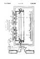
- the sole FIGUREis a cross section through a sputtering apparatus with two magnetron sputtering cathodes.
- the drawingshows the substrates 1, 1', 1" each of which is to be coated with a thin layer 2, 2', 2" of oxide (e.g. silicon dioxide or aluminum oxide).
- oxidee.g. silicon dioxide or aluminum oxide.
- the targets 3, 3a to be sputteredare located opposite theses substrates 1, 1', 1" at like distanced A 1 , A 2 .
- Each target 3, 3ais connected to a cathode base 11, 11a accommodating a magnet yoke 11b, 11ceach having three magnets 19, 19a, 19b and 19c, 19d, 19e, respectively.
- Thetargetsare made of Al, Si, Ti, Ta, Zn, Sn, Zr or compounds of these elements.
- the layers 2, 2', 2"are deposited by means of sputtering as Al 2 O 3 , AlN, SiO 2 , Si 3 N 4 , SiO x N y , TiO 2 , Ta 2 O 5 , SnO 2 , ZnO or ZrO 2 under the addition of oxygen or nitrogen, corresponding to the target material selected.
- the polarities of the poles of the six magnets which are directed toward the targetalternate so that the south poles of the two outer magnets 19, 19b and 19c, 19e together with the north poles of the respective inner magnet 10a 19a and 19d form approximate circular arc-like magnetic fields across the targets 3, 3a.
- These magnetic fieldscondense the plasma in front of the target so that it reaches its highest density where the magnetic field have the maxima of their circular arcs.
- the ions in the plasmaare accelerated by the electric fields generated by an alternating voltage supplied by power supply 10.
- the adjacent magnetron cathodes 5, 5aassociated with respective targets 3, 3aenclose an angle of 110° to180° (shown as 180° in the FIGURE).
- This power supply 10has two terminals 12, 13 formed by the two ends of a transformer secondary coil 25 and connected to the two cathodes 5 and 5a.
- the two current conductors 8, 9 of the transformer secondary coil 25are connected to respective targets 3, 3a.
- target 3via a line 14, is connected to a grounded device 20 forthe sensing of effective voltage values.
- Line 21connects this device 20 toa control 16 which in turn, via line 17, is connected to a control valve orflow regulator 18 regulating the flow of reactive gas such as oxygen or nitrogen contained in cylinder 22 to the distributing line 24 vacuum chamber 15, 15a.
- the flow of reactive gasis regulated by control 16 so that the measured voltage is identical to a desired voltage.
- Line 30connects the control 16 to a flow regulator 28 which regulates the flow ofprocess gas such as argon contained in cylinder 23 to the distributing line24.
- the cathodes 3, 3amay also be provided with respective independent distributing lines 24, 24a, with an additional control line 17a and an additional flow regulator 18a.
- Coating chamber 15, 15ahas an annular or frame-like shielding plate or diaphragm 4 which is provided with a gap or slot 6 through which the process gas from distributing line 24, in direction of the arrow, can flowinto the coating chamber 15.
- the lower edge of diaphragm 4is also surrounded by a cooling pipe 7 through which a coolant passes preventing an excessive heating of diaphragm 4.
- the frequency of the A.C. power supply 10is selected such that the ions can still follow the alternating field. This is given at a frequency between approximately 1 KHz and 100 KHz.
- the device 20 for sensing the effective value of the voltage suppliesvia line 21, supplies the discharge voltage tapped via line 14 as a direct voltage to control 16.
- Control 16in turn, via line 17, actuates magnetic valve 18 to supply reactive gas in such a manner that the measured voltagedetermines the required amount of reactive gas.
Landscapes
- Chemical & Material Sciences (AREA)
- Engineering & Computer Science (AREA)
- Chemical Kinetics & Catalysis (AREA)
- Materials Engineering (AREA)
- Mechanical Engineering (AREA)
- Metallurgy (AREA)
- Organic Chemistry (AREA)
- Physics & Mathematics (AREA)
- Plasma & Fusion (AREA)
- Analytical Chemistry (AREA)
- Physical Vapour Deposition (AREA)
Abstract
Description
Claims (5)
Applications Claiming Priority (2)
| Application Number | Priority Date | Filing Date | Title |
|---|---|---|---|
| DE4106770ADE4106770C2 (en) | 1991-03-04 | 1991-03-04 | Performing reactive coating of a substrate |
| DE4106770 | 1991-03-04 |
Publications (1)
| Publication Number | Publication Date |
|---|---|
| US5169509Atrue US5169509A (en) | 1992-12-08 |
Family
ID=6426380
Family Applications (1)
| Application Number | Title | Priority Date | Filing Date |
|---|---|---|---|
| US07/697,712Expired - LifetimeUS5169509A (en) | 1991-03-04 | 1991-05-09 | Apparatus for the reactive coating of a substrate |
Country Status (5)
| Country | Link |
|---|---|
| US (1) | US5169509A (en) |
| EP (1) | EP0502242B1 (en) |
| JP (1) | JP3363919B2 (en) |
| KR (1) | KR100239818B1 (en) |
| DE (2) | DE4106770C2 (en) |
Cited By (74)
| Publication number | Priority date | Publication date | Assignee | Title |
|---|---|---|---|---|
| US5340459A (en)* | 1991-11-22 | 1994-08-23 | Nec Corporation | Reactive sputtering system |
| US5346601A (en)* | 1993-05-11 | 1994-09-13 | Andrew Barada | Sputter coating collimator with integral reactive gas distribution |
| GB2276635A (en)* | 1993-04-01 | 1994-10-05 | Balzers Hochvakuum | Optical film material of a metal oxide |
| US5399252A (en)* | 1992-11-06 | 1995-03-21 | Leybold Aktiengesellschaft | Apparatus for coating a substrate by magnetron sputtering |
| US5415757A (en)* | 1991-11-26 | 1995-05-16 | Leybold Aktiengesellschaft | Apparatus for coating a substrate with electrically nonconductive coatings |
| GB2298654A (en)* | 1995-03-09 | 1996-09-11 | Leybold Ag | Cathod arrangement for a device for sputtering a pair of targets |
| US5558751A (en)* | 1994-04-20 | 1996-09-24 | Leybold Aktiengesellschaft | Dual cathode sputter coating apparatus |
| US5698082A (en)* | 1993-08-04 | 1997-12-16 | Balzers Und Leybold | Method and apparatus for coating substrates in a vacuum chamber, with a system for the detection and suppression of undesirable arcing |
| EP0818556A1 (en)* | 1996-07-09 | 1998-01-14 | Applied Materials, Inc. | A method for providing full-face high density plasma deposition |
| US5803973A (en)* | 1995-10-31 | 1998-09-08 | Balzers Und Leybold Deutschland Holding Ag | Apparatus for coating a substrate by chemical vapor deposition |
| US5807470A (en)* | 1995-10-06 | 1998-09-15 | Balzers Und Leybold Deutschland Holding Ag | Apparatus for coating substrates in a vacuum |
| US5812405A (en)* | 1995-05-23 | 1998-09-22 | Viratec Thin Films, Inc. | Three variable optimization system for thin film coating design |
| US5814195A (en)* | 1995-04-25 | 1998-09-29 | The Boc Group, Inc. | Sputtering system using cylindrical rotating magnetron electrically powered using alternating current |
| US5849162A (en)* | 1995-04-25 | 1998-12-15 | Deposition Sciences, Inc. | Sputtering device and method for reactive for reactive sputtering |
| US5968328A (en)* | 1996-12-11 | 1999-10-19 | Leybold Systems Gmbh | Device for sputter deposition of thin layers on flat substrates |
| US5976334A (en)* | 1997-11-25 | 1999-11-02 | Applied Materials, Inc. | Reliable sustained self-sputtering |
| US6013155A (en)* | 1996-06-28 | 2000-01-11 | Lam Research Corporation | Gas injection system for plasma processing |
| US6033483A (en)* | 1994-06-30 | 2000-03-07 | Applied Materials, Inc. | Electrically insulating sealing structure and its method of use in a high vacuum physical vapor deposition apparatus |
| US6042687A (en)* | 1997-06-30 | 2000-03-28 | Lam Research Corporation | Method and apparatus for improving etch and deposition uniformity in plasma semiconductor processing |
| US6090247A (en)* | 1994-03-19 | 2000-07-18 | Applied Vision Limited | Apparatus for coating substrates |
| US6132563A (en)* | 1995-02-24 | 2000-10-17 | Fraunhofer-Gesellschaft Zur Forderung Der Angewandten Forschung E.V. | Reactive sputtering process |
| US6168698B1 (en)* | 1995-10-27 | 2001-01-02 | Balzers Und Leybold Deutschland Holding Ag | Apparatus for coating a substrate |
| US6171454B1 (en) | 1997-09-17 | 2001-01-09 | Robert Bosch Gmbh | Method for coating surfaces using a facility having sputter electrodes |
| US6184158B1 (en) | 1996-12-23 | 2001-02-06 | Lam Research Corporation | Inductively coupled plasma CVD |
| WO2001016394A1 (en)* | 1999-09-02 | 2001-03-08 | Veeco Instruments, Inc. | Stable high rate reactive sputtering |
| US6217720B1 (en)* | 1997-06-03 | 2001-04-17 | National Research Council Of Canada | Multi-layer reactive sputtering method with reduced stabilization time |
| US6258217B1 (en)* | 1999-09-29 | 2001-07-10 | Plasma-Therm, Inc. | Rotating magnet array and sputter source |
| US6270862B1 (en) | 1996-06-28 | 2001-08-07 | Lam Research Corporation | Method for high density plasma chemical vapor deposition of dielectric films |
| US6287430B1 (en)* | 1998-07-03 | 2001-09-11 | Shincron Co., Ltd. | Apparatus and method forming thin film |
| US6361668B1 (en)* | 1996-04-29 | 2002-03-26 | Von Ardenne Anlagentechnik Gmbh | Sputtering installation with two longitudinally placed magnetrons |
| US6365010B1 (en) | 1998-11-06 | 2002-04-02 | Scivac | Sputtering apparatus and process for high rate coatings |
| US6423191B1 (en)* | 1994-02-17 | 2002-07-23 | Thin Films, Ltd. | Sputtering method and apparatus for depositing a coating onto substrate |
| US6451178B2 (en)* | 1996-10-28 | 2002-09-17 | Leybold Systems Gmbh | Interference layer system |
| US6488824B1 (en) | 1998-11-06 | 2002-12-03 | Raycom Technologies, Inc. | Sputtering apparatus and process for high rate coatings |
| US6499425B1 (en)* | 1999-01-22 | 2002-12-31 | Micron Technology, Inc. | Quasi-remote plasma processing method and apparatus |
| US20030087044A1 (en)* | 2001-11-07 | 2003-05-08 | Thomas Willms | Device for the regulation of a plasma impedance |
| US6572940B1 (en) | 1997-06-25 | 2003-06-03 | Flachglas Aktiengesellschaft | Coatings with a silver layer |
| US6605198B1 (en)* | 1993-07-22 | 2003-08-12 | Sputtered Films, Inc. | Apparatus for, and method of, depositing a film on a substrate |
| US20030201165A1 (en)* | 1999-04-23 | 2003-10-30 | Nippon Sheet Glass Co., Ltd. | Method of film deposition on substrate surface and substrate produced by the method |
| US6733642B2 (en) | 2001-04-30 | 2004-05-11 | David A. Glocker | System for unbalanced magnetron sputtering with AC power |
| US20040149575A1 (en)* | 2002-04-29 | 2004-08-05 | Isoflux, Inc. | System for unbalanced magnetron sputtering with AC power |
| US20040182701A1 (en)* | 2003-01-29 | 2004-09-23 | Aashi Glass Company, Limited | Sputtering apparatus, a mixed film produced by the sputtering apparatus and a multilayer film including the mixed film |
| US20050167264A1 (en)* | 2004-01-15 | 2005-08-04 | James Sternbergh | Method and apparatus for monitoring optical characteristics of thin films in a deposition process |
| EP1580295A1 (en)* | 2004-03-26 | 2005-09-28 | Applied Films GmbH & Co. KG | Apparatus for reactive sputtering |
| EP1584707A1 (en)* | 2004-04-08 | 2005-10-12 | Applied Films Corporation | Power coupling for high-power sputtering |
| US20060032738A1 (en)* | 2003-02-15 | 2006-02-16 | Peter Wiedemuth | Power delivery control and balancing between multiple loads |
| US20060065524A1 (en)* | 2004-09-30 | 2006-03-30 | Richard Newcomb | Non-bonded rotatable targets for sputtering |
| US20060096855A1 (en)* | 2004-11-05 | 2006-05-11 | Richard Newcomb | Cathode arrangement for atomizing a rotatable target pipe |
| US20060118412A1 (en)* | 2003-05-23 | 2006-06-08 | Jorg Krempel-Hesse | Magnetron sputter cathode |
| US20060278524A1 (en)* | 2005-06-14 | 2006-12-14 | Stowell Michael W | System and method for modulating power signals to control sputtering |
| US20060278521A1 (en)* | 2005-06-14 | 2006-12-14 | Stowell Michael W | System and method for controlling ion density and energy using modulated power signals |
| US20070098893A1 (en)* | 2005-11-01 | 2007-05-03 | Stowell Michael W | Coated substrate created by systems and methods for modulation of power and power related functions of PECVD discharge sources to achieve new film properties |
| US20070095281A1 (en)* | 2005-11-01 | 2007-05-03 | Stowell Michael W | System and method for power function ramping of microwave liner discharge sources |
| US20080087541A1 (en)* | 2004-10-18 | 2008-04-17 | Bekaert Advanced Coatings | End-Block for a Rotatable Target Sputtering Apparatus |
| WO2008049634A1 (en)* | 2006-10-26 | 2008-05-02 | Hauzer Techno Coating Bv | Dual magnetron sputtering power supply and magnetron sputtering apparatus |
| US20080245657A1 (en)* | 2006-01-25 | 2008-10-09 | Ulvac Inc. | Sputtering device and film forming method |
| WO2009052874A1 (en)* | 2007-10-26 | 2009-04-30 | Hauzer Techno Coating Bv | Dual magnetron sputtering power supply and magnetron sputtering apparatus |
| US20090159424A1 (en)* | 2007-12-19 | 2009-06-25 | Wei Liu | Dual zone gas injection nozzle |
| US20100243428A1 (en)* | 2009-03-27 | 2010-09-30 | Sputtering Components, Inc. | Rotary cathode for magnetron sputtering apparatus |
| WO2010125002A1 (en) | 2009-04-27 | 2010-11-04 | Oc Oerlikon Balzers Ag | Reactive sputtering with multiple sputter sources |
| US20110062015A1 (en)* | 2009-09-14 | 2011-03-17 | Solarworld Innovations Gmbh | Coating apparatus and coating method |
| US20120031748A1 (en)* | 2010-08-06 | 2012-02-09 | Canon Anelva Corporation | Film forming apparatus and film forming method |
| US20130098757A1 (en)* | 2010-06-17 | 2013-04-25 | Ulvac, Inc. | Sputtering deposition apparatus and adhesion preventing member |
| WO2015009864A1 (en)* | 2013-07-17 | 2015-01-22 | Advanced Energy Industries, Inc. | System and method for balancing consumption of targets in pulsed dual magnetron sputtering (dms) processes |
| US9790596B1 (en)* | 2013-01-30 | 2017-10-17 | Kyocera Corporation | Gas nozzle and plasma device employing same |
| US10208380B2 (en)* | 2015-12-04 | 2019-02-19 | Applied Materials, Inc. | Advanced coating method and materials to prevent HDP-CVD chamber arcing |
| US10395900B2 (en)* | 2016-06-17 | 2019-08-27 | Samsung Electronics Co., Ltd. | Plasma processing apparatus |
| US11053590B2 (en)* | 2014-08-15 | 2021-07-06 | Applied Materials, Inc. | Nozzle for uniform plasma processing |
| US11342164B2 (en)* | 2011-12-16 | 2022-05-24 | Taiwan Semiconductor Manufacturing Company, Ltd. | High density plasma chemical vapor deposition chamber and method of using |
| US11569070B2 (en) | 2017-06-27 | 2023-01-31 | Canon Anelva Corporation | Plasma processing apparatus |
| US11600469B2 (en) | 2017-06-27 | 2023-03-07 | Canon Anelva Corporation | Plasma processing apparatus |
| US11600466B2 (en) | 2018-06-26 | 2023-03-07 | Canon Anelva Corporation | Plasma processing apparatus, plasma processing method, and memory medium |
| US11626270B2 (en) | 2017-06-27 | 2023-04-11 | Canon Anelva Corporation | Plasma processing apparatus |
| US11961710B2 (en) | 2017-06-27 | 2024-04-16 | Canon Anelva Corporation | Plasma processing apparatus |
Families Citing this family (26)
| Publication number | Priority date | Publication date | Assignee | Title |
|---|---|---|---|---|
| DE4138793C2 (en)* | 1991-11-26 | 2001-03-01 | Leybold Ag | Method and device for coating a substrate, in particular with electrically non-conductive layers |
| DE4311360C2 (en)* | 1993-04-06 | 2002-10-24 | Applied Films Gmbh & Co Kg | Arrangement for the reactive deposition of materials as a thin film by medium frequency sputtering |
| DE69418542T2 (en)* | 1993-07-28 | 1999-09-16 | Asahi Glass Co. Ltd., Tokio/Tokyo | Process for the production of functional coatings |
| DE4326100B4 (en)* | 1993-08-04 | 2006-03-23 | Unaxis Deutschland Holding Gmbh | Method and apparatus for coating substrates in a vacuum chamber, with means for detecting and suppressing unwanted arcing |
| DE4438463C1 (en)* | 1994-10-27 | 1996-02-15 | Fraunhofer Ges Forschung | Method and circuit for bipolar pulsed energy feed to low-pressure plasmas |
| DE19540794A1 (en) | 1995-11-02 | 1997-05-07 | Leybold Ag | Device for coating a substrate from an electrically conductive target |
| DE19604454A1 (en)* | 1996-02-08 | 1997-08-14 | Balzers Prozes System Gmbh | Apparatus with two sputter cathodes for coating planar substrates |
| DE19605932A1 (en) | 1996-02-17 | 1997-08-21 | Leybold Systems Gmbh | Method for depositing an optically transparent and electrically conductive layer on a substrate made of translucent material |
| DE19703791C2 (en)* | 1997-02-01 | 2001-10-11 | Fraunhofer Ges Forschung | Process for controlling glow discharges with pulsed energy supply |
| DE19711137C1 (en)* | 1997-03-07 | 1998-08-13 | Siemens Ag | Process for applying textured YSZ layers by sputter coating |
| DE19715647C2 (en)* | 1997-04-15 | 2001-03-08 | Ardenne Anlagentech Gmbh | Method and device for regulating the reactive layer deposition on substrates by means of elongated magnetrons |
| DE59712715D1 (en)* | 1997-08-05 | 2006-10-05 | Micronas Semiconductor Holding | Adaptive filter |
| DE29717418U1 (en)* | 1997-09-26 | 1998-01-22 | Leybold Systems GmbH, 63450 Hanau | Device for applying thin layers on a substrate |
| DE19756162C2 (en)* | 1997-12-17 | 1999-10-14 | Ardenne Anlagentech Gmbh | Sputtering device |
| DE19825056C1 (en)* | 1998-06-04 | 2000-01-13 | Fraunhofer Ges Forschung | Circuit for supplying electrical energy to plasma can feed high power to unipolar or bipolar pulsed plasma with switching region in range 20 to 100 kHz with conventional IGBT switch |
| DE19827587A1 (en)* | 1998-06-20 | 1999-12-23 | Ardenne Anlagentech Gmbh | Double-magnetron sputtering unit for large area reactive plasma-enhanced deposition of e.g. light absorbing layers on metal strips for solar absorbers or heat reflective layers on window glass |
| DE19919742A1 (en)* | 1999-04-30 | 2000-11-02 | Fraunhofer Ges Forschung | Doped silicon substrates are coated with an anti-reflection layer, especially of silicon nitride for solar cells, by sputter deposition using silicon electrodes alternately connected as cathode and anode |
| DE10015244C2 (en)* | 2000-03-28 | 2002-09-19 | Fraunhofer Ges Forschung | Method and circuit arrangement for pulsed energy feed in magnetron discharges |
| DE10122431A1 (en)* | 2001-05-09 | 2002-11-28 | Fraunhofer Ges Forschung | Electrode arrangement for the magnetic field-guided plasma-assisted deposition of thin layers in a vacuum |
| DE10224128A1 (en)* | 2002-05-29 | 2003-12-18 | Schmid Rhyner Ag Adliswil | Method of applying coatings to surfaces |
| JP3866615B2 (en) | 2002-05-29 | 2007-01-10 | 株式会社神戸製鋼所 | Reactive sputtering method and apparatus |
| US7967957B2 (en) | 2002-08-09 | 2011-06-28 | Kobe Steel, Ltd. | Method for preparing alumna coating film having alpha-type crystal structure as primary structure |
| JP2006045611A (en)* | 2004-08-04 | 2006-02-16 | Nippon Telegr & Teleph Corp <Ntt> | Sputter deposition system |
| JP5256475B2 (en)* | 2011-02-10 | 2013-08-07 | 株式会社ユーテック | Opposing target type sputtering apparatus and opposing target type sputtering method |
| JP6101533B2 (en)* | 2013-03-27 | 2017-03-22 | 株式会社Screenホールディングス | Aluminum oxide film formation method |
| DE102016118799B4 (en) | 2016-10-05 | 2022-08-11 | VON ARDENNE Asset GmbH & Co. KG | Magnetron sputtering process |
Citations (10)
| Publication number | Priority date | Publication date | Assignee | Title |
|---|---|---|---|---|
| GB1172106A (en)* | 1967-06-29 | 1969-11-26 | Edwards High Vacuum Int Ltd | Improvements in or relating to Pressure Control in Vacuum Apparatus |
| FR95311E (en)* | 1967-03-24 | 1970-08-21 | Varian Associates | Cathode sputtering apparatus for depositing thin films on surfaces to be coated. |
| US3860507A (en)* | 1972-11-29 | 1975-01-14 | Rca Corp | Rf sputtering apparatus and method |
| US4166784A (en)* | 1978-04-28 | 1979-09-04 | Applied Films Lab, Inc. | Feedback control for vacuum deposition apparatus |
| JPS61179864A (en)* | 1985-02-06 | 1986-08-12 | Hitachi Ltd | Sputtering device |
| DD252205A1 (en)* | 1986-09-01 | 1987-12-09 | Ardenne Forschungsinst | atomizing |
| US4738761A (en)* | 1986-10-06 | 1988-04-19 | Microelectronics Center Of North Carolina | Shared current loop, multiple field apparatus and process for plasma processing |
| DE3802852A1 (en)* | 1988-02-01 | 1989-08-03 | Leybold Ag | Device for coating a substrate with a material obtained from a plasma |
| DE3912572A1 (en)* | 1988-04-20 | 1989-11-02 | Fuji Photo Film Co Ltd | SPRAYING DEVICE |
| US4981566A (en)* | 1989-08-02 | 1991-01-01 | Leybold Aktiengesellschaft | Arrangement for measuring the thickness of thin layers |
- 1991
- 1991-03-04DEDE4106770Apatent/DE4106770C2/ennot_activeExpired - Lifetime
- 1991-05-09USUS07/697,712patent/US5169509A/ennot_activeExpired - Lifetime
- 1991-09-25DEDE59108836Tpatent/DE59108836D1/ennot_activeExpired - Lifetime
- 1991-09-25EPEP91116294Apatent/EP0502242B1/ennot_activeExpired - Lifetime
- 1991-10-14KRKR1019910018055Apatent/KR100239818B1/ennot_activeExpired - Lifetime
- 1992
- 1992-03-03JPJP04517592Apatent/JP3363919B2/ennot_activeExpired - Lifetime
Patent Citations (11)
| Publication number | Priority date | Publication date | Assignee | Title |
|---|---|---|---|---|
| FR95311E (en)* | 1967-03-24 | 1970-08-21 | Varian Associates | Cathode sputtering apparatus for depositing thin films on surfaces to be coated. |
| GB1172106A (en)* | 1967-06-29 | 1969-11-26 | Edwards High Vacuum Int Ltd | Improvements in or relating to Pressure Control in Vacuum Apparatus |
| US3860507A (en)* | 1972-11-29 | 1975-01-14 | Rca Corp | Rf sputtering apparatus and method |
| US4166784A (en)* | 1978-04-28 | 1979-09-04 | Applied Films Lab, Inc. | Feedback control for vacuum deposition apparatus |
| JPS61179864A (en)* | 1985-02-06 | 1986-08-12 | Hitachi Ltd | Sputtering device |
| DD252205A1 (en)* | 1986-09-01 | 1987-12-09 | Ardenne Forschungsinst | atomizing |
| US4738761A (en)* | 1986-10-06 | 1988-04-19 | Microelectronics Center Of North Carolina | Shared current loop, multiple field apparatus and process for plasma processing |
| DE3802852A1 (en)* | 1988-02-01 | 1989-08-03 | Leybold Ag | Device for coating a substrate with a material obtained from a plasma |
| DE3912572A1 (en)* | 1988-04-20 | 1989-11-02 | Fuji Photo Film Co Ltd | SPRAYING DEVICE |
| US4956070A (en)* | 1988-04-20 | 1990-09-11 | Fuji Photo Film Co., Ltd. | Sputtering apparatus |
| US4981566A (en)* | 1989-08-02 | 1991-01-01 | Leybold Aktiengesellschaft | Arrangement for measuring the thickness of thin layers |
Cited By (107)
| Publication number | Priority date | Publication date | Assignee | Title |
|---|---|---|---|---|
| US5340459A (en)* | 1991-11-22 | 1994-08-23 | Nec Corporation | Reactive sputtering system |
| US5415757A (en)* | 1991-11-26 | 1995-05-16 | Leybold Aktiengesellschaft | Apparatus for coating a substrate with electrically nonconductive coatings |
| US5399252A (en)* | 1992-11-06 | 1995-03-21 | Leybold Aktiengesellschaft | Apparatus for coating a substrate by magnetron sputtering |
| US6506288B1 (en) | 1993-01-04 | 2003-01-14 | Unaxis Balzers Aktiengesellschaft | Optical film material especially TiO2 or Ta2O5 optical waveguide layer and method for producing such |
| GB2276635A (en)* | 1993-04-01 | 1994-10-05 | Balzers Hochvakuum | Optical film material of a metal oxide |
| GB2276635B (en)* | 1993-04-01 | 1997-04-16 | Balzers Hochvakuum | Optical film material,especially TiOÂ or TaÂO5,optical waveguide layer and method for producing such |
| US5346601A (en)* | 1993-05-11 | 1994-09-13 | Andrew Barada | Sputter coating collimator with integral reactive gas distribution |
| US6605198B1 (en)* | 1993-07-22 | 2003-08-12 | Sputtered Films, Inc. | Apparatus for, and method of, depositing a film on a substrate |
| US5698082A (en)* | 1993-08-04 | 1997-12-16 | Balzers Und Leybold | Method and apparatus for coating substrates in a vacuum chamber, with a system for the detection and suppression of undesirable arcing |
| US6423191B1 (en)* | 1994-02-17 | 2002-07-23 | Thin Films, Ltd. | Sputtering method and apparatus for depositing a coating onto substrate |
| US6090247A (en)* | 1994-03-19 | 2000-07-18 | Applied Vision Limited | Apparatus for coating substrates |
| US5558751A (en)* | 1994-04-20 | 1996-09-24 | Leybold Aktiengesellschaft | Dual cathode sputter coating apparatus |
| US6033483A (en)* | 1994-06-30 | 2000-03-07 | Applied Materials, Inc. | Electrically insulating sealing structure and its method of use in a high vacuum physical vapor deposition apparatus |
| US20020187271A1 (en)* | 1994-06-30 | 2002-12-12 | Demaray Richard Ernest | Method of forming an electrically insulating sealing structure for use in a semiconductor manufacturing apparatus |
| US6436509B1 (en) | 1994-06-30 | 2002-08-20 | Applied Materials, Inc. | Electrically insulating sealing structure and its method of use in a semiconductor manufacturing apparatus |
| US6821562B2 (en)* | 1994-06-30 | 2004-11-23 | Applied Materials, Inc. | Method of forming an electrically insulating sealing structure for use in a semiconductor manufacturing apparatus |
| US6132563A (en)* | 1995-02-24 | 2000-10-17 | Fraunhofer-Gesellschaft Zur Forderung Der Angewandten Forschung E.V. | Reactive sputtering process |
| GB2298654A (en)* | 1995-03-09 | 1996-09-11 | Leybold Ag | Cathod arrangement for a device for sputtering a pair of targets |
| GB2298654B (en)* | 1995-03-09 | 1998-07-15 | Leybold Ag | Cathode arrangement for a device for sputtering a pair of targets |
| US5849162A (en)* | 1995-04-25 | 1998-12-15 | Deposition Sciences, Inc. | Sputtering device and method for reactive for reactive sputtering |
| US5814195A (en)* | 1995-04-25 | 1998-09-29 | The Boc Group, Inc. | Sputtering system using cylindrical rotating magnetron electrically powered using alternating current |
| US5812405A (en)* | 1995-05-23 | 1998-09-22 | Viratec Thin Films, Inc. | Three variable optimization system for thin film coating design |
| US5807470A (en)* | 1995-10-06 | 1998-09-15 | Balzers Und Leybold Deutschland Holding Ag | Apparatus for coating substrates in a vacuum |
| US6168698B1 (en)* | 1995-10-27 | 2001-01-02 | Balzers Und Leybold Deutschland Holding Ag | Apparatus for coating a substrate |
| US5803973A (en)* | 1995-10-31 | 1998-09-08 | Balzers Und Leybold Deutschland Holding Ag | Apparatus for coating a substrate by chemical vapor deposition |
| US6361668B1 (en)* | 1996-04-29 | 2002-03-26 | Von Ardenne Anlagentechnik Gmbh | Sputtering installation with two longitudinally placed magnetrons |
| US6013155A (en)* | 1996-06-28 | 2000-01-11 | Lam Research Corporation | Gas injection system for plasma processing |
| US6270862B1 (en) | 1996-06-28 | 2001-08-07 | Lam Research Corporation | Method for high density plasma chemical vapor deposition of dielectric films |
| EP0818556A1 (en)* | 1996-07-09 | 1998-01-14 | Applied Materials, Inc. | A method for providing full-face high density plasma deposition |
| US6814839B2 (en)* | 1996-10-28 | 2004-11-09 | Unaxis Deutschland Holding Gmbh | Interference layer system |
| US6451178B2 (en)* | 1996-10-28 | 2002-09-17 | Leybold Systems Gmbh | Interference layer system |
| US5968328A (en)* | 1996-12-11 | 1999-10-19 | Leybold Systems Gmbh | Device for sputter deposition of thin layers on flat substrates |
| US20010019903A1 (en)* | 1996-12-23 | 2001-09-06 | Paul Kevin Shufflebotham | Inductively coupled plasma CVD |
| US6184158B1 (en) | 1996-12-23 | 2001-02-06 | Lam Research Corporation | Inductively coupled plasma CVD |
| US6217720B1 (en)* | 1997-06-03 | 2001-04-17 | National Research Council Of Canada | Multi-layer reactive sputtering method with reduced stabilization time |
| US6572940B1 (en) | 1997-06-25 | 2003-06-03 | Flachglas Aktiengesellschaft | Coatings with a silver layer |
| US6042687A (en)* | 1997-06-30 | 2000-03-28 | Lam Research Corporation | Method and apparatus for improving etch and deposition uniformity in plasma semiconductor processing |
| DE19740793C2 (en)* | 1997-09-17 | 2003-03-20 | Bosch Gmbh Robert | Process for coating surfaces by means of a system with sputter electrodes and use of the process |
| US6171454B1 (en) | 1997-09-17 | 2001-01-09 | Robert Bosch Gmbh | Method for coating surfaces using a facility having sputter electrodes |
| US5976334A (en)* | 1997-11-25 | 1999-11-02 | Applied Materials, Inc. | Reliable sustained self-sputtering |
| US6287430B1 (en)* | 1998-07-03 | 2001-09-11 | Shincron Co., Ltd. | Apparatus and method forming thin film |
| US6365010B1 (en) | 1998-11-06 | 2002-04-02 | Scivac | Sputtering apparatus and process for high rate coatings |
| US6488824B1 (en) | 1998-11-06 | 2002-12-03 | Raycom Technologies, Inc. | Sputtering apparatus and process for high rate coatings |
| US6499425B1 (en)* | 1999-01-22 | 2002-12-31 | Micron Technology, Inc. | Quasi-remote plasma processing method and apparatus |
| US20030201165A1 (en)* | 1999-04-23 | 2003-10-30 | Nippon Sheet Glass Co., Ltd. | Method of film deposition on substrate surface and substrate produced by the method |
| WO2001016394A1 (en)* | 1999-09-02 | 2001-03-08 | Veeco Instruments, Inc. | Stable high rate reactive sputtering |
| US6258217B1 (en)* | 1999-09-29 | 2001-07-10 | Plasma-Therm, Inc. | Rotating magnet array and sputter source |
| US6733642B2 (en) | 2001-04-30 | 2004-05-11 | David A. Glocker | System for unbalanced magnetron sputtering with AC power |
| US20030087044A1 (en)* | 2001-11-07 | 2003-05-08 | Thomas Willms | Device for the regulation of a plasma impedance |
| US6860973B2 (en) | 2001-11-07 | 2005-03-01 | Applied Films Gmbh & Co. Kg. | Device for the regulation of a plasma impedance |
| US20040149575A1 (en)* | 2002-04-29 | 2004-08-05 | Isoflux, Inc. | System for unbalanced magnetron sputtering with AC power |
| US20040182701A1 (en)* | 2003-01-29 | 2004-09-23 | Aashi Glass Company, Limited | Sputtering apparatus, a mixed film produced by the sputtering apparatus and a multilayer film including the mixed film |
| US20060032738A1 (en)* | 2003-02-15 | 2006-02-16 | Peter Wiedemuth | Power delivery control and balancing between multiple loads |
| US7586210B2 (en) | 2003-02-15 | 2009-09-08 | Huettinger Elektronik Gmbh + Co. Kg | Power delivery control and balancing between multiple loads |
| US20080048498A1 (en)* | 2003-02-15 | 2008-02-28 | Huettinger Elektronik Gmbh + Co. Kg | Power Delivery Control and Balancing Between Multiple Loads |
| US8715471B2 (en) | 2003-05-23 | 2014-05-06 | Applied Materials Gmbh & Co Kg | Magnetron sputter cathode |
| US20060118412A1 (en)* | 2003-05-23 | 2006-06-08 | Jorg Krempel-Hesse | Magnetron sputter cathode |
| US20050167264A1 (en)* | 2004-01-15 | 2005-08-04 | James Sternbergh | Method and apparatus for monitoring optical characteristics of thin films in a deposition process |
| US7008518B2 (en) | 2004-01-15 | 2006-03-07 | Deposition Sciences, Inc. | Method and apparatus for monitoring optical characteristics of thin films in a deposition process |
| US20050211550A1 (en)* | 2004-03-26 | 2005-09-29 | Thomas Fritz | Device for reactive sputtering |
| EP1580295A1 (en)* | 2004-03-26 | 2005-09-28 | Applied Films GmbH & Co. KG | Apparatus for reactive sputtering |
| EP1584707A1 (en)* | 2004-04-08 | 2005-10-12 | Applied Films Corporation | Power coupling for high-power sputtering |
| US20050224343A1 (en)* | 2004-04-08 | 2005-10-13 | Richard Newcomb | Power coupling for high-power sputtering |
| US20060065524A1 (en)* | 2004-09-30 | 2006-03-30 | Richard Newcomb | Non-bonded rotatable targets for sputtering |
| US20080087541A1 (en)* | 2004-10-18 | 2008-04-17 | Bekaert Advanced Coatings | End-Block for a Rotatable Target Sputtering Apparatus |
| US7824528B2 (en) | 2004-10-18 | 2010-11-02 | Bekaert Advanced Coatings | End-block for a rotatable target sputtering apparatus |
| US20060096855A1 (en)* | 2004-11-05 | 2006-05-11 | Richard Newcomb | Cathode arrangement for atomizing a rotatable target pipe |
| US20060278521A1 (en)* | 2005-06-14 | 2006-12-14 | Stowell Michael W | System and method for controlling ion density and energy using modulated power signals |
| US20060278524A1 (en)* | 2005-06-14 | 2006-12-14 | Stowell Michael W | System and method for modulating power signals to control sputtering |
| US20070098916A1 (en)* | 2005-11-01 | 2007-05-03 | Stowell Michael W | System and method for modulation of power and power related functions of PECVD discharge sources to achieve new film properties |
| US20080286495A1 (en)* | 2005-11-01 | 2008-11-20 | Stowell Michael W | System and method for power function ramping of split antenna pecvd discharge sources |
| US20070098893A1 (en)* | 2005-11-01 | 2007-05-03 | Stowell Michael W | Coated substrate created by systems and methods for modulation of power and power related functions of PECVD discharge sources to achieve new film properties |
| US20070095281A1 (en)* | 2005-11-01 | 2007-05-03 | Stowell Michael W | System and method for power function ramping of microwave liner discharge sources |
| US7842355B2 (en) | 2005-11-01 | 2010-11-30 | Applied Materials, Inc. | System and method for modulation of power and power related functions of PECVD discharge sources to achieve new film properties |
| US20080245657A1 (en)* | 2006-01-25 | 2008-10-09 | Ulvac Inc. | Sputtering device and film forming method |
| EP1978127A4 (en)* | 2006-01-25 | 2012-06-20 | Ulvac Inc | Spattering device and film forming method |
| US8147657B2 (en)* | 2006-01-25 | 2012-04-03 | Ulvac, Inc. | Sputtering device and film forming method |
| WO2008049634A1 (en)* | 2006-10-26 | 2008-05-02 | Hauzer Techno Coating Bv | Dual magnetron sputtering power supply and magnetron sputtering apparatus |
| US20100140083A1 (en)* | 2006-10-26 | 2010-06-10 | Hauzer Techno Coating Bv | Dual Magnetron Sputtering Power Supply And Magnetron Sputtering Apparatus |
| WO2009052874A1 (en)* | 2007-10-26 | 2009-04-30 | Hauzer Techno Coating Bv | Dual magnetron sputtering power supply and magnetron sputtering apparatus |
| US8137463B2 (en)* | 2007-12-19 | 2012-03-20 | Applied Materials, Inc. | Dual zone gas injection nozzle |
| US20090159424A1 (en)* | 2007-12-19 | 2009-06-25 | Wei Liu | Dual zone gas injection nozzle |
| US8182662B2 (en) | 2009-03-27 | 2012-05-22 | Sputtering Components, Inc. | Rotary cathode for magnetron sputtering apparatus |
| US20100243428A1 (en)* | 2009-03-27 | 2010-09-30 | Sputtering Components, Inc. | Rotary cathode for magnetron sputtering apparatus |
| WO2010125002A1 (en) | 2009-04-27 | 2010-11-04 | Oc Oerlikon Balzers Ag | Reactive sputtering with multiple sputter sources |
| US20110062015A1 (en)* | 2009-09-14 | 2011-03-17 | Solarworld Innovations Gmbh | Coating apparatus and coating method |
| US20130098757A1 (en)* | 2010-06-17 | 2013-04-25 | Ulvac, Inc. | Sputtering deposition apparatus and adhesion preventing member |
| US20120031748A1 (en)* | 2010-08-06 | 2012-02-09 | Canon Anelva Corporation | Film forming apparatus and film forming method |
| US9175377B2 (en)* | 2010-08-06 | 2015-11-03 | Canon Anelva Corporation | Film forming apparatus and film forming method |
| US12020905B2 (en) | 2011-12-16 | 2024-06-25 | Taiwan Semiconductor Manufacturing Company, Ltd. | Method of using high density plasma chemical vapor deposition chamber |
| US11342164B2 (en)* | 2011-12-16 | 2022-05-24 | Taiwan Semiconductor Manufacturing Company, Ltd. | High density plasma chemical vapor deposition chamber and method of using |
| US9790596B1 (en)* | 2013-01-30 | 2017-10-17 | Kyocera Corporation | Gas nozzle and plasma device employing same |
| US10332730B2 (en) | 2013-07-17 | 2019-06-25 | Aes Global Holdings, Pte. Ltd | Method for balancing consumption of targets in pulsed dual magnetron sputtering (DMS) processes |
| WO2015009864A1 (en)* | 2013-07-17 | 2015-01-22 | Advanced Energy Industries, Inc. | System and method for balancing consumption of targets in pulsed dual magnetron sputtering (dms) processes |
| US9711335B2 (en) | 2013-07-17 | 2017-07-18 | Advanced Energy Industries, Inc. | System and method for balancing consumption of targets in pulsed dual magnetron sputtering (DMS) processes |
| US11053590B2 (en)* | 2014-08-15 | 2021-07-06 | Applied Materials, Inc. | Nozzle for uniform plasma processing |
| US10655223B2 (en)* | 2015-12-04 | 2020-05-19 | Applied Materials, Inc. | Advanced coating method and materials to prevent HDP-CVD chamber arcing |
| US10208380B2 (en)* | 2015-12-04 | 2019-02-19 | Applied Materials, Inc. | Advanced coating method and materials to prevent HDP-CVD chamber arcing |
| US10395900B2 (en)* | 2016-06-17 | 2019-08-27 | Samsung Electronics Co., Ltd. | Plasma processing apparatus |
| US10903053B2 (en)* | 2016-06-17 | 2021-01-26 | Samsung Electronics Co., Ltd. | Plasma processing apparatus |
| US11569070B2 (en) | 2017-06-27 | 2023-01-31 | Canon Anelva Corporation | Plasma processing apparatus |
| US11626270B2 (en) | 2017-06-27 | 2023-04-11 | Canon Anelva Corporation | Plasma processing apparatus |
| US11756773B2 (en) | 2017-06-27 | 2023-09-12 | Canon Anelva Corporation | Plasma processing apparatus |
| US11784030B2 (en)* | 2017-06-27 | 2023-10-10 | Canon Anelva Corporation | Plasma processing apparatus |
| US11961710B2 (en) | 2017-06-27 | 2024-04-16 | Canon Anelva Corporation | Plasma processing apparatus |
| US11600469B2 (en) | 2017-06-27 | 2023-03-07 | Canon Anelva Corporation | Plasma processing apparatus |
| US11600466B2 (en) | 2018-06-26 | 2023-03-07 | Canon Anelva Corporation | Plasma processing apparatus, plasma processing method, and memory medium |
Also Published As
| Publication number | Publication date |
|---|---|
| EP0502242A3 (en) | 1993-12-15 |
| JP3363919B2 (en) | 2003-01-08 |
| JPH04325680A (en) | 1992-11-16 |
| DE4106770A1 (en) | 1992-09-10 |
| DE4106770C2 (en) | 1996-10-17 |
| DE59108836D1 (en) | 1997-10-02 |
| KR930008185A (en) | 1993-05-21 |
| EP0502242A2 (en) | 1992-09-09 |
| EP0502242B1 (en) | 1997-08-27 |
| KR100239818B1 (en) | 2000-01-15 |
Similar Documents
| Publication | Publication Date | Title |
|---|---|---|
| US5169509A (en) | Apparatus for the reactive coating of a substrate | |
| US5399252A (en) | Apparatus for coating a substrate by magnetron sputtering | |
| US5026471A (en) | Device for coating a substrate | |
| US5126033A (en) | Process and apparatus for reactively coating a substrate | |
| US5126032A (en) | Process and apparatus for reactively coating a substrate | |
| US5082546A (en) | Apparatus for the reactive coating of a substrate | |
| US5616225A (en) | Use of multiple anodes in a magnetron for improving the uniformity of its plasma | |
| JP2936276B2 (en) | Method and apparatus for manufacturing transparent conductive film | |
| US6113752A (en) | Method and device for coating substrate | |
| US5556520A (en) | Method for controlling a reactive sputtering process | |
| US5803973A (en) | Apparatus for coating a substrate by chemical vapor deposition | |
| US20090308732A1 (en) | Apparatus and method for uniform deposition | |
| US5006213A (en) | Process for coating a substrate with electrically conductive materials | |
| GB1489807A (en) | Method for coating a substrate | |
| US5718815A (en) | Apparatus for coating a substrate from an electrically conductive target | |
| US5861088A (en) | Magnetic field cathode | |
| US5167789A (en) | Apparatus for coating a substrate | |
| CA2184432C (en) | Apparatus for coating substrates in a vacuum | |
| US20010006148A1 (en) | Interference layer system | |
| JPH11269643A (en) | Film forming apparatus and film forming method using the same | |
| KR100238786B1 (en) | Process for depositing an optical transparent and electrical conductive on a substrate of transparent material | |
| US5240584A (en) | Apparatus for the reactive coating of a substrate | |
| US20050211550A1 (en) | Device for reactive sputtering | |
| JPH09176840A (en) | Vacuum coating apparatus | |
| KR102647736B1 (en) | Sputtering apparatus and sputtering method using the same |
Legal Events
| Date | Code | Title | Description |
|---|---|---|---|
| AS | Assignment | Owner name:LEYBOLD AKTIENGESELLSCHAFT Free format text:ASSIGNMENT OF ASSIGNORS INTEREST.;ASSIGNORS:LATZ, RUDOLF;SCHANZ, MICHAEL;SCHERER, MICHAEL;AND OTHERS;REEL/FRAME:005765/0514 Effective date:19910417 | |
| STCF | Information on status: patent grant | Free format text:PATENTED CASE | |
| FEPP | Fee payment procedure | Free format text:PAYOR NUMBER ASSIGNED (ORIGINAL EVENT CODE: ASPN); ENTITY STATUS OF PATENT OWNER: LARGE ENTITY | |
| FPAY | Fee payment | Year of fee payment:4 | |
| AS | Assignment | Owner name:BALZERS UND LEYBOLD DEUTSCHLAND HOLDING AKTIENGESE Free format text:CHANGE OF NAME;ASSIGNOR:LEYBOLD AKTIENGESELLSCHAFT;REEL/FRAME:008447/0925 Effective date:19960821 | |
| FPAY | Fee payment | Year of fee payment:8 | |
| FEPP | Fee payment procedure | Free format text:PAYER NUMBER DE-ASSIGNED (ORIGINAL EVENT CODE: RMPN); ENTITY STATUS OF PATENT OWNER: LARGE ENTITY Free format text:PAYOR NUMBER ASSIGNED (ORIGINAL EVENT CODE: ASPN); ENTITY STATUS OF PATENT OWNER: LARGE ENTITY | |
| FPAY | Fee payment | Year of fee payment:12 |