US5168534A - Cascaded optic modulator arrangement - Google Patents
Cascaded optic modulator arrangementDownload PDFInfo
- Publication number
- US5168534A US5168534AUS07/803,818US80381891AUS5168534AUS 5168534 AUS5168534 AUS 5168534AUS 80381891 AUS80381891 AUS 80381891AUS 5168534 AUS5168534 AUS 5168534A
- Authority
- US
- United States
- Prior art keywords
- waveguide
- waveguide means
- modulator
- energy
- pair
- Prior art date
- Legal status (The legal status is an assumption and is not a legal conclusion. Google has not performed a legal analysis and makes no representation as to the accuracy of the status listed.)
- Expired - Lifetime
Links
- 230000004044responseEffects0.000claimsabstractdescription10
- 239000000758substrateSubstances0.000claimsdescription6
- 239000000463materialSubstances0.000claimsdescription4
- WSMQKESQZFQMFW-UHFFFAOYSA-N5-methyl-pyrazole-3-carboxylic acidChemical compoundCC1=CC(C(O)=O)=NN1WSMQKESQZFQMFW-UHFFFAOYSA-N0.000claimsdescription3
- GQYHUHYESMUTHG-UHFFFAOYSA-Nlithium niobateChemical compound[Li+].[O-][Nb](=O)=OGQYHUHYESMUTHG-UHFFFAOYSA-N0.000claimsdescription3
- 230000001902propagating effectEffects0.000claims9
- 238000000034methodMethods0.000abstractdescription6
- 230000008569processEffects0.000abstractdescription4
- 230000003287optical effectEffects0.000description60
- 230000009467reductionEffects0.000description6
- 230000005540biological transmissionEffects0.000description4
- 230000000694effectsEffects0.000description4
- 230000005684electric fieldEffects0.000description4
- 238000004891communicationMethods0.000description3
- 229910003327LiNbO3Inorganic materials0.000description2
- 229910012463LiTaO3Inorganic materials0.000description2
- 238000007792additionMethods0.000description2
- 230000008901benefitEffects0.000description2
- 239000002131composite materialSubstances0.000description2
- 238000010586diagramMethods0.000description2
- 238000005516engineering processMethods0.000description2
- 230000006872improvementEffects0.000description2
- RTAQQCXQSZGOHL-UHFFFAOYSA-NTitaniumChemical compound[Ti]RTAQQCXQSZGOHL-UHFFFAOYSA-N0.000description1
- 239000000969carrierSubstances0.000description1
- 230000001427coherent effectEffects0.000description1
- 230000001934delayEffects0.000description1
- 239000006185dispersionSubstances0.000description1
- 239000000835fiberSubstances0.000description1
- 238000002044microwave spectrumMethods0.000description1
- 239000013307optical fiberSubstances0.000description1
- 239000004065semiconductorSubstances0.000description1
- 238000000926separation methodMethods0.000description1
- 239000007787solidSubstances0.000description1
- 238000001228spectrumMethods0.000description1
- 230000001360synchronised effectEffects0.000description1
- 229910052719titaniumInorganic materials0.000description1
- 239000010936titaniumSubstances0.000description1
Images


Classifications
- G—PHYSICS
- G02—OPTICS
- G02F—OPTICAL DEVICES OR ARRANGEMENTS FOR THE CONTROL OF LIGHT BY MODIFICATION OF THE OPTICAL PROPERTIES OF THE MEDIA OF THE ELEMENTS INVOLVED THEREIN; NON-LINEAR OPTICS; FREQUENCY-CHANGING OF LIGHT; OPTICAL LOGIC ELEMENTS; OPTICAL ANALOGUE/DIGITAL CONVERTERS
- G02F1/00—Devices or arrangements for the control of the intensity, colour, phase, polarisation or direction of light arriving from an independent light source, e.g. switching, gating or modulating; Non-linear optics
- G02F1/01—Devices or arrangements for the control of the intensity, colour, phase, polarisation or direction of light arriving from an independent light source, e.g. switching, gating or modulating; Non-linear optics for the control of the intensity, phase, polarisation or colour
- G02F1/21—Devices or arrangements for the control of the intensity, colour, phase, polarisation or direction of light arriving from an independent light source, e.g. switching, gating or modulating; Non-linear optics for the control of the intensity, phase, polarisation or colour by interference
- G02F1/225—Devices or arrangements for the control of the intensity, colour, phase, polarisation or direction of light arriving from an independent light source, e.g. switching, gating or modulating; Non-linear optics for the control of the intensity, phase, polarisation or colour by interference in an optical waveguide structure
- G—PHYSICS
- G02—OPTICS
- G02B—OPTICAL ELEMENTS, SYSTEMS OR APPARATUS
- G02B6/00—Light guides; Structural details of arrangements comprising light guides and other optical elements, e.g. couplings
- G02B6/10—Light guides; Structural details of arrangements comprising light guides and other optical elements, e.g. couplings of the optical waveguide type
- G02B6/12—Light guides; Structural details of arrangements comprising light guides and other optical elements, e.g. couplings of the optical waveguide type of the integrated circuit kind
- G02B6/12004—Combinations of two or more optical elements
- G—PHYSICS
- G02—OPTICS
- G02F—OPTICAL DEVICES OR ARRANGEMENTS FOR THE CONTROL OF LIGHT BY MODIFICATION OF THE OPTICAL PROPERTIES OF THE MEDIA OF THE ELEMENTS INVOLVED THEREIN; NON-LINEAR OPTICS; FREQUENCY-CHANGING OF LIGHT; OPTICAL LOGIC ELEMENTS; OPTICAL ANALOGUE/DIGITAL CONVERTERS
- G02F1/00—Devices or arrangements for the control of the intensity, colour, phase, polarisation or direction of light arriving from an independent light source, e.g. switching, gating or modulating; Non-linear optics
- G02F1/01—Devices or arrangements for the control of the intensity, colour, phase, polarisation or direction of light arriving from an independent light source, e.g. switching, gating or modulating; Non-linear optics for the control of the intensity, phase, polarisation or colour
- G02F1/0121—Operation of devices; Circuit arrangements, not otherwise provided for in this subclass
- G02F1/0123—Circuits for the control or stabilisation of the bias voltage, e.g. automatic bias control [ABC] feedback loops
- G—PHYSICS
- G02—OPTICS
- G02F—OPTICAL DEVICES OR ARRANGEMENTS FOR THE CONTROL OF LIGHT BY MODIFICATION OF THE OPTICAL PROPERTIES OF THE MEDIA OF THE ELEMENTS INVOLVED THEREIN; NON-LINEAR OPTICS; FREQUENCY-CHANGING OF LIGHT; OPTICAL LOGIC ELEMENTS; OPTICAL ANALOGUE/DIGITAL CONVERTERS
- G02F2203/00—Function characteristic
- G02F2203/19—Function characteristic linearised modulation; reduction of harmonic distortions
Definitions
- This inventionrelates to optic modulators, and more particularly to a cascaded optic modulator arrangement for improved modulator linear response.
- a trend in optical communication systemsis to integrate functions traditionally performed by discrete optical components onto an integrated optic ("IO") device. These functions include polarizers, filters, modulators, directional couplers, waveguides, etc.
- the IO deviceis typically fabricated from a substrate of lithium niobate, LiNbO 3 , or lithium tantalate, LiTaO 3 , and has a waveguide formed on a major surface. Common waveguides include the Mach-Zehnder and Balanced-Bridge interferometers. In the Mach-Zehnder, an input optical signal from, e.g., a laser light source, is split at a Y-junction in the waveguide into two equal components. Each component travels in a corresponding arm of the waveguide before being recombined at a second Y-junction.
- one or more electrooptic modulatorscomprising electrodes are formed on the waveguide surface in the vicinity of the arms.
- a time varying voltage applied to the electrodesproduces an electric field in the IO device substrate.
- “Mach-Zehnder”refers to the waveguide Y-junctions and arms, along with the modulators.
- the electric fieldeffectively changes the relative indices of refraction, and, thus, the optical path lengths, of the waveguide arms.
- Modulation of the optical input signaloccurs since the relative phase of the optical signals in the arms varies according to the instantaneous amplitude of the time varying electrical signal driving the electrodes.
- the varying phaseresults in a varying amplitude of the intensity of the optical signal at the interferometer output.
- the modulatorSince the modulator operates on light interference principles, its transfer function is a nonlinear cosine curve. When used to modulate radio frequency energy ("RF"), the modulator then generates undesirable harmonics. When the modulator is driven symmetrically about the optical half intensity point of the cosine curve (i.e., the approximate linear region of the curve), fundamental and odd harmonics predominate in the Mach-Zehnder's output. The amplitudes of the higher harmonics increase as the modulating voltage is increased. Thus, the Mach-Zehnder's output deviates noticeably from that which would be obtained with a perfectly linear device. When the modulator is biased such that the optical output is either at a maximum or minimum, even harmonics predominate and the power in the fundamental drops to zero.
- RFradio frequency energy
- This harmonic intermodulation distortionis a problem in a multichannel optical communication system, e.g., cable television ("CATV").
- a CATV systemmay have 75 channels multiplexed for transmission in a frequency range of 50-500 MHz.
- the large number of closely-spaced carriersplaces strict requirements on the linearity of system elements in order to reduce undesired harmonic distortions.
- the inherent cosine response of an electrooptic modulatordoes not provide the requisite linearity.
- the intercarrier separationmay be increased; however, this is an inefficient use of the allotted frequency spectrum.
- Typical amplitude modulation (AM) transmission requirements for second and third order harmonicsare -60dBc relative to the fundamental.
- Optical linearization schemesare known in which two parallel Mach-Zehnders achieve incoherent combination of light intensities. For example, see Lin, Z.-Q. et al., "Reduction of Intermodulation Distortion of Interferometric Optical Modulators Through Incoherent Mixing of Optical Waves", Electronics Letters, 1990, Vol. 26, No. 23, pp. 1980-1982. However, such a scheme provides only 30 to 40 dB of distortion reduction. Further, its usefulness may be limited to moderate modulation frequency and transmission distance, from wavelength dispersion.
- An exemplary predistortion circuitconsists of a nonlinear device which generates distortion products which are equal in amplitude, but opposite in phase with the distortion products produced by the modulator. (See Childs, R. B. et al., "Predistortion Linearization of Directly Modulated DFB Lasers and External Modulators for AM Radio Transmission", Technical Digest, Optical Fiber Communication Conf., Optical Society of America, Wash. D.C., 1990, paper WH-6).
- An exemplary feedforward schemeis Saleh, A. M.
- Objects of the present inventioninclude provision of improved linearity in the transfer function of an arrangement of electrooptic modulators.
- two optic interferometerssuch as Mach-Zehnders
- Mach-Zehndersare disposed in a series arrangement in which an optical signal fed to an input of the first Mach-Zehnder is modulated by an optic modulator, the modulated optical signal is fed to an input of the second Mach-Zehnder and is modulated by a second optic modulator, the two optic modulators effectively being connected in a series (cascade) arrangement; the phase offset of both modulators, and contrast of one modulator, are adjusted to minimize both second and third order harmonics inherently generated by the modulation process of each modulator, thereby providing an improved linear response in the optical signal at the output of the second Mach-Zehnder.
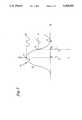
- FIG. 1is a perspective view of an IOC having an arrangement of optical modulators in accordance with the present invention
- FIG. 2is a graph of the transfer function of a Mach-Zehnder interferometer formed on a surface of the IOC of FIG. 1;
- FIG. 3is a block diagram of the IOC of FIG. 1 with additional apparatus in accordance with the present invention.
- FIG. 1is a perspective view of an IO chip 10 ("IOC") fabricated from a substrate 12 of, e.g., X-cut lithium niobate, LiNbO 3 , or lithium tantalate, LiTaO 3 .
- the IOC 10has a pair of series connected (i.e., "cascaded") optical waveguides 14,16 formed on a major surface 18 thereof.
- the waveguides 14,16may be formed in a number of well-known ways, including titanium indiffusion, proton exchange, or by an annealed proton exchange (“APETM”) process as disclosed and claimed in U.S. Pat. No. 4,984,861 to Suchoski Jr. et al., and assigned to the assignee of the present invention, and which is hereby incorporated by reference.
- APETMannealed proton exchange
- Each waveguide 14,16may be a Mach-Zehnder interferometer.
- an input optical signal 20comprising RF energy from, e.g., a laser light source 21 (FIG. 3) enters the Mach-Zehnder at an input port 22 and is split at a Y-junction 24 in the Mach-Zehnder into two equal components. Each component travels in a corresponding arm 26,28 before recombining at an output Y-junction 30.
- the recombined optical signaltravels in a section 32 of the waveguide to an input Y-junction 34 of the second Mach-Zehnder 16, where it is split into two equal components that traverse inside corresponding arms 36,38.
- the two light signalsrecombine at an output Y-junction 40 of the second Mach-Zehnder.
- the recombined signal 42represents the optical signal output of the waveguide.
- Each modulator 46,48comprises, e.g., two pairs of electrodes 52,54,56,58, one pair disposed on each side of an associated arm 26,28,36,38.
- the term "Mach-Zehnder”thus refers to the combination of the waveguide Y-junctions 24,30,34,40 and arms 26,28,36,38, along with the modulators 46,48.
- a time varying voltage, V wis fed as a traveling wave, or on a corresponding signal line 60, from an RF source 61 (FIG. 3) to electrode pairs 52,56.
- the RF sourceprovides the information to be modulated onto, and, thus, transmitted by, the carrier optical signal 20.
- the voltage V wproduces an electric field in the IOC substrate 12.
- the electric fieldeffectively changes the relative indices of refraction, and, thus, the optical path lengths of the waveguide arms 26,36. Modulation occurs since the relative phase of the optical signals at the corresponding output Y-junctions 30,40 vary according to the instantaneous amplitude of the time varying voltage V w .
- the varying phase relationship between the optical signals traversing in the waveguide armsresults in a varying amplitude of the intensity of the recombined optical signal 42 at the interferometer output.
- FIG. 2is a graph 70 of the transfer function of a typical electrooptic modulator.
- the transfer function 70is a nonlinear cosine curve 72.
- the abscissarepresents the voltage, V m , applied to the electrodes.
- V mis the total of any DC voltage plus the instantaneous amplitude of any time varying voltage, V w , applied to the electrodes.
- the ordinaterepresents optical power output, P o , of the Mach-Zehnder, as typically sensed by a detector (not shown).
- the input optical signal 20divides equally between the arms 26,28 in the first Mach-Zehnder 14. With zero voltage applied to the pair of electrodes 52, the optical signals recombine in phase with each other at the output Y-junction 30 of the first Mach-Zehnder 14. Thus, the optical signal at the first Mach-Zehnder output is essentially similar to the input optical signal 20. This phenomenon is described in more detail in U.S. Pat. No. 5,040,865 to Chen et al, which is hereby incorporated by reference.
- the optical signalpropagates to the input Y-junction 34 of the second Mach-Zehnder 16, where it is split into two equal components.
- the optical signalsWith zero voltage applied to the pair of electrodes 56, the optical signals recombine in phase with each other at the output Y-junction 40 of the second Mach-Zehnder 16 (assuming the signals were in phase at the input Y-junction 34 of the second Mach-Zehnder).
- the optical signal 42 at the output of the second Mach-Zehnderis essentially similar to the optical signal 20 input to the first Mach-Zehnder.
- the condition where zero voltage is applied to any modulatoris indicated at point A 74 on the graph 72 of FIG. 2.
- the graph of FIG. 2also illustrates the effect of applying a time varying voltage signal, V w , of angular frequency w to a modulator.
- V wtime varying voltage signal
- the Mach-Zehnder's output signalis also at frequency w.
- the Mach-Zehnder's output signalis now twice the modulation frequency; i.e., a fundamental frequency of 2 w. Also generated are harmonics of the fundamental frequency at even integral multiples; e.g., 4 w, 8 w, etc.
- modulator operation away from point Byields intermodulation harmonics. As described hereinbefore in regards to an exemplary CATV system, such harmonics are undesirable.
- FIG. 3is illustrated a block diagram of the apparatus of the present invention.
- the IOC 10 of FIG. 1is illustrated with two Mach-Zehnders 14,16 and corresponding modulators 52-58.
- the first Mach-Zehnder 14is configured to have a transfer function of:
- the second Mach-Zehnder 16is configured to have a transfer function of:
- the overall transfer function of the cascaded Mach-Zehnder pairis:
- the variable xrepresents the time varying voltage signal on the line 60 from the RF source 61.
- the variables ⁇ 1 and ⁇ 2represent phase offsets applied to the corresponding first and second modulators. Such modulator configuration and phase biases are accomplished by selectively biasing the modulators 54,58 with an appropriate DC voltage, as described hereinafter.
- the term kwhich has a value of less than one, is the contrast of the first modulator 46.
- the contrastis the ratio of amount of optical signal in arm 26 to the amount of optical signal in arm 28. The contrast may be adjusted by apportioning the amount of the input optical signal between the two arms 26,28 of the first modulator, using means described in detail hereinafter.
- k* ⁇ 2 *cos 2 (x)may be simplified as:
- the second and third order terms aboveare indicative of the second and third harmonics in the intermodulation distortion.
- the appropriate values for the contrast k and phase angles ⁇ 1 and ⁇ 2may be obtained.
- the inverse sin of 0.5yields an angle of 30°.
- kis set to -1/4.
- ⁇ 1is set to +15° and ⁇ 2 is set to -15°.
- the foregoing trigonometric expansionwas applied to a mathematical optimization software program, such as the commercially available Mathcad program. Such software optimization yielded a value of 0.92258/4 for the contrast k, and values of +/- 14.077° for ⁇ 1 and ⁇ 2 .
- the second and third harmonic terms of the trigonometric expansion of the composite transfer function in Eq. 3go to zero for specific values of contrast k, and phase adjustment ⁇ 1 and ⁇ 2.
- the third harmoniccan be significantly reduced.
- the second harmoniccan also be significantly reduced.
- a cutoff modulator 80is formed as a pair of electrodes 82 on the IOC major surface 18 in a similar manner to the optic modulators 46,48.
- the cutoff modulator 80apportions the amount of the optical input signal 20 between the two arms 26,28 of the first Mach-Zehnder 14 to set the contrast k.
- the modulatoris fabricated, e.g., in the vicinity of one arm 28 of the first Mach-Zehnder.
- the cutoff modulator 80may instead be fabricated in conjunction with the second Mach-Zehnder 16, without departing from the broadest scope of the present invention.
- the accuracy of kis not strict. For example, to achieve a 20 dB reduction in the third harmonic, k must be set to an accuracy of 10%.
- Other optical meansmay be employed, besides the cutoff modulator so described, to apportion the light between the two arms.
- the amount of contrastis controlled by a contrast control circuit 84 which provides a signal on a line 86 to the cutoff modulator 80.
- the contrast circuitis responsive to a pair of electrical signals: a first signal on a line 88 indicative of the average DC voltage value of the optical output signal 42 from the second Mach-Zehnder; a second signal on a line 90 indicative of the average DC voltage value of the first harmonic of the optical output signal 42.
- the contrast circuit 84compares these two signals 88,90 and adjusts the contrast accordingly.
- the contrast control circuitmay comprise a commonly available analog multiplier configured as a divider.
- the optical signal 42 at the output of the second Mach-Zehnder 16is provided to each of a pair of known synchronous demodulator or lock-in amplifier circuits 92,94.
- the circuits 92,94may be the Model AD640 DC Coupled Demodulating Amplifier provided by Analog Devices.
- the first demodulator 92demodulates the first harmonic from the optical output of the second Mach-Zehnder.
- the circuit 92provides the DC voltage signal indicative of the average DC voltage value of the first harmonic on the line 90 to the contrast circuit 84.
- the second demodulator 94demodulates the second harmonic from the output of the second Mach-Zehnder.
- the signal lineis fed to one input of a second summer 98.
- the second demodulatoralso provides a dither signal on a line 100 to an input of each of the first and second summers 95,98.
- the summerssum the dither signal with the corresponding DC voltage signal on the lines 93,96 and provide the summed signals on lines 102,104 to the respective modulators 54,58.
- the dither signalis at a frequency equal to the second harmonic of the optical signal 42 at the output of the second Mach-Zehnder 16. Biasing the modulators 54,58 with a dither signal at the frequency of the second harmonic controls the bias point of each modulator for reduction of the third harmonic.
- the cascaded modulator arrangementachieved as much as a 35 dB improvement in reduction in the third order harmonic, as compared to a normal Mach-Zehnder.
- the first modulatorcreates a DC multiplier for the modulation products of the second modulator, and generates a controlled magnitude second harmonic whose product with the sin(x) term, in the second modulator creates a new third harmonic which cancels out the third harmonic generated by the sin(x) term in the second stage.
- Phase offset of the two modulatorsis then adjusted to null out any resulting second harmonic from the two modulators.
- a controlled contrast term, kis used to apply the correction term.
- the input RF modulationneed only have a bandwidth consistent with the information bandwidth, and not a bandwidth three times as great, as would be needed for the aforedescribed predistortion schemes in the prior art.
- the composite device bandwidthscan be as great as the optic modulator itself provides.
- traveling wave optic modulatorsmay be arranged in cascade with attention paid to propagation delays that would allow linearization out into the microwave spectrum
- the cascaded optic modulator arrangement of the present inventionhas an advantage over prior art parallel optic schemes in that splitting losses are avoided by passing the optical signal through a single path. Further, a single source is used, and the source wavelength can be as pure as needed. This is not possible in schemes employing incoherent summing of the correction term. Still further, the third order harmonic is trigonometrically added in the optical domain; thus, in no way limiting any electronics either on the transmit or receive end.
- the inventionhas been described with Mach-Zehnder interferometers fabricated on a surface of the IOC. However, it is to be understood that other types of interferometers, such as Balanced Bridge, may be used in light of the teachings herein without departing from the spirit and scope of the present invention. Further, the invention has been described as being fabricated on an integrated optical device. The invention may, if desired, be practiced instead with an all-fiber type of system using commercially available discrete interferometric and modulation devices.
- contrast control circuit 84the demodulators 92,94 and the summers 95,98 described herein are purely exemplary; other means for adjusting the contrast of the RF energy in one interferometer and for biasing the modulators 54,58 may be utilized, if desired, in light of the teachings herein and their use should be apparent to one of ordinary skill in the art. It suffice for the present invention that the phase offset of both modulators, and contrast of one modulator, are adjusted to minimize both second and third order harmonics inherently generated by the modulation process of each modulator, thereby providing an improved linear response in the optical signal at the output of the second Mach-Zehnder.
Landscapes
- Physics & Mathematics (AREA)
- Nonlinear Science (AREA)
- General Physics & Mathematics (AREA)
- Optics & Photonics (AREA)
- Engineering & Computer Science (AREA)
- Microelectronics & Electronic Packaging (AREA)
- Optical Modulation, Optical Deflection, Nonlinear Optics, Optical Demodulation, Optical Logic Elements (AREA)
Abstract
Description
1+k*cos(x) (Eq. 1)
1+Φ.sub.1 *sin(x)+Φ.sub.2 *cos(x) (Eq. 2)
(1+k*cos(x))*(1+Φ.sub.1 *sin(x)+Φ.sub.2 *cos(x)) (Eq. 3)
1+k*cos(x)+Φ.sub.1 *sin(x)+k*Φ.sub.1 *cos(x)*sin(x)+Φ.sub.2 *cos(x)+k*Φ.sub.2 *cos.sup.2 (x) (Eq. 4)
1/2*k*Φ.sub.1 *sin(2x) (Eq. 5)
1/2*k*Φ.sub.2 *(1+cos(2x)) (Eq. 6)
1+k*cos(x)+Φ.sub.1 *sin(x)+1/2*k*Φ.sub.1 *sin(2x)+Φ.sub.2 *cos(x)+1/2*k*Φ.sub.2 +1/2*k*Φ.sub.2 *cos(2x)) (Eq. 7)
Φ.sub.1 *sin(x)=Φ.sub.1 [x-1/6*x.sup.3 +1/120*x.sup.5 - . . . ](Eq. 8)
(k+Φ.sub.2)(cos(x))=(k+Φ.sub.2)[1-1/2*x.sup.2 +1/24*x.sup.4 - . . . ] (Eq. 9)
(1/2*k*Φ.sub.1)(sin(2x ))=(1/2*k*Φ.sub.1)[2x-8/6*x.sup.3 +32/120*x.sup.5 + . . . ] (Eq. 10)
(1/2*k*Φ.sub.2)cos(2x)=(1/2*k*Φ.sub.2)[1-2x.sup.2 +2/3*x.sup.4 - . . . ] (Eq. 11)
DC: 1+(1/2*k*Φ.sub.2)+(k+Φ.sub.2)+(1/2*k*Φ.sub.2) (Eq. 12)
x: Φ.sub.1 +k*Φ.sub.1 =Φ.sub.1 (1+k) (Eq. 13)
x.sup.2 : -(1/2*k*Φ.sub.2)-k*Φ.sub.2 =-k/2-Φ.sub.2 /2-k*Φ.sub.2 (Eq. 14)
x.sup.3 : -Φ.sub.1 /6-(1/2*k*Φ.sub.1)(8/6)=-1/6(Φ.sub.1 +4*k*Φ.sub.1)=-1/6*Φ.sub.1 (1+4*k) (Eq. 15)
x.sup.4 : (k+Φ.sub.2)/24+(k+Φ.sub.2)/3=k/24+Φ.sub.2 /24+(k*Φ.sub.2)/3 (Eq. 16)
x.sup.5 : Φ.sub.1 /120+(1/2*k*Φ.sub.1)(32/120)=Φ.sub.1 (1/120+k*16/120) =Φ.sub.1 /120(1+16*k) (Eq. 17)
Claims (20)
Priority Applications (1)
| Application Number | Priority Date | Filing Date | Title |
|---|---|---|---|
| US07/803,818US5168534A (en) | 1991-12-09 | 1991-12-09 | Cascaded optic modulator arrangement |
Applications Claiming Priority (1)
| Application Number | Priority Date | Filing Date | Title |
|---|---|---|---|
| US07/803,818US5168534A (en) | 1991-12-09 | 1991-12-09 | Cascaded optic modulator arrangement |
Publications (1)
| Publication Number | Publication Date |
|---|---|
| US5168534Atrue US5168534A (en) | 1992-12-01 |
Family
ID=25187513
Family Applications (1)
| Application Number | Title | Priority Date | Filing Date |
|---|---|---|---|
| US07/803,818Expired - LifetimeUS5168534A (en) | 1991-12-09 | 1991-12-09 | Cascaded optic modulator arrangement |
Country Status (1)
| Country | Link |
|---|---|
| US (1) | US5168534A (en) |
Cited By (50)
| Publication number | Priority date | Publication date | Assignee | Title |
|---|---|---|---|---|
| US5237629A (en)* | 1992-03-19 | 1993-08-17 | The United States Of America As Represented By The United States Department Of Energy | Digitally controlled distributed phase shifter |
| US5278923A (en)* | 1992-09-02 | 1994-01-11 | Harmonic Lightwaves, Inc. | Cascaded optical modulation system with high linearity |
| US5400417A (en)* | 1993-06-01 | 1995-03-21 | United Technologies Corporation | Electro-optic modulator having gated-dither bias control |
| US5416858A (en)* | 1991-06-27 | 1995-05-16 | Thomson-Csf | Integrated electrooptical modulation device |
| US5422966A (en)* | 1994-06-10 | 1995-06-06 | Gopalakrishnan; Ganesh K. | Microwave electro-optic mixer |
| US5467414A (en)* | 1992-09-16 | 1995-11-14 | Deutache Aerospace Ag | Device for generating feedback signals to regulate optical monitoring circuits (PLL) |
| US5532867A (en)* | 1995-06-06 | 1996-07-02 | Hughes Aircraft Company | Bias stabilization circuit and method for a linearized directional coupler modulator |
| US5615037A (en)* | 1995-01-17 | 1997-03-25 | Massachusetts Institute Of Technology | Sub-octave bandpass optical remote antenna link modulator and method therefor |
| US5644665A (en)* | 1995-07-27 | 1997-07-01 | The United States Of America As Represented By The Secretary Of The Navy | Multi-octave, high dynamic range operation of low-biased modulators by balanced detection |
| US5710653A (en)* | 1995-03-06 | 1998-01-20 | Fiber Optic Network Solutions Corp. | Linear multi-output optical transmitter system |
| US5757985A (en)* | 1994-11-16 | 1998-05-26 | Nec Corporation | Semiconductor mach-zehnder-type optical modulator |
| US5781327A (en)* | 1996-08-19 | 1998-07-14 | Trw Inc. | Optically efficient high dynamic range electro-optic modulator |
| US5875048A (en)* | 1995-03-06 | 1999-02-23 | Cfx Communication Systems,Llc | Linear multi-output optical transmitter system |
| US5915052A (en)* | 1997-06-30 | 1999-06-22 | Uniphase Telecommunications Products, Inc. | Loop status monitor for determining the amplitude of the signal components of a multi-wavelength optical beam |
| US5953139A (en)* | 1996-03-06 | 1999-09-14 | Cfx Communications Systems, Llc | Wavelength division multiplexing system |
| US5982964A (en)* | 1997-06-30 | 1999-11-09 | Uniphase Corporation | Process for fabrication and independent tuning of multiple integrated optical directional couplers on a single substrate |
| US6020986A (en)* | 1997-11-21 | 2000-02-01 | Jds Uniphase Corporation | Programmable add-drop module for use in an optical circuit |
| US6031849A (en)* | 1997-11-14 | 2000-02-29 | Jds Uniphase Corporation | High power three level fiber laser and method of making same |
| US6091864A (en)* | 1997-04-10 | 2000-07-18 | Ortel Corporation | Linear optical modulator for providing chirp-free optical signals |
| US6151157A (en)* | 1997-06-30 | 2000-11-21 | Uniphase Telecommunications Products, Inc. | Dynamic optical amplifier |
| EP0950167A4 (en)* | 1996-10-18 | 2001-02-07 | Uniphase Corp | Variable chirp optical modulator using single modulation source |
| US6192167B1 (en)* | 1998-07-24 | 2001-02-20 | Uniphase Telecommunications Products | Differential drive optical modulator |
| US6226424B1 (en) | 1997-09-19 | 2001-05-01 | Uniphase Telecommunications Products, Inc. | Integrated wavelength-select transmitter |
| US6341184B1 (en)* | 1999-09-10 | 2002-01-22 | Nannovation Technologies, Inc. | Low drive voltage optical modulator |
| US6407846B1 (en) | 2001-03-16 | 2002-06-18 | All Optical Networks, Inc. | Photonic wavelength shifting method |
| US6483954B2 (en)* | 2000-12-20 | 2002-11-19 | Intel Corporation | Method and apparatus for coupling to regions in an optical modulator |
| US20030026199A1 (en)* | 2001-08-03 | 2003-02-06 | Myers Michael H. | Code-division, minimum-shift-keying optical multiplexing |
| WO2003012535A1 (en)* | 2001-07-27 | 2003-02-13 | Axe, Inc. | Optical pulse generator with single frequency drive |
| US6529647B2 (en)* | 2000-03-14 | 2003-03-04 | Fujitsu Limited | Optical device with optical waveguides and manufacturing method therefor |
| US20030053178A1 (en)* | 2001-08-28 | 2003-03-20 | Karlquist Richard K. | Frequency translating devices and frequency translating measurement systems that utilize light-activated resistors |
| JP3404604B2 (en) | 1994-04-28 | 2003-05-12 | エヌイーシートーキン株式会社 | Optical electric field sensor |
| US6567203B1 (en) | 2001-02-23 | 2003-05-20 | Big Bear Networks, Inc. | Tri-electrode traveling wave optical modulators and methods |
| US6587256B2 (en)* | 2001-06-06 | 2003-07-01 | Northrop Grumman Corporation | RF combiner based on cascaded optical phase modulation |
| US20030147591A1 (en)* | 2002-02-07 | 2003-08-07 | Fujitsu Limited | Optical waveguide device and optical modulator |
| US20040008395A1 (en)* | 2000-11-22 | 2004-01-15 | Jds Uniphase Corporation | Cascaded RZ and NRZ laser modulators having RZ/NRZ phase alignment bias control |
| US6738174B1 (en) | 2001-02-23 | 2004-05-18 | Big Bear Networks, Inc. | Dual-electrode traveling wave optical modulators and methods |
| US20040240765A1 (en)* | 2003-05-30 | 2004-12-02 | Jds Uniphase Corporation | Optical digital external modulator |
| US7095543B1 (en) | 2001-02-23 | 2006-08-22 | Finisar Corporation | Dual-electrode traveling wave optical phase shifters and methods |
| US20070019896A1 (en)* | 2005-07-25 | 2007-01-25 | Darcie Thomas E | Class-AB microwave-photonic link |
| US20070041735A1 (en)* | 2005-08-22 | 2007-02-22 | Darcie Thomas E | Photonic link using angle modulation and method of use thereof |
| US7212326B2 (en) | 2003-05-30 | 2007-05-01 | Jds Uniphase Corporation | Optical external modulator |
| US20090009259A1 (en)* | 2006-01-13 | 2009-01-08 | Tomoaki Ohira | Angle modulator |
| US20090214151A1 (en)* | 2006-04-26 | 2009-08-27 | Georgia Tech Research Corporation | High Speed Optical Switch |
| US20120294608A1 (en)* | 2011-05-20 | 2012-11-22 | The Trustees Of Princeton University | System and method for broadband rf interference cancellation |
| US20130195394A1 (en)* | 2012-01-31 | 2013-08-01 | National Institute Of Information And Communications Technology | Optical modulator |
| EP2090927A4 (en)* | 2006-09-06 | 2014-12-17 | Nat Inst Inf & Comm Tech | METHOD AND DEVICE FOR GENERATING A QUICK MULTIPLYED SIGNAL |
| CN108173596A (en)* | 2012-08-23 | 2018-06-15 | 菲尼萨公司 | For the integration laser and modulator transmitter of CATV applications |
| WO2021050599A1 (en)* | 2019-09-10 | 2021-03-18 | HyperLight Corporation | Integrated electro-optic frequency comb generator |
| US20210223657A1 (en)* | 2018-04-30 | 2021-07-22 | President And Fellows Of Harvard College | Active photonic networks on integrated lithium niobate platforms |
| US20210391694A1 (en)* | 2018-12-25 | 2021-12-16 | Mitsubishi Electric Corporation | Optical transmission apparatus |
Citations (1)
| Publication number | Priority date | Publication date | Assignee | Title |
|---|---|---|---|---|
| US5101450A (en)* | 1991-01-23 | 1992-03-31 | Gte Laboratories Incorporated | Quadrature optical phase modulators for lightwave systems |
- 1991
- 1991-12-09USUS07/803,818patent/US5168534A/ennot_activeExpired - Lifetime
Patent Citations (1)
| Publication number | Priority date | Publication date | Assignee | Title |
|---|---|---|---|---|
| US5101450A (en)* | 1991-01-23 | 1992-03-31 | Gte Laboratories Incorporated | Quadrature optical phase modulators for lightwave systems |
Non-Patent Citations (22)
| Title |
|---|
| Bodeep, G. E. et al., "Comparison of Second- and Third-Order Distortion in Intensity Modulated InGaAsP Lasers and a LiNbO3 External Modulator", OFC '89, paper WK-2. |
| Bodeep, G. E. et al., Comparison of Second and Third Order Distortion in Intensity Modulated InGaAsP Lasers and a LiNbO 3 External Modulator , OFC 89, paper WK 2.* |
| Childs, R. B. et al., "Predistortion Linearization of Directly Modulated DFB Lasers and External Modulators for AM Radio Transmission", Technical Digest, Optical Fiber Communication Conf., Optical Society of America, Wash., D.C., 1990, paper WH-6. |
| Childs, R. B. et al., Predistortion Linearization of Directly Modulated DFB Lasers and External Modulators for AM Radio Transmission , Technical Digest, Optical Fiber Communication Conf., Optical Society of America, Wash., D.C., 1990, paper WH 6.* |
| DeRidder, R. M. et al., "Feedforward Compensation of Integrated Optic Modulator Distortion", paper WH-5. |
| DeRidder, R. M. et al., Feedforward Compensation of Integrated Optic Modulator Distortion , paper WH 5.* |
| Donaldson, A. et al., "Linearity Considerations in High Performance Amplitude Modulators", IEE Colloquim on `Analogue Optical Communications`, Digest No. 156, Dec. 1989, pp. 4/1-5. |
| Donaldson, A. et al., Linearity Considerations in High Performance Amplitude Modulators , IEE Colloquim on Analogue Optical Communications , Digest No. 156, Dec. 1989, pp. 4/1 5.* |
| Farwell, Mark et al., "An Electrooptic Intensity Modulator with Improved Linearity", IEEE Photonics Technology Letters, 1991, vol. 3, No. 9, pp. 792-795. |
| Farwell, Mark et al., An Electrooptic Intensity Modulator with Improved Linearity , IEEE Photonics Technology Letters, 1991, vol. 3, No. 9, pp. 792 795.* |
| Lin, Z. Q. et al., Reduction of Intermodulation Distortion of Interferometric Optical Modulators Through Incoherent Mixing of Optical Waves , Electronics Letters, 1990, vol. 26, No. 23, pp. 1980 1982.* |
| Lin, Z. Q. et al., Waveguide Modulators with Extended Linear Dynamic Range a Theoretical Prediction , IEEE Photonics Technology Letters, vol. 2, No. 12, Dec. 1990, pp. 884 886.* |
| Lin, Z.-Q. et al., "Reduction of Intermodulation Distortion of Interferometric Optical Modulators Through Incoherent Mixing of Optical Waves", Electronics Letters, 1990, vol. 26, No. 23, pp. 1980-1982. |
| Lin, Z.-Q. et al., "Waveguide Modulators with Extended Linear Dynamic Range-a Theoretical Prediction", IEEE Photonics Technology Letters, vol. 2, No. 12, Dec. 1990, pp. 884-886. |
| Liu, P. L. et al., In Search of a Linear Electrooptic Amplitude Modulator , IEEE Photonics Technology Letters, vol. 3, No. 2, Feb. 1991, pp. 144 146.* |
| Liu, P.-L. et al., "In Search of a Linear Electrooptic Amplitude Modulator", IEEE Photonics Technology Letters, vol. 3, No. 2, Feb. 1991, pp. 144-146. |
| Suto, Ko ichi, et al., Intermodulation Distortion in 48 TV Channel FM FDM Optical Transmission , IEEE Photonics Technology Letters, 1991, vol. 3, No. 9, pp. 844 846.* |
| Suto, Ko-ichi, et al., "Intermodulation Distortion in 48 TV Channel FM-FDM Optical Transmission", IEEE Photonics Technology Letters, 1991, vol. 3, No. 9, pp. 844-846. |
| Wu, Jingshown et al., "Linearization of Laser-Diode Nonlinearity of Broadband Analogue Fiber-Optic Communication", International Journal of Optoelectronics, 1988, vol. 3, No. 6, pp. 523-533. |
| Wu, Jingshown et al., Linearization of Laser Diode Nonlinearity of Broadband Analogue Fiber Optic Communication , International Journal of Optoelectronics, 1988, vol. 3, No. 6, pp. 523 533.* |
| Zolotov, E. M., et al., "Integrated Optical Mach-Zehnder Modulator with a Linearized Modulation Characteristic", Sov. J. Quantum Electron, 18(3) 1988, pp. 401-402. |
| Zolotov, E. M., et al., Integrated Optical Mach Zehnder Modulator with a Linearized Modulation Characteristic , Sov. J. Quantum Electron, 18(3) 1988, pp. 401 402.* |
Cited By (66)
| Publication number | Priority date | Publication date | Assignee | Title |
|---|---|---|---|---|
| US5416858A (en)* | 1991-06-27 | 1995-05-16 | Thomson-Csf | Integrated electrooptical modulation device |
| US5237629A (en)* | 1992-03-19 | 1993-08-17 | The United States Of America As Represented By The United States Department Of Energy | Digitally controlled distributed phase shifter |
| US5278923A (en)* | 1992-09-02 | 1994-01-11 | Harmonic Lightwaves, Inc. | Cascaded optical modulation system with high linearity |
| WO1994006042A1 (en)* | 1992-09-02 | 1994-03-17 | Harmonic Lightwaves, Inc. | Cascaded optical modulation system with high linearity |
| US5467414A (en)* | 1992-09-16 | 1995-11-14 | Deutache Aerospace Ag | Device for generating feedback signals to regulate optical monitoring circuits (PLL) |
| US5400417A (en)* | 1993-06-01 | 1995-03-21 | United Technologies Corporation | Electro-optic modulator having gated-dither bias control |
| JP3404604B2 (en) | 1994-04-28 | 2003-05-12 | エヌイーシートーキン株式会社 | Optical electric field sensor |
| US5422966A (en)* | 1994-06-10 | 1995-06-06 | Gopalakrishnan; Ganesh K. | Microwave electro-optic mixer |
| US5757985A (en)* | 1994-11-16 | 1998-05-26 | Nec Corporation | Semiconductor mach-zehnder-type optical modulator |
| US5615037A (en)* | 1995-01-17 | 1997-03-25 | Massachusetts Institute Of Technology | Sub-octave bandpass optical remote antenna link modulator and method therefor |
| US5867295A (en)* | 1995-01-17 | 1999-02-02 | Massachusetts Institute Of Technology | Sub-octave bandpass optical remote antenna link modulator and method therefor |
| US5710653A (en)* | 1995-03-06 | 1998-01-20 | Fiber Optic Network Solutions Corp. | Linear multi-output optical transmitter system |
| US5875048A (en)* | 1995-03-06 | 1999-02-23 | Cfx Communication Systems,Llc | Linear multi-output optical transmitter system |
| US6163395A (en)* | 1995-03-06 | 2000-12-19 | Fiber Optics Network Solutions Corp. | Linear multi-output optical transmitter system |
| US5532867A (en)* | 1995-06-06 | 1996-07-02 | Hughes Aircraft Company | Bias stabilization circuit and method for a linearized directional coupler modulator |
| US5644665A (en)* | 1995-07-27 | 1997-07-01 | The United States Of America As Represented By The Secretary Of The Navy | Multi-octave, high dynamic range operation of low-biased modulators by balanced detection |
| US5953139A (en)* | 1996-03-06 | 1999-09-14 | Cfx Communications Systems, Llc | Wavelength division multiplexing system |
| US5781327A (en)* | 1996-08-19 | 1998-07-14 | Trw Inc. | Optically efficient high dynamic range electro-optic modulator |
| JP3433753B2 (en) | 1996-10-18 | 2003-08-04 | ユニフェース テレコミュニケーションズ プロダクツ インコーポレイテッド | Tunable chirped light modulator using a single modulation source |
| EP0950167A4 (en)* | 1996-10-18 | 2001-02-07 | Uniphase Corp | Variable chirp optical modulator using single modulation source |
| US6091864A (en)* | 1997-04-10 | 2000-07-18 | Ortel Corporation | Linear optical modulator for providing chirp-free optical signals |
| US5982964A (en)* | 1997-06-30 | 1999-11-09 | Uniphase Corporation | Process for fabrication and independent tuning of multiple integrated optical directional couplers on a single substrate |
| US6151157A (en)* | 1997-06-30 | 2000-11-21 | Uniphase Telecommunications Products, Inc. | Dynamic optical amplifier |
| US5915052A (en)* | 1997-06-30 | 1999-06-22 | Uniphase Telecommunications Products, Inc. | Loop status monitor for determining the amplitude of the signal components of a multi-wavelength optical beam |
| US6370290B1 (en) | 1997-09-19 | 2002-04-09 | Uniphase Corporation | Integrated wavelength-select transmitter |
| US6226424B1 (en) | 1997-09-19 | 2001-05-01 | Uniphase Telecommunications Products, Inc. | Integrated wavelength-select transmitter |
| US6031849A (en)* | 1997-11-14 | 2000-02-29 | Jds Uniphase Corporation | High power three level fiber laser and method of making same |
| US6020986A (en)* | 1997-11-21 | 2000-02-01 | Jds Uniphase Corporation | Programmable add-drop module for use in an optical circuit |
| US6192167B1 (en)* | 1998-07-24 | 2001-02-20 | Uniphase Telecommunications Products | Differential drive optical modulator |
| US6341184B1 (en)* | 1999-09-10 | 2002-01-22 | Nannovation Technologies, Inc. | Low drive voltage optical modulator |
| US6529647B2 (en)* | 2000-03-14 | 2003-03-04 | Fujitsu Limited | Optical device with optical waveguides and manufacturing method therefor |
| US6917455B2 (en) | 2000-11-22 | 2005-07-12 | Jds Uniphase Corporation | Cascaded RZ and NRZ laser modulators having RZ/NRZ phase alignment bias control |
| US20040008395A1 (en)* | 2000-11-22 | 2004-01-15 | Jds Uniphase Corporation | Cascaded RZ and NRZ laser modulators having RZ/NRZ phase alignment bias control |
| US6483954B2 (en)* | 2000-12-20 | 2002-11-19 | Intel Corporation | Method and apparatus for coupling to regions in an optical modulator |
| US7095543B1 (en) | 2001-02-23 | 2006-08-22 | Finisar Corporation | Dual-electrode traveling wave optical phase shifters and methods |
| US6567203B1 (en) | 2001-02-23 | 2003-05-20 | Big Bear Networks, Inc. | Tri-electrode traveling wave optical modulators and methods |
| US6738174B1 (en) | 2001-02-23 | 2004-05-18 | Big Bear Networks, Inc. | Dual-electrode traveling wave optical modulators and methods |
| US6407846B1 (en) | 2001-03-16 | 2002-06-18 | All Optical Networks, Inc. | Photonic wavelength shifting method |
| US6587256B2 (en)* | 2001-06-06 | 2003-07-01 | Northrop Grumman Corporation | RF combiner based on cascaded optical phase modulation |
| WO2003012535A1 (en)* | 2001-07-27 | 2003-02-13 | Axe, Inc. | Optical pulse generator with single frequency drive |
| US20030026199A1 (en)* | 2001-08-03 | 2003-02-06 | Myers Michael H. | Code-division, minimum-shift-keying optical multiplexing |
| US20030053178A1 (en)* | 2001-08-28 | 2003-03-20 | Karlquist Richard K. | Frequency translating devices and frequency translating measurement systems that utilize light-activated resistors |
| US20030147591A1 (en)* | 2002-02-07 | 2003-08-07 | Fujitsu Limited | Optical waveguide device and optical modulator |
| US7340114B2 (en)* | 2002-02-07 | 2008-03-04 | Fujitsu Limited | Optical waveguide device and optical modulator |
| US20040240765A1 (en)* | 2003-05-30 | 2004-12-02 | Jds Uniphase Corporation | Optical digital external modulator |
| US6961166B2 (en) | 2003-05-30 | 2005-11-01 | Jds Uniphase Corporation | Optical digital external modulator |
| US7212326B2 (en) | 2003-05-30 | 2007-05-01 | Jds Uniphase Corporation | Optical external modulator |
| US20070019896A1 (en)* | 2005-07-25 | 2007-01-25 | Darcie Thomas E | Class-AB microwave-photonic link |
| US7359580B2 (en)* | 2005-07-25 | 2008-04-15 | University Of Victoria Innovation And Development Corporation | Class-AB microwave-photonic link |
| US20070041735A1 (en)* | 2005-08-22 | 2007-02-22 | Darcie Thomas E | Photonic link using angle modulation and method of use thereof |
| US7369715B2 (en) | 2005-08-22 | 2008-05-06 | University Of Victoria Innovation And Development Corporation | Photonic link using angle modulation and method of use thereof |
| US20090009259A1 (en)* | 2006-01-13 | 2009-01-08 | Tomoaki Ohira | Angle modulator |
| US20090214151A1 (en)* | 2006-04-26 | 2009-08-27 | Georgia Tech Research Corporation | High Speed Optical Switch |
| EP2090927A4 (en)* | 2006-09-06 | 2014-12-17 | Nat Inst Inf & Comm Tech | METHOD AND DEVICE FOR GENERATING A QUICK MULTIPLYED SIGNAL |
| US8682170B2 (en)* | 2011-05-20 | 2014-03-25 | The Trustees Of Princeton University | System and method for broadband RF interference cancellation |
| US20120294608A1 (en)* | 2011-05-20 | 2012-11-22 | The Trustees Of Princeton University | System and method for broadband rf interference cancellation |
| US20130195394A1 (en)* | 2012-01-31 | 2013-08-01 | National Institute Of Information And Communications Technology | Optical modulator |
| US9250455B2 (en)* | 2012-01-31 | 2016-02-02 | Sumitomo Osaka Cement Co., Ltd. | Optical modulator |
| CN108173596A (en)* | 2012-08-23 | 2018-06-15 | 菲尼萨公司 | For the integration laser and modulator transmitter of CATV applications |
| US20210223657A1 (en)* | 2018-04-30 | 2021-07-22 | President And Fellows Of Harvard College | Active photonic networks on integrated lithium niobate platforms |
| US12015247B2 (en)* | 2018-12-25 | 2024-06-18 | Mitsubishi Electric Corporation | Optical transmission apparatus |
| US20210391694A1 (en)* | 2018-12-25 | 2021-12-16 | Mitsubishi Electric Corporation | Optical transmission apparatus |
| WO2021050599A1 (en)* | 2019-09-10 | 2021-03-18 | HyperLight Corporation | Integrated electro-optic frequency comb generator |
| US11733586B2 (en) | 2019-09-10 | 2023-08-22 | HyperLight Corporation | Integrated electro-optic frequency comb generator |
| US11307484B2 (en) | 2019-09-10 | 2022-04-19 | HyperLight Corporation | Integrated electro-optic frequency comb generator |
| US12253786B2 (en) | 2019-09-10 | 2025-03-18 | HyperLight Corporation | Integrated electro-optic frequency comb generator |
Similar Documents
| Publication | Publication Date | Title |
|---|---|---|
| US5168534A (en) | Cascaded optic modulator arrangement | |
| EP0612452B1 (en) | Apparatus for linearization of optic modulators using a feed-forward predistortion circuit | |
| US5321543A (en) | Apparatus and method for linearizing an external optical modulator | |
| US6091864A (en) | Linear optical modulator for providing chirp-free optical signals | |
| EP0484791B1 (en) | Apparatus and method for externally modulating an optical carrier | |
| US4288785A (en) | Light intensity modulator with digital control and a digital-analog converter comprising such a modulator | |
| US5532857A (en) | Wide dynamic range optical link using DSSC linearizer | |
| US5109441A (en) | Fiber optic external modulator | |
| US5031235A (en) | Cable system incorporating highly linear optical modulator | |
| US6532315B1 (en) | Variable chirp optical modulator having different length electrodes | |
| US5148503A (en) | Apparatus and method for linearized cascade coupled integrated optical modulator | |
| EP0950167B1 (en) | Variable chirp optical modulator using single modulation source | |
| US5708734A (en) | Polarisation-independent optical device | |
| US5040865A (en) | Frequency multiplying electro-optic modulator configuration and method | |
| EP0407919B1 (en) | Optical transmitters linearized by means of parametric feedback | |
| US5323406A (en) | Photonic mixer for photonically multiplying two electrical signals in two optically interconnected interferometric modulators operated at modulation outside the linear range | |
| CA2200236C (en) | High-speed polarization scrambler with adjustable chirp | |
| US5309532A (en) | Electro-optic intensity modulator with improved linearity | |
| US5002353A (en) | Apparatus and method for reducing modulator nonlinearities | |
| US6239897B1 (en) | Chirp-controlled optical modulator and method of controlling chirp in the modulation of an optical signal | |
| US5230028A (en) | Electro-optic intensity modulator with improved linearity | |
| US6996345B1 (en) | Linearization of intensity modulators using quadratic electro-optic effect | |
| US5126870A (en) | Linear broadband signal generator using primary and secondary optical modulators | |
| US6535653B1 (en) | Variable chirp optical modulator | |
| WO2006037181A1 (en) | An optical signal processing device |
Legal Events
| Date | Code | Title | Description |
|---|---|---|---|
| AS | Assignment | Owner name:UNITED TECHNOLOGIES CORPORATION, CONNECTICUT Free format text:ASSIGNMENT OF ASSIGNORS INTEREST.;ASSIGNORS:MCBRIEN, GREGORY J.;FARINA, JAMES D.;REEL/FRAME:005948/0970 Effective date:19911204 | |
| STCF | Information on status: patent grant | Free format text:PATENTED CASE | |
| CC | Certificate of correction | ||
| FEPP | Fee payment procedure | Free format text:PAYOR NUMBER ASSIGNED (ORIGINAL EVENT CODE: ASPN); ENTITY STATUS OF PATENT OWNER: LARGE ENTITY | |
| FPAY | Fee payment | Year of fee payment:4 | |
| SULP | Surcharge for late payment | ||
| REMI | Maintenance fee reminder mailed | ||
| AS | Assignment | Owner name:UNIPHASE TELECOMMUNICATIONS PRODUCTS, INC., CONNEC Free format text:ASSIGNMENT OF ASSIGNORS INTEREST;ASSIGNOR:UNITED TECHNOLOGIES CORPORATION;REEL/FRAME:008792/0265 Effective date:19950505 | |
| FEPP | Fee payment procedure | Free format text:PAYER NUMBER DE-ASSIGNED (ORIGINAL EVENT CODE: RMPN); ENTITY STATUS OF PATENT OWNER: LARGE ENTITY | |
| FPAY | Fee payment | Year of fee payment:8 | |
| AS | Assignment | Owner name:JDS UNIPHASE CORPORATION, CALIFORNIA Free format text:ASSIGNMENT OF ASSIGNORS INTEREST;ASSIGNOR:UNIPHASE TELECOMMUNICATIONS PRODUCTS, INC.;REEL/FRAME:013295/0189 Effective date:20020815 | |
| FPAY | Fee payment | Year of fee payment:12 | |
| FEPP | Fee payment procedure | Free format text:PAYOR NUMBER ASSIGNED (ORIGINAL EVENT CODE: ASPN); ENTITY STATUS OF PATENT OWNER: LARGE ENTITY |