US5168078A - Method of making high density semiconductor structure - Google Patents
Method of making high density semiconductor structureDownload PDFInfo
- Publication number
- US5168078A US5168078AUS07/631,671US63167190AUS5168078AUS 5168078 AUS5168078 AUS 5168078AUS 63167190 AUS63167190 AUS 63167190AUS 5168078 AUS5168078 AUS 5168078A
- Authority
- US
- United States
- Prior art keywords
- forming
- metal layers
- semiconductor substrate
- substrate
- metal
- Prior art date
- Legal status (The legal status is an assumption and is not a legal conclusion. Google has not performed a legal analysis and makes no representation as to the accuracy of the status listed.)
- Expired - Fee Related
Links
Images

Classifications
- H—ELECTRICITY
- H01—ELECTRIC ELEMENTS
- H01L—SEMICONDUCTOR DEVICES NOT COVERED BY CLASS H10
- H01L23/00—Details of semiconductor or other solid state devices
- H01L23/52—Arrangements for conducting electric current within the device in operation from one component to another, i.e. interconnections, e.g. wires, lead frames
- H01L23/535—Arrangements for conducting electric current within the device in operation from one component to another, i.e. interconnections, e.g. wires, lead frames including internal interconnections, e.g. cross-under constructions
- H—ELECTRICITY
- H01—ELECTRIC ELEMENTS
- H01L—SEMICONDUCTOR DEVICES NOT COVERED BY CLASS H10
- H01L23/00—Details of semiconductor or other solid state devices
- H01L23/48—Arrangements for conducting electric current to or from the solid state body in operation, e.g. leads, terminal arrangements ; Selection of materials therefor
- H01L23/481—Internal lead connections, e.g. via connections, feedthrough structures
- H—ELECTRICITY
- H01—ELECTRIC ELEMENTS
- H01L—SEMICONDUCTOR DEVICES NOT COVERED BY CLASS H10
- H01L2924/00—Indexing scheme for arrangements or methods for connecting or disconnecting semiconductor or solid-state bodies as covered by H01L24/00
- H01L2924/0001—Technical content checked by a classifier
- H01L2924/0002—Not covered by any one of groups H01L24/00, H01L24/00 and H01L2224/00
- Y—GENERAL TAGGING OF NEW TECHNOLOGICAL DEVELOPMENTS; GENERAL TAGGING OF CROSS-SECTIONAL TECHNOLOGIES SPANNING OVER SEVERAL SECTIONS OF THE IPC; TECHNICAL SUBJECTS COVERED BY FORMER USPC CROSS-REFERENCE ART COLLECTIONS [XRACs] AND DIGESTS
- Y10—TECHNICAL SUBJECTS COVERED BY FORMER USPC
- Y10S—TECHNICAL SUBJECTS COVERED BY FORMER USPC CROSS-REFERENCE ART COLLECTIONS [XRACs] AND DIGESTS
- Y10S148/00—Metal treatment
- Y10S148/012—Bonding, e.g. electrostatic for strain gauges
- Y—GENERAL TAGGING OF NEW TECHNOLOGICAL DEVELOPMENTS; GENERAL TAGGING OF CROSS-SECTIONAL TECHNOLOGIES SPANNING OVER SEVERAL SECTIONS OF THE IPC; TECHNICAL SUBJECTS COVERED BY FORMER USPC CROSS-REFERENCE ART COLLECTIONS [XRACs] AND DIGESTS
- Y10—TECHNICAL SUBJECTS COVERED BY FORMER USPC
- Y10S—TECHNICAL SUBJECTS COVERED BY FORMER USPC CROSS-REFERENCE ART COLLECTIONS [XRACs] AND DIGESTS
- Y10S148/00—Metal treatment
- Y10S148/135—Removal of substrate
Definitions
- This inventionrelates to the fabrication of semiconductor wafers for subsequent formation into semiconductor and integrated circuit devices, and more specifically to a semiconductor fabrication method in which high density devices and high density device interconnection patterns may be formed.
- High density semiconductor fabrication techniquesare required for the manufacture of Very Large Scale Integration (VLSI) and Ultra Large Scale Integration (ULSI) chips having up to several million devices thereon.
- High density chipsmay be fabricated by shrinking the size of the individual devices on the chips so that more devices per unit area may be formed. When device sizes shrink, however, it becomes more difficult to provide interconnection between devices. If small size devices cannot be connected to one another as required, the benefits of small device size are lost.
- the arthas provided many techniques for forming dense metal interconnection patterns for device interconnection.
- High density VLSI and ULSI devicestypically require multiple levels of surface metallization in order to accommodate their complex wiring patterns.
- multiple level metallizationcreates planarity problems in the metallization layers, thereby limiting interconnection density.
- Complex process stepsare also needed to provide multiple levels of metallization.
- SOISemiconductor On Insulator
- One method for fabricating an SOI structureoxidizes first and second silicon substrates to form a layer of silicon dioxide (SiO 2 ) on each. The silicon dioxide surfaces ar bonded together face-to-face to form a unified structure. Most of the silicon may be etched from one of the wafers until only several micrometers of silicon remain. Devices are then formed in this thin film of silicon.
- Another version of this type of silicon oxide bonding techniqueis disclosed in an article by Laskey entitled “Wafer Bonding for Silicon-On-Insulator Technologies," Applied Physics Letters, Vol. 48, No. 1, Jan. 6, 1986.
- Other examples of silicon oxide bonding techniquesare disclosed in U.S. Pat. No. 3,997,381 to Wanlass, and in U.S. Pat. No. 4,601,779 to Abernathy et al.
- one or more metal layersare formed on a first semiconductor substrate, with the metal layer or layers being insulated from one another and from the substrate except at desired contacting regions.
- One or more metal layersare formed on a second substrate which may or may not be a semiconductor substrate.
- the topmost metal layer on the two substratesare placed against one another, and are heated in an oxidizing ambient atmosphere to form a bond therebetween.
- Either or both of the topmost metal layersmay include an oxide layer on the surface thereof.
- Devicesmay then be formed in the first semiconductor substrate and in the second substrate if it is also a semiconductor substrate.
- the structure formed according to the present inventionincludes a semiconductor substrate with one or more buried metal layers, or two semiconductor substrates with one or more buried metal layers therebetween.
- the buried metal layers of the present inventionnot only form part of the metal to metal bond, but also form part of the device interconnection metallization, so that all of the device interconnection need not be accomplished with surface metallization. Fewer surface metallization layers may be employed, resulting in denser interconnection patterns.
- some of the buried metal layersmay be planar layers for use as a ground or power plane, or as a radiation hardening shield. Alternatively, or in addition to planar layers, patterned layers may be formed for device interconnection.
- the buried metal layers together with the buried insulator regionsmay also form one or more buried capacitors for use with the active devices. It will be understood by those having skill in the art that the buried metal layers may be connected to one another and to the devices in the first substrate (and the second substrate if semiconductor), using metal vias which run through the insulating layers between buried metal layers, or using sloped contacts between buried metal layers. Well known techniques may be employed to form these vias or sloped contacts. External connections may also be employed instead of, or in addition to, the internal vias or sloped contacts.
- the buried metal layers of the present inventionmay be metal or metal alloy. They need not all be of the same metal.
- the metal-to-metal bondingmay bond the two metal layers to form a single metal layer.
- an oxide bonding layer sufficiently thick to form an insulator between the topmost metal layersmay be formed.
- the present inventionmay also be employed to form a semiconductor on insulator structure having one or more buried layers.
- the first semiconductor substrateis formed by epitaxial deposition on a first substrate.
- the metal layer or layers as described aboveare then formed on the epitaxial layer.
- the first substrateis removed, to expose the epitaxial layer. Similar steps may be employed with the second substrate, if semiconductor.
- the epitaxial layer on the substrateis a heteroepitaxial layer, so that the substrate may be easily etched after bonding to expose the heteroepitaxial layer.
- the epitaxial growth processis a means for depositing a thin layer of a single crystal material on a single crystal substrate. If the film is the same material as the substrate (for example silicon deposition on a silicon substrate), the process is called homoepitaxy. If, on the other hand, the deposit is made on a substrate that is chemically different (for example silicon deposition on a non-silicon substrate), the process is called heteroepitaxy. By providing chemically different materials for the substrate and epitaxial layer, removal of the substrate is facilitated.
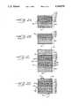
- FIGS. 1A-1Dare cross-sectional views schematically illustrating certain stages of a first embodiment of the present invention.
- FIGS. 2A-2Dare cross-sectional views schematically illustrating certain stages of a second embodiment of the present invention.
- a first method of forming a high density semiconductor structureis shown.
- a first semiconductor substrate 10 of silicon or a semiconductor material other than siliconhas grown or formed thereon a first insulating layer 25, for example a grown layer of silicon dioxide, 0.1-1.0 ⁇ m thick.
- substrate 10may be formed by forming a thin monocrystalline epitaxial layer 20, preferably 0.1 to 1.0 ⁇ m thick, on a first substrate 15.
- epitaxial layer 20is a homoepitaxial layer formed on substrate 15.
- a silicon homoepitaxial layermay be formed on a substrate in the manner disclosed in the above-referenced patents to Wanless and Abernathy, et al., or using other conventional techniques.
- the use of a homoepitaxial layermakes it difficult to etch the substrate 15 without also etching into the epitaxial layer 20.
- a preferred embodiment of the present inventionemploys a silicon heteroepitaxial layer as disclosed in application Ser. No. 07/277,617 entitled, "Method of Forming a Thin Silicon Layer on an Insulator," the disclosure of which is hereby expressly incorporated by reference, or a non-silicon heteroepitaxial layer 20 as disclosed in application Ser. No.
- Metal layer 30may take many forms, depending upon its ultimate function in the device. For example, if metal layer 30 will function as a ground plane, a single planar layer may be formed. If metal layer 30 will function as an interconnection pattern, a patterned planar layer may be formed using well known patterning techniques.
- a second substrate 40which may or may not be silicon, has a metal layer 50, for example titanium, aluminum or metal alloy, formed thereon, preferably 0.1 to 1.0 ⁇ m thick.
- metal layer 30is bonded to metal layer 50 by heating in an oxidizing ambient atmosphere to form a bonding oxide layer 35 between the metal layers 30 and 50.
- Titanium oxide (TiO 2 )forms if Ti is used and aluminum oxide (Al 2 O 3 ) forms if Al is used.
- Pressuremay be applied to the structures during bonding to aid in the bonding process and provide a higher quality bond.
- metal layer 30may be bonded to metal layer 50 by heating in an oxide ambient atmosphere to bond metal layers 30 and 50 into a single continuous metal layer.
- an oxide layermay be formed on metal layer 30 before bonding; an oxide layer may be formed on metal layer 50 before bonding; oxide layers ma be formed on both metal layers 30 and 50 before bonding; or oxide layer 35 may be formed during the bonding process as was described in connection with FIG. 1C.
- bondingmay take place in a standard annealing furnace or a rapid thermal annealing chamber, both of which are commonly available and will not be described in detail.
- the bonding time for the standard furnace at the annealing temperatureis at least 20 minutes, while in a rapid thermal annealing furnace, times between 2-4 minutes may be employed.
- An ambient atmosphere of dry oxygen and water vapormay be employed. Nitrogen, argon or other unreactive gases may also be employed with oxygen and water.
- the bonding temperatureis preferably between 600° C. to 1150° C.
- Ti--Ti structuresWhile Applicants do not wish to be bound by any theory, the chemical bond formation in Ti--Ti structures is believed to result from formation of Ti--O--Ti bonds between two Ti structures. It has been found that these bonds may be formed between two bare metal surfaces which are pressed together as a result of microscopic surface irregularities which allow oxygen to penetrate throughout the interface of the two surfaces. It will be understood by those having skill in the art that this technique of bonding two metallic surfaces via oxidation may be extended to bond other flat and smooth metallic surfaces such as aluminum, or metal alloys.
- substrate 15is removed or etched using an appropriate acid or any other commonly available etching process such as wet chemistry, plasma or reactive ion etching.
- etching processsuch as wet chemistry, plasma or reactive ion etching.
- entire substrate 10may be left intact.
- one or more viasare then formed to connect metal layer 30 with the devices in substrate 20, through insulating layer 25. If metal layer 30 is a continuous planar layer, only one via 70 may be necessary. If layer 30 is a patterned interconnection layer, a second via 60 or a large number of vias may be necessary. For purposes of illustration via 70 is shown connecting to a device within layer 20 while via 60 is connected using surface metallization 61.
- Viasmay be formed by etching through layers 20 and 25 after they are formed and filling the etched hole with metal, using well known techniques or by using well known sloped contact techniques.
- layer 25may be etched and filled after it is formed (in FIG. 1A) and layer 20 may be etched and filled after bonding (FIG. 1D) using well known self-aligned metallization techniques.
- Other well-known techniques for forming metal-filled vias in semiconductor devicesmay also be employed.
- an external connection between layers 30 and 20, rather than an internal viamay be employed. In either case, a bonded semiconductor or semiconductor on insulator structure is formed, in which a buried metal layer forms the bond between the two substrates, and acts as an interconnection pattern, resulting in a high density device.
- a second method of forming a high density semiconductor structureis shown.
- a first semiconductor substrate 100has grown or formed thereon metal layers 130, 140 and 150 with insulating layers 125, 135 and 145 therebetween.
- the composition and thicknesses of the metal and insulating layersmay be as described in connection with FIG. 1.
- substrate 100may be formed by forming a thin monocrystalline epitaxial layer 120 on a first substrate 115. Homoepitaxial or heteroepitaxial deposition may be employed.
- a plurality of vias 126selectively connect the metal layers and the substrate.
- the metal layersmay be planes or patterned metal layers.
- a second substrate 160which may or may not be a semiconductor substrate has metal layers 180 and 190 formed thereon with insulating layers 175 and 185 therebetween.
- substrate 160is a semiconductor substrate comprising epitaxial layer 170 and substrate 165.
- one via 176is shown connecting substrate 170 with buried metal layer 180.
- the topmost metal layers 150 and 190are placed in contact and bonded to one another in a heated oxidizing ambient atmosphere to form a metal-to-metal bond at 195.
- the structureis heated in an oxidizing ambient atmosphere sufficiently long enough to bond metal layers 150 and 190 into a continuous metal layer.
- metal layers 150 and 190may have an insulator formed thereon, or an insulating layer may be formed during the bonding process.
- both substrates 100 and 160need not include metal layers thereon. Rather, all the required metal layers may be fabricated on substrate 100 or 160.
- substrates 115 and/or 165are removed, as was described in connection with FIG. 1D.
- Top surface metallization 127 or internal vias 177may be selectively formed as was described in connection with FIG. 1C.
- External connectionsmay also be formed. For example, as shown in FIG. 2D, an external ground connection may be applied to buried metal layer 190.
- the structure of FIG. 2Dincludes two semiconductor device layers having a plurality of insulated buried metal layers therebetween.
- the buried metal layersmay form part or all of the device interconnection metallization so that a reduced number of surface metallization layers or no surface metallization layers may be required.
- the structure of FIG. 2Dalso forms a single package for the two devices thus connected, thus providing a high density semiconductor structure.
Landscapes
- Physics & Mathematics (AREA)
- Condensed Matter Physics & Semiconductors (AREA)
- General Physics & Mathematics (AREA)
- Engineering & Computer Science (AREA)
- Computer Hardware Design (AREA)
- Microelectronics & Electronic Packaging (AREA)
- Power Engineering (AREA)
- Internal Circuitry In Semiconductor Integrated Circuit Devices (AREA)
Abstract
Description
This application is a divisional of application Ser. No. 07/277,607, filed on Nov. 29, 1988, now U.S. Pat. No. 5,025,304.
This invention relates to the fabrication of semiconductor wafers for subsequent formation into semiconductor and integrated circuit devices, and more specifically to a semiconductor fabrication method in which high density devices and high density device interconnection patterns may be formed.
High density semiconductor fabrication techniques are required for the manufacture of Very Large Scale Integration (VLSI) and Ultra Large Scale Integration (ULSI) chips having up to several million devices thereon. High density chips may be fabricated by shrinking the size of the individual devices on the chips so that more devices per unit area may be formed. When device sizes shrink, however, it becomes more difficult to provide interconnection between devices. If small size devices cannot be connected to one another as required, the benefits of small device size are lost.
The art has provided many techniques for forming dense metal interconnection patterns for device interconnection. High density VLSI and ULSI devices typically require multiple levels of surface metallization in order to accommodate their complex wiring patterns. Unfortunately, multiple level metallization creates planarity problems in the metallization layers, thereby limiting interconnection density. Complex process steps are also needed to provide multiple levels of metallization.
Another concern in shrinking device size is the difficulty of providing adequate isolation between devices. Semiconductor On Insulator (SOI) technology may be employed to enhance isolation between devices. One method for fabricating an SOI structure oxidizes first and second silicon substrates to form a layer of silicon dioxide (SiO2) on each. The silicon dioxide surfaces ar bonded together face-to-face to form a unified structure. Most of the silicon may be etched from one of the wafers until only several micrometers of silicon remain. Devices are then formed in this thin film of silicon. Another version of this type of silicon oxide bonding technique is disclosed in an article by Laskey entitled "Wafer Bonding for Silicon-On-Insulator Technologies," Applied Physics Letters, Vol. 48, No. 1, Jan. 6, 1986. Other examples of silicon oxide bonding techniques are disclosed in U.S. Pat. No. 3,997,381 to Wanlass, and in U.S. Pat. No. 4,601,779 to Abernathy et al.
In accordance with the foregoing, it is an object of the present invention to provide a method of fabricating a high density semiconductor structure.
It is another object of the present invention to provide a method of making a high density semiconductor structure in which high density interconnection patterns may be formed.
It is yet another object of the present invention to provide a method of making a high density semiconductor structure which maintains a high degree of device isolation.
These and other objects are met according to the present invention by providing a metal to metal bonding technique for joining two substrates to form a semiconductor structure, while at the same time providing a buried metal layer within the device for device interconnection. The very same metal layer which forms the bond for a semiconductor device also forms at least part of the device interconnection pattern. Surface metallization patterns are thus simplified resulting in high density devices with high density interconnection patterns.
According to the present invention, one or more metal layers are formed on a first semiconductor substrate, with the metal layer or layers being insulated from one another and from the substrate except at desired contacting regions. One or more metal layers are formed on a second substrate which may or may not be a semiconductor substrate. The topmost metal layer on the two substrates are placed against one another, and are heated in an oxidizing ambient atmosphere to form a bond therebetween. Either or both of the topmost metal layers may include an oxide layer on the surface thereof. Devices may then be formed in the first semiconductor substrate and in the second substrate if it is also a semiconductor substrate.
The structure formed according to the present invention includes a semiconductor substrate with one or more buried metal layers, or two semiconductor substrates with one or more buried metal layers therebetween. The buried metal layers of the present invention not only form part of the metal to metal bond, but also form part of the device interconnection metallization, so that all of the device interconnection need not be accomplished with surface metallization. Fewer surface metallization layers may be employed, resulting in denser interconnection patterns. In this regard, some of the buried metal layers may be planar layers for use as a ground or power plane, or as a radiation hardening shield. Alternatively, or in addition to planar layers, patterned layers may be formed for device interconnection. The buried metal layers together with the buried insulator regions may also form one or more buried capacitors for use with the active devices. It will be understood by those having skill in the art that the buried metal layers may be connected to one another and to the devices in the first substrate (and the second substrate if semiconductor), using metal vias which run through the insulating layers between buried metal layers, or using sloped contacts between buried metal layers. Well known techniques may be employed to form these vias or sloped contacts. External connections may also be employed instead of, or in addition to, the internal vias or sloped contacts.
The buried metal layers of the present invention may be metal or metal alloy. They need not all be of the same metal. The metal-to-metal bonding may bond the two metal layers to form a single metal layer. Alternatively, an oxide bonding layer sufficiently thick to form an insulator between the topmost metal layers may be formed.
The present invention may also be employed to form a semiconductor on insulator structure having one or more buried layers. In order to form a semiconductor on insulator structure, the first semiconductor substrate is formed by epitaxial deposition on a first substrate. The metal layer or layers as described above are then formed on the epitaxial layer. After bonding, the first substrate is removed, to expose the epitaxial layer. Similar steps may be employed with the second substrate, if semiconductor. In a preferred embodiment of the invention, the epitaxial layer on the substrate is a heteroepitaxial layer, so that the substrate may be easily etched after bonding to expose the heteroepitaxial layer. As is well known to those having skill in the art, the epitaxial growth process is a means for depositing a thin layer of a single crystal material on a single crystal substrate. If the film is the same material as the substrate (for example silicon deposition on a silicon substrate), the process is called homoepitaxy. If, on the other hand, the deposit is made on a substrate that is chemically different (for example silicon deposition on a non-silicon substrate), the process is called heteroepitaxy. By providing chemically different materials for the substrate and epitaxial layer, removal of the substrate is facilitated.
FIGS. 1A-1D are cross-sectional views schematically illustrating certain stages of a first embodiment of the present invention.
FIGS. 2A-2D are cross-sectional views schematically illustrating certain stages of a second embodiment of the present invention.
The present invention now will be described more fully hereinafter with reference to the accompanying drawings, in which a preferred embodiment of the invention is shown. This invention may, however, be embodied in many different forms and should not be construed as limited to the embodiment set forth herein; rather, applicants provide this embodiment so that this disclosure will be thorough and complete, and will fully convey the scope of the invention to those skilled in the art.
Like characters refer to like elements throughout. For greater clarity, the thickness of layers has been exaggerated.
Referring to FIGS. 1A-1D, a first method of forming a high density semiconductor structure according to the present invention is shown. In FIG. 1A, afirst semiconductor substrate 10 of silicon or a semiconductor material other than silicon has grown or formed thereon a first insulatinglayer 25, for example a grown layer of silicon dioxide, 0.1-1.0 μm thick. In order to form a semiconductor on insulator structure, rather than a conventional semiconductor structure,substrate 10 may be formed by forming a thinmonocrystalline epitaxial layer 20, preferably 0.1 to 1.0 μm thick, on afirst substrate 15. In one embodiment of the invention,epitaxial layer 20 is a homoepitaxial layer formed onsubstrate 15. For example, a silicon homoepitaxial layer may be formed on a substrate in the manner disclosed in the above-referenced patents to Wanless and Abernathy, et al., or using other conventional techniques. The use of a homoepitaxial layer makes it difficult to etch thesubstrate 15 without also etching into theepitaxial layer 20. Accordingly, a preferred embodiment of the present invention employs a silicon heteroepitaxial layer as disclosed in application Ser. No. 07/277,617 entitled, "Method of Forming a Thin Silicon Layer on an Insulator," the disclosure of which is hereby expressly incorporated by reference, or a non-siliconheteroepitaxial layer 20 as disclosed in application Ser. No. 07/277,168 entitled, "Method of Forming a Non-Silicon Semiconductor on Insulator Structure," now U.S. Pat. No. 4,891,329, dated Jan. 2, 1990, the disclosure of which is hereby expressly incorporated by reference.
Referring now to FIG. 1B, ametal layer 30, preferably 0.1 to 1.0 μm thick, such as titanium, aluminum or a metal alloy, is then grown or formed on the insulatinglayer 25. It will be understood by those having skill in the art that insulatinglayer 25 protectsepitaxial layer 20 from contactingmetal layer 30 except where desired.Metal layer 30 may take many forms, depending upon its ultimate function in the device. For example, ifmetal layer 30 will function as a ground plane, a single planar layer may be formed. Ifmetal layer 30 will function as an interconnection pattern, a patterned planar layer may be formed using well known patterning techniques.
Referring now to FIG. 1C, asecond substrate 40, which may or may not be silicon, has ametal layer 50, for example titanium, aluminum or metal alloy, formed thereon, preferably 0.1 to 1.0 μm thick. Then,metal layer 30 is bonded tometal layer 50 by heating in an oxidizing ambient atmosphere to form abonding oxide layer 35 between the metal layers 30 and 50. Titanium oxide (TiO2) forms if Ti is used and aluminum oxide (Al2 O3) forms if Al is used. Pressure may be applied to the structures during bonding to aid in the bonding process and provide a higher quality bond.
It will be understood by those having skill in the art that adiscrete oxide layer 35 need not be formed during the bonding process. In other words,metal layer 30 may be bonded tometal layer 50 by heating in an oxide ambient atmosphere to bond metal layers 30 and 50 into a single continuous metal layer. If an oxide layer is desired betweenmetal layers metal layer 30 before bonding; an oxide layer may be formed onmetal layer 50 before bonding; oxide layers ma be formed on bothmetal layers oxide layer 35 may be formed during the bonding process as was described in connection with FIG. 1C.
According to the invention, bonding may take place in a standard annealing furnace or a rapid thermal annealing chamber, both of which are commonly available and will not be described in detail. Preferably, the bonding time for the standard furnace at the annealing temperature is at least 20 minutes, while in a rapid thermal annealing furnace, times between 2-4 minutes may be employed. An ambient atmosphere of dry oxygen and water vapor may be employed. Nitrogen, argon or other unreactive gases may also be employed with oxygen and water. The bonding temperature is preferably between 600° C. to 1150° C. For example, titanium (Ti) to Ti bonded very well in oxidizing atmospheres at temperatures greater than or near 700° C. in a conventional furnace for twenty minutes.
While Applicants do not wish to be bound by any theory, the chemical bond formation in Ti--Ti structures is believed to result from formation of Ti--O--Ti bonds between two Ti structures. It has been found that these bonds may be formed between two bare metal surfaces which are pressed together as a result of microscopic surface irregularities which allow oxygen to penetrate throughout the interface of the two surfaces. It will be understood by those having skill in the art that this technique of bonding two metallic surfaces via oxidation may be extended to bond other flat and smooth metallic surfaces such as aluminum, or metal alloys.
This method of bonding metal surfaces is disclosed in an application filed concurrently herewith, application Ser. No. 07/277,620, entitled "Metal-to-Metal Bonding Method and Resulting Structure," now U.S. Pat. No. 4,009,360, the disclosure of which is expressly incorporated herein by reference.
Referring again to FIG. 1C, if a semiconductor on insulator structure is to be formed,substrate 15 is removed or etched using an appropriate acid or any other commonly available etching process such as wet chemistry, plasma or reactive ion etching. For a conventional semiconductor structure,entire substrate 10 may be left intact. Referring now to FIG. 1D, one or more vias are then formed to connectmetal layer 30 with the devices insubstrate 20, through insulatinglayer 25. Ifmetal layer 30 is a continuous planar layer, only one via 70 may be necessary. Iflayer 30 is a patterned interconnection layer, a second via 60 or a large number of vias may be necessary. For purposes of illustration via 70 is shown connecting to a device withinlayer 20 while via 60 is connected usingsurface metallization 61. Vias may be formed by etching throughlayers layer 25 may be etched and filled after it is formed (in FIG. 1A) andlayer 20 may be etched and filled after bonding (FIG. 1D) using well known self-aligned metallization techniques. Other well-known techniques for forming metal-filled vias in semiconductor devices may also be employed. Alternatively, an external connection betweenlayers
Referring to FIGS. 2A-2D, a second method of forming a high density semiconductor structure according to the present invention is shown. In FIG. 2A, afirst semiconductor substrate 100 has grown or formed thereonmetal layers layers substrate 100 may be formed by forming a thinmonocrystalline epitaxial layer 120 on afirst substrate 115. Homoepitaxial or heteroepitaxial deposition may be employed. A plurality ofvias 126 selectively connect the metal layers and the substrate. As was described in connection with FIG. 1, the metal layers may be planes or patterned metal layers.
Referring now to FIG. 2B, asecond substrate 160 which may or may not be a semiconductor substrate hasmetal layers layers substrate 160 is a semiconductor substrate comprisingepitaxial layer 170 andsubstrate 165. For purposes of illustration, one via 176 is shown connectingsubstrate 170 with buriedmetal layer 180. Referring now to FIG. 2C, thetopmost metal layers
Referring now to FIG. 2C, the structure is heated in an oxidizing ambient atmosphere sufficiently long enough to bond metal layers 150 and 190 into a continuous metal layer. As was described in connection with respect to FIG. 1C, either or bothmetal layers substrates substrate
Referring now to FIG. 2D, if one or two semiconductor on insulator structures are to be formed,substrates 115 and/or 165 are removed, as was described in connection with FIG. 1D.Top surface metallization 127 orinternal vias 177 may be selectively formed as was described in connection with FIG. 1C. External connections may also be formed. For example, as shown in FIG. 2D, an external ground connection may be applied to buriedmetal layer 190.
The structure of FIG. 2D includes two semiconductor device layers having a plurality of insulated buried metal layers therebetween. The buried metal layers may form part or all of the device interconnection metallization so that a reduced number of surface metallization layers or no surface metallization layers may be required. The structure of FIG. 2D also forms a single package for the two devices thus connected, thus providing a high density semiconductor structure.
In the drawings and specification, there have been disclosed typical preferred embodiments of the invention and, although specific terms are employed, they are used in a generic and descriptive sense only and not for purposes of limitation, the scope of the invention being set forth in the following claims.
Claims (43)
1. A method of forming a semiconductor device comprising the steps of:
(a) providing a first semiconductor substrate;
(b) providing a second substrate;
(c) forming at least one metal layer on at least one of said first semiconductor substrate and said second substrate;
(d) placing said first semiconductor substrate and said second substrate against one another with said at least one metal layer therebetween; and
(e) heating in an oxidizing ambient atmosphere to bond said first semiconductor substrate to said second substrate and form a buried metal layer semiconductor device.
2. The method of claim 1 wherein the step of forming at least one metal layer on at least one of said first semiconductor substrate and said second substrate comprises the steps of:
forming at least a first metal layer on said first semiconductor substrate; and
forming at least a second metal layer on said second substrate.
3. The method of claim 1 wherein the step of forming at least one metal layer on at least one of said first semiconductor substrate and said second substrate comprises the steps of:
forming a first insulating layer on said first semiconductor substrate; and
forming a first metal layer on said first insulating layer.
4. The method of claim 1 wherein the step of forming at least one metal layer on at least one of said first semiconductor substrate and said second substrate comprises the step of forming a plurality of metal layers on said first semiconductor substrate, said plurality of metal layers being insulated from one another and from said first semiconductor substrate.
5. The method of claim 1 wherein the step of forming at least one metal layer on at least one of said first semiconductor substrate and said second substrate comprises the step of forming a plurality of metal layers on said second substrate, said plurality of metal layers being separated from one another by insulating layers.
6. The method of claim 1 wherein the step of providing a second substrate comprises the step of providing a second semiconductor substrate.
7. The method of claim 1 wherein said second substrate is a second semiconductor substrate, and wherein the step of forming at least one metal layer on at least one of said first semiconductor substrate and said second substrate comprises the step of forming a plurality of metal layers on said second semiconductor substrate, said plurality of metal layers being insulated from one another and from said second semiconductor substrate.
8. The method of claim 3 wherein the step of providing a first semiconductor substrate comprises the step of providing an epitaxial layer on a first substrate; wherein the step of forming a first insulating layer on said first semiconductor substrate comprises the step of forming a first insulating layer on said epitaxial layer; and wherein said heating step is followed by the step of removing said first substrate.
9. The method of claim 4 wherein the step of providing a first semiconductor substrate comprises the step of providing an epitaxial layer on a first substrate; wherein the step of forming a plurality of metal layers on said first semiconductor substrate comprises the step of forming a plurality of metal layers on said epitaxial layer; and wherein said heating step is followed by the step of removing said first substrate.
10. The method of claim 7 wherein said second semiconductor substrate comprises an epitaxial layer on a second substrate, wherein the step of forming a plurality of metal layers on said second semiconductor substrate comprises the step of forming an insulating layer on said epitaxial layer; and wherein said heating step is followed by the step of removing said second substrate.
11. The method of claim 7 wherein said second semiconductor substrate comprises an epitaxial layer on a second substrate; wherein the step of forming a plurality of metal layers on said second semiconductor substrate comprises the step of forming a plurality of metal layers on said epitaxial layer; and wherein said heating step is followed by the step of removing said second substrate.
12. The method of claim 1 wherein the placing step is preceded by the step of forming an insulating layer on said at least one metal layer.
13. The method of claim 12 wherein said insulating layer is a metal oxide layer.
14. The method of claim 2 wherein the placing step is preceded by the step of forming an insulating layer on at least one of said first and said second metal layers.
15. The method of claim 14 wherein said insulating layer is a metal oxide layer.
16. The method of claim 1 wherein said heating step comprises the step of heating in an oxidizing ambient atmosphere to form an oxide insulating layer and a bond between said first and second substrates.
17. The method of claim 1 further comprising the step of:
forming an electrical connection between sad at least one metal layer and said first semiconductor substrate.
18. The method of claim 3 further comprising the step of:
forming an electrical connection between said first metal layer and said first semiconductor substrate.
19. The method of claim 18 wherein the step of forming an electrical connection comprises the step of forming an electrical connection through said first insulating layer.
20. The method of claim 4 further comprising the step of:
forming electrical connections between at least one of said plurality of metal layers and said first semiconductor substrate.
21. The method of claim 5 further comprising the step of:
forming electrical connections between at least one of said plurality of metal layers and said first semiconductor substrate.
22. The method of claim 1 wherein the step of forming at least on metal layer comprises the step of forming at least one patterned metal layer.
23. The method of claim 4 wherein the step of forming a plurality of metal layers on said first semiconductor substrate comprises the step of forming at least one patterned metal layer among said plurality of metal layers.
24. The method of claim 5 wherein the step of forming a plurality of metal layers on said second substrate comprises the step of forming at least one patterned metal layer among said plurality of metal layers.
25. The method of claim 5 wherein the step of forming a plurality of metal layers on said second semiconductor substrate comprises the step of forming at least one patterned metal layer among said plurality of metal layers.
26. The method of claim 1 wherein said at least one metal layer is selected from the group consisting of Ti and Al.
27. The method of claim 1 wherein said at least one metal layer is at least one metal alloy layer.
28. The method of claim 1 wherein said heating step comprises the step of heating in an oxidizing ambient atmosphere while simultaneously applying pressure between said first and second substrates to form a bond therebetween.
29. The method of claim 1 wherein said heating step comprises the step of heating said first and second substrates at a temperature between 700° C. and 1200° C.
30. The method of claim 1 wherein said oxidizing ambient atmosphere consists essentially of water vapor and oxygen.
31. A method of forming a semiconductor device comprising the steps of:
providing a first semiconductor substrate;
forming a first plurality of metal layers on said first semiconductor substrate, said first plurality of metal layers being insulated from one another and from said first semiconductor substrate,
providing a second substrate;
forming a second plurality of metal layers on said second substrate, said second plurality of metal layers being insulated from one another;
placing said first and second plurality of metal layers against one another; and
heating said first and second plurality of metal layers in an oxidizing ambient atmosphere to form a bond therebetween.
32. The method of claim 31 wherein said second substrate is a second semiconductor substrate.
33. The method of claim 31 wherein said heating step comprises the step of heating said first and second plurality of metal layers to form an oxide insulating layer and a bond therebetween.
34. The method of claim 31 further comprising the step of forming electrical connections between selective ones of said first and second plurality of metal layers and said semiconductor substrate.
35. The method of claim 31 wherein the step of providing a first semiconductor substrate comprises the step of providing an epitaxial layer on a first substrate; wherein the step of forming a first plurality of metal layers on said first semiconductor substrate comprises the step of forming said first plurality of metal layers on said epitaxial layer; and wherein said heating step is followed by the step of removing said first substrate.
36. The method of claim 32 wherein the step of providing a second semiconductor substrate comprises the step of providing an epitaxial layer on a second substrate; wherein the step of forming a second plurality of metal layers on said second semiconductor substrate comprises the step of forming said second plurality of metal layers on said epitaxial layer; and wherein said heating step is followed by the step of removing said second substrate.
37. The method of claim 31 wherein the step of forming a first plurality of metal layers on said first semiconductor substrate comprises the step of forming at least one patterned metal layer among said first plurality of metal layers.
38. The method of claim 31 wherein the step of forming a second plurality of metal layers on said second semiconductor substrate comprises the step of forming at least one patterned metal layer among said second plurality of metal layers.
39. The method of claim 31 wherein said first and second plurality of metal layers are selected from the group consisting of Ti and Al.
40. The method of claim 31 wherein said first and second plurality of metal layers are metal alloy layers.
41. The method of claim 31 wherein said heating step comprises the step of heating said first and second plurality of metal layers in an oxidizing ambient atmosphere while simultaneously applying pressure between said first and second plurality of metal layers to form a bond therebetween.
42. The method of claim 31 wherein said heating step comprises the step of heating said first and second plurality of metal layers at a temperature between 700° C. and 1200° C.
43. The method of claim 31 wherein said oxidizing ambient atmosphere consists essentially of water vapor and oxygen.
Priority Applications (1)
| Application Number | Priority Date | Filing Date | Title |
|---|---|---|---|
| US07/631,671US5168078A (en) | 1988-11-29 | 1990-12-21 | Method of making high density semiconductor structure |
Applications Claiming Priority (2)
| Application Number | Priority Date | Filing Date | Title |
|---|---|---|---|
| US07/277,607US5025304A (en) | 1988-11-29 | 1988-11-29 | High density semiconductor structure and method of making the same |
| US07/631,671US5168078A (en) | 1988-11-29 | 1990-12-21 | Method of making high density semiconductor structure |
Related Parent Applications (1)
| Application Number | Title | Priority Date | Filing Date |
|---|---|---|---|
| US07/277,607DivisionUS5025304A (en) | 1988-11-29 | 1988-11-29 | High density semiconductor structure and method of making the same |
Publications (1)
| Publication Number | Publication Date |
|---|---|
| US5168078Atrue US5168078A (en) | 1992-12-01 |
Family
ID=26958591
Family Applications (1)
| Application Number | Title | Priority Date | Filing Date |
|---|---|---|---|
| US07/631,671Expired - Fee RelatedUS5168078A (en) | 1988-11-29 | 1990-12-21 | Method of making high density semiconductor structure |
Country Status (1)
| Country | Link |
|---|---|
| US (1) | US5168078A (en) |
Cited By (31)
| Publication number | Priority date | Publication date | Assignee | Title |
|---|---|---|---|---|
| US5256581A (en)* | 1991-08-28 | 1993-10-26 | Motorola, Inc. | Silicon film with improved thickness control |
| US5260233A (en)* | 1992-11-06 | 1993-11-09 | International Business Machines Corporation | Semiconductor device and wafer structure having a planar buried interconnect by wafer bonding |
| US5324678A (en)* | 1989-09-22 | 1994-06-28 | Mitsubishi Denki Kabushiki Kaisha | Method of forming a multi-layer type semiconductor device with semiconductor element layers stacked in opposite directions |
| US5387551A (en)* | 1992-03-04 | 1995-02-07 | Kabushiki Kaisha Toshiba | Method of manufacturing flat inductance element |
| WO1995010410A1 (en)* | 1993-10-14 | 1995-04-20 | Intevac, Inc. | Pseudomorphic substrates |
| US5413952A (en)* | 1994-02-02 | 1995-05-09 | Motorola, Inc. | Direct wafer bonded structure method of making |
| US5413955A (en)* | 1993-12-21 | 1995-05-09 | Delco Electronics Corporation | Method of bonding silicon wafers at temperatures below 500 degrees centigrade for sensor applications |
| US5449659A (en)* | 1991-07-05 | 1995-09-12 | Conductus, Inc. | Method of bonding multilayer structures of crystalline materials |
| US5536361A (en)* | 1992-01-31 | 1996-07-16 | Canon Kabushiki Kaisha | Process for preparing semiconductor substrate by bonding to a metallic surface |
| US5580802A (en)* | 1994-09-22 | 1996-12-03 | Aerospace Corp | Silicon-on-insulator gate-all-around mosfet fabrication methods |
| US5589419A (en)* | 1994-07-26 | 1996-12-31 | Sony Corporation | Process for fabricating semiconductor device having a multilevel interconnection |
| US5674758A (en)* | 1995-06-06 | 1997-10-07 | Regents Of The University Of California | Silicon on insulator achieved using electrochemical etching |
| US5702957A (en)* | 1996-09-20 | 1997-12-30 | Lsi Logic Corporation | Method of making buried metallization structure |
| US5712747A (en)* | 1996-01-24 | 1998-01-27 | International Business Machines Corporation | Thin film slider with on-board multi-layer integrated circuit |
| US5849627A (en)* | 1990-02-07 | 1998-12-15 | Harris Corporation | Bonded wafer processing with oxidative bonding |
| US6004865A (en)* | 1993-09-06 | 1999-12-21 | Hitachi, Ltd. | Method of fabricating multi-layered structure having single crystalline semiconductor film formed on insulator |
| US6045625A (en)* | 1996-12-06 | 2000-04-04 | Texas Instruments Incorporated | Buried oxide with a thermal expansion matching layer for SOI |
| US6174803B1 (en) | 1998-09-16 | 2001-01-16 | Vsli Technology | Integrated circuit device interconnection techniques |
| US6309945B1 (en)* | 1992-01-31 | 2001-10-30 | Canon Kabushiki Kaisha | Process for producing semiconductor substrate of SOI structure |
| US6368964B1 (en)* | 2000-12-08 | 2002-04-09 | United Microelectronics Corp. | Method for reducing resistance in a conductor |
| US6743662B2 (en)* | 2002-07-01 | 2004-06-01 | Honeywell International, Inc. | Silicon-on-insulator wafer for RF integrated circuit |
| US20040229443A1 (en)* | 1998-12-31 | 2004-11-18 | Bower Robert W. | Structures, materials and methods for fabrication of nanostructures by transposed split of ion cut materials |
| US6909146B1 (en) | 1992-02-12 | 2005-06-21 | Intersil Corporation | Bonded wafer with metal silicidation |
| US20050149286A1 (en)* | 2003-12-03 | 2005-07-07 | Burak Acar | Heat diffusion based detection of structures of interest in medical images |
| US20050162043A1 (en)* | 2003-12-01 | 2005-07-28 | Takamitsu Higuchi | Piezoelectric device, liquid jet head, and methods for manufacturing the same, and thin film forming apparatus |
| US7297613B1 (en)* | 2005-06-09 | 2007-11-20 | The United States Of America As Represented By The National Security Agency | Method of fabricating and integrating high quality decoupling capacitors |
| US20080166582A1 (en)* | 2007-01-08 | 2008-07-10 | Chuanbing Xiong | Method for fabricating metal substrates with high-quality surfaces |
| US20090246946A1 (en)* | 2008-03-31 | 2009-10-01 | Emmanuel Augendre | Method of fabricating a microelectronic structure of a semiconductor on insulator type with different patterns |
| US7863654B2 (en) | 1998-12-21 | 2011-01-04 | Megica Corporation | Top layers of metal for high performance IC's |
| US20140274725A1 (en)* | 2013-03-15 | 2014-09-18 | International Business Machines Corporation | Chip mode isolation and cross-talk reduction through buried metal layers and through-vias |
| US9219298B2 (en) | 2013-03-15 | 2015-12-22 | International Business Machines Corporation | Removal of spurious microwave modes via flip-chip crossover |
Citations (27)
| Publication number | Priority date | Publication date | Assignee | Title |
|---|---|---|---|---|
| US3725743A (en)* | 1971-05-19 | 1973-04-03 | Hitachi Ltd | Multilayer wiring structure |
| US3766445A (en)* | 1970-08-10 | 1973-10-16 | Cogar Corp | A semiconductor substrate with a planar metal pattern and anodized insulating layers |
| US3997381A (en)* | 1975-01-10 | 1976-12-14 | Intel Corporation | Method of manufacture of an epitaxial semiconductor layer on an insulating substrate |
| US4200474A (en)* | 1978-11-20 | 1980-04-29 | Texas Instruments Incorporated | Method of depositing titanium dioxide (rutile) as a gate dielectric for MIS device fabrication |
| US4245768A (en)* | 1978-07-28 | 1981-01-20 | The Unites States Of America As Represented By The Administrator Of The National Aeronautics And Space Administration | Method of cold welding using ion beam technology |
| US4247034A (en)* | 1977-09-23 | 1981-01-27 | Siemens Aktiengesellschaft | Method of indirectly connecting two parts |
| US4288470A (en)* | 1978-12-11 | 1981-09-08 | Texas Instruments Incorporated | Method of making non-volatile semiconductor memory elements having multiple dielectric layers of silicon nitride, silicon dioxide, and rutile titanium dioxide |
| JPS5886751A (en)* | 1981-11-18 | 1983-05-24 | Mitsubishi Electric Corp | Stacked semiconductor device |
| JPS58103149A (en)* | 1981-12-15 | 1983-06-20 | Matsushita Electric Works Ltd | Semiconductor device |
| US4411962A (en)* | 1981-12-08 | 1983-10-25 | Vought Corporation | Induced or constrained superplastic laminates for forming |
| US4481283A (en)* | 1982-04-30 | 1984-11-06 | U.S. Philips Corporation | Method of manufacturing an integrated capacitor and device obtained by this method |
| JPS603148A (en)* | 1983-06-21 | 1985-01-09 | Nec Corp | Substrate for single crystal silicon semiconductor device and manufacture thereof |
| US4495219A (en)* | 1981-10-09 | 1985-01-22 | Fujitsu Limited | Process for producing dielectric layers for semiconductor devices |
| JPS6021553A (en)* | 1983-07-15 | 1985-02-02 | Hitachi Ltd | three dimensional integrated circuit |
| JPS60117690A (en)* | 1983-11-30 | 1985-06-25 | Fujitsu Ltd | Semiconductor device |
| US4596604A (en)* | 1983-10-22 | 1986-06-24 | Agency Of Industrial Science And Technology | Method of manufacturing a multilayer semiconductor device |
| JPS61174661A (en)* | 1985-01-29 | 1986-08-06 | Nippon Telegr & Teleph Corp <Ntt> | Semiconductor integrated circuit device and manufacture thereof |
| JPS61182216A (en)* | 1985-02-08 | 1986-08-14 | Toshiba Corp | Bonding method of semiconductor device |
| US4636833A (en)* | 1983-03-18 | 1987-01-13 | Hitachi, Ltd. | Semiconductor device |
| JPS62145850A (en)* | 1985-12-20 | 1987-06-29 | Fujitsu Ltd | semiconductor equipment |
| EP0238066A2 (en)* | 1986-03-18 | 1987-09-23 | Fujitsu Limited | A method for effecting adhesion of silicon or silicon dioxide plates |
| US4704512A (en)* | 1985-02-25 | 1987-11-03 | Peter Lisec | Apparatus for butt welding |
| EP0256397A1 (en)* | 1986-07-31 | 1988-02-24 | Hitachi, Ltd. | Semiconductor device having a burried layer |
| US4732312A (en)* | 1986-11-10 | 1988-03-22 | Grumman Aerospace Corporation | Method for diffusion bonding of alloys having low solubility oxides |
| JPS63260051A (en)* | 1987-04-16 | 1988-10-27 | Nec Corp | Semiconductor device |
| US4891329A (en)* | 1988-11-29 | 1990-01-02 | University Of North Carolina | Method of forming a nonsilicon semiconductor on insulator structure |
| EP0371861A2 (en)* | 1988-11-29 | 1990-06-06 | Mcnc | High density semiconductor structure and method of making the same |
- 1990
- 1990-12-21USUS07/631,671patent/US5168078A/ennot_activeExpired - Fee Related
Patent Citations (27)
| Publication number | Priority date | Publication date | Assignee | Title |
|---|---|---|---|---|
| US3766445A (en)* | 1970-08-10 | 1973-10-16 | Cogar Corp | A semiconductor substrate with a planar metal pattern and anodized insulating layers |
| US3725743A (en)* | 1971-05-19 | 1973-04-03 | Hitachi Ltd | Multilayer wiring structure |
| US3997381A (en)* | 1975-01-10 | 1976-12-14 | Intel Corporation | Method of manufacture of an epitaxial semiconductor layer on an insulating substrate |
| US4247034A (en)* | 1977-09-23 | 1981-01-27 | Siemens Aktiengesellschaft | Method of indirectly connecting two parts |
| US4245768A (en)* | 1978-07-28 | 1981-01-20 | The Unites States Of America As Represented By The Administrator Of The National Aeronautics And Space Administration | Method of cold welding using ion beam technology |
| US4200474A (en)* | 1978-11-20 | 1980-04-29 | Texas Instruments Incorporated | Method of depositing titanium dioxide (rutile) as a gate dielectric for MIS device fabrication |
| US4288470A (en)* | 1978-12-11 | 1981-09-08 | Texas Instruments Incorporated | Method of making non-volatile semiconductor memory elements having multiple dielectric layers of silicon nitride, silicon dioxide, and rutile titanium dioxide |
| US4495219A (en)* | 1981-10-09 | 1985-01-22 | Fujitsu Limited | Process for producing dielectric layers for semiconductor devices |
| JPS5886751A (en)* | 1981-11-18 | 1983-05-24 | Mitsubishi Electric Corp | Stacked semiconductor device |
| US4411962A (en)* | 1981-12-08 | 1983-10-25 | Vought Corporation | Induced or constrained superplastic laminates for forming |
| JPS58103149A (en)* | 1981-12-15 | 1983-06-20 | Matsushita Electric Works Ltd | Semiconductor device |
| US4481283A (en)* | 1982-04-30 | 1984-11-06 | U.S. Philips Corporation | Method of manufacturing an integrated capacitor and device obtained by this method |
| US4636833A (en)* | 1983-03-18 | 1987-01-13 | Hitachi, Ltd. | Semiconductor device |
| JPS603148A (en)* | 1983-06-21 | 1985-01-09 | Nec Corp | Substrate for single crystal silicon semiconductor device and manufacture thereof |
| JPS6021553A (en)* | 1983-07-15 | 1985-02-02 | Hitachi Ltd | three dimensional integrated circuit |
| US4596604A (en)* | 1983-10-22 | 1986-06-24 | Agency Of Industrial Science And Technology | Method of manufacturing a multilayer semiconductor device |
| JPS60117690A (en)* | 1983-11-30 | 1985-06-25 | Fujitsu Ltd | Semiconductor device |
| JPS61174661A (en)* | 1985-01-29 | 1986-08-06 | Nippon Telegr & Teleph Corp <Ntt> | Semiconductor integrated circuit device and manufacture thereof |
| JPS61182216A (en)* | 1985-02-08 | 1986-08-14 | Toshiba Corp | Bonding method of semiconductor device |
| US4704512A (en)* | 1985-02-25 | 1987-11-03 | Peter Lisec | Apparatus for butt welding |
| JPS62145850A (en)* | 1985-12-20 | 1987-06-29 | Fujitsu Ltd | semiconductor equipment |
| EP0238066A2 (en)* | 1986-03-18 | 1987-09-23 | Fujitsu Limited | A method for effecting adhesion of silicon or silicon dioxide plates |
| EP0256397A1 (en)* | 1986-07-31 | 1988-02-24 | Hitachi, Ltd. | Semiconductor device having a burried layer |
| US4732312A (en)* | 1986-11-10 | 1988-03-22 | Grumman Aerospace Corporation | Method for diffusion bonding of alloys having low solubility oxides |
| JPS63260051A (en)* | 1987-04-16 | 1988-10-27 | Nec Corp | Semiconductor device |
| US4891329A (en)* | 1988-11-29 | 1990-01-02 | University Of North Carolina | Method of forming a nonsilicon semiconductor on insulator structure |
| EP0371861A2 (en)* | 1988-11-29 | 1990-06-06 | Mcnc | High density semiconductor structure and method of making the same |
Non-Patent Citations (14)
| Title |
|---|
| Field Assisted Bonding Below 200 C. Using Metal and Glass Thin Film Interlayers, W. Y. Lee et al., Applied Physics Letters, 50(9), Mar. 2, 1987, pp. 522 524.* |
| Field-Assisted Bonding Below 200° C. Using Metal and Glass Thin-Film Interlayers, W. Y. Lee et al., Applied Physics Letters, 50(9), Mar. 2, 1987, pp. 522-524. |
| Joining and Recrystallization of Si Using the Thermomigration Process, T. Mizrah, 1980 American Institute of Physics, J. Appl. Phys. 51(2), Feb. 1980, pp. 1207 1210.* |
| Joining and Recrystallization of Si Using the Thermomigration Process, T. Mizrah, 1980 American Institute of Physics, J. Appl. Phys. 51(2), Feb. 1980, pp. 1207-1210. |
| Nayak et al., Metal to Metal Bonding Using an Oxidizing Ambient Atmosphere, Journal of the Electrochemical Society, vol. 135, No. 4, Apr. 1988, pp. 1023 1025.* |
| Nayak et al., Metal-to-Metal Bonding Using an Oxidizing Ambient Atmosphere, Journal of the Electrochemical Society, vol. 135, No. 4, Apr. 1988, pp. 1023-1025. |
| Promissing New Fabrication Process Developed For Stacked LSI s, M. Yasumoto et al., IEDM Technical Digest, 1984, pp. 816 819.* |
| Promissing New Fabrication Process Developed For Stacked LSI's, M. Yasumoto et al., IEDM Technical Digest, 1984, pp. 816-819. |
| Sorab Ghandi, VLSI Fabrication Principles, John Wiley & Sons, New York, N.Y. (1983), pp. 214 216.* |
| Sorab Ghandi, VLSI Fabrication Principles, John Wiley & Sons, New York, N.Y. (1983), pp. 214-216. |
| Thomas R. Anthony, "Dielectric Isolation of Silicon by Anodic Bonding", Aug. 1, 1985, Journal of Applied Physics, pp. 1240-1247. |
| Thomas R. Anthony, Dielectric Isolation of Silicon by Anodic Bonding , Aug. 1, 1985, Journal of Applied Physics, pp. 1240 1247.* |
| W. P. Mazara, G. Goetz, A. Caviglia and J. B. McKittrick, "Bonding of Silicon Wafers for Silicon-On Insulator", Journal of Applied Physics (Nov. 15, 1988), vol. 64, No. 10, pp. 4943-4950. |
| W. P. Mazara, G. Goetz, A. Caviglia and J. B. McKittrick, Bonding of Silicon Wafers for Silicon On Insulator , Journal of Applied Physics (Nov. 15, 1988), vol. 64, No. 10, pp. 4943 4950.* |
Cited By (48)
| Publication number | Priority date | Publication date | Assignee | Title |
|---|---|---|---|---|
| US5324678A (en)* | 1989-09-22 | 1994-06-28 | Mitsubishi Denki Kabushiki Kaisha | Method of forming a multi-layer type semiconductor device with semiconductor element layers stacked in opposite directions |
| US5849627A (en)* | 1990-02-07 | 1998-12-15 | Harris Corporation | Bonded wafer processing with oxidative bonding |
| US5449659A (en)* | 1991-07-05 | 1995-09-12 | Conductus, Inc. | Method of bonding multilayer structures of crystalline materials |
| US5256581A (en)* | 1991-08-28 | 1993-10-26 | Motorola, Inc. | Silicon film with improved thickness control |
| US6309945B1 (en)* | 1992-01-31 | 2001-10-30 | Canon Kabushiki Kaisha | Process for producing semiconductor substrate of SOI structure |
| US5536361A (en)* | 1992-01-31 | 1996-07-16 | Canon Kabushiki Kaisha | Process for preparing semiconductor substrate by bonding to a metallic surface |
| US6909146B1 (en) | 1992-02-12 | 2005-06-21 | Intersil Corporation | Bonded wafer with metal silicidation |
| US5387551A (en)* | 1992-03-04 | 1995-02-07 | Kabushiki Kaisha Toshiba | Method of manufacturing flat inductance element |
| US5260233A (en)* | 1992-11-06 | 1993-11-09 | International Business Machines Corporation | Semiconductor device and wafer structure having a planar buried interconnect by wafer bonding |
| US5382832A (en)* | 1992-11-06 | 1995-01-17 | International Business Machines Corporation | Semiconductor device and wafer structure having a planar buried interconnect by wafer bonding |
| US6004865A (en)* | 1993-09-06 | 1999-12-21 | Hitachi, Ltd. | Method of fabricating multi-layered structure having single crystalline semiconductor film formed on insulator |
| WO1995010410A1 (en)* | 1993-10-14 | 1995-04-20 | Intevac, Inc. | Pseudomorphic substrates |
| US5512375A (en)* | 1993-10-14 | 1996-04-30 | Intevac, Inc. | Pseudomorphic substrates |
| US5413955A (en)* | 1993-12-21 | 1995-05-09 | Delco Electronics Corporation | Method of bonding silicon wafers at temperatures below 500 degrees centigrade for sensor applications |
| US5413952A (en)* | 1994-02-02 | 1995-05-09 | Motorola, Inc. | Direct wafer bonded structure method of making |
| US5589419A (en)* | 1994-07-26 | 1996-12-31 | Sony Corporation | Process for fabricating semiconductor device having a multilevel interconnection |
| US5580802A (en)* | 1994-09-22 | 1996-12-03 | Aerospace Corp | Silicon-on-insulator gate-all-around mosfet fabrication methods |
| US5674758A (en)* | 1995-06-06 | 1997-10-07 | Regents Of The University Of California | Silicon on insulator achieved using electrochemical etching |
| US5712747A (en)* | 1996-01-24 | 1998-01-27 | International Business Machines Corporation | Thin film slider with on-board multi-layer integrated circuit |
| US5771571A (en)* | 1996-01-24 | 1998-06-30 | International Business Machines Corporation | Method for manufacturing thin film slider with on-board multi-layer integrated circuit |
| US5702957A (en)* | 1996-09-20 | 1997-12-30 | Lsi Logic Corporation | Method of making buried metallization structure |
| US6045625A (en)* | 1996-12-06 | 2000-04-04 | Texas Instruments Incorporated | Buried oxide with a thermal expansion matching layer for SOI |
| US6174803B1 (en) | 1998-09-16 | 2001-01-16 | Vsli Technology | Integrated circuit device interconnection techniques |
| US7884479B2 (en) | 1998-12-21 | 2011-02-08 | Megica Corporation | Top layers of metal for high performance IC's |
| US7863654B2 (en) | 1998-12-21 | 2011-01-04 | Megica Corporation | Top layers of metal for high performance IC's |
| US8531038B2 (en) | 1998-12-21 | 2013-09-10 | Megica Corporation | Top layers of metal for high performance IC's |
| US8471384B2 (en) | 1998-12-21 | 2013-06-25 | Megica Corporation | Top layers of metal for high performance IC's |
| US8415800B2 (en) | 1998-12-21 | 2013-04-09 | Megica Corporation | Top layers of metal for high performance IC's |
| US8022545B2 (en) | 1998-12-21 | 2011-09-20 | Megica Corporation | Top layers of metal for high performance IC's |
| US7999384B2 (en) | 1998-12-21 | 2011-08-16 | Megica Corporation | Top layers of metal for high performance IC's |
| US20040229443A1 (en)* | 1998-12-31 | 2004-11-18 | Bower Robert W. | Structures, materials and methods for fabrication of nanostructures by transposed split of ion cut materials |
| US6368964B1 (en)* | 2000-12-08 | 2002-04-09 | United Microelectronics Corp. | Method for reducing resistance in a conductor |
| US6743662B2 (en)* | 2002-07-01 | 2004-06-01 | Honeywell International, Inc. | Silicon-on-insulator wafer for RF integrated circuit |
| US20040159908A1 (en)* | 2002-07-01 | 2004-08-19 | Fathimulla Mohammed A. | Silicon-on-insulator wafer for RF integrated circuit |
| US7310862B2 (en)* | 2003-12-01 | 2007-12-25 | Seiko Epson Corporation | Method for manufacturing a piezoelectric device |
| US20050162043A1 (en)* | 2003-12-01 | 2005-07-28 | Takamitsu Higuchi | Piezoelectric device, liquid jet head, and methods for manufacturing the same, and thin film forming apparatus |
| US20050149286A1 (en)* | 2003-12-03 | 2005-07-07 | Burak Acar | Heat diffusion based detection of structures of interest in medical images |
| US7297613B1 (en)* | 2005-06-09 | 2007-11-20 | The United States Of America As Represented By The National Security Agency | Method of fabricating and integrating high quality decoupling capacitors |
| US20080166582A1 (en)* | 2007-01-08 | 2008-07-10 | Chuanbing Xiong | Method for fabricating metal substrates with high-quality surfaces |
| US7758695B2 (en)* | 2007-01-08 | 2010-07-20 | Lattice Power (Jiangxi) Corporation | Method for fabricating metal substrates with high-quality surfaces |
| US7879690B2 (en)* | 2008-03-31 | 2011-02-01 | Commissariat A L'energie Atomique | Method of fabricating a microelectronic structure of a semiconductor on insulator type with different patterns |
| US20090246946A1 (en)* | 2008-03-31 | 2009-10-01 | Emmanuel Augendre | Method of fabricating a microelectronic structure of a semiconductor on insulator type with different patterns |
| US20140274725A1 (en)* | 2013-03-15 | 2014-09-18 | International Business Machines Corporation | Chip mode isolation and cross-talk reduction through buried metal layers and through-vias |
| US9219298B2 (en) | 2013-03-15 | 2015-12-22 | International Business Machines Corporation | Removal of spurious microwave modes via flip-chip crossover |
| US9397283B2 (en) | 2013-03-15 | 2016-07-19 | International Business Machines Corporation | Chip mode isolation and cross-talk reduction through buried metal layers and through-vias |
| US9455392B2 (en) | 2013-03-15 | 2016-09-27 | International Business Machines Corporation | Method of fabricating a coplanar waveguide device including removal of spurious microwave modes via flip-chip crossover |
| US9520547B2 (en)* | 2013-03-15 | 2016-12-13 | International Business Machines Corporation | Chip mode isolation and cross-talk reduction through buried metal layers and through-vias |
| US9531055B2 (en) | 2013-03-15 | 2016-12-27 | International Business Machines Corporation | Removal of spurious microwave modes via flip-chip crossover |
Similar Documents
| Publication | Publication Date | Title |
|---|---|---|
| US5168078A (en) | Method of making high density semiconductor structure | |
| KR100510112B1 (en) | Multistack 3-dimensional high density semiconductor device and method for fabrication | |
| US6600173B2 (en) | Low temperature semiconductor layering and three-dimensional electronic circuits using the layering | |
| US10434749B2 (en) | Method of room temperature covalent bonding | |
| EP0719452B1 (en) | Bonded wafer process incorporating diamond insulator | |
| US4891329A (en) | Method of forming a nonsilicon semiconductor on insulator structure | |
| EP0274801B1 (en) | Method of manufacturing a semiconductor device of the "semiconductor on insulator" type | |
| US20090233079A1 (en) | Techniques for Layer Transfer Processing | |
| US6346435B1 (en) | Laminated substrate fabricated from semiconductor wafers bonded to each other without contact between insulating layer and semiconductor layer and process of fabrication thereof | |
| US5025304A (en) | High density semiconductor structure and method of making the same | |
| US6570221B1 (en) | Bonding of silicon wafers | |
| US5081061A (en) | Manufacturing ultra-thin dielectrically isolated wafers | |
| JPH0312775B2 (en) | ||
| US5210054A (en) | Method for forming a contact plug | |
| JPH08504541A (en) | Electrical interconnection structure | |
| US4224734A (en) | Low electrical and thermal impedance semiconductor component and method of manufacture | |
| JPH05235007A (en) | Manufacture of semiconductor substrate | |
| US5554884A (en) | Multilevel metallization process for use in fabricating microelectronic devices | |
| JPH02205339A (en) | Manufacturing method of semiconductor device | |
| US6387444B1 (en) | Single substrate processing CVD procedure for depositing a metal film using first and second CVD processes in first and second process chambers | |
| JPH05190658A (en) | Method for manufacturing dielectric separated wafer | |
| JPS6058636A (en) | Forming of dielectric isolation region | |
| JPH0555455A (en) | Manufacture of semiconductor device | |
| JPH07169830A (en) | Manufacture of dielectric isolating substrate | |
| JP3718261B2 (en) | Manufacturing method of semiconductor integrated circuit device |
Legal Events
| Date | Code | Title | Description |
|---|---|---|---|
| AS | Assignment | Owner name:MCNC,, NORTH CAROLINA Free format text:ASSIGNMENT OF ASSIGNORS INTEREST;ASSIGNOR:NAYAK, DEEPAK;REEL/FRAME:006522/0088 Effective date:19920106 | |
| CC | Certificate of correction | ||
| REMI | Maintenance fee reminder mailed | ||
| LAPS | Lapse for failure to pay maintenance fees | ||
| FP | Lapsed due to failure to pay maintenance fee | Effective date:19961204 | |
| AS | Assignment | Owner name:NORTEL NETWORKS CORPORATION, CANADA Free format text:CHANGE OF NAME;ASSIGNOR:NORTHERN TELECOM LIMITED;REEL/FRAME:010567/0001 Effective date:19990429 | |
| AS | Assignment | Owner name:NORTEL NETWORKS LIMITED, CANADA Free format text:CHANGE OF NAME;ASSIGNOR:NORTEL NETWORKS CORPORATION;REEL/FRAME:011195/0706 Effective date:20000830 Owner name:NORTEL NETWORKS LIMITED,CANADA Free format text:CHANGE OF NAME;ASSIGNOR:NORTEL NETWORKS CORPORATION;REEL/FRAME:011195/0706 Effective date:20000830 | |
| STCH | Information on status: patent discontinuation | Free format text:PATENT EXPIRED DUE TO NONPAYMENT OF MAINTENANCE FEES UNDER 37 CFR 1.362 |