US5168076A - Method of fabricating a high resistance polysilicon load resistor - Google Patents
Method of fabricating a high resistance polysilicon load resistorDownload PDFInfo
- Publication number
- US5168076A US5168076AUS07/724,008US72400891AUS5168076AUS 5168076 AUS5168076 AUS 5168076AUS 72400891 AUS72400891 AUS 72400891AUS 5168076 AUS5168076 AUS 5168076A
- Authority
- US
- United States
- Prior art keywords
- polycrystalline silicon
- conductive material
- forming
- layer
- opening
- Prior art date
- Legal status (The legal status is an assumption and is not a legal conclusion. Google has not performed a legal analysis and makes no representation as to the accuracy of the status listed.)
- Expired - Fee Related
Links
Images


Classifications
- H—ELECTRICITY
- H10—SEMICONDUCTOR DEVICES; ELECTRIC SOLID-STATE DEVICES NOT OTHERWISE PROVIDED FOR
- H10B—ELECTRONIC MEMORY DEVICES
- H10B10/00—Static random access memory [SRAM] devices
- H10B10/15—Static random access memory [SRAM] devices comprising a resistor load element
- H—ELECTRICITY
- H10—SEMICONDUCTOR DEVICES; ELECTRIC SOLID-STATE DEVICES NOT OTHERWISE PROVIDED FOR
- H10D—INORGANIC ELECTRIC SEMICONDUCTOR DEVICES
- H10D84/00—Integrated devices formed in or on semiconductor substrates that comprise only semiconducting layers, e.g. on Si wafers or on GaAs-on-Si wafers
- H10D84/01—Manufacture or treatment
- H10D84/02—Manufacture or treatment characterised by using material-based technologies
- H10D84/03—Manufacture or treatment characterised by using material-based technologies using Group IV technology, e.g. silicon technology or silicon-carbide [SiC] technology
- H10D84/038—Manufacture or treatment characterised by using material-based technologies using Group IV technology, e.g. silicon technology or silicon-carbide [SiC] technology using silicon technology, e.g. SiGe
- Y—GENERAL TAGGING OF NEW TECHNOLOGICAL DEVELOPMENTS; GENERAL TAGGING OF CROSS-SECTIONAL TECHNOLOGIES SPANNING OVER SEVERAL SECTIONS OF THE IPC; TECHNICAL SUBJECTS COVERED BY FORMER USPC CROSS-REFERENCE ART COLLECTIONS [XRACs] AND DIGESTS
- Y10—TECHNICAL SUBJECTS COVERED BY FORMER USPC
- Y10S—TECHNICAL SUBJECTS COVERED BY FORMER USPC CROSS-REFERENCE ART COLLECTIONS [XRACs] AND DIGESTS
- Y10S148/00—Metal treatment
- Y10S148/136—Resistors
Definitions
- This inventionrelates to a high resistance polysilicon load resistor structure which, due to the extremely small size of the load resistor, allows high density implementation of integrated circuits, such as CMOS static random access memories, using a load resistor or resistors.
- a static random access memory (SRAM) cellcan consist of four N-channel transistors and two high value pull-up resistors, also referred to as load resistors.
- SRAMstatic random access memory
- prior polysiliconfor example, approximately three microns long
- the portions of the second polysilicon layer adjacent to the undoped lengthare implanted with arsenic or phosphorous to lower their resistances to 100-200 ohms per square.
- subsequent heat treatmentscause the dopants to diffuse laterally into the undoped polysilicon load resistor thereby reducing its effective length. This causes its resistance to drop and the cell current to increase significantly.
- polysilicon resistorinvolves the deposition of polysilicon directly onto the doped silicon substrate.
- the dopant in the silicon substratecan diffuse rapidly through the polysilicon resistor, rendering it useless as a high value pull-up resistor.
- a load resistor only one micron long or lessis provided which allows increased packing density of components using load resistors in integrated circuits compared to the prior art, and which particularly makes possible smaller sizes than heretofore achieved in static random access memory cells.
- a polysilicon high resistance resistoris fabricated by using two portions of conductive material, such as a silicide typically formed from two portions, typically though not necessarily strips, of polycrystalline silicon, separated by a selected distance. On the two separated portions of conductive material are formed dopant barriers which are electrically conductive. On the dopant barriers and over the area between the two portions of conductive material is deposited a thin oxide layer. Vias are opened through this oxide to the two underlying portions of conductive material and then a second layer of polycrystalline silicon of the shape desired for the high resistance load element (typically to be used in an SRAM cell) is formed over the vias and the oxide between the two portions of silicide.
- conductive materialsuch as a silicide typically formed from two portions, typically though not necessarily strips, of polycrystalline silicon
- this second layer of polycrystalline siliconare electrically connected to the underlying two portions of conductive material through the electrically conductive dopant barrier.
- the dopant barrierprevents any dopant in the underlying portions of conductive material from diffusing into the second layer of polycrystalline dopant from the two underlying portions of conductive material is unable to transfer to the high resistivity overlying polycrystalline silicon layer, the electrical resistance of the load resistor formed from this overlying polycrystalline silicon layer does not appreciably change during subsequent high temperature processing.
- the two portions of conductive materialare typically silicide formed from undoped polycrystalline silicon.
- the undoped polycrystalline silicon from which these conductive portions are formedis itself often in contact with still another underlying layer of polycrystalline silicon which typically is doped. Consequently dopant from the underlying layer of polycrystalline silicon may, under certain circumstances, diffuse into the conductive material.
- the conductive materialis preferably a silicide. Dopant in silicide diffuses very rapidly during high temperature processing. between the silicide and the overlying polycrystalline silicon are essential to prevent any dopant in the silicide from traveling into the high resistance load element, thereby changing its resistance.
- the resistance of the load resistoris defined by the selected distance separating the two conductive portions of silicide and the thickness and width of the polycrystalline silicon forming the resistive element.
- the load resistoris formed from that portion of the polycrystalline silicon layer between the two underlying but separated conductive portions of silicide.
- a viais formed in the oxide overlying each conductive portion of silicide and the load resistor is formed by the deposition of a polycrystalline silicon layer over the two conductive portions of silicide.
- the deposited polycrystalline siliconcovers each of these "load resistor vias".
- the polycrystalline siliconcontacts a titanium nitride cap formed in each via over the underlying silicide.
- the underlying silicideoften covers at least in part or is in contact with an underlying doped silicon or polysilicon layer which may also have silicide on its top. Titanium nitride is both an electrical conductor and a barrier to dopant diffusion from the underlying doped silicon layer to the polysilicon resistor.
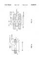
- FIG. 1ashows in plan view a typical prior art load resistor for use in a static RAM cell.
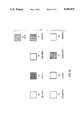
- FIG. 1bshows in plan view the load resistor of this invention.
- FIG. 2shows a circuit schematic of a single CMOS SRAM cell utilizing the load resistor of this invention.
- FIG. 3a-3killustrate a number of intermediate forms of the structure of this invention during various stages of the manufacture of the load resistor of this invention.
- FIGS. 4a and 4billustrate in plan view the compact nature of four CMOS SRAM cells utilizing the load resistor of this invention.
- FIG. 4cillustrates which type of materials are indicated by which type of shading in FIGS. 4a and 4b.
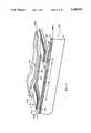
- FIGS. 5 and 6show an isometric cut-away view of the load resistor structure of this invention.
- FIG. 1aillustrates the conventional prior art static RAM load resistor structure formed using doped polycrystalline silicon.
- a polysilicon strip 1is formed on a semiconductor substrate and then a mask 2 (typically photoresist) is formed over the portion 1c of polycrystalline silicon strip 1 to comprise the load resistor Mask 2 is defined such that edges 2a and 2b define respectively the initial left and right limits of the to-be-formed load resistor 1c.
- mask 2is defined such that edges 2a and 2b define respectively the initial left and right limits of the to-be-formed load resistor 1c.
- dopantis placed in regions 1a and 1b of the polycrystalline silicon 1 in a well-known manner, typically by ion. implantation.
- FIG. 1aillustrates the conventional prior art static RAM load resistor structure formed using doped polycrystalline silicon.
- the load resistor according to this inventionillustrated in FIG. 1b overcomes this problem.
- two conductive strips 101 and 102typically titanium silicide, are formed on an insulating layer which in turn is formed on an underlying semiconductor substrate.
- Strips 101 and 102are either totally silicide or a top layer of silicide overlying a bottom layer of polycrystalline silicon.
- Over the silicide 101, 102are formed a titanium nitride layer and an oxide layer.
- vias 101a and 102aare formed in the oxide to selectively expose portions of the titanium nitride on the underlying silicide strips 101 and 102.
- oxidecan be formed directly over silicide 101, 102 without the intervening layer of titanium nitride.
- the titanium nitride capis selectively formed on those portions of silicide 101, 102 exposed by vias 101a and 102a.
- a layer of polycrystalline silicon 103is then deposited over the vias 101a and 102a so as to contact the titanium nitride exposed by or formed in these vias as well as over the oxide between these two vias so as to extend between these two vias over the region 105 between strip 101 and strip 102.
- This layer of polycrystalline silicon 103can in fact overlap portions of the underlying silicide and oxide sandwich outside of vias 101a and 102a, as shown by the annular band of material 103a surrounding alternative via 104.
- Alternate via 104removes a thin layer of the thicker oxide over the semiconductor substrate between vias 101a and 102a as well as the oxide over vias 101a and 102a.
- polycrystalline silicon 103Electrical contact to polycrystalline silicon 103 is made from silicide strips 101 and 102 (typically titanium silicide) through the electrically conductive titanium nitride formed over the top surface of strips 101 and 102.
- Polycrystalline silicon 103contacts this titanium nitride in vias 101a and 102a respectively.
- the portion of polycrystalline silicon layer 103 extending across the distance 105 on the oxide formed on the wafer between silicide strips 101 and 102has a length d which remains constant despite further high temperature processing of the wafer.
- the titanium nitride in vias 101a and 102ais electrically conductive but serves as a barrier to the diffusion of impurities in strips 101 and 102 from these strips into polycrystalline silicon 103.
- the resistance of the load resistor 106is given by the length d, the width W and the thickness (not shown in FIG. 1b) of polycrystalline silicon 103.
- the length d of this resistorremains constant despite subsequent high temperature processing of the wafer. Accordingly, a load resistor is provided which has a resistance which is predictable and reproducible and which is controlled by the distance d representing the pitch between silicide strips 101 and 102.
- Distance dcan be as short as is feasible using semiconductor processing techniques and thus typically will be one micron or less in highly dense circuits. Tests have shown that the distance d can be as little as 0.9 microns and still yield a satisfactory load resistance. However, sufficient tests have not been run to determine the bottom limit on distance d and thus it is not known at this time the minimum value of distance d which will still yield a satisfactory load resistor in accordance with the teachings of this invention.
- FIG. 2illustrates a circuit schematic of a static RAM cell utilizing the load resistors R L1 and R L2 fabricated in accordance with this invention.
- transistor T2if on, results in the voltage on node A being at approximately ground while the voltage on node B is approximately at Vcc.
- the current through R L2should be nano-amps if R L2 is a high value such as 100 giga-ohms (corresponding to 100 ⁇ 109 ohms). If the voltage on node A is low, this low voltage is detected at B1 when pass transistor T4 is turned on in a well-known manner by applying a high level signal to the word line WL. If T1 is conducting, then the voltage on node B is low, that is approximately at ground. Transistor T2 is OFF because the voltage on node B is low and the voltage on node A must then be high.
- the method of forming a MOS field effect transistor of a CMOS integrated circuitbegins using well-known techniques to form N and P wells 10, and field and gate oxidation areas 11 and 12 respectively on doped silicon substrate 13.
- Gate oxide 12is typically 180 ⁇ thick.
- a layer 14 of polysilicon about 3000 ⁇ thickis formed by low pressure chemical vapor deposition (LPCVD) and doped typically by ion implantation can also be used, with N-type impurities to achieve a suitable sheet resistance, typically 50 ohms per square.
- the doped polysiliconwill function as a gate in the complete MOSFET device.
- First level interconnects, (not shown) usually located in the periphery of a memory array,can also be formed from this layer of polysilicon.
- a thin, 150 ⁇ oxide layer 15is thermally grown on the polysilicon.
- a layer 16 of silicon nitride about 1800 ⁇ thickis next formed on oxide layer 15 by LPCVD.
- the polysilicon gates 14a, 14bare defined by well-known photo-masking and sandwich etching techniques.
- the sandwich etchis carried out in a LAM 490.
- the anisotropic sandwich etchincludes a SF 6 plasma etch of the silicon nitride layer 16 and silicon oxide layer 15 and a subsequent anisotropic Cl 2 /He plasma etch of the polysilicon to form polysilicon gates 14a and 14b covered by layers 15a, 15b and 16a, 16b.
- LDD implants 17a, 17b, 17c, 17dWell known ion implantation techniques are next used to 12 form both N- and P- type lightly doped drain (LDD) implants 17a, 17b, 17c, 17d (FIG. 3d) so that the LDD implants have a conductivity type that is opposite to that of the well 10 or the substrate 13 if no well is present.
- the impurity concentration of the LDD implantsis about 1.8 ⁇ 10 13 dopant atoms per cubic centimeter.
- gate sidewall spacers 18a, 18b, 18c, 18d of silicon dioxidewhich are approximately 4000-4200 ⁇ thick.
- a layer of oxide 100 ⁇ thick(not shown) is thermally grown at approximately 800° C. to cap the source and drain regions and to densify the spacer oxide 18a-18d.
- N+and P+type source and drain regions 19a, 19b, 19c, 19dare then formed by well known masked ion implantation so that the dopant concentration is typically 3 ⁇ 10 15 -5 ⁇ 10 15 dopant atoms per cubic centimeter in these regions.
- Gate contact regionsare defined as described below. Referring to FIG. 3e, chemical vapor deposition of a silicon oxide layer 20, 1100 ⁇ thick, is followed by annealing of the layer at 875° C. for 30 minutes in a nitrogen atmosphere.
- the waferis then coated with a standard Novolak based positive photoresist available from Shipley which tends to planarize the wafer, and is then baked.
- the photoresist 21is blanket etched by oxygen plasma in plasma etcher AME 8115 until the oxide 20 covering the gate region is visible.
- a second bake of resist layer 21 at 150° C. for approximately 30 minuteshardens the resist 21 and makes it unreactive in subsequent steps.
- an openingis formed through oxide 20, nitride 16b and oxide 15b to allow electrical contact to be made to gate 14b.
- the polysilicon isolation mask used for this purpose to expose the gate 14bcan have a contact size extending beyond the gate, thereby permitting a looser alignment tolerance.
- An approximation of the variable position of the contact opening to gate 14b due to alignment tolerances for the maskis shown by the dashed lines in FIG. 3f.
- the presence of the first photoresis 21prevents exposure of the source and drain regions 19c,d during etching of the oxide layers 20 and 15b and silicon nitride layer 16b to expose the gate 14a, even in the event of worst case alignment of the mask. In this way electrical contact to the gate 14b can be made over, the active channel region of the transistor under gate 14b without causing a short circuit between the source or drain 19c,d and the gate 14b.
- a multi-step etchis conducted to expose the gate contact.
- the oxide 20is removed in the area exposed by the opening 22a in resist layer 22 with a dry plasma etch using C 2 F 6 /CHF 3 in a 25:12 ratio.
- 1200-1500 ⁇ of the silicon nitride layer 16bis removed by a CF 4 plasma etch.
- CF 4etches all exposed materials at approximately the same rate to help create a smooth profile above gate 14b and causes a step in the oxide 18c, 18d at the interface of the oxide 18c, 18d and the first layer 21 of photoresist.
- both photoresist layers 21, 22is followed by a standard wet phosphoric acid etch with a 50 to 1 selectivity toward silicon oxide which (i.e., phosphoric acid etches silicon nitride fifty times more rapidly than silicon oxide) which removes the remainder of nitride layer 16b.
- a blanket CF 4 plasma etchremoves 150 ⁇ thick oxide layer 15b and decreases the height of the oxide step in oxide 18c, 18d on the sides of gate 14b to produce the polysilicon gate contact 14c shown in FIG. 3g.
- a process using only dry etchants for exposing the gate contactis also feasible.
- contacts to the source and drain C 2 F 6 /CHF 3 plasma etch of the oxide 20removes only 10 to 20% of spacer oxide 18a, 18b because spacer oxide 18a, 18b is significantly thicker than oxide 20.
- the silicon nitride layer 16aprotects the gate 14a after some portion of the oxide 20 covering the gate is removed. With spacer oxide 18a, 18b and protective silicon nitride layer 16a intact on gate 14a, source and drain contact metallization deposited later can overlap the gate without causing a short circuit between the source and drain 19b and the gate 14a.
- the plasma oxide etchis followed by a backside etch which exposes pure silicon on the back side of the substrate 10. This exposure allows the temperature of the substrate 10 to be more closely monitored and controlled in subsequent processing steps.
- the backside etchis conducted in three steps. The first step using a 12:8 ratio of CHF 3 /SF 6 in helium is followed by a second step using only SF 6 in : helium. The third step uses 20:8 CHF 3 /SF 6 also in helium.
- the silicon exposed by the source, drain and polysilicon gate contacts and the interconnectsare silicided by depositing a layer of sputtered titanium about 700 ⁇ thick and using rapid thermal annealing at 700° C. in a N 2 atmosphere to form a layer of TiSi coated by a thin layer of titanium nitride.
- the rapid thermal annealing processinvolves quickly heating the substrate to a predetermined temperature, holding the substrate at that temperature for 30 seconds and then returning it to its original temperature. The substrate can reach the predetermined temperature as quickly as 15 seconds
- the rapid thermal model ALP-5500The rapid thermal model ALP-5500.
- the unreacted titaniumis stripped from the substrate's surface with a 5:1:1 solution of water, hydrogen peroxide and ammonium hydroxide which also attacks and removes the titanium nitride layer.
- a second rapid thermal annealing step at 900° C. for 30 seconds in an atmosphere of ammoniaconverts the TiSi to the stable silicide TiSi 2 layer 23a, 23b, coated by a thin layer of titanium nitride (not shown). In this way, areas of titanium silicide are selectively formed. For instance, the gate is silicided only at regions which will contact the subsequently formed local interconnects because these are the only gate regions exposed by previous processing steps.
- the silicided layer 23a, 23bcan protect the underlying source, drain and gate regions and the interconnects during later processing steps, particularly the formation of local interconnects to be formed from a second polysilicon layer.
- Local interconnectsare formed from a second layer of polysilicon about 700 ⁇ thick which is deposited by LPCVD in a well-known manner. However, before the wafers are inserted into the reactor, the reactor temperature is lowered to 150° C. The reactor chamber is evacuated and backfilled with an inert gas before the temperature is raised so as to lessen the wafers contact with oxygen at high temperatures. Well-known masking and etching processes define the local interconnects. Use of an isotropic SF 6 /O 2 plasma etch diminishes the necessity of overetch.
- the etchis selective to titanium silicide, the underlying titanium silicide layer 23a, 23b prevents damage to the source, drain and gate contacts and the first layer interconnects formed from the first polysilicon layer during the etch, therefore, the local interconnects are not required to completely overlap these regions.
- Layer 23also acts as an etch stop so that the etchant will not remove the polysilicon gate or first layer interconnects during overetching of the local interconnects.
- a 500 ⁇ layer of sputtered titaniumis deposited on the substrate. Rapid thermal annealing at 640° C. in a nitrogen atmosphere for 60 seconds forms titanium silicide TiSi x local interconnects 27 encapsulated by a thin titanium nitride film. The unreacted titanium and the titanium nitride film are stripped from the surface with a solution of 5:1:1 water, hydrogen peroxide and ammonium hydroxide to give the structure shown in FIG. 3i.
- a 500 ⁇ thick layer of oxideis deposited from a mixture of silane, nitrous oxide and nitrogen at approximately 400° C. to act as an isolation layer 29.
- Masking and a standard CHF 3 /O 2 plasma oxide etchare used to open load resistor vias 30 to selected regions of local interconnects 27. Rapid thermal annealing at 850° C. for 30 seconds in a nitrogen atmosphere converts the TiSi x of the local interconnects to TiSi 2 to create low resistance interconnects.
- a thin titanium nitride film 28forms on the regions of the local interconnects exposed by vias 30. Titanium nitride is a good electrical conductor but a barrier to dopant diffusion. This barrier will prevent dopants from diffusing into the polysilicon resistors formed by subsequent processing steps.
- a layer 32 of oxide 1200-1500 ⁇ thickis deposited from a mixture of silane, nitrous oxide and nitrogen at approximately 400° C.
- a doped boron-phosphorous glass 33which acts as an insulation layer is deposited over oxide 32 in a manner similar to oxide 32 but with the addition of diborane and phosphine to the starting gases. The glass 33 is flowed at 800° C. for 30 minutes to form a more level surface.
- Oxide layer 32prevents diffusion of boron and phosphorus from boron-phosphorus glass 33 to resistors 31.
- FIGS. 4a and 4bshow the layout of a four cell CMOS 100 SRAM memory using this invention.
- a key illustrating which materials are symbolized by which shading typesis also provided as FIG. 4c.
- FIG. 4awhich shows only some of the cell components for clarity, each cell occupies one quadrant as divided along lines A--A and B--B.
- Reference numbers 40 and 42indicate the field oxide and the island or active area, respectively.
- the two conductive gates 44 per cellare formed from the first deposited layer of polysilicon. Contacts 46 to the polysilicon gates 44 can be wider than the gates 44 themselves as indicated by the hash lines 46a.
- Buried contacts 48 open to the source and drain regionscan overlap but not electrically and ohmically contact gate 44 by the process described above.
- each buried contact 48is electrically connected to a gate contact 46 via a conductive titanium silicide local interconnect structure 50.
- Other components of each cellinclude the bit line contact 52, the polysilicon word line 54, the silicided V cc 56 and the silicided ground
- Load resistor vias 60are located above a buried contact 48 and overlap a gate contact 46 as indicated by the hash lines 60a.
- the location of the load resistors 62is indicated by a heavy line.
- a via 64 to the V cc line 56is opened between two cells.
- Vertical heavy line 66 and horizontal stripes of shading 68show the location of connective metal lines formed by standard techniques.
- shading 70indicates titanium silicide layers.
- Shading 71indicates an island region.
- Shading 72shows cell components formed of polysilicon by the first deposition of polysilicon.
- Hash lines 73outline the borders of the polyisolation mask which open the gate contact.
- Shading 74indicates bit contacts.
- Hash lines 75outline load resistor vias.
- Heavy lines 76outline load resistors.
- Shading 77indicates a contact region.
- Light lines 78show metallic interconnects. Field oxide in FIGS. 4a and 4b is not shown with shading or outlines but occupies the white, unmarked portions of the cell layout.
- FIG. 5Shown in FIG. 5 is an isometric view of one load resistor structure made in accordance with the invention.
- a portion 100 of a semiconductor substratehas formed on it a layer of silicon dioxide 100a.
- Formed on top of the oxide 100aare two silicide strips 101 and 102. These strips are separated as shown by the distance d.
- Formed on the top surfaces of titanium silicide strips 101 and 102are sandwiches of titanium nitride 101b, 102b and silicon oxide 101c, 102c.
- the structure shown in FIG. 5illustrates silicide strips 101 and 102 formed by completely converting two polycrystalline silicon strips into a selected silicide covered by a nitride, preferably titanium silicide and titanium nitride.
- strips 101 and 102can alternatively comprise a composite of polycrystalline silicon overlain by a selected silicide such as titanium silicide and titanium nitride can be formed only on those portions of the strips exposed by vias 101a and 102a.
- a titanium silicide layer 111ais formed from the top portion of polycrystalline silicon strip 111 by placing titanium on top of strip 111 and heating the wafer to approximately 900° C. in a nitrogen or ammonia atmosphere. As a result of this heating, a layer of titanium nitride 111b is formed on the titanium silicide 111a formed from the top portion of polycrystalline silicon strip 111.
- a titanium silicide layer 112ais formed from the top portion of polycrystalline silicon 112 and a titanium nitride layer 112b is formed on top of titanium silicide layer 112a during the heating of the wafer in the same nitrogen or ammonia atmosphere to form the titanium silicide.
- the titanium nitride layer 111b, 112bforms an excellent electrical conductor, but at the same time forms a barrier to the diffusion of the impurities or dopants within strips 111 and 112.
- a layer of oxide 111c and 112cis formed on the titanium nitride 111b and 112b and oxide 107 (not shown) is formed on the oxide 100a which has previously been formed on semiconductor substrate 100.
- the oxide layer 111c, 112cis then etched to form vias (corresponding to vias 101a and 102a in FIG. 1b) and a polycrystalline silicon sheet 103 is deposited over the surface of the wafer.
- one via 104can be etched through oxide 111c, 112c and 107.
- the portions of polycrystalline silicon sheet 103 which contact the titanium nitride 111b and 112b through the vias 101a and 102a (FIG. 1b) or through via 104 (also FIG. 1b)provide the conductive contacts to the ends of the resistive structure to be formed from polysilicon 103.
- the polycrystalline silicon 103is then masked with a photoresist 106 to leave photoresist over only that portion of the polycrystalline silicon layer 103 to be retained as the high resistance load resistor structure.
- polycrystalline silicon layer 103is then removed, typically by a dry etch. Then the remaining polycrystalline silicon layer 103 functions as the high resistance load resistor.
- This layer 103has a thickness t, a length d and a width w which determine the resistance of this structure.
- the resistance of polycrystalline silicon layer 103can vary over a wide range, typically from 10 giga-ohms to several hundred giga-ohms, and not materially affect the operation of the circuit. While the current which flows through the load resistor 103 formed from polycrystalline silicon 103 will increase directly as the resistance of this load resistor decreases, the currents which are typically drawn through this load resistor are in the pico-amp range. Thus the total current through a 256K memory cell utilizing the load resistor of this invention is still in the microamp range in the worst case, an acceptable current range for this kind of product.
- the resistance of the load resistor of this inventionis in the giga-ohms range at room temperature, as the resistor heats up, its resistance drops.
- a resistor which has a value of 100 giga-ohms at room temperaturecan drop to 10 giga-ohms at the maximum operating temperature of the circuit thereby resulting in a 10 times current increase.
- the current through a static RAM using the load resistance of this inventioncan be in the microamp range or even in the milliamp ramp depending upon the specifications of the product and the application to which the product is put.
- This inventionalso allows for load resistors having resistance values above 100 giga-ohms. These high resistance values make possible the fabrication of static random access memory cells with very low stand-by currents.
- the titanium nitride layers 111b and 112bprovide a barrier to the diffusion of dopants from underlying strips 111 and 112 into polycrystalline silicon regions 103a and 103b.
- titanium nitride layers 111b and 112bare electrically conductive and thus allow the load resistor 103 to be electrically contacted through strips 111 and 112.
- a particular advantage of this inventionis that as the distance d becomes less than one micron the resistance of polycrystalline silicon material 103 can be satisfactorily controlled even should the wafer be subjected to subsequent high temperature processing steps.
- the dopant barriercomprising titanium nitride 111b, 112b overlying titanium silicide 111a, 112a in the vias though which the ends 103a, 103b of the load resistor 103 ohmically contact the underlying conductive regions 111, 112 can be locally formed after the vias 101a, 102a are formed rather than formed prior to the deposition of oxide 111c, 112 and the formation of these vias.
Landscapes
- Semiconductor Memories (AREA)
- Internal Circuitry In Semiconductor Integrated Circuit Devices (AREA)
Abstract
Description
Claims (7)
Priority Applications (1)
| Application Number | Priority Date | Filing Date | Title |
|---|---|---|---|
| US07/724,008US5168076A (en) | 1990-01-12 | 1991-07-01 | Method of fabricating a high resistance polysilicon load resistor |
Applications Claiming Priority (2)
| Application Number | Priority Date | Filing Date | Title |
|---|---|---|---|
| US07/464,094US5172211A (en) | 1990-01-12 | 1990-01-12 | High resistance polysilicon load resistor |
| US07/724,008US5168076A (en) | 1990-01-12 | 1991-07-01 | Method of fabricating a high resistance polysilicon load resistor |
Related Parent Applications (1)
| Application Number | Title | Priority Date | Filing Date |
|---|---|---|---|
| US07/464,094DivisionUS5172211A (en) | 1990-01-12 | 1990-01-12 | High resistance polysilicon load resistor |
Publications (1)
| Publication Number | Publication Date |
|---|---|
| US5168076Atrue US5168076A (en) | 1992-12-01 |
Family
ID=27040840
Family Applications (1)
| Application Number | Title | Priority Date | Filing Date |
|---|---|---|---|
| US07/724,008Expired - Fee RelatedUS5168076A (en) | 1990-01-12 | 1991-07-01 | Method of fabricating a high resistance polysilicon load resistor |
Country Status (1)
| Country | Link |
|---|---|
| US (1) | US5168076A (en) |
Cited By (25)
| Publication number | Priority date | Publication date | Assignee | Title |
|---|---|---|---|---|
| US5232863A (en)* | 1992-10-20 | 1993-08-03 | Micron Semiconductor, Inc. | Method of forming electrical contact between a field effect transistor gate and a remote active area |
| US5244826A (en)* | 1992-04-16 | 1993-09-14 | Micron Technology, Inc. | Method of forming an array of finned memory cell capacitors on a semiconductor substrate |
| US5349325A (en)* | 1993-05-18 | 1994-09-20 | Integrated Device Technology, Inc. | Multi-layer low modulation polycrystalline semiconductor resistor |
| US5433794A (en)* | 1992-12-10 | 1995-07-18 | Micron Technology, Inc. | Spacers used to form isolation trenches with improved corners |
| US5470780A (en)* | 1993-09-16 | 1995-11-28 | Nec Corporation | Method of fabricating poly-silicon resistor |
| US5521117A (en)* | 1993-11-01 | 1996-05-28 | Lsi Logic Corporation | Process for active device constructed in opening formed in insulation layer with a resistor |
| US5589417A (en)* | 1993-01-12 | 1996-12-31 | Texas Instruments, Incorporated | TiSi2 /TiN clad interconnect technology |
| US5652174A (en)* | 1996-05-20 | 1997-07-29 | Taiwan Semiconductor Manufacturing Company Ltd. | Unified stacked contact process for static random access memory (SRAM) having polysilicon load resistors |
| US5668037A (en)* | 1995-10-06 | 1997-09-16 | Micron Technology, Inc. | Method of forming a resistor and integrated circuitry having a resistor construction |
| US5780331A (en)* | 1997-01-15 | 1998-07-14 | Taiwan Semiconductor Manufacturing Company Ltd. | Method of making buried contact structure for a MOSFET device in an SRAM cell |
| US5849629A (en)* | 1995-10-31 | 1998-12-15 | International Business Machines Corporation | Method of forming a low stress polycide conductors on a semiconductor chip |
| US5872030A (en)* | 1997-10-27 | 1999-02-16 | Taiwan Semiconductor Manufacturing Company, Ltd. | Method of improving beta ratio in SRAM and device manufactured thereby |
| US5923078A (en)* | 1996-07-11 | 1999-07-13 | Micron Technology, Inc. | Method of forming a resistor and integrated circuitry having a resistor construction |
| US5936306A (en)* | 1993-01-12 | 1999-08-10 | Texas Instruments Incorporated | TiSi2 /TiN clad interconnect technology |
| US5952246A (en)* | 1993-11-03 | 1999-09-14 | Advanced Micro Devices, Inc. | Nitride selective, anisotropic Cl2 /He etch process |
| US5977598A (en)* | 1997-09-23 | 1999-11-02 | Winbond Electronics Corporation | High load resistance implemented in a separate polysilicon layer with diffusion barrier therein for preventing load punch through therefrom |
| US5985768A (en)* | 1997-04-30 | 1999-11-16 | International Business Machines Corporation | Method of forming a semiconductor |
| US6127217A (en)* | 1998-05-28 | 2000-10-03 | Altera Corporation | Method of forming highly resistive interconnects |
| US6130137A (en)* | 1997-10-20 | 2000-10-10 | Micron Technology, Inc. | Method of forming a resistor and integrated circuitry having a resistor construction |
| US6143613A (en)* | 1997-06-30 | 2000-11-07 | Vlsi Technology, Inc. | Selective exclusion of silicide formation to make polysilicon resistors |
| US6147406A (en)* | 1996-08-20 | 2000-11-14 | Micron Technology, Inc. | Electrical connection between an electrically conductive line and a node location, and integrated circuitry |
| US6165861A (en)* | 1998-09-14 | 2000-12-26 | Taiwan Semiconductor Manufacturing Company | Integrated circuit polysilicon resistor having a silicide extension to achieve 100% metal shielding from hydrogen intrusion |
| US6165831A (en)* | 1998-11-20 | 2000-12-26 | United Microelectronics Corp. | Method of fabricating a buried contact in a static random access memory |
| US6207543B1 (en) | 1997-06-30 | 2001-03-27 | Vlsi Technology, Inc. | Metallization technique for gate electrodes and local interconnects |
| US8803243B2 (en) | 2012-01-03 | 2014-08-12 | International Business Machines Corporation | Complementary metal oxide semiconductor (CMOS) device having gate structures connected by a metal gate conductor |
Citations (10)
| Publication number | Priority date | Publication date | Assignee | Title |
|---|---|---|---|---|
| US4329706A (en)* | 1979-03-01 | 1982-05-11 | International Business Machines Corporation | Doped polysilicon silicide semiconductor integrated circuit interconnections |
| EP0173245A1 (en)* | 1984-08-23 | 1986-03-05 | Kabushiki Kaisha Toshiba | Semiconductor memory device having a polycrystalline silicon layer |
| JPS62290164A (en)* | 1986-06-09 | 1987-12-17 | Oki Electric Ind Co Ltd | Formation of semiconductor element |
| JPS62290166A (en)* | 1986-06-09 | 1987-12-17 | Oki Electric Ind Co Ltd | Manufacture of semiconductor element |
| US4774203A (en)* | 1985-10-25 | 1988-09-27 | Hitachi, Ltd. | Method for making static random-access memory device |
| US4835118A (en)* | 1986-09-08 | 1989-05-30 | Inmos Corporation | Non-destructive energy beam activated conductive links |
| US4931411A (en)* | 1985-05-01 | 1990-06-05 | Texas Instruments Incorporated | Integrated circuit process with TiN-gate transistor |
| US5013686A (en)* | 1987-09-30 | 1991-05-07 | Samsung Electronics Co., Ltd. | Method of making semiconductor devices having ohmic contact |
| US5013678A (en)* | 1986-11-18 | 1991-05-07 | Siemens Aktiengesellschaft | Method of making an integrated circuit comprising load resistors arranged on the field oxide zones which separate the active transistor zones |
| US5037766A (en)* | 1988-12-06 | 1991-08-06 | Industrial Technology Research Institute | Method of fabricating a thin film polysilicon thin film transistor or resistor |
- 1991
- 1991-07-01USUS07/724,008patent/US5168076A/ennot_activeExpired - Fee Related
Patent Citations (11)
| Publication number | Priority date | Publication date | Assignee | Title |
|---|---|---|---|---|
| US4329706A (en)* | 1979-03-01 | 1982-05-11 | International Business Machines Corporation | Doped polysilicon silicide semiconductor integrated circuit interconnections |
| EP0173245A1 (en)* | 1984-08-23 | 1986-03-05 | Kabushiki Kaisha Toshiba | Semiconductor memory device having a polycrystalline silicon layer |
| US4903096A (en)* | 1984-08-23 | 1990-02-20 | Kabushiki Kaisha Toshiba | Semiconductor memory device with barrier layer |
| US4931411A (en)* | 1985-05-01 | 1990-06-05 | Texas Instruments Incorporated | Integrated circuit process with TiN-gate transistor |
| US4774203A (en)* | 1985-10-25 | 1988-09-27 | Hitachi, Ltd. | Method for making static random-access memory device |
| JPS62290164A (en)* | 1986-06-09 | 1987-12-17 | Oki Electric Ind Co Ltd | Formation of semiconductor element |
| JPS62290166A (en)* | 1986-06-09 | 1987-12-17 | Oki Electric Ind Co Ltd | Manufacture of semiconductor element |
| US4835118A (en)* | 1986-09-08 | 1989-05-30 | Inmos Corporation | Non-destructive energy beam activated conductive links |
| US5013678A (en)* | 1986-11-18 | 1991-05-07 | Siemens Aktiengesellschaft | Method of making an integrated circuit comprising load resistors arranged on the field oxide zones which separate the active transistor zones |
| US5013686A (en)* | 1987-09-30 | 1991-05-07 | Samsung Electronics Co., Ltd. | Method of making semiconductor devices having ohmic contact |
| US5037766A (en)* | 1988-12-06 | 1991-08-06 | Industrial Technology Research Institute | Method of fabricating a thin film polysilicon thin film transistor or resistor |
Non-Patent Citations (8)
| Title |
|---|
| IEEE Transactions on Electron Devices, vol. 35, No. 3, Mar. 1988, pp. 298 301; R. Saito et al. entitled A Novel Scaled Down Oxygen Implanted . . . .* |
| IEEE Transactions on Electron Devices, vol. 35, No. 3, Mar. 1988, pp. 298-301; R. Saito et al. entitled "A Novel Scaled-Down Oxygen-Implanted . . .". |
| IEEE Transactions on Electron Devices, vol. 36, No. 9, Sep. 1989, pp. 1657 1662; M. Minami et al. entitled A New Soft Error Immune Static . . . .* |
| IEEE Transactions on Electron Devices, vol. 36, No. 9, Sep. 1989, pp. 1657-1662; M. Minami et al. entitled "A New Soft-Error-Immune Static . . .". |
| IEEE VLSI Multilevel Interconnection Conference, Jun. 1986, pp. 530 536; N. McIntyre et al. entitled Self Aligned Silicide Interconnection . . . .* |
| IEEE VLSI Multilevel Interconnection Conference, Jun. 1986, pp. 530-536; N. McIntyre et al. entitled "Self Aligned Silicide Interconnection . . .". |
| Journal of Vacuum Science and Technology: Part A, No. 4, 1987, pp. 2184 2189; E. O. Ristolainen et al. entitled A Study of Nitrogen Rich . . . .* |
| Journal of Vacuum Science and Technology: Part A, No. 4, 1987, pp. 2184-2189; E. O. Ristolainen et al. entitled "A Study of Nitrogen-Rich . . .". |
Cited By (36)
| Publication number | Priority date | Publication date | Assignee | Title |
|---|---|---|---|---|
| US5244826A (en)* | 1992-04-16 | 1993-09-14 | Micron Technology, Inc. | Method of forming an array of finned memory cell capacitors on a semiconductor substrate |
| US5232863A (en)* | 1992-10-20 | 1993-08-03 | Micron Semiconductor, Inc. | Method of forming electrical contact between a field effect transistor gate and a remote active area |
| US5868870A (en)* | 1992-12-10 | 1999-02-09 | Micron Technology, Inc. | Isolation structure of a shallow semiconductor device trench |
| US5433794A (en)* | 1992-12-10 | 1995-07-18 | Micron Technology, Inc. | Spacers used to form isolation trenches with improved corners |
| US5966615A (en)* | 1992-12-10 | 1999-10-12 | Micron Technology, Inc. | Method of trench isolation using spacers to form isolation trenches with protected corners |
| US5733383A (en)* | 1992-12-10 | 1998-03-31 | Micron Technology, Inc. | Spacers used to form isolation trenches with improved corners |
| US5589417A (en)* | 1993-01-12 | 1996-12-31 | Texas Instruments, Incorporated | TiSi2 /TiN clad interconnect technology |
| US5936306A (en)* | 1993-01-12 | 1999-08-10 | Texas Instruments Incorporated | TiSi2 /TiN clad interconnect technology |
| US5349325A (en)* | 1993-05-18 | 1994-09-20 | Integrated Device Technology, Inc. | Multi-layer low modulation polycrystalline semiconductor resistor |
| US5470780A (en)* | 1993-09-16 | 1995-11-28 | Nec Corporation | Method of fabricating poly-silicon resistor |
| US5521117A (en)* | 1993-11-01 | 1996-05-28 | Lsi Logic Corporation | Process for active device constructed in opening formed in insulation layer with a resistor |
| US5952246A (en)* | 1993-11-03 | 1999-09-14 | Advanced Micro Devices, Inc. | Nitride selective, anisotropic Cl2 /He etch process |
| US5940712A (en)* | 1995-10-06 | 1999-08-17 | Micron Technology, Inc. | Method of forming a resistor and integrated circuitry having a resistor construction |
| US5821150A (en)* | 1995-10-06 | 1998-10-13 | Micron Technology, Inc. | Method of forming a resistor and integrated circuitry having a resistor construction |
| US5780920A (en)* | 1995-10-06 | 1998-07-14 | Micron Technology, Inc. | Method of forming a resistor and integrated circuitry having a resistor construction |
| US5668037A (en)* | 1995-10-06 | 1997-09-16 | Micron Technology, Inc. | Method of forming a resistor and integrated circuitry having a resistor construction |
| US5849629A (en)* | 1995-10-31 | 1998-12-15 | International Business Machines Corporation | Method of forming a low stress polycide conductors on a semiconductor chip |
| US5652174A (en)* | 1996-05-20 | 1997-07-29 | Taiwan Semiconductor Manufacturing Company Ltd. | Unified stacked contact process for static random access memory (SRAM) having polysilicon load resistors |
| US5923078A (en)* | 1996-07-11 | 1999-07-13 | Micron Technology, Inc. | Method of forming a resistor and integrated circuitry having a resistor construction |
| US6261940B1 (en)* | 1996-08-20 | 2001-07-17 | Micron Technology, Inc. | Semiconductor method of making electrical connection between an electrically conductive line and a node location, and integrated circuitry |
| US6351038B1 (en) | 1996-08-20 | 2002-02-26 | Micron Technology, Inc. | Integrated circuitry |
| US6583042B2 (en) | 1996-08-20 | 2003-06-24 | Micron Technology, Inc. | Semiconductor method of making electrical connection between an electrically conductive line and a node location, and integrated circuitry |
| US6147406A (en)* | 1996-08-20 | 2000-11-14 | Micron Technology, Inc. | Electrical connection between an electrically conductive line and a node location, and integrated circuitry |
| US5780331A (en)* | 1997-01-15 | 1998-07-14 | Taiwan Semiconductor Manufacturing Company Ltd. | Method of making buried contact structure for a MOSFET device in an SRAM cell |
| US5985768A (en)* | 1997-04-30 | 1999-11-16 | International Business Machines Corporation | Method of forming a semiconductor |
| US6143613A (en)* | 1997-06-30 | 2000-11-07 | Vlsi Technology, Inc. | Selective exclusion of silicide formation to make polysilicon resistors |
| US6207543B1 (en) | 1997-06-30 | 2001-03-27 | Vlsi Technology, Inc. | Metallization technique for gate electrodes and local interconnects |
| US5977598A (en)* | 1997-09-23 | 1999-11-02 | Winbond Electronics Corporation | High load resistance implemented in a separate polysilicon layer with diffusion barrier therein for preventing load punch through therefrom |
| US6130137A (en)* | 1997-10-20 | 2000-10-10 | Micron Technology, Inc. | Method of forming a resistor and integrated circuitry having a resistor construction |
| US5872030A (en)* | 1997-10-27 | 1999-02-16 | Taiwan Semiconductor Manufacturing Company, Ltd. | Method of improving beta ratio in SRAM and device manufactured thereby |
| US6127217A (en)* | 1998-05-28 | 2000-10-03 | Altera Corporation | Method of forming highly resistive interconnects |
| US6340833B1 (en) | 1998-09-14 | 2002-01-22 | Taiwan Semiconductor Manufacturing Company | Integrated circuit polysilicon resistor having a silicide extension to achieve 100 % metal shielding from hydrogen intrusion |
| US6165861A (en)* | 1998-09-14 | 2000-12-26 | Taiwan Semiconductor Manufacturing Company | Integrated circuit polysilicon resistor having a silicide extension to achieve 100% metal shielding from hydrogen intrusion |
| US6165831A (en)* | 1998-11-20 | 2000-12-26 | United Microelectronics Corp. | Method of fabricating a buried contact in a static random access memory |
| US8803243B2 (en) | 2012-01-03 | 2014-08-12 | International Business Machines Corporation | Complementary metal oxide semiconductor (CMOS) device having gate structures connected by a metal gate conductor |
| US9082877B2 (en) | 2012-01-03 | 2015-07-14 | International Business Machines Corporation | Complementary metal oxide semiconductor (CMOS) device having gate structures connected by a metal gate conductor |
Similar Documents
| Publication | Publication Date | Title |
|---|---|---|
| US5168076A (en) | Method of fabricating a high resistance polysilicon load resistor | |
| US5172211A (en) | High resistance polysilicon load resistor | |
| US5620919A (en) | Methods for fabricating integrated circuits including openings to transistor regions | |
| US5483104A (en) | Self-aligning contact and interconnect structure | |
| US5027185A (en) | Polycide gate FET with salicide | |
| US5998252A (en) | Method of salicide and sac (self-aligned contact) integration | |
| US4821085A (en) | VLSI local interconnect structure | |
| US5334862A (en) | Thin film transistor (TFT) loads formed in recessed plugs | |
| US6583005B2 (en) | Method of manufacturing a semiconductor memory device with a buried bit line | |
| US5874353A (en) | Method of forming a self-aligned silicide device | |
| JPH09191112A (en) | Spacer type thin film polysilicon transistor for low power memory device | |
| US6333233B1 (en) | Semiconductor device with self-aligned contact and its manufacture | |
| US5911105A (en) | Flash memory manufacturing method | |
| JPS6249750B2 (en) | ||
| US6352891B1 (en) | Method of manufacturing semiconductor device in which hot carrier resistance can be improved and silicide layer can be formed with high reliability | |
| JP2585140B2 (en) | Wiring contact structure of semiconductor device | |
| US5795827A (en) | Method for reducing the resistance of self-aligned contacts, for triple polysilicon SRAM devices | |
| US5494848A (en) | Buried contact trench process | |
| US5654231A (en) | Method of eliminating buried contact trench in SRAM technology | |
| US7332811B2 (en) | Integrated circuit interconnect | |
| US6174762B1 (en) | Salicide device with borderless contact | |
| US5521416A (en) | Semiconductor device having gate electrode and impurity diffusion layer different in conductivity type and method of manufacturing the same | |
| US20010014530A1 (en) | Method for manufacturing a semiconductor device | |
| KR20030054778A (en) | Method for fabricating mask rom | |
| EP0534203B1 (en) | Semiconductor device |
Legal Events
| Date | Code | Title | Description |
|---|---|---|---|
| AS | Assignment | Owner name:NUF CORPORATION, NEW YORK Free format text:SECURITY INTEREST;ASSIGNOR:PARADIGM TECHNOLOGY, INC.;REEL/FRAME:006746/0802 Effective date:19930928 | |
| AS | Assignment | Owner name:CREDIT MANAGERS ASSOCIATION OF CALIFORNIA, CALIFOR Free format text:MEMORANDUM OF SECURITY INTEREST (WITH SECURITY AGREEMENT ATTACHED AS EXHIBIT);ASSIGNOR:PARADIGM TECHNOLOGY, INC.;REEL/FRAME:007114/0942 Effective date:19940805 | |
| FPAY | Fee payment | Year of fee payment:4 | |
| AS | Assignment | Owner name:GREYROCK BUSINESS CREDIT, A DIVISION OF NATIONSCRE Free format text:SECURITY INTEREST;ASSIGNOR:PARADIGM TECHNOLOGY, INC.;REEL/FRAME:008170/0755 Effective date:19961025 | |
| FEPP | Fee payment procedure | Free format text:PAT HOLDER CLAIMS SMALL ENTITY STATUS - SMALL BUSINESS (ORIGINAL EVENT CODE: SM02); ENTITY STATUS OF PATENT OWNER: SMALL ENTITY | |
| FPAY | Fee payment | Year of fee payment:8 | |
| FEPP | Fee payment procedure | Free format text:PAYOR NUMBER ASSIGNED (ORIGINAL EVENT CODE: ASPN); ENTITY STATUS OF PATENT OWNER: SMALL ENTITY Free format text:PAYER NUMBER DE-ASSIGNED (ORIGINAL EVENT CODE: RMPN); ENTITY STATUS OF PATENT OWNER: SMALL ENTITY | |
| REMI | Maintenance fee reminder mailed | ||
| LAPS | Lapse for failure to pay maintenance fees | ||
| LAPS | Lapse for failure to pay maintenance fees | Free format text:PATENT EXPIRED FOR FAILURE TO PAY MAINTENANCE FEES (ORIGINAL EVENT CODE: EXP.); ENTITY STATUS OF PATENT OWNER: SMALL ENTITY | |
| STCH | Information on status: patent discontinuation | Free format text:PATENT EXPIRED DUE TO NONPAYMENT OF MAINTENANCE FEES UNDER 37 CFR 1.362 | |
| FP | Lapsed due to failure to pay maintenance fee | Effective date:20041201 |