US5162933A - Active matrix structure for liquid crystal display elements wherein each of the gate/data lines includes at least a molybdenum-base alloy layer containing 0.5 to 10 wt. % of chromium - Google Patents
Active matrix structure for liquid crystal display elements wherein each of the gate/data lines includes at least a molybdenum-base alloy layer containing 0.5 to 10 wt. % of chromiumDownload PDFInfo
- Publication number
- US5162933A US5162933AUS07/697,991US69799191AUS5162933AUS 5162933 AUS5162933 AUS 5162933AUS 69799191 AUS69799191 AUS 69799191AUS 5162933 AUS5162933 AUS 5162933A
- Authority
- US
- United States
- Prior art keywords
- molybdenum
- layer
- thin film
- active matrix
- matrix structure
- Prior art date
- Legal status (The legal status is an assumption and is not a legal conclusion. Google has not performed a legal analysis and makes no representation as to the accuracy of the status listed.)
- Expired - Lifetime
Links
- 239000011159matrix materialSubstances0.000titleclaimsabstractdescription67
- 239000004973liquid crystal related substanceSubstances0.000titleclaimsabstractdescription29
- 239000011651chromiumSubstances0.000titleclaimsdescription40
- VYZAMTAEIAYCRO-UHFFFAOYSA-NChromiumChemical compound[Cr]VYZAMTAEIAYCRO-UHFFFAOYSA-N0.000titleclaimsdescription36
- 229910052804chromiumInorganic materials0.000titleclaimsdescription36
- 229910045601alloyInorganic materials0.000titleclaimsdescription29
- 239000000956alloySubstances0.000titleclaimsdescription29
- 239000010410layerSubstances0.000claimsabstractdescription180
- 238000003860storageMethods0.000claimsabstractdescription62
- 239000010409thin filmSubstances0.000claimsabstractdescription62
- 230000000903blocking effectEffects0.000claimsabstractdescription31
- 239000000463materialSubstances0.000claimsabstractdescription25
- 239000010408filmSubstances0.000claimsdescription147
- ZOKXTWBITQBERF-UHFFFAOYSA-NMolybdenumChemical compound[Mo]ZOKXTWBITQBERF-UHFFFAOYSA-N0.000claimsdescription70
- 229910052750molybdenumInorganic materials0.000claimsdescription70
- 239000011733molybdenumSubstances0.000claimsdescription70
- 229910052782aluminiumInorganic materials0.000claimsdescription65
- XAGFODPZIPBFFR-UHFFFAOYSA-NaluminiumChemical compound[Al]XAGFODPZIPBFFR-UHFFFAOYSA-N0.000claimsdescription65
- 239000004065semiconductorSubstances0.000claimsdescription14
- AMGQUBHHOARCQH-UHFFFAOYSA-Nindium;oxotinChemical compound[In].[Sn]=OAMGQUBHHOARCQH-UHFFFAOYSA-N0.000claimsdescription7
- 239000004020conductorSubstances0.000claims4
- 239000011521glassSubstances0.000abstractdescription11
- IJGRMHOSHXDMSA-UHFFFAOYSA-NAtomic nitrogenChemical compoundN#NIJGRMHOSHXDMSA-UHFFFAOYSA-N0.000description52
- 238000004544sputter depositionMethods0.000description47
- 238000005530etchingMethods0.000description37
- 239000007789gasSubstances0.000description35
- XKRFYHLGVUSROY-UHFFFAOYSA-NArgonChemical compound[Ar]XKRFYHLGVUSROY-UHFFFAOYSA-N0.000description32
- 229910052757nitrogenInorganic materials0.000description24
- 239000000758substrateSubstances0.000description24
- 229910052786argonInorganic materials0.000description16
- 238000004519manufacturing processMethods0.000description16
- 238000002156mixingMethods0.000description13
- 230000007423decreaseEffects0.000description12
- VNTLIPZTSJSULJ-UHFFFAOYSA-Nchromium molybdenumChemical compound[Cr].[Mo]VNTLIPZTSJSULJ-UHFFFAOYSA-N0.000description11
- 229910000599Cr alloyInorganic materials0.000description10
- NBIIXXVUZAFLBC-UHFFFAOYSA-NPhosphoric acidChemical compoundOP(O)(O)=ONBIIXXVUZAFLBC-UHFFFAOYSA-N0.000description10
- 230000015572biosynthetic processEffects0.000description10
- 239000000788chromium alloySubstances0.000description10
- 229910052581Si3N4Inorganic materials0.000description9
- 238000002474experimental methodMethods0.000description9
- 238000000034methodMethods0.000description9
- HQVNEWCFYHHQES-UHFFFAOYSA-Nsilicon nitrideChemical compoundN12[Si]34N5[Si]62N3[Si]51N64HQVNEWCFYHHQES-UHFFFAOYSA-N0.000description9
- 238000001039wet etchingMethods0.000description9
- 230000008569processEffects0.000description8
- QTBSBXVTEAMEQO-UHFFFAOYSA-NAcetic acidChemical compoundCC(O)=OQTBSBXVTEAMEQO-UHFFFAOYSA-N0.000description6
- 239000010949copperSubstances0.000description6
- 229910052751metalInorganic materials0.000description6
- 239000002184metalSubstances0.000description6
- 229920002120photoresistant polymerPolymers0.000description6
- 239000010936titaniumSubstances0.000description6
- GRYLNZFGIOXLOG-UHFFFAOYSA-NNitric acidChemical compoundO[N+]([O-])=OGRYLNZFGIOXLOG-UHFFFAOYSA-N0.000description5
- 229910000147aluminium phosphateInorganic materials0.000description5
- 230000007797corrosionEffects0.000description5
- 238000005260corrosionMethods0.000description5
- 230000007547defectEffects0.000description5
- 238000000151depositionMethods0.000description5
- 230000000694effectsEffects0.000description5
- 229910017604nitric acidInorganic materials0.000description5
- 239000000126substanceSubstances0.000description5
- 229910021417amorphous siliconInorganic materials0.000description4
- 238000010438heat treatmentMethods0.000description4
- 230000001771impaired effectEffects0.000description4
- 239000000203mixtureSubstances0.000description4
- 238000000059patterningMethods0.000description4
- 230000009467reductionEffects0.000description4
- 229910052715tantalumInorganic materials0.000description4
- GUVRBAGPIYLISA-UHFFFAOYSA-Ntantalum atomChemical compound[Ta]GUVRBAGPIYLISA-UHFFFAOYSA-N0.000description4
- RYGMFSIKBFXOCR-UHFFFAOYSA-NCopperChemical compound[Cu]RYGMFSIKBFXOCR-UHFFFAOYSA-N0.000description3
- PXHVJJICTQNCMI-UHFFFAOYSA-NNickelChemical compound[Ni]PXHVJJICTQNCMI-UHFFFAOYSA-N0.000description3
- KDLHZDBZIXYQEI-UHFFFAOYSA-NPalladiumChemical compound[Pd]KDLHZDBZIXYQEI-UHFFFAOYSA-N0.000description3
- VYPSYNLAJGMNEJ-UHFFFAOYSA-NSilicium dioxideChemical compoundO=[Si]=OVYPSYNLAJGMNEJ-UHFFFAOYSA-N0.000description3
- XUIMIQQOPSSXEZ-UHFFFAOYSA-NSiliconChemical compound[Si]XUIMIQQOPSSXEZ-UHFFFAOYSA-N0.000description3
- RTAQQCXQSZGOHL-UHFFFAOYSA-NTitaniumChemical compound[Ti]RTAQQCXQSZGOHL-UHFFFAOYSA-N0.000description3
- 229910052802copperInorganic materials0.000description3
- 230000003247decreasing effectEffects0.000description3
- 230000008021depositionEffects0.000description3
- 238000010586diagramMethods0.000description3
- 238000001312dry etchingMethods0.000description3
- 238000010030laminatingMethods0.000description3
- 229910052710siliconInorganic materials0.000description3
- 239000010703siliconSubstances0.000description3
- 229910052814silicon oxideInorganic materials0.000description3
- TXEYQDLBPFQVAA-UHFFFAOYSA-NtetrafluoromethaneChemical classFC(F)(F)FTXEYQDLBPFQVAA-UHFFFAOYSA-N0.000description3
- 229910052719titaniumInorganic materials0.000description3
- BQCADISMDOOEFD-UHFFFAOYSA-NSilverChemical compound[Ag]BQCADISMDOOEFD-UHFFFAOYSA-N0.000description2
- ZXTFQUMXDQLMBY-UHFFFAOYSA-Nalumane;molybdenumChemical compound[AlH3].[Mo]ZXTFQUMXDQLMBY-UHFFFAOYSA-N0.000description2
- QVGXLLKOCUKJST-UHFFFAOYSA-Natomic oxygenChemical compound[O]QVGXLLKOCUKJST-UHFFFAOYSA-N0.000description2
- 238000006243chemical reactionMethods0.000description2
- 230000001419dependent effectEffects0.000description2
- 238000009413insulationMethods0.000description2
- 238000003475laminationMethods0.000description2
- 239000011777magnesiumSubstances0.000description2
- 238000001755magnetron sputter depositionMethods0.000description2
- 230000014759maintenance of locationEffects0.000description2
- 230000003647oxidationEffects0.000description2
- 238000007254oxidation reactionMethods0.000description2
- 239000001301oxygenSubstances0.000description2
- 229910052760oxygenInorganic materials0.000description2
- BPUBBGLMJRNUCC-UHFFFAOYSA-Noxygen(2-);tantalum(5+)Chemical compound[O-2].[O-2].[O-2].[O-2].[O-2].[Ta+5].[Ta+5]BPUBBGLMJRNUCC-UHFFFAOYSA-N0.000description2
- 230000002093peripheral effectEffects0.000description2
- 238000005268plasma chemical vapour depositionMethods0.000description2
- 239000003870refractory metalSubstances0.000description2
- 229910052709silverInorganic materials0.000description2
- 239000004332silverSubstances0.000description2
- 239000002356single layerSubstances0.000description2
- 239000010935stainless steelSubstances0.000description2
- 229910001220stainless steelInorganic materials0.000description2
- 229910001936tantalum oxideInorganic materials0.000description2
- FYYHWMGAXLPEAU-UHFFFAOYSA-NMagnesiumChemical compound[Mg]FYYHWMGAXLPEAU-UHFFFAOYSA-N0.000description1
- OAICVXFJPJFONN-UHFFFAOYSA-NPhosphorusChemical compound[P]OAICVXFJPJFONN-UHFFFAOYSA-N0.000description1
- 230000009471actionEffects0.000description1
- UNQHSZOIUSRWHT-UHFFFAOYSA-Naluminum molybdenumChemical compound[Al].[Mo]UNQHSZOIUSRWHT-UHFFFAOYSA-N0.000description1
- 239000003990capacitorSubstances0.000description1
- 230000015556catabolic processEffects0.000description1
- 239000002131composite materialSubstances0.000description1
- 230000008878couplingEffects0.000description1
- 238000010168coupling processMethods0.000description1
- 238000005859coupling reactionMethods0.000description1
- 230000002950deficientEffects0.000description1
- 238000006731degradation reactionMethods0.000description1
- 230000006866deteriorationEffects0.000description1
- 238000011161developmentMethods0.000description1
- 229910001873dinitrogenInorganic materials0.000description1
- 238000004090dissolutionMethods0.000description1
- 239000007772electrode materialSubstances0.000description1
- 230000002349favourable effectEffects0.000description1
- 125000001153fluoro groupChemical classF*0.000description1
- 230000008595infiltrationEffects0.000description1
- 238000001764infiltrationMethods0.000description1
- 229910052749magnesiumInorganic materials0.000description1
- 230000007246mechanismEffects0.000description1
- 150000002739metalsChemical class0.000description1
- 238000012986modificationMethods0.000description1
- 230000004048modificationEffects0.000description1
- 150000002751molybdenumChemical class0.000description1
- 229910052759nickelInorganic materials0.000description1
- 229910052763palladiumInorganic materials0.000description1
- 230000003071parasitic effectEffects0.000description1
- 238000002161passivationMethods0.000description1
- 229910052698phosphorusInorganic materials0.000description1
- 239000011574phosphorusSubstances0.000description1
- 238000000206photolithographyMethods0.000description1
- 230000001681protective effectEffects0.000description1
- 238000002310reflectometryMethods0.000description1
- 230000000717retained effectEffects0.000description1
- 238000005245sinteringMethods0.000description1
- 238000012360testing methodMethods0.000description1
- 238000012546transferMethods0.000description1
- WFKWXMTUELFFGS-UHFFFAOYSA-NtungstenChemical compound[W]WFKWXMTUELFFGS-UHFFFAOYSA-N0.000description1
- 229910052721tungstenInorganic materials0.000description1
- 239000010937tungstenSubstances0.000description1
Images


Classifications
- H—ELECTRICITY
- H10—SEMICONDUCTOR DEVICES; ELECTRIC SOLID-STATE DEVICES NOT OTHERWISE PROVIDED FOR
- H10D—INORGANIC ELECTRIC SEMICONDUCTOR DEVICES
- H10D86/00—Integrated devices formed in or on insulating or conducting substrates, e.g. formed in silicon-on-insulator [SOI] substrates or on stainless steel or glass substrates
- H10D86/80—Integrated devices formed in or on insulating or conducting substrates, e.g. formed in silicon-on-insulator [SOI] substrates or on stainless steel or glass substrates characterised by multiple passive components, e.g. resistors, capacitors or inductors
- G—PHYSICS
- G02—OPTICS
- G02F—OPTICAL DEVICES OR ARRANGEMENTS FOR THE CONTROL OF LIGHT BY MODIFICATION OF THE OPTICAL PROPERTIES OF THE MEDIA OF THE ELEMENTS INVOLVED THEREIN; NON-LINEAR OPTICS; FREQUENCY-CHANGING OF LIGHT; OPTICAL LOGIC ELEMENTS; OPTICAL ANALOGUE/DIGITAL CONVERTERS
- G02F1/00—Devices or arrangements for the control of the intensity, colour, phase, polarisation or direction of light arriving from an independent light source, e.g. switching, gating or modulating; Non-linear optics
- G02F1/01—Devices or arrangements for the control of the intensity, colour, phase, polarisation or direction of light arriving from an independent light source, e.g. switching, gating or modulating; Non-linear optics for the control of the intensity, phase, polarisation or colour
- G02F1/13—Devices or arrangements for the control of the intensity, colour, phase, polarisation or direction of light arriving from an independent light source, e.g. switching, gating or modulating; Non-linear optics for the control of the intensity, phase, polarisation or colour based on liquid crystals, e.g. single liquid crystal display cells
- G02F1/133—Constructional arrangements; Operation of liquid crystal cells; Circuit arrangements
- G02F1/1333—Constructional arrangements; Manufacturing methods
- G02F1/1345—Conductors connecting electrodes to cell terminals
- G—PHYSICS
- G02—OPTICS
- G02F—OPTICAL DEVICES OR ARRANGEMENTS FOR THE CONTROL OF LIGHT BY MODIFICATION OF THE OPTICAL PROPERTIES OF THE MEDIA OF THE ELEMENTS INVOLVED THEREIN; NON-LINEAR OPTICS; FREQUENCY-CHANGING OF LIGHT; OPTICAL LOGIC ELEMENTS; OPTICAL ANALOGUE/DIGITAL CONVERTERS
- G02F1/00—Devices or arrangements for the control of the intensity, colour, phase, polarisation or direction of light arriving from an independent light source, e.g. switching, gating or modulating; Non-linear optics
- G02F1/01—Devices or arrangements for the control of the intensity, colour, phase, polarisation or direction of light arriving from an independent light source, e.g. switching, gating or modulating; Non-linear optics for the control of the intensity, phase, polarisation or colour
- G02F1/13—Devices or arrangements for the control of the intensity, colour, phase, polarisation or direction of light arriving from an independent light source, e.g. switching, gating or modulating; Non-linear optics for the control of the intensity, phase, polarisation or colour based on liquid crystals, e.g. single liquid crystal display cells
- G02F1/133—Constructional arrangements; Operation of liquid crystal cells; Circuit arrangements
- G02F1/136—Liquid crystal cells structurally associated with a semi-conducting layer or substrate, e.g. cells forming part of an integrated circuit
- G02F1/1362—Active matrix addressed cells
- G02F1/136209—Light shielding layers, e.g. black matrix, incorporated in the active matrix substrate, e.g. structurally associated with the switching element
- G—PHYSICS
- G02—OPTICS
- G02F—OPTICAL DEVICES OR ARRANGEMENTS FOR THE CONTROL OF LIGHT BY MODIFICATION OF THE OPTICAL PROPERTIES OF THE MEDIA OF THE ELEMENTS INVOLVED THEREIN; NON-LINEAR OPTICS; FREQUENCY-CHANGING OF LIGHT; OPTICAL LOGIC ELEMENTS; OPTICAL ANALOGUE/DIGITAL CONVERTERS
- G02F1/00—Devices or arrangements for the control of the intensity, colour, phase, polarisation or direction of light arriving from an independent light source, e.g. switching, gating or modulating; Non-linear optics
- G02F1/01—Devices or arrangements for the control of the intensity, colour, phase, polarisation or direction of light arriving from an independent light source, e.g. switching, gating or modulating; Non-linear optics for the control of the intensity, phase, polarisation or colour
- G02F1/13—Devices or arrangements for the control of the intensity, colour, phase, polarisation or direction of light arriving from an independent light source, e.g. switching, gating or modulating; Non-linear optics for the control of the intensity, phase, polarisation or colour based on liquid crystals, e.g. single liquid crystal display cells
- G02F1/133—Constructional arrangements; Operation of liquid crystal cells; Circuit arrangements
- G02F1/136—Liquid crystal cells structurally associated with a semi-conducting layer or substrate, e.g. cells forming part of an integrated circuit
- G02F1/1362—Active matrix addressed cells
- G02F1/136213—Storage capacitors associated with the pixel electrode
- G—PHYSICS
- G02—OPTICS
- G02F—OPTICAL DEVICES OR ARRANGEMENTS FOR THE CONTROL OF LIGHT BY MODIFICATION OF THE OPTICAL PROPERTIES OF THE MEDIA OF THE ELEMENTS INVOLVED THEREIN; NON-LINEAR OPTICS; FREQUENCY-CHANGING OF LIGHT; OPTICAL LOGIC ELEMENTS; OPTICAL ANALOGUE/DIGITAL CONVERTERS
- G02F1/00—Devices or arrangements for the control of the intensity, colour, phase, polarisation or direction of light arriving from an independent light source, e.g. switching, gating or modulating; Non-linear optics
- G02F1/01—Devices or arrangements for the control of the intensity, colour, phase, polarisation or direction of light arriving from an independent light source, e.g. switching, gating or modulating; Non-linear optics for the control of the intensity, phase, polarisation or colour
- G02F1/13—Devices or arrangements for the control of the intensity, colour, phase, polarisation or direction of light arriving from an independent light source, e.g. switching, gating or modulating; Non-linear optics for the control of the intensity, phase, polarisation or colour based on liquid crystals, e.g. single liquid crystal display cells
- G02F1/133—Constructional arrangements; Operation of liquid crystal cells; Circuit arrangements
- G02F1/136—Liquid crystal cells structurally associated with a semi-conducting layer or substrate, e.g. cells forming part of an integrated circuit
- G02F1/1362—Active matrix addressed cells
- G02F1/136286—Wiring, e.g. gate line, drain line
- G02F1/13629—Multilayer wirings
Definitions
- the present inventionrelates to an active matrix structure for a liquid crystal display which is employed in a flat display, for instance.
- liquid crystal display devices of the type employing liquid crystal point to a TV, a graphic display, etc.are being developed rapidly for practical use.
- a liquid crystal display device of an active matrix structure having a switching element connected to each pixelis free from crosstalk and excellent in contrast, and hence is now being put into practical use as the most promising high picture quality flat display.
- Such a liquid crystal display device having the active matrix structureusually employs a thin film transistor as the switching element for each pixel.
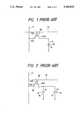
- FIG. 1is a diagram showing an equivalent circuit of each pixel in a conventional liquid crystal display device having the active matrix structure.
- Reference numeral 11indicates a data line, 13 a gate line, 20 a thin film transistor (TFT), and 24S the source of the thin film transistor 20, the source 24S being connected to the data line 11.
- Reference numeral 24Ddenotes the drain of the thin film transistor 20 and 13G the gate of the thin film transistor 20, the gate 13G being connected to the gate bus 13.
- Reference numeral 14represents a transparent pixel electrode connected to the drain 24D, 15 a transparent common electrode formed on one of two opposed base plates (not shown) with a liquid crystal layer sandwiched therebetween, and 16 a pixel capacitance formed by the transparent pixel electrode 14 and the transparent common electrode 15.
- the pixel capacitance 16is charged by a drive voltage which is applied to the data line 11 corresponding to an image signal, and the potential of the pixel capacitance 16 relative to the common electrode 15 is controlled. In other words, a voltage corresponding to the image signal is written into the pixel capacitance 16. Then, when the thin film transistor 20 is turned OFF, the voltage written in the pixel capacitance 16 is retained and stored. This mechanism is the same as that of a semiconductor memory DRAM.
- the DRAMuses each capacitor as a storage element for writing therein and reading thereout information
- the liquid crystal display deviceuses the voltage of the pixel capacitance 16 to effect a molecular orientation of the liquid crystal forming a dielectric of the pixel capacitance 16 and the retention of the molecular orientation.
- the quantity of light passing through the pixel capacitance 16is controlled, by which the function of a display element is performed.
- the voltage written in the pixel capacitance 16decreases owing to various leakage currents.
- amorphous silicon used for the thin film transistor 20is so high in photoconductivity as to be employed for a photosensor, and when the thin film transistor 20 is exposed to light, a leakage current between the source 24S and the drain 24D materially increases.
- the conductivity of the liquid crystal itselfis greatly temperature-dependent, a temperature rise significantly impairs its insulation, causing a self-discharge of the liquid crystal capacitance 16.
- the leakage current of the thin film transistor 20also increases with the temperature rise.
- the voltage of the pixel capacitance 16decreases owing to such various leakage currents and the retention of the orientation of the liquid crystal becomes unstable accordingly--this is perceived as a decrease in the contrast of a display or a flicker, incurring degradation of the display quality.
- reference numeral 18denotes a light blocking layer for blocking light incident to the thin film transistor 20.
- the light blocking layer 18is formed of an opaque metal.
- the thin film 20is of an inversely staggered structure, the light blocking layer 18 is provided on the liquid crystal side, whereas when the thin film transistor 20 is of a staggered structure, the light blocking layer 18 is provided on the base plate with an insulating film sandwiched therebetween.
- Reference numeral 17indicates a storage capacitance electrode disposed opposite the transparent pixel electrode 14. The storage capacitance electrode 17 is connected to a storage capacitance line dedicated thereto or to the gate line 13 of the preceding stage.
- Reference numeral 19denotes a signal storage capacitance formed by the transparent pixel electrode 14 and the storage capacitance electrode 17.
- a dielectric of the signal storage capacitance 19is formed by a silicon oxide film, silicon nitride film, or similar stable insulating film which has an excellent insulating property.
- the liquid crystal display device of such an active matrix structureincludes the light blocking layer 18 as mentioned above, and hence affords substantial reduction of the leakage current which results from the incidence of light to the thin film transistor 20. Furthermore, since the signal storage capacitance 19 is provided in parallel to the pixel capacitance 16, the amount of charge stored in the total capacitance can be greatly increased, and consequently, even if the self-discharge of the pixel capacitance 16 and the leakage current of the thin film transistor 20 increase owing to a temperature rise or the like, the voltage variation of the pixel capacitance 16 can be held within a given limit. Thus, the stability of orientation of the liquid crystal increases and a decrease in the contrast of a display can be avoided.
- Such a liquid crystal display deviceincludes the light blocking layer 18 and the signal storage capacitance 19, however, the number of its manufacturing steps increases and the manufacturing cost rises accordingly. For instance, the formation of the light blocking layer 18 calls for the steps of depositing metal, patterning it and depositing an insulating film.
- the storage capacitance electrode 17is connected to the gate line 13 of the preceding stage, there is no need of providing a dedicated storage capacitance line, and consequently, the number of manufacturing steps does not increase, but the load on the gate line 13 increases so much that it is difficult to apply the liquid crystal display device to a large display, and at the same time, the necessity of sequential scanning imposes severe limitations on the drive system used.
- the storage capacitance electrode 17when the storage capacitance electrode 17 is connected to the storage capacitance line, the load on the gate line 13 is so small that the liquid crystal display device can be applied to a large display, but the formation of the storage capacitance line increases the number of manufacturing steps and hence raises the manufacturing costs.
- At least light blocking layers for blocking light incident to thin film transistors, and storage capacitance electrodes opposite transparent pixel electrodes and storage capacitance lines to which the storage capacitance electrodes are connectedare formed by the same layer of the same material on a glass base plate, each of the thin film transistors is formed so that it overlaps the light blocking layer through an insulating film, and the transparent pixel electrode is formed in a manner to overlap the storage capacitance electrode through the insulating film.
- the provision of the light blocking layerpermits substantial reduction of the leakage current resulting from the incidence of light to the thin film transistor, and the provision of the storage capacitance electrode allows a substantial increase in the amount of charge to be stored in the pixel capacitance.
- the light blocking layers, the storage capacitance electrodes and the storage capacitance linesare formed by the same layer of the same material, an increase in the number of manufacturing steps is held minimum.
- FIG. 1is a schematic diagram for explaining a conventional active matrix structure
- FIG. 2is a schematic diagram for explaining another conventional active matrix structure provided with a signal storage capacitance
- FIG. 3is a plan view illustrating the vicinity of one pixel in the active matrix structure according to the present invention.
- FIG. 4is a sectional view taken on the line IV--IV in FIG. 3;
- FIG. 5is a plan view showing a portion of the peripheral terminal area of the active matrix structure according to the present invention.
- FIG. 6is a sectional view taken on the line VI--VI in FIG. 5;
- FIG. 7is a graph showing the etching rate of a molybdenum-chromium alloy film
- FIG. 8is a sectional view showing one pixel and its vicinity in the active matrix structure employing the molybdenum-chromium alloy film for wiring;
- FIG. 9is a graph showing the relationship between the concentration of nitrogen in a sputtering gas and the etching rate of a molybdenum film formed by sputtering;
- FIG. 10is a sectional view showing an example of etching of a molybdenum-aluminum multilayer interconnection deposited by sputtering without using nitrogen;
- FIG. 11is a sectional view showing an example of etching of a molybdenum-aluminum multilayer interconnection deposited by sputtering using nitrogen;
- FIG. 12is a sectional view showing an example of etching of a molybdenum multilayer interconnection deposited by sputtering using nitrogen and without using it;
- FIG. 13is a sectional view showing an example of etching of a molybdenum film deposited by sputtering while successively changing the concentration of nitrogen.
- FIG. 3is a plan view showing one pixel and its vicinity in the active matrix structure according to the present invention
- FIG. 4is a sectional view taken on the line IV--IV in FIG. 3, wherein each thin film transistor is of a staggered form.
- reference numeral 10designates a glass base plate
- 29designates a storage capacitance line to which a storage capacitance electrode 17 is connected.
- light blocking layers 18, storage capacitance electrodes 17 and storage capacitance lines 29 extending in the row directionare formed by the same layer of the same material, for example, an aluminum layer 100 nm thick.
- Reference numeral 12denotes an insulating layer deposited almost all over the base plate 10, covering the light blocking layers 18, the storage capacitance electrodes 17 and the storage capacitance lines 19.
- the insulating layer 12is formed by, for instance, a silicon nitride film.
- the storage capacitance electrodes 17are disposed opposite the corresponding transparent pixel electrodes 14 across the insulating layer 12, forming signal storage capacitances 19.
- the pixel electrode 14is formed of indium-tin-oxide (ITO).
- ITOindium-tin-oxide
- the light blocking layer 18underlies the thin film transistor 20 and a parasitic capacitance between a source electrode 22 and a drain electrode 23, which poses a problem in terms of driving, is also determined by the material and thickness of the insulating layer 12; therefore, the thickness of the insulating layer 12 must be selected to be a suitable value.
- the insulating layer 12is, for example, 500 nm in thickness.
- each data line 11comprises an ITO layer 11a formed on the insulating layer 12 and a molybdenum-base alloy layer 11b covering the ITO layer 11a, and the ITO layer 11a is formed simultaneously with the formation of the pixel electrode 14.
- the ITO layer 11a of the data line 11 and the pixel electrode 14are extended toward each other and their opposed marginal portions form the source and drain electrodes 22 and 23, respectively.
- An amorphous silicon semiconductor layer 24bridges across a gap between the source and drain electrodes 22 and 23. Almost all over the base plate 10 there is coated a gate insulating film 25 common to all the thin film transistors 20, covering the data lines 11, the pixel electrodes 14 and the semiconductor layers 24.
- the gate insulating film 25is formed by a 300 nm thick silicon nitride film, on which there is formed a gate line 13 extending over the semiconductor layers 24 of each row, and a portion of the gate line 13 overlapping each semiconductor layer 24 constitutes a gate electrode 13G.
- a semiconductor layer 24ais also formed over the data line 11 at each intersection of the data line 11 and the gate line 13 at the same time as the semiconductor layer 24 of the thin film transistors (hereinafter referred to as the TFT) 20 are formed.
- the semiconductor layer 24aincreases, in cooperation with the gate insulating film 25, the reliability of insulation between the data line 11 and the gate line 13 at their intersection.
- FIG. 5is a plan view showing matrix terminals at the peripheral portion of the base plate 10.
- FIG. 6is a sectional view taken on the line VI--VI in FIG. 5.
- a line connection land 29Lis formed integrally with one end portion of each of storage capacitance lines 29 extending from a display area 100.
- the gate insulating film 25 and the insulating layer 12are selectively etched to form a window 28 through which each line connection land 29L is exposed. Near or over the array of such line connection lands 29L there is formed on the insulating layer 12 a capacitance connection land 32L of the same material as that of the data line 11.
- the capacitance connection land 32Lis connected via a wire 32W to an external connection terminal 32X formed integrally with the wire 32W at one marginal portion of the base plate 10.
- the data lines 11 extended out from the display area 100are connected to external connection terminals 11X which are arranged on the insulating layer 12 along one marginal side of the base plate 10 in side-by-side relation to one another and to the terminal 32X, the terminals 11X being formed of the same material as that of the data lines 11.
- the gate insulating film 25has windows 11A and 32A through which the external connection terminals 11X and 32X are exposed. Outside of the display area 100 there are formed an array of line connection lands 33L corresponding to the gate lines 13, the line connection lands 33L being made of the same material as that of the data lines 11.
- the line connection lands 33Lare extended to form gate line external connection terminals 33X arranged along the marginal edge of another side of the base plate 10.
- the gate insulating film 25has windows 33H and 33A to expose therethrough the line connection lands 33L and the external connection terminals 33X, respectively.
- the gate lines 13 extended outwardly of the display area 100have their end portions connected to the connection lands 33L through the windows 33H corresponding thereto.
- the line connection lands 29Lcan be formed of the same material as that of the light blocking layers 18, the storage capacitance electrodes 17 and the storage capacitance lines 29 and at the same time as the formation of them.
- the external connection terminals 11X extended from the data lines 11, the line connection lands 33L connected to the gate lines 13, the external connection terminals 33X extended from the line connection lands 33L, the capacitance connection lands 32L and the external connection terminals 32X extended therefromcan be all formed on the insulating layer 12, using the same material as that of the data lines 11 and at the same time as the lines 11 are formed.
- connection line 31can also be formed of the same material as that of the gate lines 13 and at the same time.
- the active matrix structure described aboveit is possible to effectively prevent deterioration of the display image quality, partly because the provision of the light blocking layer 18 affords substantial reduction of the leakage current which is caused by the incidence of light to the thin film transistor 20, and partly because the provision of the storage capacitance electrode 17 allows a substantial increase in the amount of charge to be stored in the pixel electrode 14. Furthermore, since the light blocking layers 18, the storage capacitance electrodes 17 and the storage capacitance lines 29 are formed by the same layer of the same material, the number of manufacturing steps is minimized, and consequently, the manufacturing costs are low.
- the windows 27, 28 and 32A for the connection of the individual storage capacitance lines 29 and the windows 11A, 33A and 33H for the connection of the data lines 11 and the gate lines 13can be simultaneously formed by a parallel plate electrode dry etching process using a gas of the carbon fluoride series; this also minimizes the number of manufacturing steps involved and hence keeps down the manufacturing costs.
- the light blocking layers 18, the storage capacitance electrodes 17 and the storage capacitance lines 29are described to be formed of aluminum, they may also be formed of chromium (Cr), tantalum (Ta), titanium (Ti), copper (Cu) or silver (Ag), or a composite metal consisting principally of each of them, or their alloy, and when aluminum (Al), copper (Cu) and silver (Ag) are used, the resistance of the storage capacitance lines 29 can be reduced.
- the insulating layer 12is described to be formed by the silicon nitride film but it may also be formed by a silicon oxide film, tantalum oxide film, or a combination thereof, and the thickness of the insulating layer 12 may also be in the range of between 100 and 1000 nm, although it is described to be 500 nm thick in the above embodiment.
- the gate insulating film 25is described to be formed by a silicon nitride film, it may also be formed by a silicon oxide film, tantalum oxide film, or a combination thereof.
- the capacitance connection land 32L, the wire 32W and the external connection terminal 32Xare formed by the same layers as those of the source electrodes 22, the drain electrodes 23 and the data lines 11 in the above embodiment, but they may also be formed by the same layers as those of the gate lines 13, the gate electrodes 13G and the connection line 31 or by the same layers as those of the light blocking layers 18, the storage capacitance electrodes 17, the storage capacitance lines 29 and the line connection lands 29L.
- the above-mentioned active matrix structureis entirely covered with a passivation film deposited except at the marginal portions of the base plate 10 where the windows 11A, 32A and 33A for external connection are provided.
- the active matrix structure according to the present inventionpermits a substantial reduction of the leakage currents which result from the irradiation of the thin film transistors by light and allows a substantial increase in the amount of charge which can be stored in the pixel capacitances; hence, the display image quality will not be deteriorated.
- the manufacturing costs of the active matrix structureare low, because the number of manufacturing steps involved is kept to a minimum.
- simultaneous formation of the windows for the connection of the storage capacitance lines and the windows for the connection of the matrix lines of the thin film transistorsminimizes the number of manufacturing steps involved, and hence keeps down the manufacturing costs.
- any of the storage capacitance electrodes 17, the storage capacitance lines 29, the light blocking layers 18, the data lines 11 and the gate lines 13may be formed of aluminum (Al), tungsten (W), molybdenum (Mo), chromium (Cr), tantalum (Ta), titanium (Ti), etc.
- Aluminum (Al)is particularly suitable for the lines 11, 13 and 29 because it is low in electric resistance, and it is also suitable for the light blocking layers 18 because of its high reflectivity of light.
- an aluminum thin filmis defective in that hillocks are readily formed on its film surface at a relatively low temperature, say, hundreds of degrees.
- molybdenumthough appreciably higher in its electric resistance than aluminum (Al), is a refractory metal and hence is excellent in heat resistance, and further, because of its higher workability by chemical wet etching than other refractory metals, it is employed widely as a material for an integrated circuit such as an LSI, as an electrode material for a thin film device using thin film transistors, and as a wiring material.
- the molybdenum filmhas a defect that in the course of photolithography or chemical wet etching the developer or etchant is liable to enter the film in the direction of its thickness, i.e. along the columnar texture, damaging the underlying materials.
- an active matrix LCDliquid crystal display
- the corrosion of the ITOcan be avoided, but in the case of the sputtering-deposited molybdenum film of the columnar texture, the infiltration thereinto of the developer or aluminum etchant is likely to occur, and consequently, the ITO may sometimes be impaired and its corrosion cannot completely be prevented.
- the edge of its patternbecomes vertical, and as a result of this, an overlying interconnection layer may be broken or the overlying insulating film may be shorted because of its insufficient voltage endurance.
- the etchantenters into the columnar texture boundaries of the molybdenum film and corrodes the underlying material, and the etching rate of the underlying molybdenum film is so high that an overhang is liable to be formed.
- a molybdenum-chromium alloy filmwas formed as a metal thin film for use as each of the light blocking layers 18, the storage capacitance electrodes 17, the storage capacitance lines 29, the data lines 11 and the gate lines 13.
- a molybdenum (Mo) target containing 0 to 10 wt% of chromiumwas fabricated by sintering, and then a film was deposited thereon by use of a DC magnetron sputtering device.
- the electric power for sputteringwas 800 W and the pressure of argon of the atmosphere of sputtering was held at 3.0 mTorr.
- the film deposition ratewas not dependent on the chromium (Cr) content but was equal to that in the case of pure molybdenum.
- the molybdenum-chromium alloy film to substrateswere studied.
- the molybdenum-chromium (hereinafter expressed also by MoCr x , where x indicates the composition ratio of chromium) alloywas deposited on each of glass, stainless steel and silicon (Si) substrates of 3 ⁇ m thick, without heating the substrates.
- the substrateswere each cut by a cutter into squares and then subjected to a tape peeling test.
- the pure molybdenum filmwas easily peeled from each of the substrates, but molybdenum films containing chromium were apparently difficult to peel off.
- the chromium contained in the molybdenum-base alloy filmmarkedly improves its resistance to gases of fluorine series such as CF 4 .
- FIG. 7shows an example, where the abscissa represents the chromium content (in wt%) in the molybdenum-base alloy and the ordinate represents the etching rate (in nm/min). As shown, an increase in the chromium content decreases the etching rate down to about 1/4 that of the pure molybdenum film. Taking into account the selection ratio of chromium to other materials, patterning by the etching gases of this series is virtually impossible.
- the attack of the molybdenum wiring pattern containing chromium, by the etching gascan be suppressed very small.
- the etching ratealso somewhat decreases, as compared with that of the pure molybdenum film, owing to the chromium contained, but the decrease in the etching rate in this case is not as marked as in the case of using the CF 4 -series gas. Accordingly, the chlorine-series gas can be used for patterning, and in the present inventors' experiments it did not present any problem in the fine wiring process.
- the electric resistance of the molybdenum-chromium alloy filmincreases monotonously with an increase in the chromium content.
- the pure molybdenum film produced under the above-mentioned conditionshas a resistivity of about 10 to 15 ⁇ cm, but when the chromium content is 5%, the resistivity is 30 ⁇ cm and when the chromium content is 10%, the resistivity is around 40 ⁇ cm, which is substantially equal to the resistivities of chromium and tantalum wires. This eliminates the merits of molybdenum as a wiring material and therefore the chromium content should preferably be held under 10%.
- the molybdenum-base alloy thin film containing 0.5 to 10 wt% of chromiumis a desirable material for the lines 11, 13 and 29 or the light blocking layers 18 and the storage capacitance electrodes 17 in the liquid crystal display element.
- the resistance of each line 11, 13, 29can be further reduced when it is formed by laminating such a molybdenum-base alloy layer and an ITO layer.
- the electric resistance of matrix line wiringsbegins to exert a serious influence on the uniformity of display characteristics of their display screens.
- the matrix line wiring materialhas a resistivity in the range of 10 to 20 ⁇ cm
- the size of a panel on which a display of satisfactory image quality can be providedis about 10 inches at the largest.
- the above-mentioned MoCr x thin film added with 0.5 to 10 wt% of chromiumexhibits excellent adhesion to a silicon nitride film and an ITO film. It has also been found that the MoCr x thin film is easy to etch with the aluminum etchant and that the laminated film patterned by etching has gently sloping side walls toward the substrate. Thus, the aforementioned disadvantages of using aluminum in the active matrix structure can be sufficiently be compensated for by laminating the MoCr x thin film and the aluminum film.
- FIG. 8illustrates in section one thin film transistor and its vicinity in an active matrix structure in which the gate line 13 and the data line 11 are formed by laminating MoCr x and aluminum layers and an inverse staggered TFT structure is employed.
- This active matrix structurewas fabricated in the manner described below.
- each gate line 13has a structure in which a MoCr x layer 13B overlies an aluminum layer 13a as depicted in FIG. 8.
- the gate electrodes 13G, the storage capacitance electrodes 17 and the storage capacitance lines 29also have the same structure as that of the gate lines 13.
- Each gate electrode 13functions also as a light blocking layer.
- the side wall of the patternhas an inclination of approximately 50 degrees and a defect in a stepped portion of a film coated on the side wall could be avoided.
- a silicon nitride film as the gate insulating film 25an amorphous silicon film as a semiconductor active layer 24 and a silicon nitride film as an active layer protecting film 21 were deposited, in succession, by a plasma CVD process to form an active area.
- the aforementioned hillockwas grown by heating of the substrate during the plasma CVD process, so that the surface of the layer was roughened, and characteristics of the thin film transistor formed on such a layer were deteriorated and the number of shorts increased remarkably.
- the above-mentioned laminated wiring layerwas free from the generation of hillock and its surface remained smooth.
- each data line 11has a structure in which the aluminum layer 11a overlies the MoCr x layer 11b.
- the ITO layer forming the pixel electrode 14 and the drain 24Dmade completely ohmic contact with each other.
- Sheet resistances of the data line 11 and the gate line 13, calculated from their measured resistance values,were favorable, i.e. 0.4 and 0.15 ⁇ , respectively; in particular, the sheet resistance of the gate line 13 was one or more orders of magnitude smaller than in the cases of conventional chromium and tantalum wiring layers.
- the inventionis also applicable to an active matrix structure employing the staggered type thin film transistor.
- the resistance of the underlayer data linecan be decreased; namely, the data line, which is usually required to be high-speed, can be made low in resistance, and consequently, the effect by the introduction of the aluminum laminated wiring structure is especially remarkable.
- argonis usually employed as the sputtering gas, but it has been found that the etching rate of the molybdenum film decreases in the case where it is deposited using, as the sputtering gas, a mixture of argon and nitrogen.
- FIG. 9shows the relationship between the nitrogen mixing ratio and the etching rate. When nitrogen is mixed 20% by volume, the etching rate of the molybdenum film by an ordinary aluminum etchant, which consists principally of phosphoric acid, is 1/4 of the etching rate in the case of argon 100%.
- the inclination of the side wall of the pattern edgewhich was close to 90 degrees after etching, decreases with an increase in the nitrogen mixing ratio, and with the 20% nitrogen mixing ratio the inclination angle did not become 45 degrees obtainable with isotropic etching but became approximately 50 degrees.
- the above-described phenomenon by mixing nitrogen into argonis considered to be caused by the fact that the presence of nitrogen in the sputtering gas promotes changing of the structure of the molybdenum film from the columnar to a homogeneous structure with an increase in the nitrogen mixing ratio, densifying the film structure.
- ITOwas deposited 500 ⁇ thick on a glass substrate (Corning #7059) by a DC magnetron sputtering method while heating the substrate at 200° C. to obtain a sample substrate.
- a molybdenum filmwas deposited 100 nm thick on the sample substrate, using as the sputtering gas argon mixed with 10% of nitrogen (N 2 ).
- the sputtering device usedwas of the sputter-up system in which a carrier with a sample set thereon 50 mm above the target was moved.
- the molybdenum targetwas of a size measuring 5 inches (12.7 cm) by 15 inches (38.1 cm) and its purity was 99.9 wt% or higher.
- the samplewas heated at 100° C.
- the sputtering gas usedwas a mixture of argon 27SCCM (Ncm 3 /min) and N 2 (3SCCM), and its pressure was 3.0 mTorr.
- the electric power for sputteringwas 1 kW at 2.0 A and at about 500 V. Under such conditions the molybdenum film was deposited 100 nm thick when the travel speed of the substrate was 120 mm/min. Following this, aluminum was deposited 200 nm thick on the molybdenum film by use of the same sputtering device.
- the conditions for sputtering the aluminum filmwere as follows:
- the sputtering gaswas argon 30SCCM held under a pressure of 30 mTorr, the electric power for the sputtering was 3 kW at 6.0 A, and the substrate was moved at a rate of 120 mm/min and heated at 100° C.
- ITO50 nm
- molybdenum10 nm
- This structureis intended for low-resistance matrix line wiring of the liquid crystal display and is used for preventing the ITO layer from corrosion by the galvanic reaction in the case where the aluminum layer is laminated directly on the ITO layer.
- a positive photoresist(Shiplay, Microposite 1400-31) was coated 1.5 ⁇ m thick by use of a spinner, exposed through a mask to print thereon a predetermined wiring mask and then developed using a two-fold diluted developer (Shiplay, MF-312).
- This developeris an amine-series developer of appreciable alkalinity, and in the case of a molybdenum film deposited using the conventional sputtering gas composed only of argon, the underlying ITO layer is impaired by the developer.
- the substrate assemblywas subjected to hard baking at 120° C. for 10 minutes and then the aluminum film and the molybdenum film were successively etched with an etchant consisting of phosphoric acid, acetic acid and nitric acid in the ratio of 20 to 3 to 1.
- an etchantconsisting of phosphoric acid, acetic acid and nitric acid in the ratio of 20 to 3 to 1.
- the ITO layerwas corroded frequently also in this etching process, for the same reason as mentioned above, but in this example, the ITO layer was not impaired at all.
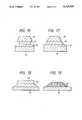
- the molybdenum filmis deposited using the conventional sputtering gas consisting only of argon, it is side etched as indicated by 43 in FIG. 10, so that the overlying aluminum film 45 overhangs the molybdenum film 43 at the marginal edge of the etched pattern as shown.
- the molybdenum film 44 deposited using the sputtering gas mixed with 10% of nitrogen (N 2 ) according to this examplethe molybdenum film 44 and the aluminum film 45 are continuously inclined to form smoothly tapered marginal edges of the etched pattern as shown in FIG. 11.
- the nitrogen-mixed sputtering gasdecreases the etching rate of the molybdenum film down to the vicinity of the etching rate of the aluminum film 45 and makes the molybdenum film structure homogeneous and densified.
- the inclination of the pattern edgewas around 90 degrees partly because the nitrogen mixing ratio was 10%, but the inclination of the underlying molybdenum film 44 could be further reduced by increasing the nitrogen mixing ratio.
- Molybdenumwas deposited 100 nm thick on a glass substrate (Corning, #7059), using a sputtering gas having 20% of nitrogen mixed with argon.
- the sputtering device usedwas the same as that used in Example 1.
- the molybdenum targetwas also of a size measuring 5 inches by 15 inches and its purity was also 99.9% or higher as in Example 1.
- the samplewas heated at 100° C. and its temperature was maintained during sputtering.
- the sputtering gaswas composed of argon 24 SCCM and nitrogen (N 2 ) 6 SCCM and its pressure was 3.0 mTorr.
- the electric power for the sputteringwas 1 kW at 2.0 A and 500 V.
- the carrier travel speedwas 120 mm/min.
- the sputtering gaswas switched to a sputtering gas consisting 100% of argon and the molybdenum film was deposited another 100 nm thick under the following sputtering conditions:
- the sputtering gaswas composed of argon 30 SCCM, its pressure was 3.0 mTorr, and the electric power was 800 W at 2.0 A and 400 V.
- a predetermined wiring patternwas printed on this two-layer molybdenum film by use of a positive photoresist and then subjected to etching by an etchant consisting of phosphoric acid, acetic acid and nitric acid in the ratio of 20 to 3 to 1.
- the sectional configuration of the wiring patternwas observed by a scanning electron microscope.
- the underlying molybdenum film 44had a tapered marginal portion and the overlying molybdenum film 43 had a vertical side wall.
- the electric resistance of this multilayer film, converted from its sheet resistance,was 2.8 ⁇ 10 -5 ⁇ cm.
- the electric resistanceis 7.0 ⁇ 10 5 ⁇ cm; accordingly, the resistance of the two-layer film structure is more than one-half of the resistance of the single-layer film structure.
- the nitrogen mixing ratio of the sputtering gasis increased early in the film deposition by sputtering and then the mixing ratio is suitably decreased in accordance with the growth of the film, by which the marginal edge can be gently sloped as depicted in FIG. 13 and an increase in the wiring resistance can be suppressed.
- a molybdenum filmis deposited by sputtering by use of a sputtering gas mixed with nitrogen, and the use of such a sputtering gas makes the film structure of the molybdenum film homogeneous and dense; so that its etching rate decreases, making it possible to provide a wiring pattern structure having tapered marginal edges with high reproducibility.
Landscapes
- Physics & Mathematics (AREA)
- Nonlinear Science (AREA)
- Engineering & Computer Science (AREA)
- Mathematical Physics (AREA)
- Chemical & Material Sciences (AREA)
- Crystallography & Structural Chemistry (AREA)
- General Physics & Mathematics (AREA)
- Optics & Photonics (AREA)
- Microelectronics & Electronic Packaging (AREA)
- Power Engineering (AREA)
- Liquid Crystal (AREA)
- Thin Film Transistor (AREA)
Abstract
Description
Claims (20)
Applications Claiming Priority (8)
| Application Number | Priority Date | Filing Date | Title |
|---|---|---|---|
| JP12408090AJP2813234B2 (en) | 1990-05-16 | 1990-05-16 | Wiring structure |
| JP2-124081 | 1990-05-16 | ||
| JP2-124080 | 1990-05-16 | ||
| JP2-124076 | 1990-05-16 | ||
| JP2-124075 | 1990-05-16 | ||
| JP12407690AJP2803759B2 (en) | 1990-05-16 | 1990-05-16 | Active matrix structure and manufacturing method thereof |
| JP2124075AJP3046829B2 (en) | 1990-05-16 | 1990-05-16 | Method for forming molybdenum film |
| JP02124081AJP3112275B2 (en) | 1990-05-16 | 1990-05-16 | Wiring materials for thin film components |
Publications (1)
| Publication Number | Publication Date |
|---|---|
| US5162933Atrue US5162933A (en) | 1992-11-10 |
Family
ID=27471004
Family Applications (1)
| Application Number | Title | Priority Date | Filing Date |
|---|---|---|---|
| US07/697,991Expired - LifetimeUS5162933A (en) | 1990-05-16 | 1991-05-10 | Active matrix structure for liquid crystal display elements wherein each of the gate/data lines includes at least a molybdenum-base alloy layer containing 0.5 to 10 wt. % of chromium |
Country Status (4)
| Country | Link |
|---|---|
| US (1) | US5162933A (en) |
| EP (1) | EP0457328B1 (en) |
| KR (1) | KR950002943B1 (en) |
| DE (1) | DE69116218T2 (en) |
Cited By (126)
| Publication number | Priority date | Publication date | Assignee | Title |
|---|---|---|---|---|
| US5296653A (en)* | 1991-12-09 | 1994-03-22 | Kabushiki Kaisha Toshiba | Device having a multi-layered conductor structure |
| US5349205A (en)* | 1991-12-02 | 1994-09-20 | Matsushita Electric Industrial Co., Ltd. | Thin-film transistor array with anodic oxide for use in a liquid crystal display |
| US5426523A (en)* | 1992-05-13 | 1995-06-20 | Sharp Kabushiki Kaisha | Liquid crystal display having a light blocking film on stepped portions |
| US5432625A (en)* | 1992-03-30 | 1995-07-11 | France Telecom Etablissement Autonome De Droit Public | Display screen having opaque conductive optical mask and TFT of semiconductive, insulating, and conductive layers on first transparent conductive film |
| US5453856A (en)* | 1992-12-10 | 1995-09-26 | Goldstar Co., Ltd. | Liquid crystal display with gate lines connected with a doped semiconductor layer where they cross data lines |
| US5499123A (en)* | 1992-10-27 | 1996-03-12 | Nec Corporation | Active matrix liquid crystal display cell with light blocking capacitor electrode above insulating layer |
| US5500787A (en)* | 1989-10-09 | 1996-03-19 | Sharp Kabushiki Kaisha | Electrodes on a mounting substrate and a liquid crystal display apparatus including same |
| US5521465A (en)* | 1992-12-14 | 1996-05-28 | Westinghouse Norden Systems Inc. | Sunlight viewable thin film electroluminscent display having darkened metal electrodes |
| US5528082A (en)* | 1994-04-28 | 1996-06-18 | Xerox Corporation | Thin-film structure with tapered feature |
| US5539551A (en)* | 1992-12-28 | 1996-07-23 | Casio Computer Co., Ltd. | LCD TFT drain and source electrodes having ohmic barrier, primary conductor, and liquid impermeable layers and method of making |
| US5561440A (en)* | 1990-08-08 | 1996-10-01 | Hitachi, Ltd. | Liquid crystal display device and driving method therefor |
| US5633738A (en)* | 1994-05-27 | 1997-05-27 | Hitachi, Ltd. | TFT substrate having scanning lines of metal films of columnar crystal grains |
| US5691782A (en)* | 1994-07-08 | 1997-11-25 | Sanyo Electric Co., Ltd. | Liquid-crystal display with inter-line short-circuit preventive function and process for producing same |
| US5693983A (en)* | 1994-04-28 | 1997-12-02 | Xerox Corporation | Thin-film structure with conductive molybdenum-chromium line |
| US5731856A (en)* | 1995-12-30 | 1998-03-24 | Samsung Electronics Co., Ltd. | Methods for forming liquid crystal displays including thin film transistors and gate pads having a particular structure |
| US5739877A (en)* | 1994-11-18 | 1998-04-14 | Hitahci, Ltd. | Active matrix liquid crystal display in which the gate and/or drain lines are made of a Cr-Mo alloy |
| US5751381A (en)* | 1993-12-21 | 1998-05-12 | Hitachi, Ltd. | Active matrix LCD device with image signal lines having a multilayered structure |
| US5777701A (en)* | 1995-05-08 | 1998-07-07 | Semiconductor Energy Laboratory Co., Ltd. | Display device |
| US5782665A (en)* | 1995-12-29 | 1998-07-21 | Xerox Corporation | Fabricating array with storage capacitor between cell electrode and dark matrix |
| US5818552A (en)* | 1995-07-31 | 1998-10-06 | Sony Corporation | Transmissive display device having two reflection metallic layers of differing reflectances |
| US5825449A (en)* | 1995-08-19 | 1998-10-20 | Lg Electronics, Inc. | Liquid crystal display device and method of manufacturing the same |
| US5835168A (en)* | 1992-04-10 | 1998-11-10 | Matsushita Electric Industrial, Co., Ltd. | Active matrix liquid crystal having capacitance electrodes connected to pixel electrodes |
| US5912506A (en)* | 1996-10-15 | 1999-06-15 | International Business Machines Corporation | Multi-layer metal sandwich with taper and reduced etch bias and method for forming same |
| US5936292A (en)* | 1997-06-17 | 1999-08-10 | Nec Corporation | Structure of thin film transistor and gate terminal having a capacitive structure composed of the TFT elements |
| US5982460A (en)* | 1996-06-25 | 1999-11-09 | Semiconductor Energy Laboratory Co., Ltd. | Electro-optical display |
| US6005648A (en)* | 1996-06-25 | 1999-12-21 | Semiconductor Energy Laboratory Co., Ltd. | Display device |
| US6081308A (en)* | 1996-11-21 | 2000-06-27 | Samsung Electronics Co., Ltd. | Method for manufacturing liquid crystal display |
| US6111619A (en)* | 1999-05-27 | 2000-08-29 | Sharp Laboratories Of America, Inc. | Method of forming polycrystalline silicon TFTs with TiN/Cu/TiN interconnections for a liquid crystal display pixel array |
| US6115088A (en)* | 1996-09-04 | 2000-09-05 | Semiconductor Energy Laboratory Co., Ltd. | Display device |
| US6172733B1 (en)* | 1998-02-20 | 2001-01-09 | Lg.Philips Lcd Co., Ltd. | Liquid crystal display including conductive layer passing through multiple layers and method of manufacturing same |
| US6208390B1 (en)* | 1994-11-24 | 2001-03-27 | Kabushiki Kaisha Toshiba | Electrode substrate resistant to wire breakage for an active matrix display device |
| US6252247B1 (en)* | 1998-03-31 | 2001-06-26 | Mitsubishi Denki Kabushiki Kaisha | Thin film transistor, a method for producing the thin film transistor, and a liquid crystal display using a TFT array substrate |
| US20020007062A1 (en)* | 1997-03-24 | 2002-01-17 | Societe De Conseils De Recherches Et D' Applications Scientifiques (S.C.R.A.S.) | New derivatives of 2-(iminomethyl) amino-phenyl, their preparation, their use as medicaments and the pharmaceutical compositions containing them |
| US6346175B1 (en) | 1997-11-20 | 2002-02-12 | International Business Machines Corporation | Modification of in-plate refractory metal texture by use of refractory metal/nitride layer |
| US6356318B1 (en)* | 1999-06-28 | 2002-03-12 | Alps Electric Co., Ltd. | Active-matrix liquid crystal display having storage capacitors of area smaller than that of pixel electrodes |
| US6373546B1 (en)* | 1997-03-03 | 2002-04-16 | Lg Philips Lcd Co., Ltd. | Structure of a liquid crystal display and the method of manufacturing the same |
| US20020047947A1 (en)* | 1997-11-20 | 2002-04-25 | Myung-Keo Hur | Wire for liquid crystal displays, liquid crystal displays having the same, and manufacturing methods thereof |
| US6392721B1 (en)* | 1998-10-02 | 2002-05-21 | Hitachi, Ltd. | Liquid crystal display device having wiring line including first and second layers with second layer having a thickness not greater than 1/2 of a thickness of first layer |
| US6404473B1 (en)* | 1997-06-12 | 2002-06-11 | Hitachi, Ltd. | Display device having a wiring multi-layered structure with tapered first layer and a manufacturing process for the tapered structure |
| US20020093600A1 (en)* | 2001-01-18 | 2002-07-18 | Lg. Philips Lcd Co., Ltd. | Array substrate for a liquid crystal display device and method of manufacturing the same |
| US6433842B1 (en)* | 1999-03-26 | 2002-08-13 | Hitachi, Ltd. | Liquid crystal display device and method of manufacturing the same |
| US6449026B1 (en)* | 1999-06-25 | 2002-09-10 | Hyundai Display Technology Inc. | Fringe field switching liquid crystal display and method for manufacturing the same |
| US6522370B2 (en)* | 2000-11-10 | 2003-02-18 | Hitachi, Ltd. | Liquid crystal display units |
| US6537843B2 (en)* | 1996-12-06 | 2003-03-25 | Lg.Philips Lcd Co., Ltd | Thin film transistor and method of manufacturing the same |
| US6548829B2 (en) | 1997-03-04 | 2003-04-15 | Lg Lcd Inc. | Thin-film transistor |
| US6621537B1 (en)* | 1998-10-07 | 2003-09-16 | Advanced Display Inc. | Active matrix liquid crystal display and manufacturing method of the same |
| US6628361B2 (en)* | 2000-02-25 | 2003-09-30 | Hitachi, Ltd. | Liquid crystal display device and wiring structure therefor |
| US6653216B1 (en)* | 1998-06-08 | 2003-11-25 | Casio Computer Co., Ltd. | Transparent electrode forming apparatus and method of fabricating active matrix substrate |
| US6661026B2 (en) | 1995-11-21 | 2003-12-09 | Samsung Electronics Co., Ltd. | Thin film transistor substrate |
| US6690068B2 (en) | 2000-06-12 | 2004-02-10 | Semiconductor Energy Laboratory Co., Ltd. | Thin film transistors and semiconductor device |
| US20040036835A1 (en)* | 2002-08-20 | 2004-02-26 | Lg.Philips Lcd Co., Ltd. | Method for forming metal line of liquid crystal display device |
| US6703265B2 (en) | 2000-08-02 | 2004-03-09 | Semiconductor Energy Laboratory Co., Ltd. | Semiconductor device and method of manufacturing the same |
| US6713783B1 (en)* | 1991-03-15 | 2004-03-30 | Semiconductor Energy Laboratory Co., Ltd. | Compensating electro-optical device including thin film transistors |
| WO2004027503A1 (en)* | 2002-09-18 | 2004-04-01 | Samsung Electronics Co., Ltd. | Liquid crystal display |
| US20040065882A1 (en)* | 1999-01-21 | 2004-04-08 | Semiconductor Energy Laboratory Co., Ltd. | Semiconductor device and process for production thereof |
| US6720577B2 (en) | 2000-09-06 | 2004-04-13 | Semiconductor Energy Laboratory Co., Ltd. | Semiconductor device and method of manufacturing the same |
| US6724454B2 (en)* | 2000-10-20 | 2004-04-20 | Lg.Philips Lcd Co., Ltd | Ips lcd device having a light shielding layer under at least one common or data electrodes so that light transmittance areas of the common and data electrodes are the same and a method of manufacturing the same |
| US6741315B1 (en)* | 1999-08-27 | 2004-05-25 | Seiko Epson Corporation | Liquid crystal device and electronic apparatus |
| US20040119898A1 (en)* | 1999-10-29 | 2004-06-24 | Song Jang-Kun | Vertical alignment mode liquid crystal display |
| US20040164297A1 (en)* | 2003-02-19 | 2004-08-26 | Toshiki Kaneko | Display device |
| US20040169991A1 (en)* | 1999-03-11 | 2004-09-02 | Sharp Kabushiki Kaisha | Active matrix substrate, method of manufacturing the same, and image sensor incorporating the same |
| US6787807B2 (en) | 2000-06-19 | 2004-09-07 | Semiconductor Energy Laboratory Co., Ltd. | Semiconductor device |
| US6806933B2 (en)* | 1999-12-31 | 2004-10-19 | Lg. Philips Lcd Co., Ltd. | Array substrate with multi-layer electrode line |
| US20040212772A1 (en)* | 2000-05-25 | 2004-10-28 | Manabu Hanakawa | Liquid crystal device, manufacturing method therefor, and electronic apparatus |
| US20040218112A1 (en)* | 1997-05-22 | 2004-11-04 | Semiconductor Energy Laboratory Co., Ltd. | Electro-optical device |
| US20040223090A1 (en)* | 2000-09-14 | 2004-11-11 | Tomoaki Takahashi | Liquid crystal display device, manufacturing method thereof, and fabrication apparatus therefor |
| US6828587B2 (en)* | 2000-06-19 | 2004-12-07 | Semiconductor Energy Laboratory Co., Ltd. | Semiconductor device |
| US20040263708A1 (en)* | 2003-06-30 | 2004-12-30 | Won-Ho Cho | Array substrate for LCD device having metal-diffusion film and manufacturing method thereof |
| US20050181533A1 (en)* | 2004-02-02 | 2005-08-18 | Seiko Epson Corporation | Method for manufacturing an electro-optical device board, optical device, electro-optical device and electronic equipment |
| US20050250266A1 (en)* | 1993-01-18 | 2005-11-10 | Semiconductor Energy Laboratory Co., Ltd. | Semiconductor device having a gate oxide film with some NTFTS with LDD regions and no PTPTS with LDD regions |
| KR100516248B1 (en)* | 1996-11-01 | 2005-11-29 | 가부시끼가이샤 히다치 세이사꾸쇼 | Active Matrix Liquid Crystal Display and Liquid Crystal Display |
| US20050263768A1 (en)* | 2004-05-27 | 2005-12-01 | Lg. Philips Lcd Co., Ltd. | Liquid crystal display device and fabricating method thereof |
| US20050263769A1 (en)* | 2004-05-27 | 2005-12-01 | Byung Chul Ahn | Liquid crystal display device and fabricating method thereof |
| US20050270452A1 (en)* | 2004-06-05 | 2005-12-08 | Ahn Byung C | Liquid crystal display device and method of fabricating same |
| US20050270451A1 (en)* | 2004-06-05 | 2005-12-08 | Ahn Byung C | Liquid crystal display device and fabricating method thereof |
| US20050270434A1 (en)* | 2004-06-05 | 2005-12-08 | Jung Tae Y | Liquid crystal display device and fabricating method thereof |
| US20050270450A1 (en)* | 2004-06-05 | 2005-12-08 | Ahn Byung C | Liquid crystal display device and fabricating method thereof |
| US20050270453A1 (en)* | 2004-06-05 | 2005-12-08 | Lg. Philips Lcd Co., Ltd. | Liquid crystal display device and fabricating method thereof |
| US20050270454A1 (en)* | 2004-06-05 | 2005-12-08 | Ahn Byung C | Liquid crystal display device and fabricating method thereof |
| US20050269638A1 (en)* | 2004-06-05 | 2005-12-08 | Jung Tae Y | Liquid crystal display device and fabricating method thereof |
| US20060001791A1 (en)* | 2004-06-30 | 2006-01-05 | Hwang Seong S | Pad structure of liquid crystal display device and fabrication method thereof |
| US20060017054A1 (en)* | 2004-06-24 | 2006-01-26 | Ahn Byung C | Liquid crystal display device and fabricating method thereof |
| US20060081870A1 (en)* | 2002-12-25 | 2006-04-20 | Nec Lcd Technologies, Ltd. | Method of forming a lamination film pattern and improved lamination film pattern |
| US20060119771A1 (en)* | 2004-12-04 | 2006-06-08 | Lim Joo S | Liquid crystal display device and fabricating method thereof |
| US20060138417A1 (en)* | 2004-12-24 | 2006-06-29 | Ahn Byung C | Liquid crystal display device and fabricating method thereof |
| US20060138428A1 (en)* | 2004-12-24 | 2006-06-29 | Ahn Byung C | Liquid crystal display device and fabricating method thereof, and thin film patterning method applied thereto |
| US20060139504A1 (en)* | 2004-12-24 | 2006-06-29 | Ahn Byung C | Liquid crystal display device and fabricating method thereof |
| US20060139502A1 (en)* | 2004-12-24 | 2006-06-29 | Ahn Byung C | Liquid crystal display device and fabricating method thereof |
| US20060139548A1 (en)* | 2004-12-24 | 2006-06-29 | Ahn Byung C | Liquid crystal display device and fabricating method thereof |
| US20060139556A1 (en)* | 2004-12-23 | 2006-06-29 | Ahn Byung C | Liquid crystal display panel and method of fabricating the same |
| US20060139554A1 (en)* | 2004-12-23 | 2006-06-29 | Park Jong W | Liquid crystal display panel and fabricating method thereof |
| US20060146245A1 (en)* | 2004-12-31 | 2006-07-06 | Ahn Byung C | Liquid crystal display device and fabricating method thereof |
| US20060146213A1 (en)* | 2004-12-31 | 2006-07-06 | Ahn Byung C | Liquid crystal display device and fabricating method thereof |
| US20060146212A1 (en)* | 2004-12-31 | 2006-07-06 | Ahn Byung C | Liquid crystal display device and fabricating method thereof |
| US20060145161A1 (en)* | 2004-12-31 | 2006-07-06 | Ji No Lee | Liquid crystal display device and method for fabricating the same |
| US20060146217A1 (en)* | 2004-12-31 | 2006-07-06 | Ahn Byung C | Liquid crystal display device and fabricating method thereof |
| US20060146216A1 (en)* | 2004-12-31 | 2006-07-06 | Ahn Byung C | Liquid crystal display device and fabricating method thereof |
| US20060284193A1 (en)* | 2005-06-17 | 2006-12-21 | Lg Electronics Inc. | Organic electroluminescent device |
| US20060290867A1 (en)* | 2005-06-27 | 2006-12-28 | Ahn Byung C | Liquid crystal display and fabricating method thereof |
| US20070001979A1 (en)* | 2005-06-30 | 2007-01-04 | Lg Philips Lcd Co., Ltd. | Method of forming fine pattern, liquid crystal display device having a fine pattern and fabricating method thereof |
| US20070000431A1 (en)* | 2005-06-30 | 2007-01-04 | Lg.Philips Lcd Co., Ltd. | Method of repairing a short defect and a method of fabricating a liquid crystal display device |
| US20070002249A1 (en)* | 2005-06-30 | 2007-01-04 | Yoo Soon S | Liquid crystal display device and fabricating method thereof |
| US20070103614A1 (en)* | 2005-11-07 | 2007-05-10 | Samsung Electronics Co., Ltd. | Thin film transistor array panel for liquid crystal display |
| US20070146606A1 (en)* | 2005-12-28 | 2007-06-28 | Lg.Philips Lcd Co., Ltd. | Liquid crystal display device and method of driving the same |
| US20070165173A1 (en)* | 2005-12-28 | 2007-07-19 | Nagayama Kazuyoshi | Liquid crystal display device |
| US20070165175A1 (en)* | 2005-12-28 | 2007-07-19 | Nagayama Kazuyoshi | Liquid crystal display device |
| US20070165174A1 (en)* | 2005-12-28 | 2007-07-19 | Nagayama Kazuyoshi | Liquid crystal display device and method of fabricating the same |
| US20070176872A1 (en)* | 2005-12-28 | 2007-08-02 | Lg.Philips Lcd Co.,Ltd. | Liquid crystal display device |
| US20070188691A1 (en)* | 2005-12-28 | 2007-08-16 | Lg.Philips Lcd Co., Ltd. | Liquid crystal display device and method of fabricating thereof |
| US20070200989A1 (en)* | 2005-12-28 | 2007-08-30 | Lg.Philips Lcd Co., Ltd. | Liquid crystal display device and the method thereof |
| US20080067324A1 (en)* | 2006-09-14 | 2008-03-20 | Heiler Gregory N | High fill-factor sensor with reduced coupling |
| US20080121415A1 (en)* | 2006-11-27 | 2008-05-29 | Lg.Philips Lcd Co., Ltd. | Method for manufacturing flexible display device and flexible display device |
| US20090256153A1 (en)* | 1995-05-31 | 2009-10-15 | Sharp Kabushiki Kaisha | Thin film transistor matrix device and method for fabricating the same |
| US7643122B2 (en) | 2004-06-30 | 2010-01-05 | Lg Display Co., Ltd. | LCD device having data line disposed within, and data link disposed outside liquid crystal region and crossing a sealant region and with gate insulating film in contact with upper surface of the data link |
| US20100047946A1 (en)* | 2003-06-30 | 2010-02-25 | Sang-Gab Kim | Thin film array panel and manufacturing method thereof |
| US20100163877A1 (en)* | 2006-09-15 | 2010-07-01 | Kabushiki Kaisha Kobe Seiko Sho (Kobe Steel, Ltd.) | Display device |
| US20100214792A1 (en)* | 2007-03-13 | 2010-08-26 | Chen Chia-Li | Luminous pedal for a bicycle |
| US20110216269A1 (en)* | 2010-03-08 | 2011-09-08 | Casio Computer Co., Ltd. | Liquid crystal display device |
| US8064024B2 (en) | 2004-12-04 | 2011-11-22 | Lg Display Co., Ltd. | Transflective thin film transistor substrate of liquid crystal display device having a contact electrode connecting a data link to a data line |
| US8179505B2 (en) | 2004-12-23 | 2012-05-15 | Lg Display Co., Ltd. | Transflective type liquid crystal display device having a color layer in the transmissive region and a non-color layer in the reflective region and fabricating method thereof |
| US8492768B2 (en)* | 1998-12-18 | 2013-07-23 | Semiconductor Energy Laboratory Co., Ltd. | Semiconductor device and method of fabricating the same |
| US9494815B2 (en)* | 2012-12-24 | 2016-11-15 | Shanghai Tianma Micro-electronics Co., Ltd. | TN liquid crystal display device and touch control method thereof |
| US20170160610A1 (en)* | 2015-09-01 | 2017-06-08 | Shenzhen China Star Optoelectronics Technology Co. Ltd. | Boa liquid crystal panel |
| US20210074739A1 (en)* | 2019-09-10 | 2021-03-11 | Seiko Epson Corporation | Electro-optical device, method for manufacturing electro-optical device, and electronic apparatus |
| CN113421916A (en)* | 2021-05-27 | 2021-09-21 | 重庆惠科金渝光电科技有限公司 | Preparation method of metal conductive film, thin film transistor and display device |
| US11460744B2 (en)* | 2020-04-10 | 2022-10-04 | Samsung Display Co., Ltd. | Display device and method of manufacturing the same |
Families Citing this family (8)
| Publication number | Priority date | Publication date | Assignee | Title |
|---|---|---|---|---|
| TW226044B (en)* | 1992-04-15 | 1994-07-01 | Toshiba Co Ltd | |
| JPH07199150A (en)* | 1993-12-28 | 1995-08-04 | Canon Inc | Liquid crystal display |
| JPH07318978A (en)* | 1994-05-20 | 1995-12-08 | Sony Corp | Thin film transistor array for display element |
| FR2732781B1 (en)* | 1995-04-07 | 1997-06-20 | Thomson Lcd | METHOD FOR MANUFACTURING TFT ACTIVE MATRIX FOR PROJECTION SYSTEM SCREEN |
| JPH08306926A (en)* | 1995-05-07 | 1996-11-22 | Semiconductor Energy Lab Co Ltd | Liquid crystal electrooptical system |
| TWI228625B (en) | 1995-11-17 | 2005-03-01 | Semiconductor Energy Lab | Display device |
| KR100500682B1 (en)* | 1996-11-28 | 2005-10-14 | 비오이 하이디스 테크놀로지 주식회사 | LCD and its manufacturing method |
| KR100697368B1 (en)* | 2000-11-20 | 2007-03-20 | 비오이 하이디스 테크놀로지 주식회사 | Manufacturing Method of Thin Film Transistor Liquid Crystal Display |
Citations (7)
| Publication number | Priority date | Publication date | Assignee | Title |
|---|---|---|---|---|
| US4770498A (en)* | 1982-07-12 | 1988-09-13 | Hosiden Electronics Co., Ltd. | Dot-matrix liquid crystal display |
| US4810060A (en)* | 1987-01-22 | 1989-03-07 | Hosiden Electronics Co. Ltd. | Active color liquid crystal display element compensating for differing voltage-transmission curves of the primary colors |
| US4821092A (en)* | 1986-11-27 | 1989-04-11 | Nec Corporation | Thin film transistor array for liquid crystal display panel |
| US4853296A (en)* | 1986-10-22 | 1989-08-01 | Toppan Printing Co., Ltd. | Electrode plate for color display device |
| US4869576A (en)* | 1985-10-04 | 1989-09-26 | Hosiden Electronics Co., Ltd. | Liquid-crystal display device employing a common electrode consisting of interconnected common electrode sections |
| US4906072A (en)* | 1986-10-09 | 1990-03-06 | Canon Kabushiki Kaisha | Display apparatus and driving method for providing an uniform potential to the electrodes |
| US4948231A (en)* | 1984-04-09 | 1990-08-14 | Hosiden Electronics Co. Ltd. | Liquid crystal display device and method of manufacturing the same |
Family Cites Families (2)
| Publication number | Priority date | Publication date | Assignee | Title |
|---|---|---|---|---|
| US4859036A (en)* | 1987-05-15 | 1989-08-22 | Canon Kabushiki Kaisha | Device plate having conductive films selected to prevent pin-holes |
| JPH01217325A (en)* | 1988-02-25 | 1989-08-30 | Sharp Corp | Liquid crystal display device |
- 1991
- 1991-05-10USUS07/697,991patent/US5162933A/ennot_activeExpired - Lifetime
- 1991-05-16EPEP91107967Apatent/EP0457328B1/ennot_activeExpired - Lifetime
- 1991-05-16DEDE69116218Tpatent/DE69116218T2/ennot_activeExpired - Fee Related
- 1991-05-16KRKR1019910007935Apatent/KR950002943B1/ennot_activeExpired - Fee Related
Patent Citations (7)
| Publication number | Priority date | Publication date | Assignee | Title |
|---|---|---|---|---|
| US4770498A (en)* | 1982-07-12 | 1988-09-13 | Hosiden Electronics Co., Ltd. | Dot-matrix liquid crystal display |
| US4948231A (en)* | 1984-04-09 | 1990-08-14 | Hosiden Electronics Co. Ltd. | Liquid crystal display device and method of manufacturing the same |
| US4869576A (en)* | 1985-10-04 | 1989-09-26 | Hosiden Electronics Co., Ltd. | Liquid-crystal display device employing a common electrode consisting of interconnected common electrode sections |
| US4906072A (en)* | 1986-10-09 | 1990-03-06 | Canon Kabushiki Kaisha | Display apparatus and driving method for providing an uniform potential to the electrodes |
| US4853296A (en)* | 1986-10-22 | 1989-08-01 | Toppan Printing Co., Ltd. | Electrode plate for color display device |
| US4821092A (en)* | 1986-11-27 | 1989-04-11 | Nec Corporation | Thin film transistor array for liquid crystal display panel |
| US4810060A (en)* | 1987-01-22 | 1989-03-07 | Hosiden Electronics Co. Ltd. | Active color liquid crystal display element compensating for differing voltage-transmission curves of the primary colors |
Cited By (297)
| Publication number | Priority date | Publication date | Assignee | Title |
|---|---|---|---|---|
| US7408233B2 (en)* | 1919-01-18 | 2008-08-05 | Semiconductor Energy Laboratory Co., Ltd. | Semiconductor device having N-channel thin film transistor with LDD regions and P-channel thin film transistor with LDD region |
| US5500787A (en)* | 1989-10-09 | 1996-03-19 | Sharp Kabushiki Kaisha | Electrodes on a mounting substrate and a liquid crystal display apparatus including same |
| US6331845B1 (en) | 1990-08-08 | 2001-12-18 | Hitachi, Ltd | Liquid crystal display device and driving method therefor |
| US6064358A (en)* | 1990-08-08 | 2000-05-16 | Hitachi, Ltd. | Liquid crystal display device and driving method therefor |
| US5561440A (en)* | 1990-08-08 | 1996-10-01 | Hitachi, Ltd. | Liquid crystal display device and driving method therefor |
| US6713783B1 (en)* | 1991-03-15 | 2004-03-30 | Semiconductor Energy Laboratory Co., Ltd. | Compensating electro-optical device including thin film transistors |
| US5349205A (en)* | 1991-12-02 | 1994-09-20 | Matsushita Electric Industrial Co., Ltd. | Thin-film transistor array with anodic oxide for use in a liquid crystal display |
| US5296653A (en)* | 1991-12-09 | 1994-03-22 | Kabushiki Kaisha Toshiba | Device having a multi-layered conductor structure |
| US5432625A (en)* | 1992-03-30 | 1995-07-11 | France Telecom Etablissement Autonome De Droit Public | Display screen having opaque conductive optical mask and TFT of semiconductive, insulating, and conductive layers on first transparent conductive film |
| US5835168A (en)* | 1992-04-10 | 1998-11-10 | Matsushita Electric Industrial, Co., Ltd. | Active matrix liquid crystal having capacitance electrodes connected to pixel electrodes |
| US5426523A (en)* | 1992-05-13 | 1995-06-20 | Sharp Kabushiki Kaisha | Liquid crystal display having a light blocking film on stepped portions |
| US5499123A (en)* | 1992-10-27 | 1996-03-12 | Nec Corporation | Active matrix liquid crystal display cell with light blocking capacitor electrode above insulating layer |
| US5453856A (en)* | 1992-12-10 | 1995-09-26 | Goldstar Co., Ltd. | Liquid crystal display with gate lines connected with a doped semiconductor layer where they cross data lines |
| US5521465A (en)* | 1992-12-14 | 1996-05-28 | Westinghouse Norden Systems Inc. | Sunlight viewable thin film electroluminscent display having darkened metal electrodes |
| US5539551A (en)* | 1992-12-28 | 1996-07-23 | Casio Computer Co., Ltd. | LCD TFT drain and source electrodes having ohmic barrier, primary conductor, and liquid impermeable layers and method of making |
| US20050250266A1 (en)* | 1993-01-18 | 2005-11-10 | Semiconductor Energy Laboratory Co., Ltd. | Semiconductor device having a gate oxide film with some NTFTS with LDD regions and no PTPTS with LDD regions |
| USRE39798E1 (en)* | 1993-12-21 | 2007-08-28 | Hitachi, Ltd. | Active matrix LCD device with image signal lines having a multilayered structure |
| US5751381A (en)* | 1993-12-21 | 1998-05-12 | Hitachi, Ltd. | Active matrix LCD device with image signal lines having a multilayered structure |
| US5693983A (en)* | 1994-04-28 | 1997-12-02 | Xerox Corporation | Thin-film structure with conductive molybdenum-chromium line |
| US5528082A (en)* | 1994-04-28 | 1996-06-18 | Xerox Corporation | Thin-film structure with tapered feature |
| US5756372A (en)* | 1994-05-27 | 1998-05-26 | Hitachi, Ltd. | Method of making liquid crystal display |
| US5633738A (en)* | 1994-05-27 | 1997-05-27 | Hitachi, Ltd. | TFT substrate having scanning lines of metal films of columnar crystal grains |
| US5691782A (en)* | 1994-07-08 | 1997-11-25 | Sanyo Electric Co., Ltd. | Liquid-crystal display with inter-line short-circuit preventive function and process for producing same |
| US5739877A (en)* | 1994-11-18 | 1998-04-14 | Hitahci, Ltd. | Active matrix liquid crystal display in which the gate and/or drain lines are made of a Cr-Mo alloy |
| US6208390B1 (en)* | 1994-11-24 | 2001-03-27 | Kabushiki Kaisha Toshiba | Electrode substrate resistant to wire breakage for an active matrix display device |
| US5777701A (en)* | 1995-05-08 | 1998-07-07 | Semiconductor Energy Laboratory Co., Ltd. | Display device |
| US20070153169A1 (en)* | 1995-05-08 | 2007-07-05 | Semiconductor Energy Laboratory Co., Ltd. | Display device |
| US7683978B2 (en) | 1995-05-08 | 2010-03-23 | Semiconductor Energy Laboratory Co., Ltd. | Display device |
| US7190420B2 (en) | 1995-05-08 | 2007-03-13 | Semiconductor Energy Laboratory Co., Ltd. | Display device |
| US7110059B2 (en) | 1995-05-08 | 2006-09-19 | Semiconductor Energy Laboratory Co., Ltd. | Display device |
| US20050099557A1 (en)* | 1995-05-08 | 2005-05-12 | Semiconductor Laboratory Co., Ltd., A Japan Corporation | Display device |
| US20100117087A1 (en)* | 1995-05-31 | 2010-05-13 | Sharp Kabushiki Kaisha | Thin film transistor matrix device and method for fabricating the same |
| US7947982B2 (en) | 1995-05-31 | 2011-05-24 | Sharp Kabushiki Kaisha | Thin film transistor matrix device including a plurality of thin film transistors arranged on the substrate |
| US8258513B2 (en) | 1995-05-31 | 2012-09-04 | Sharp Kabushiki Kaisha | Thin film transistor matrix device including first and second connection lines |
| US20090256153A1 (en)* | 1995-05-31 | 2009-10-15 | Sharp Kabushiki Kaisha | Thin film transistor matrix device and method for fabricating the same |
| US8592816B2 (en) | 1995-05-31 | 2013-11-26 | Sharp Kabushiki Kaisha | Thin film transistor matrix device including first and second connection lines |
| US20100214202A1 (en)* | 1995-05-31 | 2010-08-26 | Sharp Kabushiki Kaisha | Thin film transistor matrix device and method for fabricating the same |
| US7947983B2 (en) | 1995-05-31 | 2011-05-24 | Sharp Kabushiki Kaisha | Thin film transistor matrix device including first and second conducting connections formed outside an image display region |
| US6067131A (en)* | 1995-07-31 | 2000-05-23 | Sony Corporation | Transmissive display device having two reflection metallic layers of differing reflectances |
| US5818552A (en)* | 1995-07-31 | 1998-10-06 | Sony Corporation | Transmissive display device having two reflection metallic layers of differing reflectances |
| US5825449A (en)* | 1995-08-19 | 1998-10-20 | Lg Electronics, Inc. | Liquid crystal display device and method of manufacturing the same |
| US6661026B2 (en) | 1995-11-21 | 2003-12-09 | Samsung Electronics Co., Ltd. | Thin film transistor substrate |
| USRE41363E1 (en)* | 1995-11-21 | 2010-06-01 | Samsung Electronics Co., Ltd. | Thin film transistor substrate |
| US5782665A (en)* | 1995-12-29 | 1998-07-21 | Xerox Corporation | Fabricating array with storage capacitor between cell electrode and dark matrix |
| US5731856A (en)* | 1995-12-30 | 1998-03-24 | Samsung Electronics Co., Ltd. | Methods for forming liquid crystal displays including thin film transistors and gate pads having a particular structure |
| US5982460A (en)* | 1996-06-25 | 1999-11-09 | Semiconductor Energy Laboratory Co., Ltd. | Electro-optical display |
| US20050146667A1 (en)* | 1996-06-25 | 2005-07-07 | Semiconductor Energy Laboratory Co., Ltd., A Japan Corporation | Electro-optical device |
| US6097454A (en)* | 1996-06-25 | 2000-08-01 | Semiconductor Energy Laboratory Co., Ltd. | Display device |
| US6246453B1 (en) | 1996-06-25 | 2001-06-12 | Semiconductor Energy Laboratory Co., Ltd. | Electro-optical device |
| US7206053B2 (en) | 1996-06-25 | 2007-04-17 | Semiconductor Energy Laboratory Co., Ltd. | Electro-optical device |
| US6005648A (en)* | 1996-06-25 | 1999-12-21 | Semiconductor Energy Laboratory Co., Ltd. | Display device |
| US20070182873A1 (en)* | 1996-06-25 | 2007-08-09 | Semiconductor Energy Laboratory Co., Ltd. | Electro-optical device |
| US6914260B2 (en) | 1996-06-25 | 2005-07-05 | Semiconductor Energy Laboratory Co., Ltd. | Electro-optical device |
| US7542103B2 (en) | 1996-06-25 | 2009-06-02 | Semiconductor Energy Laboratory | Electro-optical device |
| US6421101B1 (en) | 1996-09-04 | 2002-07-16 | Semiconductor Energy Laboratory Co., Ltd. | Display device including a transparent electrode pattern covering and extending along gate & source lines |
| US7023502B2 (en) | 1996-09-04 | 2006-04-04 | Semiconductor Energy Laboratory Co., Ltd. | Semiconductor device having light-shielded thin film transistor |
| US8536577B2 (en) | 1996-09-04 | 2013-09-17 | Semiconductor Energy Laboratory Co., Ltd. | Display device |
| US20060192201A1 (en)* | 1996-09-04 | 2006-08-31 | Semiconductor Energy Laboratory Co., Ltd. | Display device |
| US6115088A (en)* | 1996-09-04 | 2000-09-05 | Semiconductor Energy Laboratory Co., Ltd. | Display device |
| US7646022B2 (en) | 1996-09-04 | 2010-01-12 | Semiconductor Energy Laboratory Co., Ltd. | Display device |
| US7863618B2 (en) | 1996-09-04 | 2011-01-04 | Semiconductor Energy Laboratory Co., Ltd. | Display device |
| US20050151891A1 (en)* | 1996-09-04 | 2005-07-14 | Semiconductor Energy Laboratory Co., Ltd., A Japan Corporation | Display Device |
| US20100044714A1 (en)* | 1996-09-04 | 2010-02-25 | Semiconductor Energy Laboratory Co., Ltd. | Display device |
| US20020171780A1 (en)* | 1996-09-04 | 2002-11-21 | Hongyong Zhang | Display device |
| US7046313B2 (en) | 1996-09-04 | 2006-05-16 | Semiconductor Energy Laboratory Co., Ltd. | Semiconductor device including a source line formed on interlayer insulating film having flattened surface |
| US20110163315A1 (en)* | 1996-09-04 | 2011-07-07 | Semiconductor Energy Laboratory Co., Ltd. | Display device |
| US8586985B2 (en) | 1996-09-04 | 2013-11-19 | Semiconductor Energy Laboratory Co., Ltd. | Display device |
| US5912506A (en)* | 1996-10-15 | 1999-06-15 | International Business Machines Corporation | Multi-layer metal sandwich with taper and reduced etch bias and method for forming same |
| KR100516248B1 (en)* | 1996-11-01 | 2005-11-29 | 가부시끼가이샤 히다치 세이사꾸쇼 | Active Matrix Liquid Crystal Display and Liquid Crystal Display |
| US6081308A (en)* | 1996-11-21 | 2000-06-27 | Samsung Electronics Co., Ltd. | Method for manufacturing liquid crystal display |
| US6537843B2 (en)* | 1996-12-06 | 2003-03-25 | Lg.Philips Lcd Co., Ltd | Thin film transistor and method of manufacturing the same |
| US6373546B1 (en)* | 1997-03-03 | 2002-04-16 | Lg Philips Lcd Co., Ltd. | Structure of a liquid crystal display and the method of manufacturing the same |
| US6614500B2 (en) | 1997-03-03 | 2003-09-02 | Lg Philips Lcd Co., Ltd. | Liquid crystal display having a dummy source pad and method for manufacturing the same |
| US6815321B2 (en) | 1997-03-04 | 2004-11-09 | Lg. Philips Lcd Co., Ltd. | Thin-film transistor and method of making same |
| US7176489B2 (en) | 1997-03-04 | 2007-02-13 | Lg. Philips Lcd. Co., Ltd. | Thin-film transistor and method of making same |
| USRE45841E1 (en) | 1997-03-04 | 2016-01-12 | Lg Display Co., Ltd. | Thin-film transistor and method of making same |
| US6548829B2 (en) | 1997-03-04 | 2003-04-15 | Lg Lcd Inc. | Thin-film transistor |
| US20030164520A1 (en)* | 1997-03-04 | 2003-09-04 | Lg Lcd Inc. | Thin-film transistor and method of making same |
| USRE45579E1 (en) | 1997-03-04 | 2015-06-23 | Lg Display Co., Ltd. | Thin-film transistor and method of making same |
| US20040229413A1 (en)* | 1997-03-04 | 2004-11-18 | Lg Lcd Inc. | Thin-film transistor and method of making same |
| US20020007062A1 (en)* | 1997-03-24 | 2002-01-17 | Societe De Conseils De Recherches Et D' Applications Scientifiques (S.C.R.A.S.) | New derivatives of 2-(iminomethyl) amino-phenyl, their preparation, their use as medicaments and the pharmaceutical compositions containing them |
| US8854593B2 (en) | 1997-05-22 | 2014-10-07 | Semiconductor Energy Laboratory Co., Ltd. | Electro-optical device |
| US8045125B2 (en) | 1997-05-22 | 2011-10-25 | Semiconductor Energy Laboratory Co., Ltd. | Liquid crystal display device having a gap retaining member made of resin formed directly over the driver circuit |
| US20040218112A1 (en)* | 1997-05-22 | 2004-11-04 | Semiconductor Energy Laboratory Co., Ltd. | Electro-optical device |
| US6404473B1 (en)* | 1997-06-12 | 2002-06-11 | Hitachi, Ltd. | Display device having a wiring multi-layered structure with tapered first layer and a manufacturing process for the tapered structure |
| US5936292A (en)* | 1997-06-17 | 1999-08-10 | Nec Corporation | Structure of thin film transistor and gate terminal having a capacitive structure composed of the TFT elements |
| US7173683B2 (en)* | 1997-11-20 | 2007-02-06 | Samsung Electronics Co., Ltd. | Wire for liquid crystal displays, liquid crystal displays having the same, and manufacturing methods thereof |
| US20020047947A1 (en)* | 1997-11-20 | 2002-04-25 | Myung-Keo Hur | Wire for liquid crystal displays, liquid crystal displays having the same, and manufacturing methods thereof |
| US6346175B1 (en) | 1997-11-20 | 2002-02-12 | International Business Machines Corporation | Modification of in-plate refractory metal texture by use of refractory metal/nitride layer |
| US6172733B1 (en)* | 1998-02-20 | 2001-01-09 | Lg.Philips Lcd Co., Ltd. | Liquid crystal display including conductive layer passing through multiple layers and method of manufacturing same |
| US6252247B1 (en)* | 1998-03-31 | 2001-06-26 | Mitsubishi Denki Kabushiki Kaisha | Thin film transistor, a method for producing the thin film transistor, and a liquid crystal display using a TFT array substrate |
| US6653216B1 (en)* | 1998-06-08 | 2003-11-25 | Casio Computer Co., Ltd. | Transparent electrode forming apparatus and method of fabricating active matrix substrate |
| US6392721B1 (en)* | 1998-10-02 | 2002-05-21 | Hitachi, Ltd. | Liquid crystal display device having wiring line including first and second layers with second layer having a thickness not greater than 1/2 of a thickness of first layer |
| US6621537B1 (en)* | 1998-10-07 | 2003-09-16 | Advanced Display Inc. | Active matrix liquid crystal display and manufacturing method of the same |
| US8492768B2 (en)* | 1998-12-18 | 2013-07-23 | Semiconductor Energy Laboratory Co., Ltd. | Semiconductor device and method of fabricating the same |
| US9368642B2 (en) | 1998-12-18 | 2016-06-14 | Semiconductor Energy Laboratory Co., Ltd. | Semiconductor device and method of fabricating the same |
| US20130299832A1 (en)* | 1998-12-18 | 2013-11-14 | Semiconductor Energy Laboratory Co., Ltd. | Semiconductor device and method of fabricating the same |
| US8816347B2 (en)* | 1998-12-18 | 2014-08-26 | Semiconductor Energy Laboratory Co., Ltd. | Semiconductor device and method of fabricating the same |
| US7727836B2 (en) | 1999-01-21 | 2010-06-01 | Semiconductor Energy Laboratory Co., Ltd. | Semiconductor device and process for production thereof |
| US6890784B2 (en)* | 1999-01-21 | 2005-05-10 | Semiconductor Energy Laboratory Co., Ltd. | Semiconductor device and process for production thereof |
| US20050253149A1 (en)* | 1999-01-21 | 2005-11-17 | Semiconductor Energy Laboratory Co., Ltd. | Semiconductor device and process for production thereof |
| US20040065882A1 (en)* | 1999-01-21 | 2004-04-08 | Semiconductor Energy Laboratory Co., Ltd. | Semiconductor device and process for production thereof |
| US20070194362A1 (en)* | 1999-01-21 | 2007-08-23 | Semiconductor Energy Laboratory Co., Ltd. | Semiconductor Device and Process for Production Thereof |
| US7208766B2 (en) | 1999-01-21 | 2007-04-24 | Semiconductor Energy Laboratory Co., Ltd. | Semiconductor device and process for production thereof |
| US20090057670A1 (en)* | 1999-01-21 | 2009-03-05 | Semiconductor Energy Laboratory Co., Ltd. | Semiconductor Device and Process for Production Thereof |
| US7414267B2 (en) | 1999-01-21 | 2008-08-19 | Semiconductor Energy Laboratory Co., Ltd. | Semiconductor device and process for production thereof |
| US20040169991A1 (en)* | 1999-03-11 | 2004-09-02 | Sharp Kabushiki Kaisha | Active matrix substrate, method of manufacturing the same, and image sensor incorporating the same |
| US7250991B2 (en)* | 1999-03-11 | 2007-07-31 | Sharp Kabushiki Kaisha | Active matrix substrate, method of manufacturing the same, and image sensor incorporating the same |
| US6433842B1 (en)* | 1999-03-26 | 2002-08-13 | Hitachi, Ltd. | Liquid crystal display device and method of manufacturing the same |
| US6111619A (en)* | 1999-05-27 | 2000-08-29 | Sharp Laboratories Of America, Inc. | Method of forming polycrystalline silicon TFTs with TiN/Cu/TiN interconnections for a liquid crystal display pixel array |
| US6449026B1 (en)* | 1999-06-25 | 2002-09-10 | Hyundai Display Technology Inc. | Fringe field switching liquid crystal display and method for manufacturing the same |
| US6356318B1 (en)* | 1999-06-28 | 2002-03-12 | Alps Electric Co., Ltd. | Active-matrix liquid crystal display having storage capacitors of area smaller than that of pixel electrodes |
| US6741315B1 (en)* | 1999-08-27 | 2004-05-25 | Seiko Epson Corporation | Liquid crystal device and electronic apparatus |
| US6972811B2 (en)* | 1999-10-29 | 2005-12-06 | Samsung Electronics Co., Ltd. | Pixel electrode structure for liquid crystal display |
| US20040119898A1 (en)* | 1999-10-29 | 2004-06-24 | Song Jang-Kun | Vertical alignment mode liquid crystal display |
| US6806933B2 (en)* | 1999-12-31 | 2004-10-19 | Lg. Philips Lcd Co., Ltd. | Array substrate with multi-layer electrode line |
| US6628361B2 (en)* | 2000-02-25 | 2003-09-30 | Hitachi, Ltd. | Liquid crystal display device and wiring structure therefor |
| US20040212772A1 (en)* | 2000-05-25 | 2004-10-28 | Manabu Hanakawa | Liquid crystal device, manufacturing method therefor, and electronic apparatus |
| US7092050B2 (en)* | 2000-05-25 | 2006-08-15 | Seiko Epson Corporation | Liquid crystal device, manufacturing method therefor, and electronic apparatus |
| US7307282B2 (en) | 2000-06-12 | 2007-12-11 | Semiconductor Energy Laboratory Co., Ltd. | Thin film transistors and semiconductor device |
| US20040108576A1 (en)* | 2000-06-12 | 2004-06-10 | Semiconductor Energy Laboratory, Co., Ltd., A Japan Corporation | Thin film transistors and semiconductor device |
| US6690068B2 (en) | 2000-06-12 | 2004-02-10 | Semiconductor Energy Laboratory Co., Ltd. | Thin film transistors and semiconductor device |
| US6787807B2 (en) | 2000-06-19 | 2004-09-07 | Semiconductor Energy Laboratory Co., Ltd. | Semiconductor device |
| US20040201022A1 (en)* | 2000-06-19 | 2004-10-14 | Semiconductor Energy Laboratory Co., Ltd. | Semiconductor device |
| US6956235B2 (en) | 2000-06-19 | 2005-10-18 | Semiconductor Energy Laboratory Co., Ltd. | Semiconductor device |
| US6828587B2 (en)* | 2000-06-19 | 2004-12-07 | Semiconductor Energy Laboratory Co., Ltd. | Semiconductor device |
| US7368335B2 (en) | 2000-08-02 | 2008-05-06 | Semiconductor Energy Laboratory Co., Ltd. | Semiconductor device and method of manufacturing the same |
| US20060246638A1 (en)* | 2000-08-02 | 2006-11-02 | Semiconductor Energy Laboratory Co., Ltd. | Semiconductor Device and Method of Manufacturing the Same |
| US6703265B2 (en) | 2000-08-02 | 2004-03-09 | Semiconductor Energy Laboratory Co., Ltd. | Semiconductor device and method of manufacturing the same |
| US7034337B2 (en) | 2000-08-02 | 2006-04-25 | Semiconductor Energy Laboratory Co., Ltd. | Semiconductor device and method of manufacturing the same |
| US20040169177A1 (en)* | 2000-08-02 | 2004-09-02 | Semiconductor Energy Laboratory Co., Ltd. A Japan Corporation | Semiconductor device and method of manufacturing the same |
| US20060071215A1 (en)* | 2000-09-06 | 2006-04-06 | Semiconductor Energy Laboratory Co., Ltd. | Semiconductor device and method of manufacturing the same |
| US6963084B2 (en) | 2000-09-06 | 2005-11-08 | Semiconductor Energy Laboratory Co., Ltd. | Semiconductor device having a storage capacitor |
| US20040144983A1 (en)* | 2000-09-06 | 2004-07-29 | Semiconductor Energy Laboratory Co., Ltd. | Semiconductor device and method of manufacturing the same |
| US6720577B2 (en) | 2000-09-06 | 2004-04-13 | Semiconductor Energy Laboratory Co., Ltd. | Semiconductor device and method of manufacturing the same |
| US7977680B2 (en) | 2000-09-06 | 2011-07-12 | Semiconductor Energy Laboratory Co., Ltd. | Semiconductor device having thin film transistors on a metal substrate |
| US20080272376A1 (en)* | 2000-09-06 | 2008-11-06 | Semiconductor Energy Laboratory Co., Ltd. | Semiconductor Device and Method of Manufacturing the Same |
| US7405132B2 (en) | 2000-09-06 | 2008-07-29 | Semiconductor Energy Laboratory Co., Ltd. | Method of making a thin film transistor device |
| US6903786B2 (en) | 2000-09-14 | 2005-06-07 | Hitachi, Ltd. | Liquid crystal display device, manufacturing method thereof, and fabrication apparatus therefor |
| US20040223090A1 (en)* | 2000-09-14 | 2004-11-11 | Tomoaki Takahashi | Liquid crystal display device, manufacturing method thereof, and fabrication apparatus therefor |
| US6724454B2 (en)* | 2000-10-20 | 2004-04-20 | Lg.Philips Lcd Co., Ltd | Ips lcd device having a light shielding layer under at least one common or data electrodes so that light transmittance areas of the common and data electrodes are the same and a method of manufacturing the same |
| US8446553B2 (en) | 2000-10-20 | 2013-05-21 | Lg Display Co., Ltd. | In-plane switching mode liquid crystal display device and method of manufacturing the same |
| US20040218131A1 (en)* | 2000-10-20 | 2004-11-04 | Kim Gi Hong | In-plane switchiing mode liquid crystal display device and method of manufacturing the same |
| US8212984B2 (en) | 2000-10-20 | 2012-07-03 | Lg Display Co., Ltd. | Method of manufacturing an IPS LCD device having a light shielding layer under at least one common or data electrodes so that light transmittance areas of the common and data electrodes are the same |
| US7522245B2 (en) | 2000-10-20 | 2009-04-21 | Lg Display Co., Ltd. | In-plane switching mode liquid crystal display device |
| US20070109479A1 (en)* | 2000-10-20 | 2007-05-17 | Kim Gi H | In-plane switching mode liquid crystal display device and method of manufacturing the same |
| US7173682B2 (en) | 2000-10-20 | 2007-02-06 | L.G.Philips Lcd Co., Ltd | In-plane switching mode liquid crystal display device and method of manufacturing the same |
| KR100481344B1 (en)* | 2000-11-10 | 2005-04-07 | 가부시키가이샤 히타치세이사쿠쇼 | Liquid crystal display units |
| US6522370B2 (en)* | 2000-11-10 | 2003-02-18 | Hitachi, Ltd. | Liquid crystal display units |
| US6707512B2 (en) | 2000-11-10 | 2004-03-16 | Hitachi, Ltd. | Liquid crystal display units with data line being formed of molybdenum alloy having chromium content |
| US7995182B2 (en)* | 2001-01-18 | 2011-08-09 | Lg Display Co., Ltd. | Array substrate for a liquid crystal display device and method of manufacturing the same |
| US20020093600A1 (en)* | 2001-01-18 | 2002-07-18 | Lg. Philips Lcd Co., Ltd. | Array substrate for a liquid crystal display device and method of manufacturing the same |
| US6930749B2 (en)* | 2002-08-20 | 2005-08-16 | Lg. Philips Lcd Co., Ltd. | Method for forming metal line of liquid crystal display device |
| US20040036835A1 (en)* | 2002-08-20 | 2004-02-26 | Lg.Philips Lcd Co., Ltd. | Method for forming metal line of liquid crystal display device |
| US7450190B2 (en)* | 2002-09-18 | 2008-11-11 | Samsung Electronics Co., Ltd. | Liquid-crystal display having a particular ratio of horizontal to vertical for each pixel |
| WO2004027503A1 (en)* | 2002-09-18 | 2004-04-01 | Samsung Electronics Co., Ltd. | Liquid crystal display |
| US20070040952A1 (en)* | 2002-09-18 | 2007-02-22 | Nam-Seok Roh | Liquid crystal display |
| US20060081870A1 (en)* | 2002-12-25 | 2006-04-20 | Nec Lcd Technologies, Ltd. | Method of forming a lamination film pattern and improved lamination film pattern |
| US7554207B2 (en)* | 2002-12-25 | 2009-06-30 | Nec Lcd Technologies, Ltd. | Method of forming a lamination film pattern and improved lamination film pattern |
| US20040164297A1 (en)* | 2003-02-19 | 2004-08-26 | Toshiki Kaneko | Display device |
| US7352417B2 (en)* | 2003-06-30 | 2008-04-01 | Lg.Philips Lcd Co., Ltd. | Array substrate for LCD device having metal-diffusion film and manufacturing method thereof |
| US7492420B2 (en) | 2003-06-30 | 2009-02-17 | Lg Display Co., Ltd. | Array substrate for LCD device having metal-diffusion film and manufacturing method thereof |
| US20100047946A1 (en)* | 2003-06-30 | 2010-02-25 | Sang-Gab Kim | Thin film array panel and manufacturing method thereof |
| US20080129943A1 (en)* | 2003-06-30 | 2008-06-05 | Won-Ho Cho | Array substrate for LCD device having metal-diffusion film and manufacturing method thereof |
| US20040263708A1 (en)* | 2003-06-30 | 2004-12-30 | Won-Ho Cho | Array substrate for LCD device having metal-diffusion film and manufacturing method thereof |
| US8093595B2 (en)* | 2003-06-30 | 2012-01-10 | Samsung Electronics Co., Ltd. | Thin film array panel and manufacturing method thereof |
| US20050181533A1 (en)* | 2004-02-02 | 2005-08-18 | Seiko Epson Corporation | Method for manufacturing an electro-optical device board, optical device, electro-optical device and electronic equipment |
| US20050263768A1 (en)* | 2004-05-27 | 2005-12-01 | Lg. Philips Lcd Co., Ltd. | Liquid crystal display device and fabricating method thereof |
| US8017462B2 (en) | 2004-05-27 | 2011-09-13 | Lg Display Co., Ltd. | Method of making a liquid crystal display device capable of increasing capacitance of storage capacitor |
| US7351623B2 (en) | 2004-05-27 | 2008-04-01 | Lg.Philips Lcd Co., Ltd. | Liquid crystal display device and fabricating method thereof |
| US20090085040A1 (en)* | 2004-05-27 | 2009-04-02 | Byung Chul Ahn | Liquid crystal display device and fabricating method thereof |
| US20050263769A1 (en)* | 2004-05-27 | 2005-12-01 | Byung Chul Ahn | Liquid crystal display device and fabricating method thereof |
| US7468527B2 (en) | 2004-05-27 | 2008-12-23 | Lg Display Co., Ltd. | Liquid crystal display device and fabricating method thereof |
| US8045072B2 (en) | 2004-05-27 | 2011-10-25 | Lg Display Co., Ltd. | Liquid crystal display device |
| US20050270450A1 (en)* | 2004-06-05 | 2005-12-08 | Ahn Byung C | Liquid crystal display device and fabricating method thereof |
| US7760309B2 (en) | 2004-06-05 | 2010-07-20 | Lg Display Co., Ltd. | Transflective liquid crystal display device and fabricating method thereof |
| US20050270454A1 (en)* | 2004-06-05 | 2005-12-08 | Ahn Byung C | Liquid crystal display device and fabricating method thereof |
| US20050270434A1 (en)* | 2004-06-05 | 2005-12-08 | Jung Tae Y | Liquid crystal display device and fabricating method thereof |
| US20050270453A1 (en)* | 2004-06-05 | 2005-12-08 | Lg. Philips Lcd Co., Ltd. | Liquid crystal display device and fabricating method thereof |
| US7439586B2 (en) | 2004-06-05 | 2008-10-21 | Lg Display Co., Ltd. | Liquid crystal display device and fabricating method thereof |
| US7312843B2 (en) | 2004-06-05 | 2007-12-25 | Lg.Philips Lcd Co., Ltd. | Liquid crystal display device and fabricating method thereof |
| US8072565B2 (en) | 2004-06-05 | 2011-12-06 | Lg Display Co., Ltd. | Transflective liquid crystal display device |
| US20090291517A1 (en)* | 2004-06-05 | 2009-11-26 | Byung Chul Ahn | Liquid crystal display device and fabricating method thereof |
| US20090290084A1 (en)* | 2004-06-05 | 2009-11-26 | Byung Chul Ahn | Liquid crystal display device and method of fabricating same |
| US20080094534A1 (en)* | 2004-06-05 | 2008-04-24 | Lg Philips Lcd Co., Ltd. | Liquid crystal display device and fabricating method thereof |
| US20050270451A1 (en)* | 2004-06-05 | 2005-12-08 | Ahn Byung C | Liquid crystal display device and fabricating method thereof |
| US8115893B2 (en) | 2004-06-05 | 2012-02-14 | Lg Display Co., Ltd. | Liquid crystal display device with reflection and transmission regions |
| US7518666B2 (en) | 2004-06-05 | 2009-04-14 | Lg Display Co., Ltd. | Liquid crystal display device and fabricating method thereof |
| US20050269638A1 (en)* | 2004-06-05 | 2005-12-08 | Jung Tae Y | Liquid crystal display device and fabricating method thereof |
| US7583336B2 (en) | 2004-06-05 | 2009-09-01 | Lg Display Co., Ltd. | Liquid crystal display device and fabricating method thereof |
| US7528909B2 (en) | 2004-06-05 | 2009-05-05 | Lg Display Co., Ltd. | Liquid crystal display device and fabricating method having reflective electrode connecting pixel electrode with drain and upper storage capacitor electrodes at edge of transmission hole |
| US7583337B2 (en) | 2004-06-05 | 2009-09-01 | Lg Display Co., Ltd. | Liquid crystal display device and method of fabricating same |
| US20050270452A1 (en)* | 2004-06-05 | 2005-12-08 | Ahn Byung C | Liquid crystal display device and method of fabricating same |
| US7817230B2 (en) | 2004-06-05 | 2010-10-19 | Lg Display Co., Ltd. | Liquid crystal display device and fabricating method thereof |
| US7817231B2 (en) | 2004-06-05 | 2010-10-19 | Lg Display Co., Ltd. | Liquid crystal display device and method of fabricating same |
| US20080073651A1 (en)* | 2004-06-24 | 2008-03-27 | Ahn Byung C | Liquid crystal display device |
| US7858984B2 (en) | 2004-06-24 | 2010-12-28 | Lg Display Co., Ltd. | Liquid crystal display device having a double layered structure and a single layered structure on the same layer |
| US20060017054A1 (en)* | 2004-06-24 | 2006-01-26 | Ahn Byung C | Liquid crystal display device and fabricating method thereof |
| US7316944B2 (en) | 2004-06-24 | 2008-01-08 | Lg.Philips Lcd Co., Ltd. | Fabricating method of a liquid crystal display device |
| US7643122B2 (en) | 2004-06-30 | 2010-01-05 | Lg Display Co., Ltd. | LCD device having data line disposed within, and data link disposed outside liquid crystal region and crossing a sealant region and with gate insulating film in contact with upper surface of the data link |
| US8023086B2 (en)* | 2004-06-30 | 2011-09-20 | Lg Display Co., Ltd. | Pad structure of liquid crystal display device and fabrication method thereof |
| US20100073622A1 (en)* | 2004-06-30 | 2010-03-25 | Byung Chul Ahn | Method of fabricating liquid crystal display device |
| US8068205B2 (en) | 2004-06-30 | 2011-11-29 | Lg Display Co., Ltd. | Method of fabricating a liquid crystal display device using gate and common links to link gate and common lines to gate and common pads |
| US20060001791A1 (en)* | 2004-06-30 | 2006-01-05 | Hwang Seong S | Pad structure of liquid crystal display device and fabrication method thereof |
| US8294855B2 (en) | 2004-12-04 | 2012-10-23 | Lg Display Co., Ltd. | Method of fabricating a liquid crystal display device |
| US7626669B2 (en) | 2004-12-04 | 2009-12-01 | Lg Display Co., Ltd. | LCD device with data/gate line pad electrodes and contact electrode including both a transparent conductive film and a metal layer interconnecting data link and data line through respective contact holes |
| US20060119771A1 (en)* | 2004-12-04 | 2006-06-08 | Lim Joo S | Liquid crystal display device and fabricating method thereof |
| US8064024B2 (en) | 2004-12-04 | 2011-11-22 | Lg Display Co., Ltd. | Transflective thin film transistor substrate of liquid crystal display device having a contact electrode connecting a data link to a data line |
| US20090275155A1 (en)* | 2004-12-04 | 2009-11-05 | Joo Soo Lim | Method of fabrication a liquid crystal display device |
| US8179505B2 (en) | 2004-12-23 | 2012-05-15 | Lg Display Co., Ltd. | Transflective type liquid crystal display device having a color layer in the transmissive region and a non-color layer in the reflective region and fabricating method thereof |
| US20060139556A1 (en)* | 2004-12-23 | 2006-06-29 | Ahn Byung C | Liquid crystal display panel and method of fabricating the same |
| US7796227B2 (en) | 2004-12-23 | 2010-09-14 | Lg Display Co., Ltd. | Liquid crystal display panel and fabricating method thereof |
| US20060139554A1 (en)* | 2004-12-23 | 2006-06-29 | Park Jong W | Liquid crystal display panel and fabricating method thereof |
| US7528921B2 (en) | 2004-12-23 | 2009-05-05 | Lg Display Co., Ltd. | Liquid crystal display panel and method of fabricating the same |
| US8013969B2 (en) | 2004-12-24 | 2011-09-06 | Lg Display Co., Ltd. | Liquid crystal display device comprising a protective film so that the protective film borders with one end of a transparent conductive pattern |
| US20060139548A1 (en)* | 2004-12-24 | 2006-06-29 | Ahn Byung C | Liquid crystal display device and fabricating method thereof |
| US20070205422A1 (en)* | 2004-12-24 | 2007-09-06 | Ahn Byung C | Liquid crystal display device and fabricating method thereof |
| US8111363B2 (en) | 2004-12-24 | 2012-02-07 | Lg Display Co., Ltd. | Liquid crystal display device and fabricating method thereof |
| US20060138417A1 (en)* | 2004-12-24 | 2006-06-29 | Ahn Byung C | Liquid crystal display device and fabricating method thereof |
| US20060138428A1 (en)* | 2004-12-24 | 2006-06-29 | Ahn Byung C | Liquid crystal display device and fabricating method thereof, and thin film patterning method applied thereto |
| US7425508B2 (en) | 2004-12-24 | 2008-09-16 | Lg Display Co., Ltd. | Liquid crystal display device and fabricating method thereof, and thin film patterning method applied thereto |
| US7489379B2 (en) | 2004-12-24 | 2009-02-10 | Lg Display Co., Ltd. | Liquid crystal display device and fabricating method thereof |
| US7626206B2 (en) | 2004-12-24 | 2009-12-01 | Lg Display Co., Ltd. | Liquid crystal display device and fabricating method thereof |
| US7859639B2 (en) | 2004-12-24 | 2010-12-28 | Lg Display Co., Ltd. | Liquid crystal display device and fabricating method thereof using three mask process |
| US7220612B2 (en) | 2004-12-24 | 2007-05-22 | Lg.Philips Lcd Co., Ltd. | Liquid crystal display device and fabricating method thereof |
| US20060139504A1 (en)* | 2004-12-24 | 2006-06-29 | Ahn Byung C | Liquid crystal display device and fabricating method thereof |
| US7751011B2 (en) | 2004-12-24 | 2010-07-06 | Lg Display Co., Ltd. | Method of fabricating a liquid crystal display device, comprising forming a protective film so that one end of the protective film is contacted with one end of the transparent conductive pattern. |
| US20100231820A1 (en)* | 2004-12-24 | 2010-09-16 | Byung Chul Ahn | Liquid crystal display device and fabricating method thereof |
| US20060139502A1 (en)* | 2004-12-24 | 2006-06-29 | Ahn Byung C | Liquid crystal display device and fabricating method thereof |
| US20060146216A1 (en)* | 2004-12-31 | 2006-07-06 | Ahn Byung C | Liquid crystal display device and fabricating method thereof |
| US8189162B2 (en) | 2004-12-31 | 2012-05-29 | Lg Display Co., Ltd. | Liquid crystal display device and fabricating method thereof |
| US20090284676A1 (en)* | 2004-12-31 | 2009-11-19 | Byung Chul Ahn | Thin film transistor substrate and fabricating method thereof, liquid crystal display panel using the same and fabricating method thereof |
| US7999906B2 (en) | 2004-12-31 | 2011-08-16 | Lg Display Co., Ltd. | Liquid crystal display device and fabricating method thereof |
| US7679699B2 (en) | 2004-12-31 | 2010-03-16 | Lg Display Co., Ltd. | Liquid crystal display device and fabricating method thereof |
| US7760276B2 (en) | 2004-12-31 | 2010-07-20 | Lg Display Co., Ltd. | Liquid crystal display device and fabricating method thereof |
| US20100237349A1 (en)* | 2004-12-31 | 2010-09-23 | Byung Chul Ahn | Liquid crystal display device and fabricating method thereof |
| US7580106B2 (en) | 2004-12-31 | 2009-08-25 | Lg Display Co., Ltd. | Liquid crystal display device and fabricating method thereof |
| US20060146245A1 (en)* | 2004-12-31 | 2006-07-06 | Ahn Byung C | Liquid crystal display device and fabricating method thereof |
| US20060146213A1 (en)* | 2004-12-31 | 2006-07-06 | Ahn Byung C | Liquid crystal display device and fabricating method thereof |
| US20060146212A1 (en)* | 2004-12-31 | 2006-07-06 | Ahn Byung C | Liquid crystal display device and fabricating method thereof |
| US7616284B2 (en) | 2004-12-31 | 2009-11-10 | Lg Display Co., Ltd. | Liquid crystal display device and fabricating method thereof |
| US20060146217A1 (en)* | 2004-12-31 | 2006-07-06 | Ahn Byung C | Liquid crystal display device and fabricating method thereof |
| US7859605B2 (en) | 2004-12-31 | 2010-12-28 | Lg Display Co., Ltd. | Thin film transistor substrate and fabricating method thereof, liquid crystal display panel using the same and fabricating method thereof |
| US20060145161A1 (en)* | 2004-12-31 | 2006-07-06 | Ji No Lee | Liquid crystal display device and method for fabricating the same |
| US7408597B2 (en) | 2004-12-31 | 2008-08-05 | Lg Display Co., Ltd. | Liquid crystal display device and method for fabricating the same |
| US8179510B2 (en) | 2004-12-31 | 2012-05-15 | Lg Display Co., Ltd. | Liquid crystal display device and fabricating method thereof |
| US20100015740A1 (en)* | 2004-12-31 | 2010-01-21 | Byung Chul Ahn | Liquid crystal display device and fabricating method thereof |
| US20060284193A1 (en)* | 2005-06-17 | 2006-12-21 | Lg Electronics Inc. | Organic electroluminescent device |
| US7759675B2 (en)* | 2005-06-17 | 2010-07-20 | Lg Display Co., Ltd. | Organic electroluminescent device |
| US7889304B2 (en) | 2005-06-27 | 2011-02-15 | Lg Display Co., Ltd. | Liquid crystal display and fabricating method thereof |
| US20060290867A1 (en)* | 2005-06-27 | 2006-12-28 | Ahn Byung C | Liquid crystal display and fabricating method thereof |
| US7751021B2 (en) | 2005-06-27 | 2010-07-06 | Lg Display Co., Ltd. | Liquid crystal display and fabricating method thereof |
| US20100225869A1 (en)* | 2005-06-27 | 2010-09-09 | Byung Chul Ahn | Liquid crystal display and fabricating method thereof |
| US20070001979A1 (en)* | 2005-06-30 | 2007-01-04 | Lg Philips Lcd Co., Ltd. | Method of forming fine pattern, liquid crystal display device having a fine pattern and fabricating method thereof |
| US7738071B2 (en) | 2005-06-30 | 2010-06-15 | Lg. Display Co., Ltd. | Method of forming fine pattern, liquid crystal device having a fine pattern and fabricating method thereof |
| US7649609B2 (en) | 2005-06-30 | 2010-01-19 | Lg Display Co., Ltd. | Method of fabricating and repairing a short defect in LCD device having a residue pattern of a predetermined line width removed after forming photo-resist pattern through rear exposure |
| US8411244B2 (en) | 2005-06-30 | 2013-04-02 | Lg Display Co., Ltd. | Liquid crystal display device and fabricating method thereof with a simplified mask process |
| US20070000431A1 (en)* | 2005-06-30 | 2007-01-04 | Lg.Philips Lcd Co., Ltd. | Method of repairing a short defect and a method of fabricating a liquid crystal display device |
| US20070002249A1 (en)* | 2005-06-30 | 2007-01-04 | Yoo Soon S | Liquid crystal display device and fabricating method thereof |
| US20070103614A1 (en)* | 2005-11-07 | 2007-05-10 | Samsung Electronics Co., Ltd. | Thin film transistor array panel for liquid crystal display |
| US7535520B2 (en)* | 2005-11-07 | 2009-05-19 | Samsung Electronics, Co., Ltd. | Thin film transistor array panel for liquid crystal display |
| US20070176872A1 (en)* | 2005-12-28 | 2007-08-02 | Lg.Philips Lcd Co.,Ltd. | Liquid crystal display device |
| US20070200989A1 (en)* | 2005-12-28 | 2007-08-30 | Lg.Philips Lcd Co., Ltd. | Liquid crystal display device and the method thereof |
| US20070146606A1 (en)* | 2005-12-28 | 2007-06-28 | Lg.Philips Lcd Co., Ltd. | Liquid crystal display device and method of driving the same |
| US7821608B2 (en) | 2005-12-28 | 2010-10-26 | Lg Display Co., Ltd. | Liquid crystal display device and the method thereof |
| US7667808B2 (en) | 2005-12-28 | 2010-02-23 | Lg Display Co., Ltd. | Liquid crystal display device and method of driving the same |
| US8144298B2 (en) | 2005-12-28 | 2012-03-27 | Lg Display Co., Ltd. | FFS mode liquid crystal display device with viewing angle control region and display control region and method of fabricating the same |
| US7656488B2 (en) | 2005-12-28 | 2010-02-02 | Lg. Display Co., Ltd. | Liquid crystal display device |
| US7932981B2 (en) | 2005-12-28 | 2011-04-26 | Lg Display Co., Ltd. | FFS mode liquid crystal display device with viewing angle control region and method of fabricating the same |
| US20070165173A1 (en)* | 2005-12-28 | 2007-07-19 | Nagayama Kazuyoshi | Liquid crystal display device |
| US20070165174A1 (en)* | 2005-12-28 | 2007-07-19 | Nagayama Kazuyoshi | Liquid crystal display device and method of fabricating the same |
| US8233124B2 (en) | 2005-12-28 | 2012-07-31 | Lg Display Co., Ltd. | Liquid crystal display device |
| US20100112738A1 (en)* | 2005-12-28 | 2010-05-06 | Lg Display Co., Ltd. | Ffs mode liquid crystal display device and method of fabricating the same |
| US20070188691A1 (en)* | 2005-12-28 | 2007-08-16 | Lg.Philips Lcd Co., Ltd. | Liquid crystal display device and method of fabricating thereof |
| US7554641B2 (en) | 2005-12-28 | 2009-06-30 | Lg Display Co., Ltd. | Liquid crystal display device and method of fabricating thereof |
| US20070165175A1 (en)* | 2005-12-28 | 2007-07-19 | Nagayama Kazuyoshi | Liquid crystal display device |
| US7667809B2 (en) | 2005-12-28 | 2010-02-23 | Lg. Display Co., Ltd. | FFS mode liquid crystal display device and method of fabricating the same |
| US7852447B2 (en) | 2005-12-28 | 2010-12-14 | Lg Display Co., Ltd. | Liquid crystal display device including a pixel electrode having a plurality of pixel holes with concentric structure |
| US20080067324A1 (en)* | 2006-09-14 | 2008-03-20 | Heiler Gregory N | High fill-factor sensor with reduced coupling |
| US7615731B2 (en)* | 2006-09-14 | 2009-11-10 | Carestream Health, Inc. | High fill-factor sensor with reduced coupling |
| US8044399B2 (en) | 2006-09-15 | 2011-10-25 | Kobe Steel, Ltd. | Display device |
| US20100163877A1 (en)* | 2006-09-15 | 2010-07-01 | Kabushiki Kaisha Kobe Seiko Sho (Kobe Steel, Ltd.) | Display device |
| CN101512622B (en)* | 2006-09-15 | 2012-08-15 | 株式会社神户制钢所 | Display device |
| US20080121415A1 (en)* | 2006-11-27 | 2008-05-29 | Lg.Philips Lcd Co., Ltd. | Method for manufacturing flexible display device and flexible display device |
| US8257129B2 (en) | 2006-11-27 | 2012-09-04 | Lg Display Co., Ltd. | Method for manufacturing flexible display device having an insulative overcoat and flexible display device having the same |
| US20110163067A1 (en)* | 2006-11-27 | 2011-07-07 | Eui Yeol Oh | Method for manufacturing flexible display device and flexible display device |
| US8258694B2 (en) | 2006-11-27 | 2012-09-04 | Lg Display Co., Ltd. | Method for manufacturing flexible display device having an insulative overcoat and flexible display device having the same |
| US20100214792A1 (en)* | 2007-03-13 | 2010-08-26 | Chen Chia-Li | Luminous pedal for a bicycle |
| US20110216269A1 (en)* | 2010-03-08 | 2011-09-08 | Casio Computer Co., Ltd. | Liquid crystal display device |
| US9494815B2 (en)* | 2012-12-24 | 2016-11-15 | Shanghai Tianma Micro-electronics Co., Ltd. | TN liquid crystal display device and touch control method thereof |
| US20170160610A1 (en)* | 2015-09-01 | 2017-06-08 | Shenzhen China Star Optoelectronics Technology Co. Ltd. | Boa liquid crystal panel |
| US9874796B2 (en)* | 2015-09-01 | 2018-01-23 | Shenzhen China Star Optoelectronics Technology Co., Ltd. | BOA liquid crystal panel |
| US20210074739A1 (en)* | 2019-09-10 | 2021-03-11 | Seiko Epson Corporation | Electro-optical device, method for manufacturing electro-optical device, and electronic apparatus |
| US11978745B2 (en)* | 2019-09-10 | 2024-05-07 | Seiko Epson Corporation | Electro-optical device, method for manufacturing electro-optical device, and electronic apparatus |
| US11460744B2 (en)* | 2020-04-10 | 2022-10-04 | Samsung Display Co., Ltd. | Display device and method of manufacturing the same |
| CN113421916A (en)* | 2021-05-27 | 2021-09-21 | 重庆惠科金渝光电科技有限公司 | Preparation method of metal conductive film, thin film transistor and display device |
| CN113421916B (en)* | 2021-05-27 | 2024-03-01 | 重庆惠科金渝光电科技有限公司 | Preparation method of metal conductive film, thin film transistor and display device |
Also Published As
| Publication number | Publication date |
|---|---|
| DE69116218D1 (en) | 1996-02-22 |
| DE69116218T2 (en) | 1996-06-27 |
| KR950002943B1 (en) | 1995-03-28 |
| EP0457328A2 (en) | 1991-11-21 |
| EP0457328B1 (en) | 1996-01-10 |
| KR910020473A (en) | 1991-12-20 |
| EP0457328A3 (en) | 1993-01-20 |
Similar Documents
| Publication | Publication Date | Title |
|---|---|---|
| US5162933A (en) | Active matrix structure for liquid crystal display elements wherein each of the gate/data lines includes at least a molybdenum-base alloy layer containing 0.5 to 10 wt. % of chromium | |
| US6207970B1 (en) | Thin-film transistor display devices having composite electrodes | |
| TWI249070B (en) | Electronic device, method of manufacture of the same, and sputtering target | |
| US4905066A (en) | Thin-film transistor | |
| US7683370B2 (en) | Source/drain electrodes, transistor substrates and manufacture methods, thereof, and display devices | |
| TWI223121B (en) | Active matrix addressing liquid-crystal display device | |
| KR970004885B1 (en) | Flat display device and its making method | |
| KR950008931B1 (en) | Manufacturing method of display panel | |
| TWI527118B (en) | Method for manufacturing film and display metal wire thin film transistor array panel using the same and manufacturing method of the same | |
| US20060065892A1 (en) | Thin film transistor array panel and manufacturing method therefor | |
| US5660971A (en) | Thin film device and a method for fabricating the same | |
| JP2011209756A (en) | Display device, method for manufacturing the same, and sputtering target | |
| JPH03126921A (en) | Liquid crystal display device | |
| JPH01274116A (en) | Liquid crystal display panel | |
| JP3035101B2 (en) | Electrode substrate and manufacturing method thereof | |
| JP4886285B2 (en) | Display device | |
| JP2000047240A (en) | Liquid crystal display | |
| JP3257001B2 (en) | Multilayer wiring board and method for manufacturing multilayer wiring board | |
| JP3149034B2 (en) | Thin film transistor | |
| JP3245613B2 (en) | Manufacturing method of thin film element | |
| JP3245614B2 (en) | Manufacturing method of thin film element | |
| JPH05323378A (en) | Array substrate for liquid crystal display | |
| TWI240134B (en) | Thin film transistor liquid crystal display and method of making the same | |
| JPH05136411A (en) | Multilayered wiring board | |
| JP2006339666A (en) | Sputtering target for forming aluminum-alloy film |
Legal Events
| Date | Code | Title | Description |
|---|---|---|---|
| AS | Assignment | Owner name:HOSIDEN CORPORATION, A CORP. OF JAPAN Free format text:ASSIGNMENT OF ASSIGNORS INTEREST.;ASSIGNORS:AOKI, SHIGEO;UKAI, YASUHIRO;TARUTA, KIYOSHI;AND OTHERS;REEL/FRAME:005866/0491 Effective date:19910426 Owner name:NIPPON TELEGRAPH AND TELEPHONE CORPORATION, A CORP Free format text:ASSIGNMENT OF ASSIGNORS INTEREST.;ASSIGNORS:AOKI, SHIGEO;UKAI, YASUHIRO;TARUTA, KIYOSHI;AND OTHERS;REEL/FRAME:005866/0491 Effective date:19910426 Owner name:NIPPON TELEGRAPH AND TELEPONE CORPORATION, A CORP. Free format text:ASSIGNMENT OF ASSIGNORS INTEREST.;ASSIGNORS:KAKUDA, NOBUHIKO;WADA, TSUTOMU;KATO, KINYA;AND OTHERS;REEL/FRAME:005866/0489 Effective date:19910517 Owner name:HOSIDEN CORPORATION, A CORP. OF JAPAN Free format text:ASSIGNMENT OF ASSIGNORS INTEREST.;ASSIGNORS:KAKUDA, NOBUHIKO;WADA, TSUTOMU;KATO, KINYA;AND OTHERS;REEL/FRAME:005866/0489 Effective date:19910517 | |
| STCF | Information on status: patent grant | Free format text:PATENTED CASE | |
| FPAY | Fee payment | Year of fee payment:4 | |
| AS | Assignment | Owner name:HOSIDENT AND PHILIPS DISPLAY CORPORATION, JAPAN Free format text:ASSIGNMENT OF ASSIGNORS INTEREST;ASSIGNOR:HOSIDEN CORPORATION;REEL/FRAME:008683/0575 Effective date:19970820 | |
| FEPP | Fee payment procedure | Free format text:PAYOR NUMBER ASSIGNED (ORIGINAL EVENT CODE: ASPN); ENTITY STATUS OF PATENT OWNER: LARGE ENTITY | |
| FPAY | Fee payment | Year of fee payment:8 | |
| AS | Assignment | Owner name:KONONKLIJKE PHILIPS ELECTRONICS N.V., NETHERLANDS Free format text:ASSIGNMENT OF ASSIGNORS INTEREST;ASSIGNOR:PHILIPS COMPONENTS KOBE KABUSHIKI KAISHA;REEL/FRAME:013077/0967 Effective date:20010518 | |
| FPAY | Fee payment | Year of fee payment:12 |