US5162239A - Laser crystallized cladding layers for improved amorphous silicon light-emitting diodes and radiation sensors - Google Patents
Laser crystallized cladding layers for improved amorphous silicon light-emitting diodes and radiation sensorsDownload PDFInfo
- Publication number
- US5162239A US5162239AUS07/634,896US63489690AUS5162239AUS 5162239 AUS5162239 AUS 5162239AUS 63489690 AUS63489690 AUS 63489690AUS 5162239 AUS5162239 AUS 5162239A
- Authority
- US
- United States
- Prior art keywords
- layer
- amorphous silicon
- accordance
- ranging
- hydrogenated amorphous
- Prior art date
- Legal status (The legal status is an assumption and is not a legal conclusion. Google has not performed a legal analysis and makes no representation as to the accuracy of the status listed.)
- Expired - Fee Related
Links
- 229910021417amorphous siliconInorganic materials0.000titleclaimsabstractdescription121
- 230000005855radiationEffects0.000titleclaimsdescription29
- 238000005253claddingMethods0.000titleabstractdescription35
- 229910045601alloyInorganic materials0.000claimsabstractdescription73
- 239000000956alloySubstances0.000claimsabstractdescription73
- 238000000034methodMethods0.000claimsabstractdescription73
- 239000000758substrateSubstances0.000claimsabstractdescription27
- 238000004020luminiscence typeMethods0.000claimsabstractdescription15
- 239000002019doping agentSubstances0.000claimsdescription30
- 230000001965increasing effectEffects0.000claimsdescription27
- 238000002425crystallisationMethods0.000claimsdescription20
- 230000008025crystallizationEffects0.000claimsdescription20
- 230000001678irradiating effectEffects0.000claimsdescription13
- 230000007423decreaseEffects0.000claimsdescription11
- XUIMIQQOPSSXEZ-UHFFFAOYSA-NSiliconChemical compound[Si]XUIMIQQOPSSXEZ-UHFFFAOYSA-N0.000claimsdescription7
- 229910052732germaniumInorganic materials0.000claimsdescription7
- GNPVGFCGXDBREM-UHFFFAOYSA-Ngermanium atomChemical compound[Ge]GNPVGFCGXDBREM-UHFFFAOYSA-N0.000claimsdescription7
- 229910052710siliconInorganic materials0.000claimsdescription7
- 239000010703siliconSubstances0.000claimsdescription7
- OKTJSMMVPCPJKN-UHFFFAOYSA-NCarbonChemical compound[C]OKTJSMMVPCPJKN-UHFFFAOYSA-N0.000claimsdescription6
- 229910052799carbonInorganic materials0.000claimsdescription6
- 229910000676Si alloyInorganic materials0.000claims1
- 239000012535impuritySubstances0.000abstractdescription10
- 230000003287optical effectEffects0.000abstractdescription5
- 239000011521glassSubstances0.000abstractdescription4
- 230000003247decreasing effectEffects0.000abstractdescription3
- 238000005499laser crystallizationMethods0.000abstractdescription2
- 239000010410layerSubstances0.000description127
- 239000010408filmSubstances0.000description15
- 239000000463materialSubstances0.000description12
- 229910021424microcrystalline siliconInorganic materials0.000description11
- 230000008569processEffects0.000description11
- 229910052739hydrogenInorganic materials0.000description10
- 230000037230mobilityEffects0.000description9
- 238000003491arrayMethods0.000description8
- 230000008901benefitEffects0.000description8
- 230000007547defectEffects0.000description8
- 239000001257hydrogenSubstances0.000description8
- UFHFLCQGNIYNRP-UHFFFAOYSA-NHydrogenChemical compound[H][H]UFHFLCQGNIYNRP-UHFFFAOYSA-N0.000description7
- 238000005755formation reactionMethods0.000description7
- 239000012071phaseSubstances0.000description7
- 230000015572biosynthetic processEffects0.000description6
- 230000000694effectsEffects0.000description6
- 239000007789gasSubstances0.000description6
- 230000006798recombinationEffects0.000description6
- 238000005215recombinationMethods0.000description6
- 239000013078crystalSubstances0.000description5
- 229910021419crystalline siliconInorganic materials0.000description5
- 238000009792diffusion processMethods0.000description5
- 238000005259measurementMethods0.000description5
- 239000000203mixtureSubstances0.000description5
- 239000010409thin filmSubstances0.000description5
- 229910000878H alloyInorganic materials0.000description4
- 238000003917TEM imageMethods0.000description4
- 229910000756V alloyInorganic materials0.000description4
- 230000008859changeEffects0.000description4
- 238000001514detection methodMethods0.000description4
- 238000002347injectionMethods0.000description4
- 239000007924injectionSubstances0.000description4
- 239000000155meltSubstances0.000description4
- 229910052698phosphorusInorganic materials0.000description4
- ZOXJGFHDIHLPTG-UHFFFAOYSA-NBoronChemical compound[B]ZOXJGFHDIHLPTG-UHFFFAOYSA-N0.000description3
- 229910001218Gallium arsenideInorganic materials0.000description3
- BLRPTPMANUNPDV-UHFFFAOYSA-NSilaneChemical compound[SiH4]BLRPTPMANUNPDV-UHFFFAOYSA-N0.000description3
- 238000002441X-ray diffractionMethods0.000description3
- 229910052796boronInorganic materials0.000description3
- 238000000151depositionMethods0.000description3
- 238000005516engineering processMethods0.000description3
- 238000005468ion implantationMethods0.000description3
- 238000004519manufacturing processMethods0.000description3
- 238000012545processingMethods0.000description3
- 229910000077silaneInorganic materials0.000description3
- VYPSYNLAJGMNEJ-UHFFFAOYSA-Nsilicon dioxideInorganic materialsO=[Si]=OVYPSYNLAJGMNEJ-UHFFFAOYSA-N0.000description3
- VYZAMTAEIAYCRO-UHFFFAOYSA-NChromiumChemical compound[Cr]VYZAMTAEIAYCRO-UHFFFAOYSA-N0.000description2
- XYFCBTPGUUZFHI-UHFFFAOYSA-NPhosphineChemical compoundPXYFCBTPGUUZFHI-UHFFFAOYSA-N0.000description2
- OAICVXFJPJFONN-UHFFFAOYSA-NPhosphorusChemical compound[P]OAICVXFJPJFONN-UHFFFAOYSA-N0.000description2
- 238000001069Raman spectroscopyMethods0.000description2
- 238000010521absorption reactionMethods0.000description2
- 230000004913activationEffects0.000description2
- 230000002950deficientEffects0.000description2
- 230000008021depositionEffects0.000description2
- 238000011161developmentMethods0.000description2
- 229910021478group 5 elementInorganic materials0.000description2
- BHEPBYXIRTUNPN-UHFFFAOYSA-Nhydridophosphorus(.) (triplet)Chemical compound[PH]BHEPBYXIRTUNPN-UHFFFAOYSA-N0.000description2
- 238000005224laser annealingMethods0.000description2
- 230000008018meltingEffects0.000description2
- 238000002844meltingMethods0.000description2
- 230000006911nucleationEffects0.000description2
- 238000010899nucleationMethods0.000description2
- 230000005693optoelectronicsEffects0.000description2
- 239000011574phosphorusSubstances0.000description2
- 238000000623plasma-assisted chemical vapour depositionMethods0.000description2
- 239000010453quartzSubstances0.000description2
- 238000011160researchMethods0.000description2
- HBMJWWWQQXIZIP-UHFFFAOYSA-Nsilicon carbideChemical compound[Si+]#[C-]HBMJWWWQQXIZIP-UHFFFAOYSA-N0.000description2
- 229910010271silicon carbideInorganic materials0.000description2
- 230000003595spectral effectEffects0.000description2
- 239000002344surface layerSubstances0.000description2
- 238000004627transmission electron microscopyMethods0.000description2
- 235000012431wafersNutrition0.000description2
- 238000001237Raman spectrumMethods0.000description1
- 229910004205SiNXInorganic materials0.000description1
- 241000656145Thyrsites atunSpecies0.000description1
- VFQHLZMKZVVGFQ-UHFFFAOYSA-N[F].[Kr]Chemical compound[F].[Kr]VFQHLZMKZVVGFQ-UHFFFAOYSA-N0.000description1
- 230000001154acute effectEffects0.000description1
- 238000005275alloyingMethods0.000description1
- 229910052782aluminiumInorganic materials0.000description1
- XAGFODPZIPBFFR-UHFFFAOYSA-NaluminiumChemical compound[Al]XAGFODPZIPBFFR-UHFFFAOYSA-N0.000description1
- 229910000808amorphous metal alloyInorganic materials0.000description1
- 238000000137annealingMethods0.000description1
- 229910052787antimonyInorganic materials0.000description1
- WATWJIUSRGPENY-UHFFFAOYSA-Nantimony atomChemical compound[Sb]WATWJIUSRGPENY-UHFFFAOYSA-N0.000description1
- 238000013459approachMethods0.000description1
- ISQINHMJILFLAQ-UHFFFAOYSA-Nargon hydrofluorideChemical compoundF.[Ar]ISQINHMJILFLAQ-UHFFFAOYSA-N0.000description1
- 229910052785arsenicInorganic materials0.000description1
- RQNWIZPPADIBDY-UHFFFAOYSA-Narsenic atomChemical compound[As]RQNWIZPPADIBDY-UHFFFAOYSA-N0.000description1
- 230000004888barrier functionEffects0.000description1
- KULDXINYXFTXMO-UHFFFAOYSA-Nbis(2-chloroethyl) (3-chloro-4-methyl-2-oxochromen-7-yl) phosphateChemical compoundC1=C(OP(=O)(OCCCl)OCCCl)C=CC2=C1OC(=O)C(Cl)=C2CKULDXINYXFTXMO-UHFFFAOYSA-N0.000description1
- 239000002800charge carrierSubstances0.000description1
- 238000006243chemical reactionMethods0.000description1
- 239000004020conductorSubstances0.000description1
- 239000000356contaminantSubstances0.000description1
- 238000000354decomposition reactionMethods0.000description1
- 230000007812deficiencyEffects0.000description1
- 230000000593degrading effectEffects0.000description1
- 238000010586diagramMethods0.000description1
- 239000010432diamondSubstances0.000description1
- 229910003460diamondInorganic materials0.000description1
- 230000005611electricityEffects0.000description1
- 238000010894electron beam technologyMethods0.000description1
- 230000005274electronic transitionsEffects0.000description1
- 230000002708enhancing effectEffects0.000description1
- 238000002474experimental methodMethods0.000description1
- 239000002360explosiveSubstances0.000description1
- ZZUFCTLCJUWOSV-UHFFFAOYSA-NfurosemideChemical compoundC1=C(Cl)C(S(=O)(=O)N)=CC(C(O)=O)=C1NCC1=CC=CO1ZZUFCTLCJUWOSV-UHFFFAOYSA-N0.000description1
- 239000005350fused silica glassSubstances0.000description1
- 150000002431hydrogenChemical class0.000description1
- 238000005984hydrogenation reactionMethods0.000description1
- 238000005286illuminationMethods0.000description1
- 238000010348incorporationMethods0.000description1
- AMGQUBHHOARCQH-UHFFFAOYSA-Nindium;oxotinChemical compound[In].[Sn]=OAMGQUBHHOARCQH-UHFFFAOYSA-N0.000description1
- 230000005865ionizing radiationEffects0.000description1
- 230000007246mechanismEffects0.000description1
- 238000012986modificationMethods0.000description1
- 230000004048modificationEffects0.000description1
- 229910021421monocrystalline siliconInorganic materials0.000description1
- 238000005325percolationMethods0.000description1
- 230000002093peripheral effectEffects0.000description1
- 229910000073phosphorus hydrideInorganic materials0.000description1
- 238000005424photoluminescenceMethods0.000description1
- 238000005268plasma chemical vapour depositionMethods0.000description1
- 238000001953recrystallisationMethods0.000description1
- 230000009467reductionEffects0.000description1
- 230000004044responseEffects0.000description1
- 239000010979rubySubstances0.000description1
- 229910001750rubyInorganic materials0.000description1
- 239000004065semiconductorSubstances0.000description1
- 239000007787solidSubstances0.000description1
- 239000007790solid phaseSubstances0.000description1
- 239000006104solid solutionSubstances0.000description1
- 239000007858starting materialSubstances0.000description1
- 239000000126substanceSubstances0.000description1
- 230000009466transformationEffects0.000description1
- 238000011179visual inspectionMethods0.000description1
- HGCGQDMQKGRJNO-UHFFFAOYSA-Nxenon monochlorideChemical compound[Xe]ClHGCGQDMQKGRJNO-UHFFFAOYSA-N0.000description1
Images


Classifications
- H—ELECTRICITY
- H10—SEMICONDUCTOR DEVICES; ELECTRIC SOLID-STATE DEVICES NOT OTHERWISE PROVIDED FOR
- H10H—INORGANIC LIGHT-EMITTING SEMICONDUCTOR DEVICES HAVING POTENTIAL BARRIERS
- H10H20/00—Individual inorganic light-emitting semiconductor devices having potential barriers, e.g. light-emitting diodes [LED]
- H10H20/80—Constructional details
- H10H20/81—Bodies
- H10H20/817—Bodies characterised by the crystal structures or orientations, e.g. polycrystalline, amorphous or porous
- H10H20/818—Bodies characterised by the crystal structures or orientations, e.g. polycrystalline, amorphous or porous within the light-emitting regions
- H—ELECTRICITY
- H10—SEMICONDUCTOR DEVICES; ELECTRIC SOLID-STATE DEVICES NOT OTHERWISE PROVIDED FOR
- H10F—INORGANIC SEMICONDUCTOR DEVICES SENSITIVE TO INFRARED RADIATION, LIGHT, ELECTROMAGNETIC RADIATION OF SHORTER WAVELENGTH OR CORPUSCULAR RADIATION
- H10F10/00—Individual photovoltaic cells, e.g. solar cells
- H10F10/10—Individual photovoltaic cells, e.g. solar cells having potential barriers
- H10F10/17—Photovoltaic cells having only PIN junction potential barriers
- H—ELECTRICITY
- H10—SEMICONDUCTOR DEVICES; ELECTRIC SOLID-STATE DEVICES NOT OTHERWISE PROVIDED FOR
- H10F—INORGANIC SEMICONDUCTOR DEVICES SENSITIVE TO INFRARED RADIATION, LIGHT, ELECTROMAGNETIC RADIATION OF SHORTER WAVELENGTH OR CORPUSCULAR RADIATION
- H10F71/00—Manufacture or treatment of devices covered by this subclass
- H10F71/10—Manufacture or treatment of devices covered by this subclass the devices comprising amorphous semiconductor material
- H10F71/103—Manufacture or treatment of devices covered by this subclass the devices comprising amorphous semiconductor material including only Group IV materials
- H—ELECTRICITY
- H10—SEMICONDUCTOR DEVICES; ELECTRIC SOLID-STATE DEVICES NOT OTHERWISE PROVIDED FOR
- H10H—INORGANIC LIGHT-EMITTING SEMICONDUCTOR DEVICES HAVING POTENTIAL BARRIERS
- H10H20/00—Individual inorganic light-emitting semiconductor devices having potential barriers, e.g. light-emitting diodes [LED]
- H10H20/01—Manufacture or treatment
- H—ELECTRICITY
- H10—SEMICONDUCTOR DEVICES; ELECTRIC SOLID-STATE DEVICES NOT OTHERWISE PROVIDED FOR
- H10H—INORGANIC LIGHT-EMITTING SEMICONDUCTOR DEVICES HAVING POTENTIAL BARRIERS
- H10H20/00—Individual inorganic light-emitting semiconductor devices having potential barriers, e.g. light-emitting diodes [LED]
- H10H20/80—Constructional details
- H10H20/81—Bodies
- Y—GENERAL TAGGING OF NEW TECHNOLOGICAL DEVELOPMENTS; GENERAL TAGGING OF CROSS-SECTIONAL TECHNOLOGIES SPANNING OVER SEVERAL SECTIONS OF THE IPC; TECHNICAL SUBJECTS COVERED BY FORMER USPC CROSS-REFERENCE ART COLLECTIONS [XRACs] AND DIGESTS
- Y02—TECHNOLOGIES OR APPLICATIONS FOR MITIGATION OR ADAPTATION AGAINST CLIMATE CHANGE
- Y02E—REDUCTION OF GREENHOUSE GAS [GHG] EMISSIONS, RELATED TO ENERGY GENERATION, TRANSMISSION OR DISTRIBUTION
- Y02E10/00—Energy generation through renewable energy sources
- Y02E10/50—Photovoltaic [PV] energy
- Y02E10/548—Amorphous silicon PV cells
- Y—GENERAL TAGGING OF NEW TECHNOLOGICAL DEVELOPMENTS; GENERAL TAGGING OF CROSS-SECTIONAL TECHNOLOGIES SPANNING OVER SEVERAL SECTIONS OF THE IPC; TECHNICAL SUBJECTS COVERED BY FORMER USPC CROSS-REFERENCE ART COLLECTIONS [XRACs] AND DIGESTS
- Y02—TECHNOLOGIES OR APPLICATIONS FOR MITIGATION OR ADAPTATION AGAINST CLIMATE CHANGE
- Y02P—CLIMATE CHANGE MITIGATION TECHNOLOGIES IN THE PRODUCTION OR PROCESSING OF GOODS
- Y02P70/00—Climate change mitigation technologies in the production process for final industrial or consumer products
- Y02P70/50—Manufacturing or production processes characterised by the final manufactured product
Definitions
- This inventionrelates to laser crystallization of large-area hydrogenated amorphous silicon alloy cladding layers in a p-i-n device structure to reduce defect density in and improve the doping efficiency of the p- and n-type layers.
- the present inventionrelates to methods which lower the cost of production and increase the efficiency of thin film transistor driver arrays, radiation sensors, and LED's using amorphous silicon and its alloys.
- ⁇ c-Si:Hhydrogenated microcrystalline silicon
- a-Si:Hhydrogenated amorphous silicon
- the low thermal growth rates of ⁇ c-Si:Hare undesirable for efficient large-scale device fabrication.
- the terms "large-scale” and “large-area”, when referring to techniques and devices,are used interchangeably and refer to techniques and devices which do not require crystalline substrates.
- ⁇ c-Si:H⁇ c-Si:H alloyed with Group IVa elements such as germanium and carbon, important for many sensor applications to detect certain kinds of radiation, is not completely reliable.
- FIGS. 1A and 1Bcompare direct gap (FIG. 1A) and indirect-gap (FIG. 1B) materials.
- indirect-gap materialssuch as crystalline silicon, require that phonon emission (E p ) or absorption accompany electronic transitions across the band gap (E g ) to conserve crystal momentum, which significantly reduces the cross-section for radiative electron-hole recombination.
- FIGS. 1A and 1Bare plots of energy (E) versus crystal momentum (k).
- pmomentum
- the E versus k diagramis parabolic, since E ⁇ p 2 /2m when k ⁇ 0, where m is the rest mass of the electron.
- FIG. 1Ashows that direct-gap materials, such as GaAs, are the most efficient radiative emitters.
- III-V alloy-based LED arraysare limited to the four-inch wafer dimension, since it is difficult to obtain defect-free GaAs wafers with diameters greater than four inches.
- III-V alloys in LED structuresare amorphous silicon and its alloys, whose intrinsic structural disorder removes the requirement of crystal momentum conservation and thereby leads to enhanced luminescence over that of its crystalline counterpart, as shown in FIG. 2 While the luminescence efficiency is less than in III-V alloy-based LED's, the great advantage of amorphous silicon LED technology lies in the ability to use large-area substrates.
- One problem hindering this developmentis the low doping efficiency of amorphous silicon which limits minority injection currents. This deficiency is particularly acute when wide band gap amorphous silicon alloy cladding layers are employed in the p-i-n LED device. As shown in FIG. 3, wide band gap cladding layers are desirable because they allow optical waveguiding due to different refractive indices, improved recombination efficiency in the active layer, electronic carrier confinement in the active layer, and increased LED emission energies from the active layer.
- Fang, Solar Cells, 25 (1988), pages 27-29discloses an amorphous-microcrystalline transformation in an amorphous silicon surface induced by krypton-fluorine excimer laser radiation.
- the processuses a single pulse of the excimer laser to produce a doped microcrystalline silicon from a doped amorphous silicon layer.
- Energy density of the laser used in this processis roughly 5,000 mJ/cm 2 .
- U.S. Pat. No. 4,609,407issued to Masao et. al. discloses irradiating with a ruby laser, at an energy density ranging from 1000-3000 mJ/cm 2 , either in a pulse or continuous-wave mode, an amorphous silicon layer which is either doped or undoped.
- the amorphous layeris underlaid by a single crystalline silicon layer.
- the amorphous layeris melted and recrystallized, induced by the single crystal silicon underlayer.
- crystallizationalso known as "annealing" of hydrogenated amorphous silicon alloy p- and n-cladding layers of a p-i-n device under the proper conditions can result in a lower defect density, enhanced charge transport properties, and enhanced doping efficiency of these layers, without significantly affecting the intermediate i-layer luminescence, radiation detection, photoconductivity, resistivity, and other properties.
- the methodinvolves selectively crystallizing the p- and n-layers by scanning irradiation while maintaining the integrity of the a-Si:H i-layer, to produce p-i-n devices having unique properties and structures. This is accomplished by three related methods.
- the top cladding layercan be crystallized by scanning radiation impinging onto the top surface of the device before the top contact is deposited.
- the bottom cladding layercan be crystallized using backside illumination.
- the bottom cladding layermay be crystallized simultaneously with the top layer or independently thereof.
- scanning radiation crystallization of the first cladding layertakes place prior to deposition of the intrinsic middle layer and second cladding layers. Then the top cladding layer is crystallized, also by scanning radiation.
- the third methodrelies on the fact that the rate of crystallization is greatly enhanced by the presence of dopants in the p- and n-hydrogenated amorphous silicon alloy layers. Therefore, very low power scanning irradiation of the surface can crystallize both the n- and p-type cladding layers in a thin p-i-n device, while affecting the i-layer only slightly. As long as the radiation power is low enough to maintain sufficient disorder in the i-layer, the luminescence efficiency is not seriously degraded. This method eliminates the requirement for a transparent substrate by allowing both cladding layers to be processed by top surface irradiation.
- One advantage to each methodis the fact that the active i-layer electronic and radiation characteristics would remain essentially unaffected by the processing because the depth of crystallization can be precisely controlled by adjusting the radiation source power and dwell time. Further, the large-area capability of hydrogenated amorphous silicon alloy deposition by typical CVD processes (e.g. plasma enhanced, magnetron enhanced CVD) and the use of inexpensive, large, amorphous substrates can be coupled with the efficient crystallization of hydrogenated amorphous silicon alloys using scanning irradiation. The resulting materials retain the large-area, low-temperature processing advantages of hydrogenated amorphous silicon alloys while the carrier concentrations and mobilities are greatly improved over those in the amorphous starting material.
- CVD processese.g. plasma enhanced, magnetron enhanced CVD
- inexpensive, large, amorphous substratescan be coupled with the efficient crystallization of hydrogenated amorphous silicon alloys using scanning irradiation.
- the resulting materialsretain the large-area, low-temperature processing advantages
- FIGS. 1A and 1Bcompare direct and indirect band gap materials
- FIG. 2shows the relationship of mobility, luminescence, and the degree of crystallinity in direct and indirect band gap materials
- FIG. 3shows how doped cladding layers having larger band gaps on either side of an undoped layer effect charge carrier recombination efficiency and confinement
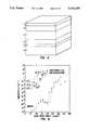
- FIG. 4shows a typical large-area double heterojunction p-i-n device supported by an amorphous substrate in accordance with the present invention
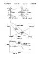
- FIG. 5shows a typical scanning excimer laser irradiation system used in carrying out preferred embodiments of the present invention
- FIG. 6shows a plot of room temperature, dark dc conductivity of excimer laser-scanned (2560 pulses per point) P-doped a-Si:H for various gas-phase impurity mole fractions and undoped a-Si:H as a function of incident laser energy density, with all values normalized to the nominal 150 nm thickness of the initial amorphous layer;
- FIG. 7shows crystallization depth of excimer laser-scanned (2560 pulses per point) 10 -2 P-doped and undoped a-Si:H as a function of incident laser energy density;
- FIG. 8shows a plot of hydrogen concentration versus depth (hydrogen concentration depth profiles) at various laser energy densities for single pulse irradiation, showing that, at higher laser energy densities, the P-doped layer becomes depleted of hydrogen as crystallite formation proceeds;
- FIG. 9shows the room temperature, dark dc conductivity of laser-scanned (512 and 2560 pulses per point) and single-pulse 10 -2 P-doped and undoped a-Si:H as a function of incident laser energy density, with all values normalized to the nominal 150 nm thickness of the initial amorphous layer.
- FIG. 4shows one preferred double heterojunction a-Si:H-based p-i-n device structure.
- the deviceincludes a top contact 1 deposited on a p-type cladding layer 2, an intrinsic or lightly doped middle active layer 3, and an n-type cladding layer 4. Completing this embodiment are bottom contact 5 and amorphous substrate 6.
- the layers 1-6are specifically described hereinafter and in Example 1. It should be pointed out that the type of doping in the layers denoted 2 and 4 may be reversed in physical orientation. Since the diffusion length (average distance that an electron or hole travels in minority regions before combining) is substantially less for holes than for electrons, the preferred structure for detectors has the p-type layer on top (toward the incident radiation), as is known in the art. See for example, Luxon and Parker, Industrial Lasers and Their Applications, Prentice-Hall, Inc., pages 62-67 (1985).
- the top contact 1 and bottom contact 5are preferably chrome or ITO (indium tin oxide), although other electrical conductors, such as aluminum or TCO (transparent conductive oxides) may be used.
- the bottom contact 5is deposited directly onto amorphous substrate 6, via electron beam in the case of ITO, while top contact 1 is deposited directly on top of p-type layer 2.
- the device shown in FIG. 4preferably has hydrogenated a-Si x :C 1-x p- and n-type layers 2 and 4, respectively.
- Other Group IVa elementscan be alloyed with silicon, such as germanium. Carbon and germanium are preferred as they have the same diamond crystal structure as silicon.
- the value of xtypically ranges from about 1.0 to about 0.6, more typically ranging from about 0.9 to about 0.7.
- the intrinsic i-layer 3is shown sandwiched between p- and n- type layers 2 and 4, respectively. This effectively increases the volume of depletion regions formed in a normal pn device.
- the undoped or slightly doped hydrogenated amorphous silicon layer 3has a smaller band gap than the adjoining p- and n- type cladding layers 2 and 4. This was shown in reference to FIG. 3, wherein wide-band gap cladding layers were shown desirable as they allow optical wave guiding, improved recombination efficiency in the active i-layer, and increased LED emission energies from the active i- layer.
- Thickness of the respective layers 2, 3 and 4 shown in FIG. 4may vary or be the same, as a particular device or material constraint allows. In actual usage, there is a compromise between device and material constraints. For surface emitting device structures, efficient performance is seen with intrinsic layers of about 800 ⁇ , with the p- and n-type layers being thicker than this. However, thicknesses in these ranges often require appreciable injection current for radiation emission, or electron-hole recombination. Therefore, for material reasons, thin layers on the order of 100 ⁇ for the active i-layer and 200 ⁇ for the p- and n- cladding layers would appear reasonable.
- i- type layershaving thicknesses ranging from about 350 ⁇ to about 450 ⁇ , with the p- and n-type cladding layers 2 and 4 respectively ranging in thickness from about 150 ⁇ to about 250 ⁇ .
- a device as shown in FIG. 4having amorphous cladding layers 2 and 4 having thicknesses ranging from about 180 ⁇ to about 220 ⁇ , and an intrinsic layer 3 having a thickness ranging from about 375 ⁇ to about 425 ⁇ .
- Different relative thickness rangesmay be appropriate for edge emitting device structures.
- amorphous silicon and its alloysrefers to amorphous silicon alloy films deposited by the RF glow discharge decomposition of pure or dopant-gas-diluted silane or undoped silane onto glass or quartz substrates.
- ion implantationis used to "amorphize” the top surface of a crystalline silicon layer.
- Dopingrefers to introducing impurities, primarily group V elements phosphorus (P), arsenic, and antimony, and the group III element boron (B). The group V elements produce n-type doped layers, while boron produces p-type layers. Doping and hydrogenation can be achieved during the RF glow discharge process.
- Dopingcan also be achieved by ion implantation techniques. See, for example, V.L.S.I. Technology, McGraw-Hill, edited by Sze, pages 107-108, and chapter 6 (1983). However, it may be difficult to achieve desired impurity concentration profiles by ion implantation. Uniform impurity concentrations can be varied controllably over several orders of magnitude in a-Si:H by gas-phase doping. Therefore, hydrogenated amorphous silicon and alloys are preferred.
- alloyrefers to substitutional solid-solution of group IVa elements as discussed, supra.
- Preferred n-type dopantis phosphorus, while boron is the preferred p-type dopant
- One method in accordance with the present inventionincludes increasing the conductivity of p- and n- type hydrogenated amorphous silicon alloys in a p-i-n device as shown in FIG. 4, without substantially affecting the photoconductivity, resistivity, radiation detection, and other properties of the intermediate i-type hydrogenated amorphous silicon layer, by using steps including:
- step (b)forming an intrinsic hydrogenated amorphous silicon layer over the layer of step (a);
- the (a) and (c) cladding layer alloysare preferably silicon alloyed with an element selected from the group consisting of carbon and germanium.
- the preferable heterojunction p-i-n structurehas the p- and n-type layers having identical amount and type of alloy in each layer, although different alloys with differing amounts of alloying element will be appreciated to be within the scope of the present invention.
- a second method in accordance with the present invention of increasing the conductivity of p- and n- type hydrogenated amorphous silicon alloy regions in a p-i-n deviceincludes the steps of:
- step (d)forming a p- or n-type hydrogenated amorphous silicon alloy region doped oppositely from that of step (a) over said i-type region;
- step (e)irradiating said region formed in step (d) with a scanning laser, thereby crystallizing the p- or n- type region to a known degree and increasing the conductivity of the p- or n-type layer without substantially affecting the i-type region.
- a third method in accordance with the present invention of increasing the conductivity and mobility of the p-and n- type hydrogenated amorphous silicon alloy regions in a p-i-n deviceincludes the steps of:
- step (c)forming a hydrogenated amorphous silicon alloy region doped opposite of the layer formed in step (a) over said i-type region;
- the first of the methods of increasing the conductivity of the amorphous cladding layerstakes advantage of the fact that the crystallization rate is greater in doped layers than in the intrinsic or lightly doped middle layer.
- the second method of the inventioncrystallizes the first deposited cladding layer, then deposits the intermediate intrinsic layer on top of the crystallized first cladding layer, and then deposits the second cladding layer on top of the intrinsic layer, and crystallizes this second cladding layer.
- the third methodtakes advantage of "transparent" amorphous substrates which are particularly preferable in the methods of the present invention, wherein the p-i-n device is irradiated from substantially opposite directions, that is, with radiation substantially normal to the top and bottom layers and in opposite directions.
- transparentmeans transparent at least to the incident radiation wavelengths, not necessarily visible wavelengths.
- the scanning radiation source used in the first described methodis preferably a pulse excimer laser with pulse time ranging from about 1 to about 100 nanoseconds.
- the scanning radiation sourcemay also include a continuous wave scanning laser or a broad-band spectral source with a programmable anneal.
- the scanning radiation sourceis a pulsed excimer laser with pulse times ranging from about 10 ns to about 25 ns, scanning at about 512 to about 2560 pulse per point, at a frequency ranging from about 24 to about 40 Hz.
- the wavelength of the scanning excimer laserpreferably ranges from about 155 nm to about 250 nm, depending on the type of excimer laser used.
- the major types of excimer lasersare well known and are given in the following table:
- Most particularly preferred for this inventionis the XeCl excimer laser operating at 308 nm, having a pulse time ranging from about 10 to about 25 nanoseconds.
- the use of an excimer laser facilityis preferable in a research laboratory setting which one day may be working with a 308 nm xenon-chloride line, and the next day may need the 193 nm argon-fluoride wavelength.
- the researcherwould pump out the old gas mixture, passivate the tube to remove contaminants, then pump out that mixture and replace it with the new laser gas mixture.
- This capabilityis not essential for industrial applications, and such lasers are often made for a specific gas mixture. Both the research and industrial-type excimer lasers are considered useful in the present invention.
- FIG. 5shows a schematic of a typical excimer laser facility for scanning crystallization of amorphous silicon alloys.
- Laser 7is positioned so that its beam passes through beam homogenizer 8, which narrows and collimates the beam.
- Typical "before” and “after” beam profilesare shown at 9 and 10, respectively.
- Intensity "I”is plotted qualitatively vs. beam width in millimeters, in profiles 8 and 9. Part of the beam then is reflected by mirror 11 into vacuum chamber 12.
- an x-y stage 13moves substrates 14 so that a scanning beam traverses the substrate, as shown in the enlarged view.
- the laser beamcould move across a stationary substrate, but the embodiment shown is preferred due to optical alignment of laser, homogenizer, etc.
- Further peripheral devicesinclude beam profiler 15 and monitor interface 16, which allow a human operator to view the laser beam shape. As seen in the enlarged view, preferably a square beam spot is used at the plane of focus. Other beam shapes are possible to effect the scan. For example, rectangular, semi-circular, and ellipsoidal shapes may be employed, as well as combinations of these. It is also possible to envision more than one beam type and amount simultaneously or sequentially scanning the substrate. These variations are, of course, considered within the scope and content of the invention.
- Scanningis performed preferably at temperatures ranging from about zero to about 100° C., and at pressures ⁇ about 1 ⁇ 10 -5 torr, at average energy densities ranging from about 50 to about 200 mJ/cm 2 .
- Particularly preferableare methods wherein scanning is performed at about room temperature (i.e., from about 20° C. to about 25° C.) at pressures ⁇ about 1 ⁇ 10 -6 torr, at average energy densities ranging from about 75 to about 200 mJ/cm 2 .
- the room temperature dark dc conductivity of P-doped a-Si:H and its alloysexhibit a well-defined laser energy density threshold (about 85 mJ/cm 2 ) at which the conductivity increases by several orders of magnitude.
- the laser energy density thresholdincreases as the gas phase mole fraction or solid layer mole fraction of dopant decreases.
- Increases in conductivity exhibitedpreferably range from a factor of about 100 to about 10,000 times the conductivity of the originally amorphous layer.
- the conductivityexhibits an increase ranging from a factor of about 100 to about 1000 times the conductivity of the originally amorphous layer.
- the important discoveryis that the increase in conductivity is attained at a known energy density threshold which increases as the dopant concentration in the amorphous silicon alloy decreases.
- Fast-pulse scanning laser annealing of a-Si:H alloysshares all the important advantages of ⁇ c-Si:H, but offers the further advantages of spatial selectivity, the capability of post-deposition processing, and efficient crystallization of amorphous silicon alloys.
- the dc dark conductivity of laser-annealed, highly-doped a-Si:H alloysincreases by a factor of roughly 350 above a sharp laser energy density threshold whose magnitude increases with decreasing impurity concentration and which correlates with the onset of hydrogen evolution from and recrystallization of the near-surface layer.
- a-Si:H films150-nm-thick-high quality a-Si:H films were deposited by the RF glow discharge composition (2 watts, 500K) of phosphine diluted in silane onto 300 nm thick a-SiN x buffer layers supported by glass substrates. The films were scanned at room temperature, under a pressure ⁇ 1 ⁇ 10 -6 torr vacuum, with 512 or 2560 pulse per point at 24 or 40 Hz, with a XeCl excimer laser (308 nm, 17 ns) at average laser energy densities between 60 and 420 mJ/cm 2 .
- Chrome contactswere evaporated onto the resulting films in the gap cell configuration for dc conductivity and in the Van der Pauw configuration for Hall mobility measurements.
- the laser-irradiated a-Si:H filmswere also characterized by Raman spectroscopy, x-ray diffraction, and transmission electron microscopy (TEM) measurements.
- the transport properties of laser-scanned P-doped a-Si:Hare shown in FIG. 6.
- the room temperature dark dc conductivity of 10 -2 P-doped a-Si:Hexhibited a well-defined laser energy density threshold (about 85 mJ/cm 2 ) at which the conductivity increased by several orders of magnitude.
- the laser energy density thresholdincreased as the gas phase P mole fraction decreased. Similar behavior was observed in B-doped a-Si:H.
- the electron Hall mobilities of the P-doped filmsincreased from+(0.01-0.1) to -(1-5) cm 2 /Vs at the same energy density thresholds.
- the sign change of the Hall coefficients at thresholdindicates that an amorphous to crystalline phase change has occurred in the dominating conducting layer.
- the structure of the 10 -2 P-doped a-Si:H filmswas investigated just below, at, and just above the roughly 85 mJ-cm 2 threshold by Raman, x-ray diffraction, and TEM measurements.
- the Raman spectraexhibited the sharp peak near 515 cm -1 characteristic of crystallized silicon only in films just above threshold ( ⁇ 90 mJ/cm 2 ).
- X-ray diffraction resultsshowed essentially the same behavior, with the average grain size increasing from the a-Si:H background at and below threshold to about 3 nm just above threshold.
- TEM micrographsshowed the formation of small (1-2 nm diameter) crystallites distributed discontinuously within the first 4-6 nm of the a-Si:H surface just at threshold (85 mJ/cm 2 ).
- threshold90 mJ per square centimeter
- a continuous surface layer of crystallized a-Si:Hwas formed whose thickness increased with increasing laser energy density.
- the increase in the conductivity near thresholdis, therefore, a percolation phenomena with the large increase in conductivity arising from the formation of a continuous polycrystalline conduction path with correspondingly enhanced mobility and dopant activation.
- the use of the nominal 150 nm film thickness to normalize the conductance in FIG. 6undervalues the conductivity of the dominant conducting layer above threshold. Taking into account the actual thickness of this layer, about 3 nm, in 10 -2 P-doped a-Si:H just above threshold, its conductivity becomes roughly 500 ohm -1 cm -1 . This corresponds to an electron concentration of roughly 1 ⁇ 10 21 cm -3 (compared to roughly 3 ⁇ 10 17 cm -3 in the amorphous phase), which is near the phosphorous solubility limit at the c-Si melt temperature and approaches 100% phosphorous activation.
- the entire a-Si:H filmwas transformed into a continuous, large-grained (about 100 nm diameter) polycrystalline layer above about 400 mJ/cm 2 .
- heterogeneous layersformed composed of large polycrystals near the surface due to regrowth from the melt, which were separated from the remaining amorphous material by a layer of smaller microcrystallites and microvoids characteristic of explosive crystallization.
- the polycrystalline and total crystallized depthshave been interpreted as primary and secondary melt depths, respectively.
- Both the primary and secondary melt depthsincreased rapidly above the laser energy density threshold for enhanced transport in 10 -2 P-doped a-Si:H. Similar behavior was observed in nominally undoped a-Si:H, except that the crystallization thresholds occurred at higher laser energy densities.
- the second conductivity enhancement threshold from about 10 -7 ohm -1 cm -1 at 200 mJ/cm 2 to about 10 -1 ohm -1 cm -1 at 260 mJ/cm 2 in undoped a-Si:H (FIG. 6)is due not to an increase in melt depth, but to an increase in lateral grain growth and grain quality. This was clear from visual inspection of the TEM micrographs; the roughly 10 6 increase in carrier mobility corresponded to a similar decrease in the intergran
- the H concentration depth profiles for single pulse irradiationare shown in FIG. 8. (It should be pointed out that multiple pulses may also be used in these methods.
- a stream of pulsesranging from about 0 to about 200 pulses/sec, preferably ranging from about 20 to about 50 pulses/sec, may be used.
- Pno change in the H concentration depth profile was observed below an energy density of 140 mJ/cm 2 .
- the H concentration near the P-doped/undoped interfacebecame enhanced relative to that in the remaining P-doped layer.
- the P-doped layerbecame increasingly depleted of H as crystallite formation proceeded.
- H depletion of the near-surfaceclearly accompanied large grain polycrystallite formation.
- TEM micrographsshowed that the microcrystalline layer between the polycrystalline near-surface and the amorphous bulk contained a large concentration of microvoids, which most likely resulted from H 2 gas bubble formation.
- the polycrystalline layercan only increase in thickness if H in this defective microcrystalline layer can diffuse through the polycrystalline/melt region and escape to the vacuum during laser annealing.
- FIG. 9The effects of laser scanning compared to single laser pulse irradiation on the crystallization threshold are shown in FIG. 9.
- Sharp laser energy density thresholds for primary meltingoccurred at about 120 to about 140 mJ/cm 2 for undoped a-Si:H, and about 90 to about 100 mJ/cm 2 10 -2 for P-doped are observed at scanning densities of both 2560 and 512 shots per point.
- the thresholds for a single-pulse irradiationare also sharp, but both occurred at 200 mJ/cm 2 , near the laser energy density where significant lateral grain growth in undoped a-Si:H began under scanned conditions. There appears to be no melt threshold reduction due to doping in the single pulse case.
Landscapes
- Recrystallisation Techniques (AREA)
- Led Devices (AREA)
- Thin Film Transistor (AREA)
- Photovoltaic Devices (AREA)
- Light Receiving Elements (AREA)
Abstract
Description
TABLE I* ______________________________________ Type Wavelength (nm) ______________________________________ F.sub.2 157 ArF 193 KrCl 222 KrF 249 XeCl 308XeF 350 ______________________________________ *From Understanding Lasers, Hecht, page 214 (Howard W. Sams & Company, publisher, 1988).
Claims (33)
Priority Applications (3)
| Application Number | Priority Date | Filing Date | Title |
|---|---|---|---|
| US07/634,896US5162239A (en) | 1990-12-27 | 1990-12-27 | Laser crystallized cladding layers for improved amorphous silicon light-emitting diodes and radiation sensors |
| JP3338923AJPH04302136A (en) | 1990-12-27 | 1991-12-20 | Improved method for forming laser crystallized cladding layers for amorphous silicon light emitting diodes and radiation sensors |
| US07/866,737US5210766A (en) | 1990-12-27 | 1992-04-10 | Laser crystallized cladding layers for improved amorphous silicon light-emitting diodes and radiation sensors |
Applications Claiming Priority (1)
| Application Number | Priority Date | Filing Date | Title |
|---|---|---|---|
| US07/634,896US5162239A (en) | 1990-12-27 | 1990-12-27 | Laser crystallized cladding layers for improved amorphous silicon light-emitting diodes and radiation sensors |
Related Child Applications (1)
| Application Number | Title | Priority Date | Filing Date |
|---|---|---|---|
| US07/866,737DivisionUS5210766A (en) | 1990-12-27 | 1992-04-10 | Laser crystallized cladding layers for improved amorphous silicon light-emitting diodes and radiation sensors |
Publications (1)
| Publication Number | Publication Date |
|---|---|
| US5162239Atrue US5162239A (en) | 1992-11-10 |
Family
ID=24545588
Family Applications (1)
| Application Number | Title | Priority Date | Filing Date |
|---|---|---|---|
| US07/634,896Expired - Fee RelatedUS5162239A (en) | 1990-12-27 | 1990-12-27 | Laser crystallized cladding layers for improved amorphous silicon light-emitting diodes and radiation sensors |
Country Status (2)
| Country | Link |
|---|---|
| US (1) | US5162239A (en) |
| JP (1) | JPH04302136A (en) |
Cited By (26)
| Publication number | Priority date | Publication date | Assignee | Title |
|---|---|---|---|---|
| US5366926A (en)* | 1993-06-07 | 1994-11-22 | Xerox Corporation | Low temperature process for laser dehydrogenation and crystallization of amorphous silicon |
| US5930608A (en)* | 1992-02-21 | 1999-07-27 | Semiconductor Energy Laboratory Co., Ltd. | Method of fabricating a thin film transistor in which the channel region of the transistor consists of two portions of differing crystallinity |
| EP0860885A3 (en)* | 1997-02-19 | 2000-05-03 | Canon Kabushiki Kaisha | Photovoltaic device, photoelectric transducer and method of manufacturing same |
| US6071765A (en)* | 1993-11-02 | 2000-06-06 | Sony Corporation | Method of forming polycrystalline silicon layer on substrate and surface treatment apparatus thereof |
| US6210996B1 (en)* | 1995-01-13 | 2001-04-03 | Semiconductor Energy Laboratory Co., Ltd. | Laser illumination system |
| US6297135B1 (en) | 1997-01-29 | 2001-10-02 | Ultratech Stepper, Inc. | Method for forming silicide regions on an integrated device |
| US6323069B1 (en) | 1992-03-25 | 2001-11-27 | Semiconductor Energy Laboratory Co., Ltd. | Method of manufacturing a thin film transistor using light irradiation to form impurity regions |
| US6331717B1 (en) | 1993-08-12 | 2001-12-18 | Semiconductor Energy Laboratory Co. Ltd. | Insulated gate semiconductor device and process for fabricating the same |
| WO2001073857A3 (en)* | 2000-03-27 | 2002-01-31 | Aegis Semiconductor | A semitransparent optical detector including a polycrystalline layer and method of making |
| WO2001071820A3 (en)* | 2000-03-27 | 2002-02-14 | Aegis Semiconductor | A semitransparent optical detector with a transparent conductor and method of making |
| US6387803B2 (en) | 1997-01-29 | 2002-05-14 | Ultratech Stepper, Inc. | Method for forming a silicide region on a silicon body |
| US6458200B1 (en)* | 1990-06-01 | 2002-10-01 | Semiconductor Energy Laboratory Co., Ltd. | Method for fabricating thin-film transistor |
| US20020145139A1 (en)* | 2000-03-20 | 2002-10-10 | Sigurd Wagner | Semitransparent optical detector including a polycrystalline layer and method of making |
| US6500703B1 (en) | 1993-08-12 | 2002-12-31 | Semicondcutor Energy Laboratory Co., Ltd. | Insulated gate semiconductor device and process for fabricating the same |
| US20030032222A1 (en)* | 1999-07-22 | 2003-02-13 | Nec Corporation | Pulse laser irradation method for forming a semiconductor thin film |
| US20030072009A1 (en)* | 2001-08-02 | 2003-04-17 | Domash Lawrence H. | Tunable optical instruments |
| US6670599B2 (en) | 2000-03-27 | 2003-12-30 | Aegis Semiconductor, Inc. | Semitransparent optical detector on a flexible substrate and method of making |
| US20050030628A1 (en)* | 2003-06-20 | 2005-02-10 | Aegis Semiconductor | Very low cost narrow band infrared sensor |
| US20050074206A1 (en)* | 2003-09-08 | 2005-04-07 | Aegis Semiconductor, Inc. | Tunable dispersion compensator |
| US20050082480A1 (en)* | 2003-08-26 | 2005-04-21 | Aegis Semiconductor, Inc. | Infrared camera system |
| US20050105185A1 (en)* | 2003-10-07 | 2005-05-19 | Aegis Semiconductor, Inc | Tunable optical filter with heater on a CTE-matched transparent substrate |
| CN1314080C (en)* | 1993-01-18 | 2007-05-02 | 株式会社半导体能源研究所 | Manufacturing method of MIS semiconductor device |
| US20070117287A1 (en)* | 2005-11-23 | 2007-05-24 | Semiconductor Energy Laboratory Co., Ltd. | Laser irradiation apparatus |
| US20130017674A1 (en)* | 2011-07-13 | 2013-01-17 | Toshiba America Electronic Components, Inc. | Cryogenic silicon ion-implantation and recrystallization annealing |
| US11666987B2 (en)* | 2018-03-13 | 2023-06-06 | Sumitomo Heavy Industries, Ltd. | Laser power control device, laser machining device, and laser power control method |
| CN118676249A (en)* | 2024-05-31 | 2024-09-20 | 淮安捷泰新能源科技有限公司 | Preparation method of TOPCon battery and TOPCon battery |
Families Citing this family (1)
| Publication number | Priority date | Publication date | Assignee | Title |
|---|---|---|---|---|
| KR100768414B1 (en)* | 2000-03-13 | 2007-10-18 | 소니 가부시끼 가이샤 | Optical energy converter |
Citations (13)
| Publication number | Priority date | Publication date | Assignee | Title |
|---|---|---|---|---|
| JPS5961138A (en)* | 1982-09-30 | 1984-04-07 | Fujitsu Ltd | Manufacturing method of semiconductor device |
| US4525375A (en)* | 1983-03-28 | 1985-06-25 | Rca Corporation | Method of controllong the deposition of hydrogenated amorphous silicon and apparatus therefor |
| US4528082A (en)* | 1983-09-26 | 1985-07-09 | Exxon Research And Engineering Co. | Method for sputtering a PIN amorphous silicon semi-conductor device having partially crystallized P and N-layers |
| JPS61160979A (en)* | 1985-01-08 | 1986-07-21 | Sharp Corp | Manufacture of amorphous solar cell |
| US4609407A (en)* | 1979-11-21 | 1986-09-02 | Hitachi, Ltd. | Method of making three dimensional semiconductor devices in selectively laser regrown polysilicon or amorphous silicon layers |
| US4624862A (en)* | 1984-11-05 | 1986-11-25 | Energy Conversion Devices, Inc. | Boron doped semiconductor materials and method for producing same |
| US4718947A (en)* | 1986-04-17 | 1988-01-12 | Solarex Corporation | Superlattice doped layers for amorphous silicon photovoltaic cells |
| JPS6441278A (en)* | 1987-08-07 | 1989-02-13 | Fuji Electric Co Ltd | Manufacture of thin film photovoltaic element |
| US4845043A (en)* | 1987-04-23 | 1989-07-04 | Catalano Anthony W | Method for fabricating photovoltaic device having improved short wavelength photoresponse |
| US4891330A (en)* | 1987-07-27 | 1990-01-02 | Energy Conversion Devices, Inc. | Method of fabricating n-type and p-type microcrystalline semiconductor alloy material including band gap widening elements |
| US4910153A (en)* | 1986-02-18 | 1990-03-20 | Solarex Corporation | Deposition feedstock and dopant materials useful in the fabrication of hydrogenated amorphous silicon alloys for photovoltaic devices and other semiconductor devices |
| JPH02122574A (en)* | 1988-10-31 | 1990-05-10 | Kyocera Corp | Manufacturing method of photoelectric conversion device |
| US5055416A (en)* | 1988-12-07 | 1991-10-08 | Minnesota Mining And Manufacturing Company | Electrolytic etch for preventing electrical shorts in solar cells on polymer surfaces |
- 1990
- 1990-12-27USUS07/634,896patent/US5162239A/ennot_activeExpired - Fee Related
- 1991
- 1991-12-20JPJP3338923Apatent/JPH04302136A/ennot_activeWithdrawn
Patent Citations (13)
| Publication number | Priority date | Publication date | Assignee | Title |
|---|---|---|---|---|
| US4609407A (en)* | 1979-11-21 | 1986-09-02 | Hitachi, Ltd. | Method of making three dimensional semiconductor devices in selectively laser regrown polysilicon or amorphous silicon layers |
| JPS5961138A (en)* | 1982-09-30 | 1984-04-07 | Fujitsu Ltd | Manufacturing method of semiconductor device |
| US4525375A (en)* | 1983-03-28 | 1985-06-25 | Rca Corporation | Method of controllong the deposition of hydrogenated amorphous silicon and apparatus therefor |
| US4528082A (en)* | 1983-09-26 | 1985-07-09 | Exxon Research And Engineering Co. | Method for sputtering a PIN amorphous silicon semi-conductor device having partially crystallized P and N-layers |
| US4624862A (en)* | 1984-11-05 | 1986-11-25 | Energy Conversion Devices, Inc. | Boron doped semiconductor materials and method for producing same |
| JPS61160979A (en)* | 1985-01-08 | 1986-07-21 | Sharp Corp | Manufacture of amorphous solar cell |
| US4910153A (en)* | 1986-02-18 | 1990-03-20 | Solarex Corporation | Deposition feedstock and dopant materials useful in the fabrication of hydrogenated amorphous silicon alloys for photovoltaic devices and other semiconductor devices |
| US4718947A (en)* | 1986-04-17 | 1988-01-12 | Solarex Corporation | Superlattice doped layers for amorphous silicon photovoltaic cells |
| US4845043A (en)* | 1987-04-23 | 1989-07-04 | Catalano Anthony W | Method for fabricating photovoltaic device having improved short wavelength photoresponse |
| US4891330A (en)* | 1987-07-27 | 1990-01-02 | Energy Conversion Devices, Inc. | Method of fabricating n-type and p-type microcrystalline semiconductor alloy material including band gap widening elements |
| JPS6441278A (en)* | 1987-08-07 | 1989-02-13 | Fuji Electric Co Ltd | Manufacture of thin film photovoltaic element |
| JPH02122574A (en)* | 1988-10-31 | 1990-05-10 | Kyocera Corp | Manufacturing method of photoelectric conversion device |
| US5055416A (en)* | 1988-12-07 | 1991-10-08 | Minnesota Mining And Manufacturing Company | Electrolytic etch for preventing electrical shorts in solar cells on polymer surfaces |
Non-Patent Citations (18)
| Title |
|---|
| Fang, P. H., "Excimer-Laser-Induced Silicon Amorphous-Microcrystalline Transformation and its Solar Cell Applications", Solar Cells, vol. 25, pp. 27-29 (1988). |
| Fang, P. H., Excimer Laser Induced Silicon Amorphous Microcrystalline Transformation and its Solar Cell Applications , Solar Cells, vol. 25, pp. 27 29 (1988).* |
| Hamakawa et al., "Optoelectronics and Photovoltaic Applications of Microcrystalline SiC", presented at the Materials Research Society Symposium proceedings, Nov. 27, 1989. |
| Hamakawa et al., Optoelectronics and Photovoltaic Applications of Microcrystalline SiC , presented at the Materials Research Society Symposium proceedings, Nov. 27, 1989.* |
| Kruangam et al., "Amorphous-Silicon-Carbide Thin Film Light-Emitting Diode", Optoelectronics-Devices and Technologies, vol. 1, No. 1, pp. 67-84, Jun., 1986. |
| Kruangam et al., Amorphous Silicon Carbide Thin Film Light Emitting Diode , Optoelectronics Devices and Technologies, vol. 1, No. 1, pp. 67 84, Jun., 1986.* |
| Sclater, "Gallium Arsenide IC Technology", TAB Professional and Reference Books, Blue Ridge Summit, Pa., Chapters 1 and 2 (1988). |
| Sclater, Gallium Arsenide IC Technology , TAB Professional and Reference Books, Blue Ridge Summit, Pa., Chapters 1 and 2 (1988).* |
| Siebert et al., "Photoluminescence in a-Si1-x Cx :H Films", Phys. Stat. Sol., (b) 140, 311 (1987). |
| Siebert et al., Photoluminescence in a Si 1 x C x :H Films , Phys. Stat. Sol., (b) 140, 311 (1987).* |
| Street, "Luminescence in a-Si:H", Semiconductors and Semimetals, vol. 21, Part B, pp. 197-244 (1984). |
| Street, Luminescence in a Si:H , Semiconductors and Semimetals, vol. 21, Part B, pp. 197 244 (1984).* |
| Winer et al., "Excimer-Laser-Induced Crystallization of Hydrogenated Amorphous Silicon", Appl. Phys. Lett., 57, No. 21; Nov. 19, 1990; pp. 2222-2224. |
| Winer et al., "Fast-Pulse Excimer-Laser-Induced Processes in a-Si:H", presented at the Materials Research Society Symposium proceedings, Nov. 27, 1989. |
| Winer et al., "Universal Dopant and Defect Equilibrium Kinetics in n-type a-Si:H", Physical Review B, vol. 40, No. 18, Dec. 15, 1989, pp. 12558-12561. |
| Winer et al., Excimer Laser Induced Crystallization of Hydrogenated Amorphous Silicon , Appl. Phys. Lett., 57, No. 21; Nov. 19, 1990; pp. 2222 2224.* |
| Winer et al., Fast Pulse Excimer Laser Induced Processes in a Si:H , presented at the Materials Research Society Symposium proceedings, Nov. 27, 1989.* |
| Winer et al., Universal Dopant and Defect Equilibrium Kinetics in n type a Si:H , Physical Review B, vol. 40, No. 18, Dec. 15, 1989, pp. 12558 12561.* |
Cited By (46)
| Publication number | Priority date | Publication date | Assignee | Title |
|---|---|---|---|---|
| US6458200B1 (en)* | 1990-06-01 | 2002-10-01 | Semiconductor Energy Laboratory Co., Ltd. | Method for fabricating thin-film transistor |
| US7018874B2 (en) | 1990-06-01 | 2006-03-28 | Semiconductor Energy Laboratory Co., Ltd. | Method for fabricating thin-film transistor |
| US6740547B2 (en) | 1990-06-01 | 2004-05-25 | Semiconductor Energy Laboratory Co., Ltd. | Method for fabricating thin-film transistor |
| US6717180B2 (en) | 1991-02-22 | 2004-04-06 | Semiconductor Energy Laboratory Co., Ltd. | Semiconductor device and method for forming the same |
| US6352883B1 (en) | 1991-02-22 | 2002-03-05 | Semiconductor Energy Laboratory Co., Ltd. | Semiconductor device and method for forming the same |
| US5930608A (en)* | 1992-02-21 | 1999-07-27 | Semiconductor Energy Laboratory Co., Ltd. | Method of fabricating a thin film transistor in which the channel region of the transistor consists of two portions of differing crystallinity |
| US6323069B1 (en) | 1992-03-25 | 2001-11-27 | Semiconductor Energy Laboratory Co., Ltd. | Method of manufacturing a thin film transistor using light irradiation to form impurity regions |
| US6569724B2 (en) | 1992-03-25 | 2003-05-27 | Semiconductor Energy Laboratory Co., Ltd. | Insulated gate field effect transistor and method for forming the same |
| US6887746B2 (en) | 1992-03-25 | 2005-05-03 | Semiconductor Energy Lab | Insulated gate field effect transistor and method for forming the same |
| CN1314080C (en)* | 1993-01-18 | 2007-05-02 | 株式会社半导体能源研究所 | Manufacturing method of MIS semiconductor device |
| US5366926A (en)* | 1993-06-07 | 1994-11-22 | Xerox Corporation | Low temperature process for laser dehydrogenation and crystallization of amorphous silicon |
| US7381598B2 (en) | 1993-08-12 | 2008-06-03 | Semiconductor Energy Laboratory Co., Ltd. | Insulated gate semiconductor device and process for fabricating the same |
| US6500703B1 (en) | 1993-08-12 | 2002-12-31 | Semicondcutor Energy Laboratory Co., Ltd. | Insulated gate semiconductor device and process for fabricating the same |
| US6331717B1 (en) | 1993-08-12 | 2001-12-18 | Semiconductor Energy Laboratory Co. Ltd. | Insulated gate semiconductor device and process for fabricating the same |
| US6437366B1 (en) | 1993-08-12 | 2002-08-20 | Semiconductor Energy Laboratory Co., Ltd. | Insulated gate semiconductor device and process for fabricating the same |
| US6071765A (en)* | 1993-11-02 | 2000-06-06 | Sony Corporation | Method of forming polycrystalline silicon layer on substrate and surface treatment apparatus thereof |
| US6706570B2 (en) | 1995-01-13 | 2004-03-16 | Semiconductor Energy Laboratory Co., Ltd., | Laser illumination system |
| US7528079B2 (en) | 1995-01-13 | 2009-05-05 | Semiconductor Energy Laboratory Co., Ltd. | Method of changing an energy attenuation factor of a linear light in order to crystallize a semiconductor film |
| US6784030B2 (en) | 1995-01-13 | 2004-08-31 | Semiconductor Energy Laboratory Co., Ltd. | Laser illumination system |
| US6468842B2 (en) | 1995-01-13 | 2002-10-22 | Semiconductor Energy Laboratory Co., Ltd. | Laser illumination system |
| US6210996B1 (en)* | 1995-01-13 | 2001-04-03 | Semiconductor Energy Laboratory Co., Ltd. | Laser illumination system |
| US6387803B2 (en) | 1997-01-29 | 2002-05-14 | Ultratech Stepper, Inc. | Method for forming a silicide region on a silicon body |
| US6297135B1 (en) | 1997-01-29 | 2001-10-02 | Ultratech Stepper, Inc. | Method for forming silicide regions on an integrated device |
| EP0860885A3 (en)* | 1997-02-19 | 2000-05-03 | Canon Kabushiki Kaisha | Photovoltaic device, photoelectric transducer and method of manufacturing same |
| US20030032222A1 (en)* | 1999-07-22 | 2003-02-13 | Nec Corporation | Pulse laser irradation method for forming a semiconductor thin film |
| US6800541B2 (en)* | 1999-07-22 | 2004-10-05 | Nec Corporation | Pulse laser irradiation method for forming a semiconductor thin film |
| US20020145139A1 (en)* | 2000-03-20 | 2002-10-10 | Sigurd Wagner | Semitransparent optical detector including a polycrystalline layer and method of making |
| US6879014B2 (en) | 2000-03-20 | 2005-04-12 | Aegis Semiconductor, Inc. | Semitransparent optical detector including a polycrystalline layer and method of making |
| WO2001071820A3 (en)* | 2000-03-27 | 2002-02-14 | Aegis Semiconductor | A semitransparent optical detector with a transparent conductor and method of making |
| US6670599B2 (en) | 2000-03-27 | 2003-12-30 | Aegis Semiconductor, Inc. | Semitransparent optical detector on a flexible substrate and method of making |
| WO2001073857A3 (en)* | 2000-03-27 | 2002-01-31 | Aegis Semiconductor | A semitransparent optical detector including a polycrystalline layer and method of making |
| US7002697B2 (en) | 2001-08-02 | 2006-02-21 | Aegis Semiconductor, Inc. | Tunable optical instruments |
| US20030072009A1 (en)* | 2001-08-02 | 2003-04-17 | Domash Lawrence H. | Tunable optical instruments |
| US20050030628A1 (en)* | 2003-06-20 | 2005-02-10 | Aegis Semiconductor | Very low cost narrow band infrared sensor |
| US20050082480A1 (en)* | 2003-08-26 | 2005-04-21 | Aegis Semiconductor, Inc. | Infrared camera system |
| US20070023661A1 (en)* | 2003-08-26 | 2007-02-01 | Redshift Systems Corporation | Infrared camera system |
| US20050074206A1 (en)* | 2003-09-08 | 2005-04-07 | Aegis Semiconductor, Inc. | Tunable dispersion compensator |
| US7221827B2 (en) | 2003-09-08 | 2007-05-22 | Aegis Semiconductor, Inc. | Tunable dispersion compensator |
| US20050105185A1 (en)* | 2003-10-07 | 2005-05-19 | Aegis Semiconductor, Inc | Tunable optical filter with heater on a CTE-matched transparent substrate |
| US7304799B2 (en) | 2003-10-07 | 2007-12-04 | Aegis Lightwave, Inc. | Tunable optical filter with heater on a CTE-matched transparent substrate |
| US20070117288A1 (en)* | 2005-11-23 | 2007-05-24 | Hidekazu Miyairi | Laser irradiation apparatus |
| US20070117287A1 (en)* | 2005-11-23 | 2007-05-24 | Semiconductor Energy Laboratory Co., Ltd. | Laser irradiation apparatus |
| US7714251B2 (en) | 2005-11-23 | 2010-05-11 | Semiconductor Energy Laboratory Co., Ltd | Laser irradiation apparatus |
| US20130017674A1 (en)* | 2011-07-13 | 2013-01-17 | Toshiba America Electronic Components, Inc. | Cryogenic silicon ion-implantation and recrystallization annealing |
| US11666987B2 (en)* | 2018-03-13 | 2023-06-06 | Sumitomo Heavy Industries, Ltd. | Laser power control device, laser machining device, and laser power control method |
| CN118676249A (en)* | 2024-05-31 | 2024-09-20 | 淮安捷泰新能源科技有限公司 | Preparation method of TOPCon battery and TOPCon battery |
Also Published As
| Publication number | Publication date |
|---|---|
| JPH04302136A (en) | 1992-10-26 |
Similar Documents
| Publication | Publication Date | Title |
|---|---|---|
| US5162239A (en) | Laser crystallized cladding layers for improved amorphous silicon light-emitting diodes and radiation sensors | |
| US5210766A (en) | Laser crystallized cladding layers for improved amorphous silicon light-emitting diodes and radiation sensors | |
| US5627081A (en) | Method for processing silicon solar cells | |
| US5221365A (en) | Photovoltaic cell and method of manufacturing polycrystalline semiconductive film | |
| US9812599B2 (en) | Method of stabilizing hydrogenated amorphous silicon and amorphous hydrogenated silicon alloys | |
| US4400409A (en) | Method of making p-doped silicon films | |
| US20080295882A1 (en) | Photovoltaic device and method of manufacturing photovoltaic devices | |
| EP0763858A2 (en) | Photovoltaic element array and method of fabricating the same | |
| EP0949685A2 (en) | Semiconductor element and its manufacturing method | |
| WO1993012537A1 (en) | High quality photovoltaic semiconductor material and laser ablation method of fabricating same | |
| US4520380A (en) | Amorphous semiconductors equivalent to crystalline semiconductors | |
| EP0656664A1 (en) | Polycrystalline silicon photoelectric transducer and process for its production | |
| Fırat et al. | Industrial metallization of fired passivating contacts for n-type tunnel oxide passivated contact (n-TOPCon) solar cells | |
| US4710786A (en) | Wide band gap semiconductor alloy material | |
| US4677738A (en) | Method of making a photovoltaic panel | |
| JP2004273887A (en) | Crystal thin film semiconductor device and solar cell element | |
| JP2001156026A (en) | Semiconductor elements and manufacturing method therefor | |
| US4839312A (en) | Fluorinated precursors from which to fabricate amorphous semiconductor material | |
| Krivyakin et al. | Optical properties of p–i–n structures based on amorphous hydrogenated silicon with silicon nanocrystals formed via nanosecond laser annealing | |
| US4703336A (en) | Photodetection and current control devices | |
| JP2698115B2 (en) | Method for manufacturing photovoltaic device | |
| Tsuo et al. | High-flux solar furnace processing of silicon solar cells | |
| RU2660220C2 (en) | Method for increasing efficiency of doping and changing conductivity type of amorphous hydrogenated silicon slightly doped with acceptor impurities | |
| JPH11266030A (en) | Semiconductor device and method of manufacturing semiconductor device | |
| Winer et al. | Fast-Pulse Excimer-Laser-Induced Processes in a-Si: H |
Legal Events
| Date | Code | Title | Description |
|---|---|---|---|
| AS | Assignment | Owner name:XEROX CORPORATION, STAMFORD, FAIRFIELD, CONNECTICU Free format text:ASSIGNMENT OF ASSIGNORS INTEREST.;ASSIGNORS:WINER, KRIS A.;THORNTON, ROBERT L.;REEL/FRAME:005651/0136;SIGNING DATES FROM 19910207 TO 19910215 | |
| FEPP | Fee payment procedure | Free format text:PAYOR NUMBER ASSIGNED (ORIGINAL EVENT CODE: ASPN); ENTITY STATUS OF PATENT OWNER: LARGE ENTITY | |
| FPAY | Fee payment | Year of fee payment:4 | |
| FPAY | Fee payment | Year of fee payment:8 | |
| AS | Assignment | Owner name:BANK ONE, NA, AS ADMINISTRATIVE AGENT, ILLINOIS Free format text:SECURITY INTEREST;ASSIGNOR:XEROX CORPORATION;REEL/FRAME:013153/0001 Effective date:20020621 | |
| AS | Assignment | Owner name:JPMORGAN CHASE BANK, AS COLLATERAL AGENT, TEXAS Free format text:SECURITY AGREEMENT;ASSIGNOR:XEROX CORPORATION;REEL/FRAME:015134/0476 Effective date:20030625 Owner name:JPMORGAN CHASE BANK, AS COLLATERAL AGENT,TEXAS Free format text:SECURITY AGREEMENT;ASSIGNOR:XEROX CORPORATION;REEL/FRAME:015134/0476 Effective date:20030625 | |
| REMI | Maintenance fee reminder mailed | ||
| LAPS | Lapse for failure to pay maintenance fees | ||
| STCH | Information on status: patent discontinuation | Free format text:PATENT EXPIRED DUE TO NONPAYMENT OF MAINTENANCE FEES UNDER 37 CFR 1.362 | |
| FP | Lapsed due to failure to pay maintenance fee | Effective date:20041110 | |
| AS | Assignment | Owner name:XEROX CORPORATION, CONNECTICUT Free format text:RELEASE BY SECURED PARTY;ASSIGNOR:JPMORGAN CHASE BANK, N.A. AS SUCCESSOR-IN-INTEREST ADMINISTRATIVE AGENT AND COLLATERAL AGENT TO JPMORGAN CHASE BANK;REEL/FRAME:066728/0193 Effective date:20220822 |