US5161093A - Multiple lamination high density interconnect process and structure employing a variable crosslinking adhesive - Google Patents
Multiple lamination high density interconnect process and structure employing a variable crosslinking adhesiveDownload PDFInfo
- Publication number
- US5161093A US5161093AUS07/546,959US54695990AUS5161093AUS 5161093 AUS5161093 AUS 5161093AUS 54695990 AUS54695990 AUS 54695990AUS 5161093 AUS5161093 AUS 5161093A
- Authority
- US
- United States
- Prior art keywords
- layer
- high density
- density interconnect
- dielectric
- interconnect structure
- Prior art date
- Legal status (The legal status is an assumption and is not a legal conclusion. Google has not performed a legal analysis and makes no representation as to the accuracy of the status listed.)
- Expired - Lifetime
Links
- 239000000853adhesiveSubstances0.000titleclaimsabstractdescription64
- 230000001070adhesive effectEffects0.000titleclaimsabstractdescription64
- 238000004132cross linkingMethods0.000titleclaimsabstractdescription28
- 238000003475laminationMethods0.000titleabstractdescription38
- 238000000034methodMethods0.000titledescription61
- 230000008569processEffects0.000titledescription34
- 239000004593EpoxySubstances0.000claimsabstractdescription52
- 239000000203mixtureSubstances0.000claimsabstractdescription47
- 229920001577copolymerPolymers0.000claimsabstractdescription20
- 238000001465metallisationMethods0.000claimsdescription91
- 229920001187thermosetting polymerPolymers0.000claimsdescription47
- 229920001169thermoplasticPolymers0.000claimsdescription44
- 239000004416thermosoftening plasticSubstances0.000claimsdescription42
- 239000003989dielectric materialSubstances0.000claimsdescription32
- 238000010030laminatingMethods0.000claimsdescription26
- 229920001721polyimidePolymers0.000claimsdescription25
- 239000004642PolyimideSubstances0.000claimsdescription23
- 239000004020conductorSubstances0.000claimsdescription23
- 238000004519manufacturing processMethods0.000claimsdescription18
- 229920000642polymerPolymers0.000claimsdescription15
- 230000002411adverseEffects0.000claimsdescription13
- 239000004697PolyetherimideSubstances0.000claimsdescription11
- 229920001601polyetherimidePolymers0.000claimsdescription11
- 230000009477glass transitionEffects0.000claimsdescription9
- 239000004065semiconductorSubstances0.000claimsdescription9
- 230000006872improvementEffects0.000claimsdescription8
- 238000001035dryingMethods0.000claimsdescription6
- 239000004634thermosetting polymerSubstances0.000claims9
- 239000010410layerSubstances0.000description183
- 239000000758substrateSubstances0.000description43
- 239000000463materialSubstances0.000description30
- 229920003223poly(pyromellitimide-1,4-diphenyl ether)Polymers0.000description16
- 239000002904solventSubstances0.000description14
- 229920004747ULTEM® 1000Polymers0.000description10
- 239000012790adhesive layerSubstances0.000description10
- 229920005989resinPolymers0.000description9
- 239000011347resinSubstances0.000description9
- 230000015572biosynthetic processEffects0.000description8
- 238000004806packaging method and processMethods0.000description8
- 230000008439repair processEffects0.000description8
- 238000001020plasma etchingMethods0.000description7
- 229920004738ULTEM®Polymers0.000description6
- 238000005553drillingMethods0.000description6
- 230000008901benefitEffects0.000description5
- 238000000151depositionMethods0.000description5
- 238000013461designMethods0.000description5
- 238000010438heat treatmentMethods0.000description5
- 239000002861polymer materialSubstances0.000description5
- 238000009987spinningMethods0.000description5
- 238000012360testing methodMethods0.000description5
- KPUWHANPEXNPJT-UHFFFAOYSA-NdisiloxaneChemical class[SiH3]O[SiH3]KPUWHANPEXNPJT-UHFFFAOYSA-N0.000description4
- 230000000694effectsEffects0.000description4
- 238000012545processingMethods0.000description4
- 239000012815thermoplastic materialSubstances0.000description4
- 230000005540biological transmissionEffects0.000description3
- 230000008859changeEffects0.000description3
- 230000006378damageEffects0.000description3
- 230000003247decreasing effectEffects0.000description3
- 230000008021depositionEffects0.000description3
- 125000003700epoxy groupChemical group0.000description3
- 238000001704evaporationMethods0.000description3
- 239000012530fluidSubstances0.000description3
- 238000003801millingMethods0.000description3
- 238000000059patterningMethods0.000description3
- 229920000647polyepoxidePolymers0.000description3
- NIXOWILDQLNWCW-UHFFFAOYSA-MAcrylateChemical compound[O-]C(=O)C=CNIXOWILDQLNWCW-UHFFFAOYSA-M0.000description2
- IJGRMHOSHXDMSA-UHFFFAOYSA-NAtomic nitrogenChemical compoundN#NIJGRMHOSHXDMSA-UHFFFAOYSA-N0.000description2
- CTQNGGLPUBDAKN-UHFFFAOYSA-NO-XyleneChemical compoundCC1=CC=CC=C1CCTQNGGLPUBDAKN-UHFFFAOYSA-N0.000description2
- XUIMIQQOPSSXEZ-UHFFFAOYSA-NSiliconChemical compound[Si]XUIMIQQOPSSXEZ-UHFFFAOYSA-N0.000description2
- 230000003044adaptive effectEffects0.000description2
- 239000000919ceramicSubstances0.000description2
- 239000011248coating agentSubstances0.000description2
- 238000000576coating methodMethods0.000description2
- SBZXBUIDTXKZTM-UHFFFAOYSA-NdiglymeChemical compoundCOCCOCCOCSBZXBUIDTXKZTM-UHFFFAOYSA-N0.000description2
- 230000008020evaporationEffects0.000description2
- 230000005251gamma rayEffects0.000description2
- 238000001459lithographyMethods0.000description2
- 239000000155meltSubstances0.000description2
- 230000008018meltingEffects0.000description2
- 238000002844meltingMethods0.000description2
- 239000002184metalSubstances0.000description2
- 229910052751metalInorganic materials0.000description2
- 238000012986modificationMethods0.000description2
- 230000004048modificationEffects0.000description2
- 229920002120photoresistant polymerPolymers0.000description2
- 238000002360preparation methodMethods0.000description2
- 230000005855radiationEffects0.000description2
- 229910052710siliconInorganic materials0.000description2
- 239000010703siliconSubstances0.000description2
- 239000007787solidSubstances0.000description2
- 230000004580weight lossEffects0.000description2
- 239000008096xyleneSubstances0.000description2
- -1(phenyl) iodonium hexafluoroantimonateChemical compound0.000description1
- 238000003855Adhesive LaminationMethods0.000description1
- RYGMFSIKBFXOCR-UHFFFAOYSA-NCopperChemical compound[Cu]RYGMFSIKBFXOCR-UHFFFAOYSA-N0.000description1
- 241001441571HiodontidaeSpecies0.000description1
- OWYWGLHRNBIFJP-UHFFFAOYSA-NIpazineChemical compoundCCN(CC)C1=NC(Cl)=NC(NC(C)C)=N1OWYWGLHRNBIFJP-UHFFFAOYSA-N0.000description1
- 238000002679ablationMethods0.000description1
- 150000001252acrylic acid derivativesChemical class0.000description1
- 239000012190activatorSubstances0.000description1
- 230000001464adherent effectEffects0.000description1
- PNEYBMLMFCGWSK-UHFFFAOYSA-Naluminium oxideInorganic materials[O-2].[O-2].[O-2].[Al+3].[Al+3]PNEYBMLMFCGWSK-UHFFFAOYSA-N0.000description1
- 238000013459approachMethods0.000description1
- 230000000712assemblyEffects0.000description1
- 238000000429assemblyMethods0.000description1
- 230000009286beneficial effectEffects0.000description1
- 239000003054catalystSubstances0.000description1
- 238000006243chemical reactionMethods0.000description1
- 239000003795chemical substances by applicationSubstances0.000description1
- 238000001816coolingMethods0.000description1
- 229910052802copperInorganic materials0.000description1
- 239000010949copperSubstances0.000description1
- 229940120693copper naphthenateDrugs0.000description1
- SEVNKWFHTNVOLD-UHFFFAOYSA-Lcopper;3-(4-ethylcyclohexyl)propanoate;3-(3-ethylcyclopentyl)propanoateChemical compound[Cu+2].CCC1CCC(CCC([O-])=O)C1.CCC1CCC(CCC([O-])=O)CC1SEVNKWFHTNVOLD-UHFFFAOYSA-L0.000description1
- 238000005336crackingMethods0.000description1
- 239000011353cycloaliphatic epoxy resinSubstances0.000description1
- 230000007423decreaseEffects0.000description1
- 238000011161developmentMethods0.000description1
- 238000004100electronic packagingMethods0.000description1
- 238000005530etchingMethods0.000description1
- 239000007789gasSubstances0.000description1
- 230000002706hydrostatic effectEffects0.000description1
- 238000009413insulationMethods0.000description1
- 239000011229interlayerSubstances0.000description1
- 238000002955isolationMethods0.000description1
- 238000000608laser ablationMethods0.000description1
- 239000007788liquidSubstances0.000description1
- 229910052757nitrogenInorganic materials0.000description1
- 231100000989no adverse effectToxicity0.000description1
- 230000008520organizationEffects0.000description1
- 238000012858packaging processMethods0.000description1
- 238000002161passivationMethods0.000description1
- 229920006254polymer filmPolymers0.000description1
- 239000002243precursorSubstances0.000description1
- 230000002265preventionEffects0.000description1
- 230000001737promoting effectEffects0.000description1
- 239000003870refractory metalSubstances0.000description1
- 238000011160researchMethods0.000description1
- 230000000717retained effectEffects0.000description1
- 238000005204segregationMethods0.000description1
- 125000006850spacer groupChemical group0.000description1
- 239000007921spraySubstances0.000description1
- 238000005507sprayingMethods0.000description1
- 239000000126substanceSubstances0.000description1
- 238000010998test methodMethods0.000description1
- 229920005992thermoplastic resinPolymers0.000description1
- 239000011800void materialSubstances0.000description1
Images


Classifications
- H—ELECTRICITY
- H01—ELECTRIC ELEMENTS
- H01L—SEMICONDUCTOR DEVICES NOT COVERED BY CLASS H10
- H01L24/00—Arrangements for connecting or disconnecting semiconductor or solid-state bodies; Methods or apparatus related thereto
- H01L24/01—Means for bonding being attached to, or being formed on, the surface to be connected, e.g. chip-to-package, die-attach, "first-level" interconnects; Manufacturing methods related thereto
- H01L24/18—High density interconnect [HDI] connectors; Manufacturing methods related thereto
- H01L24/23—Structure, shape, material or disposition of the high density interconnect connectors after the connecting process
- H01L24/25—Structure, shape, material or disposition of the high density interconnect connectors after the connecting process of a plurality of high density interconnect connectors
- H—ELECTRICITY
- H01—ELECTRIC ELEMENTS
- H01L—SEMICONDUCTOR DEVICES NOT COVERED BY CLASS H10
- H01L21/00—Processes or apparatus adapted for the manufacture or treatment of semiconductor or solid state devices or of parts thereof
- H01L21/02—Manufacture or treatment of semiconductor devices or of parts thereof
- H01L21/04—Manufacture or treatment of semiconductor devices or of parts thereof the devices having potential barriers, e.g. a PN junction, depletion layer or carrier concentration layer
- H01L21/48—Manufacture or treatment of parts, e.g. containers, prior to assembly of the devices, using processes not provided for in a single one of the groups H01L21/18 - H01L21/326 or H10D48/04 - H10D48/07
- H01L21/4814—Conductive parts
- H01L21/4846—Leads on or in insulating or insulated substrates, e.g. metallisation
- H01L21/4857—Multilayer substrates
- H—ELECTRICITY
- H01—ELECTRIC ELEMENTS
- H01L—SEMICONDUCTOR DEVICES NOT COVERED BY CLASS H10
- H01L23/00—Details of semiconductor or other solid state devices
- H01L23/48—Arrangements for conducting electric current to or from the solid state body in operation, e.g. leads, terminal arrangements ; Selection of materials therefor
- H01L23/488—Arrangements for conducting electric current to or from the solid state body in operation, e.g. leads, terminal arrangements ; Selection of materials therefor consisting of soldered or bonded constructions
- H01L23/498—Leads, i.e. metallisations or lead-frames on insulating substrates, e.g. chip carriers
- H01L23/49866—Leads, i.e. metallisations or lead-frames on insulating substrates, e.g. chip carriers characterised by the materials
- H01L23/49894—Materials of the insulating layers or coatings
- H—ELECTRICITY
- H01—ELECTRIC ELEMENTS
- H01L—SEMICONDUCTOR DEVICES NOT COVERED BY CLASS H10
- H01L23/00—Details of semiconductor or other solid state devices
- H01L23/52—Arrangements for conducting electric current within the device in operation from one component to another, i.e. interconnections, e.g. wires, lead frames
- H01L23/538—Arrangements for conducting electric current within the device in operation from one component to another, i.e. interconnections, e.g. wires, lead frames the interconnection structure between a plurality of semiconductor chips being formed on, or in, insulating substrates
- H01L23/5383—Multilayer substrates
- H—ELECTRICITY
- H01—ELECTRIC ELEMENTS
- H01L—SEMICONDUCTOR DEVICES NOT COVERED BY CLASS H10
- H01L23/00—Details of semiconductor or other solid state devices
- H01L23/52—Arrangements for conducting electric current within the device in operation from one component to another, i.e. interconnections, e.g. wires, lead frames
- H01L23/538—Arrangements for conducting electric current within the device in operation from one component to another, i.e. interconnections, e.g. wires, lead frames the interconnection structure between a plurality of semiconductor chips being formed on, or in, insulating substrates
- H01L23/5389—Arrangements for conducting electric current within the device in operation from one component to another, i.e. interconnections, e.g. wires, lead frames the interconnection structure between a plurality of semiconductor chips being formed on, or in, insulating substrates the chips being integrally enclosed by the interconnect and support structures
- H—ELECTRICITY
- H01—ELECTRIC ELEMENTS
- H01L—SEMICONDUCTOR DEVICES NOT COVERED BY CLASS H10
- H01L24/00—Arrangements for connecting or disconnecting semiconductor or solid-state bodies; Methods or apparatus related thereto
- H01L24/01—Means for bonding being attached to, or being formed on, the surface to be connected, e.g. chip-to-package, die-attach, "first-level" interconnects; Manufacturing methods related thereto
- H01L24/18—High density interconnect [HDI] connectors; Manufacturing methods related thereto
- H01L24/23—Structure, shape, material or disposition of the high density interconnect connectors after the connecting process
- H01L24/24—Structure, shape, material or disposition of the high density interconnect connectors after the connecting process of an individual high density interconnect connector
- H—ELECTRICITY
- H01—ELECTRIC ELEMENTS
- H01L—SEMICONDUCTOR DEVICES NOT COVERED BY CLASS H10
- H01L24/00—Arrangements for connecting or disconnecting semiconductor or solid-state bodies; Methods or apparatus related thereto
- H01L24/80—Methods for connecting semiconductor or other solid state bodies using means for bonding being attached to, or being formed on, the surface to be connected
- H01L24/82—Methods for connecting semiconductor or other solid state bodies using means for bonding being attached to, or being formed on, the surface to be connected by forming build-up interconnects at chip-level, e.g. for high density interconnects [HDI]
- H—ELECTRICITY
- H01—ELECTRIC ELEMENTS
- H01L—SEMICONDUCTOR DEVICES NOT COVERED BY CLASS H10
- H01L2224/00—Indexing scheme for arrangements for connecting or disconnecting semiconductor or solid-state bodies and methods related thereto as covered by H01L24/00
- H01L2224/01—Means for bonding being attached to, or being formed on, the surface to be connected, e.g. chip-to-package, die-attach, "first-level" interconnects; Manufacturing methods related thereto
- H01L2224/18—High density interconnect [HDI] connectors; Manufacturing methods related thereto
- H01L2224/23—Structure, shape, material or disposition of the high density interconnect connectors after the connecting process
- H01L2224/24—Structure, shape, material or disposition of the high density interconnect connectors after the connecting process of an individual high density interconnect connector
- H01L2224/2401—Structure
- H01L2224/2402—Laminated, e.g. MCM-L type
- H—ELECTRICITY
- H01—ELECTRIC ELEMENTS
- H01L—SEMICONDUCTOR DEVICES NOT COVERED BY CLASS H10
- H01L2224/00—Indexing scheme for arrangements for connecting or disconnecting semiconductor or solid-state bodies and methods related thereto as covered by H01L24/00
- H01L2224/01—Means for bonding being attached to, or being formed on, the surface to be connected, e.g. chip-to-package, die-attach, "first-level" interconnects; Manufacturing methods related thereto
- H01L2224/18—High density interconnect [HDI] connectors; Manufacturing methods related thereto
- H01L2224/23—Structure, shape, material or disposition of the high density interconnect connectors after the connecting process
- H01L2224/24—Structure, shape, material or disposition of the high density interconnect connectors after the connecting process of an individual high density interconnect connector
- H01L2224/241—Disposition
- H01L2224/24151—Connecting between a semiconductor or solid-state body and an item not being a semiconductor or solid-state body, e.g. chip-to-substrate, chip-to-passive
- H01L2224/24221—Connecting between a semiconductor or solid-state body and an item not being a semiconductor or solid-state body, e.g. chip-to-substrate, chip-to-passive the body and the item being stacked
- H01L2224/24225—Connecting between a semiconductor or solid-state body and an item not being a semiconductor or solid-state body, e.g. chip-to-substrate, chip-to-passive the body and the item being stacked the item being non-metallic, e.g. insulating substrate with or without metallisation
- H01L2224/24227—Connecting between a semiconductor or solid-state body and an item not being a semiconductor or solid-state body, e.g. chip-to-substrate, chip-to-passive the body and the item being stacked the item being non-metallic, e.g. insulating substrate with or without metallisation the HDI interconnect not connecting to the same level of the item at which the semiconductor or solid-state body is mounted, e.g. the semiconductor or solid-state body being mounted in a cavity or on a protrusion of the item
- H—ELECTRICITY
- H01—ELECTRIC ELEMENTS
- H01L—SEMICONDUCTOR DEVICES NOT COVERED BY CLASS H10
- H01L2224/00—Indexing scheme for arrangements for connecting or disconnecting semiconductor or solid-state bodies and methods related thereto as covered by H01L24/00
- H01L2224/01—Means for bonding being attached to, or being formed on, the surface to be connected, e.g. chip-to-package, die-attach, "first-level" interconnects; Manufacturing methods related thereto
- H01L2224/18—High density interconnect [HDI] connectors; Manufacturing methods related thereto
- H01L2224/23—Structure, shape, material or disposition of the high density interconnect connectors after the connecting process
- H01L2224/24—Structure, shape, material or disposition of the high density interconnect connectors after the connecting process of an individual high density interconnect connector
- H01L2224/245—Material
- H—ELECTRICITY
- H01—ELECTRIC ELEMENTS
- H01L—SEMICONDUCTOR DEVICES NOT COVERED BY CLASS H10
- H01L2224/00—Indexing scheme for arrangements for connecting or disconnecting semiconductor or solid-state bodies and methods related thereto as covered by H01L24/00
- H01L2224/73—Means for bonding being of different types provided for in two or more of groups H01L2224/10, H01L2224/18, H01L2224/26, H01L2224/34, H01L2224/42, H01L2224/50, H01L2224/63, H01L2224/71
- H01L2224/732—Location after the connecting process
- H01L2224/73251—Location after the connecting process on different surfaces
- H01L2224/73267—Layer and HDI connectors
- H—ELECTRICITY
- H01—ELECTRIC ELEMENTS
- H01L—SEMICONDUCTOR DEVICES NOT COVERED BY CLASS H10
- H01L2224/00—Indexing scheme for arrangements for connecting or disconnecting semiconductor or solid-state bodies and methods related thereto as covered by H01L24/00
- H01L2224/80—Methods for connecting semiconductor or other solid state bodies using means for bonding being attached to, or being formed on, the surface to be connected
- H01L2224/82—Methods for connecting semiconductor or other solid state bodies using means for bonding being attached to, or being formed on, the surface to be connected by forming build-up interconnects at chip-level, e.g. for high density interconnects [HDI]
- H01L2224/82009—Pre-treatment of the connector or the bonding area
- H01L2224/8203—Reshaping, e.g. forming vias
- H01L2224/82035—Reshaping, e.g. forming vias by heating means
- H01L2224/82039—Reshaping, e.g. forming vias by heating means using a laser
- H—ELECTRICITY
- H01—ELECTRIC ELEMENTS
- H01L—SEMICONDUCTOR DEVICES NOT COVERED BY CLASS H10
- H01L2224/00—Indexing scheme for arrangements for connecting or disconnecting semiconductor or solid-state bodies and methods related thereto as covered by H01L24/00
- H01L2224/91—Methods for connecting semiconductor or solid state bodies including different methods provided for in two or more of groups H01L2224/80 - H01L2224/90
- H01L2224/92—Specific sequence of method steps
- H01L2224/922—Connecting different surfaces of the semiconductor or solid-state body with connectors of different types
- H01L2224/9222—Sequential connecting processes
- H01L2224/92242—Sequential connecting processes the first connecting process involving a layer connector
- H01L2224/92244—Sequential connecting processes the first connecting process involving a layer connector the second connecting process involving a build-up interconnect
- H—ELECTRICITY
- H01—ELECTRIC ELEMENTS
- H01L—SEMICONDUCTOR DEVICES NOT COVERED BY CLASS H10
- H01L2924/00—Indexing scheme for arrangements or methods for connecting or disconnecting semiconductor or solid-state bodies as covered by H01L24/00
- H01L2924/01—Chemical elements
- H01L2924/01005—Boron [B]
- H—ELECTRICITY
- H01—ELECTRIC ELEMENTS
- H01L—SEMICONDUCTOR DEVICES NOT COVERED BY CLASS H10
- H01L2924/00—Indexing scheme for arrangements or methods for connecting or disconnecting semiconductor or solid-state bodies as covered by H01L24/00
- H01L2924/01—Chemical elements
- H01L2924/01006—Carbon [C]
- H—ELECTRICITY
- H01—ELECTRIC ELEMENTS
- H01L—SEMICONDUCTOR DEVICES NOT COVERED BY CLASS H10
- H01L2924/00—Indexing scheme for arrangements or methods for connecting or disconnecting semiconductor or solid-state bodies as covered by H01L24/00
- H01L2924/01—Chemical elements
- H01L2924/01012—Magnesium [Mg]
- H—ELECTRICITY
- H01—ELECTRIC ELEMENTS
- H01L—SEMICONDUCTOR DEVICES NOT COVERED BY CLASS H10
- H01L2924/00—Indexing scheme for arrangements or methods for connecting or disconnecting semiconductor or solid-state bodies as covered by H01L24/00
- H01L2924/01—Chemical elements
- H01L2924/01013—Aluminum [Al]
- H—ELECTRICITY
- H01—ELECTRIC ELEMENTS
- H01L—SEMICONDUCTOR DEVICES NOT COVERED BY CLASS H10
- H01L2924/00—Indexing scheme for arrangements or methods for connecting or disconnecting semiconductor or solid-state bodies as covered by H01L24/00
- H01L2924/01—Chemical elements
- H01L2924/01014—Silicon [Si]
- H—ELECTRICITY
- H01—ELECTRIC ELEMENTS
- H01L—SEMICONDUCTOR DEVICES NOT COVERED BY CLASS H10
- H01L2924/00—Indexing scheme for arrangements or methods for connecting or disconnecting semiconductor or solid-state bodies as covered by H01L24/00
- H01L2924/01—Chemical elements
- H01L2924/01015—Phosphorus [P]
- H—ELECTRICITY
- H01—ELECTRIC ELEMENTS
- H01L—SEMICONDUCTOR DEVICES NOT COVERED BY CLASS H10
- H01L2924/00—Indexing scheme for arrangements or methods for connecting or disconnecting semiconductor or solid-state bodies as covered by H01L24/00
- H01L2924/01—Chemical elements
- H01L2924/01029—Copper [Cu]
- H—ELECTRICITY
- H01—ELECTRIC ELEMENTS
- H01L—SEMICONDUCTOR DEVICES NOT COVERED BY CLASS H10
- H01L2924/00—Indexing scheme for arrangements or methods for connecting or disconnecting semiconductor or solid-state bodies as covered by H01L24/00
- H01L2924/01—Chemical elements
- H01L2924/01033—Arsenic [As]
- H—ELECTRICITY
- H01—ELECTRIC ELEMENTS
- H01L—SEMICONDUCTOR DEVICES NOT COVERED BY CLASS H10
- H01L2924/00—Indexing scheme for arrangements or methods for connecting or disconnecting semiconductor or solid-state bodies as covered by H01L24/00
- H01L2924/01—Chemical elements
- H01L2924/01039—Yttrium [Y]
- H—ELECTRICITY
- H01—ELECTRIC ELEMENTS
- H01L—SEMICONDUCTOR DEVICES NOT COVERED BY CLASS H10
- H01L2924/00—Indexing scheme for arrangements or methods for connecting or disconnecting semiconductor or solid-state bodies as covered by H01L24/00
- H01L2924/01—Chemical elements
- H01L2924/01074—Tungsten [W]
- H—ELECTRICITY
- H01—ELECTRIC ELEMENTS
- H01L—SEMICONDUCTOR DEVICES NOT COVERED BY CLASS H10
- H01L2924/00—Indexing scheme for arrangements or methods for connecting or disconnecting semiconductor or solid-state bodies as covered by H01L24/00
- H01L2924/01—Chemical elements
- H01L2924/01075—Rhenium [Re]
- H—ELECTRICITY
- H01—ELECTRIC ELEMENTS
- H01L—SEMICONDUCTOR DEVICES NOT COVERED BY CLASS H10
- H01L2924/00—Indexing scheme for arrangements or methods for connecting or disconnecting semiconductor or solid-state bodies as covered by H01L24/00
- H01L2924/01—Chemical elements
- H01L2924/01082—Lead [Pb]
- H—ELECTRICITY
- H01—ELECTRIC ELEMENTS
- H01L—SEMICONDUCTOR DEVICES NOT COVERED BY CLASS H10
- H01L2924/00—Indexing scheme for arrangements or methods for connecting or disconnecting semiconductor or solid-state bodies as covered by H01L24/00
- H01L2924/049—Nitrides composed of metals from groups of the periodic table
- H01L2924/0495—5th Group
- H01L2924/04953—TaN
- H—ELECTRICITY
- H01—ELECTRIC ELEMENTS
- H01L—SEMICONDUCTOR DEVICES NOT COVERED BY CLASS H10
- H01L2924/00—Indexing scheme for arrangements or methods for connecting or disconnecting semiconductor or solid-state bodies as covered by H01L24/00
- H01L2924/10—Details of semiconductor or other solid state devices to be connected
- H01L2924/11—Device type
- H01L2924/12—Passive devices, e.g. 2 terminal devices
- H01L2924/1204—Optical Diode
- H01L2924/12042—LASER
- H—ELECTRICITY
- H01—ELECTRIC ELEMENTS
- H01L—SEMICONDUCTOR DEVICES NOT COVERED BY CLASS H10
- H01L2924/00—Indexing scheme for arrangements or methods for connecting or disconnecting semiconductor or solid-state bodies as covered by H01L24/00
- H01L2924/10—Details of semiconductor or other solid state devices to be connected
- H01L2924/11—Device type
- H01L2924/14—Integrated circuits
- H—ELECTRICITY
- H01—ELECTRIC ELEMENTS
- H01L—SEMICONDUCTOR DEVICES NOT COVERED BY CLASS H10
- H01L2924/00—Indexing scheme for arrangements or methods for connecting or disconnecting semiconductor or solid-state bodies as covered by H01L24/00
- H01L2924/15—Details of package parts other than the semiconductor or other solid state devices to be connected
- H01L2924/151—Die mounting substrate
- H01L2924/1515—Shape
- H01L2924/15153—Shape the die mounting substrate comprising a recess for hosting the device
- H—ELECTRICITY
- H01—ELECTRIC ELEMENTS
- H01L—SEMICONDUCTOR DEVICES NOT COVERED BY CLASS H10
- H01L2924/00—Indexing scheme for arrangements or methods for connecting or disconnecting semiconductor or solid-state bodies as covered by H01L24/00
- H01L2924/15—Details of package parts other than the semiconductor or other solid state devices to be connected
- H01L2924/151—Die mounting substrate
- H01L2924/15165—Monolayer substrate
- H—ELECTRICITY
- H01—ELECTRIC ELEMENTS
- H01L—SEMICONDUCTOR DEVICES NOT COVERED BY CLASS H10
- H01L2924/00—Indexing scheme for arrangements or methods for connecting or disconnecting semiconductor or solid-state bodies as covered by H01L24/00
- H01L2924/15—Details of package parts other than the semiconductor or other solid state devices to be connected
- H01L2924/151—Die mounting substrate
- H01L2924/156—Material
- H01L2924/15786—Material with a principal constituent of the material being a non metallic, non metalloid inorganic material
- H01L2924/15787—Ceramics, e.g. crystalline carbides, nitrides or oxides
- H—ELECTRICITY
- H01—ELECTRIC ELEMENTS
- H01L—SEMICONDUCTOR DEVICES NOT COVERED BY CLASS H10
- H01L2924/00—Indexing scheme for arrangements or methods for connecting or disconnecting semiconductor or solid-state bodies as covered by H01L24/00
- H01L2924/30—Technical effects
- H01L2924/301—Electrical effects
- H01L2924/3011—Impedance
Definitions
- the present inventionrelates to the field of high density interconnect structures for interconnecting electronic components, and more particularly, to such structures employing more than one layer of conductors.
- a high density interconnect (HDI) structure or system which has been developed by General Electric Companyoffers many advantages in the compact assembly of electronic systems.
- an electronic systemsuch as a micro computer which incorporates 30-50 chips can be fully assembled and interconnected on a single substrate which is 2 inch long by 2 inch wide by 0.050 inch thick.
- this interconnect structurecan be disassembled for repair or replacement of a faulty component and then reassembled without significant risk to the good components incorporated within the system. This is particularly important where as many as 50 chips having a cost of as much as $2,000.00, each, may be incorporated in a single system on one substrate.
- This repairabilityis a substantial advance over prior connection systems in which reworking the system to replace damaged components was either impossible or involved substantial risk to the good components.
- a ceramic substratesuch as alumina which may be 100 mils thick and of appropriate size and strength for the overall system, is provided. This size is typically less than 2 inches square, but may be made larger or smaller.
- individual cavities or one large cavity having appropriate depth at the intended locations of differing chipsis prepared. This may be done by starting with a bare substrate having a uniform thickness and the desired size. Conventional, ultrasonic or laser milling may be used to form the cavities in which the various chips and other components will be positioned. For many systems where it is desired to place chips nearly edge-to-edge, a single large cavity is satisfactory. That large cavity may typically have a uniform depth where the semiconductor chips have a substantially uniform thickness.
- the cavity bottommay be made respectively deeper or shallower to place the upper surface of the corresponding component in substantially the same plane as the upper surface of the rest of the components and the portion of the substrate which surrounds the cavity.
- the bottom of the cavityis then provided with a thermoplastic adhesive layer which may preferably be polyetherimide resin available under the trade name ULTEM® 6000 from the General Electric Company.
- the various componentsthen placed in their desired locations within the cavity, the entire structure is heated to about 300° C. which is above the softening point of the ULTEM® polyetherimide (which is in the vicinity of 235° C.) and then cooled to thermoplastically bond the individual components to the substrate.
- a polyimide filmwhich may be Kapton® polyimide, available from E. I. du Pont de Nemours Company, which is ⁇ 0.0005-0.003 inch ( ⁇ 12.5-75 microns) thick is pretreated to promote adhesion by reactive ion etching (RIE), the substrate and chips are then coated with ULTEM® 1000 polyetherimide resin or another thermoplastic and the Kapton film is laminated across the top of the chips, any other components and the substrate with the ULTEM® resin serving as a thermoplastic adhesive to hold the Kapton® in place. Thereafter, via holes are provided (preferably by laser drilling) in the Kapton® and ULTEM® layers in alignment with the contact pads on the electronic components to which it is desired to make contact.
- Kapton® polyimideavailable from E. I. du Pont de Nemours Company
- a metallization layer which is deposited over the Kapton® layerextends into the via holes and makes electrical contact to the contact pads disposed thereunder.
- This metallization layermay be patterned to form individual conductors during the process of depositing it or may be deposited as a continuous layer and then patterned using photoresist and etching.
- the photoresistis preferably exposed using a laser to provide an accurately aligned conductor pattern at the end of the process. Alternatively, exposure through a mask may be used.
- This high density interconnect structureprovides many advantages. Included among these are the lightest weight and smallest volume packaging of such an electronic system presently available. A further, and possibly more significant advantage of this high density interconnect structure, is the short time required to design and fabricate a system using this high density interconnect structure.
- Prior art processesrequire the prepackaging of each semiconductor chip, the design of a multilayer circuit board to interconnect the various packaged chips, and so forth. Multilayer circuit boards are expensive and require substantial lead time for their fabrication. In contrast, the only thing which must be specially pre-fabricated for the HDI system is the substrate on which the individual semiconductor chips will be mounted.
- This substrateis a standard stock item, other than the requirement that the substrate have appropriate cavities therein for the placement of the semiconductor chips so that the interconnect surface of the various chips and the substrate will be in a single plane.
- the required cavitiesmay be formed in an already fired ceramic substrate by conventional or laser milling. This milling process is straightforward and fairly rapid with the result that once a desired configuration for the substrate has been established, a corresponding physical substrate can be made ready for the mounting of the semiconductor chips in as little as 1 day and typically 4 hours for small quantities as are suitable for research or prototype systems to confirm the design prior to quantity production.
- the process of designing an interconnection pattern for interconnecting all of the chips and components of an electronic system on a single high density interconnect substratenormally takes somewhere between one week and five weeks. Once that interconnect structure has been defined, assembly of the system on the substrate may begin. First, the chips are mounted on the substrate and the overlay structure is built-up on top of the chips and substrate, one layer at a time. Typically, the entire process can be finished in one day and in the event of a high priority rush, could be completed in four hours. Consequently, this high density interconnect structure not only results in a substantially lighter weight and more compact package for an electronic system, but enables a prototype of the system to be fabricated and tested in a much shorter time than is required with other packaging techniques.
- any additional dielectric layers which are required for isolation between the first metallization layer and any subsequent metallization layers or for prevention of short circuits due to contact with external conductorsare formed by spinning on or spraying on a solvent solution of a desired thermoplastic dielectric material. The structure is then baked to drive off the solvent in order to leave a solvent-free dielectric layer.
- a siloxane-polyimide/epoxy blendmay be spun-on, dried and cured to provide this dielectric layer.
- thermoplastic polymer materialwe mean a polymer material which after multiple cycles of heating and cooling substantially retains its initial melting point or glass transition temperature. That is, no substantial cross-linking of the material takes place during the heating, melting and resolidification process.
- Such polymersare suitable as adhesive layers for bonding higher temperature materials, including polymers to substrates and may also themselves be used as layers to be bonded to substrates through the use of lower temperature adhesive layers.
- the glass transition temperature of a polymeris the temperature above which the viscosity of the polymer decreases greatly, thereby allowing the polymer to flow and also to bond to other materials. When cooled below this glass transition temperature, the thermoplastic polymer "resolidifies" and remains adherent to objects with which it is in intimate contact.
- thermoset polymer materialwe mean a polymer material in which cross-linking takes place the first time it is heated or during its preparation process, such that the material either no longer melts or melts at a much higher temperature than it did prior to its initial heating or its formation, as the case may be.
- thermoset materialsas adhesives in the formation of multilayer printed circuit boards. These include spinning on a precursor of a thermoset material and reacting it in place to form a thermoset dielectric layer. Once such a layer has reacted, it is no longer soluble in the solvent which is used in forming the next layer with the result that damage to underlying layers does not occur during the formation of subsequent layers. Such materials are available from Sheldahl Corporation.
- thermoset techniqueis the type of laminate used in making laminated circuit boards. These include the copper dielectric laminate available under the trademark Pyrolux® from Dupont. These systems use acrylate adhesives which become thermoset at a curing temperature of about 135° C. Unfortunately, acrylate adhesives are not considered sufficiently thermally stable for use in most high density interconnect structures of the type to which the present invention is directed and once reacted generally don't solvent at all. In particular, it is considered desirable to be able to operate these high density interconnect structure systems in the vicinity of 200° C. or higher. Acrylates are not considered usable above 150° C. Epoxies also exhibit thermal instabilities which prevent their use at these temperatures. In particular, most epoxies turn tan at 150° C. and turn black at 180° C.
- thermoset structureWhile use of a thermoset structure is beneficial in the printed circuit board art, the use of such thermoset systems is unacceptable in a high density interconnect structure of the type to which this invention is directed because the expensive chips are put in place before the interconnection structure is built. As a result, any fault in a thermoset high density interconnect structure would require scrapping not only of the interconnection structure itself, but all of the chips as well. Thus, the conversion of a high density interconnect structure of the type described above into one having a thermoset structure is not considered a solution to the problems associated with the formation of multilayered high density interconnect structures.
- thermoset dielectric layerswhich are laminated to the structure using a thermoplastic adhesive to provide such a multilayer structure in which each dielectric layer includes a thermoset upper sublayer and a thermoplastic lower sublayer as discussed in U.S. Pat. No. 4,783,695 has not been implemented because of the tendency for the early laminated layers to shift, deform or otherwise change during the lamination of subsequent layers in a way which breaks via connections between layers. Consequently, an alternative process for providing additional dielectric layers is desirable.
- a further problem which we have found in packaging completed, fully tested high density interconnect structuresis a development of inter-layer short circuits during the packaging process in which force is applied to the top of the high density interconnect structure in order to provide an adequate bond between the package base and the high density interconnect structure substrate.
- these short circuitsare a result of the soft or pliable nature of the spun-on dielectric layers used for the second and subsequent dielectric layers in those structures which results in shifting of the dielectric and the creation of short circuits. This means that the circuits are not as rugged as desired and also means that thickness of the dielectric layers is not stable at least in the vicinity of some of the conductor runs or particular conductor patterns.
- a primary object of the present inventionis to provide laminated upper layer dielectrics in a high density interconnect structure by a process which avoids baking of the structure at temperatures in excess of 200° C.
- Another object of the present inventionis to provide a repairable high density interconnect structure incorporating layers laminated with crosslinking adhesives.
- Another object of the present inventionis to provide a planar multi-laminated high density interconnect structure whose fabrication avoids the problem of via interconnection destruction during fabrication.
- Another object of the present inventionis to provide a planar multi-laminated high density interconnect structure which is free of materials having low tolerances for x-ray and gamma ray radiation.
- Another object of the present inventionis to provide a planar multi-laminated high density interconnect structure which is substantially immune to the creation of short circuits and to changes in dielectric layer thicknesses when reasonable forces are applied to the upper surface of the structure during packaging or for other reasons.
- Another object of the present inventionis to provide greater versatility and variety in high density interconnect structures, the materials of which they are fabricated and the processes for fabricating them.
- Another object of the present inventionis to enable an overall high density interconnect structure to be used to interconnect a plurality of pretested, basic high density interconnect structures to form more complex systems.
- Another object of the present inventionis to provide passivation of a high density interconnect structure with multiple Kapton layers.
- a base high density interconnect structureis fabricated by laminating a first dielectric film over the electronic components using a first thermoplastic adhesive having a first glass transition temperature T g1 , forming via holes in that dielectric layer in alignment with the contact pads to which contact is to be made and forming a patterned metallization layer on top of that first dielectric layer.
- a first thermoplastic adhesivehaving a first glass transition temperature T g1
- Other methods of forming this base high density interconnect structuremay also be used.
- the inventionproceeds with spinning on a thermoplastic release sublayer on top of the metallization layer and the exposed portions of the dielectric layer of this base structure in a manner to at least partially fill the via holes to provide a thermally releasing release layer in the lower portion of the vias in that first metallization layer.
- This second lamination stepis preferably carried out at a lamination temperature which is less than T g1 to provide lamination conditions which protect via connections between the first metallization layer and contact pads on the electronic components from destruction and other adverse effects.
- the release layeris provided so that the high density interconnect structure can be peeled off the underlying structure at an elevated temperature without the crosslinking adhesive pulling divots from the underlying contact pads.
- via holesare formed in the second dielectric layer in alignment with conductors to which it is desired to form electrical contacts. These conductors may be conductors of the first metallization layer or contact pads of the electronic components.
- a second metallization layeris then formed over the second dielectric layer and patterned appropriately. If more conductive layers are required, additional dielectric films may be laminated to the structure with the same adhesive (without need for the release layer) and appropriate conductive layers may be formed thereover. This enables any desired number of conductive layers to be provided without reducing the maximum operating temperature of the system.
- FIG. 1is a schematic cross-section view of a typical first level via connection in a prior art high density interconnect structure having spun-on thermoplastic upper dielectric layers;
- FIG. 2is a schematic cross-section view of a broken via connection in a multi-laminate structure employing a thermoplastic adhesive
- FIG. 3is a cross-section view of a high density interconnect structure in accordance with the present invention.
- FIG. 4is an illustration of the process steps involved in fabrication of the FIG. 3 structure
- FIG. 5is a graph of the drying/curing process for a preferred thermosetting adhesive.
- FIG. 6is a perspective schematic illustration of a plurality of separate basic high density interconnect structures in accordance with the present invention which are interconnected by an overall high density interconnect structure which includes a dielectric layer laminated to the various ones of the basic high density interconnect structures.
- FIG. 1a small portion 100 of a prior art high density interconnect structure which includes a first level via connection is illustrated in cross-section.
- This high density interconnect structureincludes a laminated first dielectric layer 122 and a spun-on second dielectric layer 132.
- This structurecomprises a chip 116 having a contact pad 118 on its upper surface.
- a first layer 120 of the overlying high density interconnect structurecomprises a dielectric layer 122 and a patterned metallization layer 128.
- the dielectric layer 122has separate lower and upper sublayers 124 and 126, respectively.
- the sublayer 124is a thermoplastic adhesive such as ULTEM® 1000 polyetherimide resin available from General Electric Company and the sublayer 126 is a Kapton® polyimide thermoset film, available from E.
- a second layer 130 of the high density interconnect structureis disposed on layer 120 and comprises a dielectric layer 132 and a patterned metallization layer 138.
- the dielectric layer 132is a spun-on thermoplastic layer such as SPI siloxane polyimide available from MicroSi.
- each dielectric layerconsisted of a thermoplastic lower layer and a thermoset upper layer and in which via connections were destroyed during the process of laminating subsequent dielectric layer.
- FIG. 2illustrates a small portion of such a cross-section.
- the cross-sectioned high density interconnect structure 200includes laminated first and second dielectric layers 222 and 232, respectively. This structure comprises a chip 216 having a contact pad 218 on its upper surface.
- a first layer 220 of the overlying high density interconnect structurecomprises a dielectric layer 222 and a patterned metallization layer 228.
- the dielectric layer 222has separate lower and upper sublayers 224 and 226, respectively.
- the lower sublayer 224is an ULTEM®1000 polyetherimide resin available from General Electric Company thermoplastic adhesive and the upper sublayer 226 is a KAPTON® polyimide thermoset film available from E. I. DuPont de Nemours.
- the metallization 228extends down into a via hole 227 and includes a portion disposed in ohmic contact with the contact pad 218.
- the upper part of the sidewalls of the via hole 227are sloped upward and outward as a result of its formation by laser drilling.
- a second layer 230 of the high density interconnect structureis disposed on layer 220 and comprises a dielectric layer 232 and a patterned metallization layer 238.
- the dielectric layer 232has separate lower and upper sublayers 234 and 236, respectively.
- the lower sublayer 234is an ULTEM® 1000 polyetherimide resin available from General Electric Company thermoplastic adhesive and the upper sublayer 236 is a KAPTON® polyimide thermoset film available from E. I. DuPont de Nemours.
- the broken via shown in FIG. 2is typical of broken vias we sectioned in that the via has been expanded into the space underneath the thermoset upper sublayer 226 portion of the lower dielectric layer 222.
- the metallization of the viais typically fractured at the lower edge of the upper sublayer 226, leaving a gap 229 in metallization 228.
- This post-lamination via configurationresults from the thermoplastic adhesive 234 of the second dielectric layer pushing down into the via and applying side-wise pressure which causes the second adhesive 234 to flow in under the thermoset sublayer 226 of the first dielectric layer as the adhesive 234 pushes the metallization ahead of it, in underneath that thermoset sublayer 226, with the metallization in turn pushing the adhesive sublayer 224 of the first dielectric layer ahead of it.
- thermoset adhesive printed circuit board artby the thermosetting of that first adhesive layer prior to laminating the second dielectric layer.
- a solution to this problemis performing subsequent laminations at low enough temperatures and lamination pressures that the first layer thermoplastic adhesive does not flow.
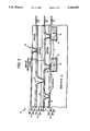
- a high density interconnect structure 10 in accordance with the present inventionis illustrated in a cross-section view in FIG. 3.
- the high density interconnect structure 10comprises a substrate 12 having cavities 14 in the upper surface thereof in which integrated circuit chips 16 or other electronic components are disposed. For many high density interconnect structures, these electronic components are bonded to the substrate with a thermoplastic adhesive 15. These electronic components have contact pads 18 on an (upper) contact surface thereof.
- the substrate 12may have conductive runs 13 disposed on the upper surface thereof.
- a first layer 20 of the overlying high density interconnect structure 10comprises a dielectric layer 22 and a patterned metallization layer 28.
- the dielectric layer 22has separate lower and upper sublayers 24 and 26, respectively.
- the upper sublayer 26may be a thermoset material or a high T g thermoplastic material.
- the layer 24is a thermoplastic adhesive having a first glass transition temperature T g1 .
- T g2glass transition temperature
- the upper sublayer 26 of the first dielectric layer 22should be stable over a range of temperatures above T g1 in order that it will remain stable during its lamination to the upper sublayer 26 be stable at least 100° C. above T g1 .
- stablewe mean it has sufficient viscosity that it doesn't shift, stretch or otherwise change in an undesirable manner during the lamination step.
- Upper sublayer 26is preferably a thermoset film, for example, Kapton® polyimide film which is sold by E. I. DuPont de Nemours. Other materials, including thermoplastics, which exhibit sufficient stability may also be used.
- the lower sublayer 24is preferably ULTEM® 1000 polyetherimide resin (T g1 ⁇ 217° C.) available from General Electric Company and the chip adhesive 15 is preferably ULTEM® 6000 polyetherimide resin (T g2 ⁇ 235° C.) available from General Electric Company.
- the patterned metallization layer 28extends into contact with contact pads 18 and conductor runs 13, if any, on the substrate 12 within via holes 23 in the dielectric layer 22.
- a second layer 30 of the high density interconnect structurecomprises a second dielectric layer 32 and a second patterned metallization layer 38.
- the dielectric layer 32comprises a thermoplastic release layer 34R and separate lower and upper sublayers 34 and 36, respectively.
- the release layermay preferably be SPI siloxane polyimide. This release layer is included in the structure to ensure its repairability in the event that one of the electronic components or the interconnection structure itself should turn out to be faulty. In the event that this structure must be disassembled for repair, it is heated to above T g1 so that the high density interconnect structure can be peeled off the substrate and electronic components.
- the second lower sublayer 34is a thermoset material and is preferably a copolymer blend of a polyimide and a crosslinkable epoxy of the type disclosed in U.S. patent application Ser. No. 454,545, entitled “An Epoxy/Polyimide Copolymer Blend Dielectric and Layered Circuits Incorporating It", which is listed above.
- the polyimide of this copolymer blendmay preferably be a siloxane polyimide which is fully reacted, such as siloxane polyimide SPI-129 or SPI-135 available from MicroSi.
- the crosslinkable epoxy of this copolymer blendmay preferably be a cycloaliphatic epoxy such as Ciba Geigy® CY179 (electronic grade) or Union Carbide® ERL 4221 (electronic grade). Other epoxies may also be used.
- This preferred compositionis considered particularly advantageous because these materials exhibit high radiation resistance with the result that they will survive x-ray and gamma ray environments which the silicon semiconductor chips interconnected by the high density interconnect structure will not survive. Further, the resulting structure is highly stable. We have exposed these materials to 200° C. for 4000 to 5000 hours with no visible change in their characteristics.
- the upper sublayer 36may again be a thermoset material or a thermoplastic material and is preferably a thermoset material (Kapton).
- the patterned metallization 38extends into via holes 33 in the dielectric layer 32 to make contact with the first metallization layer 28. If desired, selected via holes 33 may extend through dielectric layer 22 as well to provide direct contact to selected contact pads. However, that is not preferred because of the added processing complexity which results from having via holes of different depths and because of the adverse effect on repairability which results from having vias which connect directly to electronic component contact pads filled with a material which is still solid at temperatures in the 225° C. to 250° C. range.
- a third layer of the high density interconnect structure 40comprises a dielectric layer 42 and a patterned metallization layer 48.
- the dielectric layer 42has separate lower and upper sublayers 44 and 46.
- the third lower sublayer 44is preferably an SPI/epoxy crosslinking copolymer blend.
- the third upper dielectric sublayer 46may again be a thermoset material or a thermoplastic material and is preferably a thermoset. No release sublayer is needed under lower sublayer 44.
- the SPI/epoxy crosslinking copolymer blend adhesive materials 34 and 44are selected so that they become set at a low enough temperature that curing them has no adverse effect on the high density interconnect structure or the electronic components being connected thereby. This is in order that the structure may be fabricated and, if need be, disassembled without any adverse effect on the electronic components being interconnected, as taught in the background patents and applications.
- this inventioninvolves the use of SPI/epoxy crosslinking copolymer blend adhesives which adhere well both to the underlying metallization and dielectric layers, provide good adhesion for the film to be laminated thereover and have a stable B-stage at which the lamination can be performed and which cure at a low enough temperature to avoid adverse effects on the rest of the high density interconnect structure.
- These adhesive materialsare preferably inherently laser ablatable or should be rendered laser ablatable in accordance with U.S. patent application Ser. No. 456,421, entitled, "Laser Ablatable Polymer Dielectrics and Methods".
- That release layeris not required if the SPI/epoxy crosslinking copolymer blend has a low enough T g that the high density interconnect structure can be heated to a temperature at which the SPI/epoxy crosslinking copolymer blend itself is sufficiently fluid that divot removal is not a problem during removal of the high density interconnect structure for repair purposes.
- FIG. 4A preferred process 400 for producing the structure 10 shown in FIG. 3 is illustrated in FIG. 4.
- the process 400begins with Step 401 of mounting the chips on the substrate 12.
- This mountingmay be intended to be permanent where the substrate will remain part of the completed structure or may be intended to be temporary where the substrate will be removed following completion of the fabrication process in order to provide a flexible high density interconnect structure.
- This mountingis preferably done with ULTEM 6000 resin as the thermoplastic adhesive at a lamination temperature in the 250° C. to 300° C. range.
- the first upper sublayer 26 of dielectric materialis coated with an appropriate thermoplastic adhesive 24 which is preferably ULTEM® 1000 polyetherimide resin available from General Electric Company.
- this first dielectric layeris laminated to the chips and substrate at a first lamination temperature T 1 which for Ultem 1000 is typically in the 250° C. to 300° C. range.
- Step 404the via holes 23 are formed in this first dielectric layer.
- a patterned metallization layer 28is formed on this first dielectric layer. This may be done by forming a uniform metallization layer and then patterning it or by directly forming a patterned metallization layer as taught in the above-listed patents or by any of a variety of other patterned-deposition or uniform-deposition-followed-by-patterning techniques. This step completes the fabrication of the first layer 20 of the high density interconnect structure, as illustrated in FIG. 3.
- thermoplastic release sublayer 34Rwhich forms the first portion of the lower sublayer 34 is spun on on top of the first layer structure, that is, on top of the patterned metallization layer 28 and exposed portions of the first dielectric layer 22. This layer is then dried in a manner which is appropriate to that layer.
- Step 407a SPI/epoxy crosslinking copolymer blend is coated on top of the release layer as an adhesive.
- a copolymer blend of the polyimide and the crosslinkable epoxy source materials for this sublayeris formed to which a suitable curing agent for the epoxy is added, if needed. This material is then spin or spray coated on the release sublayer 34R in the process of forming the sublayer 34.
- a preferred source solutioncomprises a homogeneous blend of 200 grams of CY-179 cycloaliphatic epoxy resin from Ciba-Geigy and 472 grams of SPI-135 silicon polyimide polymer from MicroSi, 2.0 grams octyloxyphenyl (phenyl) iodonium hexafluoroantimonate catalyst from General Electric and 0.05 grams 12% copper naphthenate from Mooney Chemical.
- SPI-135consists of 175 grams of solids (37%) and 297 grams of diglyme/xylene solvent (63%).
- the solventis 80% diglyme and 20% xylene.
- Solventless depositionmay also be used as taught in U.S. patent application Ser. No. 454,545, entitled "An Epoxy/Polyimide Copolymer Blend Dielectric and Layered Circuits Incorporating It".
- this epoxy/polyimide copolymer blend layeris dried in Step 408 by heating the structure on a hot plate, or by other means, to a temperature T 2 of about 135° C. to drive off the solvent.
- T 2a temperature of about 135° C.
- this source solutionis spun on at 2600 rpm on a 2 ⁇ 2 inch substrate, approximately 70 milligrams of the solution is left evenly coated on the part. We then weigh the part every 30 minutes or so to determine the weight loss. We stop the drying process when the film has lost 47% of its weight.
- FIG. 5is a graph of the weight loss with time of a sample of this preferred source solution spun-on a substrate and dried in this manner. It will be observed that initially the solvent evaporates from the layer until the solvent is all gone. Then evaporation continues with the epoxy evaporating at the same time that it is curing. If this process is allowed to go to completion on a hot plate in this manner, then the final composition of the SPI/epoxy blend is about 63 wt % SPI and 37 wt % epoxy. We prefer to stop this drying process when about 10% of the epoxy has evaporated in order to be sure that all of the solvent is gone while still retaining most of the epoxy in the blend for a final composition of about 50:50 SPI:epoxy.
- the SPI/epoxy blendis no longer tacky and can be handled with ease and is generally about 12 ⁇ m thick. It is important to avoid curing this copolymer blend too far during this drying process, since that would result in poor adhesion between the laminated upper sublayer 36 and this adhesive lower sublayer 34 during lamination and would also result in void formation during the lamination process because the SPI/epoxy would not flow adequately during the lamination process to fill-in all depressions and other potential gaps between the Kapton upper sublayer film and this SPI/epoxy copolymer blend adhesive.
- Step 409we pretreat the underside of the upper (KAPTON) sublayer by reactive ion etching (RIE) in preparation for lamination to the SPI/epoxy blend adhesive in order to promote the creation of a strong bond between the SPI/epoxy blend and that upper sublayer.
- RIEreactive ion etching
- Step 410we place the part in the laminator at 80° C., apply vacuum to the top and bottom sides of the upper sublayer 36 to remove gases. After a sufficient evacuation time to obtain a base vacuum of 100 mTorr (typically about 20 minutes), a hydrostatic pressure of about 30-45 psi of nitrogen is applied to the upper surface of sublayer 36 to press the upper sublayer against the lower sublayer 34 and to cause sufficient flow of the SPI/epoxy blend to fill-in any potential voids. We then ramp the temperature up to a lamination temperature T 3 of 180° C. while maintaining pressure and hold the part at 180° C. for 30 minutes to finish the curing of the SPI/epoxy blend.
- T 3lamination temperature
- the curing timecan be reduced by increasing the curing temperature and that the curing temperature can be reduced if the curing time is increased.
- This curing/lamination temperature T 3 of 180° C.is comfortably below the T g of 217° C. of ULTEM 1000.
- the ULTEM 1000 adhesive sublayer 24remains rigid throughout this lamination process. This prevents the breaking of via connections as a result of the lamination pressure pushing the ULTEM 1000 thermoplastic resin layer back away from the vias as happened in the prior art samples in which vias broke during subsequent lamination at temperatures above the T g of the thermoplastic sublayer 24.
- the SPI/epoxy blendis preferably spun on at a slower speed to yield a thicker layer.
- the upper sublayer 36(Kapton) is preferably about 25 ⁇ m thick. Since this upper sublayer is preformed, its thickness is closely controlled. As a result, the dielectric layer 32 would have a thickness which is substantially 37 ⁇ m with a variation which is the variation in the thickness of the sublayer 34. However, this thickness is decreased by about 5 ⁇ m during the two RIE processing steps to which the Kapton layer is exposed.
- the first of theseis the adhesion promoting pretreatment with RIE which removes about 1 ⁇ m from the Kapton layer and the second is the post-via-drilling RIE clean-up etch designed to remove any ash or other remnants in the via holes following their drilling which removes about 4 ⁇ m.
- this processstill provides a much more uniform, much more repeatable thickness than a purely spun-on dielectric layer. This is highly desirable for use in microwave systems in which transmission lines are formed in the high density interconnect structure, since such dielectric layer uniformity and repeatability is important to being able to design and fabricate such transmission lines with the desired impedances.
- Step 411via holes are formed in this second dielectric layer.
- Step 412a second patterned metallization layer 38 is formed on top of the second dielectric layer 32 using the same or a different metallization technique as was used for the first metallization layer, as may be desired. This completes the fabrication of the second layer 30 of a high density interconnect structure of FIG. 3.
- Step 412coating the existing structure (that is, the patterned metallization layer 38 and exposed portions of the dielectric layer 32) with a SPI/epoxy crosslinking copolymer blend adhesive in accordance with the present invention.
- a SPI/epoxy crosslinking copolymer blend adhesivein accordance with the present invention.
- No thermoplastic release layeris needed here, although one can be provided if desired.
- this SPI/epoxy crosslinking copolymer blend adhesiveis dried at the temperature T 2 ( ⁇ 135° C.).
- Step 415the third upper dielectric sublayer 46 is pretreated and laminated to the top of the third SPI/epoxy crosslinking copolymer blend adhesive sublayer 44 at the lamination temperature T 3 ( ⁇ 180° C.).
- Step 416via holes 43 are formed in the third dielectric layer 42.
- Step 417a third patterned metallization layer 48 is formed on the third dielectric layer to complete the fabrication of the structure shown in FIG. 3. It will be recognized that additional layers of the high density interconnect structure may be fabricated in this same manner, if additional layers are needed or desired.
- An advantage of this multiple lamination structureis that it provides an ability to fabricate and pretest individual, basic high density interconnect structures of a complex system independently of each other. After such pretesting, the pretested, basic high density interconnect structures which make up the larger system are placed in their appropriate relative positions as shown generally at 300 in FIG. 6. These basic high density interconnect structures 318 are then interconnected by an overall high density interconnect structure 310 in the form of a further laminated dielectric layer 322 which bridges the gaps between adjacent basic high density interconnect structures 318. Metallization runs 328 which interconnect these various basic high density interconnect structures 318 through via holes 323 are then formed on the dielectric layer 322.
- the individual basic high density interconnect structures 318are preferably disposed in a carrier or substrate (not shown) during fabrication of the overall high density interconnect structure. That carrier or substrate may be retained in the final system as a support for the overall high density interconnect structure, including the basic high density interconnect structures 318. Alternatively, the carrier may be removed to leave the structure as shown.
- the overall high density interconnect structure 310is sufficiently flexible that the basic high density interconnect structures can be stacked by folding the portions of the overall high density interconnect structure which are disposed between the basic high density interconnect structures over on themselves.
- This ability to fabricate this overall high density interconnect structure by laminating its dielectric layer 322 to the basic high density interconnect structuresprovides a further increase in the versatility of high density interconnect structures over the structure shown in the drawings in application Ser. No. 07/504,769, entitled, "A Flexible High Density Interconnect Structure and Flexibly Interconnected System” in which the individual high density interconnect structure substrates are interconnected by the high density interconnect structure which interconnects the chips of the individual substrates.
- each of the adhesive layersshould to remain flexible throughout the life of the structure in order to facilitate repair of the structure in the event that one of the electronic components or a portion of the interconnect structure should be found to be faulty.
- Such flexibilityfacilitates peeling of the entire high density interconnect structure off the chips and substrate by heating above the T g1 of the thermoplastic sublayer 24 in the manner taught in U.S. Pat. No. 4,878,991, entitled "Simplified Method for Repair of High Density Interconnect Circuits", listed above and above the T g of the release sublayer 34R to prevent divot removal from contact pads.
- the structureis illustrated as including a substrate 12, it should be understood that in accordance with application Ser. No. 250,010, entitled, "High Density Interconnect With High Volumetric Efficiency” and application Ser. No. 07/504,769, entitled, "A Flexible High Density Interconnect Structure and Flexibly Interconnected System", the substrate may be removed following fabrication of the interconnect structure to leave the electronic components 16 bonded directly to the high density interconnect structure and otherwise unsupported.
- the existing structureAs has been described, it is preferred at each lamination step to coat the existing structure with the SPI/epoxy crosslinking copolymer blend lower sublayer of the next dielectric layer in order to facilitate planarization of that layer, especially in those situations where the a particularly thick metallization layer is used.
- the SPI/epoxy crosslinking copolymer blend adhesivemay be applied to the film of the upper sublayer instead. In that case, the adhesive layer should be thicker than the metallization runs it is to cover in order to avoid leaving voids in the structure adjacent those metallization runs.
- a final, upper, spun-on dielectric layermay be used, either for insulation purposes only or to support a final metallization layer. This avoids many of those problems with spun-on layers which arise only when two or more spun-on layers are used.
- a final laminated layermay be used which does not have via holes formed therein and does not have a metallization layer formed thereon. These same materials may also be used for the fabrication of printed circuit boards.
Landscapes
- Engineering & Computer Science (AREA)
- Computer Hardware Design (AREA)
- Microelectronics & Electronic Packaging (AREA)
- Power Engineering (AREA)
- Physics & Mathematics (AREA)
- Condensed Matter Physics & Semiconductors (AREA)
- General Physics & Mathematics (AREA)
- Ceramic Engineering (AREA)
- Manufacturing & Machinery (AREA)
- Production Of Multi-Layered Print Wiring Board (AREA)
- Manufacturing Of Printed Wiring (AREA)
Abstract
Description
Claims (19)
Priority Applications (4)
| Application Number | Priority Date | Filing Date | Title |
|---|---|---|---|
| US07/546,959US5161093A (en) | 1990-07-02 | 1990-07-02 | Multiple lamination high density interconnect process and structure employing a variable crosslinking adhesive |
| JP17331791AJP3246667B2 (en) | 1990-07-02 | 1991-06-19 | Multi-layer stacked high-density interconnect method and structure using variable crosslinkable adhesive |
| DE69128307TDE69128307T2 (en) | 1990-07-02 | 1991-07-01 | Process and structure for multilayer interconnection with high density |
| EP91305964AEP0465199B1 (en) | 1990-07-02 | 1991-07-01 | Multiple lamination high density interconnect process and structure |
Applications Claiming Priority (1)
| Application Number | Priority Date | Filing Date | Title |
|---|---|---|---|
| US07/546,959US5161093A (en) | 1990-07-02 | 1990-07-02 | Multiple lamination high density interconnect process and structure employing a variable crosslinking adhesive |
Publications (1)
| Publication Number | Publication Date |
|---|---|
| US5161093Atrue US5161093A (en) | 1992-11-03 |
Family
ID=24182728
Family Applications (1)
| Application Number | Title | Priority Date | Filing Date |
|---|---|---|---|
| US07/546,959Expired - LifetimeUS5161093A (en) | 1990-07-02 | 1990-07-02 | Multiple lamination high density interconnect process and structure employing a variable crosslinking adhesive |
Country Status (4)
| Country | Link |
|---|---|
| US (1) | US5161093A (en) |
| EP (1) | EP0465199B1 (en) |
| JP (1) | JP3246667B2 (en) |
| DE (1) | DE69128307T2 (en) |
Cited By (111)
| Publication number | Priority date | Publication date | Assignee | Title |
|---|---|---|---|---|
| US5285571A (en)* | 1992-10-13 | 1994-02-15 | General Electric Company | Method for extending an electrical conductor over an edge of an HDI substrate |
| US5353498A (en)* | 1993-02-08 | 1994-10-11 | General Electric Company | Method for fabricating an integrated circuit module |
| US5381445A (en)* | 1993-05-03 | 1995-01-10 | General Electric Company | Munitions cartridge transmitter |
| US5401687A (en)* | 1993-04-15 | 1995-03-28 | Martin Marietta Corporation | Process for high density interconnection of substrates and integrated circuit chips containing sensitive structures |
| US5432677A (en)* | 1993-02-09 | 1995-07-11 | Texas Instruments Incorporated | Multi-chip integrated circuit module |
| US5432675A (en)* | 1993-11-15 | 1995-07-11 | Fujitsu Limited | Multi-chip module having thermal contacts |
| US5434751A (en)* | 1994-04-11 | 1995-07-18 | Martin Marietta Corporation | Reworkable high density interconnect structure incorporating a release layer |
| US5472539A (en)* | 1994-06-06 | 1995-12-05 | General Electric Company | Methods for forming and positioning moldable permanent magnets on electromagnetically actuated microfabricated components |
| US5524339A (en)* | 1994-09-19 | 1996-06-11 | Martin Marietta Corporation | Method for protecting gallium arsenide mmic air bridge structures |
| EP0718885A2 (en) | 1994-12-19 | 1996-06-26 | Martin Marietta Corporation | Structure for protecting air bridges on semiconductor chips from damage |
| US5548099A (en)* | 1994-09-13 | 1996-08-20 | Martin Marietta Corporation | Method for making an electronics module having air bridge protection without large area ablation |
| US5552633A (en)* | 1995-06-06 | 1996-09-03 | Martin Marietta Corporation | Three-dimensional multimodule HDI arrays with heat spreading |
| US5626771A (en)* | 1994-06-02 | 1997-05-06 | International Business Machines Corporation | Design of high density structures with laser etch stop |
| EP0777274A1 (en) | 1995-11-30 | 1997-06-04 | Lockheed Martin Corporation | A high density interconnected circuit module with a compliant layer as part of a stress-reducing molded substrate |
| US5657537A (en)* | 1995-05-30 | 1997-08-19 | General Electric Company | Method for fabricating a stack of two dimensional circuit modules |
| WO1997042027A1 (en)* | 1996-05-06 | 1997-11-13 | Ameron International Corporation | Siloxane-modified adhesive/adherend systems |
| US5757623A (en)* | 1996-12-30 | 1998-05-26 | General Electric Company | Low-noise, high-Q stripline inductor |
| US5844810A (en)* | 1995-05-30 | 1998-12-01 | General Electric Company | Scaled adaptive lithography |
| US5874770A (en)* | 1996-10-10 | 1999-02-23 | General Electric Company | Flexible interconnect film including resistor and capacitor layers |
| US5888884A (en)* | 1998-01-02 | 1999-03-30 | General Electric Company | Electronic device pad relocation, precision placement, and packaging in arrays |
| US5888837A (en)* | 1996-04-16 | 1999-03-30 | General Electric Company | Chip burn-in and test structure and method |
| US5900674A (en)* | 1996-12-23 | 1999-05-04 | General Electric Company | Interface structures for electronic devices |
| US5904496A (en)* | 1997-01-24 | 1999-05-18 | Chipscale, Inc. | Wafer fabrication of inside-wrapped contacts for electronic devices |
| EP0849870A3 (en)* | 1996-12-17 | 1999-06-30 | General Electric Company | Matrix filters for low-noise power distribution systems |
| US5938452A (en)* | 1996-12-23 | 1999-08-17 | General Electric Company | Flexible interface structures for electronic devices |
| US6188301B1 (en) | 1998-11-13 | 2001-02-13 | General Electric Company | Switching structure and method of fabrication |
| US6188129B1 (en)* | 1997-03-24 | 2001-02-13 | Hyundai Electronics Industries Co., Ltd. | Stacked semiconductor chip package having external terminal pads and stackable chips having a protection layer |
| US6261467B1 (en)* | 1998-01-08 | 2001-07-17 | International Business Machines Corporation | Direct deposit thin film single/multi chip module |
| US6274391B1 (en)* | 1992-10-26 | 2001-08-14 | Texas Instruments Incorporated | HDI land grid array packaged device having electrical and optical interconnects |
| US6384483B1 (en)* | 1997-02-06 | 2002-05-07 | Nec Corporation | Manufacturing method for semiconductor device |
| US6400573B1 (en)* | 1993-02-09 | 2002-06-04 | Texas Instruments Incorporated | Multi-chip integrated circuit module |
| US20030062123A1 (en)* | 2001-09-28 | 2003-04-03 | Hrl Laboratories, Llc | Method of self-latching for adhesion during self-assembly of electronic or optical components |
| US20030068519A1 (en)* | 2001-09-28 | 2003-04-10 | Hrl Laboratories, Llc | Method for assembly of complementary-shaped receptacle site and device microstructures |
| US20030112576A1 (en)* | 2001-09-28 | 2003-06-19 | Brewer Peter D. | Process for producing high performance interconnects |
| US20030122244A1 (en)* | 2001-12-31 | 2003-07-03 | Mou-Shiung Lin | Integrated chip package structure using metal substrate and method of manufacturing the same |
| US20030140317A1 (en)* | 2001-09-28 | 2003-07-24 | Brewer Peter D. | Process for assembling three-dimensional systems on a chip and structure thus obtained |
| US20030178388A1 (en)* | 2002-03-22 | 2003-09-25 | Phillips Kenneth L. | Inverted micro-vias |
| US6680441B2 (en)* | 2001-06-13 | 2004-01-20 | Denso Corporation | Printed wiring board with embedded electric device and method for manufacturing printed wiring board with embedded electric device |
| US20040014317A1 (en)* | 2000-09-25 | 2004-01-22 | Hajime Sakamoto | Semiconductor element, method of manufacturing semiconductor element, multi-layer printed circuit board, and method of manufacturing multi-layer printed circuit board |
| WO2003030254A3 (en)* | 2001-09-28 | 2004-02-12 | Hrl Lab Llc | Process for assembling systems and structure thus obtained |
| US6693029B2 (en)* | 1999-10-12 | 2004-02-17 | Fujitsu Limited | Method of forming an insulative substrate having conductive filled vias |
| US20040061238A1 (en)* | 2002-09-30 | 2004-04-01 | Kabushiki Kaisha Toshiba | Semiconductor device and method of manufacturing the same |
| US20040088416A1 (en)* | 1997-11-25 | 2004-05-06 | Matsushita Electric Industrial Co., Ltd. | Printed circuit board and method manufacturing the same |
| US20040097078A1 (en)* | 2002-11-19 | 2004-05-20 | International Business Machines Corporation | Thin film transfer join process and multilevel thin film module |
| US6767764B2 (en) | 2001-03-15 | 2004-07-27 | General Electric Company | Microelectromechanical system device packaging method |
| US20040168825A1 (en)* | 2000-02-25 | 2004-09-02 | Hajime Sakamoto | Multilayer printed circuit board and multilayer printed circuit board manufacturing method |
| US20040203244A1 (en)* | 2002-02-13 | 2004-10-14 | Nobuo Oshima | Electronic component and fabricating method |
| US20040207068A1 (en)* | 2003-04-18 | 2004-10-21 | Leal George R. | Circuit device with at least partial packaging and method for forming |
| US6838750B2 (en)* | 2001-07-12 | 2005-01-04 | Custom One Design, Inc. | Interconnect circuitry, multichip module, and methods of manufacturing thereof |
| US6841740B2 (en)* | 2000-06-14 | 2005-01-11 | Ngk Spark Plug Co., Ltd. | Printed-wiring substrate and method for fabricating the same |
| US20050005424A1 (en)* | 2001-07-12 | 2005-01-13 | Custom One Design, Inc. | Method of manufacturing planar inductors |
| US6876554B1 (en)* | 1999-09-02 | 2005-04-05 | Ibiden Co., Ltd. | Printing wiring board and method of producing the same and capacitor to be contained in printed wiring board |
| US6921975B2 (en) | 2003-04-18 | 2005-07-26 | Freescale Semiconductor, Inc. | Circuit device with at least partial packaging, exposed active surface and a voltage reference plane |
| US20050163981A1 (en)* | 2004-01-28 | 2005-07-28 | Osthaus Bayard J. | Method for bonding ceramic to copper, without creating a bow in the copper |
| US20050242425A1 (en)* | 2004-04-30 | 2005-11-03 | Leal George R | Semiconductor device with a protected active die region and method therefor |
| US20050266557A1 (en)* | 2004-04-23 | 2005-12-01 | Hema-Quebec | Method of expanding cord blood cells |
| US20060027937A1 (en)* | 2004-08-06 | 2006-02-09 | Brad Benson | Electrical contact encapsulation |
| DE19842481B4 (en)* | 1997-11-19 | 2006-11-16 | LG Semicon Co., Ltd., Cheongju | Stackable semiconductor chip and method of manufacturing a stacked semiconductor chip module |
| US7223635B1 (en) | 2003-07-25 | 2007-05-29 | Hrl Laboratories, Llc | Oriented self-location of microstructures with alignment structures |
| US20070158811A1 (en)* | 2006-01-11 | 2007-07-12 | James Douglas Wehrly | Low profile managed memory component |
| US20070215997A1 (en)* | 2006-03-17 | 2007-09-20 | Martin Standing | Chip-scale package |
| US20070258225A1 (en)* | 1999-09-02 | 2007-11-08 | Ibiden, Co., Ltd. | Printed circuit board and method of manufacturing printed ciruit board |
| US20080148560A1 (en)* | 2006-12-20 | 2008-06-26 | Huankiat Seh | System and methods to laminate passives onto substrate |
| US20080314867A1 (en)* | 2007-06-21 | 2008-12-25 | General Electric Company | Method of making demountable interconnect structure |
| US20080318054A1 (en)* | 2007-06-21 | 2008-12-25 | General Electric Company | Low-temperature recoverable electronic component |
| US20080318413A1 (en)* | 2007-06-21 | 2008-12-25 | General Electric Company | Method for making an interconnect structure and interconnect component recovery process |
| US20080318055A1 (en)* | 2007-06-21 | 2008-12-25 | General Electric Company | Recoverable electronic component |
| US20080313894A1 (en)* | 2007-06-21 | 2008-12-25 | General Electric Company | Method for making an interconnect structure and low-temperature interconnect component recovery process |
| US20080318027A1 (en)* | 2007-06-21 | 2008-12-25 | General Electric Company | Demountable interconnect structure |
| US7485562B2 (en)* | 2002-08-27 | 2009-02-03 | Micron Technology, Inc. | Method of making multichip wafer level packages and computing systems incorporating same |
| EP2184774A1 (en)* | 2008-11-05 | 2010-05-12 | General Electric Company | Low-temperature recoverable electronic component |
| EP2184773A1 (en)* | 2008-11-05 | 2010-05-12 | General Electric Company | Recoverable electronic component |
| US20100148357A1 (en)* | 2008-12-16 | 2010-06-17 | Freescale Semiconductor, Inc. | Method of packaging integrated circuit dies with thermal dissipation capability |
| US7875952B1 (en) | 2006-09-19 | 2011-01-25 | Hrl Laboratories, Llc | Method of transistor level heterogeneous integration and system |
| US20110198762A1 (en)* | 2010-02-16 | 2011-08-18 | Deca Technologies Inc. | Panelized packaging with transferred dielectric |
| US20110209909A1 (en)* | 2011-05-05 | 2011-09-01 | Mixzon Incorporated | Noise dampening energy efficient circuit board and method for constructing and using same |
| US20110215450A1 (en)* | 2010-03-05 | 2011-09-08 | Chi Heejo | Integrated circuit packaging system with encapsulation and method of manufacture thereof |
| US20110225816A1 (en)* | 2010-03-16 | 2011-09-22 | Cheng-Hsien Chou | Method of manufacturing a multilayer printed circuit board with a built-in electronic device |
| US8310040B2 (en) | 2010-12-08 | 2012-11-13 | General Electric Company | Semiconductor device package having high breakdown voltage and low parasitic inductance and method of manufacturing thereof |
| US20120286422A1 (en)* | 2007-12-14 | 2012-11-15 | Stats Chippac, Ltd. | Semiconductor Device and Method of Forming Interconnect Structure for Encapsulated Die having Pre-Applied Protective Layer |
| US20130037929A1 (en)* | 2011-08-09 | 2013-02-14 | Kay S. Essig | Stackable wafer level packages and related methods |
| US8471361B2 (en) | 2001-12-31 | 2013-06-25 | Megica Corporation | Integrated chip package structure using organic substrate and method of manufacturing the same |
| US8492895B2 (en) | 2009-03-03 | 2013-07-23 | Panasonic Corporation | Semiconductor device with grounding conductor film formed on upper surface of dielectric film formed above integrated circuit |
| US8492870B2 (en) | 2002-01-19 | 2013-07-23 | Megica Corporation | Semiconductor package with interconnect layers |
| US8535976B2 (en) | 2001-12-31 | 2013-09-17 | Megica Corporation | Method for fabricating chip package with die and substrate |
| US20140035124A1 (en)* | 2012-08-02 | 2014-02-06 | Toyota Jidosha Kabushiki Kaisha | Semiconductor device and manufacturing method of same |
| US8786100B2 (en) | 2010-03-15 | 2014-07-22 | Stats Chippac, Ltd. | Semiconductor device and method of forming repassivation layer with reduced opening to contact pad of semiconductor die |
| TWI451827B (en)* | 2012-08-24 | 2014-09-01 | ||
| US8907476B2 (en) | 2010-03-12 | 2014-12-09 | Stats Chippac, Ltd. | Semiconductor device and method of forming sacrificial protective layer to protect semiconductor die edge during singulation |
| US8927339B2 (en) | 2010-11-22 | 2015-01-06 | Bridge Semiconductor Corporation | Method of making thermally enhanced semiconductor assembly with bump/base/flange heat spreader and build-up circuitry |
| US20150090688A1 (en)* | 2013-09-27 | 2015-04-02 | Avago Technologies General Ip (Singapore) Pte. Ltd | Method of fabricating printed circuit board (pcb) substrate having a cavity |
| US9030029B2 (en) | 2001-12-31 | 2015-05-12 | Qualcomm Incorporated | Chip package with die and substrate |
| US9087847B2 (en) | 2012-08-14 | 2015-07-21 | Bridge Semiconductor Corporation | Thermally enhanced interconnect substrate with embedded semiconductor device and built-in stopper and method of making the same |
| US20150380369A1 (en)* | 2013-09-30 | 2015-12-31 | Nantong Fujitsu Microelectronics Co., Ltd | Wafer packaging structure and packaging method |
| US20160044798A1 (en)* | 2013-06-18 | 2016-02-11 | Murata Manufacturing Co., Ltd. | Method of manufacturing resin multilayer substrate |
| WO2016025907A1 (en)* | 2014-08-15 | 2016-02-18 | Xamax Industries, Inc. | Composite thermoplastic laminate |
| US9318441B2 (en) | 2007-12-14 | 2016-04-19 | Stats Chippac, Ltd. | Semiconductor device and method of forming sacrificial adhesive over contact pads of semiconductor die |
| US9548240B2 (en) | 2010-03-15 | 2017-01-17 | STATS ChipPAC Pte. Ltd. | Semiconductor device and method of forming repassivation layer for robust low cost fan-out semiconductor package |
| US9666500B2 (en) | 2007-12-14 | 2017-05-30 | STATS ChipPAC Pte. Ltd. | Semiconductor device and method of forming insulating layer disposed over the semiconductor die for stress relief |
| US9754835B2 (en) | 2010-02-16 | 2017-09-05 | Deca Technologies Inc. | Semiconductor device and method comprising redistribution layers |
| US20180141321A1 (en)* | 2015-08-10 | 2018-05-24 | Murata Manufacturing Co., Ltd. | Resin multilayer substrate and method of manufacturing the same |
| US20190148289A1 (en)* | 2017-11-15 | 2019-05-16 | Samsung Electronics Co., Ltd. | Semiconductor device and method for fabricating the same |
| US10373870B2 (en) | 2010-02-16 | 2019-08-06 | Deca Technologies Inc. | Semiconductor device and method of packaging |
| TWI697996B (en)* | 2017-11-14 | 2020-07-01 | 台灣積體電路製造股份有限公司 | Semiconductor device and method of fabricating the same |
| US10882284B2 (en) | 2014-08-14 | 2021-01-05 | Mitsubishi Polyester Film, Inc. | Laminate containing coated polyester film |
| US20220109258A1 (en)* | 2020-10-02 | 2022-04-07 | Cellink Corporation | Forming connections to flexible interconnect circuits |
| US11562984B1 (en) | 2020-10-14 | 2023-01-24 | Hrl Laboratories, Llc | Integrated mechanical aids for high accuracy alignable-electrical contacts |
| US20230361048A1 (en)* | 2022-05-05 | 2023-11-09 | Taiwan Semiconductor Manufacturing Company, Ltd. | Semiconductor package and method of fabricating semiconductor package |
| US11876312B2 (en) | 2020-10-02 | 2024-01-16 | Cellink Corporation | Methods and systems for terminal-free circuit connectors and flexible multilayered interconnect circuits |
| US12057429B1 (en) | 2021-06-23 | 2024-08-06 | Hrl Laboratories, Llc | Temporary bonding structures for die-to-die and wafer-to-wafer bonding |
| US12444712B1 (en) | 2022-12-06 | 2025-10-14 | Hrl Laboratories, Llc | Integrated mechanical aids for high accuracy alignable-electrical contacts |
Families Citing this family (8)
| Publication number | Priority date | Publication date | Assignee | Title |
|---|---|---|---|---|
| US5300812A (en)* | 1992-12-09 | 1994-04-05 | General Electric Company | Plasticized polyetherimide adhesive composition and usage |
| US5397741A (en)* | 1993-03-29 | 1995-03-14 | International Business Machines Corporation | Process for metallized vias in polyimide |
| US6259148B1 (en) | 1998-08-13 | 2001-07-10 | International Business Machines Corporation | Modular high frequency integrated circuit structure |
| JP4931283B2 (en)* | 2000-09-25 | 2012-05-16 | イビデン株式会社 | Printed wiring board and printed wiring board manufacturing method |
| JP4771608B2 (en)* | 2000-12-15 | 2011-09-14 | イビデン株式会社 | Printed wiring board |
| JP4785268B2 (en)* | 2000-12-15 | 2011-10-05 | イビデン株式会社 | Multilayer printed wiring board with built-in semiconductor elements |
| US8076587B2 (en)* | 2008-09-26 | 2011-12-13 | Siemens Energy, Inc. | Printed circuit board for harsh environments |
| WO2021117191A1 (en)* | 2019-12-12 | 2021-06-17 | 太陽誘電株式会社 | Component module and production method for same |
Citations (8)
| Publication number | Priority date | Publication date | Assignee | Title |
|---|---|---|---|---|
| GB1171655A (en)* | 1966-02-26 | 1969-11-26 | Sony Kabushikikaisha Sony Corp | Method of Making Electrical Wiring and Wiring Circuit Connections between Conductors and the Electrodes of an Electrical Component |
| US4246595A (en)* | 1977-03-08 | 1981-01-20 | Matsushita Electric Industrial Co., Ltd. | Electronics circuit device and method of making the same |
| EP0222144A1 (en)* | 1985-10-05 | 1987-05-20 | Fujitsu Limited | A wafer-scale semiconductor device |
| US4783695A (en)* | 1986-09-26 | 1988-11-08 | General Electric Company | Multichip integrated circuit packaging configuration and method |
| EP0310010A2 (en)* | 1987-10-01 | 1989-04-05 | Mcgean-Rohco, Inc. | Multilayer printed circuit board formation |
| US4884122A (en)* | 1988-08-05 | 1989-11-28 | General Electric Company | Method and configuration for testing electronic circuits and integrated circuit chips using a removable overlay layer |
| US5073814A (en)* | 1990-07-02 | 1991-12-17 | General Electric Company | Multi-sublayer dielectric layers |
| US5108825A (en)* | 1989-12-21 | 1992-04-28 | General Electric Company | Epoxy/polyimide copolymer blend dielectric and layered circuits incorporating it |
- 1990
- 1990-07-02USUS07/546,959patent/US5161093A/ennot_activeExpired - Lifetime
- 1991
- 1991-06-19JPJP17331791Apatent/JP3246667B2/ennot_activeExpired - Lifetime
- 1991-07-01DEDE69128307Tpatent/DE69128307T2/ennot_activeExpired - Fee Related
- 1991-07-01EPEP91305964Apatent/EP0465199B1/ennot_activeExpired - Lifetime
Patent Citations (8)
| Publication number | Priority date | Publication date | Assignee | Title |
|---|---|---|---|---|
| GB1171655A (en)* | 1966-02-26 | 1969-11-26 | Sony Kabushikikaisha Sony Corp | Method of Making Electrical Wiring and Wiring Circuit Connections between Conductors and the Electrodes of an Electrical Component |
| US4246595A (en)* | 1977-03-08 | 1981-01-20 | Matsushita Electric Industrial Co., Ltd. | Electronics circuit device and method of making the same |
| EP0222144A1 (en)* | 1985-10-05 | 1987-05-20 | Fujitsu Limited | A wafer-scale semiconductor device |
| US4783695A (en)* | 1986-09-26 | 1988-11-08 | General Electric Company | Multichip integrated circuit packaging configuration and method |
| EP0310010A2 (en)* | 1987-10-01 | 1989-04-05 | Mcgean-Rohco, Inc. | Multilayer printed circuit board formation |
| US4884122A (en)* | 1988-08-05 | 1989-11-28 | General Electric Company | Method and configuration for testing electronic circuits and integrated circuit chips using a removable overlay layer |
| US5108825A (en)* | 1989-12-21 | 1992-04-28 | General Electric Company | Epoxy/polyimide copolymer blend dielectric and layered circuits incorporating it |
| US5073814A (en)* | 1990-07-02 | 1991-12-17 | General Electric Company | Multi-sublayer dielectric layers |
Cited By (245)
| Publication number | Priority date | Publication date | Assignee | Title |
|---|---|---|---|---|
| US5285571A (en)* | 1992-10-13 | 1994-02-15 | General Electric Company | Method for extending an electrical conductor over an edge of an HDI substrate |
| US6274391B1 (en)* | 1992-10-26 | 2001-08-14 | Texas Instruments Incorporated | HDI land grid array packaged device having electrical and optical interconnects |
| US5353498A (en)* | 1993-02-08 | 1994-10-11 | General Electric Company | Method for fabricating an integrated circuit module |
| US5497033A (en)* | 1993-02-08 | 1996-03-05 | Martin Marietta Corporation | Embedded substrate for integrated circuit modules |
| US5432677A (en)* | 1993-02-09 | 1995-07-11 | Texas Instruments Incorporated | Multi-chip integrated circuit module |
| US6400573B1 (en)* | 1993-02-09 | 2002-06-04 | Texas Instruments Incorporated | Multi-chip integrated circuit module |
| US5401687A (en)* | 1993-04-15 | 1995-03-28 | Martin Marietta Corporation | Process for high density interconnection of substrates and integrated circuit chips containing sensitive structures |
| US5381445A (en)* | 1993-05-03 | 1995-01-10 | General Electric Company | Munitions cartridge transmitter |
| US5432675A (en)* | 1993-11-15 | 1995-07-11 | Fujitsu Limited | Multi-chip module having thermal contacts |
| US5434751A (en)* | 1994-04-11 | 1995-07-18 | Martin Marietta Corporation | Reworkable high density interconnect structure incorporating a release layer |
| US5626771A (en)* | 1994-06-02 | 1997-05-06 | International Business Machines Corporation | Design of high density structures with laser etch stop |
| US5472539A (en)* | 1994-06-06 | 1995-12-05 | General Electric Company | Methods for forming and positioning moldable permanent magnets on electromagnetically actuated microfabricated components |
| US5548099A (en)* | 1994-09-13 | 1996-08-20 | Martin Marietta Corporation | Method for making an electronics module having air bridge protection without large area ablation |
| US5524339A (en)* | 1994-09-19 | 1996-06-11 | Martin Marietta Corporation | Method for protecting gallium arsenide mmic air bridge structures |
| US5561085A (en)* | 1994-12-19 | 1996-10-01 | Martin Marietta Corporation | Structure for protecting air bridges on semiconductor chips from damage |
| EP0718885A2 (en) | 1994-12-19 | 1996-06-26 | Martin Marietta Corporation | Structure for protecting air bridges on semiconductor chips from damage |
| US5844810A (en)* | 1995-05-30 | 1998-12-01 | General Electric Company | Scaled adaptive lithography |
| US5657537A (en)* | 1995-05-30 | 1997-08-19 | General Electric Company | Method for fabricating a stack of two dimensional circuit modules |
| US5552633A (en)* | 1995-06-06 | 1996-09-03 | Martin Marietta Corporation | Three-dimensional multimodule HDI arrays with heat spreading |
| US5866952A (en)* | 1995-11-30 | 1999-02-02 | Lockheed Martin Corporation | High density interconnected circuit module with a compliant layer as part of a stress-reducing molded substrate |
| EP0777274A1 (en) | 1995-11-30 | 1997-06-04 | Lockheed Martin Corporation | A high density interconnected circuit module with a compliant layer as part of a stress-reducing molded substrate |
| US5888837A (en)* | 1996-04-16 | 1999-03-30 | General Electric Company | Chip burn-in and test structure and method |
| US5946546A (en)* | 1996-04-16 | 1999-08-31 | General Electric Co. | Chip burn-in and test structure and method |
| WO1997042027A1 (en)* | 1996-05-06 | 1997-11-13 | Ameron International Corporation | Siloxane-modified adhesive/adherend systems |
| AU713161B2 (en)* | 1996-05-06 | 1999-11-25 | Ameron International Corporation | Siloxane-modified adhesive/adherend systems |
| US5874770A (en)* | 1996-10-10 | 1999-02-23 | General Electric Company | Flexible interconnect film including resistor and capacitor layers |
| US6323096B1 (en) | 1996-10-10 | 2001-11-27 | General Electric Company | Method for fabricating a flexible interconnect film with resistor and capacitor layers |
| EP0849870A3 (en)* | 1996-12-17 | 1999-06-30 | General Electric Company | Matrix filters for low-noise power distribution systems |
| US5938452A (en)* | 1996-12-23 | 1999-08-17 | General Electric Company | Flexible interface structures for electronic devices |
| US6298551B1 (en) | 1996-12-23 | 2001-10-09 | General Electric Company | Methods of forming compliant interface structures with partially open interiors for coupling two electrically conductive contact areas |
| US6046410A (en)* | 1996-12-23 | 2000-04-04 | General Electric Company | Interface structures for electronic devices |
| US5900674A (en)* | 1996-12-23 | 1999-05-04 | General Electric Company | Interface structures for electronic devices |
| US5757623A (en)* | 1996-12-30 | 1998-05-26 | General Electric Company | Low-noise, high-Q stripline inductor |
| US5904496A (en)* | 1997-01-24 | 1999-05-18 | Chipscale, Inc. | Wafer fabrication of inside-wrapped contacts for electronic devices |
| US6355981B1 (en) | 1997-01-24 | 2002-03-12 | Chipscale, Inc. | Wafer fabrication of inside-wrapped contacts for electronic devices |
| US6384483B1 (en)* | 1997-02-06 | 2002-05-07 | Nec Corporation | Manufacturing method for semiconductor device |
| US6188129B1 (en)* | 1997-03-24 | 2001-02-13 | Hyundai Electronics Industries Co., Ltd. | Stacked semiconductor chip package having external terminal pads and stackable chips having a protection layer |
| DE19842481B4 (en)* | 1997-11-19 | 2006-11-16 | LG Semicon Co., Ltd., Cheongju | Stackable semiconductor chip and method of manufacturing a stacked semiconductor chip module |
| US7068519B2 (en) | 1997-11-25 | 2006-06-27 | Matsushita Electric Industrial Co., Ltd. | Printed circuit board and method manufacturing the same |
| US20040088416A1 (en)* | 1997-11-25 | 2004-05-06 | Matsushita Electric Industrial Co., Ltd. | Printed circuit board and method manufacturing the same |
| US6002163A (en)* | 1998-01-02 | 1999-12-14 | General Electric Company | Electronic device pad relocation, precision placement, and packaging in arrays |
| US5888884A (en)* | 1998-01-02 | 1999-03-30 | General Electric Company | Electronic device pad relocation, precision placement, and packaging in arrays |
| US6261467B1 (en)* | 1998-01-08 | 2001-07-17 | International Business Machines Corporation | Direct deposit thin film single/multi chip module |
| US6655011B1 (en) | 1998-11-13 | 2003-12-02 | General Electric Company | Method for fabricating a switch structure |
| US6188301B1 (en) | 1998-11-13 | 2001-02-13 | General Electric Company | Switching structure and method of fabrication |
| US8763241B2 (en) | 1999-09-02 | 2014-07-01 | Ibiden Co., Ltd. | Method of manufacturing printed wiring board |
| US7978478B2 (en) | 1999-09-02 | 2011-07-12 | Ibiden Co., Ltd. | Printed circuit board |
| US7307852B2 (en) | 1999-09-02 | 2007-12-11 | Ibiden Co., Ltd. | Printed circuit board and method for manufacturing printed circuit board |
| US20070258225A1 (en)* | 1999-09-02 | 2007-11-08 | Ibiden, Co., Ltd. | Printed circuit board and method of manufacturing printed ciruit board |
| US20080055872A1 (en)* | 1999-09-02 | 2008-03-06 | Ibiden Co., Ltd. | Printed circuit board and method for manufacturing printed circuit board |
| US8331102B2 (en) | 1999-09-02 | 2012-12-11 | Ibiden Co., Ltd. | Printed circuit board |
| US20100118502A1 (en)* | 1999-09-02 | 2010-05-13 | Ibiden Co., Ltd. | Printed circuit board |
| US20080144298A1 (en)* | 1999-09-02 | 2008-06-19 | Ibiden, Co., Ltd. | Printed circuit board and method of manufacturing printed circuit board |
| US8780573B2 (en) | 1999-09-02 | 2014-07-15 | Ibiden Co., Ltd. | Printed circuit board |
| US8116091B2 (en) | 1999-09-02 | 2012-02-14 | Ibiden Co., Ltd. | Printed circuit board |
| US8107253B2 (en) | 1999-09-02 | 2012-01-31 | Ibiden Co., Ltd. | Printed circuit board |
| US20080142255A1 (en)* | 1999-09-02 | 2008-06-19 | Ibiden, Co., Ltd. | Printed circuit board and method of manufacturing printed circuit board |
| US20080158841A1 (en)* | 1999-09-02 | 2008-07-03 | Ibiden Co., Ltd. | Printed circuit board and method for manufacturing printed circuit board |
| US8717772B2 (en) | 1999-09-02 | 2014-05-06 | Ibiden Co., Ltd. | Printed circuit board |
| US7995352B2 (en) | 1999-09-02 | 2011-08-09 | Ibiden Co., Ltd. | Printed circuit board |
| US20100226108A1 (en)* | 1999-09-02 | 2010-09-09 | Ibiden, Co., Ltd. | Printed circuit board and method of manufacturing printed circuit board |
| US20080169120A1 (en)* | 1999-09-02 | 2008-07-17 | Ibiden, Co., Ltd. | Printed circuit board and method of manufacturing printed ciruit board |
| US9060446B2 (en) | 1999-09-02 | 2015-06-16 | Ibiden Co., Ltd. | Printed circuit board |
| US8842440B2 (en) | 1999-09-02 | 2014-09-23 | Ibiden Co., Ltd. | Printed circuit board and method of manufacturing printed circuit board |
| US8830691B2 (en) | 1999-09-02 | 2014-09-09 | Ibiden Co., Ltd. | Printed circuit board and method of manufacturing printed circuit board |
| US7881069B2 (en) | 1999-09-02 | 2011-02-01 | Ibiden Co., Ltd. | Printed circuit board |
| US6876554B1 (en)* | 1999-09-02 | 2005-04-05 | Ibiden Co., Ltd. | Printing wiring board and method of producing the same and capacitor to be contained in printed wiring board |
| US20100014261A1 (en)* | 1999-09-02 | 2010-01-21 | Ibiden Co., Ltd. | Printed circuit board and method of manufacturing printed circuit board |
| US7864542B2 (en) | 1999-09-02 | 2011-01-04 | Ibiden Co., Ltd. | Printed circuit board |
| US20050157478A1 (en)* | 1999-09-02 | 2005-07-21 | Ibiden Co., Ltd. | Printed circuit board and method for manufacturing printed circuit board |
| US7864543B2 (en) | 1999-09-02 | 2011-01-04 | Ibiden Co., Ltd. | Printed circuit board |
| US20100328915A1 (en)* | 1999-09-02 | 2010-12-30 | Ibiden Co., Ltd | Printed circuit board and method of manufacturing printed circuit board |
| US7855894B2 (en) | 1999-09-02 | 2010-12-21 | Ibiden Co., Ltd. | Printed circuit board |
| US6693029B2 (en)* | 1999-10-12 | 2004-02-17 | Fujitsu Limited | Method of forming an insulative substrate having conductive filled vias |
| US20040168825A1 (en)* | 2000-02-25 | 2004-09-02 | Hajime Sakamoto | Multilayer printed circuit board and multilayer printed circuit board manufacturing method |
| US20080201944A1 (en)* | 2000-02-25 | 2008-08-28 | Ibiden Co., Ltd. | Multilayer printed circuit board and multilayer printed circuit board manufacturing method |
| US20100018049A1 (en)* | 2000-02-25 | 2010-01-28 | Ibiden Co., Ltd. | Multilayer printed circuit board and multilayer printed circuit board manufacturing method |
| US6909054B2 (en)* | 2000-02-25 | 2005-06-21 | Ibiden Co., Ltd. | Multilayer printed wiring board and method for producing multilayer printed wiring board |
| US8453323B2 (en) | 2000-02-25 | 2013-06-04 | Ibiden Co., Ltd. | Printed circuit board manufacturing method |
| US7884286B2 (en) | 2000-02-25 | 2011-02-08 | Ibiden Co., Ltd. | Multilayer printed circuit board |
| US20090070996A1 (en)* | 2000-02-25 | 2009-03-19 | Ibiden Co., Ltd. | Printed circuit board manufacturing method |
| US7888605B2 (en) | 2000-02-25 | 2011-02-15 | Ibiden Co., Ltd. | Multilayer printed circuit board |
| US7435910B2 (en)* | 2000-02-25 | 2008-10-14 | Ibiden Co., Ltd. | Multilayer printed circuit board |
| US7842887B2 (en) | 2000-02-25 | 2010-11-30 | Ibiden Co., Ltd. | Multilayer printed circuit board |
| US7888606B2 (en) | 2000-02-25 | 2011-02-15 | Ibiden Co., Ltd. | Multilayer printed circuit board |
| US8046914B2 (en) | 2000-02-25 | 2011-11-01 | Ibiden Co., Ltd. | Method for manufacturing multilayer printed circuit board |
| US20080151520A1 (en)* | 2000-02-25 | 2008-06-26 | Ibiden Co., Ltd. | Multilayer printed circuit board and multilayer printed circuit board manufacturing method |
| US20080151517A1 (en)* | 2000-02-25 | 2008-06-26 | Ibiden Co., Ltd. | Multilayer printed circuit board and multilayer printed circuit board manufacturing method |
| US20080151519A1 (en)* | 2000-02-25 | 2008-06-26 | Ibiden Co., Ltd. | Multilayer printed circuit board and multilayer printed circuit board manufacturing method |
| US8079142B2 (en) | 2000-02-25 | 2011-12-20 | Ibiden Co., Ltd. | Printed circuit board manufacturing method |
| US8186045B2 (en)* | 2000-02-25 | 2012-05-29 | Ibiden Co., Ltd. | Multilayer printed circuit board and multilayer printed circuit board manufacturing method |
| US20070227765A1 (en)* | 2000-02-25 | 2007-10-04 | Ibiden Co., Ltd. | Multilayer printed circuit board and multilayer printed circuit board manufacturing method |
| US8438727B2 (en)* | 2000-02-25 | 2013-05-14 | Ibiden Co., Ltd. | Multilayer printed circuit board and multilayer printed circuit board manufacturing method |
| US6841740B2 (en)* | 2000-06-14 | 2005-01-11 | Ngk Spark Plug Co., Ltd. | Printed-wiring substrate and method for fabricating the same |
| US20090263939A1 (en)* | 2000-09-25 | 2009-10-22 | Ibiden Co., Ltd. | Semiconductor element, method of manufacturing semiconductor element, multi-layer printed circuit board, and method of manufacturing multi-layer printed circuit board |
| US20080230914A1 (en)* | 2000-09-25 | 2008-09-25 | Ibiden Co., Ltd. | Semiconductor element, method of manufacturing semiconductor element, multi-layer printed circuit board, and method of manufacturing multi-layer printed circuit board |
| US8959756B2 (en) | 2000-09-25 | 2015-02-24 | Ibiden Co., Ltd. | Method of manufacturing a printed circuit board having an embedded electronic component |
| US7999387B2 (en) | 2000-09-25 | 2011-08-16 | Ibiden Co., Ltd. | Semiconductor element connected to printed circuit board |
| US8067699B2 (en) | 2000-09-25 | 2011-11-29 | Ibiden Co., Ltd. | Semiconductor element, method of manufacturing semiconductor element, multi-layer printed circuit board, and method of manufacturing multi-layer printed circuit board |
| US7908745B2 (en) | 2000-09-25 | 2011-03-22 | Ibiden Co., Ltd. | Method of manufacturing multi-layer printed circuit board |
| US20070209831A1 (en)* | 2000-09-25 | 2007-09-13 | Ibiden Co., Ltd. | Semiconductor element, method of manufacturing semiconductor element, multi-layer printed circuit board, and method of manufacturing multi-layer printed circuit board |
| US7893360B2 (en) | 2000-09-25 | 2011-02-22 | Ibiden Co., Ltd. | Semiconductor element, method of manufacturing semiconductor element, multi-layer printed circuit board, and method of manufacturing multi-layer printed circuit board |
| US20040014317A1 (en)* | 2000-09-25 | 2004-01-22 | Hajime Sakamoto | Semiconductor element, method of manufacturing semiconductor element, multi-layer printed circuit board, and method of manufacturing multi-layer printed circuit board |
| US20080151522A1 (en)* | 2000-09-25 | 2008-06-26 | Ibiden Co., Ltd. | Semiconductor element, method of manufacturing semiconductor element, multi-layer printed circuit board, and method of manufacturing multi-layer printed circuit board |
| US20080148563A1 (en)* | 2000-09-25 | 2008-06-26 | Ibiden Co., Ltd. | Semiconductor element, method of manufacturing semiconductor element, multi-layer printed circuit board, and method of manufacturing multi-layer printed circuit board |
| US8822323B2 (en) | 2000-09-25 | 2014-09-02 | Ibiden Co., Ltd. | Semiconductor element, method of manufacturing semiconductor element, multi-layer printed circuit board, and method of manufacturing multi-layer printed circuit board |
| US7855342B2 (en) | 2000-09-25 | 2010-12-21 | Ibiden Co., Ltd. | Semiconductor element, method of manufacturing semiconductor element, multi-layer printed circuit board, and method of manufacturing multi-layer printed circuit board |
| US7852634B2 (en) | 2000-09-25 | 2010-12-14 | Ibiden Co., Ltd. | Semiconductor element, method of manufacturing semiconductor element, multi-layer printed circuit board, and method of manufacturing multi-layer printed circuit board |
| US8293579B2 (en) | 2000-09-25 | 2012-10-23 | Ibiden Co., Ltd. | Semiconductor element, method of manufacturing semiconductor element, multi-layer printed circuit board, and method of manufacturing multi-layer printed circuit board |
| US9245838B2 (en) | 2000-09-25 | 2016-01-26 | Ibiden Co., Ltd. | Semiconductor element |
| US8524535B2 (en) | 2000-09-25 | 2013-09-03 | Ibiden Co., Ltd. | Semiconductor element, method of manufacturing semiconductor element, multi-layer printed circuit board, and method of manufacturing multi-layer printed circuit board |
| US20100140803A1 (en)* | 2000-09-25 | 2010-06-10 | Ibiden Co., Ltd. | Semiconductor element, method of manufacturing semiconductor element, multi-layer printed circuit board, and method of manufacturing multi-layer printed circuit board |
| US6773962B2 (en) | 2001-03-15 | 2004-08-10 | General Electric Company | Microelectromechanical system device packaging method |
| US6767764B2 (en) | 2001-03-15 | 2004-07-27 | General Electric Company | Microelectromechanical system device packaging method |
| US7165321B2 (en) | 2001-06-13 | 2007-01-23 | Denso Corporation | Method for manufacturing printed wiring board with embedded electric device |
| US6680441B2 (en)* | 2001-06-13 | 2004-01-20 | Denso Corporation | Printed wiring board with embedded electric device and method for manufacturing printed wiring board with embedded electric device |
| US20040091687A1 (en)* | 2001-06-13 | 2004-05-13 | Koji Kondo | Method for manufacturing printed wiring board with embedded electric device |
| US20050153061A1 (en)* | 2001-07-12 | 2005-07-14 | Custom One Design, Inc. | Interconnect circuitry, multichip module, and methods for making them |
| US7449412B2 (en) | 2001-07-12 | 2008-11-11 | Custom One Design, Inc. | Interconnect circuitry, multichip module, and methods of manufacturing thereof |
| US6838750B2 (en)* | 2001-07-12 | 2005-01-04 | Custom One Design, Inc. | Interconnect circuitry, multichip module, and methods of manufacturing thereof |
| US20050005424A1 (en)* | 2001-07-12 | 2005-01-13 | Custom One Design, Inc. | Method of manufacturing planar inductors |
| US20070155176A1 (en)* | 2001-07-12 | 2007-07-05 | Custom One Design, Inc. | Interconnect circuitry, multichip module, and methods of manufacturing thereof |
| US7231707B2 (en) | 2001-07-12 | 2007-06-19 | Custom One Design, Inc. | Method of manufacturing planar inductors |
| US7179742B2 (en) | 2001-07-12 | 2007-02-20 | Custom One Design, Inc. | Interconnect circuitry, multichip module, and methods for making them |
| US20030068519A1 (en)* | 2001-09-28 | 2003-04-10 | Hrl Laboratories, Llc | Method for assembly of complementary-shaped receptacle site and device microstructures |
| WO2003030254A3 (en)* | 2001-09-28 | 2004-02-12 | Hrl Lab Llc | Process for assembling systems and structure thus obtained |
| US7351660B2 (en) | 2001-09-28 | 2008-04-01 | Hrl Laboratories, Llc | Process for producing high performance interconnects |
| US20030062123A1 (en)* | 2001-09-28 | 2003-04-03 | Hrl Laboratories, Llc | Method of self-latching for adhesion during self-assembly of electronic or optical components |
| US20030140317A1 (en)* | 2001-09-28 | 2003-07-24 | Brewer Peter D. | Process for assembling three-dimensional systems on a chip and structure thus obtained |
| US6974604B2 (en) | 2001-09-28 | 2005-12-13 | Hrl Laboratories, Llc | Method of self-latching for adhesion during self-assembly of electronic or optical components |
| US7253091B2 (en) | 2001-09-28 | 2007-08-07 | Hrl Laboratories, Llc | Process for assembling three-dimensional systems on a chip and structure thus obtained |
| US7018575B2 (en) | 2001-09-28 | 2006-03-28 | Hrl Laboratories, Llc | Method for assembly of complementary-shaped receptacle site and device microstructures |
| US20030112576A1 (en)* | 2001-09-28 | 2003-06-19 | Brewer Peter D. | Process for producing high performance interconnects |
| US20030122244A1 (en)* | 2001-12-31 | 2003-07-03 | Mou-Shiung Lin | Integrated chip package structure using metal substrate and method of manufacturing the same |
| US8471361B2 (en) | 2001-12-31 | 2013-06-25 | Megica Corporation | Integrated chip package structure using organic substrate and method of manufacturing the same |
| US8835221B2 (en) | 2001-12-31 | 2014-09-16 | Qualcomm Incorporated | Integrated chip package structure using ceramic substrate and method of manufacturing the same |
| US8119446B2 (en)* | 2001-12-31 | 2012-02-21 | Megica Corporation | Integrated chip package structure using metal substrate and method of manufacturing the same |
| US9030029B2 (en) | 2001-12-31 | 2015-05-12 | Qualcomm Incorporated | Chip package with die and substrate |
| US8535976B2 (en) | 2001-12-31 | 2013-09-17 | Megica Corporation | Method for fabricating chip package with die and substrate |
| US9136246B2 (en) | 2001-12-31 | 2015-09-15 | Qualcomm Incorporated | Integrated chip package structure using silicon substrate and method of manufacturing the same |
| US8492870B2 (en) | 2002-01-19 | 2013-07-23 | Megica Corporation | Semiconductor package with interconnect layers |
| US20040203244A1 (en)* | 2002-02-13 | 2004-10-14 | Nobuo Oshima | Electronic component and fabricating method |
| US20030178388A1 (en)* | 2002-03-22 | 2003-09-25 | Phillips Kenneth L. | Inverted micro-vias |
| US7485562B2 (en)* | 2002-08-27 | 2009-02-03 | Micron Technology, Inc. | Method of making multichip wafer level packages and computing systems incorporating same |
| US20040061238A1 (en)* | 2002-09-30 | 2004-04-01 | Kabushiki Kaisha Toshiba | Semiconductor device and method of manufacturing the same |
| US6831367B2 (en)* | 2002-09-30 | 2004-12-14 | Kabushiki Kaisha Toshiba | Semiconductor device and method of manufacturing the same |
| US6998327B2 (en) | 2002-11-19 | 2006-02-14 | International Business Machines Corporation | Thin film transfer join process and multilevel thin film module |
| US20040097078A1 (en)* | 2002-11-19 | 2004-05-20 | International Business Machines Corporation | Thin film transfer join process and multilevel thin film module |
| US8072062B2 (en) | 2003-04-18 | 2011-12-06 | Freescale Semiconductor, Inc. | Circuit device with at least partial packaging and method for forming |
| US20040207068A1 (en)* | 2003-04-18 | 2004-10-21 | Leal George R. | Circuit device with at least partial packaging and method for forming |
| US20080142960A1 (en)* | 2003-04-18 | 2008-06-19 | Freescale Semiconductor, Inc. | Circuit device with at least partial packaging and method for forming |
| US7361987B2 (en) | 2003-04-18 | 2008-04-22 | Freescale Semiconductor, Inc. | Circuit device with at least partial packaging and method for forming |
| US6838776B2 (en) | 2003-04-18 | 2005-01-04 | Freescale Semiconductor, Inc. | Circuit device with at least partial packaging and method for forming |
| US6921975B2 (en) | 2003-04-18 | 2005-07-26 | Freescale Semiconductor, Inc. | Circuit device with at least partial packaging, exposed active surface and a voltage reference plane |
| US7622813B2 (en) | 2003-07-25 | 2009-11-24 | Hrl Laboratories, Llc | Oriented self-location of microstructures with alignment structures |
| US7223635B1 (en) | 2003-07-25 | 2007-05-29 | Hrl Laboratories, Llc | Oriented self-location of microstructures with alignment structures |
| US20070252289A1 (en)* | 2003-07-25 | 2007-11-01 | Hrl Laboratories, Llc | Oriented self-location of microstructures with alignment structures |
| US6933443B2 (en)* | 2004-01-28 | 2005-08-23 | Infineon Technologies North America Corp. | Method for bonding ceramic to copper, without creating a bow in the copper |
| US20050163981A1 (en)* | 2004-01-28 | 2005-07-28 | Osthaus Bayard J. | Method for bonding ceramic to copper, without creating a bow in the copper |
| US20050266557A1 (en)* | 2004-04-23 | 2005-12-01 | Hema-Quebec | Method of expanding cord blood cells |
| US7579219B2 (en) | 2004-04-30 | 2009-08-25 | Freescale Semiconductor, Inc. | Semiconductor device with a protected active die region and method therefor |
| US20050242425A1 (en)* | 2004-04-30 | 2005-11-03 | Leal George R | Semiconductor device with a protected active die region and method therefor |
| US20060192301A1 (en)* | 2004-04-30 | 2006-08-31 | Leal George R | Semiconductor device with a protected active die region and method therefor |
| US7475964B2 (en) | 2004-08-06 | 2009-01-13 | Hewlett-Packard Development Company, L.P. | Electrical contact encapsulation |
| US20060027937A1 (en)* | 2004-08-06 | 2006-02-09 | Brad Benson | Electrical contact encapsulation |
| US20070158811A1 (en)* | 2006-01-11 | 2007-07-12 | James Douglas Wehrly | Low profile managed memory component |
| US20070215997A1 (en)* | 2006-03-17 | 2007-09-20 | Martin Standing | Chip-scale package |
| US7875952B1 (en) | 2006-09-19 | 2011-01-25 | Hrl Laboratories, Llc | Method of transistor level heterogeneous integration and system |
| US7838419B2 (en)* | 2006-12-20 | 2010-11-23 | Intel Corporation | Systems and methods to laminate passives onto substrate |
| US7981758B2 (en) | 2006-12-20 | 2011-07-19 | Intel Corporation | Systems and methods to laminate passives onto substrate |
| US20080148560A1 (en)* | 2006-12-20 | 2008-06-26 | Huankiat Seh | System and methods to laminate passives onto substrate |
| US20110034002A1 (en)* | 2006-12-20 | 2011-02-10 | Huankiat Seh | Systems and methods to laminate passives onto substrate |
| US9953910B2 (en) | 2007-06-21 | 2018-04-24 | General Electric Company | Demountable interconnect structure |
| US9610758B2 (en) | 2007-06-21 | 2017-04-04 | General Electric Company | Method of making demountable interconnect structure |
| US20080318027A1 (en)* | 2007-06-21 | 2008-12-25 | General Electric Company | Demountable interconnect structure |
| US20080313894A1 (en)* | 2007-06-21 | 2008-12-25 | General Electric Company | Method for making an interconnect structure and low-temperature interconnect component recovery process |
| US20080318055A1 (en)* | 2007-06-21 | 2008-12-25 | General Electric Company | Recoverable electronic component |
| US20080318413A1 (en)* | 2007-06-21 | 2008-12-25 | General Electric Company | Method for making an interconnect structure and interconnect component recovery process |
| US20080318054A1 (en)* | 2007-06-21 | 2008-12-25 | General Electric Company | Low-temperature recoverable electronic component |
| US20080314867A1 (en)* | 2007-06-21 | 2008-12-25 | General Electric Company | Method of making demountable interconnect structure |
| US20120286422A1 (en)* | 2007-12-14 | 2012-11-15 | Stats Chippac, Ltd. | Semiconductor Device and Method of Forming Interconnect Structure for Encapsulated Die having Pre-Applied Protective Layer |
| US9559029B2 (en) | 2007-12-14 | 2017-01-31 | STATS ChipPAC Pte. Ltd. | Semiconductor device and method of forming interconnect structure for encapsulated die having pre-applied protective layer |
| US10998248B2 (en) | 2007-12-14 | 2021-05-04 | JCET Semiconductor (Shaoxing) Co. Ltd. | Semiconductor device and method of forming sacrificial adhesive over contact pads of semiconductor die |
| US9252066B2 (en) | 2007-12-14 | 2016-02-02 | Stats Chippac, Ltd. | Semiconductor device and method of forming interconnect structure for encapsulated die having pre-applied protective layer |
| US9666500B2 (en) | 2007-12-14 | 2017-05-30 | STATS ChipPAC Pte. Ltd. | Semiconductor device and method of forming insulating layer disposed over the semiconductor die for stress relief |
| US9318441B2 (en) | 2007-12-14 | 2016-04-19 | Stats Chippac, Ltd. | Semiconductor device and method of forming sacrificial adhesive over contact pads of semiconductor die |
| US8846454B2 (en)* | 2007-12-14 | 2014-09-30 | Stats Chippac, Ltd. | Semiconductor device and method of forming interconnect structure for encapsulated die having pre-applied protective layer |
| EP2184773A1 (en)* | 2008-11-05 | 2010-05-12 | General Electric Company | Recoverable electronic component |
| EP2184774A1 (en)* | 2008-11-05 | 2010-05-12 | General Electric Company | Low-temperature recoverable electronic component |
| US20100148357A1 (en)* | 2008-12-16 | 2010-06-17 | Freescale Semiconductor, Inc. | Method of packaging integrated circuit dies with thermal dissipation capability |
| US8492895B2 (en) | 2009-03-03 | 2013-07-23 | Panasonic Corporation | Semiconductor device with grounding conductor film formed on upper surface of dielectric film formed above integrated circuit |
| US10373870B2 (en) | 2010-02-16 | 2019-08-06 | Deca Technologies Inc. | Semiconductor device and method of packaging |
| US20110198762A1 (en)* | 2010-02-16 | 2011-08-18 | Deca Technologies Inc. | Panelized packaging with transferred dielectric |
| US20140225271A1 (en)* | 2010-02-16 | 2014-08-14 | Deca Technologies Inc. | Panelized packaging with transferred dielectric |
| US9754835B2 (en) | 2010-02-16 | 2017-09-05 | Deca Technologies Inc. | Semiconductor device and method comprising redistribution layers |
| US20110215450A1 (en)* | 2010-03-05 | 2011-09-08 | Chi Heejo | Integrated circuit packaging system with encapsulation and method of manufacture thereof |
| US10204866B2 (en) | 2010-03-12 | 2019-02-12 | STATS ChipPAC Pte. Ltd. | Semiconductor device and method of forming sacrificial protective layer to protect semiconductor die edge during singulation |
| US8907476B2 (en) | 2010-03-12 | 2014-12-09 | Stats Chippac, Ltd. | Semiconductor device and method of forming sacrificial protective layer to protect semiconductor die edge during singulation |
| US9558958B2 (en) | 2010-03-12 | 2017-01-31 | STATS ChipPAC Pte. Ltd. | Semiconductor device and method of forming sacrificial protective layer to protect semiconductor die edge during singulation |
| US9754867B2 (en) | 2010-03-15 | 2017-09-05 | STATS ChipPAC Pte. Ltd. | Semiconductor device and method of forming repassivation layer for robust low cost fan-out semiconductor package |
| US8786100B2 (en) | 2010-03-15 | 2014-07-22 | Stats Chippac, Ltd. | Semiconductor device and method of forming repassivation layer with reduced opening to contact pad of semiconductor die |
| US9548240B2 (en) | 2010-03-15 | 2017-01-17 | STATS ChipPAC Pte. Ltd. | Semiconductor device and method of forming repassivation layer for robust low cost fan-out semiconductor package |
| US9472452B2 (en) | 2010-03-15 | 2016-10-18 | STATS ChipPAC Pte. Ltd. | Semiconductor device and method of forming repassivation layer with reduced opening to contact pad of semiconductor die |
| US20110225816A1 (en)* | 2010-03-16 | 2011-09-22 | Cheng-Hsien Chou | Method of manufacturing a multilayer printed circuit board with a built-in electronic device |
| US8302299B2 (en)* | 2010-03-16 | 2012-11-06 | Unitech Printed Circuit Board Corp. | Method of manufacturing a multilayer printed circuit board with a built-in electronic device |
| US8927339B2 (en) | 2010-11-22 | 2015-01-06 | Bridge Semiconductor Corporation | Method of making thermally enhanced semiconductor assembly with bump/base/flange heat spreader and build-up circuitry |
| US8310040B2 (en) | 2010-12-08 | 2012-11-13 | General Electric Company | Semiconductor device package having high breakdown voltage and low parasitic inductance and method of manufacturing thereof |
| US8586421B2 (en) | 2010-12-08 | 2013-11-19 | General Electric Company | Method of forming semiconductor device package having high breakdown voltage and low parasitic inductance |
| US20110209909A1 (en)* | 2011-05-05 | 2011-09-01 | Mixzon Incorporated | Noise dampening energy efficient circuit board and method for constructing and using same |
| US8569631B2 (en) | 2011-05-05 | 2013-10-29 | Tangitek, Llc | Noise dampening energy efficient circuit board and method for constructing and using same |
| US20130037929A1 (en)* | 2011-08-09 | 2013-02-14 | Kay S. Essig | Stackable wafer level packages and related methods |
| US20140035124A1 (en)* | 2012-08-02 | 2014-02-06 | Toyota Jidosha Kabushiki Kaisha | Semiconductor device and manufacturing method of same |
| US9082778B2 (en)* | 2012-08-02 | 2015-07-14 | Toyota Jidosha Kabushiki Kaisha | Semiconductor device and manufacturing method of same |
| CN103579303B (en)* | 2012-08-02 | 2017-06-06 | 丰田自动车株式会社 | Semiconductor device and its manufacture method |
| CN103579303A (en)* | 2012-08-02 | 2014-02-12 | 丰田自动车株式会社 | Semiconductor device and manufacturing method of same |
| US9087847B2 (en) | 2012-08-14 | 2015-07-21 | Bridge Semiconductor Corporation | Thermally enhanced interconnect substrate with embedded semiconductor device and built-in stopper and method of making the same |
| TWI451827B (en)* | 2012-08-24 | 2014-09-01 | ||
| US20160044798A1 (en)* | 2013-06-18 | 2016-02-11 | Murata Manufacturing Co., Ltd. | Method of manufacturing resin multilayer substrate |
| US10098238B2 (en)* | 2013-06-18 | 2018-10-09 | Murata Manufacturing Co., Ltd. | Method of manufacturing resin multilayer substrate |
| US9085826B2 (en)* | 2013-09-27 | 2015-07-21 | Avago Technologies General Ip (Singapore) Pte. Ltd. | Method of fabricating printed circuit board (PCB) substrate having a cavity |
| US20150090688A1 (en)* | 2013-09-27 | 2015-04-02 | Avago Technologies General Ip (Singapore) Pte. Ltd | Method of fabricating printed circuit board (pcb) substrate having a cavity |
| US20150380369A1 (en)* | 2013-09-30 | 2015-12-31 | Nantong Fujitsu Microelectronics Co., Ltd | Wafer packaging structure and packaging method |
| US11725089B2 (en) | 2014-08-14 | 2023-08-15 | Mitsubishi Chemical America, Inc. | Laminate containing coated polyester film |
| US10882284B2 (en) | 2014-08-14 | 2021-01-05 | Mitsubishi Polyester Film, Inc. | Laminate containing coated polyester film |
| US10730277B2 (en) | 2014-08-15 | 2020-08-04 | Xamax Industries, Inc. | Composite thermoplastic laminate |
| WO2016025907A1 (en)* | 2014-08-15 | 2016-02-18 | Xamax Industries, Inc. | Composite thermoplastic laminate |
| US10350867B2 (en) | 2014-08-15 | 2019-07-16 | Xamax Industries, Inc. | Composite thermoplastic laminate |
| US9636893B2 (en) | 2014-08-15 | 2017-05-02 | Xamax Industries, Inc. | Composite thermoplastic laminate |
| US20180141321A1 (en)* | 2015-08-10 | 2018-05-24 | Murata Manufacturing Co., Ltd. | Resin multilayer substrate and method of manufacturing the same |
| US10166747B2 (en)* | 2015-08-10 | 2019-01-01 | Murata Manufacturing Co., Ltd. | Resin multilayer substrate and method of manufacturing the same |
| TWI697996B (en)* | 2017-11-14 | 2020-07-01 | 台灣積體電路製造股份有限公司 | Semiconductor device and method of fabricating the same |
| US10727178B2 (en) | 2017-11-14 | 2020-07-28 | Taiwan Semiconductor Manufacturing Co., Ltd. | Via structure and methods thereof |
| US10854542B2 (en) | 2017-11-14 | 2020-12-01 | Taiwan Semiconductor Manufacturing Co., Ltd. | Via structure and methods thereof |
| US11854962B2 (en) | 2017-11-14 | 2023-12-26 | Taiwan Semiconductor Manufacturing Co., Ltd. | Via structure and methods thereof |
| US20190148289A1 (en)* | 2017-11-15 | 2019-05-16 | Samsung Electronics Co., Ltd. | Semiconductor device and method for fabricating the same |
| US10535600B2 (en)* | 2017-11-15 | 2020-01-14 | Samsung Electronics Co., Ltd. | Semiconductor device |
| US20220109258A1 (en)* | 2020-10-02 | 2022-04-07 | Cellink Corporation | Forming connections to flexible interconnect circuits |
| US11791577B2 (en)* | 2020-10-02 | 2023-10-17 | Cellink Corporation | Forming connections to flexible interconnect circuits |
| US20230402776A1 (en)* | 2020-10-02 | 2023-12-14 | Cellink Corporation | Forming connections to flexible interconnect circuits |
| US11876312B2 (en) | 2020-10-02 | 2024-01-16 | Cellink Corporation | Methods and systems for terminal-free circuit connectors and flexible multilayered interconnect circuits |
| US12176640B2 (en)* | 2020-10-02 | 2024-12-24 | Cellink Corporation | Forming connections to flexible interconnect circuits |
| US11562984B1 (en) | 2020-10-14 | 2023-01-24 | Hrl Laboratories, Llc | Integrated mechanical aids for high accuracy alignable-electrical contacts |
| US12057429B1 (en) | 2021-06-23 | 2024-08-06 | Hrl Laboratories, Llc | Temporary bonding structures for die-to-die and wafer-to-wafer bonding |
| US20230361048A1 (en)* | 2022-05-05 | 2023-11-09 | Taiwan Semiconductor Manufacturing Company, Ltd. | Semiconductor package and method of fabricating semiconductor package |
| US12444712B1 (en) | 2022-12-06 | 2025-10-14 | Hrl Laboratories, Llc | Integrated mechanical aids for high accuracy alignable-electrical contacts |
Also Published As
| Publication number | Publication date |
|---|---|
| EP0465199B1 (en) | 1997-12-03 |
| DE69128307T2 (en) | 1998-06-25 |
| JP3246667B2 (en) | 2002-01-15 |
| JPH04233265A (en) | 1992-08-21 |
| EP0465199A1 (en) | 1992-01-08 |
| DE69128307D1 (en) | 1998-01-15 |
Similar Documents
| Publication | Publication Date | Title |
|---|---|---|
| US5161093A (en) | Multiple lamination high density interconnect process and structure employing a variable crosslinking adhesive | |
| US5157589A (en) | Mutliple lamination high density interconnect process and structure employing thermoplastic adhesives having sequentially decreasing TG 's | |
| US5108825A (en) | Epoxy/polyimide copolymer blend dielectric and layered circuits incorporating it | |
| US5745984A (en) | Method for making an electronic module | |
| US5073814A (en) | Multi-sublayer dielectric layers | |
| US5434751A (en) | Reworkable high density interconnect structure incorporating a release layer | |
| US5232548A (en) | Discrete fabrication of multi-layer thin film, wiring structures | |
| JP3802936B2 (en) | Integrated circuit module | |
| EP0130417B1 (en) | A method of fabricating an electrical interconnection structure for an integrated circuit module | |
| US5866952A (en) | High density interconnected circuit module with a compliant layer as part of a stress-reducing molded substrate | |
| US5548099A (en) | Method for making an electronics module having air bridge protection without large area ablation | |
| US6939738B2 (en) | Component built-in module and method for producing the same | |
| EP0987760B1 (en) | Multichip-module fabrication process | |
| US4918811A (en) | Multichip integrated circuit packaging method | |
| JP3641002B2 (en) | Sealed integrally molded plastic multichip module substrate and manufacturing method | |
| WO1988002552A1 (en) | Multichip integrated circuit packaging configuration and method | |
| JPH08236628A (en) | Structure for protecting air bridge on semiconductor chip from damage | |
| US20040089470A1 (en) | Printed circuit board, semiconductor package, base insulating film, and manufacturing method for interconnect substrate | |
| US6256874B1 (en) | Conductor interconnect with dendrites through film and method for producing same | |
| EP0434311B1 (en) | An epoxy/polyimide copolymer blend dielectric in multilayered circuits | |
| CA2049272C (en) | Multiple lamination high density interconnect process and structure employing a variable crosslinking adhesive | |
| US6632314B1 (en) | Method of making a lamination and surface planarization for multilayer thin film interconnect | |
| CA2049384A1 (en) | Multiple lamination high density interconnect process and structure employing thermoplastic adhesives having sequentially decreasing tg's | |
| KR100496781B1 (en) | A high density interconnected circuit module with a compliant layer as part of a stress-reducing molded substrate | |
| HK1010424A (en) | A high density interconnected circuit module with a compliant layer as part of a stress-reducing molded substrate |
Legal Events
| Date | Code | Title | Description |
|---|---|---|---|
| AS | Assignment | Owner name:GENERAL ELECTRIC COMPANY, A CORP OF NY, NEW YORK Free format text:ASSIGNMENT OF ASSIGNORS INTEREST.;ASSIGNORS:GORCZYCA, THOMAS B.;WEAVER, STANTON E. JR.;WOJNAROWSKI, ROBERT J.;REEL/FRAME:005364/0610 Effective date:19900628 | |
| FEPP | Fee payment procedure | Free format text:PAYOR NUMBER ASSIGNED (ORIGINAL EVENT CODE: ASPN); ENTITY STATUS OF PATENT OWNER: LARGE ENTITY | |
| STCF | Information on status: patent grant | Free format text:PATENTED CASE | |
| FEPP | Fee payment procedure | Free format text:PAYOR NUMBER ASSIGNED (ORIGINAL EVENT CODE: ASPN); ENTITY STATUS OF PATENT OWNER: LARGE ENTITY Free format text:PAYER NUMBER DE-ASSIGNED (ORIGINAL EVENT CODE: RMPN); ENTITY STATUS OF PATENT OWNER: LARGE ENTITY | |
| AS | Assignment | Owner name:MARTIN MARIETTA CORPORATION, MARYLAND Free format text:ASSIGNMENT OF ASSIGNORS INTEREST;ASSIGNOR:GENERAL ELECTRIC COMPANY;REEL/FRAME:007046/0736 Effective date:19940322 | |
| FEPP | Fee payment procedure | Free format text:PAYER NUMBER DE-ASSIGNED (ORIGINAL EVENT CODE: RMPN); ENTITY STATUS OF PATENT OWNER: LARGE ENTITY | |
| FPAY | Fee payment | Year of fee payment:4 | |
| AS | Assignment | Owner name:LOCKHEED MARTIN CORPORATION, MARYLAND Free format text:ASSIGNMENT OF ASSIGNORS INTEREST;ASSIGNOR:MARTIN MARIETTA CORPORATION;REEL/FRAME:008628/0518 Effective date:19960128 | |
| FEPP | Fee payment procedure | Free format text:PAYOR NUMBER ASSIGNED (ORIGINAL EVENT CODE: ASPN); ENTITY STATUS OF PATENT OWNER: LARGE ENTITY | |
| FPAY | Fee payment | Year of fee payment:8 | |
| FPAY | Fee payment | Year of fee payment:12 |