US5161044A - Optical transmitters linearized by means of parametric feedback - Google Patents
Optical transmitters linearized by means of parametric feedbackDownload PDFInfo
- Publication number
- US5161044A US5161044AUS07/685,966US68596691AUS5161044AUS 5161044 AUS5161044 AUS 5161044AUS 68596691 AUS68596691 AUS 68596691AUS 5161044 AUS5161044 AUS 5161044A
- Authority
- US
- United States
- Prior art keywords
- distribution system
- optical transmission
- modulation
- signal
- sub
- Prior art date
- Legal status (The legal status is an assumption and is not a legal conclusion. Google has not performed a legal analysis and makes no representation as to the accuracy of the status listed.)
- Expired - Lifetime
Links
- 230000003287optical effectEffects0.000titleclaimsabstractdescription136
- 230000005540biological transmissionEffects0.000claimsabstractdescription93
- 238000009826distributionMethods0.000claimsabstractdescription73
- 238000012546transferMethods0.000claimsabstractdescription51
- 238000000034methodMethods0.000claimsabstractdescription29
- 238000012544monitoring processMethods0.000claimsabstractdescription20
- 230000004044responseEffects0.000claimsdescription26
- 239000000835fiberSubstances0.000claimsdescription20
- 230000006870functionEffects0.000claimsdescription10
- 238000001228spectrumMethods0.000claimsdescription10
- 230000001360synchronised effectEffects0.000claimsdescription10
- 239000004065semiconductorSubstances0.000claimsdescription7
- 230000008569processEffects0.000claimsdescription6
- 230000002829reductive effectEffects0.000claimsdescription6
- 230000003993interactionEffects0.000claimsdescription3
- 239000007787solidSubstances0.000claimsdescription3
- 239000000758substrateSubstances0.000claimsdescription3
- 230000001427coherent effectEffects0.000claimsdescription2
- 230000003750conditioning effectEffects0.000claims7
- 230000008901benefitEffects0.000abstractdescription9
- 230000000295complement effectEffects0.000description9
- 239000002131composite materialSubstances0.000description7
- 238000004458analytical methodMethods0.000description5
- 238000012937correctionMethods0.000description5
- 230000000694effectsEffects0.000description5
- 238000004519manufacturing processMethods0.000description5
- 238000004891communicationMethods0.000description4
- 230000003595spectral effectEffects0.000description4
- 229910003327LiNbO3Inorganic materials0.000description3
- 230000015556catabolic processEffects0.000description3
- 238000006731degradation reactionMethods0.000description3
- 238000013461designMethods0.000description3
- 238000010586diagramMethods0.000description3
- 239000000463materialSubstances0.000description3
- 239000013307optical fiberSubstances0.000description3
- 230000005693optoelectronicsEffects0.000description3
- 238000012545processingMethods0.000description3
- RTAQQCXQSZGOHL-UHFFFAOYSA-NTitaniumChemical compound[Ti]RTAQQCXQSZGOHL-UHFFFAOYSA-N0.000description2
- 238000013459approachMethods0.000description2
- 238000001514detection methodMethods0.000description2
- 230000005684electric fieldEffects0.000description2
- GQYHUHYESMUTHG-UHFFFAOYSA-Nlithium niobateChemical compound[Li+].[O-][Nb](=O)=OGQYHUHYESMUTHG-UHFFFAOYSA-N0.000description2
- 230000036961partial effectEffects0.000description2
- 230000035945sensitivityEffects0.000description2
- 230000008054signal transmissionEffects0.000description2
- 230000003068static effectEffects0.000description2
- 229910052719titaniumInorganic materials0.000description2
- 239000010936titaniumSubstances0.000description2
- 229910001218Gallium arsenideInorganic materials0.000description1
- 101150076419MT-CO3 geneProteins0.000description1
- 230000003044adaptive effectEffects0.000description1
- 230000032683agingEffects0.000description1
- 230000002238attenuated effectEffects0.000description1
- 239000003990capacitorSubstances0.000description1
- 230000002301combined effectEffects0.000description1
- 230000001143conditioned effectEffects0.000description1
- 230000008878couplingEffects0.000description1
- 238000010168coupling processMethods0.000description1
- 238000005859coupling reactionMethods0.000description1
- 238000006880cross-coupling reactionMethods0.000description1
- 239000013078crystalSubstances0.000description1
- 238000005520cutting processMethods0.000description1
- 230000000593degrading effectEffects0.000description1
- 230000008030eliminationEffects0.000description1
- 238000003379elimination reactionMethods0.000description1
- 238000005516engineering processMethods0.000description1
- 238000003780insertionMethods0.000description1
- 230000037431insertionEffects0.000description1
- 230000031700light absorptionEffects0.000description1
- 230000000670limiting effectEffects0.000description1
- 238000012423maintenanceMethods0.000description1
- 238000012986modificationMethods0.000description1
- 230000004048modificationEffects0.000description1
- 230000003071parasitic effectEffects0.000description1
- 230000000737periodic effectEffects0.000description1
- 230000010363phase shiftEffects0.000description1
- 230000009467reductionEffects0.000description1
- 238000009877renderingMethods0.000description1
- 238000006467substitution reactionMethods0.000description1
Images


Classifications
- H—ELECTRICITY
- H04—ELECTRIC COMMUNICATION TECHNIQUE
- H04B—TRANSMISSION
- H04B10/00—Transmission systems employing electromagnetic waves other than radio-waves, e.g. infrared, visible or ultraviolet light, or employing corpuscular radiation, e.g. quantum communication
- H04B10/50—Transmitters
- H04B10/58—Compensation for non-linear transmitter output
- H—ELECTRICITY
- H04—ELECTRIC COMMUNICATION TECHNIQUE
- H04B—TRANSMISSION
- H04B1/00—Details of transmission systems, not covered by a single one of groups H04B3/00 - H04B13/00; Details of transmission systems not characterised by the medium used for transmission
- H04B1/62—Details of transmission systems, not covered by a single one of groups H04B3/00 - H04B13/00; Details of transmission systems not characterised by the medium used for transmission for providing a predistortion of the signal in the transmitter and corresponding correction in the receiver, e.g. for improving the signal/noise ratio
- H—ELECTRICITY
- H04—ELECTRIC COMMUNICATION TECHNIQUE
- H04B—TRANSMISSION
- H04B10/00—Transmission systems employing electromagnetic waves other than radio-waves, e.g. infrared, visible or ultraviolet light, or employing corpuscular radiation, e.g. quantum communication
- H04B10/50—Transmitters
- H04B10/501—Structural aspects
- H04B10/503—Laser transmitters
- H04B10/505—Laser transmitters using external modulation
- H04B10/5057—Laser transmitters using external modulation using a feedback signal generated by analysing the optical output
- H04B10/50572—Laser transmitters using external modulation using a feedback signal generated by analysing the optical output to control the modulating signal amplitude including amplitude distortion
- H—ELECTRICITY
- H04—ELECTRIC COMMUNICATION TECHNIQUE
- H04B—TRANSMISSION
- H04B10/00—Transmission systems employing electromagnetic waves other than radio-waves, e.g. infrared, visible or ultraviolet light, or employing corpuscular radiation, e.g. quantum communication
- H04B10/50—Transmitters
- H04B10/501—Structural aspects
- H04B10/503—Laser transmitters
- H04B10/505—Laser transmitters using external modulation
- H04B10/5057—Laser transmitters using external modulation using a feedback signal generated by analysing the optical output
- H04B10/50575—Laser transmitters using external modulation using a feedback signal generated by analysing the optical output to control the modulator DC bias
- H—ELECTRICITY
- H04—ELECTRIC COMMUNICATION TECHNIQUE
- H04B—TRANSMISSION
- H04B10/00—Transmission systems employing electromagnetic waves other than radio-waves, e.g. infrared, visible or ultraviolet light, or employing corpuscular radiation, e.g. quantum communication
- H04B10/50—Transmitters
- H04B10/58—Compensation for non-linear transmitter output
- H04B10/588—Compensation for non-linear transmitter output in external modulation systems
- G—PHYSICS
- G02—OPTICS
- G02F—OPTICAL DEVICES OR ARRANGEMENTS FOR THE CONTROL OF LIGHT BY MODIFICATION OF THE OPTICAL PROPERTIES OF THE MEDIA OF THE ELEMENTS INVOLVED THEREIN; NON-LINEAR OPTICS; FREQUENCY-CHANGING OF LIGHT; OPTICAL LOGIC ELEMENTS; OPTICAL ANALOGUE/DIGITAL CONVERTERS
- G02F1/00—Devices or arrangements for the control of the intensity, colour, phase, polarisation or direction of light arriving from an independent light source, e.g. switching, gating or modulating; Non-linear optics
- G02F1/01—Devices or arrangements for the control of the intensity, colour, phase, polarisation or direction of light arriving from an independent light source, e.g. switching, gating or modulating; Non-linear optics for the control of the intensity, phase, polarisation or colour
- G02F1/0121—Operation of devices; Circuit arrangements, not otherwise provided for in this subclass
- G02F1/0123—Circuits for the control or stabilisation of the bias voltage, e.g. automatic bias control [ABC] feedback loops
- G—PHYSICS
- G02—OPTICS
- G02F—OPTICAL DEVICES OR ARRANGEMENTS FOR THE CONTROL OF LIGHT BY MODIFICATION OF THE OPTICAL PROPERTIES OF THE MEDIA OF THE ELEMENTS INVOLVED THEREIN; NON-LINEAR OPTICS; FREQUENCY-CHANGING OF LIGHT; OPTICAL LOGIC ELEMENTS; OPTICAL ANALOGUE/DIGITAL CONVERTERS
- G02F2203/00—Function characteristic
- G02F2203/19—Function characteristic linearised modulation; reduction of harmonic distortions
Definitions
- AM-vestigial sideband (AM-VSB) modulationis used in television.
- the penalty to be paid for the reduced bandwidth of AM as compared to digital transmissionis a higher signal to noise ratio required for AM transmission (about 30 dB more than for digital transmission).
- fiber optical transmissionhas been considered for cable television (CATV) systems as a means to transmit AM/frequency division multiplexed (AM/FDM) signals over longer distances, without repeaters, as described by J. Koscinski, "Feasibility of Multichannel VSB/AM Transmission on Fiber Optic Links," NTCA Technical papers, Las Vegas 1987, p. 17.
- Such fiber optic AM linksapply optical intensity modulation upon a light source, sending the modulated light signal via fiber to a receiver which converts the optical intensity signal back to an electrical signal.
- the modulating electrical signalis a composite signal with the AM video channels multiplexed in frequency, hence the term AM/FDM.
- the useful length of a fiber optic analog linkis determined by factors such as the optical power available, the relative intensity noise (RIN) of the optical source (which is typically a laser), and the sensitivity of the optical receiver. Also of importance is the non-linearity of the modulation characteristics of the optical source. Second order and third order distortion cause cross-talk, intermodulation distortion, and interference among the transmitted channels.
- RINrelative intensity noise
- Second order and third order distortioncause cross-talk, intermodulation distortion, and interference among the transmitted channels.
- the limiting factors for optical AM links used for cable television transmissionare the RIN of the laser source and the second order distortion resulting from the light-current modulation characteristics.
- External modulation of the light sourcehas been proposed and demonstrated for analog transmission via fiber, as described by W. E. Stephens and R. Joseph, "System Characteristics of Direct Modulated and Externally Modulated RF Fiber-Optic Links", Journal Lightwave Technol., Vol. LT-5, pp. 180-387.
- the laseris run in the continuous wave (CW) mode, i.e. at constant output power into an optical modulator, which also has an electrical input port.
- the resulting optical output signal from the optical modulatoris a modulated light beam, with an optical intensity envelope that is a replica of the modulating electrical signal.
- Typical prior art electro-optic amplitude modulatorsare described by Amnon Yariv and Pochi Yeh, "Optical Waves in Crystals", (Ch. 7: Electro-optics, Ch. 11: Guided waves and integrated optics), Wiley, 1984: R. Alferness, "Titanium Diffused Lithium Niobate Waveguide Devices", in “Guided-Wave Optoelectronics", Tamir ed., Springer-Verlag, 1988.
- Such a typical prior art amplitude modulatormay be structured as either a phase modulator between crossed polarizers (FIG. 2), or an interferometric device superposing the outputs of two phase modulators (FIG. 3), i.e.
- an electro-optic phase modulatoris constructed by passing the optical beam through a material which is electro-optic, i.e. when an electric field is applied to it, the refractive index of the material and thus the speed of light and the time of flight delay, changes linearly with the applied voltage.
- integrated-optic modulatorswhere the electro-optic interactions occur in optical waveguides that are patterned into optical substrates via microlithographic techniques.
- integrated-optic devicestend to require lower drive voltages than bulk modulators, since the small dimensions of the optical guides are such that the electric fields across the optical guides are very intense.
- the advantage of externally modulating a laser as opposed to directly modulating the drive current of the laseris that the so called chirp effect--a parasitic FM modulation created when modulating the laser current--is avoided. Also, more significant for AM fiber optic transmission, the intensity noise of lasers which are run CW at constant power tends to be lower than that of lasers under broadband modulation.
- the main disadvantage of external modulationis the need for a second optical device-the additional modulator, with increased cost, complexity, and insertion loss through the modulator.
- a large fraction of this lossis inherent or intrinsic in the physics of a modulator, which dictate a voltage-light characteristic that is typically a raised cosine curve, as shown in FIG. 4.
- the maximum points A of the curvecorrespond to maximum transmission (on-state) of the device, where ideally or intrinsically in the absence of excess losses (absorption of light in the guiding material) the transmission is 100%.
- the minimum points Brepresent the off-state of the device, where ideally all the light is blocked from reaching the output.
- the deviceis biased at the 50% transmission point Q, the so called quadrature point.
- Analog AM transmission systems and distribution networksbenefit from fiber-optic transport, since the distance between electrical repeaters is greatly increased.
- the requirements on RIN and on second-order linearityare very stringent for directly modulated lasers to be used in the optical transmitters.
- An alternative to using directly modulated lasersis using external modulators.
- Copending U.S. patent application Ser. No. 07/370,711teaches structures which utilize modulators with pairs of complementary outputs, such that optical energy is not wasted but is rather transferred from one output to the other in accordance with the modulating signal.
- an optical modulator having multiple output portsis used to provide multiple output signals which are simultaneously routed to a plurality of optical receivers, or simultaneously routed to complementary input ports of a single optical receiver.
- Complementary modulation meansinclude those described by R. Alferness, "Titanium Diffused Lithium Niobate Waveguide Devices", in “Guided-Wave Optoelectronics", to. Tamir ed., Springer-Verlag, 1988, and include:
- a directional coupler(FIG. 5), including electrodes for receiving signals for modulation,
- a Y-fed directional coupler(FIG. 6), including electrodes for receiving a modulating signal
- balanced-bridge interferometersalso known as 1 ⁇ 2 and 2 ⁇ 2 switches: devices which consist of either two directional couplers or a y-junction and a directional coupler, with a two-arm interferometer in between (FIGS. 7a and 7b, respectively).
- the bias pointis determined by the geometry of the device, e.g. the imbalance in length between the two arms in a Mach-Zehnder modulator, the length of the interaction regions in directional coupler type devices, as well as by static DC voltages applied to the electrodes of the device. Other factors such as optical damage in the presence of excess optical power, temperature variations, and the like may cause the bias point to drift.
- the transfer characteristicappears to be an odd function.
- the second order harmonic distortionis nulled out, as are all even orders of distortion. Only odd orders of distortion remain present at quadrature bias point Q.
- the most important source of non-linearity remainingis the third order harmonic distortion, since the 5th, 7th, and subsequent higher odd orders of distortion are usually smaller than the third order.
- the characteristic around the quadrature bias pointappears to be of the form sin( ⁇ ), which may be expanded into a power series as equation ##EQU1## where the modulation angle ⁇ is proportional to the voltage v(t) applied to the electrodes: ##EQU2##
- Analog AM transmission systems and distribution networksbenefit from fiber-optic transport, since the distance between electrical repeaters can be significantly increased as compared with electronic distribution networks.
- DFBdistributed feedback
- the requirements on second-order and third-order linearityare very stringent for directly modulated lasers to be used in the optical transmitters, since the presence of non-linearities causes intermodulation distortion which, in the case of CATV transmission for example, shows up as intolerable degradation of the television picture.
- the modulating signal amplitudehas to be limited to small values in order to maintain the composite triple beat and second order distortion specifications under a tolerable level.
- a reduction of the optical source non-linearitywould directly translate into the ability to increase the modulation signal amplitude while still maintaining the composite distortion specifications.
- An increased modulation amplitudeis equivalent to better signal to noise ratio, i.e., the ability to distribute the analog signal over larger distances, to split the signal to more receiving sites, or to transmit more channels on the same link.
- the main obstacle with AM fiber transmissionis how to overcome the non-linearity limitations of optical sources for analog transmission. Currently used approaches include:
- Negative feedback techniquessuch as described by J. Koscinski, "Feasibility of multichannel VSB/AM transmission on fiber optic links," NCTA Technical papers, Las Vegas 1987 p. 17, rely on a photodiode to monitor the optical signal and provide the necessary feedback signal. The amount of distortion compensation depends on the feedback gain. Although the application of negative feedback is straightforward, large bandwidth requirements may create problems at high frequencies rendering this technique impractical.
- a directly modulated lasersuch as a DFB laser tends to be more sensitive to optical back reflection, and noisier than a CW laser which is modulated externally.
- the back reflection into the laseryields a non-linear light vs. current response when coupled with chirping effects of the directly modulated laser.
- external modulatorshave a transfer characteristic that is considerably more stable than that of lasers. Unlike the lasers' light vs. current curve, the shape of the modulators' transfer characteristic is generally unaffected by optical power, temperature, aging, and the like, although the quiescent point of operation on the fixed transfer characteristic is affected by these factors.
- the modulation index of the analog information signalcould be increased and the performance of analog links improved, with better signal to noise ratio, and the ability to provide longer links.
- FIG. 1depicts a typical prior art system including a laser and an external modulator
- FIG. 2is an example of a prior art amplitude modulator utilizing a phase modulator located between cross polarizers;
- FIG. 3is an example of a typical prior art Mach-Zehnder interferometer
- FIG. 4is a graph depicting a raised cosine transfer characteristic and the quadrature point of linear operation of an external modulator
- FIG. 5depicts a typical prior art directional coupler
- FIG. 6depicts Y-fed directional couplers
- FIGS. 7a and 7bdepict balanced-bridge interferometers
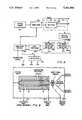
- FIG. 8depicts one embodiment of an optical transmission or distribution system constructed in accordance with the teachings of this invention.
- FIG. 9is one embodiment of a traveling wave balanced-bridge interferometer suitable for use in accordance with the teachings of this invention.
- FIG. 10is one embodiment of a synchronous harmonic detector suitable for use as one or both detectors 907 and 908 of FIG. 8;
- FIG. 11is a diagram of another embodiment of a transmission or distribution system constructed in accordance with the teachings of this invention.
- FIG. 12is one embodiment of an odd-wave linearizer circuit suitable for use in accordance with the teachings of this invention.
- FIGS. 13a, 13b, and 13cdescribe three embodiments of this invention utilizing predistortion networks
- FIG. 14is a model useful for analyzing the embodiment of FIG. 13c
- FIG. 15is a schematic diagram of one embodiment of a circuit suitable for use as the embodiment of FIG. 13b;
- FIG. 16is an embodiment of the topology of FIG. 13c
- FIG. 17is a model of the circuit of FIG. 16 useful for analysis
- FIGS. 18a, 18b, and 18care graphs depicting the odd-wave transfer characteristic of equation 69.
- FIG. 19is a diagram depicting one embodiment which utilizes a plurality of pilot tones.
- the solutions provided by this invention for linearizing the response of electro-optic modulatorsare of great interest to the cable television industry in its attempt to expand its networks and reduce prices by cutting down on maintenance expenses and to bring high-definition television (HDTV) to customers.
- the solutions provided by this inventionare also of great interest to the telephone industry in its attempt to bring broadband ISDN services over optical fiber to the homes of residential customers.
- the inventiondiscloses a general technique of taking advantage of the stability and repeatability of the modulator transfer characteristic in order to correct for second and third order distortion. These objectives are achieved in a way compatible with the nature of the video distribution frequency formats.
- the method of this invention for linearizing the amplitude transfer characteristic of integrated optic devices for analog transmissionis accomplished by injecting a pilot signal, monitoring the harmonic distortion content of the optical output, and feeding back bias signals to parametrically tune the operating points of the integrated optic modulator and of a predistortion network.
- General principles for realizing suitable parametrically tunable predistortion networksare also presented.
- FIG. 8depicts one embodiment of an optical transmission or distribution system constructed in accordance with the teachings of this invention which is suitable for distribution of broadband analog electronic signals.
- Transmitter system 900includes modulator means 902, a fiber optic distribution network 903 including one or more splitters 904, and at least one optical receiver 905.
- the composite video signal in a cable TV distribution system and in off the air TV broadcast systemsis a highpass signal starting at 54 MHz, with the individual AM/VSB modulated video channels stacked in frequency at intervals of 6 MHz (except for some frequency gaps used for FM radio, mobile radio, etc.)
- the low-pass vacant region(e.g. from 0 to 54 MHz in USA Cable Systems) of multichannel analog transmission (or other vacant spectral regions such as gaps between channel groups) is utilized for transmitting one or more pilot tones generated by pilot tone oscillator 910, which are used to monitor the presence of second and third order distortion, via second order distortion detector 907 and third order distortion detector 908 respectively.
- Signals from detectors 907 and 908 resulting from the monitoring of the pilot tones at the receiversare fed back, via loop processor 909, to modulator driver 906 in order to hold modulator 902 at the quadrature bias operating point, to the effect of eliminating or reducing second order distortion, and to parametrically tune non-linear predistortion circuits within modulator driver 906 in order to eliminate or reduce its inherent second order distortion and eliminate or reduce third-order distortion and second order distortion of the overall system by generating opposing distortions in modulator 902 and in the compensating non-linearity within modulator driver 906.
- the adaptive parametric feedback solution taught in this inventionprovides a consistent solution to the problem of improving non-linearity of electro-optic modulators for analog transmission as required for distribution of video signals via fiber optics and other emerging applications.
- the combined effect of the anti-distortion measures of this inventionis to reduce the overall non-linearity of the optical analog transmitter to the degree that cable television system specifications of composite second order and composite triple beat are met for higher modulation indexes, i.e., for higher signal to noise ratios.
- transmitter 900 of this inventionincludes a continuous wave laser, such as a DBF semiconductor laser or a solid state diode pumped laser, or an external cavity or a semiconductor Fabri-Perot laser serving as optical source 901.
- the output of optical source 901is fed into modulator means 902, which may be, for example, an electro-optic Mach-Zehnder modulator, directional coupler, balanced bridge interferometer, or more generally any suitable modulating means.
- Modulating means 902is electrically driven by modulation driver 906 which serves several functions:
- Modulation driver 906linearly amplifies the information signal and feeds the result to modulating means 902 conditioned at the proper level in amplitude and in impedance.
- Modulation driver 906provides a DC or slowly varying control voltage which establishes the modulator bias point. This slowly varying control voltage is used to steer modulating means 902 to the quadrature point where the second-order derivative of the transfer characteristic is nulled out.
- a typical embodimentas shown in FIG. 11, comprises a bias-tee circuit combining the AC and quasi-DC components while keeping the two paths mutually isolated. The bias-tee circuit combines the quasi-DC control voltage with the broadband information voltage (i.e., the composite video signal in the case of CATV distribution).
- biasing electrodesare provided in the integrated optic modulator separate from the high frequency modulating electrodes. Unlike prior art where DC and high frequency signals are combined in one set of electrodes, the claimed embodiment results in separating the high-speed circuitry from the biasing electronics.
- the high frequency electrodesdo not have to carry any DC currents. In this case the modulation driver simply routes the quasi-DC signal to the biasing electrode.
- An embodiment for a travelling wave balanced bridge interferometeris shown in FIG. 9.
- Modulation driver 906provides a parametrically tunable non-linear predistortion to the useful information signal in order to compensate for the residual non-linearity of modulating means 902, after the modulating means is brought to the vicinity of the quadrature point.
- Parametrically tunablemeans that the quiescent operating points of the circuit (the parameters) can be tuned to affect the amounts of various orders of non-linearity.
- Modulation driver 906superposes one or more pilot signals from pilot tone oscillator 910 upon the electrical information signal, such that the spectrum of the pilot signal(s) and the second and third harmonics of the pilot spectral components fall outside the passband of the useful information signal to be distributed.
- the second and third harmonics of the spectral components of the pilot signal(s)are monitored at the output of optical receiver 905 by harmonic distortion detectors 907 and 908 and used to actuate the parameters of the modulation driver 906 in such a way that the overall second and third order distortion is nulled out.
- This parametric feedbackis a form of negative feedback technique, however the feedback is not applied in real-time to the fast varying information signal but rather it is slowly applied to the parameters controlling the overall nonlinearity of the system, in order to null the overall nonlinearity out.
- an optical splitteris placed upon at least one optical output of modulating means 902 to route a portion of the transmitted optical power to a monitoring optical receiver (which can be thought of as part of transmitter 899).
- Optical splitter 904can, for example, be realized either as a fiber optic directional coupler or be integrated on the same integrated optic substrate with the modulating means 902, or be realized as a bulk optic beam splitter.
- Monitoring optical receiver 905feeds its output signal into two synchronous harmonic detectors 907 and 908, which detect the presence in the optical output of modulating means 902 of second and third harmonic spectral components of the pilot tone, respectively.
- the detectorsdetect the presence of intermodulation tones corresponding to the pilot tones.
- Synchronous harmonic detector 1000comprises lock-in detector 1001, formed by mixer 1002 followed by low-pass filter 1003.
- Mixer 1002multiplies the signals received on its two inputs, i.e. the electronic signal from monitoring optical receiver 905 (FIG. 8) and a reference signal at a harmonic or intermodulation tone of the pilot tone(s).
- the reference signalis phased by phase-shifter 1004 such that it is in phase with the harmonic to be monitored.
- the use of phase-shifter 1004is optional; at low frequencies the delay in the system may be small enough such that no substantial phase-shift occurs and all the signals are in phase.
- the harmonics of the pilot tone signalare thus detected using well known coherent or synchronous detection techniques, for example as described by R. Higgins, "Electronics with Digital and Analog Integrated Circuits," Hall, 1983, particularly Chapter 18, Section 3.
- two such synchronous harmonic detectors 907 and 908are provided to detect the second and third harmonic or intermodulation content, respectively, in the output from monitor optical receiver 905.
- Second order distortion detector 907has its reference signal at twice the fundamental frequency of the pilot tone
- third order distortion detector 908has its reference signal at three time the fundamental frequency of the pilot tone.
- the output signals of distortion detectors 907 and 908are fed into loop processor 909 which serves to electronically process the output signals from harmonic detectors 907 and 908 (either analog, digital or mixed analog-digital processing) in order to generate several analog actuating signals which are fed to modulation driver 906.
- the two harmonic detector signalsare processed separately, however one can envision more complex versions of analog processing, wherein the two harmonic detector signals are combined to generate at least two actuating signals.
- the loop networkis a two-port network with cross-coupling between the inputs and outputs, i.e. each of the outputs is a function of both inputs.
- the actuating signals provided by loop processor 909parametrically tune the quiescent point bias parameters of the modulation 906 driver, which in turn assures modulating means 902 continually operates at a bias point such that the overall distortion of the system is greatly reduced or eliminated as compared with prior art systems in which a bias point is chosen and remains fixed.
- this pilot signal provided by pilot tone oscillator 910can in general be any periodic signal which has null second and third harmonics such that the presence of the second and third harmonics in the optical output be uniquely associated with the degree of nonlinearity to be compensated, i.e., if one detects second or third harmonics in the output signal at the optical receiver, one knows that the harmonics are due to the combination driver-modulator, rather than originating in the pilot tone signal. Once one detects harmonics, corrections are applied to the driver to cause harmonics to disappear from the output signal of the optical receiver. It is also required that the frequency values of the (absent) second and third harmonics of the pilot tone fall within stop-bands of the information signal spectrum.
- the fundamental frequency of the pilot toneis less than 54 MHz/3, such that the second and third harmonics of the pilot tone fall in the low-pass stopband of 0 to 54 MHz, where there are no TV channels.
- the second and third harmonics of the pilot tonemust not fall on top of the intermodulation tones generated by the information signal itself in order not to contaminate the diagnostic signal with randomly phased spurious intermodulation tones associated with the information signal.
- pilot signal suitable for use with this invention when a single pilot tone is usedis a pure sinusoidal tone with its second and third harmonics kept at negligible level.
- Other pilot tone signalsincluding digitally generated signals, can be used consistent with the requirement that the second and third harmonics of the signal be null.
- Either of these two values for f.sup.(2)may be used diagnostically to provide parametric feedback by detecting the presence of a tone at f.sup.(2) at the output of the monitoring receiver The detection is done as before with a synchronous detector which is labeled "second-order distortion detector".
- the synchronous detectoris also provided a reference signal at the frequency f.sup.(2).
- This reference signalmay be derived from the two oscillators generating the two pilot tones by mixing those two tones in a strong non-linearity such as a mixer, and narrow-band passing the desired frequency f.sup.(2).
- an error signal proportional to the strength of the third order residual nonlinearity of the transmittermay be derived by monitoring a third order intermodulation tone generated by the two pilot tones at frequency
- FIG. 19shows an extension of the above concepts three pilot tones at frequencies f 1 p , f 2 p , f 3 p injected into the modulation signal.
- the intermodulation frequenciesare now
- indexes i,j, and kare taken from the set ⁇ 1,2,3 ⁇ and where i,j, and k do not have to be distinct.
- the reference frequencies f.sup.(2) and f.sup.(3)are derived by passing the summation of the three pilot tones through a strong non-linearity such as a diode or a mixer with its two input ports shorted and connected to the input signal.
- the other output of the optical splitter(the one which does not lead to the monitoring receiver) as well as any other available outputs of the modulation means, are connected to a fiber optic or free space transmission or distribution network terminating in one or more optical receivers. It is assumed that these receivers as well as the monitoring optical receiver within the transmitter contribute an amount of harmonic distortion and intermodulation which is substantially lower than that resulting from the transmitter nonlinearity.
- the loop processor 909consists of two uncoupled low-pass filters 1101 and 1102, each connected to the second and third distortion detectors 907, 908, (FIG. 8), respectively.
- either one of filters 1101 and 1102may be absent or included within its associated harmonic detectors 907 and/or 908.
- the output signal of second order distortion monitoring filter 1101drives the input 1103 to modulation driver 906 which is used to add a DC bias to the modulation signal applied to modulating means 902 or to directly control separate biasing electrodes on modulator means 902, in effect (ideally) nulling the amount of second order distortion present in the modulated output signal of modulating means 902 by shifting the bias point around the quadrature point.
- the output signal 1104 of third order distortion monitoring detector 1102drives a parametric input 1105 of linearizer predistortion circuit 1106, or alternatively drives gain control input 1107 of linear gain element 1108 placed after the linearizer circuit and before the modulating means 902.
- the parametric feedback loopactuates input 1104 to (ideally) null out the third order combined nonlinearity of the modulating driver 906 and the modulating means 902.
- the amount of third order nonlinearity of this circuitis parametrically controlled by a parametric electrical input (voltage or current) p, where in general the parameters ⁇ 1 and ⁇ 3 have different dependences on the control signal p.
- the sign of the third order coefficient ⁇ 3should be opposite that of the third order coefficient of the modulator and a certain relationship should exist between the various coefficients, such that for a particular value of the control parameter p, the third order nonlinearity of the odd-wave linearizer precisely compensates for the third-order nonlinearity of the modulator.
- the amount of third order nonlinearity of the odd-wave linearizeris tuned by the control circuit to precisely compensate for the third order nonlinearity of the modulator, nulling the overall third-order nonlinearity of the linearizer-modulator combination.
- the compensation processcan be described mathematically as follows:
- the gain Gmay be tuned to a value which may facilitate meeting the nulling condition. More generally, another parameter p' may be used to tune this gain in addition to or in lieu of p, yielding the following null third harmonic condition ##EQU8##
- the modulatoris described by a nonlinear transfer characteristic which is odd i.e. it has no second order coefficient. This is separately achieved by the control loop which monitors the generation of second harmonic distortion and superposes a slowly varying (quasi-DC) correction term onto the modulating input signal applied to the modulator.
- the slowly varying actuating voltagetunes the bias point of the modulator to the point of null second harmonic distortion.
- the modulator voltage v(t)include a pilot term v p cos ⁇ p t.
- the result of the second order non-linearity term ⁇ b v 2 (t)(eqs. 2,3,4) is to generate a term ⁇ b v p 2 cos2w p t, which is down converted by multiplication with the reference frequency v r cos(2w p t + ⁇ r ), to yield a signal ⁇ b v p 2 v r cos ⁇ r .
- this correction signalis proportional to the deviation ⁇ b away from the wanted quadrature point and has different signs depending whether the modulator drifts on one side or the other of the null point, thus it is a good error signal for actuating feedback to null ⁇ b , which results in elimination of the second harmonic component in the optical output.
- the modulatoris kept locked to its quadrature point, resulting in minimization of the second order harmonic and intermodulation distortion.
- the non-linear predistortion circuit described in FIG. 11provides a non-linear circuit 1106 which, combined with the nonlinearity of the modulator, provides a reduced (or ideally, a null) overall third order harmonic coefficient, as explained above.
- the transfer characteristic of the non-linear predistortion meansis designed to be as close as possible to the inverse of the non-linear characteristic of the modulating means, resulting in a partial cancellation of third order non-linearity.
- the predistortion circuitis realized with a degree of freedom, namely a parametric input which controls the relative values of the fundamental to the third harmonic output, (eq. 10) or a variable gain parameter (eq. 16).
- An odd-wave linearizer nonlinear circuitcan be designed based on a number of circuits which include nonlinear components such as diodes. Using antisymmetrical topologies, these circuits are designed to yield an ideally antisymmetric voltage or current transfer characteristic, however because of imperfections in element matching, residual even components may be present.
- a circuit with two degrees of freedomshould be designed which has its second and third order nonlinearity separately voltage or current controlled by two separate inputs. Such circuit should be embedded in a system which acts to null out the second harmonic characteristics. A particular implementation of such a system is described below with reference to FIG. 12. The transfer characteristic of the predistortion network is given by
- p 2the control parameter of the second harmonic coefficient
- p 3the control parameter of the third harmonic coefficient.
- the combined operation of all the control loops described aboveis that the last described control system makes sure that the linearizer is described by a characteristic which is entirely odd.
- the second harmonic monitor on the optical outputbrings the modulator to a null point of its second harmonic and the third harmonic monitor on the optical output brings the linearizer to an operating point where it has no second harmonic and its third order nonlinearity cancels that of the modulator. This results ideally in null overall second and third order distortion.
- the linearizer and modulatorwere described in eqs. 6,7 as having a memoriless instantaneous amplitude transfer characteristic. In reality, these devices have finite bandwidths and associated frequency responses. An important point is that the phase characteristic of the frequency response should be linear in frequency to a good approximation and the magnitude roll-off of the linearizer-modulator combination should be minimized. These requirements essentially mean that special care should be taken in using high frequency components in the linearizer non-linear predistortion circuit and using a broadband modulator. The more the phase frequency deviates from linearity and the amplitude rolls-off, the less perfect is the cancellation of third harmonic distortion in the combination of linearizer and modulator. This degradation may be counteracted by introducing linear frequency compensation circuits between the linearizer and the modulator, such that the overall frequency response is flat in magnitude and has constant group delay (linear phase) to a good approximation.
- the output y'(t) of the first non-linearity(eq. 18) contains the term
- the frequencies k,m,nmay or may not be distinct.
- the various complex exponentialsget multiplied by the complex transfer function H(w), i.e., get modified in amplitude and attenuated in phase:
- the intermodulation termevolves out of the linear filter as
- intermodulation termtransparently passes through the linear part of the modulator non-linearity yielding a component:
- the direct modulation termsinteract with the non-linearity of the modulator to generate intermodulation terms:
- the total intermodulation term at the output of the modulatoris the superposition of the two intermodulation terms generated in the linearizer and modulator respectively:
- the condition for broadband cancellation of non-linearityis the constancy of the amplitude frequency response over frequency as well as constancy of the group delay which is defined as the derivative of the phase response with respect to frequency:
- condition of eq. 27means that T g is constant over frequency.
- a modulator and linearizing circuitwhich have broad frequency responses, ideally much broader than the bandwidth of the information signal, such that the roll-off of the amplitude and group delay over frequency is negligible over the bandwidth of the information signal.
- the pre-distortion circuitis preferably realized by using an integrated electronics high frequency fabrication process which allows a high value of the frequency cut-off of the circuit elements.
- the frequency response requirementsare difficult to meet for state-of-the-art travelling wave modulators which exhibit a fairly constant group delay but may roll off in magnitude of the order of 1 dB over 1 GHz when designed for low drive voltage.
- the equalizationshould typically be realized by a high-pass or a band-pass filter which in the case of travelling wave LiNbO 3 modulators should provide an increase in amplitude in frequency while substantially providing linear phase (constant group delay) over the bandwidth of the information signal since the modulator response typically has constant group delay to start with as does the response of a linearizer predistortion network realized as an IC with a frequency cut-off substantially higher than the information bandwidth.
- the linear frequency equalizationmay be combined with tunable gain element 1108 (FIG. 11).
- the linearizeris not precisely odd-wave, there is an even second order residual coefficient ⁇ 2 . If no measures are taken to null out this coefficient, it turns out that the system as described above may still work over a range of parameters. In this case, the second-order harmonic monitoring loop is feeding back to the modulator but it now no longer brings the modulator to the quadrature point. It rather acts to null out the second order characteristics of the whole system--modulator plus linearizer by bringing the modulator to an operating point slightly off quadrature such that the residual second order distortion of the modulator cancels that of the linearizer circuit.
- the second order term nulling conditionmay be written ##EQU10## where q is the biasing control parameter of the modulator around its quadrature point.
- the tuningmay be done mainly or exclusively by means of the parameter q which controls the quadrature point of the modulator, i.e. q mainly affects ⁇ 2 and to a very small extent (for small deviations around quadrature) the linear gain ⁇ 1 .
- this tuningmay be performed or facilitated by means of a linear gain G which is inserted between the linearizer and the modulator. It is easy to see that a system ( ⁇ 1 , ⁇ 2 , ⁇ 3 ) followed by a gain G is equivalent to a system (G ⁇ 1 , G ⁇ 2 , G ⁇ 3 ).
- the third order nulling conditionbecomes identical to the one discussed before in the odd-wave case (eq. 37 reduces to eq. 9).
- soluble operating rangescan be more readily attained for the third order nulling condition by tuning the gain G to an appropriate value, which changes the nulling condition to
- the linearizer system included in the modulation driveris based on non-linear circuits or networks that should be tunable around the quiescent point where the second order Taylor series coefficients null out. These non-linear circuits should also have tunable third order coefficients (to be tuned by parametric feedback to such values as to cancel out the third-order coefficient of the modulator). Such tunabilities are the basis for the parametric feedback techniques outlined in this invention, in the wake of device to device variations and device drifts over time, temperature, optical power and the like.
- a predistortion network nominally odd-wavei.e., the predistortion network should ideally have an odd-wave characteristic (the output should be an anti-symmetric (odd) function of the input).
- Such a networkmay be realized using (anti)-symmetric circuit topologies in which two essentially identical sub-networks which are mirror images of each other are combined in certain ways in order to generate the odd-wave characteristic by superposition. Three separate embodiments are described as shown in FIGS. 13a, 13b, and 13c.
- FIG. 13aIn the first embodiment (FIG. 13a) two nominally identical one-ports are connected in series, inverted with respect to each other between the source and the load (the load may be preceded by a coupling network).
- the two "half-networks"are assumed nominally (i.e., ideally) matched but due to device variations and drifts slight differences may result in their characteristics. In the wake of mismatch between the half-networks, one can still recover an overall odd-wave characteristic for the whole system by slightly detuning of the biasing networks away from the nominally identical quiescent points.
- V 10 and V 20are the one-port voltages referred to a reference frame rigidly connected to the one-ports.
- the currents in the reference frames of the one-portsare given by I 10 and I 20 such that
- the applied voltageis not equal to the voltage across the parallel connection of one-ports and the analysis gets slightly more complicated as the voltage drops across the source and load impedances have to be taken into account but the conclusions are essentially the same.
- each of the one-portscan consist of a diode in parallel with a resistor.
- the resulting networkcan be simplified (by combining the two resistors in parallel) to that of FIG. 15.
- the capacitors and the inductorsare added for biasing purposes to block the DC and AC currents respectively.
- the circuitis controlled by the three biasing voltages V 1 , V 2 , V 3 .
- the resistorprovides a linear path for the signal, providing a sizable g 1 coefficient, while the diodes yield a small non-linear perturbation of an otherwise linear characteristic.
- V.sub. ⁇0 the sinh is antisymmetric and the cosh is symmetric, i.e., it contributes even components, however by tuning V.sub. ⁇ ⁇ 0 (achieved by tuning the voltage V 2 ) the system may be brought to antisymmetry as explained above in eqs. 54 and 55.
- the claimed inventionmay be further generalized to cover higher than third order terms by including harmonic detectors to monitor the higher order harmonics and intermodulation tones and feeding to control parameters which affect the relative magnitudes of higher order coefficients.
- Another application of the claimed inventionis to systems which use direct modulation of the light source rather than external modulation.
- the description aboveliterally applies for direct modulation around an inflection point of the light vs. current characteristic of a laser source. If no such operating point can be found then the mode of operation described in the last section applies, with the linearizer detuned away from the odd-wave operating point in such a way that the second order term of the linearizer nulls out the second order term of the laser (in the external modulation case, the modulator was tuned so as to null out the linearizer, here the cause-effect roles of linearizer and optical source are reversed but the mathematics is the same).
Landscapes
- Physics & Mathematics (AREA)
- Engineering & Computer Science (AREA)
- Computer Networks & Wireless Communication (AREA)
- Signal Processing (AREA)
- Electromagnetism (AREA)
- Optics & Photonics (AREA)
- Nonlinear Science (AREA)
- Optical Communication System (AREA)
Abstract
Description
f.sup.(3) =2f.sub.1.sup.p ±f.sub.2.sup.p or
f.sup.(3) =f.sub.1.sup.p ±2f.sub.2.sup.p
f.sup.(2) =f.sub.i.sup.p ±f.sub.j.sup.p ±f.sub.k.sup.p,
y(t)=α.sub.1 (p)x(t)+α.sub.3 (p)x.sup.3 (t) (6)
z(t)=β.sub.1 y(t)+β.sub.3 y.sup.3 (t) (7)
z=β.sub.1 α.sub.1 x+(β.sub.1 α.sub.3 +β.sub.3 α.sub.1.sup.3)x.sup.3 (8)
y'(t)=α.sub.1 (p)x(t)+α.sub.3 (p)x.sup.3 (t) (11)
y(t)=Gy'(t) (12)
z(t)=β.sub.1 y(t)+β.sub.3 y.sup.3 (t) (13)
y=α.sub.1 x+α.sub.2 (p.sub.2)x.sup.2 +α.sub.3 (p.sub.3)x.sup.3, (17)
y'(t)=α.sub.1 x(t)+α.sub.3 x.sup.3 (t) (18)
y(t)=h(t)* y'(t) (19)
z(t)=β.sub.1 y(t)+β.sub.3 y.sup.3 (t) (20)
α.sub.3 e.sup.j[±w.sbsp.k.sup.±jw.sbsp.m.sup.±w.sbsp.n.sup.]
α.sub.1 e.sup.±jw.sbsp.k.sup.t,
α.sub.1 e.sup.±jw.sbsp.m.sup.t,
α.sub.1 e.sup.±jw.sbsp.n.sup.t.
α.sub.3 H(±w.sub.k ±w.sub.m ±w.sub.n)e.sup.j[±w.sbsp.k.sup.±w.sbsp.m.sup.±w.sbsp.n.sup.]
α.sub.1 H(±w.sub.k)e.sup.±jw.sbsp.k.sup.t,
α.sub.1 H(±w.sub.m)e.sup.±jw.sbsp.m.sup.t,
α.sub.1 H(±w.sub.n)e.sup.±jw.sbsp.n.sup.t.
β.sub.1 α.sub.3 H(±w.sub.k ±w.sub.m ±w.sub.n)e.sup.j[±w.sbsp.k.sup.±w.sbsp.m.sup.±w.sbsp.n.sup.](21)
α.sub.1.sup.3 β.sub.3 H(±w.sub.k)H(±w.sub.m)H(±w.sub.n)e.sup.j[±w.sbsp.k.sup.±w.sbsp.m.sup.±w.sbsp.n.sup.] (22)
[β.sub.1 α.sub.3 H(±w.sub.k ±w.sub.m ±w.sub.n)+α.sub.1.sup.3 β.sub.3 H(±w.sub.k)H(±w.sub.m)H(±w.sub.n)]e.sup.j[±w.sbsp.k.sup.±jw.sbsp.m.sup.±w.sbsp.n.sup.] (23)
β.sub.1 α.sub.3 H(±w.sub.k ±w.sub.m ±w.sub.n)+α.sub.1.sup.3 β.sub.3 H(±w.sub.k)H(±w.sub.m)H(±w.sub.n)=0 (24)
β.sub.1 α.sub.3 +α.sub.1.sup.3 β.sub.3 =0(25)
β.sub.1 α.sub.3 A(±w.sub.k ±w.sub.m ±w.sub.n)e.sup.jφ[±w.sbsp.k.sup.±w.sbsp.m.sup.±w.sbsp.n.sup.] +
α.sub.1.sup.3 β.sub.3 A(±w.sub.k)
A(±w.sub.m)A(±w.sub.n)e.sup.j[φ[±w.sbsp.k.sup.]+φ[±w.sbsp.m.sup.]+φ[±w.sbsp.n.sup.]] =0 (26)
φ(w)=T.sub.g w (27)
φ[±w.sub.k ±w.sub.m ±w.sub.n ]=φ[±w.sub.k ]+φ[±w.sub.m ]+φ[±w.sub.n ] (28)
β.sub.1 α.sub.3 A(±w.sub.k ±w.sub.m ±w.sub.n)=-α.sub.1.sup.3 β.sub.3 A(±w.sub.k)A(±w.sub.m)A(±w.sub.n) (29)
β.sub.1 α.sub.3 +α.sub.1.sup.3 β.sub.3 G.sup.2 =0(30)
T.sub.g (w)=dφ/dw
y=α.sub.1 x+α.sub.2 x.sup.2 +α.sub.3 x.sup.3(31)
z=β.sub.1 y+β.sub.2 y.sup.2 +β.sub.3 y.sup.3(32)
Thus, ##EQU9## The nulling condition for the second order term x.sup.2 is
β.sub.1 α.sub.2 +β.sub.2 α.sub.1.sup.2 =0(34)
β.sub.1 α.sub.3 +β.sub.3 α.sub.1.sup.3 +2α.sub.1 α.sub.2 β.sub.2 =0 (35)
β.sub.1 α.sub.3 G+β.sub.3 α.sub.1.sup.3 G.sup.3 +2α.sub.1 α.sub.2 β.sub.2 G.sup.2 =0 (38)
β.sub.3 α.sub.1.sup.3 G.sup.2 +2α.sub.1 α.sub.2 β.sub.2 G+β.sub.1 α.sub.3 =0 (39)
α.sub.1.sup.2 α.sup.2.sub.2 β.sub.2.sup.2 -β.sub.3 α.sub.1.sup.3 β.sub.1 α.sub.3 >0 (40)
I=I.sub.1 +I.sub.2 (41)
V=V.sub.10 -V.sub.20 (42)
I.sub.1 =I.sub.10 (43)
I.sub.2 =-I.sub.20 (44)
I=I.sub.10 (V)-I.sub.20 (-V) (45)
I.sub.10 ()=I.sub.20 ()≡I.sub.0 () (46)
I(V)=I.sub.0 (V)-I.sub.0 (-V) (47)
I(-V)=I.sub.0 (-V)-I.sub.0 (V)=-I(V) (48)
I.sub.10 (V)=α.sub.1 V+α.sub.2 V.sup.2 +α.sub.3 V.sup.3(49)
I.sub.10 (V)=α'.sub.1 V+α'.sub.2 V.sup.2 +α'.sub.3 V.sup.3(50)
I(V)=I.sub.10 (V)-I.sub.20 (-V)=(α.sub.1 +α'.sub.1)V+(α.sub.2 -α'.sub.2)V.sup.2 +(α.sub.3 +α'.sub.3)V.sup.3 (51)
g.sub.2 =α.sub.2 (p.sub.2)-α'.sub.2 (p'.sub.2)=0(52)
I(V)=g.sub.1 V+g.sub.2 V.sup.2 +g.sub.3 V.sup.3 (53)
I(V-Δ)=g.sub.3 V.sup.3 +[g.sub.2 -3g.sub.3 Δ]V.sup.2 +[g.sub.1 +3g.sub.3 Δ.sup.2 -2g.sub.2 Δ]V+[g.sub.1 Δ+g.sub.2 Δ.sup.2 +g.sub.3 Δ.sup.3 ] (54)
V.sub.1 -V.sub.2 =V+V.sub.Δ (57)
V.sub.2 -V.sub.3 =V-V.sub.Δ (58)
NV.sub.DB1 +MV.sub.DE1 -MV.sub.DE2 -NV.sub.DB2 =0 (61)
Claims (50)
Priority Applications (1)
| Application Number | Priority Date | Filing Date | Title |
|---|---|---|---|
| US07/685,966US5161044A (en) | 1989-07-11 | 1991-04-15 | Optical transmitters linearized by means of parametric feedback |
Applications Claiming Priority (2)
| Application Number | Priority Date | Filing Date | Title |
|---|---|---|---|
| US37832889A | 1989-07-11 | 1989-07-11 | |
| US07/685,966US5161044A (en) | 1989-07-11 | 1991-04-15 | Optical transmitters linearized by means of parametric feedback |
Related Parent Applications (1)
| Application Number | Title | Priority Date | Filing Date |
|---|---|---|---|
| US37832889AContinuation | 1989-07-11 | 1989-07-11 |
Publications (1)
| Publication Number | Publication Date |
|---|---|
| US5161044Atrue US5161044A (en) | 1992-11-03 |
Family
ID=27008170
Family Applications (1)
| Application Number | Title | Priority Date | Filing Date |
|---|---|---|---|
| US07/685,966Expired - LifetimeUS5161044A (en) | 1989-07-11 | 1991-04-15 | Optical transmitters linearized by means of parametric feedback |
Country Status (1)
| Country | Link |
|---|---|
| US (1) | US5161044A (en) |
Cited By (108)
| Publication number | Priority date | Publication date | Assignee | Title |
|---|---|---|---|---|
| WO1993010603A1 (en)* | 1991-11-19 | 1993-05-27 | Harmonic Lightwaves, Inc. | Shunt-expansive predistortion linearizers for optical analog transmitters |
| US5289252A (en)* | 1992-12-08 | 1994-02-22 | Hughes Aircraft Company | Linear frequency modulation control for FM laser radar |
| US5317443A (en)* | 1990-11-27 | 1994-05-31 | Fujitsu Limited | Optical transmitter |
| US5319489A (en)* | 1991-01-24 | 1994-06-07 | Alcatel N.V. | Method and apparatus for relative positioning of a frequency, in particular an optical frequency |
| US5321543A (en)* | 1992-10-20 | 1994-06-14 | General Instrument Corporation | Apparatus and method for linearizing an external optical modulator |
| US5347529A (en)* | 1992-08-07 | 1994-09-13 | Siemens Aktiengesellschaft | Method for generating a distortion-free, frequency-modulated optical signal and apparatus for the implementation of such a method |
| US5428314A (en)* | 1994-05-09 | 1995-06-27 | Tacan Corporation | Odd/even order distortion generator and distortion cancellation circuit |
| US5473460A (en)* | 1994-07-25 | 1995-12-05 | At&T Corp. | Adaptive equalizer for analog optical signal transmission |
| US5528405A (en)* | 1995-01-05 | 1996-06-18 | Harris Corporation | Power series correction in a linear fiber optic analog transmission system and method |
| US5532857A (en)* | 1994-09-07 | 1996-07-02 | Ael Industries, Inc. | Wide dynamic range optical link using DSSC linearizer |
| US5532867A (en)* | 1995-06-06 | 1996-07-02 | Hughes Aircraft Company | Bias stabilization circuit and method for a linearized directional coupler modulator |
| US5696859A (en)* | 1995-02-23 | 1997-12-09 | Fujitsu Limited | Optical-filter array, optical transmitter and optical transmission system |
| US5710653A (en)* | 1995-03-06 | 1998-01-20 | Fiber Optic Network Solutions Corp. | Linear multi-output optical transmitter system |
| US5781327A (en)* | 1996-08-19 | 1998-07-14 | Trw Inc. | Optically efficient high dynamic range electro-optic modulator |
| WO1998023064A3 (en)* | 1996-11-18 | 1998-08-06 | Ericsson Telefon Ab L M | Method and device for signal repetition |
| US5798854A (en)* | 1994-05-19 | 1998-08-25 | Ortel Corporation | In-line predistorter for linearization of electronic and optical signals |
| US5812297A (en)* | 1995-10-12 | 1998-09-22 | Pirelli Cavi S.P.A. | Bias system in an optical CATV modulator |
| US5850305A (en)* | 1996-12-18 | 1998-12-15 | Scientific-Atlanta, Inc. | Adaptive predistortion control for optical external modulation |
| US5872814A (en)* | 1997-02-24 | 1999-02-16 | At&T Wireless Services Inc. | Method for linearization of RF transmission electronics using baseband pre-distortion in T/R compensation pilot signals |
| US5875048A (en)* | 1995-03-06 | 1999-02-23 | Cfx Communication Systems,Llc | Linear multi-output optical transmitter system |
| US5881091A (en)* | 1996-02-05 | 1999-03-09 | Hewlett-Packard Company | Spread spectrum linearization for digitizing receivers |
| WO1999017410A1 (en)* | 1997-09-29 | 1999-04-08 | Corning Incorporated | Optical amplifier apparatus |
| RU2128885C1 (en)* | 1997-02-24 | 1999-04-10 | Военная академия Ракетных войск стратегического назначения им.Петра Великого | Fiber-optic information and diagnostic signal transmission system |
| US5953139A (en)* | 1996-03-06 | 1999-09-14 | Cfx Communications Systems, Llc | Wavelength division multiplexing system |
| DE19831715A1 (en)* | 1998-07-15 | 2000-01-20 | Alcatel Sa | Operating point setting of a diode of a diode network by voltage injection |
| US6111680A (en)* | 1997-12-01 | 2000-08-29 | Ebara Corporation | Transmitting a signal using duty cycle modulation |
| WO2000060734A1 (en)* | 1999-04-01 | 2000-10-12 | General Instrument Corporation | Non-linear distortion generator |
| WO2000060733A1 (en)* | 1999-04-01 | 2000-10-12 | General Instrument Corporation | Non-linear distortion generator for both second and third order distortion |
| US6178026B1 (en)* | 1997-06-02 | 2001-01-23 | Nec Corporation | Analog optical transmission apparatus |
| US6232817B1 (en) | 1998-07-15 | 2001-05-15 | Alcatel | Temperature stabilization of a predistorter with voltage supply |
| WO2001052442A1 (en)* | 2000-01-10 | 2001-07-19 | Airnet Communications Corporation | Method and apparatus for equalization in transmit and receive levels in a broadband transceiver system |
| EP0760184A4 (en)* | 1994-05-19 | 2001-08-08 | Ortel Corp | In-line predistorter for linearization of electronic and optical signals |
| US6288814B1 (en) | 1994-05-19 | 2001-09-11 | Ortel Corporation | In-line predistorter for linearization of electronic and optical signals |
| US6300817B1 (en) | 1998-07-15 | 2001-10-09 | Alcatel | Temperature stabilization of a predistorter |
| US6426822B1 (en)* | 1998-06-25 | 2002-07-30 | Ipicom, Inc. | Method and apparatus for reducing non-linear characteristics of a signal modulator by coherent data collection |
| US6466084B1 (en) | 2000-01-24 | 2002-10-15 | General Instrument Corporation | Circuit for reducing third order intermodulation distortion for a broadband RF amplifier |
| WO2002082693A1 (en)* | 2001-04-03 | 2002-10-17 | Lightwave Solutions, Inc. | Optical linearizer for fiber communications |
| US6509543B1 (en)* | 1998-03-10 | 2003-01-21 | Matsushita Electric Industrial Co., Ltd. | Semiconductor laser heating apparatus |
| US6509789B1 (en) | 2000-01-24 | 2003-01-21 | General Instrument Corporation | Circuit for reducing second and third order intermodulation distortion for a broadband RF amplifier |
| US6519066B2 (en)* | 2000-12-18 | 2003-02-11 | Nortel Networks Ltd | System level stimulated raman scattering (SRS) compensation |
| US6556728B2 (en)* | 1996-12-23 | 2003-04-29 | Tellabs Denmark A/S | Method and an apparatus for modulating light |
| US6563630B1 (en) | 1997-09-29 | 2003-05-13 | Corning Incorporated | Optical amplifier apparatus |
| US6570698B2 (en) | 2000-11-01 | 2003-05-27 | Electronics And Telecommunications Research Institute | Apparatus and method for modulating optical intensity with amplitude noise suppressed by using linear optical modulator |
| US6587243B1 (en) | 1999-12-10 | 2003-07-01 | General Instrument Corporation | Second order predistortor for a return laser transmitter |
| US20030147116A1 (en)* | 2002-02-01 | 2003-08-07 | Isaac Shpantzer | Method and apparatus for pulse generation and adaptive pulse generation for optical communications |
| US6626588B1 (en)* | 1999-02-15 | 2003-09-30 | Matsushita Electric Industrial Co., Ltd. | Optical transmission apparatus |
| US20030185575A1 (en)* | 2002-03-26 | 2003-10-02 | Fujitsu Limited | Drive control apparatus and drive control method for optical modulator |
| EP0845880A3 (en)* | 1996-11-29 | 2004-01-02 | Matsushita Electric Industrial Co., Ltd. | Optical transmission device and system |
| US20040008083A1 (en)* | 2002-07-09 | 2004-01-15 | General Instrument Corporation | Inline predistortion for both CSO and CTB correction |
| US6687466B1 (en)* | 2000-01-06 | 2004-02-03 | Adc Telecommunications, Inc. | Dynamic distortion control |
| US20040052536A1 (en)* | 2002-09-17 | 2004-03-18 | General Instrument Corporation | Second order predistortion circuit |
| US20040067064A1 (en)* | 2002-10-03 | 2004-04-08 | Nortel Networks Limited | Electrical domain compensation of optical dispersion in an optical communications system |
| US20040105627A1 (en)* | 2002-11-15 | 2004-06-03 | Jds Uniphase Corporation | Receiver optical sub-assembly |
| US20040218931A1 (en)* | 2003-05-01 | 2004-11-04 | Optium Corporation | Linearized Optical Transmitter Using Feedback Control |
| US20040240765A1 (en)* | 2003-05-30 | 2004-12-02 | Jds Uniphase Corporation | Optical digital external modulator |
| WO2004112286A1 (en)* | 2003-06-13 | 2004-12-23 | Matsushita Electric Industrial Co., Ltd. | Optical transmission system; and transmitter, receiver and signal level adjustment method for use therein |
| US20050047796A1 (en)* | 2003-08-28 | 2005-03-03 | Harres Daniel N. | RF photonics residual error correction |
| US20050105917A1 (en)* | 2003-11-14 | 2005-05-19 | Hidehiko Narusawa | Optical modulating apparatus |
| US6931214B1 (en) | 2000-05-10 | 2005-08-16 | Tellabs Operations, Inc. | Method and apparatus for maintaining a pre-determined ratio of a pilot tone power and a mean optical output power of an optical signal |
| US20050220458A1 (en)* | 2004-04-02 | 2005-10-06 | K2 Optronics, A Delaware Corporation | Analog transmitter using an external cavity laser (ECL) |
| US20050271396A1 (en)* | 2004-03-19 | 2005-12-08 | John Iannelli | Directly modulated laser optical transmission system |
| US20060018583A1 (en)* | 2004-05-05 | 2006-01-26 | Iannelli John M | Method and apparatus for distortion control for optical transmitters |
| US7016607B1 (en) | 1998-12-14 | 2006-03-21 | Tellabs Operations, Inc. | Methods and apparatus for optical network management using pilot tones |
| US20060088251A1 (en)* | 2004-10-15 | 2006-04-27 | Xiaozhong Wang | Integrated optical fiber and electro-optical converter |
| US20060210282A1 (en)* | 2005-03-15 | 2006-09-21 | John Iannelli | Directly modulated laser optical transmission system with phase modulation |
| US20060222004A1 (en)* | 2005-04-01 | 2006-10-05 | International Business Machines Corporation | Methods and apparatus for transferring data |
| US20060239687A1 (en)* | 2005-02-23 | 2006-10-26 | Anand Gopinath | Optical fiber communication link |
| US20060251425A1 (en)* | 2004-12-23 | 2006-11-09 | K2 Optronics | Suppression of fiber-induced noise caused by narrow linewidth lasers |
| US7199446B1 (en) | 2003-02-18 | 2007-04-03 | K2 Optronics, Inc. | Stacked electrical resistor pad for optical fiber attachment |
| US20070086789A1 (en)* | 2005-10-18 | 2007-04-19 | Fujitsu Limited | Chirp switching circuit and optical transmission system |
| US7212326B2 (en) | 2003-05-30 | 2007-05-01 | Jds Uniphase Corporation | Optical external modulator |
| US20070098417A1 (en)* | 2005-10-27 | 2007-05-03 | Eva Peral | Distortion cancellation circuitry for optical receivers |
| US20070206962A1 (en)* | 2006-03-02 | 2007-09-06 | Emcore Corporation | Externally modulated laser optical transmission system with feed forward noise cancellation |
| US20070206961A1 (en)* | 2006-03-02 | 2007-09-06 | Emcore Corporation | Directly modulated or externally modulated laser optical transmission system with feed forward noise cancellation |
| US20070206956A1 (en)* | 2004-11-11 | 2007-09-06 | Koji Kikushima | Optical Transmitting Device, Optical Transmission System, Optical Transmitting Method And Optical Transmission Method |
| US20070297803A1 (en)* | 2006-06-21 | 2007-12-27 | Eva Peral | In-line distortion cancellation circuits for linearization of electronic and optical signals with phase and frequency adjustment |
| US7426350B1 (en)* | 2001-10-26 | 2008-09-16 | Cisco Technology, Inc. | Hybrid optical and electrical fiber optic link linearizer |
| RU2362271C1 (en)* | 2007-11-01 | 2009-07-20 | Открытое акционерное общество "Информационные телекоммуникационные технологии" (ОАО "Интелтех") | Fibre-optic transmission system for detecting attempts at unauthorised access |
| US20090237767A1 (en)* | 2008-03-17 | 2009-09-24 | Arris | Predistortion using fpga |
| US20100067902A1 (en)* | 2008-09-16 | 2010-03-18 | Nortel Networks Limited | Optical transmitter error reduction using receiver feedback |
| RU2400933C1 (en)* | 2009-02-24 | 2010-09-27 | Федеральное государственное учреждение "Государственный научно-исследовательский испытательный институт проблем технической защиты информации Федеральной службы по техническому и экспортному контролю" | Method of information transfer in fibre optic system of data transfer with spectral multiplex |
| US20100312828A1 (en)* | 2009-06-03 | 2010-12-09 | Mobixell Networks Ltd. | Server-controlled download of streaming media files |
| RU2421912C2 (en)* | 2008-08-01 | 2011-06-20 | Нек Корпорейшн | Device of optical communication, system of optical communication, method and programme to control output of optical signals |
| RU2428798C2 (en)* | 2009-09-14 | 2011-09-10 | Владимир Васильевич Гришачев | Fibre optic detector of voice information leakage threats via fibre optic communications |
| US20110225315A1 (en)* | 2010-03-09 | 2011-09-15 | Mobixell Networks Ltd. | Multi-stream bit rate adaptation |
| RU2456748C1 (en)* | 2011-03-18 | 2012-07-20 | Государственный научно-исследовательский испытательный институт проблем технической защиты информации Федеральной службы по техническому и экспортному контролю | Optic fibre transmission system with spectral multiplex |
| WO2012163419A1 (en)* | 2011-06-01 | 2012-12-06 | Telefonaktiebolaget L M Ericsson (Publ) | Modulator for optical transmitter |
| US8538272B1 (en)* | 2004-04-22 | 2013-09-17 | Ciena Corporation | Data security in optical communications systems |
| US20130284930A1 (en)* | 2012-04-25 | 2013-10-31 | Advantest Corporation | Measurement device, method, and recording medium |
| USRE44647E1 (en) | 2005-03-15 | 2013-12-17 | Emcore Corporation | Directly modulated laser optical transmission system with phase modulation |
| US8688074B2 (en) | 2011-02-28 | 2014-04-01 | Moisixell Networks Ltd. | Service classification of web traffic |
| US20140140707A1 (en)* | 2012-11-21 | 2014-05-22 | Fujitsu Limited | Optical transmission device, method of optical transmission, and non-transitory computer-readable medium |
| US8832709B2 (en) | 2010-07-19 | 2014-09-09 | Flash Networks Ltd. | Network optimization |
| US20140270807A1 (en)* | 2013-03-15 | 2014-09-18 | Meredith N. Hutchinson | System and method for suppression of even-order photodiode distortions |
| US8867928B2 (en) | 2010-05-17 | 2014-10-21 | Neophotonics Corporation | Hybrid fiber coaxial network optical transport system with distortion control |
| US20160050017A1 (en)* | 2014-08-13 | 2016-02-18 | Xilinx, Inc. | Adaptive optical channel compensation |
| US20170170993A1 (en)* | 2015-12-08 | 2017-06-15 | Zte Corporation | Training assisted joint equalization |
| US9819412B1 (en)* | 2016-05-04 | 2017-11-14 | Inphi Corporation | Transmitter gain imbalance and skew optimization for coherent transmitters |
| US20180076900A1 (en)* | 2015-03-20 | 2018-03-15 | Nec Corporation | Optical transmitter and optical communication method |
| DE112013003262B4 (en) | 2012-06-27 | 2018-05-03 | Analog Devices, Inc. | Digital predistortion |
| US9998216B2 (en)* | 2016-05-09 | 2018-06-12 | Fujitsu Limited | Skew measurement in an optical coherent transponder |
| US10148363B2 (en) | 2015-12-08 | 2018-12-04 | Zte Corporation | Iterative nonlinear compensation |
| US10348438B2 (en)* | 2017-09-04 | 2019-07-09 | Huawei Technologies Co., Ltd. | Spur removal in pilot-tone OPM |
| CN110048782A (en)* | 2019-05-15 | 2019-07-23 | 中国电子科技集团公司第三十四研究所 | A kind of intensity modulated directly detects the even-order harmonic in link and inhibits system |
| CN111200460A (en)* | 2018-11-19 | 2020-05-26 | 富士通株式会社 | Modulation depth monitoring device and method of jitter signal, and optical transmitter |
| US10976576B2 (en) | 2016-08-30 | 2021-04-13 | Halliburton Energy Services, Inc. | Bias control for downhole optical intensity modulators |
| US20240120996A1 (en)* | 2022-09-30 | 2024-04-11 | Fujitsu Limited | Optical transmitter and bias control method |
| WO2025054549A1 (en)* | 2023-09-07 | 2025-03-13 | AyDeeKay LLC dba Indie Semiconductor | Optical linearization technique |
Citations (3)
| Publication number | Priority date | Publication date | Assignee | Title |
|---|---|---|---|---|
| US4501022A (en)* | 1981-12-03 | 1985-02-19 | International Standard Electric Corporation | Optical transmission system and method |
| US4504976A (en)* | 1982-05-06 | 1985-03-12 | Societe Anonyme De Telecommunications | Device for regulating a laser diode |
| US4893300A (en)* | 1988-08-01 | 1990-01-09 | American Telephone And Telegraph Company | Technique for reducing distortion characteristics in fiber-optic links |
- 1991
- 1991-04-15USUS07/685,966patent/US5161044A/ennot_activeExpired - Lifetime
Patent Citations (3)
| Publication number | Priority date | Publication date | Assignee | Title |
|---|---|---|---|---|
| US4501022A (en)* | 1981-12-03 | 1985-02-19 | International Standard Electric Corporation | Optical transmission system and method |
| US4504976A (en)* | 1982-05-06 | 1985-03-12 | Societe Anonyme De Telecommunications | Device for regulating a laser diode |
| US4893300A (en)* | 1988-08-01 | 1990-01-09 | American Telephone And Telegraph Company | Technique for reducing distortion characteristics in fiber-optic links |
Non-Patent Citations (12)
| Title |
|---|
| "Comparison of Second and Third Order Distortion in Intensity Modulated InGaA: Lasers and an LiNbO3 External Modulator", Paper WK2, OFC89', Conference on Optical Fiber Communications, Houston, Tex., Feb. 1989. |
| "Feasibility of Multi-Channel VSB/AM Transmission on Fiber Optic Links", Jack Koscinski, General Optronics Corporation, pp. 1-9, Jan. 1987. |
| "High Sensitivity Optical Analog Link Using an External Modulator", by Betts et al., CLEO (1989) Apr. 24-28, Paper TUJ19. |
| "Optical Waves in Crystals", by Yariv et al., (Ch. 11: Guided Waves and Integrated Optics). |
| "Systems Characteristics of Direct Modulated and Externally Modulated RF Fiber Optic Links", by Stephens et al., Journal of Lightwave Technology, vol. LT-5. |
| "Titanium-Diffused Lithium Niobate Waveguide Devices", by R. C. Alferness, Guided-Wave Optoelectronics (1988). |
| Comparison of Second and Third Order Distortion in Intensity Modulated InGaA: Lasers and an LiNbO 3 External Modulator , Paper WK2, OFC89 , Conference on Optical Fiber Communications, Houston, Tex., Feb. 1989.* |
| Feasibility of Multi Channel VSB/AM Transmission on Fiber Optic Links , Jack Koscinski, General Optronics Corporation, pp. 1 9, Jan. 1987.* |
| High Sensitivity Optical Analog Link Using an External Modulator , by Betts et al., CLEO (1989) Apr. 24 28, Paper TUJ19.* |
| Optical Waves in Crystals , by Yariv et al., (Ch. 11: Guided Waves and Integrated Optics).* |
| Systems Characteristics of Direct Modulated and Externally Modulated RF Fiber Optic Links , by Stephens et al., Journal of Lightwave Technology, vol. LT 5.* |
| Titanium Diffused Lithium Niobate Waveguide Devices , by R. C. Alferness, Guided Wave Optoelectronics (1988).* |
Cited By (173)
| Publication number | Priority date | Publication date | Assignee | Title |
|---|---|---|---|---|
| US5317443A (en)* | 1990-11-27 | 1994-05-31 | Fujitsu Limited | Optical transmitter |
| US5319489A (en)* | 1991-01-24 | 1994-06-07 | Alcatel N.V. | Method and apparatus for relative positioning of a frequency, in particular an optical frequency |
| WO1993010603A1 (en)* | 1991-11-19 | 1993-05-27 | Harmonic Lightwaves, Inc. | Shunt-expansive predistortion linearizers for optical analog transmitters |
| US5282072A (en)* | 1991-11-19 | 1994-01-25 | Harmonic Lightwaves, Inc. | Shunt-expansive predistortion linearizers for optical analog transmitters |
| US5347529A (en)* | 1992-08-07 | 1994-09-13 | Siemens Aktiengesellschaft | Method for generating a distortion-free, frequency-modulated optical signal and apparatus for the implementation of such a method |
| US5321543A (en)* | 1992-10-20 | 1994-06-14 | General Instrument Corporation | Apparatus and method for linearizing an external optical modulator |
| US5289252A (en)* | 1992-12-08 | 1994-02-22 | Hughes Aircraft Company | Linear frequency modulation control for FM laser radar |
| AU650209B1 (en)* | 1992-12-08 | 1994-06-09 | Hughes Aircraft Company | Linear frequency modulation control for FM laser radar |
| US5428314A (en)* | 1994-05-09 | 1995-06-27 | Tacan Corporation | Odd/even order distortion generator and distortion cancellation circuit |
| US6288814B1 (en) | 1994-05-19 | 2001-09-11 | Ortel Corporation | In-line predistorter for linearization of electronic and optical signals |
| EP0760184A4 (en)* | 1994-05-19 | 2001-08-08 | Ortel Corp | In-line predistorter for linearization of electronic and optical signals |
| US5798854A (en)* | 1994-05-19 | 1998-08-25 | Ortel Corporation | In-line predistorter for linearization of electronic and optical signals |
| US5473460A (en)* | 1994-07-25 | 1995-12-05 | At&T Corp. | Adaptive equalizer for analog optical signal transmission |
| US5532857A (en)* | 1994-09-07 | 1996-07-02 | Ael Industries, Inc. | Wide dynamic range optical link using DSSC linearizer |
| US5528405A (en)* | 1995-01-05 | 1996-06-18 | Harris Corporation | Power series correction in a linear fiber optic analog transmission system and method |
| US5696859A (en)* | 1995-02-23 | 1997-12-09 | Fujitsu Limited | Optical-filter array, optical transmitter and optical transmission system |
| US5710653A (en)* | 1995-03-06 | 1998-01-20 | Fiber Optic Network Solutions Corp. | Linear multi-output optical transmitter system |
| US5875048A (en)* | 1995-03-06 | 1999-02-23 | Cfx Communication Systems,Llc | Linear multi-output optical transmitter system |
| US6163395A (en)* | 1995-03-06 | 2000-12-19 | Fiber Optics Network Solutions Corp. | Linear multi-output optical transmitter system |
| US5532867A (en)* | 1995-06-06 | 1996-07-02 | Hughes Aircraft Company | Bias stabilization circuit and method for a linearized directional coupler modulator |
| US5812297A (en)* | 1995-10-12 | 1998-09-22 | Pirelli Cavi S.P.A. | Bias system in an optical CATV modulator |
| US5881091A (en)* | 1996-02-05 | 1999-03-09 | Hewlett-Packard Company | Spread spectrum linearization for digitizing receivers |
| US5953139A (en)* | 1996-03-06 | 1999-09-14 | Cfx Communications Systems, Llc | Wavelength division multiplexing system |
| US5781327A (en)* | 1996-08-19 | 1998-07-14 | Trw Inc. | Optically efficient high dynamic range electro-optic modulator |
| WO1998023064A3 (en)* | 1996-11-18 | 1998-08-06 | Ericsson Telefon Ab L M | Method and device for signal repetition |
| EP0845880A3 (en)* | 1996-11-29 | 2004-01-02 | Matsushita Electric Industrial Co., Ltd. | Optical transmission device and system |
| US5850305A (en)* | 1996-12-18 | 1998-12-15 | Scientific-Atlanta, Inc. | Adaptive predistortion control for optical external modulation |
| US6810159B2 (en) | 1996-12-23 | 2004-10-26 | Tellabs Denmark A/S | Method and an apparatus for modulating light |
| US6556728B2 (en)* | 1996-12-23 | 2003-04-29 | Tellabs Denmark A/S | Method and an apparatus for modulating light |
| US20030202727A1 (en)* | 1996-12-23 | 2003-10-30 | Olesen Dennis S. | Method and an apparatus for modulating light |
| US5872814A (en)* | 1997-02-24 | 1999-02-16 | At&T Wireless Services Inc. | Method for linearization of RF transmission electronics using baseband pre-distortion in T/R compensation pilot signals |
| RU2128885C1 (en)* | 1997-02-24 | 1999-04-10 | Военная академия Ракетных войск стратегического назначения им.Петра Великого | Fiber-optic information and diagnostic signal transmission system |
| US6178026B1 (en)* | 1997-06-02 | 2001-01-23 | Nec Corporation | Analog optical transmission apparatus |
| US6563630B1 (en) | 1997-09-29 | 2003-05-13 | Corning Incorporated | Optical amplifier apparatus |
| WO1999017410A1 (en)* | 1997-09-29 | 1999-04-08 | Corning Incorporated | Optical amplifier apparatus |
| US6111680A (en)* | 1997-12-01 | 2000-08-29 | Ebara Corporation | Transmitting a signal using duty cycle modulation |
| US6509543B1 (en)* | 1998-03-10 | 2003-01-21 | Matsushita Electric Industrial Co., Ltd. | Semiconductor laser heating apparatus |
| US6426822B1 (en)* | 1998-06-25 | 2002-07-30 | Ipicom, Inc. | Method and apparatus for reducing non-linear characteristics of a signal modulator by coherent data collection |
| US6232817B1 (en) | 1998-07-15 | 2001-05-15 | Alcatel | Temperature stabilization of a predistorter with voltage supply |
| US6300817B1 (en) | 1998-07-15 | 2001-10-09 | Alcatel | Temperature stabilization of a predistorter |
| US6323726B1 (en) | 1998-07-15 | 2001-11-27 | Alcatel | Operating point adjustment for a diode of a diode network by means of voltage injection |
| DE19831715A1 (en)* | 1998-07-15 | 2000-01-20 | Alcatel Sa | Operating point setting of a diode of a diode network by voltage injection |
| US7376350B2 (en) | 1998-12-14 | 2008-05-20 | Tellabs Operations, Inc. | Methods and apparatus for optical network management using pilot tones |
| US7016607B1 (en) | 1998-12-14 | 2006-03-21 | Tellabs Operations, Inc. | Methods and apparatus for optical network management using pilot tones |
| US20060110158A1 (en)* | 1998-12-14 | 2006-05-25 | Carrick John C | Methods and apparatus for optical network management using pilot tones |
| US7123832B2 (en) | 1998-12-14 | 2006-10-17 | Tellabs Operations, Inc. | Methods and apparatus for optical network management using pilot tones |
| US6626588B1 (en)* | 1999-02-15 | 2003-09-30 | Matsushita Electric Industrial Co., Ltd. | Optical transmission apparatus |
| WO2000060734A1 (en)* | 1999-04-01 | 2000-10-12 | General Instrument Corporation | Non-linear distortion generator |
| WO2000060733A1 (en)* | 1999-04-01 | 2000-10-12 | General Instrument Corporation | Non-linear distortion generator for both second and third order distortion |
| US6570430B1 (en) | 1999-04-01 | 2003-05-27 | General Instrument Corporation | Non-linear distortion generator for both second and third order distortion |
| US6577177B2 (en) | 1999-04-01 | 2003-06-10 | General Instrument Corporation | Non-linear distortion generator |
| WO2000060735A1 (en)* | 1999-04-01 | 2000-10-12 | General Instrument Corporation | Non-linear distortion generator |
| US6587243B1 (en) | 1999-12-10 | 2003-07-01 | General Instrument Corporation | Second order predistortor for a return laser transmitter |
| US6687466B1 (en)* | 2000-01-06 | 2004-02-03 | Adc Telecommunications, Inc. | Dynamic distortion control |
| US7155132B2 (en) | 2000-01-06 | 2006-12-26 | Adc Telecommunications, Inc. | Dynamic distortion control |
| US20040109697A1 (en)* | 2000-01-06 | 2004-06-10 | Adc Telecommunications, Inc. | Dynamic distortion control |
| US20020090915A1 (en)* | 2000-01-10 | 2002-07-11 | Komara Michael A. | Method and apparatus for equalization in transmit and receive levels in a broadband transceiver system |
| WO2001052442A1 (en)* | 2000-01-10 | 2001-07-19 | Airnet Communications Corporation | Method and apparatus for equalization in transmit and receive levels in a broadband transceiver system |
| US7047042B2 (en) | 2000-01-10 | 2006-05-16 | Airnet Communications Corporation | Method and apparatus for equalization in transmit and receive levels in a broadband transceiver system |
| USRE44157E1 (en) | 2000-01-10 | 2013-04-16 | Treble Investments Limited Liability Company | Method and apparatus for equalization in transmit and receive levels in a broadband transceiver system |
| US6509789B1 (en) | 2000-01-24 | 2003-01-21 | General Instrument Corporation | Circuit for reducing second and third order intermodulation distortion for a broadband RF amplifier |
| US6759897B2 (en) | 2000-01-24 | 2004-07-06 | General Instrument Corporation | Circuit for reducing second and third order intermodulation distortion for a broadband RF amplifier |
| US6466084B1 (en) | 2000-01-24 | 2002-10-15 | General Instrument Corporation | Circuit for reducing third order intermodulation distortion for a broadband RF amplifier |
| US6931214B1 (en) | 2000-05-10 | 2005-08-16 | Tellabs Operations, Inc. | Method and apparatus for maintaining a pre-determined ratio of a pilot tone power and a mean optical output power of an optical signal |
| US7110682B2 (en) | 2000-05-10 | 2006-09-19 | Tellabs Operations, Inc. | Method and apparatus for maintaining a pre-determined ratio of a pilot tone power and a mean optical output power of an optical signal |
| US20050286890A1 (en)* | 2000-05-10 | 2005-12-29 | Carrick John C | Method and apparatus for maintaining a pre-determined ratio of a pilot tone power and a mean optical output power of an optical signal |
| US6570698B2 (en) | 2000-11-01 | 2003-05-27 | Electronics And Telecommunications Research Institute | Apparatus and method for modulating optical intensity with amplitude noise suppressed by using linear optical modulator |
| US6519066B2 (en)* | 2000-12-18 | 2003-02-11 | Nortel Networks Ltd | System level stimulated raman scattering (SRS) compensation |
| CN1312866C (en)* | 2001-04-03 | 2007-04-25 | 美国莱特微公司 | Optical Linearizers for Fiber Optic Communications |
| WO2002082693A1 (en)* | 2001-04-03 | 2002-10-17 | Lightwave Solutions, Inc. | Optical linearizer for fiber communications |
| US6538789B2 (en)* | 2001-04-03 | 2003-03-25 | Lightwave Solutions, Inc. | Optical linearizer for fiber communications |
| US7426350B1 (en)* | 2001-10-26 | 2008-09-16 | Cisco Technology, Inc. | Hybrid optical and electrical fiber optic link linearizer |
| US20090028578A1 (en)* | 2001-10-26 | 2009-01-29 | Cisco Technology, Inc. | Hybrid Optical and Electrical Fiber Optic Link Linearizer |
| US7266307B2 (en)* | 2002-02-01 | 2007-09-04 | Isaac Shpantzer | Method and apparatus for pulse generation and adaptive pulse generation for optical communications |
| US20030147116A1 (en)* | 2002-02-01 | 2003-08-07 | Isaac Shpantzer | Method and apparatus for pulse generation and adaptive pulse generation for optical communications |
| US7200343B2 (en)* | 2002-03-26 | 2007-04-03 | Fujitsu Limited | Drive control apparatus and drive control method for optical modulator |
| US20030185575A1 (en)* | 2002-03-26 | 2003-10-02 | Fujitsu Limited | Drive control apparatus and drive control method for optical modulator |
| US6985020B2 (en) | 2002-07-09 | 2006-01-10 | General Instrument Corporation | Inline predistortion for both CSO and CTB correction |
| US20040008083A1 (en)* | 2002-07-09 | 2004-01-15 | General Instrument Corporation | Inline predistortion for both CSO and CTB correction |
| US20040052536A1 (en)* | 2002-09-17 | 2004-03-18 | General Instrument Corporation | Second order predistortion circuit |
| US7606502B2 (en) | 2002-09-17 | 2009-10-20 | General Instrument Corporation | Second order predistortion circuit |
| US20070098414A1 (en)* | 2002-09-17 | 2007-05-03 | Shutong Zhou | Second Order Predistortion Circuit |
| US7382984B2 (en)* | 2002-10-03 | 2008-06-03 | Nortel Networks Limited | Electrical domain compensation of optical dispersion in an optical communications system |
| US20040067064A1 (en)* | 2002-10-03 | 2004-04-08 | Nortel Networks Limited | Electrical domain compensation of optical dispersion in an optical communications system |
| US20040105627A1 (en)* | 2002-11-15 | 2004-06-03 | Jds Uniphase Corporation | Receiver optical sub-assembly |
| US6792171B2 (en)* | 2002-11-15 | 2004-09-14 | Jds Uniphase Corporation | Receiver optical sub-assembly |
| US7199446B1 (en) | 2003-02-18 | 2007-04-03 | K2 Optronics, Inc. | Stacked electrical resistor pad for optical fiber attachment |
| US20040218931A1 (en)* | 2003-05-01 | 2004-11-04 | Optium Corporation | Linearized Optical Transmitter Using Feedback Control |
| US7340184B2 (en)* | 2003-05-01 | 2008-03-04 | Optium Corporation | Linearized Optical Transmitter Using Feedback Control |
| US7212326B2 (en) | 2003-05-30 | 2007-05-01 | Jds Uniphase Corporation | Optical external modulator |
| US6961166B2 (en) | 2003-05-30 | 2005-11-01 | Jds Uniphase Corporation | Optical digital external modulator |
| US20040240765A1 (en)* | 2003-05-30 | 2004-12-02 | Jds Uniphase Corporation | Optical digital external modulator |
| US20050265730A1 (en)* | 2003-06-13 | 2005-12-01 | Toshihiko Yasue | Optical transmission system, and trasmitter, receiver and signal level adjustment method for use therein |
| WO2004112286A1 (en)* | 2003-06-13 | 2004-12-23 | Matsushita Electric Industrial Co., Ltd. | Optical transmission system; and transmitter, receiver and signal level adjustment method for use therein |
| US7215893B2 (en)* | 2003-08-28 | 2007-05-08 | The Boeing Company | RF photonics residual error correction |
| US20050047796A1 (en)* | 2003-08-28 | 2005-03-03 | Harres Daniel N. | RF photonics residual error correction |
| US20050105917A1 (en)* | 2003-11-14 | 2005-05-19 | Hidehiko Narusawa | Optical modulating apparatus |
| US20050271396A1 (en)* | 2004-03-19 | 2005-12-08 | John Iannelli | Directly modulated laser optical transmission system |
| US7466925B2 (en) | 2004-03-19 | 2008-12-16 | Emcore Corporation | Directly modulated laser optical transmission system |
| US20050281298A1 (en)* | 2004-04-02 | 2005-12-22 | K2 Optronics | Analog external cavity laser |
| US20050220458A1 (en)* | 2004-04-02 | 2005-10-06 | K2 Optronics, A Delaware Corporation | Analog transmitter using an external cavity laser (ECL) |
| US20080219304A1 (en)* | 2004-04-02 | 2008-09-11 | Vladimir Kupershmidt | Analog external cavity laser |
| US7548567B2 (en) | 2004-04-02 | 2009-06-16 | Vladimir Kupershmidt | Analog transmitter using an external cavity laser (ECL) |
| US8538272B1 (en)* | 2004-04-22 | 2013-09-17 | Ciena Corporation | Data security in optical communications systems |
| US7412174B2 (en) | 2004-05-05 | 2008-08-12 | Emcore Corporation | Method and apparatus for distortion control for optical transmitters |
| US20060018583A1 (en)* | 2004-05-05 | 2006-01-26 | Iannelli John M | Method and apparatus for distortion control for optical transmitters |
| US20060088251A1 (en)* | 2004-10-15 | 2006-04-27 | Xiaozhong Wang | Integrated optical fiber and electro-optical converter |
| US7575380B2 (en) | 2004-10-15 | 2009-08-18 | Emcore Corporation | Integrated optical fiber and electro-optical converter |
| US20070206956A1 (en)* | 2004-11-11 | 2007-09-06 | Koji Kikushima | Optical Transmitting Device, Optical Transmission System, Optical Transmitting Method And Optical Transmission Method |
| US7865085B2 (en)* | 2004-11-11 | 2011-01-04 | Nippon Telegraph And Telephone Corporation | Optical transmitting device, optical transmission system, optical transmitting method and optical transmission method |
| US20060251425A1 (en)* | 2004-12-23 | 2006-11-09 | K2 Optronics | Suppression of fiber-induced noise caused by narrow linewidth lasers |
| US7761011B2 (en)* | 2005-02-23 | 2010-07-20 | Kg Technology Associates, Inc. | Optical fiber communication link |
| US20100284700A1 (en)* | 2005-02-23 | 2010-11-11 | Kg Technology Associates, Inc. | Optical Fiber Communication Link |
| US20060239687A1 (en)* | 2005-02-23 | 2006-10-26 | Anand Gopinath | Optical fiber communication link |
| US20060210282A1 (en)* | 2005-03-15 | 2006-09-21 | John Iannelli | Directly modulated laser optical transmission system with phase modulation |
| US7848661B2 (en) | 2005-03-15 | 2010-12-07 | Emcore Corporation | Directly modulated laser optical transmission system with phase modulation |
| USRE44647E1 (en) | 2005-03-15 | 2013-12-17 | Emcore Corporation | Directly modulated laser optical transmission system with phase modulation |
| US20060222004A1 (en)* | 2005-04-01 | 2006-10-05 | International Business Machines Corporation | Methods and apparatus for transferring data |
| US20070086789A1 (en)* | 2005-10-18 | 2007-04-19 | Fujitsu Limited | Chirp switching circuit and optical transmission system |
| US7742702B2 (en)* | 2005-10-18 | 2010-06-22 | Fujitsu Limited | Chirp switching circuit and optical transmission system |
| US7596326B2 (en) | 2005-10-27 | 2009-09-29 | Emcore Corporation | Distortion cancellation circuitry for optical receivers |
| US20070098417A1 (en)* | 2005-10-27 | 2007-05-03 | Eva Peral | Distortion cancellation circuitry for optical receivers |
| US20110020005A1 (en)* | 2006-03-02 | 2011-01-27 | Emcore Corporation | Externally modulated laser optical transmission system with feed forward noise cancellation |
| US8023830B2 (en) | 2006-03-02 | 2011-09-20 | Emcore Corporation | Externally modulated laser optical transmission system with feed forward noise cancellation |
| US7792432B2 (en) | 2006-03-02 | 2010-09-07 | Emcore Corporation | Externally modulated laser optical transmission system with feed forward noise cancellation |
| US20070206962A1 (en)* | 2006-03-02 | 2007-09-06 | Emcore Corporation | Externally modulated laser optical transmission system with feed forward noise cancellation |
| US20070206961A1 (en)* | 2006-03-02 | 2007-09-06 | Emcore Corporation | Directly modulated or externally modulated laser optical transmission system with feed forward noise cancellation |
| US7881621B2 (en) | 2006-03-02 | 2011-02-01 | Emcore Corporation | Optical transmission system with directly modulated laser and feed forward noise cancellation |
| US20070297803A1 (en)* | 2006-06-21 | 2007-12-27 | Eva Peral | In-line distortion cancellation circuits for linearization of electronic and optical signals with phase and frequency adjustment |
| US7634198B2 (en) | 2006-06-21 | 2009-12-15 | Emcore Corporation | In-line distortion cancellation circuits for linearization of electronic and optical signals with phase and frequency adjustment |
| RU2362271C1 (en)* | 2007-11-01 | 2009-07-20 | Открытое акционерное общество "Информационные телекоммуникационные технологии" (ОАО "Интелтех") | Fibre-optic transmission system for detecting attempts at unauthorised access |
| US20090237767A1 (en)* | 2008-03-17 | 2009-09-24 | Arris | Predistortion using fpga |
| US8145066B2 (en)* | 2008-03-17 | 2012-03-27 | Arris Group, Inc. | Predistortion using FPGA |
| RU2421912C2 (en)* | 2008-08-01 | 2011-06-20 | Нек Корпорейшн | Device of optical communication, system of optical communication, method and programme to control output of optical signals |
| US8190023B2 (en) | 2008-08-01 | 2012-05-29 | Nec Corporation | Optical communication device, optical communication system, optical output control method and program |
| US20100067902A1 (en)* | 2008-09-16 | 2010-03-18 | Nortel Networks Limited | Optical transmitter error reduction using receiver feedback |
| US8131148B2 (en)* | 2008-09-16 | 2012-03-06 | Ciena Corporation | Optical transmitter error reduction using receiver feedback |
| RU2400933C1 (en)* | 2009-02-24 | 2010-09-27 | Федеральное государственное учреждение "Государственный научно-исследовательский испытательный институт проблем технической защиты информации Федеральной службы по техническому и экспортному контролю" | Method of information transfer in fibre optic system of data transfer with spectral multiplex |
| US20100312828A1 (en)* | 2009-06-03 | 2010-12-09 | Mobixell Networks Ltd. | Server-controlled download of streaming media files |
| RU2428798C2 (en)* | 2009-09-14 | 2011-09-10 | Владимир Васильевич Гришачев | Fibre optic detector of voice information leakage threats via fibre optic communications |
| US8527649B2 (en) | 2010-03-09 | 2013-09-03 | Mobixell Networks Ltd. | Multi-stream bit rate adaptation |
| US20110225315A1 (en)* | 2010-03-09 | 2011-09-15 | Mobixell Networks Ltd. | Multi-stream bit rate adaptation |
| US9369205B2 (en) | 2010-05-17 | 2016-06-14 | Neophotonics Corporation | Pluggable optical transmitter module for network optical transport system with distortion control |
| US8867928B2 (en) | 2010-05-17 | 2014-10-21 | Neophotonics Corporation | Hybrid fiber coaxial network optical transport system with distortion control |
| US8832709B2 (en) | 2010-07-19 | 2014-09-09 | Flash Networks Ltd. | Network optimization |
| US8688074B2 (en) | 2011-02-28 | 2014-04-01 | Moisixell Networks Ltd. | Service classification of web traffic |
| RU2456748C1 (en)* | 2011-03-18 | 2012-07-20 | Государственный научно-исследовательский испытательный институт проблем технической защиты информации Федеральной службы по техническому и экспортному контролю | Optic fibre transmission system with spectral multiplex |
| WO2012163419A1 (en)* | 2011-06-01 | 2012-12-06 | Telefonaktiebolaget L M Ericsson (Publ) | Modulator for optical transmitter |
| US9485028B2 (en) | 2011-06-01 | 2016-11-01 | Telefonaktiebolaget L M Ericsson (Publ) | Modulator for optical transmitter |
| US20130284930A1 (en)* | 2012-04-25 | 2013-10-31 | Advantest Corporation | Measurement device, method, and recording medium |
| US10067057B2 (en)* | 2012-04-25 | 2018-09-04 | Advantest Corporation | Measurement device, method, and recording medium |
| DE112013003262B4 (en) | 2012-06-27 | 2018-05-03 | Analog Devices, Inc. | Digital predistortion |
| US20140140707A1 (en)* | 2012-11-21 | 2014-05-22 | Fujitsu Limited | Optical transmission device, method of optical transmission, and non-transitory computer-readable medium |
| US9564975B2 (en)* | 2012-11-21 | 2017-02-07 | Fujitsu Limited | Optical transmission device, method of optical transmission, and non-transitory computer-readable medium |
| EP2736181A1 (en)* | 2012-11-21 | 2014-05-28 | Fujitsu Limited | Optical transmission device, method of optical transmission, and program of optical transmission |
| US9172471B2 (en)* | 2013-03-15 | 2015-10-27 | The United States Of America, As Represented By The Secretary Of The Navy | System and method for suppression of even-order photodiode distortions |
| US20140270807A1 (en)* | 2013-03-15 | 2014-09-18 | Meredith N. Hutchinson | System and method for suppression of even-order photodiode distortions |
| US10038503B2 (en)* | 2014-08-13 | 2018-07-31 | Xilinx, Inc. | Adaptive optical channel compensation |
| US20160050017A1 (en)* | 2014-08-13 | 2016-02-18 | Xilinx, Inc. | Adaptive optical channel compensation |
| US10205528B2 (en)* | 2015-03-20 | 2019-02-12 | Nec Corporation | Optical transmitter and optical communication method |
| US20180076900A1 (en)* | 2015-03-20 | 2018-03-15 | Nec Corporation | Optical transmitter and optical communication method |
| US10148363B2 (en) | 2015-12-08 | 2018-12-04 | Zte Corporation | Iterative nonlinear compensation |
| US10148465B2 (en)* | 2015-12-08 | 2018-12-04 | Zte Corporation | Training assisted joint equalization |
| US20170170993A1 (en)* | 2015-12-08 | 2017-06-15 | Zte Corporation | Training assisted joint equalization |
| US9819412B1 (en)* | 2016-05-04 | 2017-11-14 | Inphi Corporation | Transmitter gain imbalance and skew optimization for coherent transmitters |
| US9998216B2 (en)* | 2016-05-09 | 2018-06-12 | Fujitsu Limited | Skew measurement in an optical coherent transponder |
| US10976576B2 (en) | 2016-08-30 | 2021-04-13 | Halliburton Energy Services, Inc. | Bias control for downhole optical intensity modulators |
| US10348438B2 (en)* | 2017-09-04 | 2019-07-09 | Huawei Technologies Co., Ltd. | Spur removal in pilot-tone OPM |
| CN111200460A (en)* | 2018-11-19 | 2020-05-26 | 富士通株式会社 | Modulation depth monitoring device and method of jitter signal, and optical transmitter |
| CN110048782A (en)* | 2019-05-15 | 2019-07-23 | 中国电子科技集团公司第三十四研究所 | A kind of intensity modulated directly detects the even-order harmonic in link and inhibits system |
| CN110048782B (en)* | 2019-05-15 | 2024-05-28 | 中国电子科技集团公司第三十四研究所 | An even-order harmonic suppression system in intensity modulation direct detection links |
| US20240120996A1 (en)* | 2022-09-30 | 2024-04-11 | Fujitsu Limited | Optical transmitter and bias control method |
| WO2025054549A1 (en)* | 2023-09-07 | 2025-03-13 | AyDeeKay LLC dba Indie Semiconductor | Optical linearization technique |
Similar Documents
| Publication | Publication Date | Title |
|---|---|---|
| US5161044A (en) | Optical transmitters linearized by means of parametric feedback | |
| EP0407919B1 (en) | Optical transmitters linearized by means of parametric feedback | |
| US5282072A (en) | Shunt-expansive predistortion linearizers for optical analog transmitters | |
| US6163395A (en) | Linear multi-output optical transmitter system | |
| EP0849897B1 (en) | Adaptive predistortion control for optical external modulation | |
| Nazarathy et al. | Progress in externally modulated AM CATV transmission systems | |
| US5199086A (en) | Electro-optic system | |
| EP0403991B1 (en) | Optical distribution of analog and digital signals using optical modulators with complementary outputs | |
| JP3337458B2 (en) | Linear optical link using a single Mach-Zehnder modulator and two optical carriers | |
| US8693875B2 (en) | Method and apparatus for optimized analog RF optical links | |
| US5515199A (en) | Optical system employing near-incoherent processing for distortion correction | |
| EP0768765B1 (en) | Bias system in an optical CATV modulator | |
| WO2000018044A9 (en) | Linearization of a broadband analog link using two wavelengths | |
| Sabido et al. | Improving the dynamic range of a coherent AM analog optical link using a cascaded linearized modulator | |
| US5875048A (en) | Linear multi-output optical transmitter system | |
| US5230028A (en) | Electro-optic intensity modulator with improved linearity | |
| US6320692B1 (en) | Biasing system for an optical modulator with double output | |
| JP2001159750A (en) | Optical transmitter and optical modulator | |
| US5126870A (en) | Linear broadband signal generator using primary and secondary optical modulators | |
| EP1005182B1 (en) | Biasing system for an optical modulator with double output | |
| Pan et al. | Microwave high-dynamic-range EO modulators | |
| Davidson et al. | Quasi-feed-forward linearization of electro-optic modulators for analog signal transmission | |
| Polifko et al. | Comparison of Traveling Wave External Modulator Microwave Mixers | |
| JP2000162564A (en) | Bias system for optical modulator with two outputs | |
| Pan | Design and optimization methods of microwave fiberoptic systems |
Legal Events
| Date | Code | Title | Description |
|---|---|---|---|
| STCF | Information on status: patent grant | Free format text:PATENTED CASE | |
| FEPP | Fee payment procedure | Free format text:PAT HOLDER CLAIMS SMALL ENTITY STATUS - SMALL BUSINESS (ORIGINAL EVENT CODE: SM02); ENTITY STATUS OF PATENT OWNER: SMALL ENTITY | |
| FPAY | Fee payment | Year of fee payment:4 | |
| AS | Assignment | Owner name:SILICON VALLEY BANK, CALIFORNIA Free format text:SECURITY INTEREST;ASSIGNOR:HARMONIC LIGHTWAVES, INC.;REEL/FRAME:009845/0492 Effective date:19990305 | |
| AS | Assignment | Owner name:SILICON VALLEY BANK, CALIFORNIA Free format text:SECURITY AGREEMENT;ASSIGNOR:HARMONIC LIGHTWAVES, INC.;REEL/FRAME:009935/0309 Effective date:19990305 | |
| FPAY | Fee payment | Year of fee payment:8 | |
| REMI | Maintenance fee reminder mailed | ||
| FPAY | Fee payment | Year of fee payment:12 | |
| SULP | Surcharge for late payment | Year of fee payment:11 | |
| AS | Assignment | Owner name:HARMONIC LIGHTWAVES, INC. (DOING BUSINESS IN CALIFORNIA AS "DELAWARE HARMONIC LIGHTWAVES, INC."), CALIFORNIA Free format text:RELEASE BY SECURED PARTY;ASSIGNOR:SILICON VALLEY BANK, A DIVISION OF FIRST-CITIZENS BANK & TRUST COMPANY;REEL/FRAME:066204/0201 Effective date:20240122 Owner name:HARMONIC LIGHTWAVES, INC. (DOING BUSINESS IN CALIFORNIA AS "DELAWARE HARMONIC LIGHTWAVES, INC."), CALIFORNIA Free format text:RELEASE BY SECURED PARTY;ASSIGNOR:SILICON VALLEY BANK, A DIVISION OF FIRST-CITIZENS BANK & TRUST COMPANY;REEL/FRAME:066204/0143 Effective date:20240122 |