US5159323A - Liquid crystal display - Google Patents
Liquid crystal displayDownload PDFInfo
- Publication number
- US5159323A US5159323AUS07/361,954US36195489AUS5159323AUS 5159323 AUS5159323 AUS 5159323AUS 36195489 AUS36195489 AUS 36195489AUS 5159323 AUS5159323 AUS 5159323A
- Authority
- US
- United States
- Prior art keywords
- liquid crystal
- strips
- display
- signals
- substrates
- Prior art date
- Legal status (The legal status is an assumption and is not a legal conclusion. Google has not performed a legal analysis and makes no representation as to the accuracy of the status listed.)
- Expired - Fee Related
Links
Images
Classifications
- G—PHYSICS
- G06—COMPUTING OR CALCULATING; COUNTING
- G06F—ELECTRIC DIGITAL DATA PROCESSING
- G06F3/00—Input arrangements for transferring data to be processed into a form capable of being handled by the computer; Output arrangements for transferring data from processing unit to output unit, e.g. interface arrangements
- G06F3/01—Input arrangements or combined input and output arrangements for interaction between user and computer
- G06F3/03—Arrangements for converting the position or the displacement of a member into a coded form
- G06F3/041—Digitisers, e.g. for touch screens or touch pads, characterised by the transducing means
- G06F3/0412—Digitisers structurally integrated in a display
- G—PHYSICS
- G01—MEASURING; TESTING
- G01L—MEASURING FORCE, STRESS, TORQUE, WORK, MECHANICAL POWER, MECHANICAL EFFICIENCY, OR FLUID PRESSURE
- G01L1/00—Measuring force or stress, in general
- G01L1/16—Measuring force or stress, in general using properties of piezoelectric devices
- G—PHYSICS
- G06—COMPUTING OR CALCULATING; COUNTING
- G06F—ELECTRIC DIGITAL DATA PROCESSING
- G06F3/00—Input arrangements for transferring data to be processed into a form capable of being handled by the computer; Output arrangements for transferring data from processing unit to output unit, e.g. interface arrangements
- G06F3/01—Input arrangements or combined input and output arrangements for interaction between user and computer
- G06F3/03—Arrangements for converting the position or the displacement of a member into a coded form
- G06F3/041—Digitisers, e.g. for touch screens or touch pads, characterised by the transducing means
- G06F3/047—Digitisers, e.g. for touch screens or touch pads, characterised by the transducing means using sets of wires, e.g. crossed wires
Definitions
- the present inventionrelates to a liquid crystal display, and more particularly relates to a display device which is provided with a touch sensor.
- a ferroelectric liquid crystalis used both as light influencing medium and as a pressure sensor.
- One cycle of scanning the display areais devoted to pressure detection for each several cycles of displaying frames.
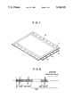
- FIG. 1is a perspective view showing a liquid crystal display in accordance with an embodiment of the present invention.
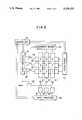
- FIG. 2is a schematic diagram showing a driving circuit of the liquid crystal display illustrated in FIG. 1.
- FIG. 3is a graphical diagram showing a scanning signal for displaying an image on the liquid crystal display.
- FIG. 4is a graphical diagram showing control signals given to FETS of the driving circuit.
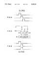
- FIG. 5is a schematic circuit diagram for explanation of the pressure detection by means of the liquid crystal display.
- FIG. 6is a graphical diagram showing an example of signals appearing when several points of the liquid crystal display are pushed.
- the displaycomprises a pair of glass substrates 1 and 2 between which a ferroelectric liquid crystal material is disposed.
- the substrate 1has a thickness of 0.5 mm and provides the front surface of the display.
- the substrate 2is made of a soda-lime glass pane of a thickness of 1.1 mm and constitutes the supporting structure of the display.
- the insides surface of the substrates 1 and 2are formed with parallel electrode strips constituting coloums and rows in a matrix arrangement respectively.
- the electrode stripsare formed by coating ITO films of 1300 ⁇ on the substrate followed by excimer laser patterning. Peripheral circuits are formed simultaneously as well as contact patterns for making connection with IC chips 4.
- the inner surface of the substrate 1is covered with a polyimide film of 200 angstroms thickness over the electrode strips.
- the polyimide filmis thermally annealed for 2 hours at 280° C. in order to be converted to an imide film and given rubbing treatment using a cloth which is characterized by a long soft pile.
- the inside surface of the other substrate 2is coated with a SiO 2 film of 150 angstroms thickness over the electrode and with an adhesive film pattern surrounding the pattern.
- the two substratesare joined under a pressure of 2 Kg/cm 2 at 180° C. for two hours. Then, a ferroelectric liquid crystal material is disposed between the substrates by vacuum injection. Finally, IC chips for signal processing are mounted on and connected with the peripheral circuit.
- FIG. 2is a schematic diagram showing the liquid crystal driving system.
- the row stripsare connected to a pulse generator 11 which supplies addressing pulsed signals as illustrated in FIG. 3.
- the column stripsare supplied with data signals from a segment driver 13 in order to display a visual image on the matrix. Each signal is generated by use of a shift register.
- One frameis constructed during each 1/30 second, i.e. there are 30 scanning cycles within one second. Out of the 30 cycles, the 30th cycle is alloted to a pressure detecting action.
- the addressing signal and the data signalare kept at a zero level during the 30th cycle as illustrated in FIG. 3.
- the row stripsare connected to the ground terminal through FETs 15 whose gates are supplied with control signals from a shift register 17.
- the column stripsare connected to one input terminals of AND gates 19 through operational amplifiers 21.
- the other input terminalsare connected to a high voltage source Vdd through a FET.
- the output terminals of the AND gates 19are coupled to the input terminals of a shift resister 25.
- the FETsare supplied with control signals as illustrated in FIG. 4 while the AND gates are enabled by inputtig a signal to the gate of the FET 23. By virtue of the control signals, the row strips are grounded successively.
- Numeral 27designates a control device which controls each element of the driving circuits for display and pressure
- FIG. 5a schematic diagram is illustrated showing an electric circuit which is realized if position A is pressed.
- the FET connected to the first rowis turned on during the first third of the detecting period.
- the shift registerreceives the data of the first row as (100) in synchronization with the turning on of the FET.
- the datais taken out from the shift register by shifing action.
- a signal timing chart of gate control signals input to the FETs and data input to the shift register when positions A, E and H are pushedis illustrated in FIG. 6.
Landscapes
- Engineering & Computer Science (AREA)
- General Engineering & Computer Science (AREA)
- Theoretical Computer Science (AREA)
- Physics & Mathematics (AREA)
- General Physics & Mathematics (AREA)
- Human Computer Interaction (AREA)
- Liquid Crystal Display Device Control (AREA)
- Liquid Crystal (AREA)
Abstract
Description
This Application is a continuation-in-part of application Ser. No. 150,150 filed Jan. 29, 1989, now U.S. Pat. No. 4,875,378.
The present invention relates to a liquid crystal display, and more particularly relates to a display device which is provided with a touch sensor.
There has been developed a liquid crystal display for use in lap-top personal computors or word-processors. For such liquid crystal displays, it will be convenient if the user can input information to the system through the display itself. This input method has already been available in case of CRTs. In the CRT of this type, a certain position is touched with a write pen whose tip is provided with a light sensor. In accordance with the timing of light reception at the tip, the touch position is detected. This structure, however, requires a somewhat complicated circuit increasing the production cost. Furthermore, this is not directly available for liquid crystal displays which utilize no scanning light.
It is therefore an object of the present invention to provide a liquid crystal display directly on which data inputting can be done.
In order to accomplish the above and other objects and advantages, a ferroelectric liquid crystal is used both as light influencing medium and as a pressure sensor. One cycle of scanning the display area is devoted to pressure detection for each several cycles of displaying frames.
This invention can be better understood from the following detailed description when read in conjunction with the drawing in which
FIG. 1 is a perspective view showing a liquid crystal display in accordance with an embodiment of the present invention.
FIG. 2 is a schematic diagram showing a driving circuit of the liquid crystal display illustrated in FIG. 1.
FIG. 3 is a graphical diagram showing a scanning signal for displaying an image on the liquid crystal display.
FIG. 4 is a graphical diagram showing control signals given to FETS of the driving circuit.
FIG. 5 is a schematic circuit diagram for explanation of the pressure detection by means of the liquid crystal display.
FIG. 6 is a graphical diagram showing an example of signals appearing when several points of the liquid crystal display are pushed.
Referring now to FIG. 1, a perspective view showing a bistable liquid crystal display is illustrated in accordance with an embodiment of the present invention. The display comprises a pair ofglass substrates substrate 1 has a thickness of 0.5 mm and provides the front surface of the display. Thesubstrate 2 is made of a soda-lime glass pane of a thickness of 1.1 mm and constitutes the supporting structure of the display. The insides surface of thesubstrates
The electrode strips are formed by coating ITO films of 1300 Å on the substrate followed by excimer laser patterning. Peripheral circuits are formed simultaneously as well as contact patterns for making connection with IC chips 4. The inner surface of thesubstrate 1 is covered with a polyimide film of 200 angstroms thickness over the electrode strips. The polyimide film is thermally annealed for 2 hours at 280° C. in order to be converted to an imide film and given rubbing treatment using a cloth which is characterized by a long soft pile. The inside surface of theother substrate 2 is coated with a SiO2 film of 150 angstroms thickness over the electrode and with an adhesive film pattern surrounding the pattern. After dusting the inside surface of thesubstrate 2 with spacers of 2.5 diameter SiO2 particles, the two substrates are joined under a pressure of 2 Kg/cm2 at 180° C. for two hours. Then, a ferroelectric liquid crystal material is disposed between the substrates by vacuum injection. Finally, IC chips for signal processing are mounted on and connected with the peripheral circuit.
Now, a driving method for the display will be explained. FIG. 2 is a schematic diagram showing the liquid crystal driving system. In the figure, only a 3×3 matrix display is illustrated for the purpose of clarity. In actual configurations, more large scale matrices may be employed. The row strips are connected to apulse generator 11 which supplies addressing pulsed signals as illustrated in FIG. 3. In synchronization with the addressing signals, the column strips are supplied with data signals from asegment driver 13 in order to display a visual image on the matrix. Each signal is generated by use of a shift register.
One frame is constructed during each 1/30 second, i.e. there are 30 scanning cycles within one second. Out of the 30 cycles, the 30th cycle is alloted to a pressure detecting action. The addressing signal and the data signal are kept at a zero level during the 30th cycle as illustrated in FIG. 3. The row strips are connected to the ground terminal throughFETs 15 whose gates are supplied with control signals from ashift register 17. The column strips are connected to one input terminals of ANDgates 19 throughoperational amplifiers 21. The other input terminals are connected to a high voltage source Vdd through a FET. The output terminals of the ANDgates 19 are coupled to the input terminals of ashift resister 25. During the 30th cycle, the FETs are supplied with control signals as illustrated in FIG. 4 while the AND gates are enabled by inputtig a signal to the gate of theFET 23. By virtue of the control signals, the row strips are grounded successively.Numeral 27 designates a control device which controls each element of the driving circuits for display and pressure detection.
When the liquid crystal layer between the substrate is pressed at a certain position, a voltage is generated across the liquid crystal layer at the position. In FIG. 5, a schematic diagram is illustrated showing an electric circuit which is realized if position A is pressed. The FET connected to the first row is turned on during the first third of the detecting period. The shift register receives the data of the first row as (100) in synchronization with the turning on of the FET. The data is taken out from the shift register by shifing action. A signal timing chart of gate control signals input to the FETs and data input to the shift register when positions A, E and H are pushed is illustrated in FIG. 6.
While several embodiments have been specifically described by way of examples, it is to be appreciated that the present invention is not limited to the particular examples described and that modifications and variations can be made without departing from the scope of the invention as defined by the appended claims.
Claims (11)
1. A liquid crystal display comprising:
a pair of substrates at least one of which is transparent;
an electrode arrangement formed on the inside surfaces of said substrates in order to define a plurality of pixels;
a liquid crystal material having a piezoelectric effect disposed between said substrates;
a means for supplying driving signals to said electrode arrangement in order to construct an image on said display;
a means for detecting the voltage generated across said liquid crystal material between said substrates due to pressure applied thereto; and
a means for controlling said driving means and detecting means in order that the displaying operation by means of said supplying means and the detection operation by means of said detecting means are performed alternately.
2. The display of claim 1 wherein said electrode arrangement comprises a plurality of first parallel conductive strips formed on one of said substrates and a plurality of second parallel conductive strips, said first and second strips being arranged orthgonally in order to form a matrix.
3. The display of claim 2 wherein said supplying means comprising an oscillator which supplies addressing signals to said first strips and a driver which supplies input signals to said second strips in synchronization with said addressing signals.
4. The display of claim 3 wherein said detecting means comprises a switching circuit which sequentially grounds one of said first strips whereas the others of said first strips are opened, and a shift register which stores the voltage levels of said second strips in synchronization with said switching circuit.
5. The display of claim 1 wherein the pressure detection operation scanning through the display area is effected after the display operation of several frames.
6. The display of claim 1 wherein said electrode arrangement is scanned with said driving signals n times (where n>2) and subsequently scanned with voltage detection signals one time.
7. The display of claim 1 wherein said liquid crystal material comprises a ferroelectric liquid crystal.
8. A method for operating a liquid crystal display device comprising a pair of substrates with a gap therebetween filled with a liquid crystal layer having a piezoelectric effect and an electrode arrangement defining a plurality of picture elements in said liquid crystal layer, said method comprising the steps of:
first scanning said picture elements with signals for displaying a visual image in said device;
second scanning said picture elements with signals subsequent to said first scanning for sensing a voltage generated by said liquid crystal layer at each picture element in response to a pressure applied thereto; and
repeating said first and second scanning steps.
9. The method of claim 8 wherein said liquid crystal layer comprises a ferroelectric liquid crystal layer.
10. A liquid crystal device comprising:
a pair of substrates, at least one of which is transparent, each having an inside and an outside;
row and column electrode strips respectively formed on the insides of said substrates;
a liquid crystal layer having a piezoelectric effect disposed between said substrates;
means for scanning said row electrode strips with address signals;
means for supplying said column electrode strips with data signals in synchronization with said address signals;
means for detecting a voltage generated across said liquid crystal layer in response to a pressure applied thereto, said means comprising a means for scanning said row electrode strips with ground level signals, a plurality of AND gates where each of said column electrode strips is connected to one of two inputs of said AND gates respectively, a means for applying a voltage to the other one of said two inputs of said AND gates and a means for detecting outputs of said AND gates; and
a controller for driving said means for scanning said row electrode strips, said means for supplying said column electrode strips and said means for detecting a voltage in order that a display operation and a pressure detection of said liquid crystal device are performed alternatively.
11. The device of claim 10 wherein said liquid crystal layer comprises a ferroelectric liquid crystal.
Priority Applications (1)
| Application Number | Priority Date | Filing Date | Title |
|---|---|---|---|
| US07/361,954US5159323A (en) | 1987-02-19 | 1989-06-06 | Liquid crystal display |
Applications Claiming Priority (4)
| Application Number | Priority Date | Filing Date | Title |
|---|---|---|---|
| JP62037566AJPS63204313A (en) | 1987-02-19 | 1987-02-19 | Pressure sensor |
| JP63-143331 | 1988-06-09 | ||
| JP63143331AJPH021891A (en) | 1988-06-09 | 1988-06-09 | Liquid crystal display device |
| US07/361,954US5159323A (en) | 1987-02-19 | 1989-06-06 | Liquid crystal display |
Related Parent Applications (1)
| Application Number | Title | Priority Date | Filing Date |
|---|---|---|---|
| US07150150Continuation-In-Part | 1989-01-29 |
Publications (1)
| Publication Number | Publication Date |
|---|---|
| US5159323Atrue US5159323A (en) | 1992-10-27 |
Family
ID=27289508
Family Applications (1)
| Application Number | Title | Priority Date | Filing Date |
|---|---|---|---|
| US07/361,954Expired - Fee RelatedUS5159323A (en) | 1987-02-19 | 1989-06-06 | Liquid crystal display |
Country Status (1)
| Country | Link |
|---|---|
| US (1) | US5159323A (en) |
Cited By (35)
| Publication number | Priority date | Publication date | Assignee | Title |
|---|---|---|---|---|
| EP0618527A1 (en)* | 1993-03-29 | 1994-10-05 | NCR International, Inc. | Input means for liquid crystal display |
| US5392058A (en)* | 1991-05-15 | 1995-02-21 | Sharp Kabushiki Kaisha | Display-integrated type tablet device |
| US5418551A (en)* | 1988-12-19 | 1995-05-23 | Sharp Kabushiki Kaisha | Tablet integrated with display |
| WO1995019030A1 (en)* | 1994-01-05 | 1995-07-13 | Pois, Inc. | Apparatus and method for a personal onboard information system |
| US5528267A (en)* | 1988-12-19 | 1996-06-18 | Sharp Kabushiki Kaisha | Tablet integrated with display |
| US5610629A (en)* | 1991-12-06 | 1997-03-11 | Ncr Corporation | Pen input to liquid crystal display |
| US5673041A (en)* | 1994-03-30 | 1997-09-30 | Chatigny; Joseph Victor | Reflective mode ultrasonic touch sensitive switch |
| US5847690A (en)* | 1995-10-24 | 1998-12-08 | Lucent Technologies Inc. | Integrated liquid crystal display and digitizer having a black matrix layer adapted for sensing screen touch location |
| US5984874A (en)* | 1997-08-14 | 1999-11-16 | Southwest Research Institute | Pressure and temperature sensor transducer array |
| US20030006972A1 (en)* | 1999-07-31 | 2003-01-09 | Blanchard Randall D. | Touch panel with improved optical performance |
| US6664950B1 (en) | 1999-11-17 | 2003-12-16 | L-3 Communications | Resistive touch panel using removable, tensioned top layer |
| US20040004605A1 (en)* | 2002-06-25 | 2004-01-08 | David Albert M. | Laminated touch screen |
| US6677934B1 (en) | 1999-07-30 | 2004-01-13 | L-3 Communications | Infrared touch panel with improved sunlight rejection |
| WO2003079176A3 (en)* | 2002-03-15 | 2004-02-05 | Koninkl Philips Electronics Nv | Touch sensitive display device |
| DE10241523A1 (en)* | 2002-09-07 | 2004-03-11 | Bts Media Solutions Gmbh | Combined display and input panel for a video mixer system has a display and input panel separated by a sensor foil |
| WO2004001662A3 (en)* | 2002-06-25 | 2004-03-25 | 3M Innovative Properties Co | Touch sensor |
| WO2004053909A1 (en)* | 2002-12-09 | 2004-06-24 | Koninklijke Philips Electronics N.V. | Transparent touch-sensitive switching system |
| US20040155991A1 (en)* | 2002-11-21 | 2004-08-12 | Lowles Robert J. | System and method of integrating a touchscreen within an LCD |
| WO2004023440A3 (en)* | 2002-09-06 | 2004-11-04 | Koninkl Philips Electronics Nv | Touch sensing display |
| WO2005015373A3 (en)* | 2003-08-11 | 2006-03-23 | Koninkl Philips Electronics Nv | A touch sensitive display |
| US7042433B1 (en)* | 1999-05-14 | 2006-05-09 | Sharp Kabushiki Kaisha | Signal line driving circuit and image display device |
| US20060138983A1 (en)* | 2004-12-23 | 2006-06-29 | Samsung Electronics Co., Ltd. | Display device and driving apparatus thereof |
| WO2007029075A1 (en)* | 2005-09-08 | 2007-03-15 | Nokia Corporation | Multipurpose programmable adjustable keyboard (mpak) |
| US20070290963A1 (en)* | 2006-06-14 | 2007-12-20 | Hannstar Display Corp. | Image sensor array and liquid crystal display with sensor elements |
| CN101625488B (en)* | 2008-07-09 | 2011-09-28 | 瀚宇彩晶股份有限公司 | Display device and method for driving display panel thereof |
| US20120075226A1 (en)* | 2009-06-11 | 2012-03-29 | Murata Manufacturing Co., Ltd. | Touch Panel and Touch Type Input Device |
| US20120127136A1 (en)* | 2010-08-18 | 2012-05-24 | Kent Displays Incorporated | Display device including piezoelectric and liquid crystal layers |
| WO2014037016A1 (en)* | 2012-09-04 | 2014-03-13 | Joanneum Research Forschungsgesellschaft Mbh | Printed piezoelectric pressure sensing foil |
| US9501167B2 (en) | 2014-10-22 | 2016-11-22 | Synaptics Incorporated | Scanned piezoelectric touch sensor device |
| CN106197769A (en)* | 2016-08-12 | 2016-12-07 | 京东方科技集团股份有限公司 | Excess pressure monitoring device, method and polaroid attaching device |
| US20170010746A1 (en)* | 2004-05-06 | 2017-01-12 | Apple Inc. | Multipoint touchscreen |
| EP2469380A3 (en)* | 2010-12-22 | 2017-07-19 | Apple Inc. | Integrated touch screens |
| US10191576B2 (en) | 2006-06-09 | 2019-01-29 | Apple Inc. | Touch screen liquid crystal display |
| US10521065B2 (en) | 2007-01-05 | 2019-12-31 | Apple Inc. | Touch screen stack-ups |
| WO2020194135A1 (en)* | 2019-03-22 | 2020-10-01 | Gentex Corporation | Piezoelectric films with low haze and methods of making and using |
Citations (4)
| Publication number | Priority date | Publication date | Assignee | Title |
|---|---|---|---|---|
| US4363029A (en)* | 1980-11-17 | 1982-12-07 | Texas Instruments Incorporated | Switch for sensing proximity of an operator |
| US4529968A (en)* | 1981-11-16 | 1985-07-16 | The Secretary Of State For Defence In Her Britannic Majesty's Government Of The United Kingdom Of Great Britain And Northern Ireland | Touch sensitive liquid crystal switch |
| US4839634A (en)* | 1986-12-01 | 1989-06-13 | More Edward S | Electro-optic slate for input/output of hand-entered textual and graphic information |
| US4875378A (en)* | 1987-02-19 | 1989-10-24 | Semiconductor Energy Laboratory Co., Ltd. | Pressure sensor with a ferroelectric liquid crystal layer |
- 1989
- 1989-06-06USUS07/361,954patent/US5159323A/ennot_activeExpired - Fee Related
Patent Citations (4)
| Publication number | Priority date | Publication date | Assignee | Title |
|---|---|---|---|---|
| US4363029A (en)* | 1980-11-17 | 1982-12-07 | Texas Instruments Incorporated | Switch for sensing proximity of an operator |
| US4529968A (en)* | 1981-11-16 | 1985-07-16 | The Secretary Of State For Defence In Her Britannic Majesty's Government Of The United Kingdom Of Great Britain And Northern Ireland | Touch sensitive liquid crystal switch |
| US4839634A (en)* | 1986-12-01 | 1989-06-13 | More Edward S | Electro-optic slate for input/output of hand-entered textual and graphic information |
| US4875378A (en)* | 1987-02-19 | 1989-10-24 | Semiconductor Energy Laboratory Co., Ltd. | Pressure sensor with a ferroelectric liquid crystal layer |
Cited By (73)
| Publication number | Priority date | Publication date | Assignee | Title |
|---|---|---|---|---|
| US5418551A (en)* | 1988-12-19 | 1995-05-23 | Sharp Kabushiki Kaisha | Tablet integrated with display |
| US5528267A (en)* | 1988-12-19 | 1996-06-18 | Sharp Kabushiki Kaisha | Tablet integrated with display |
| US5392058A (en)* | 1991-05-15 | 1995-02-21 | Sharp Kabushiki Kaisha | Display-integrated type tablet device |
| US5610629A (en)* | 1991-12-06 | 1997-03-11 | Ncr Corporation | Pen input to liquid crystal display |
| EP0618527A1 (en)* | 1993-03-29 | 1994-10-05 | NCR International, Inc. | Input means for liquid crystal display |
| US5859628A (en)* | 1994-01-05 | 1999-01-12 | Pois, Inc. | Apparatus and method for a personal onboard information system |
| WO1995019030A1 (en)* | 1994-01-05 | 1995-07-13 | Pois, Inc. | Apparatus and method for a personal onboard information system |
| US5673041A (en)* | 1994-03-30 | 1997-09-30 | Chatigny; Joseph Victor | Reflective mode ultrasonic touch sensitive switch |
| US5847690A (en)* | 1995-10-24 | 1998-12-08 | Lucent Technologies Inc. | Integrated liquid crystal display and digitizer having a black matrix layer adapted for sensing screen touch location |
| US5984874A (en)* | 1997-08-14 | 1999-11-16 | Southwest Research Institute | Pressure and temperature sensor transducer array |
| US7042433B1 (en)* | 1999-05-14 | 2006-05-09 | Sharp Kabushiki Kaisha | Signal line driving circuit and image display device |
| US6677934B1 (en) | 1999-07-30 | 2004-01-13 | L-3 Communications | Infrared touch panel with improved sunlight rejection |
| US6512512B1 (en) | 1999-07-31 | 2003-01-28 | Litton Systems, Inc. | Touch panel with improved optical performance |
| US20030006971A1 (en)* | 1999-07-31 | 2003-01-09 | Blanchard Randall D. | Touch panel with improved optical performance |
| US20030006972A1 (en)* | 1999-07-31 | 2003-01-09 | Blanchard Randall D. | Touch panel with improved optical performance |
| US6664950B1 (en) | 1999-11-17 | 2003-12-16 | L-3 Communications | Resistive touch panel using removable, tensioned top layer |
| US7071927B2 (en) | 1999-11-17 | 2006-07-04 | L-3 Communications Corporation | Resistive touch panel using removable, tensioned top layer |
| US20040095332A1 (en)* | 1999-11-17 | 2004-05-20 | Blanchard Randall D. | Resistive touch panel using removable, tensioned top layer |
| WO2003079176A3 (en)* | 2002-03-15 | 2004-02-05 | Koninkl Philips Electronics Nv | Touch sensitive display device |
| US7819998B2 (en) | 2002-06-25 | 2010-10-26 | David Albert M | Method of forming a touch screen laminate |
| US8760433B2 (en) | 2002-06-25 | 2014-06-24 | Albert M David | Laminated touch screen |
| US7345680B2 (en) | 2002-06-25 | 2008-03-18 | David Albert M | Laminated touch screen |
| US20040004605A1 (en)* | 2002-06-25 | 2004-01-08 | David Albert M. | Laminated touch screen |
| US20110032205A1 (en)* | 2002-06-25 | 2011-02-10 | David Albert M | Laminated Touch Screen |
| US20080173395A1 (en)* | 2002-06-25 | 2008-07-24 | David Albert M | Method of forming a touch screen laminate |
| WO2004001662A3 (en)* | 2002-06-25 | 2004-03-25 | 3M Innovative Properties Co | Touch sensor |
| WO2004023440A3 (en)* | 2002-09-06 | 2004-11-04 | Koninkl Philips Electronics Nv | Touch sensing display |
| DE10241523A1 (en)* | 2002-09-07 | 2004-03-11 | Bts Media Solutions Gmbh | Combined display and input panel for a video mixer system has a display and input panel separated by a sensor foil |
| WO2004046905A3 (en)* | 2002-11-21 | 2004-08-26 | Research In Motion Ltd | Device and method of integrating a touchscreen within an liquid crystal display |
| US20080030479A1 (en)* | 2002-11-21 | 2008-02-07 | Research In Motion Limited | System and method of integrating a touchscreen within an lcd |
| US20040155991A1 (en)* | 2002-11-21 | 2004-08-12 | Lowles Robert J. | System and method of integrating a touchscreen within an LCD |
| US7388571B2 (en) | 2002-11-21 | 2008-06-17 | Research In Motion Limited | System and method of integrating a touchscreen within an LCD |
| US20060071819A1 (en)* | 2002-12-09 | 2006-04-06 | Johnson Mark T | Transparent touch-sensitive switching system |
| WO2004053909A1 (en)* | 2002-12-09 | 2004-06-24 | Koninklijke Philips Electronics N.V. | Transparent touch-sensitive switching system |
| WO2005015373A3 (en)* | 2003-08-11 | 2006-03-23 | Koninkl Philips Electronics Nv | A touch sensitive display |
| US11604547B2 (en) | 2004-05-06 | 2023-03-14 | Apple Inc. | Multipoint touchscreen |
| US20170010746A1 (en)* | 2004-05-06 | 2017-01-12 | Apple Inc. | Multipoint touchscreen |
| US10331259B2 (en)* | 2004-05-06 | 2019-06-25 | Apple Inc. | Multipoint touchscreen |
| US10908729B2 (en) | 2004-05-06 | 2021-02-02 | Apple Inc. | Multipoint touchscreen |
| US20060138983A1 (en)* | 2004-12-23 | 2006-06-29 | Samsung Electronics Co., Ltd. | Display device and driving apparatus thereof |
| US7973777B2 (en) | 2004-12-23 | 2011-07-05 | Samsung Electronics Co., Ltd. | Display device and driving apparatus including a photo sensing circuit and a pressure sensing circuit and method thereof |
| WO2007029075A1 (en)* | 2005-09-08 | 2007-03-15 | Nokia Corporation | Multipurpose programmable adjustable keyboard (mpak) |
| EP1934689A4 (en)* | 2005-09-08 | 2012-07-04 | Nokia Corp | MULTIFUNCTIONAL PROGRAMMABLE ADJUSTABLE KEYBOARD (MPAK) |
| US20070097595A1 (en)* | 2005-09-08 | 2007-05-03 | Nokia Corporation | Multipurpose programmable adjustable keyboard (MPAK) |
| US11175762B2 (en) | 2006-06-09 | 2021-11-16 | Apple Inc. | Touch screen liquid crystal display |
| US10976846B2 (en) | 2006-06-09 | 2021-04-13 | Apple Inc. | Touch screen liquid crystal display |
| US11886651B2 (en) | 2006-06-09 | 2024-01-30 | Apple Inc. | Touch screen liquid crystal display |
| US10191576B2 (en) | 2006-06-09 | 2019-01-29 | Apple Inc. | Touch screen liquid crystal display |
| US20070290963A1 (en)* | 2006-06-14 | 2007-12-20 | Hannstar Display Corp. | Image sensor array and liquid crystal display with sensor elements |
| US10521065B2 (en) | 2007-01-05 | 2019-12-31 | Apple Inc. | Touch screen stack-ups |
| CN101625488B (en)* | 2008-07-09 | 2011-09-28 | 瀚宇彩晶股份有限公司 | Display device and method for driving display panel thereof |
| US10146392B2 (en) | 2009-06-11 | 2018-12-04 | Murata Manufacturing Co., Ltd. | Touch panel and touch type input device |
| US20130328817A1 (en)* | 2009-06-11 | 2013-12-12 | Murata Manufacturing Co. | Touch Panel and Touch Type Input Device |
| US9128553B2 (en)* | 2009-06-11 | 2015-09-08 | Murata Manufacturing Co., Ltd. | Touch panel and touch type input device |
| US9134826B2 (en)* | 2009-06-11 | 2015-09-15 | Murata Maufacturing Co., Ltd. | Touch panel and touch type input device |
| US9804725B2 (en) | 2009-06-11 | 2017-10-31 | Murata Manufacturing Co., Ltd. | Touch panel and touch type input device |
| US20120075226A1 (en)* | 2009-06-11 | 2012-03-29 | Murata Manufacturing Co., Ltd. | Touch Panel and Touch Type Input Device |
| US20120127136A1 (en)* | 2010-08-18 | 2012-05-24 | Kent Displays Incorporated | Display device including piezoelectric and liquid crystal layers |
| US9727193B2 (en) | 2010-12-22 | 2017-08-08 | Apple Inc. | Integrated touch screens |
| EP2469380A3 (en)* | 2010-12-22 | 2017-07-19 | Apple Inc. | Integrated touch screens |
| US10409434B2 (en) | 2010-12-22 | 2019-09-10 | Apple Inc. | Integrated touch screens |
| CN104813260B (en)* | 2012-09-04 | 2018-02-13 | 约阿内研究有限责任公司 | Print piezoelectric pressure sensing paper tinsel |
| KR20150047506A (en)* | 2012-09-04 | 2015-05-04 | 요하노이움 리서치 포르슝스게젤샤프트 엠베하 | Printed piezoelectric pressure sensing foil |
| US9612690B2 (en) | 2012-09-04 | 2017-04-04 | Fh-Oö Forschungs And Entwicklungs Gmbh | Printed piezoelectric pressure sensing foil |
| CN104813260A (en)* | 2012-09-04 | 2015-07-29 | 约阿内研究有限责任公司 | Printed piezoelectric pressure sensing foil |
| EP3702894A1 (en)* | 2012-09-04 | 2020-09-02 | JOANNEUM RESEARCH Forschungsgesellschaft mbH | Printed piezoelectric pressure sensing foil |
| WO2014037016A1 (en)* | 2012-09-04 | 2014-03-13 | Joanneum Research Forschungsgesellschaft Mbh | Printed piezoelectric pressure sensing foil |
| US9857913B2 (en) | 2014-10-22 | 2018-01-02 | Synaptics Incorporated | Scanned piezoelectric touch sensor device |
| US9501167B2 (en) | 2014-10-22 | 2016-11-22 | Synaptics Incorporated | Scanned piezoelectric touch sensor device |
| CN106197769B (en)* | 2016-08-12 | 2019-08-09 | 京东方科技集团股份有限公司 | Overpressure monitoring device, method and polarizer attaching equipment |
| CN106197769A (en)* | 2016-08-12 | 2016-12-07 | 京东方科技集团股份有限公司 | Excess pressure monitoring device, method and polaroid attaching device |
| WO2020194135A1 (en)* | 2019-03-22 | 2020-10-01 | Gentex Corporation | Piezoelectric films with low haze and methods of making and using |
| US11531414B2 (en) | 2019-03-22 | 2022-12-20 | Gentex Corporation | Piezoelectric films with low haze and methods of making and using |
Similar Documents
| Publication | Publication Date | Title |
|---|---|---|
| US5159323A (en) | Liquid crystal display | |
| JP3188498B2 (en) | Active matrix liquid crystal display device | |
| JP4920245B2 (en) | Liquid crystal display with a sensing element | |
| EP0464908B1 (en) | Touch sensor array systems and display systems | |
| JP5281783B2 (en) | Display device and driving method thereof | |
| US20170045975A1 (en) | Display device and method of driving the same | |
| JPH1124041A (en) | Liquid crystal display | |
| JPH05297403A (en) | Liquid crystal display enabling pen input | |
| US5528267A (en) | Tablet integrated with display | |
| US5181131A (en) | Power conserving driver circuit for liquid crystal displays | |
| TWI280559B (en) | Flat-panel display device | |
| JPH0225834A (en) | Liquid crystal device | |
| JPH07109455B2 (en) | Driving method for electro-optical device | |
| JP3329028B2 (en) | Display device with coordinate detection device | |
| TWI736267B (en) | Driving method and display device | |
| JP2000330518A (en) | Active matrix type liquid crystal display | |
| JPH04337824A (en) | integrated display tablet | |
| CN115390698A (en) | Touch peep-proof screen and control method | |
| JP2003099018A (en) | Flat panel display | |
| JPH03294919A (en) | Display device with tablet function | |
| JPH03296127A (en) | Flat display with tablet function | |
| JP3350083B2 (en) | Coordinate detection device | |
| JPH028814A (en) | liquid crystal device | |
| JPH09292598A (en) | Liquid crystal distal device provided with input function | |
| JP3183773B2 (en) | Display integrated tablet device |
Legal Events
| Date | Code | Title | Description |
|---|---|---|---|
| AS | Assignment | Owner name:SEMICONDUCTOR ENERGY LABORATORY CO., LTD., 398, HA Free format text:ASSIGNMENT OF ASSIGNORS INTEREST.;ASSIGNORS:MASE, AKIRA;YAMAZAKI, SHUNPEI;REEL/FRAME:005088/0058;SIGNING DATES FROM 19890529 TO 19890530 | |
| FEPP | Fee payment procedure | Free format text:PAYOR NUMBER ASSIGNED (ORIGINAL EVENT CODE: ASPN); ENTITY STATUS OF PATENT OWNER: LARGE ENTITY | |
| FPAY | Fee payment | Year of fee payment:4 | |
| FPAY | Fee payment | Year of fee payment:8 | |
| REMI | Maintenance fee reminder mailed | ||
| LAPS | Lapse for failure to pay maintenance fees | ||
| STCH | Information on status: patent discontinuation | Free format text:PATENT EXPIRED DUE TO NONPAYMENT OF MAINTENANCE FEES UNDER 37 CFR 1.362 | |
| FP | Lapsed due to failure to pay maintenance fee | Effective date:20041027 |