US5156881A - Method for forming a film on a substrate by activating a reactive gas - Google Patents
Method for forming a film on a substrate by activating a reactive gasDownload PDFInfo
- Publication number
- US5156881A US5156881AUS07/686,283US68628391AUS5156881AUS 5156881 AUS5156881 AUS 5156881AUS 68628391 AUS68628391 AUS 68628391AUS 5156881 AUS5156881 AUS 5156881A
- Authority
- US
- United States
- Prior art keywords
- thin film
- film forming
- forming method
- reactive gas
- substrate
- Prior art date
- Legal status (The legal status is an assumption and is not a legal conclusion. Google has not performed a legal analysis and makes no representation as to the accuracy of the status listed.)
- Expired - Lifetime
Links
Images


Classifications
- H—ELECTRICITY
- H01—ELECTRIC ELEMENTS
- H01L—SEMICONDUCTOR DEVICES NOT COVERED BY CLASS H10
- H01L21/00—Processes or apparatus adapted for the manufacture or treatment of semiconductor or solid state devices or of parts thereof
- H01L21/02—Manufacture or treatment of semiconductor devices or of parts thereof
- H01L21/04—Manufacture or treatment of semiconductor devices or of parts thereof the devices having potential barriers, e.g. a PN junction, depletion layer or carrier concentration layer
- H01L21/18—Manufacture or treatment of semiconductor devices or of parts thereof the devices having potential barriers, e.g. a PN junction, depletion layer or carrier concentration layer the devices having semiconductor bodies comprising elements of Group IV of the Periodic Table or AIIIBV compounds with or without impurities, e.g. doping materials
- H01L21/30—Treatment of semiconductor bodies using processes or apparatus not provided for in groups H01L21/20 - H01L21/26
- H01L21/31—Treatment of semiconductor bodies using processes or apparatus not provided for in groups H01L21/20 - H01L21/26 to form insulating layers thereon, e.g. for masking or by using photolithographic techniques; After treatment of these layers; Selection of materials for these layers
- H—ELECTRICITY
- H01—ELECTRIC ELEMENTS
- H01L—SEMICONDUCTOR DEVICES NOT COVERED BY CLASS H10
- H01L21/00—Processes or apparatus adapted for the manufacture or treatment of semiconductor or solid state devices or of parts thereof
- H01L21/02—Manufacture or treatment of semiconductor devices or of parts thereof
- H01L21/02104—Forming layers
- H01L21/02107—Forming insulating materials on a substrate
- H01L21/02225—Forming insulating materials on a substrate characterised by the process for the formation of the insulating layer
- H01L21/0226—Forming insulating materials on a substrate characterised by the process for the formation of the insulating layer formation by a deposition process
- H01L21/02263—Forming insulating materials on a substrate characterised by the process for the formation of the insulating layer formation by a deposition process deposition from the gas or vapour phase
- H01L21/02271—Forming insulating materials on a substrate characterised by the process for the formation of the insulating layer formation by a deposition process deposition from the gas or vapour phase deposition by decomposition or reaction of gaseous or vapour phase compounds, i.e. chemical vapour deposition
- H01L21/02274—Forming insulating materials on a substrate characterised by the process for the formation of the insulating layer formation by a deposition process deposition from the gas or vapour phase deposition by decomposition or reaction of gaseous or vapour phase compounds, i.e. chemical vapour deposition in the presence of a plasma [PECVD]
- C—CHEMISTRY; METALLURGY
- C23—COATING METALLIC MATERIAL; COATING MATERIAL WITH METALLIC MATERIAL; CHEMICAL SURFACE TREATMENT; DIFFUSION TREATMENT OF METALLIC MATERIAL; COATING BY VACUUM EVAPORATION, BY SPUTTERING, BY ION IMPLANTATION OR BY CHEMICAL VAPOUR DEPOSITION, IN GENERAL; INHIBITING CORROSION OF METALLIC MATERIAL OR INCRUSTATION IN GENERAL
- C23C—COATING METALLIC MATERIAL; COATING MATERIAL WITH METALLIC MATERIAL; SURFACE TREATMENT OF METALLIC MATERIAL BY DIFFUSION INTO THE SURFACE, BY CHEMICAL CONVERSION OR SUBSTITUTION; COATING BY VACUUM EVAPORATION, BY SPUTTERING, BY ION IMPLANTATION OR BY CHEMICAL VAPOUR DEPOSITION, IN GENERAL
- C23C16/00—Chemical coating by decomposition of gaseous compounds, without leaving reaction products of surface material in the coating, i.e. chemical vapour deposition [CVD] processes
- C23C16/04—Coating on selected surface areas, e.g. using masks
- C23C16/045—Coating cavities or hollow spaces, e.g. interior of tubes; Infiltration of porous substrates
- C—CHEMISTRY; METALLURGY
- C23—COATING METALLIC MATERIAL; COATING MATERIAL WITH METALLIC MATERIAL; CHEMICAL SURFACE TREATMENT; DIFFUSION TREATMENT OF METALLIC MATERIAL; COATING BY VACUUM EVAPORATION, BY SPUTTERING, BY ION IMPLANTATION OR BY CHEMICAL VAPOUR DEPOSITION, IN GENERAL; INHIBITING CORROSION OF METALLIC MATERIAL OR INCRUSTATION IN GENERAL
- C23C—COATING METALLIC MATERIAL; COATING MATERIAL WITH METALLIC MATERIAL; SURFACE TREATMENT OF METALLIC MATERIAL BY DIFFUSION INTO THE SURFACE, BY CHEMICAL CONVERSION OR SUBSTITUTION; COATING BY VACUUM EVAPORATION, BY SPUTTERING, BY ION IMPLANTATION OR BY CHEMICAL VAPOUR DEPOSITION, IN GENERAL
- C23C16/00—Chemical coating by decomposition of gaseous compounds, without leaving reaction products of surface material in the coating, i.e. chemical vapour deposition [CVD] processes
- C23C16/22—Chemical coating by decomposition of gaseous compounds, without leaving reaction products of surface material in the coating, i.e. chemical vapour deposition [CVD] processes characterised by the deposition of inorganic material, other than metallic material
- C23C16/30—Deposition of compounds, mixtures or solid solutions, e.g. borides, carbides, nitrides
- C23C16/40—Oxides
- C23C16/401—Oxides containing silicon
- C23C16/402—Silicon dioxide
- C—CHEMISTRY; METALLURGY
- C23—COATING METALLIC MATERIAL; COATING MATERIAL WITH METALLIC MATERIAL; CHEMICAL SURFACE TREATMENT; DIFFUSION TREATMENT OF METALLIC MATERIAL; COATING BY VACUUM EVAPORATION, BY SPUTTERING, BY ION IMPLANTATION OR BY CHEMICAL VAPOUR DEPOSITION, IN GENERAL; INHIBITING CORROSION OF METALLIC MATERIAL OR INCRUSTATION IN GENERAL
- C23C—COATING METALLIC MATERIAL; COATING MATERIAL WITH METALLIC MATERIAL; SURFACE TREATMENT OF METALLIC MATERIAL BY DIFFUSION INTO THE SURFACE, BY CHEMICAL CONVERSION OR SUBSTITUTION; COATING BY VACUUM EVAPORATION, BY SPUTTERING, BY ION IMPLANTATION OR BY CHEMICAL VAPOUR DEPOSITION, IN GENERAL
- C23C16/00—Chemical coating by decomposition of gaseous compounds, without leaving reaction products of surface material in the coating, i.e. chemical vapour deposition [CVD] processes
- C23C16/44—Chemical coating by decomposition of gaseous compounds, without leaving reaction products of surface material in the coating, i.e. chemical vapour deposition [CVD] processes characterised by the method of coating
- C23C16/46—Chemical coating by decomposition of gaseous compounds, without leaving reaction products of surface material in the coating, i.e. chemical vapour deposition [CVD] processes characterised by the method of coating characterised by the method used for heating the substrate
- H—ELECTRICITY
- H01—ELECTRIC ELEMENTS
- H01L—SEMICONDUCTOR DEVICES NOT COVERED BY CLASS H10
- H01L21/00—Processes or apparatus adapted for the manufacture or treatment of semiconductor or solid state devices or of parts thereof
- H01L21/02—Manufacture or treatment of semiconductor devices or of parts thereof
- H01L21/02104—Forming layers
- H01L21/02107—Forming insulating materials on a substrate
- H01L21/02109—Forming insulating materials on a substrate characterised by the type of layer, e.g. type of material, porous/non-porous, pre-cursors, mixtures or laminates
- H01L21/02112—Forming insulating materials on a substrate characterised by the type of layer, e.g. type of material, porous/non-porous, pre-cursors, mixtures or laminates characterised by the material of the layer
- H01L21/02123—Forming insulating materials on a substrate characterised by the type of layer, e.g. type of material, porous/non-porous, pre-cursors, mixtures or laminates characterised by the material of the layer the material containing silicon
- H01L21/02126—Forming insulating materials on a substrate characterised by the type of layer, e.g. type of material, porous/non-porous, pre-cursors, mixtures or laminates characterised by the material of the layer the material containing silicon the material containing Si, O, and at least one of H, N, C, F, or other non-metal elements, e.g. SiOC, SiOC:H or SiONC
- H01L21/02129—Forming insulating materials on a substrate characterised by the type of layer, e.g. type of material, porous/non-porous, pre-cursors, mixtures or laminates characterised by the material of the layer the material containing silicon the material containing Si, O, and at least one of H, N, C, F, or other non-metal elements, e.g. SiOC, SiOC:H or SiONC the material being boron or phosphorus doped silicon oxides, e.g. BPSG, BSG or PSG
- H—ELECTRICITY
- H01—ELECTRIC ELEMENTS
- H01L—SEMICONDUCTOR DEVICES NOT COVERED BY CLASS H10
- H01L21/00—Processes or apparatus adapted for the manufacture or treatment of semiconductor or solid state devices or of parts thereof
- H01L21/02—Manufacture or treatment of semiconductor devices or of parts thereof
- H01L21/02104—Forming layers
- H01L21/02107—Forming insulating materials on a substrate
- H01L21/02109—Forming insulating materials on a substrate characterised by the type of layer, e.g. type of material, porous/non-porous, pre-cursors, mixtures or laminates
- H01L21/02112—Forming insulating materials on a substrate characterised by the type of layer, e.g. type of material, porous/non-porous, pre-cursors, mixtures or laminates characterised by the material of the layer
- H01L21/02123—Forming insulating materials on a substrate characterised by the type of layer, e.g. type of material, porous/non-porous, pre-cursors, mixtures or laminates characterised by the material of the layer the material containing silicon
- H01L21/0217—Forming insulating materials on a substrate characterised by the type of layer, e.g. type of material, porous/non-porous, pre-cursors, mixtures or laminates characterised by the material of the layer the material containing silicon the material being a silicon nitride not containing oxygen, e.g. SixNy or SixByNz
- H—ELECTRICITY
- H01—ELECTRIC ELEMENTS
- H01L—SEMICONDUCTOR DEVICES NOT COVERED BY CLASS H10
- H01L21/00—Processes or apparatus adapted for the manufacture or treatment of semiconductor or solid state devices or of parts thereof
- H01L21/02—Manufacture or treatment of semiconductor devices or of parts thereof
- H01L21/02104—Forming layers
- H01L21/02107—Forming insulating materials on a substrate
- H01L21/02109—Forming insulating materials on a substrate characterised by the type of layer, e.g. type of material, porous/non-porous, pre-cursors, mixtures or laminates
- H01L21/02205—Forming insulating materials on a substrate characterised by the type of layer, e.g. type of material, porous/non-porous, pre-cursors, mixtures or laminates the layer being characterised by the precursor material for deposition
- H01L21/02208—Forming insulating materials on a substrate characterised by the type of layer, e.g. type of material, porous/non-porous, pre-cursors, mixtures or laminates the layer being characterised by the precursor material for deposition the precursor containing a compound comprising Si
- H01L21/02211—Forming insulating materials on a substrate characterised by the type of layer, e.g. type of material, porous/non-porous, pre-cursors, mixtures or laminates the layer being characterised by the precursor material for deposition the precursor containing a compound comprising Si the compound being a silane, e.g. disilane, methylsilane or chlorosilane
- H—ELECTRICITY
- H01—ELECTRIC ELEMENTS
- H01L—SEMICONDUCTOR DEVICES NOT COVERED BY CLASS H10
- H01L21/00—Processes or apparatus adapted for the manufacture or treatment of semiconductor or solid state devices or of parts thereof
- H01L21/02—Manufacture or treatment of semiconductor devices or of parts thereof
- H01L21/02104—Forming layers
- H01L21/02107—Forming insulating materials on a substrate
- H01L21/02225—Forming insulating materials on a substrate characterised by the process for the formation of the insulating layer
- H01L21/0226—Forming insulating materials on a substrate characterised by the process for the formation of the insulating layer formation by a deposition process
- H01L21/02263—Forming insulating materials on a substrate characterised by the process for the formation of the insulating layer formation by a deposition process deposition from the gas or vapour phase
- H01L21/02271—Forming insulating materials on a substrate characterised by the process for the formation of the insulating layer formation by a deposition process deposition from the gas or vapour phase deposition by decomposition or reaction of gaseous or vapour phase compounds, i.e. chemical vapour deposition
- H01L21/02277—Forming insulating materials on a substrate characterised by the process for the formation of the insulating layer formation by a deposition process deposition from the gas or vapour phase deposition by decomposition or reaction of gaseous or vapour phase compounds, i.e. chemical vapour deposition the reactions being activated by other means than plasma or thermal, e.g. photo-CVD
- H—ELECTRICITY
- H01—ELECTRIC ELEMENTS
- H01L—SEMICONDUCTOR DEVICES NOT COVERED BY CLASS H10
- H01L21/00—Processes or apparatus adapted for the manufacture or treatment of semiconductor or solid state devices or of parts thereof
- H01L21/02—Manufacture or treatment of semiconductor devices or of parts thereof
- H01L21/02104—Forming layers
- H01L21/02107—Forming insulating materials on a substrate
- H01L21/02296—Forming insulating materials on a substrate characterised by the treatment performed before or after the formation of the layer
- H01L21/02318—Forming insulating materials on a substrate characterised by the treatment performed before or after the formation of the layer post-treatment
- H01L21/02337—Forming insulating materials on a substrate characterised by the treatment performed before or after the formation of the layer post-treatment treatment by exposure to a gas or vapour
- H—ELECTRICITY
- H01—ELECTRIC ELEMENTS
- H01L—SEMICONDUCTOR DEVICES NOT COVERED BY CLASS H10
- H01L21/00—Processes or apparatus adapted for the manufacture or treatment of semiconductor or solid state devices or of parts thereof
- H01L21/70—Manufacture or treatment of devices consisting of a plurality of solid state components formed in or on a common substrate or of parts thereof; Manufacture of integrated circuit devices or of parts thereof
- H01L21/71—Manufacture of specific parts of devices defined in group H01L21/70
- H01L21/768—Applying interconnections to be used for carrying current between separate components within a device comprising conductors and dielectrics
- H01L21/76838—Applying interconnections to be used for carrying current between separate components within a device comprising conductors and dielectrics characterised by the formation and the after-treatment of the conductors
- H01L21/76877—Filling of holes, grooves or trenches, e.g. vias, with conductive material
- H01L21/76879—Filling of holes, grooves or trenches, e.g. vias, with conductive material by selective deposition of conductive material in the vias, e.g. selective C.V.D. on semiconductor material, plating
- H—ELECTRICITY
- H01—ELECTRIC ELEMENTS
- H01L—SEMICONDUCTOR DEVICES NOT COVERED BY CLASS H10
- H01L21/00—Processes or apparatus adapted for the manufacture or treatment of semiconductor or solid state devices or of parts thereof
- H01L21/02—Manufacture or treatment of semiconductor devices or of parts thereof
- H01L21/02104—Forming layers
- H01L21/02107—Forming insulating materials on a substrate
- H01L21/02109—Forming insulating materials on a substrate characterised by the type of layer, e.g. type of material, porous/non-porous, pre-cursors, mixtures or laminates
- H01L21/02112—Forming insulating materials on a substrate characterised by the type of layer, e.g. type of material, porous/non-porous, pre-cursors, mixtures or laminates characterised by the material of the layer
- H01L21/02123—Forming insulating materials on a substrate characterised by the type of layer, e.g. type of material, porous/non-porous, pre-cursors, mixtures or laminates characterised by the material of the layer the material containing silicon
- H01L21/02126—Forming insulating materials on a substrate characterised by the type of layer, e.g. type of material, porous/non-porous, pre-cursors, mixtures or laminates characterised by the material of the layer the material containing silicon the material containing Si, O, and at least one of H, N, C, F, or other non-metal elements, e.g. SiOC, SiOC:H or SiONC
- H—ELECTRICITY
- H01—ELECTRIC ELEMENTS
- H01L—SEMICONDUCTOR DEVICES NOT COVERED BY CLASS H10
- H01L21/00—Processes or apparatus adapted for the manufacture or treatment of semiconductor or solid state devices or of parts thereof
- H01L21/02—Manufacture or treatment of semiconductor devices or of parts thereof
- H01L21/02104—Forming layers
- H01L21/02107—Forming insulating materials on a substrate
- H01L21/02109—Forming insulating materials on a substrate characterised by the type of layer, e.g. type of material, porous/non-porous, pre-cursors, mixtures or laminates
- H01L21/02112—Forming insulating materials on a substrate characterised by the type of layer, e.g. type of material, porous/non-porous, pre-cursors, mixtures or laminates characterised by the material of the layer
- H01L21/02123—Forming insulating materials on a substrate characterised by the type of layer, e.g. type of material, porous/non-porous, pre-cursors, mixtures or laminates characterised by the material of the layer the material containing silicon
- H01L21/02164—Forming insulating materials on a substrate characterised by the type of layer, e.g. type of material, porous/non-porous, pre-cursors, mixtures or laminates characterised by the material of the layer the material containing silicon the material being a silicon oxide, e.g. SiO2
- H—ELECTRICITY
- H01—ELECTRIC ELEMENTS
- H01L—SEMICONDUCTOR DEVICES NOT COVERED BY CLASS H10
- H01L21/00—Processes or apparatus adapted for the manufacture or treatment of semiconductor or solid state devices or of parts thereof
- H01L21/02—Manufacture or treatment of semiconductor devices or of parts thereof
- H01L21/02104—Forming layers
- H01L21/02107—Forming insulating materials on a substrate
- H01L21/02109—Forming insulating materials on a substrate characterised by the type of layer, e.g. type of material, porous/non-porous, pre-cursors, mixtures or laminates
- H01L21/02205—Forming insulating materials on a substrate characterised by the type of layer, e.g. type of material, porous/non-porous, pre-cursors, mixtures or laminates the layer being characterised by the precursor material for deposition
- H01L21/02208—Forming insulating materials on a substrate characterised by the type of layer, e.g. type of material, porous/non-porous, pre-cursors, mixtures or laminates the layer being characterised by the precursor material for deposition the precursor containing a compound comprising Si
- H01L21/02214—Forming insulating materials on a substrate characterised by the type of layer, e.g. type of material, porous/non-porous, pre-cursors, mixtures or laminates the layer being characterised by the precursor material for deposition the precursor containing a compound comprising Si the compound comprising silicon and oxygen
- H01L21/02216—Forming insulating materials on a substrate characterised by the type of layer, e.g. type of material, porous/non-porous, pre-cursors, mixtures or laminates the layer being characterised by the precursor material for deposition the precursor containing a compound comprising Si the compound comprising silicon and oxygen the compound being a molecule comprising at least one silicon-oxygen bond and the compound having hydrogen or an organic group attached to the silicon or oxygen, e.g. a siloxane
- Y—GENERAL TAGGING OF NEW TECHNOLOGICAL DEVELOPMENTS; GENERAL TAGGING OF CROSS-SECTIONAL TECHNOLOGIES SPANNING OVER SEVERAL SECTIONS OF THE IPC; TECHNICAL SUBJECTS COVERED BY FORMER USPC CROSS-REFERENCE ART COLLECTIONS [XRACs] AND DIGESTS
- Y10—TECHNICAL SUBJECTS COVERED BY FORMER USPC
- Y10S—TECHNICAL SUBJECTS COVERED BY FORMER USPC CROSS-REFERENCE ART COLLECTIONS [XRACs] AND DIGESTS
- Y10S148/00—Metal treatment
- Y10S148/05—Etch and refill
Definitions
- This inventionrelates generally to a thin film forming method and a thin film forming apparatus, and more particularly to a method and apparatus for forming a thin film on a surface of a substrate having a trench or an unevenness thereon, e.g., a semiconductor substrate.
- CVDChemical Vapor Deposition
- PVDPhysical Vapor Deposition
- the CVD processinduces a chemical reaction on the substrate surface or in gaseous phase to form a thin film on the substrate, and this process is used to form insulation films such as a silicon oxide film or a silicon nitride film.
- the PVD processforms a thin film utilizing collision against a substrate of depositing materials generated in the gaseous phase, and this process is mainly used for metal film forming.
- VLSI device fabricationpresently requires that thin film is deposited within a trench formed in the substrate having an aspect ratio one or more (depth/width).
- FIG. 22is a sectional diagram to show a typical conventional plasma CVD process of the prior art (for example, J. L. Vossen & W. Kern, Thin Film Processes: Academic Press, 1978).
- an insulating film 53is formed by depositing the deposit materials 52, which is in the solid phase generated in gaseous phase within a trench 51 of high aspect ratio formed on a substrate 50, snch as silicon.
- the deposit materialis deposited heavily on a edge 54 of the trench 51, thereby obstructing other deposit material from entering toward a bottom 55 of the trench 51.
- a cavity 56is formed within the trench 51 and there is a degradation of stage coating properties on the substrate surface.
- bias sputtering processwhich is one of the PVD processes
- This methodis to form an insulating film, such as a silicon oxide film, by physically sputtering the substrate surface with ions of argon, for example.
- the sputteringmakes it difficult to have much deposition on edges, as shown in FIG. 22, and promotes heavier deposition on the flat surface portions. Therefore, the problems of forming the cavity 56 and of the stage coating properties are reduced in comparison to the CVD process above.
- a thermal processmay be applied to diffuse the impurity around the trench of the substrate.
- the formerhas less impurity density, and a desired resistivity cannot be obtained with this method.
- This inventionsolves the problems of the prior art in thin film forming with a trench having a high aspect ratio formed on above-mentioned substrate, such as semiconductors etc., such as cavity forming in the trench, degraded stage coating properties on the substrate surface, or radiation damage against the substrate.
- FIGS. 1(a), 1(b) and 1(c)are sectional views illustrating steps of a method in accordance with the invention
- FIGS. 2, 3 and 4are partial sectional views illustrating forming apparatus in accordance with several embodiments of the invention.
- FIGS. 5 and 6are graphs illustrating functions in accordance with embodiments of the invention.
- FIG. 7is a state diagram illustrating relationships of pressure and temperature in accordance with the embodiment of the invention.
- FIG. 8is a graph illustrating the relationship of the deposition velocity and the pressure in accordance with the embodiments of the invention.
- FIGS. 9, 10(a) and 10(b)are sectional views illustrating the functions in accordance with the embodiment of the invention.
- FIGS. 11, 12, 13, 14 and 15are graphs illustrating different relationships of parameters in accordance with the embodiment of the invention.
- FIGS. 16 and 17are partial sectional views illustrating forming apparatus in accordance with other embodiments of the invention.
- FIG. 18is a graph illustrating the relationship of the deposition velocity and the substrate temperature in accordance with the invention.
- FIGS. 19, 20(a) and 20(b)are sectional views illustrating the steps of a method in accordance with the another embodiments of the invention.
- FIG. 21is a sectional view illustrating a semiconductor device in accordance with an other embodiment of the invention.
- FIG. 22is a sectional view illustrating a conventional method
- FIGS. 23(a) and 23(b)are sectional views illustrating steps in accordance with an another conventional method.
- FIG. 24is a typical state diagram.
- This inventionprovides a thin film forming method together with a device for that method, which cools the substrate not more than the liquefaction point of the deposit species, so that the deposit species in gaseous phase can exist on the substrate surface under more stable conditions than those when the deposit species are flowing in gaseous phase.
- deposit species 32 in a gaseous phase stateis deposited within a trench 31 with high aspect ratio formed on a substrate 30, such as a semiconductor.
- the substrateis cooled to the temperature not more than the liquefaction temperature point of the deposit species 32, so the species 32 liquefies and adheres on the substrate surface.
- the reference number 33is a thin film formed within the trench 31 by the deposit species 32.
- thin films 33aare built up within a trench 31 to form a filling. If the process is continued after the complete filling up of the trench 31, thin film 33b is formed appropriately over the trench 31 and on the surface of the substrate 30.
- FIG. 24shows, with parameters of the temperature and the pressure, three phases (gaseous phase, liquid phase and solid phase) of an active species of a first reactive gas, a second reactive gas, or their reaction product.
- the temperature of the material including the reactive gas, etc., described abovedecreases, the state changes from the gaseous phase A to the liquid phase B.
- transfer from gaseous phase A to liquid phase Bbecomes distinctive.
- this inventionutilizes the temperature dependency of three phases above for the trench filling in semiconductor fabrication.
- the substrate temperatureshall be set not more than the liquefaction point of that gas.
- this inventionprovides an excellent flatness after the appropriate filling or plugging of trenchs with a high aspect ratio at low temperature, and is an optimum for VLSI fabrication.
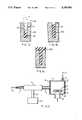
- FIG. 2is a schematic configuration illustrating the apparatus according to one of the embodiments of this invention to be used for this process.
- the configuration of this apparatusis given below.
- a reaction vessel 1In a reaction vessel 1 is accommodated a substrate 3 located on a sample holder 2. To the reaction vessel 1, active species of a first reactive gas 6 and a second reactive gas 7 are introduced through the gas introducing pipes 4 and 5, and are exhausted through the exhaust pipe 8 connected to the exhausting system. The flow rate of the first and the second reactive gases can be adjusted with a mass-flow controller (not shown). The first reactive gas 6 is activated in a microwave discharge portion 9 connected to the above mentioned gas introducing pipe 4.
- the gas introducing pipe 4is made of a quartz in this embodiment.
- Microwave poweris supplied from a microwave power source 10 through a waveguide 11 to the discharge portion 9.
- Activation of the reactive gas 6is performed with the plasma in this embodiment, but it may be done with the thermal excitation, optical excitation or electron beam excitation.
- Pressure in the vessel 1is set by changing the conductance of a valve (not shown), and is measured with a diaphragm vacuum gauge (not shown) to be controlled.
- a cooling means 12is provided to cool the substrate 3, and an additional heating means 13 can be provided, if required. These means are connected to a control system (not shown) to monitor the temperature of the substrate 3 and keep it at a fixed value not more than the liquefaction point of the active species generated from the first reactive gas, the second reactive gas and their reaction products.
- the cooling means 12carries a nitrogen gas coming through a liquid nitrogen to the holder 2 via a cooling pipe (not shown).
- the cooling meansis controlled by adjusting the flow rate of the nitrogen gas with a needle valve (not shown) provided in the cooling pipe.
- a heateris used for the heating means 13, but the cooling and the heating means are not limited to those described above, and anything that can keep a constant temperature is acceptable.
- the substrateis fixed to the above mentioned sample holder so that the substrate can make good thermal contact with the sample holder.
- Areas of the substrate other than the reaction vessel 1 and the sample holder 2may have a structure, for example, with an electric current heater wound around the wall of the vessel 1, to maintain the space in the reaction vessel 1.
- FIG. 3As a thin film forming apparatus relating to this invention, other embodiments shown in FIG. 3 and 4 may be utilized.
- the apparatus shown in FIG. 3is almost the same as the configuration of the apparatus of FIG. 1, and the same parts are shown with the same reference numbers.
- the difference of this apparatus from the one in FIG. 2is that a light radiation means 16 to radiate a beam 15, e.g., electron, ion or laser beams, is provided.
- This light radiation means 16enables excitation of the reactive gas with a light. By using this light excitation, as with the apparatus shown in FIG. 2, the damage to the substrate 2 and other adverse influences may be reduced.
- the substrate 3extends into an out of the reaction vessel 1 through another adjacent chamber.
- This chambermay be evacuated, or may contain the inert gas with atmospheric or higher pressure.
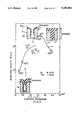
- the thin film forming apparatus shown in FIG. 4also has almost the same configuration as the one shown in FIG. 2, and the same parts as the FIG. 2 are indicated with the same reference numbers.
- These reference numbersshow a thin film forming apparatus capable of post treatment after the thin film is formed.
- the substrate 3is carried through a carrying system 17 to a thermal treatment chamber 18 by a carrying mechanism (not shown).
- the substrate 3 carried to the thermal treatment chamber 18is placed on a holder 20 equipped with a heating means 19, and a thermal treatment is applied to the substrate. This heating may be conducted by raising the substrate temperature instantaneously with radiation from an infrared lamp 21.
- a reference number 22indicates a gas inlet port for introducing an inert gas Z 23, and the reference number 24 is a gate valve dividing the reaction vessel 1 and the thermal treatment chamber 18.
- oxygen (O 2 )is used as a first reactive gas
- tetramethylsilane (Si(CH 3 ) 4 ; TMS)is used as a second reactive gas
- a silicon substrateas a substrate
- a silicon oxide filmis deposited on this silicon substrate.
- oxygen gas 6, which is the first reactive gasis introduced through the gas introducing pipe 4 and microwaves of 2.45 GHz are discharged to produce an oxygen radical (O*).
- O*oxygen radical
- TMSis introduced to the reaction vessel 1 without discharging.
- the total pressure in the reaction vessel 1is fixed at 2 Torr.
- the sample holder 2has a built-in stainless steel pipe 12. Cooling nitrogen (N 2 ) gas passes through the liquid nitrogen and flows through the pipe 12 to be lower the temperature of the substrate 3.
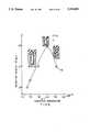
- FIG. 5shows the deposition velocity of the silicon oxide film at variable substrate temperatures in the above process, and the resulting configuration of a trench on the substrate.
- the flow rates of oxygen and TMSare 56 SCCM and 7 SCCM, respectively, and the trench has an aspect ratio of 1.5.
- the intensive deposition on the trench cornersdecreases and at the substrate temperature of -20° C. or less, the thin film can fully fill the trench.
- FIG. 6shows the deposition velocity and the deposition configuration at the different substrate temperatures when the flow ratio of oxygen to TMS is 24. Conditions other than the flow ratio are the same as in FIG. 5.
- FIG. 6shows a tendency similar to that seen in FIG. 5. It is observed that this process is optimum for the formation of an interlaminar insulation film in the multilayer wiring technique.
- FIG. 7is a phase diagram of hexamethyldisiloxane and trimethylsilanol which can be reaction products by tetramethylsilane (TMS)-oxygen (O 2 ) active species and tetramethylsilane.
- TMStetramethylsilane
- O 2oxygen
- the trench interiorcan be filled if the substrate temperature is lowered to about -20° C. It is assumed from this phase diagram that the liquid used in the deposition includes tetramethylsilane and/or hexamethyldisiloxane at a substrate temperature in the range of 20° C. -100° C. and a vessel internal pressure of less than 10 Torr.
- the substrate temperatureis required to be not more than -22° C. where hexamethyldisiloxane is liquid and not less than -100° C. where tetramethylsilane is a solid.
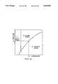
- FIG. 8is a diagram to show the deposition velocity and the deposition configuration with changes of internal pressure of the reaction vessel.
- the substrate temperatureis set at -40° C., and the flow rate of TMS and oxygen at 7 SCCM and 168 SCCM respectively.
- the depositionforms a large lump on the substrate surface around 10 Torr, and the trench cannot be filled.
- the pressuredecreases, however, filling becomes possible and the deposition velocity increases.
- the shape of a globule 90 adhered on the substrate surface as a lumpcan be expressed by the formula below in the coordinates shown in FIG. 9, using a Laplace equation:
- the reference number 91indicates the substrate; the main curvature of the curved surface in the plane of the figure is r/sin ⁇ , and the main curvature perpendicular to this is R, ⁇ represents the surface tension, ⁇ is the liquid density and ⁇ P 0 is the pressure difference between the inside and the outside of the globule 90. If the globule 90 is rotation symmetry and the two main curvatures at the apexes are equally b, according to the equation above,
- the appropriate pressureshould not be less than the temperature of the triple point of hexamethyldisiloxane or tetramethylsilane, so that they will be liquefied.
- FIG. 11shows the deposition velocity and deposition configuration change to the flow ratio of oxygen and tetramethylsilane. From this figure, it is seen that the deposition velocity reaches its peak when the oxygen/TMS flow ratio is around 20.
- the trenchcan be filled with an approximate oxygen/TMS flow ratio of 4, and the trenches will can be filled at ratios not less than this value.
- the reason for this phenomenonis considered to be the fact that, in the formation of hexamethyldisiloxane from oxygen and TMS, the following reaction occurs. ##STR1## where, oxygen/TMS equals 2. Therefore, when tetramethylsilane is 7 SCCM, the oxygen is required to be 14 SCCM or more, and the flow ratio is preferably at least 2 or more for an ideal reaction.
- FIG. 12shows infrared absorption spectra of a deposited film for oxygen/TMS flow ratios of 8 (graph A), 24 (graph B) and 40 (graph C). An absorption peak of Si--O--Si is observed in the range from 1200 cm -1 to 1000 cm -1 , and the film is confirmed to be the silicon oxide film.
- the oxygen/TMS flow ratios at varying velocities of etching on the deposited filmare determined using a solution including 6% of HF and 30% of NH 3 F. These determined values show that, as oxygen/TMS increases, the etching velocity decreases and the film is further nitrogenized. Thus, it is found preferable to increase the oxygen flow rate and make the oxygen/TMS flow ratio larger for a good quality deposit film.
- the substrateis thermally treated in the reaction vessel with the two methods below.
- the absorption strength changes of Si--CH 3 , Si--H and O--H specified with the Si--O--Si peak absorption of the infrared absorption spectra for the film obtained from the above versus oxygen/TMS flow ratiois shown in FIG. 15.
- the combination of Si--CH 3 and O--Hdecreases first during the thermal treatment of (1), and second during the thermal treatment in (2), and the silicon oxidization proceeds. It was found that the combination of Si--H disappears during the treatment processes of (1) and (2).
- the substrate temperatureshould be at least 300° C.
- the thermal treatment in (1) and (2) abovecan promote oxidization of silicon, and it has been observed that, in particular, the oxidization caused by the thermal treatment process (2) is remarkable.
- Radiation of an ArF excimer laser with a wave length of 193 nm during the film formingactivates the liquefied layer or substrate surface, resulting in a further flatness of the filled trench through experiments. Radiation energy of the ArF excimer laser is then 330 Joul/cm 2 sec. As the activation proceeds more when the energy is not less than this value, this activation will occur when the energy is 330 Joul/cm 2 or higher. This activation is performed by an impact with ions, electrons, etc., on the substrate surface, and this will enhance the surface migration of the active species to the thin film to promote the flatness of the filled trench surface.
- the above-mentioned thin film forming apparatushave separated vessels including one for plasma forming and another for the reaction.
- the inventionmay be also applied to the one vessel type thin film forming apparatus.
- FIG. 16is a schematic view showing a thin film forming apparatus according to one embodiment of this invention.
- 101denotes a grounded vacuum vessel forming the reaction vessel.
- Prescribed first and second reactive gasesare introduced into the reaction vessel 101 through a gas inlet 102.
- the mixed gas contained in the reaction vesselis exhausted through a gas outlet 103.
- a cathode (first electrode) 105is disposed opposite the top wall of the vacuum vessel serving as an anode (second electrode).
- the first electrodeOn the first electrode is placed a substrate 106, and a cooled nitrogen gas is passed over this electrode for cooling.
- a heating device(not shown) is also provided to raise the temperature.
- the first electrodeis connected to a high frequency power source 109 through a matching circuit 108.
- a heater 111is coiled around a wall matching circuit 108.
- a heater 111is coiled around a wall 110 of the reaction vessel 101, thereby preventing adhesion of the deposition film.
- another vacuum vesselwhich is vacuous or filled with an inert gas is disposed between the above reaction vessel 101 and the atmosphere for loading and unloading substrate 106.
- reaction vessela so-called load-lock type.
- 116denotes an insulator.
- FIG. 17Parts identical with those shown in FIG. 16 are assigned the same reference numbers.
- a thin filmwas deposited on a substrate 106 in the same way as in the above embodiment and the substrate 106 was moved to another reaction vessel 112 with a carrier (not shown) and placed on a holder 113 and heated thereon by a heating means (not shown).
- this heating treatmentmay be effected by raising the substrate temperature instantaneously with an infrared lamp irradiated just above the substrate 106, for example.
- an inert gas or the first reactive gasmay be introduced through a gas inlet 102a during this heating treatment.
- a high frequency power source 109is connected via a matching circuit 108, so that the plasma can be generated during the heating treatment.
- a gate valvedenotes a gate valve.
- This inventionmay be applied in various ways. For example, a magnetic field may be supplied from outside between parallel plate electrodes applied with the above RF power as a means to generate the plasma, thereby generating a high-density plasma.
- electrical dischargemay be generated by ECR (Electron Cyclotron Resonance) discharge, a hollow cathode discharge, or by suppling high frequency power from outside with the substrate disposed in a vacuum vessel of an insulator, such as a quartz.
- ECRElectro Cyclotron Resonance
- FIG. 18shows how the silicon oxide film is formed on the silicon substrate.
- the lateral axisindicates the temperatures of the substrate and the vertical axis shows the deposition velocity.
- the cross sectionsshow different filled shapes formed within the trench of the substrate.
- the plasmais generated by applying an RF power of 13.56 MHz between the first and second electrodes to cause a high frequency electrical discharge.
- oxygenis introduced at a ratio of 40 cc/minute and TMS 5 cc/minute.
- the total pressureis 5 ⁇ 10 -3 Torr.
- a magnetis disposed on the second electrode side to allow high-density plasma to be obtained. It is seen from FIG. 18 that the deposition velocity exhibits a maximum value with respect to changes of the substrate temperature. It is seen by observing the filled shape within the trench, that when the aspect ratio of the trench is one or more, SiO 2 produced by the reaction of the oxygen radical and TMS in the gaseous phase at a temperature above room temperature as shown in FIG. 18(c) is deposited on the substrate similar to falling snow, as seen in the so-called conventional plasma CVD process, and the cavity is formed.
- the oxidationproceeds accompanying the inclusion of the oxygen radical and the tacking in of the oxygen ions.
- the above liquid layeris finely dispersed over the substrate surface and therefore it exists most stably on the bottom corner of the trench to provide a large contact area in the substrate surface.
- the depositis first formed on the corner. Therefore, as shown in FIG. 19, the deposit accumulates from the bottom of the trench upward to form a film, making it possible to fill a trench with a high aspect ratio and to provide a very even surface, which could not be done heretofore.
- a film at a low temperatureis effective for the formation of an interlaminar insulation film in the multilayered wiring process.
- a silicon nitride filmSi 3 N 4
- oxide and nitridecan be formed readily.
- the gas pressure in the reaction vesselis not limited to the above-mentioned 10 -3 Torr but can be selected to fall in the most effective pressure range according to the discharging method and the reactive gas used.
- the reaction gas to be usedmay be one type and a desired film may be deposited by a process such as thermal decomposition. It was experimentally confirmed that in the process of forming the film, the irradiation with an excimer laser having a wavelength of 193 nm, or with ions, electrons or the like, enhances the activity of the above liquefied layer, increasing the surface migration of the active species within the layer and completing the filling of the trenches, making the film completely flat.
- an inert gassuch as argon or helium
- the oxide film producedincludes these impurities.
- This filmfills the trench. Then it is heated instantaneously with a heater or a lamp, for example. This disperses the impurities into the silicon substrate.
- an oxide film containing the impurities along the wallswas produced by the thermal CVD process.
- the concentration of the impurities contained in the oxide film which is formed along the side walls of the trenchis lower than in the planar portion. Thus, a desired specific resistance could not be attained from the side walls.
- the oxide film according to the present inventionincludes the impurities in a very uniform amount as shown in FIG. 19 describing the depositing state with the lapse of time. Therefore, after depositing, as shown in FIG. 20, a thermal treatment is given to remedy the above drawbacks completely.
- the dispersion layer as shown in FIG. 20is essential to provide a sufficient memory capacity for large scale memory devices, such as 16M and 64M DRAMs.
- the above thermal treatmentwhen effected after the film formation, for example in situ within the treating chamber as shown in FIG. 16 or FIG. 17, can completely avoid the contamination by the impurities other than the prescribed impurities, such as carbon, nickel and other heavy metals. Thus, a high quality film is deposited.
- gas containing a hydrogen and a halogen element in the reactive gasreduces the methyl group contained in the TMS, and more stable CH 4 and CH 3 Cl are produced and removed, resulting in the lowering of the concentration of the carbon impurities.
- AsH 4is used as an impurity to be added to the second reaction gas in this example, but in case of phosphor (P) diffusion, a material such as POCl 3 , PCl 3 and PH 3 which reacts with the first or second reactive gas element to produce phosphor, may be used. In case of boron (B) diffusion, BCl 3 , B 2 H 6 , etc., may be used.
- metalscan entirely fill in a space with a high aspect ratio, such as a contact hole.
- the deposition of silicon and germaniumcan be done.
- As(CH 3 ) 3 , AsH 3 , Ga(CH 3 ) 3 and GaH 3GaAs and other group III-V compounds can be deposited and using a reactive gas containing indium and phosphor, InP and other group II-VI compounds can be deposited.
- a reactive gas containing at least carbon and hydrogenvarious high molecular organic films can be deposited.
- MMAmethylmethacrylate
- PMMAwhich is used for an electron beam resist
- the substrate used herehas an unevenly configuraed surface provided with the trench having an aspect ratio of one or more.
- Nitrogen (N 2 ) gasis used as the first reactive gas, and N* radical is introduced into the reaction vessel by discharging.
- Methylmethacrylate (MMA)is introduced as the second reactive gas and the exhaustion is conducted.
- the substrate temperatureis cooled to -30° C. or less. This results in the covering of the unevenness on the surface of the substrate with a film of PMMA, a polymer of MMA, for the same principle as the one illustrated in FIG. 1, to achieve a super flatness.
- the PMMA filmis, as everyone knows, widely used as an electron beam resist.
- FIG. 21is the sectional view of the final process showing the formation of the source, a drain electrode and a wiring for a MOS transistor using the process of this embodiment.
- a gate oxide film 71 and a gate electrode 72are formed on a silicon substrate 70, and the source and the drain areas 73, 74 are integrally formed to the gate. After the coating of the entire surface with a silicon oxide film 75 using a CVD process, etc., the silicon oxide film 75 on the source and the drain 73, 74 is partially removed by etching to form a contact holes 76 with an aspect ratio of one or more.
- a wiring 77 for the source and the drain electrodesis next formed with the method of this invention.
- hydrogenis used as the first reactive gas and Al(CH 3 ) 3 as the second reactive gas
- the substrate temperatureis set at a specified value to fill the alminium electrode wiring 77 completely into the contact hole 76 and form a super flatness by repeated deposition.
- a silicon oxide film 78is formed as protective film all over the surface. This protective film 78 can be formed by the process of this invention.
- a flat filmcan be formed.
- the mechanical vibration of the substrate 70 during the forming of the electrode wiring 77disturbs a trench retaining layer (a stagnant layer) of the gaseous phase to promote the deposition of the alminium film on the substrate 70.
- Such vibration of the substrate itself, or the gaseous phase during the thin film formingis effective to increase the deposition velocity and to improve the film quality.
- a motormay be provided at the sample holder 2, as shown in FIGS. 2 through 4, to produce the mechanical vibration, or a supersonic wave oscillator may be incorporated in the holder 2.
- the second reactive gascan be Ti(C 2 H 5 ) 2 , carbonyl metal, such as W(CO) 6 or Cr(CO) 6 , or halide metal, etc., instead of Al(CH 3 ) 3 .
- gases at least including an oxidesuch as N 2 O
- gases at least including an oxidesuch as N 2 O
- nitrogen or NH 3formation of a silicon nitride film is possible.
- the oxide filmscan produce the nitride.
- the substrate temperature at that timecan be set at a value not more than the liquefaction points of the active species of the first reactive gas, the second reactive gas and their reaction product, depending on the type of gases.
- inert gasessuch as argon or helium
- first reactive gasMixing inert gases such as argon or helium with the first reactive gas generates long-life metastable active species of these inert gases.
- active speciescan carry the active species of the first reactive gas, and this results in high flexibility of the device design.
- silicon or germanium depositionis possible using hydrogen as the first reactive gas and using a gas containing at least germanium or silicon such as GeH 4 , SiH 4 , SiCl 4 and GeCl 4 as the second reactive gas.
- Group III to V compound, such as GaAscan be deposited when the second reactive gas is As(CH 3 ), AsH 3 , Ga(CH) 3 or GaH 3 , and group II-VI compounds, such as InP, may be used when some reactive gas includes indium and phosphor.
- the rotating mechanismcan be connected to the sample holder 12 for supporting the substrate 3 so that the substrate 3 is rotated at a high velocity and the reactive gas diffuses uniformly.
- the rotationmay be at a fixed velocity, or may be intermittent to avoid a rotation of the gaseous phase with the substrate.
- the configuration abovecan increase the deposition velocity more, and reduce variations in the deposition velocity and the deposition film composition on the substrate. Such variations result from the difference of the distance from the gas inlet port 4 and 5 to the surface of the substrate 3, even in the case of a large-sized substrate, such as a silicon wafer. For radiation by electrons, ions and light, such as laser beam, this is convenient because it can compensate for beam variations, and a large diameter beam is not necessary.
- a plurality of substratescan be simultaneously introduced to the reaction vessel in FIGS. 2 through 4.
- a reaction vessel in the shape of a rectangular parallelepipedfour surfaces are provided with substrates, another substrate is used for putting in and taking out of the substrates, and an other surface for vacuum exhaust and the introduction of the first and the second reactive gas.
- each substrateis placed an equal distance from the gas inlet port to form a uniform thin film.
- the inventioncan achieve a better filling than with the prior art without causing radiation damage of insulation, semiconductor, metal, etc., to realize a flatness even for the trench with a high aspect ratio.
Landscapes
- Engineering & Computer Science (AREA)
- Chemical & Material Sciences (AREA)
- Physics & Mathematics (AREA)
- Computer Hardware Design (AREA)
- Microelectronics & Electronic Packaging (AREA)
- Power Engineering (AREA)
- Manufacturing & Machinery (AREA)
- General Physics & Mathematics (AREA)
- Condensed Matter Physics & Semiconductors (AREA)
- Chemical Kinetics & Catalysis (AREA)
- Organic Chemistry (AREA)
- Metallurgy (AREA)
- General Chemical & Material Sciences (AREA)
- Materials Engineering (AREA)
- Mechanical Engineering (AREA)
- Plasma & Fusion (AREA)
- Inorganic Chemistry (AREA)
- Formation Of Insulating Films (AREA)
- Chemical Vapour Deposition (AREA)
Abstract
Description
This application is a continuation of application Ser. No. 07/169,577, filed Mar. 17, 1988, now abandoned.
1. Field of the Invention
This invention relates generally to a thin film forming method and a thin film forming apparatus, and more particularly to a method and apparatus for forming a thin film on a surface of a substrate having a trench or an unevenness thereon, e.g., a semiconductor substrate.
2. Description of the Prior Art
The processes usually used to form a thin film on a surface of a substrate, such as a semiconductor, are classified broadly into Chemical Vapor Deposition (CVD) and Physical Vapor Deposition (PVD).
The CVD process induces a chemical reaction on the substrate surface or in gaseous phase to form a thin film on the substrate, and this process is used to form insulation films such as a silicon oxide film or a silicon nitride film. The PVD process forms a thin film utilizing collision against a substrate of depositing materials generated in the gaseous phase, and this process is mainly used for metal film forming.
To achieve satisfactory results, VLSI device fabrication presently requires that thin film is deposited within a trench formed in the substrate having an aspect ratio one or more (depth/width).
FIG. 22 is a sectional diagram to show a typical conventional plasma CVD process of the prior art (for example, J. L. Vossen & W. Kern, Thin Film Processes: Academic Press, 1978). In this process, aninsulating film 53 is formed by depositing thedeposit materials 52, which is in the solid phase generated in gaseous phase within atrench 51 of high aspect ratio formed on asubstrate 50, snch as silicon. However, the deposit material is deposited heavily on aedge 54 of thetrench 51, thereby obstructing other deposit material from entering toward a bottom 55 of thetrench 51. Thus, acavity 56 is formed within thetrench 51 and there is a degradation of stage coating properties on the substrate surface.
To cope with the above problem, a process called the bias sputtering process, which is one of the PVD processes, is employed (for example, T. Mogami, M. Morimoto & H. Okabayashi: Extended Abstracts 16th Conf. Solid State Devices & Materials, Kobe, 1984, p. 43). This method is to form an insulating film, such as a silicon oxide film, by physically sputtering the substrate surface with ions of argon, for example. In the application of this method, the sputtering makes it difficult to have much deposition on edges, as shown in FIG. 22, and promotes heavier deposition on the flat surface portions. Therefore, the problems of forming thecavity 56 and of the stage coating properties are reduced in comparison to the CVD process above.
However, as the deposit material in gaseous phase comes into the trench on a slant, it is difficult to achieve a good filling within the trench with an aspect ratio of one or more. This method actually has a low deposition velocity, which means a very low productivity, because of the competing reactions between the removal of the deposited film and the film deposition by physical sputtering. In addition, the radiation damage is inevitable because the process is conducted in the plasma.
Recently, an ECR bias sputtering method (for example, H. Oikawa; SEMI TECHNOLOGY SYM, 1986, E3-1) was proposed to reduce the oblique incident element of the deposit material within the trench. This method lessens the above-mentioned problem of the oblique incidence of the deposition material within the trench even though the deposit material is in the solid state, but it is not a complete solution. Appropriate forming of a thin film with a trench of the high aspect ratio is still difficult.
Other than the processes described above, a method to form a silicon oxide film using thermal decomposition method a TEOS (R. D. Rung, T. Momose & Nagakubo; IEDM. Tech. Dig. 1982, p. 237) has been proposed. This method as shown in FIG. 23 (a) has a large surface movement rate of the deposit material, which makes cavity forming difficult, and realizes good stage coating properties. However, when anoxide film 57 having trenchs formed by this method is cleaned, for example with diluted HF solution, the removal velocity of theoxide film 57 at the center of thetrench 51 is extremely high, as shown in FIG. 23 (b), and as a result, the flat filling actually cannot be achieved. The reason seems to be the fact that the distortion of the oxide film grown from both sides of the trench remains around the center. It is thus considered extremely difficult to fill a trench with a high aspect ratio, even when a conformable thin film forming method is employed.
In FIG. 23 (a), after formation of an oxide film with impurity as a solid phase diffusing source using the thermal CVD method etc., a thermal process may be applied to diffuse the impurity around the trench of the substrate. However, when comparing an oxide film formed on the side wall of the trench and that on a flat surface, the former has less impurity density, and a desired resistivity cannot be obtained with this method.
It is an object of the invention to provide an improved thin film forming process and a forming apparatus for this process which enables a good filling within a trench of high aspect ratio with films of an insulating material, a semiconductor material, and a metal, etc.
This invention solves the problems of the prior art in thin film forming with a trench having a high aspect ratio formed on above-mentioned substrate, such as semiconductors etc., such as cavity forming in the trench, degraded stage coating properties on the substrate surface, or radiation damage against the substrate.
A more complete appreciation of the invention and many of the attendant advantages thereof will be readily obtained as the same becomes better understood by reference to the following detailed description when considered in connection with the accompanying drawings, wherein:
FIGS. 1(a), 1(b) and 1(c) are sectional views illustrating steps of a method in accordance with the invention;
FIGS. 2, 3 and 4 are partial sectional views illustrating forming apparatus in accordance with several embodiments of the invention;
FIGS. 5 and 6 are graphs illustrating functions in accordance with embodiments of the invention;
FIG. 7 is a state diagram illustrating relationships of pressure and temperature in accordance with the embodiment of the invention;
FIG. 8 is a graph illustrating the relationship of the deposition velocity and the pressure in accordance with the embodiments of the invention;
FIGS. 9, 10(a) and 10(b) are sectional views illustrating the functions in accordance with the embodiment of the invention;
FIGS. 11, 12, 13, 14 and 15 are graphs illustrating different relationships of parameters in accordance with the embodiment of the invention;
FIGS. 16 and 17 are partial sectional views illustrating forming apparatus in accordance with other embodiments of the invention;
FIG. 18 is a graph illustrating the relationship of the deposition velocity and the substrate temperature in accordance with the invention;
FIGS. 19, 20(a) and 20(b) are sectional views illustrating the steps of a method in accordance with the another embodiments of the invention;
FIG. 21 is a sectional view illustrating a semiconductor device in accordance with an other embodiment of the invention;
FIG. 22 is a sectional view illustrating a conventional method;
FIGS. 23(a) and 23(b) are sectional views illustrating steps in accordance with an another conventional method; and
FIG. 24 is a typical state diagram.
This invention provides a thin film forming method together with a device for that method, which cools the substrate not more than the liquefaction point of the deposit species, so that the deposit species in gaseous phase can exist on the substrate surface under more stable conditions than those when the deposit species are flowing in gaseous phase.
Referring to FIG. 1, the function of the thin film forming method of this invention is explained below.
In FIG. 1 (a),deposit species 32 in a gaseous phase state is deposited within atrench 31 with high aspect ratio formed on asubstrate 30, such as a semiconductor. The substrate is cooled to the temperature not more than the liquefaction temperature point of thedeposit species 32, so thespecies 32 liquefies and adheres on the substrate surface. Thereference number 33 is a thin film formed within thetrench 31 by thedeposit species 32.
By repeating this process, as shown in FIG. 1 (b),thin films 33a are built up within atrench 31 to form a filling. If the process is continued after the complete filling up of thetrench 31, thin film 33b is formed appropriately over thetrench 31 and on the surface of thesubstrate 30.
To explain this phenomenon, FIG. 24 shows, with parameters of the temperature and the pressure, three phases (gaseous phase, liquid phase and solid phase) of an active species of a first reactive gas, a second reactive gas, or their reaction product. As the temperature of the material including the reactive gas, etc., described above, decreases, the state changes from the gaseous phase A to the liquid phase B. In a high pressure condition, transfer from gaseous phase A to liquid phase B becomes distinctive.
For example, if a reactive gas with pressure PO is in the state of gaseous phase A, when the temperature is lowered to tO (the boundary between the gaseous phase and the liquid phase, i.e., the liquefaction point) or below, the state changes to the liquid phase.
If the temperature drops more, the state goes to the solid phase. Therefore, this invention utilizes the temperature dependency of three phases above for the trench filling in semiconductor fabrication. When only one kind of gas is used, the substrate temperature shall be set not more than the liquefaction point of that gas.
As described above, this invention provides an excellent flatness after the appropriate filling or plugging of trenchs with a high aspect ratio at low temperature, and is an optimum for VLSI fabrication.
A first embodiment of the thin film forming process according to this invention is described below.
Firstly, an apparatus for this process is explained. FIG. 2 is a schematic configuration illustrating the apparatus according to one of the embodiments of this invention to be used for this process. The configuration of this apparatus is given below.
In areaction vessel 1 is accommodated asubstrate 3 located on asample holder 2. To thereaction vessel 1, active species of a firstreactive gas 6 and a secondreactive gas 7 are introduced through thegas introducing pipes exhaust pipe 8 connected to the exhausting system. The flow rate of the first and the second reactive gases can be adjusted with a mass-flow controller (not shown). The firstreactive gas 6 is activated in amicrowave discharge portion 9 connected to the above mentionedgas introducing pipe 4. Thegas introducing pipe 4 is made of a quartz in this embodiment.
Microwave power is supplied from amicrowave power source 10 through awaveguide 11 to thedischarge portion 9. Activation of thereactive gas 6 is performed with the plasma in this embodiment, but it may be done with the thermal excitation, optical excitation or electron beam excitation. Pressure in thevessel 1 is set by changing the conductance of a valve (not shown), and is measured with a diaphragm vacuum gauge (not shown) to be controlled.
Within the above mentionedholder 2, a cooling means 12 is provided to cool thesubstrate 3, and an additional heating means 13 can be provided, if required. These means are connected to a control system (not shown) to monitor the temperature of thesubstrate 3 and keep it at a fixed value not more than the liquefaction point of the active species generated from the first reactive gas, the second reactive gas and their reaction products.
The cooling means 12 carries a nitrogen gas coming through a liquid nitrogen to theholder 2 via a cooling pipe (not shown). The cooling means is controlled by adjusting the flow rate of the nitrogen gas with a needle valve (not shown) provided in the cooling pipe. A heater is used for the heating means 13, but the cooling and the heating means are not limited to those described above, and anything that can keep a constant temperature is acceptable. The substrate is fixed to the above mentioned sample holder so that the substrate can make good thermal contact with the sample holder.
Areas of the substrate other than thereaction vessel 1 and thesample holder 2 may have a structure, for example, with an electric current heater wound around the wall of thevessel 1, to maintain the space in thereaction vessel 1.
As a thin film forming apparatus relating to this invention, other embodiments shown in FIG. 3 and 4 may be utilized. The apparatus shown in FIG. 3 is almost the same as the configuration of the apparatus of FIG. 1, and the same parts are shown with the same reference numbers. The difference of this apparatus from the one in FIG. 2 is that a light radiation means 16 to radiate abeam 15, e.g., electron, ion or laser beams, is provided. This light radiation means 16 enables excitation of the reactive gas with a light. By using this light excitation, as with the apparatus shown in FIG. 2, the damage to thesubstrate 2 and other adverse influences may be reduced.
Although it is not shown in the figures, thesubstrate 3 extends into an out of thereaction vessel 1 through another adjacent chamber. This chamber may be evacuated, or may contain the inert gas with atmospheric or higher pressure. By this "load-locking" of thereaction vessel 1, reproducibility of the process may be remarkably improved.
The thin film forming apparatus shown in FIG. 4 also has almost the same configuration as the one shown in FIG. 2, and the same parts as the FIG. 2 are indicated with the same reference numbers. These reference numbers show a thin film forming apparatus capable of post treatment after the thin film is formed. In this apparatus, after the thin film forming on thesubstrate 3, thesubstrate 3 is carried through a carryingsystem 17 to athermal treatment chamber 18 by a carrying mechanism (not shown). Thesubstrate 3 carried to thethermal treatment chamber 18 is placed on aholder 20 equipped with a heating means 19, and a thermal treatment is applied to the substrate. This heating may be conducted by raising the substrate temperature instantaneously with radiation from aninfrared lamp 21.
By conducting the thermal treatment above, residue, dust, etc., on the surface of thesubstrate 3 can be removed, and the film quality of the thin film can be improved.
In the same figure, areference number 22 indicates a gas inlet port for introducing aninert gas Z 23, and thereference number 24 is a gate valve dividing thereaction vessel 1 and thethermal treatment chamber 18.
An embodiment of thin film forming process according to this invention is described below. This explanation refers specifically to the apparatus shown in FIG. 2, but any of the apparatus described above can be used for this process.
In this embodiment, oxygen (O2) is used as a first reactive gas, and tetramethylsilane (Si(CH3)4 ; TMS) as a second reactive gas. Using a silicon substrate as a substrate, a silicon oxide film is deposited on this silicon substrate. First,oxygen gas 6, which is the first reactive gas, is introduced through thegas introducing pipe 4 and microwaves of 2.45 GHz are discharged to produce an oxygen radical (O*). Then, this oxygen radical is moved to thereaction vessel 1. Meanwhile, TMS is introduced to thereaction vessel 1 without discharging. The total pressure in thereaction vessel 1 is fixed at 2 Torr. Thesample holder 2 has a built-instainless steel pipe 12. Cooling nitrogen (N2) gas passes through the liquid nitrogen and flows through thepipe 12 to be lower the temperature of thesubstrate 3.
FIG. 5 shows the deposition velocity of the silicon oxide film at variable substrate temperatures in the above process, and the resulting configuration of a trench on the substrate. The flow rates of oxygen and TMS are 56 SCCM and 7 SCCM, respectively, and the trench has an aspect ratio of 1.5.
It is seen from this graph that the deposition velocity represented by the curve A reaches the highest point when the substrate temperature is -40° C. For the filled trench configuration, at a temperature above room temperature, the silicon oxide film formed by the reaction of the O* radical and TMS forms a cavity as described in the prior art.
On the other hand, with the decrease of the substrate temperature, the intensive deposition on the trench corners decreases and at the substrate temperature of -20° C. or less, the thin film can fully fill the trench.
FIG. 6 shows the deposition velocity and the deposition configuration at the different substrate temperatures when the flow ratio of oxygen to TMS is 24. Conditions other than the flow ratio are the same as in FIG. 5. FIG. 6 shows a tendency similar to that seen in FIG. 5. It is observed that this process is optimum for the formation of an interlaminar insulation film in the multilayer wiring technique.
The inventors of this invention have made a further study to find optimum conditions for forming a thin film within a trench. Details are described below.
FIG. 7 is a phase diagram of hexamethyldisiloxane and trimethylsilanol which can be reaction products by tetramethylsilane (TMS)-oxygen (O2) active species and tetramethylsilane. As described in the embodiment above, when the interior pressure of the reaction vessel is 2 Torr, the trench interior can be filled if the substrate temperature is lowered to about -20° C. It is assumed from this phase diagram that the liquid used in the deposition includes tetramethylsilane and/or hexamethyldisiloxane at a substrate temperature in the range of 20° C. -100° C. and a vessel internal pressure of less than 10 Torr. It is also considered that oxidation proceeds while entrapping active oxide species in the liquid layer. This assumption may be reasonable since the infrared absorption spectra of this film is nearly identical to that of the plasma polymerization film of hexamethyldisiloxane.
Thus, when the internal pressure of the reaction vessel is 2 Torr, the substrate temperature is required to be not more than -22° C. where hexamethyldisiloxane is liquid and not less than -100° C. where tetramethylsilane is a solid.
Consequently, it is necessary to arrange an appropriate thermal contact between the substrate and the sample holder, an uniform distribution of sample temperature, and a correctly measured and controlled temperature to make the liquefaction possible.
FIG. 8 is a diagram to show the deposition velocity and the deposition configuration with changes of internal pressure of the reaction vessel. The substrate temperature is set at -40° C., and the flow rate of TMS and oxygen at 7 SCCM and 168 SCCM respectively. As a result, the deposition forms a large lump on the substrate surface around 10 Torr, and the trench cannot be filled. As the pressure decreases, however, filling becomes possible and the deposition velocity increases.
The shape of aglobule 90 adhered on the substrate surface as a lump can be expressed by the formula below in the coordinates shown in FIG. 9, using a Laplace equation:
γ(1/R+Sinφ/r)=ρgz+ΔP.sub.0
where, thereference number 91 indicates the substrate; the main curvature of the curved surface in the plane of the figure is r/sinφ, and the main curvature perpendicular to this is R, γ represents the surface tension, ρ is the liquid density and ΔP0 is the pressure difference between the inside and the outside of theglobule 90. If theglobule 90 is rotation symmetry and the two main curvatures at the apexes are equally b, according to the equation above,
γ.2/b=ΔP.sub.0
This means that when the pressure difference ΔP0 is larger with an equal surface tension γ, the radius of curvature b of the apexes becomes smaller, and results in a long shaped globule as shown in FIGS. 10a and 10b. As the pressure of the microwave discharge changes, the types and the quantity of the oxygen active species may change, the functional group produced on the silicon substrate surface may change, and the contact angle to the hexamethyldisiloxane or tetramethylsilane may change.
For these reasons, even in the pressure and temperature range of liquefaction, it is suitable to set the pressure at the contact angle in the range where liquid flows into the inside of the trench, and it is preferable to have a pressure of 10 Torr or less for to process of this embodiment.
The appropriate pressure should not be less than the temperature of the triple point of hexamethyldisiloxane or tetramethylsilane, so that they will be liquefied.
FIG. 11 shows the deposition velocity and deposition configuration change to the flow ratio of oxygen and tetramethylsilane. From this figure, it is seen that the deposition velocity reaches its peak when the oxygen/TMS flow ratio is around 20. The trench can be filled with an approximate oxygen/TMS flow ratio of 4, and the trenches will can be filled at ratios not less than this value. The reason for this phenomenon is considered to be the fact that, in the formation of hexamethyldisiloxane from oxygen and TMS, the following reaction occurs. ##STR1## where, oxygen/TMS equals 2. Therefore, when tetramethylsilane is 7 SCCM, the oxygen is required to be 14 SCCM or more, and the flow ratio is preferably at least 2 or more for an ideal reaction.
FIG. 12 shows infrared absorption spectra of a deposited film for oxygen/TMS flow ratios of 8 (graph A), 24 (graph B) and 40 (graph C). An absorption peak of Si--O--Si is observed in the range from 1200 cm-1 to 1000 cm-1, and the film is confirmed to be the silicon oxide film.
Strength changes of the absorption peaks of Si--CH3, Si-H, O--H specified by this Si--O--Si absorption peak to oxygen/TMS flow ratio as shown in FIG. 13. From this figure, it is seen that the larger the oxygen/TMS becomes, the more the silicon oxides. Reference numbers incircles 1 through 7 correspond to the references in FIG. 12.
Next, a study on the characteristics of the thin film formed with the present invention is described below. As shown in FIG. 14, the oxygen/TMS flow ratios at varying velocities of etching on the deposited film are determined using a solution including 6% of HF and 30% of NH3 F. These determined values show that, as oxygen/TMS increases, the etching velocity decreases and the film is further nitrogenized. Thus, it is found preferable to increase the oxygen flow rate and make the oxygen/TMS flow ratio larger for a good quality deposit film.
After the thin film deposition on the substrate, the substrate is thermally treated in the reaction vessel with the two methods below.
(1) Maintain the substrate temperature at 300° C. in oxygen of 10 Torr for 1 hour.
(2) While discharging microwaves into the oxygen of 2 Torr, maintain the substrate temperature at 300° C. for 1 hour.
The absorption strength changes of Si--CH3, Si--H and O--H specified with the Si--O--Si peak absorption of the infrared absorption spectra for the film obtained from the above versus oxygen/TMS flow ratio is shown in FIG. 15. The combination of Si--CH3 and O--H decreases first during the thermal treatment of (1), and second during the thermal treatment in (2), and the silicon oxidization proceeds. It was found that the combination of Si--H disappears during the treatment processes of (1) and (2). In conclusion, to improve the film quality of the deposited film, the substrate temperature should be at least 300° C. The thermal treatment in (1) and (2) above can promote oxidization of silicon, and it has been observed that, in particular, the oxidization caused by the thermal treatment process (2) is remarkable.
Radiation of an ArF excimer laser with a wave length of 193 nm during the film forming activates the liquefied layer or substrate surface, resulting in a further flatness of the filled trench through experiments. Radiation energy of the ArF excimer laser is then 330 Joul/cm2 sec. As the activation proceeds more when the energy is not less than this value, this activation will occur when the energy is 330 Joul/cm2 or higher. This activation is performed by an impact with ions, electrons, etc., on the substrate surface, and this will enhance the surface migration of the active species to the thin film to promote the flatness of the filled trench surface.
The above-mentioned thin film forming apparatus have separated vessels including one for plasma forming and another for the reaction. The invention may be also applied to the one vessel type thin film forming apparatus.
FIG. 16 is a schematic view showing a thin film forming apparatus according to one embodiment of this invention. In FIG. 16, 101 denotes a grounded vacuum vessel forming the reaction vessel. Prescribed first and second reactive gases are introduced into thereaction vessel 101 through agas inlet 102. The mixed gas contained in the reaction vessel is exhausted through agas outlet 103. In thereaction vessel 101, a cathode (first electrode) 105 is disposed opposite the top wall of the vacuum vessel serving as an anode (second electrode).
On the first electrode is placed asubstrate 106, and a cooled nitrogen gas is passed over this electrode for cooling. A heating device (not shown) is also provided to raise the temperature. Further, the first electrode is connected to a highfrequency power source 109 through amatching circuit 108. Aheater 111 is coiled around awall matching circuit 108. Aheater 111 is coiled around awall 110 of thereaction vessel 101, thereby preventing adhesion of the deposition film. Although it is not illustrated, another vacuum vessel which is vacuous or filled with an inert gas is disposed between theabove reaction vessel 101 and the atmosphere for loading and unloadingsubstrate 106.
Thus, the reliability of the process is greatly enhanced by making the reaction vessel a so-called load-lock type. In the same drawing, 116 denotes an insulator. Further, another embodiment is shown in FIG. 17. Parts identical with those shown in FIG. 16 are assigned the same reference numbers.
In this embodiment, a thin film was deposited on asubstrate 106 in the same way as in the above embodiment and thesubstrate 106 was moved to anotherreaction vessel 112 with a carrier (not shown) and placed on aholder 113 and heated thereon by a heating means (not shown). In addition to the heating from the substrate side, this heating treatment may be effected by raising the substrate temperature instantaneously with an infrared lamp irradiated just above thesubstrate 106, for example. Further, an inert gas or the first reactive gas may be introduced through agas inlet 102a during this heating treatment. Also, a highfrequency power source 109 is connected via amatching circuit 108, so that the plasma can be generated during the heating treatment.
In the drawing,number 115 denotes a gate valve. This invention may be applied in various ways. For example, a magnetic field may be supplied from outside between parallel plate electrodes applied with the above RF power as a means to generate the plasma, thereby generating a high-density plasma. Also, electrical discharge may be generated by ECR (Electron Cyclotron Resonance) discharge, a hollow cathode discharge, or by suppling high frequency power from outside with the substrate disposed in a vacuum vessel of an insulator, such as a quartz.
Another thin film depositing process according to the present invention using the apparatus shown in FIG. 16 will be described below. Oxygen and a tetramethylsilane Si(CH3)4 (TMS) as the first and second reactive gases are inserted into thereaction vessel 101.
FIG. 18 shows how the silicon oxide film is formed on the silicon substrate. The lateral axis indicates the temperatures of the substrate and the vertical axis shows the deposition velocity. The cross sections show different filled shapes formed within the trench of the substrate. The plasma is generated by applying an RF power of 13.56 MHz between the first and second electrodes to cause a high frequency electrical discharge. In the reaction vessel, oxygen is introduced at a ratio of 40 cc/minute andTMS 5 cc/minute. The total pressure is 5×10⁻³ Torr.
A magnet is disposed on the second electrode side to allow high-density plasma to be obtained. It is seen from FIG. 18 that the deposition velocity exhibits a maximum value with respect to changes of the substrate temperature. It is seen by observing the filled shape within the trench, that when the aspect ratio of the trench is one or more, SiO2 produced by the reaction of the oxygen radical and TMS in the gaseous phase at a temperature above room temperature as shown in FIG. 18(c) is deposited on the substrate similar to falling snow, as seen in the so-called conventional plasma CVD process, and the cavity is formed.
On the other hand, it is seen that with a decrease of the substrate temperature, the deposit which is predominantly formed on the corner of the trench is reduced and when the substrate temperature is -20° C. or less the trench can be completely filled. This phenomenon is believed to take place in the following manner. The reaction products of the oxygen radical and TMS, such as hexamethylsiloxane (Si(CH3)2)2 O and trimethyldisiloxane Si(CH3)3 OH, liquefy at the temperatures as shown in FIG. 18 and liquid is formed as a layer on the substrate surface. This liquid layer catches therein SiO2 species which have further reacted in the gaseous phase.
It is believed that the oxidation proceeds accompanying the inclusion of the oxygen radical and the tacking in of the oxygen ions. On the other hand, the above liquid layer is finely dispersed over the substrate surface and therefore it exists most stably on the bottom corner of the trench to provide a large contact area in the substrate surface. As a result, observation of deposition overtime indicates that the deposit is first formed on the corner. Therefore, as shown in FIG. 19, the deposit accumulates from the bottom of the trench upward to form a film, making it possible to fill a trench with a high aspect ratio and to provide a very even surface, which could not be done heretofore.
It is possible also to form a film at a low temperature. This is effective for the formation of an interlaminar insulation film in the multilayered wiring process. Using nitrogen or NH4 instead of oxygen, a silicon nitride film (Si3 N4) can be formed. It is needless to say that by using a material containing at least one element which is included in groups II to VI of the periodic table as the second reactive gas and suitably varying the substrate temperature, oxide and nitride can be formed readily.
It is also needless to mention that the gas pressure in the reaction vessel is not limited to the above-mentioned 10-3 Torr but can be selected to fall in the most effective pressure range according to the discharging method and the reactive gas used.
Addition of an inert gas such as argon or helium to the first reactive gas prolongs the service life of the deposition species as a metastable active species and provides more effective deposition. The reaction gas to be used may be one type and a desired film may be deposited by a process such as thermal decomposition. It was experimentally confirmed that in the process of forming the film, the irradiation with an excimer laser having a wavelength of 193 nm, or with ions, electrons or the like, enhances the activity of the above liquefied layer, increasing the surface migration of the active species within the layer and completing the filling of the trenches, making the film completely flat.
In the formation of the above silicon oxide film, when impurities such as POCl2, PCl3, PH3, BCl3, B2 H6 and AsH4 are added to TMS, for example, the oxide film produced includes these impurities. This film fills the trench. Then it is heated instantaneously with a heater or a lamp, for example. This disperses the impurities into the silicon substrate. Heretofore, an oxide film containing the impurities along the walls was produced by the thermal CVD process. However, the concentration of the impurities contained in the oxide film which is formed along the side walls of the trench is lower than in the planar portion. Thus, a desired specific resistance could not be attained from the side walls.
The oxide film according to the present invention includes the impurities in a very uniform amount as shown in FIG. 19 describing the depositing state with the lapse of time. Therefore, after depositing, as shown in FIG. 20, a thermal treatment is given to remedy the above drawbacks completely. The dispersion layer as shown in FIG. 20 is essential to provide a sufficient memory capacity for large scale memory devices, such as 16M and 64M DRAMs. The above thermal treatment, when effected after the film formation, for example in situ within the treating chamber as shown in FIG. 16 or FIG. 17, can completely avoid the contamination by the impurities other than the prescribed impurities, such as carbon, nickel and other heavy metals. Thus, a high quality film is deposited.
The inclusion of gas containing a hydrogen and a halogen element in the reactive gas reduces the methyl group contained in the TMS, and more stable CH4 and CH3 Cl are produced and removed, resulting in the lowering of the concentration of the carbon impurities. Thus, the film quality is much enhanced. AsH4 is used as an impurity to be added to the second reaction gas in this example, but in case of phosphor (P) diffusion, a material such as POCl3, PCl3 and PH3 which reacts with the first or second reactive gas element to produce phosphor, may be used. In case of boron (B) diffusion, BCl3, B2 H6, etc., may be used. For example, it was confirmed that when the organic metal compounds such as Al(CH3)3, Ti(C5)2, carbonyl metals, such as W(CO)6 and Cr(CO)6, and halogenated metals are used together with hydrogen and nitrogen, metals can entirely fill in a space with a high aspect ratio, such as a contact hole.
In addition to the above thin film forming, using for examples GeH4, SiH4, SiCl4, GeCl4, and a gas including at least silicon, the deposition of silicon and germanium can be done. Using As(CH3)3, AsH3, Ga(CH3)3 and GaH3, GaAs and other group III-V compounds can be deposited and using a reactive gas containing indium and phosphor, InP and other group II-VI compounds can be deposited.
Further, using a reactive gas containing at least carbon and hydrogen, various high molecular organic films can be deposited. For example, when methylmethacrylate (MMA) is introduced and the substrate temperature is lowered to -30° C. or less, PMMA, which is used for an electron beam resist, can be formed.
Proceeding now to the explanation of another embodiment relating to the thin film forming process of this invention, a macromolecule thin film forming process using hydrogen, nitrogen or gases including a halogen element, such as SiCl4, as the first reactive gas, and a gas at least including carbon and hydrogen as the second reactive gas, is described below. This process is basically the same as above-mentioned embodiment, and is briefly described with reference to FIG. 3.
The substrate used here has an unevenly configuraed surface provided with the trench having an aspect ratio of one or more. Nitrogen (N2) gas is used as the first reactive gas, and N* radical is introduced into the reaction vessel by discharging. Methylmethacrylate (MMA) is introduced as the second reactive gas and the exhaustion is conducted.
The substrate temperature is cooled to -30° C. or less. This results in the covering of the unevenness on the surface of the substrate with a film of PMMA, a polymer of MMA, for the same principle as the one illustrated in FIG. 1, to achieve a super flatness. The PMMA film is, as everyone knows, widely used as an electron beam resist.
Another embodiment relating to the thin film forming process of the present invention is explained below. FIG. 21 is the sectional view of the final process showing the formation of the source, a drain electrode and a wiring for a MOS transistor using the process of this embodiment.
Agate oxide film 71 and agate electrode 72 are formed on asilicon substrate 70, and the source and thedrain areas silicon oxide film 75 using a CVD process, etc., thesilicon oxide film 75 on the source and thedrain
Awiring 77 for the source and the drain electrodes is next formed with the method of this invention. In particular hydrogen is used as the first reactive gas and Al(CH3)3 as the second reactive gas, and the substrate temperature is set at a specified value to fill thealminium electrode wiring 77 completely into thecontact hole 76 and form a super flatness by repeated deposition. After patterning of theelectrode wiring 77, asilicon oxide film 78 is formed as protective film all over the surface. Thisprotective film 78 can be formed by the process of this invention. By covering the wiring and the trenches formed by theCVD oxide film 75 with a protective film utilizing the same method as shown in the first embodiment, a flat film can be formed.
In this embodiment, the mechanical vibration of thesubstrate 70 during the forming of theelectrode wiring 77 disturbs a trench retaining layer (a stagnant layer) of the gaseous phase to promote the deposition of the alminium film on thesubstrate 70. Such vibration of the substrate itself, or the gaseous phase during the thin film forming is effective to increase the deposition velocity and to improve the film quality.
As a means to create vibrations, a motor, etc., may be provided at thesample holder 2, as shown in FIGS. 2 through 4, to produce the mechanical vibration, or a supersonic wave oscillator may be incorporated in theholder 2.
Although, alminium is used for the metal filling the trenches, such as the MOS transistor contacts, etc., in this embodiment, the second reactive gas can be Ti(C2 H5)2, carbonyl metal, such as W(CO)6 or Cr(CO)6, or halide metal, etc., instead of Al(CH3)3.
Embodiments of the present invention are explained above and some additional examples are described below. In place of the oxygen discharge in these embodiments, gases at least including an oxide, such as N2 O, can be used. By using nitrogen or NH3, formation of a silicon nitride film is possible. When using a gas including at least one element of the second to sixth group in the periodic table, the oxide films can produce the nitride. The substrate temperature at that time can be set at a value not more than the liquefaction points of the active species of the first reactive gas, the second reactive gas and their reaction product, depending on the type of gases.
Mixing inert gases such as argon or helium with the first reactive gas generates long-life metastable active species of these inert gases. These active species can carry the active species of the first reactive gas, and this results in high flexibility of the device design.
Other than the thin film forming above, for example, silicon or germanium deposition is possible using hydrogen as the first reactive gas and using a gas containing at least germanium or silicon such as GeH4, SiH4, SiCl4 and GeCl4 as the second reactive gas. Group III to V compound, such as GaAs can be deposited when the second reactive gas is As(CH3), AsH3, Ga(CH)3 or GaH3, and group II-VI compounds, such as InP, may be used when some reactive gas includes indium and phosphor.
The thin film forming process explained above using raw material gas of the thin film as the second reactive gas (for example, Al(CH3)4 +H2) can produce the same effect.
In FIGS. 2 through 4, the rotating mechanism can be connected to thesample holder 12 for supporting thesubstrate 3 so that thesubstrate 3 is rotated at a high velocity and the reactive gas diffuses uniformly. The rotation may be at a fixed velocity, or may be intermittent to avoid a rotation of the gaseous phase with the substrate.
The configuration above can increase the deposition velocity more, and reduce variations in the deposition velocity and the deposition film composition on the substrate. Such variations result from the difference of the distance from thegas inlet port substrate 3, even in the case of a large-sized substrate, such as a silicon wafer. For radiation by electrons, ions and light, such as laser beam, this is convenient because it can compensate for beam variations, and a large diameter beam is not necessary.
A plurality of substrates can be simultaneously introduced to the reaction vessel in FIGS. 2 through 4. For example, with a reaction vessel in the shape of a rectangular parallelepiped, four surfaces are provided with substrates, another substrate is used for putting in and taking out of the substrates, and an other surface for vacuum exhaust and the introduction of the first and the second reactive gas. In this case, too, each substrate is placed an equal distance from the gas inlet port to form a uniform thin film.
As explained above, the invention can be changed without departing from the scope of the invention.
The invention can achieve a better filling than with the prior art without causing radiation damage of insulation, semiconductor, metal, etc., to realize a flatness even for the trench with a high aspect ratio.
Claims (51)
1. A thin film forming method, comprising the steps of:
supporting a semiconductor substrate having a trench or an unevenness thereon in a reaction vessel;
introducing a reactive gas into the reaction vessel;
activating the reactive gas to form a deposit species;
exhausting the interior of the reaction vessel; and
cooling the semiconductor substrate below the liquefaction temperature of the deposit species to cause the deposit species to become a material deposited on the semiconductor substrate.
2. The thin film forming method of claim 1 wherein the deposit material includes an active species of the reactive gas.
3. The thin film forming method of claim 1 wherein the deposit material includes reaction products produced during activation of the reactive gas.
4. The thin forming method of claim 1 wherein the step of activating the reactive gas includes the step of generating a plasma.
5. The thin film forming method of claim 1 wherein the step of activating the reactive gas includes the step of thermally activating the reactive gas.
6. The thin film forming method of claim 1 wherein the step of activating the reactive gas includes the step of light activating the reactive gas.
7. The thin film forming method of claim 1 wherein the step of activating the reactive gas includes the step of electron beam activating the reactive gas.
8. The thin film forming method of claim 6 wherein the step of light activating includes the step of laser beam activating the reactive gas.
9. The thin film forming method of claim 1, further comprising the step of heating the semiconductor substrate.
10. The thin film forming method of claim 1 wherein the reactive gas includes an impurity to change the conductivity of the semiconductor substrate.
11. The thin film forming method of claim 1 wherein the aspect ratio of the trench is one or more.
12. The thin film forming method of claim 1 wherein the reactive gas is activated within the reaction vessel supported the substrate therein.
13. The thin film forming method of claim 1 wherein the reactive gas is activated in the other portion of the reaction vessel supporting the substrate therein.
14. The thin film forming method of claim 1 wherein the deposit material is an insulator.
15. The thin film forming method of claim 1 wherein the deposit material is semiconductor.
16. The thin film forming method of claim 1 wherein the deposit material is polymer.
17. The thin film forming method of claim 1 wherein the deposit material is a metal.
18. The thin film forming method of claim 1 wherein the substrate has a mask formed thereon.
19. The thin film forming method of claim 14 wherein insulator is silicon oxide.
20. The thin film forming method of claim 1 wherein the deposit species is heated after the deposit species is formed.
21. The thin film forming method of claim 20 wherein heating is instantaneous.
22. The thin film forming method of claim 1 wherein the substrate is supported electrostatically by a sample holder.
23. The thin film forming method of claim 1 wherein the substrate and the reactive gas are vibrated relatively.
24. The thin film forming method of claim 1 wherein the step of introducing the reactive gas includes the step of supplying two types of gases.
25. The thin film forming method of claim 24 wherein the substrate is semiconductor.
26. The thin film forming method of claim 24, further comprising the step of heating the semiconductor substrate.
27. The thin film forming method of claim 24 wherein the aspect ratio of the trench is one or more.
28. The thin film forming method of claim 24 wherein the deposit material is an insulator.
29. The thin film forming method of claim 24 wherein the deposit material is semiconductor.
30. The thin film forming method of claim 24 wherein the deposit material is polymer.
31. The thin film forming method of claim 24 wherein the deposit material is metal.
32. The thin film forming method of claim 24 wherein the substrate has a mask formed thereon.
33. The thin film forming method of claim 25 wherein the deposit material is an insulator.
34. The thin film forming method of claim 33 wherein insulator is silicon oxide.
35. The thin film forming method of claim 24 wherein the deposit species is heated after the deposit species is formed.
36. The thin film forming method of claim 34 wherein heating is instantaneous.
37. The thin film forming method of claim 24 wherein the substrate is supported electrostatically by a sample holder.
38. The thin film forming method of claim 24 wherein the substrate and the reactive gas are vibrated relatively.
39. The thin film forming method of claim 24 wherein the first reactive gas is activated within the reaction vessel supporting the substrate therein.
40. The thin film forming method of claim 24 wherein the first reactive gas is activated in the other portion of the reaction vessel supporting the substrate therein.
41. The thin film forming method of claim 24 wherein the first reactive gas includes at least one of oxygen, nitrogen, hydrogen or a gas containing at least halogen element.
42. The thin film forming method of claim 24 wherein the first reactive gas includes at least one of inert gases.
43. The thin film forming method of claim 24 wherein the first reactive gas includes at least one of oxygen, nitrogen or hydrogen, and the second reactive gas includes at least one element included in the II to VI groups of the periodic table.
44. The thin film forming method of claim 24 wherein the first reactive gas includes at least one of hydrogen, nitrogen or a gas containing at least halogen element and the second reactive gas includes at least one of organic compound, halide or carbonyl of the metal or semiconductor.
45. The thin film forming method of claim 24 wherein the second reactive gas includes one of tetramethyl silane, hexamethyldisiloxane or trimetyl silanol.
46. The thin film forming method of claim 45 wherein the first reactive gas is oxygen.
47. The thin film forming method of claim 46 wherein the flow ratio of the first reactive gas to the second reactive gas at 2 or more and the temperature of the substrate from 20° C. to -100° C. and keeping the total internal pressure of the reaction vessel less than 10 Torr.
48. The thin film forming method of claim 45 wherein the step of activating includes the step of radiating the laser beam with the power of 330 Joul/cm2 sec.
49. The thin film forming method of claim 47 wherein the step of activating includes the step of radiating the laser beam with the wave length of 200 nm or less and with the power of 330 Joul/cm2 sec.
50. The thin film forming method of claim 47 wherein the pressure in the reaction vessel and the temperature of the substrate are set at a condition where the contact angle of the liquefied globule of the second reactive gas and the substrate becomes acute.
51. The thin film forming method of claim 47 wherein after the formation of the deposit material, the substrate is heated at 300° C. or more with flowing oxygen or oxygen radical.
Priority Applications (4)
| Application Number | Priority Date | Filing Date | Title |
|---|---|---|---|
| US08/203,757US5385763A (en) | 1987-03-18 | 1994-03-01 | Method for forming a film on a substrate by activating a reactive gas |
| US08/323,693US5458919A (en) | 1987-03-18 | 1994-10-18 | Method for forming a film on a substrate by activating a reactive gas |
| US08/474,312US5591486A (en) | 1987-03-18 | 1995-06-07 | Method for forming a film on a substrate by activating a reactive gas |
| US08/728,613US5776557A (en) | 1987-03-18 | 1996-10-10 | Method for forming a film on a substrate by activating a reactive gas |
Applications Claiming Priority (4)
| Application Number | Priority Date | Filing Date | Title |
|---|---|---|---|
| JP62-61238 | 1987-03-18 | ||
| JP62061238AJP2633551B2 (en) | 1987-03-18 | 1987-03-18 | Thin film formation method |
| JP62-61237 | 1987-03-18 | ||
| JP62061237AJP2695778B2 (en) | 1987-03-18 | 1987-03-18 | Thin film formation method |
Related Parent Applications (1)
| Application Number | Title | Priority Date | Filing Date |
|---|---|---|---|
| US16957788AContinuation | 1987-03-18 | 1988-03-17 |
Related Child Applications (1)
| Application Number | Title | Priority Date | Filing Date |
|---|---|---|---|
| US91753192ADivision | 1987-03-18 | 1992-07-20 |
Publications (1)
| Publication Number | Publication Date |
|---|---|
| US5156881Atrue US5156881A (en) | 1992-10-20 |
Family
ID=26402287
Family Applications (5)
| Application Number | Title | Priority Date | Filing Date |
|---|---|---|---|
| US07/686,283Expired - LifetimeUS5156881A (en) | 1987-03-18 | 1991-04-16 | Method for forming a film on a substrate by activating a reactive gas |
| US08/203,757Expired - LifetimeUS5385763A (en) | 1987-03-18 | 1994-03-01 | Method for forming a film on a substrate by activating a reactive gas |
| US08/323,693Expired - Fee RelatedUS5458919A (en) | 1987-03-18 | 1994-10-18 | Method for forming a film on a substrate by activating a reactive gas |
| US08/474,312Expired - Fee RelatedUS5591486A (en) | 1987-03-18 | 1995-06-07 | Method for forming a film on a substrate by activating a reactive gas |
| US08/728,613Expired - Fee RelatedUS5776557A (en) | 1987-03-18 | 1996-10-10 | Method for forming a film on a substrate by activating a reactive gas |
Family Applications After (4)
| Application Number | Title | Priority Date | Filing Date |
|---|---|---|---|
| US08/203,757Expired - LifetimeUS5385763A (en) | 1987-03-18 | 1994-03-01 | Method for forming a film on a substrate by activating a reactive gas |
| US08/323,693Expired - Fee RelatedUS5458919A (en) | 1987-03-18 | 1994-10-18 | Method for forming a film on a substrate by activating a reactive gas |
| US08/474,312Expired - Fee RelatedUS5591486A (en) | 1987-03-18 | 1995-06-07 | Method for forming a film on a substrate by activating a reactive gas |
| US08/728,613Expired - Fee RelatedUS5776557A (en) | 1987-03-18 | 1996-10-10 | Method for forming a film on a substrate by activating a reactive gas |
Country Status (4)
| Country | Link |
|---|---|
| US (5) | US5156881A (en) |
| EP (1) | EP0283311B1 (en) |
| KR (1) | KR910006164B1 (en) |
| DE (1) | DE3856483T2 (en) |
Cited By (212)
| Publication number | Priority date | Publication date | Assignee | Title |
|---|---|---|---|---|
| US5439780A (en)* | 1992-04-29 | 1995-08-08 | At&T Corp. | Energy sensitive materials and methods for their use |
| US5591486A (en)* | 1987-03-18 | 1997-01-07 | Kabushiki Kaisha Toshiba | Method for forming a film on a substrate by activating a reactive gas |
| US5807785A (en)* | 1996-08-02 | 1998-09-15 | Applied Materials, Inc. | Low dielectric constant silicon dioxide sandwich layer |
| US5861058A (en)* | 1995-04-20 | 1999-01-19 | Daimler-Benz Aktiengesellschaft | Composite structure and method for the production thereof |
| WO1999002276A1 (en)* | 1997-07-07 | 1999-01-21 | The Penn State Research Foundation | Low temperature, high quality silicon dioxide thin films deposited using tetramethylsilane (tms) |
| US5872065A (en)* | 1997-04-02 | 1999-02-16 | Applied Materials Inc. | Method for depositing low K SI-O-F films using SIF4 /oxygen chemistry |
| US5937323A (en)* | 1997-06-03 | 1999-08-10 | Applied Materials, Inc. | Sequencing of the recipe steps for the optimal low-k HDP-CVD processing |
| US6045864A (en)* | 1997-12-01 | 2000-04-04 | 3M Innovative Properties Company | Vapor coating method |
| US6103601A (en)* | 1995-10-26 | 2000-08-15 | Applied Materials, Inc. | Method and apparatus for improving film stability of halogen-doped silicon oxide films |
| US6136685A (en)* | 1997-06-03 | 2000-10-24 | Applied Materials, Inc. | High deposition rate recipe for low dielectric constant films |
| US6159871A (en)* | 1998-05-29 | 2000-12-12 | Dow Corning Corporation | Method for producing hydrogenated silicon oxycarbide films having low dielectric constant |
| US6228781B1 (en) | 1997-04-02 | 2001-05-08 | Applied Materials, Inc. | Sequential in-situ heating and deposition of halogen-doped silicon oxide |
| US6287990B1 (en) | 1998-02-11 | 2001-09-11 | Applied Materials, Inc. | CVD plasma assisted low dielectric constant films |
| US6300219B1 (en)* | 1999-08-30 | 2001-10-09 | Micron Technology, Inc. | Method of forming trench isolation regions |
| US6303523B2 (en) | 1998-02-11 | 2001-10-16 | Applied Materials, Inc. | Plasma processes for depositing low dielectric constant films |
| US6335288B1 (en) | 2000-08-24 | 2002-01-01 | Applied Materials, Inc. | Gas chemistry cycling to achieve high aspect ratio gapfill with HDP-CVD |
| US20020086543A1 (en)* | 2001-01-03 | 2002-07-04 | Trapp Shane J. | Method of forming integrated circuitry and method of forming shallow trench isolation in a semiconductor substrate |
| US6451686B1 (en) | 1997-09-04 | 2002-09-17 | Applied Materials, Inc. | Control of semiconductor device isolation properties through incorporation of fluorine in peteos films |
| US6455394B1 (en)* | 1998-03-13 | 2002-09-24 | Micron Technology, Inc. | Method for trench isolation by selective deposition of low temperature oxide films |
| US20030003244A1 (en)* | 1998-03-20 | 2003-01-02 | Applied Materials, Inc. | Staggered in-situ deposition and etching of a dielectric layer for HDP CVD |
| US6511903B1 (en) | 1998-02-11 | 2003-01-28 | Applied Materials, Inc. | Method of depositing a low k dielectric with organo silane |
| US20030053020A1 (en)* | 2001-09-19 | 2003-03-20 | Hiroyuki Okada | Liquid crystal display device |
| US20030136332A1 (en)* | 2002-01-24 | 2003-07-24 | Applied Materials Inc., A Delaware Corporation | In situ application of etch back for improved deposition into high-aspect-ratio features |
| US20030140941A1 (en)* | 1986-09-09 | 2003-07-31 | Semiconductor Energy Laboratory Co., Ltd. | CVD apparatus |
| US20030159656A1 (en)* | 2001-05-11 | 2003-08-28 | Applied Materials, Inc. | Hydrogen assisted undoped silicon oxide deposition process for HDP-CVD |
| US20030207580A1 (en)* | 2002-05-03 | 2003-11-06 | Applied Materials, Inc. | HDP-CVD dep/etch/dep process for improved deposition into high aspect ratio features |
| US6660656B2 (en) | 1998-02-11 | 2003-12-09 | Applied Materials Inc. | Plasma processes for depositing low dielectric constant films |
| US6667553B2 (en) | 1998-05-29 | 2003-12-23 | Dow Corning Corporation | H:SiOC coated substrates |
| WO2004012257A1 (en)* | 2002-07-31 | 2004-02-05 | Astropower, Inc. | Method and apparatus for manufacturing net shape semiconductor wafers |
| US6709721B2 (en) | 2001-03-28 | 2004-03-23 | Applied Materials Inc. | Purge heater design and process development for the improvement of low k film properties |
| US20040079632A1 (en)* | 2002-10-23 | 2004-04-29 | Applied Materials, Inc. | High density plasma CVD process for gapfill into high aspect ratio features |
| US20040079728A1 (en)* | 2002-10-23 | 2004-04-29 | Applied Materials, Inc. | Reactive ion etching for semiconductor device feature topography modification |
| US20040241342A1 (en)* | 2003-05-27 | 2004-12-02 | Applied Materials, Inc. | Methods and systems for high-aspect-ratio gapfill using atomic-oxygen generation |
| US20040245091A1 (en)* | 2003-06-04 | 2004-12-09 | Applied Materials, Inc. | Hdp-cvd multistep gapfill process |
| US20040251236A1 (en)* | 2003-05-23 | 2004-12-16 | Applied Materials, Inc. | [deposition-selective etch-deposition process for dielectric film gapfill] |
| US20050008790A1 (en)* | 2003-01-23 | 2005-01-13 | Applied Materials, Inc. | Hydrogen assisted HDP-CVD deposition process for aggressive gap-fill technology |
| US20050009368A1 (en)* | 2003-07-07 | 2005-01-13 | Vaartstra Brian A. | Methods of forming a phosphorus doped silicon dioxide comprising layer, and methods of forming trench isolation in the fabrication of integrated circuitry |
| US20050054213A1 (en)* | 2003-09-05 | 2005-03-10 | Derderian Garo J. | Methods of depositing a silicon dioxide comprising layer in the fabrication of integrated circuitry, and methods of forming trench isolation in the fabrication of integrated circuitry |
| US20050098380A1 (en)* | 2003-09-23 | 2005-05-12 | Luscombe Terry L. | Vehicle mounted utility apparatus with quick attachment means |
| US6903031B2 (en) | 2003-09-03 | 2005-06-07 | Applied Materials, Inc. | In-situ-etch-assisted HDP deposition using SiF4 and hydrogen |
| US20050208778A1 (en)* | 2004-03-22 | 2005-09-22 | Weimin Li | Methods of depositing silicon dioxide comprising layers in the fabrication of integrated circuitry, methods of forming trench isolation, and methods of forming arrays of memory cells |
| US20050260356A1 (en)* | 2004-05-18 | 2005-11-24 | Applied Materials, Inc. | Microcontamination abatement in semiconductor processing |
| US20060046425A1 (en)* | 2004-08-31 | 2006-03-02 | Sandhu Gurtej S | Methods of forming trench isolation in the fabrication of integrated circuitry, methods of fabricating memory circuitry, integrated circuitry and memory integrated circuitry |
| US20060154494A1 (en)* | 2005-01-08 | 2006-07-13 | Applied Materials, Inc., A Delaware Corporation | High-throughput HDP-CVD processes for advanced gapfill applications |
| US7087536B2 (en) | 2004-09-01 | 2006-08-08 | Applied Materials | Silicon oxide gapfill deposition using liquid precursors |
| US20060183294A1 (en)* | 2005-02-17 | 2006-08-17 | Micron Technology, Inc. | Methods of forming integrated circuitry |
| US20060197225A1 (en)* | 2005-03-07 | 2006-09-07 | Qi Pan | Electrically conductive line, method of forming an electrically conductive line, and method of reducing titanium silicide agglomeration in fabrication of titanium silicide over polysilicon transistor gate lines |
| US20060223279A1 (en)* | 2005-04-01 | 2006-10-05 | Micron Technology, Inc. | Methods of forming trench isolation in the fabrication of integrated circuitry and methods of fabricating integrated circuitry |
| US20060292894A1 (en)* | 2005-06-24 | 2006-12-28 | Applied Materials, Inc., | Gapfill using deposition-etch sequence |
| US7183227B1 (en) | 2004-07-01 | 2007-02-27 | Applied Materials, Inc. | Use of enhanced turbomolecular pump for gapfill deposition using high flows of low-mass fluent gas |
| US7196021B2 (en) | 2001-05-11 | 2007-03-27 | Applied Materials, Inc. | HDP-CVD deposition process for filling high aspect ratio gaps |
| US7229931B2 (en) | 2004-06-16 | 2007-06-12 | Applied Materials, Inc. | Oxygen plasma treatment for enhanced HDP-CVD gapfill |
| US20070264794A1 (en)* | 2006-05-11 | 2007-11-15 | Micron Technology, Inc. | Methods of forming trench isolation and methods of forming arrays of FLASH memory cells |
| US20080182382A1 (en)* | 2006-12-07 | 2008-07-31 | Applied Materials, Inc. | Methods of thin film process |
| US7524750B2 (en) | 2006-04-17 | 2009-04-28 | Applied Materials, Inc. | Integrated process modulation (IPM) a novel solution for gapfill with HDP-CVD |
| US7678715B2 (en) | 2007-12-21 | 2010-03-16 | Applied Materials, Inc. | Low wet etch rate silicon nitride film |
| US20110092061A1 (en)* | 2009-10-20 | 2011-04-21 | Yunjun Ho | Methods of Forming Silicon Oxides and Methods of Forming Interlevel Dielectrics |
| US8497211B2 (en) | 2011-06-24 | 2013-07-30 | Applied Materials, Inc. | Integrated process modulation for PSG gapfill |
| US8679983B2 (en) | 2011-09-01 | 2014-03-25 | Applied Materials, Inc. | Selective suppression of dry-etch rate of materials containing both silicon and nitrogen |
| US8679982B2 (en) | 2011-08-26 | 2014-03-25 | Applied Materials, Inc. | Selective suppression of dry-etch rate of materials containing both silicon and oxygen |
| US8741778B2 (en) | 2010-12-14 | 2014-06-03 | Applied Materials, Inc. | Uniform dry etch in two stages |
| US8765574B2 (en) | 2012-11-09 | 2014-07-01 | Applied Materials, Inc. | Dry etch process |
| US8771536B2 (en) | 2011-08-01 | 2014-07-08 | Applied Materials, Inc. | Dry-etch for silicon-and-carbon-containing films |
| US8771539B2 (en) | 2011-02-22 | 2014-07-08 | Applied Materials, Inc. | Remotely-excited fluorine and water vapor etch |
| US8801952B1 (en) | 2013-03-07 | 2014-08-12 | Applied Materials, Inc. | Conformal oxide dry etch |
| US8808563B2 (en) | 2011-10-07 | 2014-08-19 | Applied Materials, Inc. | Selective etch of silicon by way of metastable hydrogen termination |
| US8895449B1 (en) | 2013-05-16 | 2014-11-25 | Applied Materials, Inc. | Delicate dry clean |
| US8921234B2 (en) | 2012-12-21 | 2014-12-30 | Applied Materials, Inc. | Selective titanium nitride etching |
| US8927390B2 (en) | 2011-09-26 | 2015-01-06 | Applied Materials, Inc. | Intrench profile |
| US8951429B1 (en) | 2013-10-29 | 2015-02-10 | Applied Materials, Inc. | Tungsten oxide processing |
| US8956980B1 (en) | 2013-09-16 | 2015-02-17 | Applied Materials, Inc. | Selective etch of silicon nitride |
| US8969212B2 (en) | 2012-11-20 | 2015-03-03 | Applied Materials, Inc. | Dry-etch selectivity |
| US8975152B2 (en) | 2011-11-08 | 2015-03-10 | Applied Materials, Inc. | Methods of reducing substrate dislocation during gapfill processing |
| US8980763B2 (en) | 2012-11-30 | 2015-03-17 | Applied Materials, Inc. | Dry-etch for selective tungsten removal |
| US8999856B2 (en) | 2011-03-14 | 2015-04-07 | Applied Materials, Inc. | Methods for etch of sin films |
| US9018108B2 (en) | 2013-01-25 | 2015-04-28 | Applied Materials, Inc. | Low shrinkage dielectric films |
| US9023732B2 (en) | 2013-03-15 | 2015-05-05 | Applied Materials, Inc. | Processing systems and methods for halide scavenging |
| US9023734B2 (en) | 2012-09-18 | 2015-05-05 | Applied Materials, Inc. | Radical-component oxide etch |
| US9034770B2 (en) | 2012-09-17 | 2015-05-19 | Applied Materials, Inc. | Differential silicon oxide etch |
| US9040422B2 (en) | 2013-03-05 | 2015-05-26 | Applied Materials, Inc. | Selective titanium nitride removal |
| US9064816B2 (en) | 2012-11-30 | 2015-06-23 | Applied Materials, Inc. | Dry-etch for selective oxidation removal |
| US9064815B2 (en) | 2011-03-14 | 2015-06-23 | Applied Materials, Inc. | Methods for etch of metal and metal-oxide films |
| US9111877B2 (en) | 2012-12-18 | 2015-08-18 | Applied Materials, Inc. | Non-local plasma oxide etch |
| US9114438B2 (en) | 2013-05-21 | 2015-08-25 | Applied Materials, Inc. | Copper residue chamber clean |
| US9117855B2 (en) | 2013-12-04 | 2015-08-25 | Applied Materials, Inc. | Polarity control for remote plasma |
| US9132436B2 (en) | 2012-09-21 | 2015-09-15 | Applied Materials, Inc. | Chemical control features in wafer process equipment |
| US9136273B1 (en) | 2014-03-21 | 2015-09-15 | Applied Materials, Inc. | Flash gate air gap |
| US9159606B1 (en) | 2014-07-31 | 2015-10-13 | Applied Materials, Inc. | Metal air gap |
| US9165786B1 (en) | 2014-08-05 | 2015-10-20 | Applied Materials, Inc. | Integrated oxide and nitride recess for better channel contact in 3D architectures |
| US9190293B2 (en) | 2013-12-18 | 2015-11-17 | Applied Materials, Inc. | Even tungsten etch for high aspect ratio trenches |
| US9236265B2 (en) | 2013-11-04 | 2016-01-12 | Applied Materials, Inc. | Silicon germanium processing |
| US9245762B2 (en) | 2013-12-02 | 2016-01-26 | Applied Materials, Inc. | Procedure for etch rate consistency |
| US9263278B2 (en) | 2013-12-17 | 2016-02-16 | Applied Materials, Inc. | Dopant etch selectivity control |
| US9269590B2 (en) | 2014-04-07 | 2016-02-23 | Applied Materials, Inc. | Spacer formation |
| US9287095B2 (en) | 2013-12-17 | 2016-03-15 | Applied Materials, Inc. | Semiconductor system assemblies and methods of operation |
| US9287134B2 (en) | 2014-01-17 | 2016-03-15 | Applied Materials, Inc. | Titanium oxide etch |
| US9293568B2 (en) | 2014-01-27 | 2016-03-22 | Applied Materials, Inc. | Method of fin patterning |
| US9299575B2 (en) | 2014-03-17 | 2016-03-29 | Applied Materials, Inc. | Gas-phase tungsten etch |
| US9299538B2 (en) | 2014-03-20 | 2016-03-29 | Applied Materials, Inc. | Radial waveguide systems and methods for post-match control of microwaves |
| US9299582B2 (en) | 2013-11-12 | 2016-03-29 | Applied Materials, Inc. | Selective etch for metal-containing materials |
| US9299537B2 (en) | 2014-03-20 | 2016-03-29 | Applied Materials, Inc. | Radial waveguide systems and methods for post-match control of microwaves |
| US9299583B1 (en) | 2014-12-05 | 2016-03-29 | Applied Materials, Inc. | Aluminum oxide selective etch |
| US9309598B2 (en) | 2014-05-28 | 2016-04-12 | Applied Materials, Inc. | Oxide and metal removal |
| US9324576B2 (en) | 2010-05-27 | 2016-04-26 | Applied Materials, Inc. | Selective etch for silicon films |
| US9343272B1 (en) | 2015-01-08 | 2016-05-17 | Applied Materials, Inc. | Self-aligned process |
| US9349605B1 (en) | 2015-08-07 | 2016-05-24 | Applied Materials, Inc. | Oxide etch selectivity systems and methods |
| US9355856B2 (en) | 2014-09-12 | 2016-05-31 | Applied Materials, Inc. | V trench dry etch |
| US9355862B2 (en) | 2014-09-24 | 2016-05-31 | Applied Materials, Inc. | Fluorine-based hardmask removal |
| US9362130B2 (en) | 2013-03-01 | 2016-06-07 | Applied Materials, Inc. | Enhanced etching processes using remote plasma sources |
| US9368364B2 (en) | 2014-09-24 | 2016-06-14 | Applied Materials, Inc. | Silicon etch process with tunable selectivity to SiO2 and other materials |
| US9373522B1 (en) | 2015-01-22 | 2016-06-21 | Applied Mateials, Inc. | Titanium nitride removal |
| US9373517B2 (en) | 2012-08-02 | 2016-06-21 | Applied Materials, Inc. | Semiconductor processing with DC assisted RF power for improved control |
| US9378969B2 (en) | 2014-06-19 | 2016-06-28 | Applied Materials, Inc. | Low temperature gas-phase carbon removal |
| US9378978B2 (en) | 2014-07-31 | 2016-06-28 | Applied Materials, Inc. | Integrated oxide recess and floating gate fin trimming |
| US9385028B2 (en) | 2014-02-03 | 2016-07-05 | Applied Materials, Inc. | Air gap process |
| US9390937B2 (en) | 2012-09-20 | 2016-07-12 | Applied Materials, Inc. | Silicon-carbon-nitride selective etch |
| US9396989B2 (en) | 2014-01-27 | 2016-07-19 | Applied Materials, Inc. | Air gaps between copper lines |
| US9406523B2 (en) | 2014-06-19 | 2016-08-02 | Applied Materials, Inc. | Highly selective doped oxide removal method |
| US9425058B2 (en) | 2014-07-24 | 2016-08-23 | Applied Materials, Inc. | Simplified litho-etch-litho-etch process |
| US9449846B2 (en) | 2015-01-28 | 2016-09-20 | Applied Materials, Inc. | Vertical gate separation |
| US9478432B2 (en) | 2014-09-25 | 2016-10-25 | Applied Materials, Inc. | Silicon oxide selective removal |
| US9496167B2 (en) | 2014-07-31 | 2016-11-15 | Applied Materials, Inc. | Integrated bit-line airgap formation and gate stack post clean |
| US9493879B2 (en) | 2013-07-12 | 2016-11-15 | Applied Materials, Inc. | Selective sputtering for pattern transfer |
| US9499898B2 (en) | 2014-03-03 | 2016-11-22 | Applied Materials, Inc. | Layered thin film heater and method of fabrication |
| US9502258B2 (en) | 2014-12-23 | 2016-11-22 | Applied Materials, Inc. | Anisotropic gap etch |
| US9553102B2 (en) | 2014-08-19 | 2017-01-24 | Applied Materials, Inc. | Tungsten separation |
| US9576809B2 (en) | 2013-11-04 | 2017-02-21 | Applied Materials, Inc. | Etch suppression with germanium |
| US9659753B2 (en) | 2014-08-07 | 2017-05-23 | Applied Materials, Inc. | Grooved insulator to reduce leakage current |
| US9691645B2 (en) | 2015-08-06 | 2017-06-27 | Applied Materials, Inc. | Bolted wafer chuck thermal management systems and methods for wafer processing systems |
| US9721789B1 (en) | 2016-10-04 | 2017-08-01 | Applied Materials, Inc. | Saving ion-damaged spacers |
| US9728437B2 (en) | 2015-02-03 | 2017-08-08 | Applied Materials, Inc. | High temperature chuck for plasma processing systems |
| US9741593B2 (en) | 2015-08-06 | 2017-08-22 | Applied Materials, Inc. | Thermal management systems and methods for wafer processing systems |
| US9768034B1 (en) | 2016-11-11 | 2017-09-19 | Applied Materials, Inc. | Removal methods for high aspect ratio structures |
| US20170271131A1 (en)* | 2016-03-16 | 2017-09-21 | Applied Materials, Inc. | Oriented laser activated processing chamber |
| US9773648B2 (en) | 2013-08-30 | 2017-09-26 | Applied Materials, Inc. | Dual discharge modes operation for remote plasma |
| US9847289B2 (en) | 2014-05-30 | 2017-12-19 | Applied Materials, Inc. | Protective via cap for improved interconnect performance |
| US9865484B1 (en) | 2016-06-29 | 2018-01-09 | Applied Materials, Inc. | Selective etch using material modification and RF pulsing |
| US9881805B2 (en) | 2015-03-02 | 2018-01-30 | Applied Materials, Inc. | Silicon selective removal |
| US9885117B2 (en) | 2014-03-31 | 2018-02-06 | Applied Materials, Inc. | Conditioned semiconductor system parts |
| US9934942B1 (en) | 2016-10-04 | 2018-04-03 | Applied Materials, Inc. | Chamber with flow-through source |
| US9947549B1 (en) | 2016-10-10 | 2018-04-17 | Applied Materials, Inc. | Cobalt-containing material removal |
| US10026621B2 (en) | 2016-11-14 | 2018-07-17 | Applied Materials, Inc. | SiN spacer profile patterning |
| US10043684B1 (en) | 2017-02-06 | 2018-08-07 | Applied Materials, Inc. | Self-limiting atomic thermal etching systems and methods |
| US10043674B1 (en) | 2017-08-04 | 2018-08-07 | Applied Materials, Inc. | Germanium etching systems and methods |
| US10049891B1 (en) | 2017-05-31 | 2018-08-14 | Applied Materials, Inc. | Selective in situ cobalt residue removal |
| US10062585B2 (en) | 2016-10-04 | 2018-08-28 | Applied Materials, Inc. | Oxygen compatible plasma source |
| US10062579B2 (en) | 2016-10-07 | 2018-08-28 | Applied Materials, Inc. | Selective SiN lateral recess |
| US10062575B2 (en) | 2016-09-09 | 2018-08-28 | Applied Materials, Inc. | Poly directional etch by oxidation |
| US10062587B2 (en) | 2012-07-18 | 2018-08-28 | Applied Materials, Inc. | Pedestal with multi-zone temperature control and multiple purge capabilities |
| US10128086B1 (en) | 2017-10-24 | 2018-11-13 | Applied Materials, Inc. | Silicon pretreatment for nitride removal |
| US10163696B2 (en) | 2016-11-11 | 2018-12-25 | Applied Materials, Inc. | Selective cobalt removal for bottom up gapfill |
| US10170282B2 (en) | 2013-03-08 | 2019-01-01 | Applied Materials, Inc. | Insulated semiconductor faceplate designs |
| US10170336B1 (en) | 2017-08-04 | 2019-01-01 | Applied Materials, Inc. | Methods for anisotropic control of selective silicon removal |
| CN109243662A (en)* | 2018-09-14 | 2019-01-18 | 复旦大学 | The preparation method of hanging thick golden zone plate lens without substrate supports |
| US10224210B2 (en) | 2014-12-09 | 2019-03-05 | Applied Materials, Inc. | Plasma processing system with direct outlet toroidal plasma source |
| US10242908B2 (en) | 2016-11-14 | 2019-03-26 | Applied Materials, Inc. | Airgap formation with damage-free copper |
| US10256112B1 (en) | 2017-12-08 | 2019-04-09 | Applied Materials, Inc. | Selective tungsten removal |
| US10256079B2 (en) | 2013-02-08 | 2019-04-09 | Applied Materials, Inc. | Semiconductor processing systems having multiple plasma configurations |
| US10283321B2 (en) | 2011-01-18 | 2019-05-07 | Applied Materials, Inc. | Semiconductor processing system and methods using capacitively coupled plasma |
| US10283324B1 (en) | 2017-10-24 | 2019-05-07 | Applied Materials, Inc. | Oxygen treatment for nitride etching |
| US10297458B2 (en) | 2017-08-07 | 2019-05-21 | Applied Materials, Inc. | Process window widening using coated parts in plasma etch processes |
| US10319739B2 (en) | 2017-02-08 | 2019-06-11 | Applied Materials, Inc. | Accommodating imperfectly aligned memory holes |
| US10319649B2 (en) | 2017-04-11 | 2019-06-11 | Applied Materials, Inc. | Optical emission spectroscopy (OES) for remote plasma monitoring |
| US10319600B1 (en) | 2018-03-12 | 2019-06-11 | Applied Materials, Inc. | Thermal silicon etch |
| US10354889B2 (en) | 2017-07-17 | 2019-07-16 | Applied Materials, Inc. | Non-halogen etching of silicon-containing materials |
| US10403507B2 (en) | 2017-02-03 | 2019-09-03 | Applied Materials, Inc. | Shaped etch profile with oxidation |
| US10431429B2 (en) | 2017-02-03 | 2019-10-01 | Applied Materials, Inc. | Systems and methods for radial and azimuthal control of plasma uniformity |
| US10468267B2 (en) | 2017-05-31 | 2019-11-05 | Applied Materials, Inc. | Water-free etching methods |
| US10490418B2 (en) | 2014-10-14 | 2019-11-26 | Applied Materials, Inc. | Systems and methods for internal surface conditioning assessment in plasma processing equipment |
| US10490406B2 (en) | 2018-04-10 | 2019-11-26 | Appled Materials, Inc. | Systems and methods for material breakthrough |
| US10497573B2 (en) | 2018-03-13 | 2019-12-03 | Applied Materials, Inc. | Selective atomic layer etching of semiconductor materials |
| US10504754B2 (en) | 2016-05-19 | 2019-12-10 | Applied Materials, Inc. | Systems and methods for improved semiconductor etching and component protection |
| US10504700B2 (en) | 2015-08-27 | 2019-12-10 | Applied Materials, Inc. | Plasma etching systems and methods with secondary plasma injection |
| US10522371B2 (en) | 2016-05-19 | 2019-12-31 | Applied Materials, Inc. | Systems and methods for improved semiconductor etching and component protection |
| US10541184B2 (en) | 2017-07-11 | 2020-01-21 | Applied Materials, Inc. | Optical emission spectroscopic techniques for monitoring etching |
| US10541246B2 (en) | 2017-06-26 | 2020-01-21 | Applied Materials, Inc. | 3D flash memory cells which discourage cross-cell electrical tunneling |
| US10546729B2 (en) | 2016-10-04 | 2020-01-28 | Applied Materials, Inc. | Dual-channel showerhead with improved profile |
| US10566206B2 (en) | 2016-12-27 | 2020-02-18 | Applied Materials, Inc. | Systems and methods for anisotropic material breakthrough |
| US10573527B2 (en) | 2018-04-06 | 2020-02-25 | Applied Materials, Inc. | Gas-phase selective etching systems and methods |
| US10573496B2 (en) | 2014-12-09 | 2020-02-25 | Applied Materials, Inc. | Direct outlet toroidal plasma source |
| US10593523B2 (en) | 2014-10-14 | 2020-03-17 | Applied Materials, Inc. | Systems and methods for internal surface conditioning in plasma processing equipment |
| US10593560B2 (en) | 2018-03-01 | 2020-03-17 | Applied Materials, Inc. | Magnetic induction plasma source for semiconductor processes and equipment |
| US10615047B2 (en) | 2018-02-28 | 2020-04-07 | Applied Materials, Inc. | Systems and methods to form airgaps |
| US10629473B2 (en) | 2016-09-09 | 2020-04-21 | Applied Materials, Inc. | Footing removal for nitride spacer |
| US10672642B2 (en) | 2018-07-24 | 2020-06-02 | Applied Materials, Inc. | Systems and methods for pedestal configuration |
| US10679870B2 (en) | 2018-02-15 | 2020-06-09 | Applied Materials, Inc. | Semiconductor processing chamber multistage mixing apparatus |
| US10699879B2 (en) | 2018-04-17 | 2020-06-30 | Applied Materials, Inc. | Two piece electrode assembly with gap for plasma control |
| US10727080B2 (en) | 2017-07-07 | 2020-07-28 | Applied Materials, Inc. | Tantalum-containing material removal |
| US10755941B2 (en) | 2018-07-06 | 2020-08-25 | Applied Materials, Inc. | Self-limiting selective etching systems and methods |
| US10854426B2 (en) | 2018-01-08 | 2020-12-01 | Applied Materials, Inc. | Metal recess for semiconductor structures |
| US10872778B2 (en) | 2018-07-06 | 2020-12-22 | Applied Materials, Inc. | Systems and methods utilizing solid-phase etchants |
| US10886137B2 (en) | 2018-04-30 | 2021-01-05 | Applied Materials, Inc. | Selective nitride removal |
| US10892198B2 (en) | 2018-09-14 | 2021-01-12 | Applied Materials, Inc. | Systems and methods for improved performance in semiconductor processing |
| US10903054B2 (en) | 2017-12-19 | 2021-01-26 | Applied Materials, Inc. | Multi-zone gas distribution systems and methods |
| US10920320B2 (en) | 2017-06-16 | 2021-02-16 | Applied Materials, Inc. | Plasma health determination in semiconductor substrate processing reactors |
| US10920319B2 (en) | 2019-01-11 | 2021-02-16 | Applied Materials, Inc. | Ceramic showerheads with conductive electrodes |
| US10943834B2 (en) | 2017-03-13 | 2021-03-09 | Applied Materials, Inc. | Replacement contact process |
| US10964512B2 (en) | 2018-02-15 | 2021-03-30 | Applied Materials, Inc. | Semiconductor processing chamber multistage mixing apparatus and methods |
| US11049755B2 (en) | 2018-09-14 | 2021-06-29 | Applied Materials, Inc. | Semiconductor substrate supports with embedded RF shield |
| US11062887B2 (en) | 2018-09-17 | 2021-07-13 | Applied Materials, Inc. | High temperature RF heater pedestals |
| US11121002B2 (en) | 2018-10-24 | 2021-09-14 | Applied Materials, Inc. | Systems and methods for etching metals and metal derivatives |
| US11239061B2 (en) | 2014-11-26 | 2022-02-01 | Applied Materials, Inc. | Methods and systems to enhance process uniformity |
| US11257693B2 (en) | 2015-01-09 | 2022-02-22 | Applied Materials, Inc. | Methods and systems to improve pedestal temperature control |
| US11276559B2 (en) | 2017-05-17 | 2022-03-15 | Applied Materials, Inc. | Semiconductor processing chamber for multiple precursor flow |
| US11276590B2 (en) | 2017-05-17 | 2022-03-15 | Applied Materials, Inc. | Multi-zone semiconductor substrate supports |
| US11328909B2 (en) | 2017-12-22 | 2022-05-10 | Applied Materials, Inc. | Chamber conditioning and removal processes |
| US11417534B2 (en) | 2018-09-21 | 2022-08-16 | Applied Materials, Inc. | Selective material removal |
| US11437242B2 (en) | 2018-11-27 | 2022-09-06 | Applied Materials, Inc. | Selective removal of silicon-containing materials |
| US11594428B2 (en) | 2015-02-03 | 2023-02-28 | Applied Materials, Inc. | Low temperature chuck for plasma processing systems |
| US11682560B2 (en) | 2018-10-11 | 2023-06-20 | Applied Materials, Inc. | Systems and methods for hafnium-containing film removal |
| US11721527B2 (en) | 2019-01-07 | 2023-08-08 | Applied Materials, Inc. | Processing chamber mixing systems |
| US12340979B2 (en) | 2017-05-17 | 2025-06-24 | Applied Materials, Inc. | Semiconductor processing chamber for improved precursor flow |
Families Citing this family (40)
| Publication number | Priority date | Publication date | Assignee | Title |
|---|---|---|---|---|
| US5677867A (en)* | 1991-06-12 | 1997-10-14 | Hazani; Emanuel | Memory with isolatable expandable bit lines |
| JPH02138750A (en)* | 1988-08-24 | 1990-05-28 | Mitsubishi Electric Corp | Manufacturing method of semiconductor device |
| DE3937723A1 (en)* | 1989-11-13 | 1991-05-16 | Fraunhofer Ges Forschung | METHOD AND DEVICE FOR PRODUCING A SILICATE LAYER IN AN INTEGRATED CIRCUIT |
| US5262358A (en)* | 1989-11-13 | 1993-11-16 | Fraunhofer-Gesellschaft Zur Forderung Der Angewandten Forschung E.V. | Method for producing a silicate layer in an integrated circuit |
| JPH0437067A (en)* | 1990-05-31 | 1992-02-07 | Canon Inc | Electrode for semiconductor element, semiconductor device having the electrode, and manufacturing method thereof |
| EP0533254A3 (en)* | 1991-09-19 | 1993-06-23 | N.V. Philips' Gloeilampenfabrieken | Method of manufacturing a semiconductor device whereby a layer comprising aluminium is deposited on a surface for a semiconductor body |
| WO1994014189A1 (en)* | 1992-12-11 | 1994-06-23 | Heraeus Noblelight Gmbh | Method of producing semiconductor and insulation films |
| WO1994013854A1 (en)* | 1992-12-11 | 1994-06-23 | Heraeus Noblelight Gmbh | Method of producing a metal film |
| KR0183729B1 (en)* | 1995-08-18 | 1999-04-15 | 김광호 | Metal layer formation method of a pole thin film and wiring formation method using the same |
| JP3080867B2 (en) | 1995-09-25 | 2000-08-28 | 日本電気株式会社 | Method for manufacturing SOI substrate |
| US5763010A (en)* | 1996-05-08 | 1998-06-09 | Applied Materials, Inc. | Thermal post-deposition treatment of halogen-doped films to improve film stability and reduce halogen migration to interconnect layers |
| US6287988B1 (en)* | 1997-03-18 | 2001-09-11 | Kabushiki Kaisha Toshiba | Semiconductor device manufacturing method, semiconductor device manufacturing apparatus and semiconductor device |
| US6359288B1 (en) | 1997-04-24 | 2002-03-19 | Massachusetts Institute Of Technology | Nanowire arrays |
| US6531193B2 (en)* | 1997-07-07 | 2003-03-11 | The Penn State Research Foundation | Low temperature, high quality silicon dioxide thin films deposited using tetramethylsilane (TMS) for stress control and coverage applications |
| DE19750424A1 (en)* | 1997-11-14 | 1999-05-20 | Henkel Kgaa | Production of detergent granules with high bulk density |
| JP3141827B2 (en)* | 1997-11-20 | 2001-03-07 | 日本電気株式会社 | Method for manufacturing semiconductor device |
| US6833280B1 (en)* | 1998-03-13 | 2004-12-21 | Micron Technology, Inc. | Process for fabricating films of uniform properties on semiconductor devices |
| US6113751A (en)* | 1998-08-06 | 2000-09-05 | Lockheed Martin Corporation | Electromagnetic beam assisted deposition method for depositing a material on an irradiated substrate |
| US6037263A (en)* | 1998-11-05 | 2000-03-14 | Vanguard International Semiconductor Corporation | Plasma enhanced CVD deposition of tungsten and tungsten compounds |
| JP4515550B2 (en)* | 1999-03-18 | 2010-08-04 | 東芝モバイルディスプレイ株式会社 | Thin film formation method |
| US6271141B2 (en)* | 1999-03-23 | 2001-08-07 | Micron Technology, Inc. | Methods of forming materials over uneven surface topologies, and methods of forming insulative materials over and between conductive lines |
| AU5476700A (en)* | 1999-06-11 | 2001-01-02 | Quester Technology, Inc. | Methods for regulating surface sensitivity of insulating films in semiconductor devices |
| US6395647B1 (en)* | 1999-09-02 | 2002-05-28 | Micron Technology, Inc. | Chemical treatment of semiconductor substrates |
| TW521386B (en)* | 2000-06-28 | 2003-02-21 | Mitsubishi Heavy Ind Ltd | Hexagonal boron nitride film with low dielectric constant, layer dielectric film and method of production thereof, and plasma CVD apparatus |
| KR100502557B1 (en)* | 2000-09-18 | 2005-07-21 | 동경 엘렉트론 주식회사 | Method for film formation of gate insulator, apparatus for film formation of gate insulator, and cluster tool |
| US6615615B2 (en) | 2001-06-29 | 2003-09-09 | Lightwave Microsystems Corporation | GePSG core for a planar lightwave circuit |
| US6759344B2 (en)* | 2002-01-29 | 2004-07-06 | Asm Japan K.K. | Method for forming low dielectric constant interlayer insulation film |
| AU2003203127A1 (en)* | 2002-03-15 | 2003-09-29 | Unaxis Balzers Ag | Vacuum plasma generator |
| US7208195B2 (en)* | 2002-03-27 | 2007-04-24 | Ener1Group, Inc. | Methods and apparatus for deposition of thin films |
| US6872588B2 (en)* | 2002-11-22 | 2005-03-29 | Palo Alto Research Center Inc. | Method of fabrication of electronic devices using microfluidic channels |
| US7622392B2 (en)* | 2005-02-18 | 2009-11-24 | Tokyo Electron Limited | Method of processing substrate, method of manufacturing solid-state imaging device, method of manufacturing thin film device, and programs for implementing the methods |
| JP4228150B2 (en)* | 2005-03-23 | 2009-02-25 | 東京エレクトロン株式会社 | Film forming apparatus, film forming method, and storage medium |
| US20070238301A1 (en)* | 2006-03-28 | 2007-10-11 | Cabral Stephen H | Batch processing system and method for performing chemical oxide removal |
| US8343280B2 (en)* | 2006-03-28 | 2013-01-01 | Tokyo Electron Limited | Multi-zone substrate temperature control system and method of operating |
| US7718032B2 (en)* | 2006-06-22 | 2010-05-18 | Tokyo Electron Limited | Dry non-plasma treatment system and method of using |
| US20080142483A1 (en)* | 2006-12-07 | 2008-06-19 | Applied Materials, Inc. | Multi-step dep-etch-dep high density plasma chemical vapor deposition processes for dielectric gapfills |
| KR101120039B1 (en)* | 2010-05-28 | 2012-03-22 | 주식회사 테라세미콘 | Large Area Deposition Apparatus For Preventing Gas Mixing |
| US8629407B2 (en)* | 2011-04-13 | 2014-01-14 | Taiwan Semiconductor Manufacturing Company, Ltd. | Contamination inspection |
| KR102013503B1 (en)* | 2011-09-28 | 2019-08-22 | 뷔흘러 알제나우 게엠베하 | Method and apparatus for producing a reflection-reducing layer on an substrate |
| US9640385B2 (en)* | 2015-02-16 | 2017-05-02 | Applied Materials, Inc. | Gate electrode material residual removal process |
Citations (11)
| Publication number | Priority date | Publication date | Assignee | Title |
|---|---|---|---|---|
| US4009680A (en)* | 1974-09-16 | 1977-03-01 | Fengler Werner H | Apparatus for producing high wear-resistant composite seal |
| EP0049586A1 (en)* | 1980-10-06 | 1982-04-14 | Optical Coating Laboratory, Inc. | Method and apparatus for forming thin film oxide layers using reactive evaporation techniques |
| US4501225A (en)* | 1981-04-24 | 1985-02-26 | Fuji Photo Film Co., Ltd. | Apparatus for making a magnetic recording medium |
| US4673592A (en)* | 1982-06-02 | 1987-06-16 | Texas Instruments Incorporated | Metal planarization process |
| US4675205A (en)* | 1984-03-12 | 1987-06-23 | Commissariat A L'energie Atomique | Surface treatment of a part and use of this treatment for improving the adhesion of a coating which is then deposited on the part, particularly by hot spraying |
| JPS6358925A (en)* | 1986-08-29 | 1988-03-14 | Sumitomo Metal Ind Ltd | Gas phase surface treatment reactor |
| US4743570A (en)* | 1979-12-21 | 1988-05-10 | Varian Associates, Inc. | Method of thermal treatment of a wafer in an evacuated environment |
| JPS63125680A (en)* | 1986-11-13 | 1988-05-28 | Babcock Hitachi Kk | Vapor deposition device |
| US4747928A (en)* | 1985-08-08 | 1988-05-31 | Anelva Corporation | Substrate processing apparatus including wafer transporting and substrate cooling mechanisms |
| US4800174A (en)* | 1986-05-20 | 1989-01-24 | Matsushita Electric Industrial Co., Ltd. | Method for producing an amorphous silicon semiconductor device using a multichamber PECVD apparatus |
| JPH02277238A (en)* | 1989-04-18 | 1990-11-13 | Sony Corp | Formation of thin film |
Family Cites Families (6)
| Publication number | Priority date | Publication date | Assignee | Title |
|---|---|---|---|---|
| US3093507A (en)* | 1961-10-06 | 1963-06-11 | Bell Telephone Labor Inc | Process for coating with silicon dioxide |
| IT964137B (en)* | 1971-09-27 | 1974-01-21 | Ibm | GROWTH OF INSULATING LAYERS IN PARTICULAR FOR SEMICONDUCTOR DEVICES |
| JPS59163831A (en)* | 1983-03-09 | 1984-09-14 | Fujitsu Ltd | Manufacture of semiconductor device and manufacturing apparatus therefor |
| EP0141496A1 (en)* | 1983-08-31 | 1985-05-15 | Morton Thiokol, Inc. | Process for deposition silicon dioxide containing dopant onto a substrate |
| JPS60223153A (en)* | 1984-04-19 | 1985-11-07 | Nippon Telegr & Teleph Corp <Ntt> | Semiconductor device with mis type capacitor and manufacture thereof |
| KR910006164B1 (en)* | 1987-03-18 | 1991-08-16 | 가부시키가이샤 도시바 | Making method and there device of thin film |
- 1988
- 1988-03-18KRKR1019880002874Apatent/KR910006164B1/ennot_activeExpired
- 1988-03-18EPEP88302415Apatent/EP0283311B1/ennot_activeExpired - Lifetime
- 1988-03-18DEDE3856483Tpatent/DE3856483T2/ennot_activeExpired - Fee Related
- 1991
- 1991-04-16USUS07/686,283patent/US5156881A/ennot_activeExpired - Lifetime
- 1994
- 1994-03-01USUS08/203,757patent/US5385763A/ennot_activeExpired - Lifetime
- 1994-10-18USUS08/323,693patent/US5458919A/ennot_activeExpired - Fee Related
- 1995
- 1995-06-07USUS08/474,312patent/US5591486A/ennot_activeExpired - Fee Related
- 1996
- 1996-10-10USUS08/728,613patent/US5776557A/ennot_activeExpired - Fee Related
Patent Citations (11)
| Publication number | Priority date | Publication date | Assignee | Title |
|---|---|---|---|---|
| US4009680A (en)* | 1974-09-16 | 1977-03-01 | Fengler Werner H | Apparatus for producing high wear-resistant composite seal |
| US4743570A (en)* | 1979-12-21 | 1988-05-10 | Varian Associates, Inc. | Method of thermal treatment of a wafer in an evacuated environment |
| EP0049586A1 (en)* | 1980-10-06 | 1982-04-14 | Optical Coating Laboratory, Inc. | Method and apparatus for forming thin film oxide layers using reactive evaporation techniques |
| US4501225A (en)* | 1981-04-24 | 1985-02-26 | Fuji Photo Film Co., Ltd. | Apparatus for making a magnetic recording medium |
| US4673592A (en)* | 1982-06-02 | 1987-06-16 | Texas Instruments Incorporated | Metal planarization process |
| US4675205A (en)* | 1984-03-12 | 1987-06-23 | Commissariat A L'energie Atomique | Surface treatment of a part and use of this treatment for improving the adhesion of a coating which is then deposited on the part, particularly by hot spraying |
| US4747928A (en)* | 1985-08-08 | 1988-05-31 | Anelva Corporation | Substrate processing apparatus including wafer transporting and substrate cooling mechanisms |
| US4800174A (en)* | 1986-05-20 | 1989-01-24 | Matsushita Electric Industrial Co., Ltd. | Method for producing an amorphous silicon semiconductor device using a multichamber PECVD apparatus |
| JPS6358925A (en)* | 1986-08-29 | 1988-03-14 | Sumitomo Metal Ind Ltd | Gas phase surface treatment reactor |
| JPS63125680A (en)* | 1986-11-13 | 1988-05-28 | Babcock Hitachi Kk | Vapor deposition device |
| JPH02277238A (en)* | 1989-04-18 | 1990-11-13 | Sony Corp | Formation of thin film |
Non-Patent Citations (2)
| Title |
|---|
| Japanese Patent Disclosure (Kokai) No. 59 163831, Sugii et al., Sep. 14, 1984.* |
| Japanese Patent Disclosure (Kokai) No. 59-163831, Sugii et al., Sep. 14, 1984. |
Cited By (376)
| Publication number | Priority date | Publication date | Assignee | Title |
|---|---|---|---|---|
| US20030140941A1 (en)* | 1986-09-09 | 2003-07-31 | Semiconductor Energy Laboratory Co., Ltd. | CVD apparatus |
| US5591486A (en)* | 1987-03-18 | 1997-01-07 | Kabushiki Kaisha Toshiba | Method for forming a film on a substrate by activating a reactive gas |
| US5776557A (en)* | 1987-03-18 | 1998-07-07 | Kabushiki Kaisha Toshiba | Method for forming a film on a substrate by activating a reactive gas |
| US5439780A (en)* | 1992-04-29 | 1995-08-08 | At&T Corp. | Energy sensitive materials and methods for their use |
| US5861058A (en)* | 1995-04-20 | 1999-01-19 | Daimler-Benz Aktiengesellschaft | Composite structure and method for the production thereof |
| US6103601A (en)* | 1995-10-26 | 2000-08-15 | Applied Materials, Inc. | Method and apparatus for improving film stability of halogen-doped silicon oxide films |
| US6374770B1 (en) | 1995-10-26 | 2002-04-23 | Applied Materials, Inc. | Apparatus for improving film stability of halogen-doped silicon oxide films |
| US5807785A (en)* | 1996-08-02 | 1998-09-15 | Applied Materials, Inc. | Low dielectric constant silicon dioxide sandwich layer |
| US6375744B2 (en) | 1997-04-02 | 2002-04-23 | Applied Materials, Inc. | Sequential in-situ heating and deposition of halogen-doped silicon oxide |
| US5872065A (en)* | 1997-04-02 | 1999-02-16 | Applied Materials Inc. | Method for depositing low K SI-O-F films using SIF4 /oxygen chemistry |
| US6228781B1 (en) | 1997-04-02 | 2001-05-08 | Applied Materials, Inc. | Sequential in-situ heating and deposition of halogen-doped silicon oxide |
| US5937323A (en)* | 1997-06-03 | 1999-08-10 | Applied Materials, Inc. | Sequencing of the recipe steps for the optimal low-k HDP-CVD processing |
| US6136685A (en)* | 1997-06-03 | 2000-10-24 | Applied Materials, Inc. | High deposition rate recipe for low dielectric constant films |
| US6217658B1 (en) | 1997-06-03 | 2001-04-17 | Applied Materials, Inc. | Sequencing of the recipe steps for the optimal low-dielectric constant HDP-CVD Processing |
| WO1999002276A1 (en)* | 1997-07-07 | 1999-01-21 | The Penn State Research Foundation | Low temperature, high quality silicon dioxide thin films deposited using tetramethylsilane (tms) |
| US6159559A (en)* | 1997-07-07 | 2000-12-12 | The Penn State Research Foundation | Low temperature, high quality silicon dioxide thin films deposited using tetramethylsilane (TMS) |
| US6888212B2 (en) | 1997-08-22 | 2005-05-03 | Micron Technology, Inc. | Method for trench isolation by selective deposition of low temperature oxide films |
| US6451686B1 (en) | 1997-09-04 | 2002-09-17 | Applied Materials, Inc. | Control of semiconductor device isolation properties through incorporation of fluorine in peteos films |
| US6245150B1 (en) | 1997-12-01 | 2001-06-12 | 3M Innovative Properties Company | Vapor coating apparatus |
| US6045864A (en)* | 1997-12-01 | 2000-04-04 | 3M Innovative Properties Company | Vapor coating method |
| US6303523B2 (en) | 1998-02-11 | 2001-10-16 | Applied Materials, Inc. | Plasma processes for depositing low dielectric constant films |
| US20080064225A1 (en)* | 1998-02-11 | 2008-03-13 | Wai-Fan Yau | Low dielectric constant film produced from silicon compounds comprising silicon-carbon bond |
| US7651725B2 (en) | 1998-02-11 | 2010-01-26 | Applied Materials, Inc. | Low dielectric constant film produced from silicon compounds comprising silicon-carbon bond |
| US20050191846A1 (en)* | 1998-02-11 | 2005-09-01 | David Cheung | Plasma processes for depositing low dielectric constant films |
| US6660656B2 (en) | 1998-02-11 | 2003-12-09 | Applied Materials Inc. | Plasma processes for depositing low dielectric constant films |
| US6660663B1 (en) | 1998-02-11 | 2003-12-09 | Applied Materials Inc. | Computer readable medium for holding a program for performing plasma-assisted CVD of low dielectric constant films formed from organosilane compounds |
| US20050156317A1 (en)* | 1998-02-11 | 2005-07-21 | Applied Materials, Inc. | Low dielectric constant film produced from silicon compounds comprising silicon-carbon bonds |
| US6511903B1 (en) | 1998-02-11 | 2003-01-28 | Applied Materials, Inc. | Method of depositing a low k dielectric with organo silane |
| US7560377B2 (en) | 1998-02-11 | 2009-07-14 | Applied Materials, Inc. | Plasma processes for depositing low dielectric constant films |
| US6537929B1 (en) | 1998-02-11 | 2003-03-25 | Applied Materials, Inc. | CVD plasma assisted low dielectric constant films |
| US6541282B1 (en) | 1998-02-11 | 2003-04-01 | Applied Materials, Inc. | Plasma processes for depositing low dielectric constant films |
| US6562690B1 (en) | 1998-02-11 | 2003-05-13 | Applied Materials, Inc. | Plasma processes for depositing low dielectric constant films |
| US20080061439A1 (en)* | 1998-02-11 | 2008-03-13 | Wai-Fan Yau | Low dielectric constant film produced from silicon compounds comprising silicon-carbon bond |
| US6348725B2 (en) | 1998-02-11 | 2002-02-19 | Applied Materials, Inc. | Plasma processes for depositing low dielectric constant films |
| US6596655B1 (en) | 1998-02-11 | 2003-07-22 | Applied Materials Inc. | Plasma processes for depositing low dielectric constant films |
| US20040147109A1 (en)* | 1998-02-11 | 2004-07-29 | Applied Materials, Inc. | Low dielectric constant film produced from silicon compounds comprising silicon-carbon bond |
| US6287990B1 (en) | 1998-02-11 | 2001-09-11 | Applied Materials, Inc. | CVD plasma assisted low dielectric constant films |
| US6730593B2 (en) | 1998-02-11 | 2004-05-04 | Applied Materials Inc. | Method of depositing a low K dielectric with organo silane |
| US6455394B1 (en)* | 1998-03-13 | 2002-09-24 | Micron Technology, Inc. | Method for trench isolation by selective deposition of low temperature oxide films |
| US7455893B2 (en) | 1998-03-20 | 2008-11-25 | Applied Materials, Inc. | Staggered in-situ deposition and etching of a dielectric layer for HDP-CVD |
| US20050032382A1 (en)* | 1998-03-20 | 2005-02-10 | Applied Materials, Inc. | Staggered in-situ deposition and etching of a dielectric layer for HDP CVD |
| US20070071908A1 (en)* | 1998-03-20 | 2007-03-29 | Applied Materials, Inc. | Staggered in-situ deposition and etching of a dielectric layer for HDP-CVD |
| US20030003244A1 (en)* | 1998-03-20 | 2003-01-02 | Applied Materials, Inc. | Staggered in-situ deposition and etching of a dielectric layer for HDP CVD |
| US6821577B2 (en) | 1998-03-20 | 2004-11-23 | Applied Materials, Inc. | Staggered in-situ deposition and etching of a dielectric layer for HDP CVD |
| US7132134B2 (en) | 1998-03-20 | 2006-11-07 | Applied Materials, Inc. | Staggered in-situ deposition and etching of a dielectric layer for HDP CVD |
| US6667553B2 (en) | 1998-05-29 | 2003-12-23 | Dow Corning Corporation | H:SiOC coated substrates |
| US6593655B1 (en) | 1998-05-29 | 2003-07-15 | Dow Corning Corporation | Method for producing hydrogenated silicon oxycarbide films having low dielectric constant |
| US6159871A (en)* | 1998-05-29 | 2000-12-12 | Dow Corning Corporation | Method for producing hydrogenated silicon oxycarbide films having low dielectric constant |
| US20050239265A1 (en)* | 1999-08-30 | 2005-10-27 | Doan Trung T | Method of forming trench isolation regions |
| US6300219B1 (en)* | 1999-08-30 | 2001-10-09 | Micron Technology, Inc. | Method of forming trench isolation regions |
| US6719012B2 (en) | 1999-08-30 | 2004-04-13 | Micron Technology, Inc. | Method of forming trench isolation regions |
| US6583028B2 (en) | 1999-08-30 | 2003-06-24 | Micron Technology, Inc. | Methods of forming trench isolation regions |
| US20050239266A1 (en)* | 1999-08-30 | 2005-10-27 | Doan Trung T | Method of forming trench isolation regions |
| US7012010B2 (en) | 1999-08-30 | 2006-03-14 | Micron Technology, Inc. | Methods of forming trench isolation regions |
| US6335288B1 (en) | 2000-08-24 | 2002-01-01 | Applied Materials, Inc. | Gas chemistry cycling to achieve high aspect ratio gapfill with HDP-CVD |
| US7052552B2 (en) | 2000-08-24 | 2006-05-30 | Applied Materials | Gas chemistry cycling to achieve high aspect ratio gapfill with HDP-CVD |
| US6897120B2 (en) | 2001-01-03 | 2005-05-24 | Micron Technology, Inc. | Method of forming integrated circuitry and method of forming shallow trench isolation in a semiconductor substrate |
| US20020086543A1 (en)* | 2001-01-03 | 2002-07-04 | Trapp Shane J. | Method of forming integrated circuitry and method of forming shallow trench isolation in a semiconductor substrate |
| US6709721B2 (en) | 2001-03-28 | 2004-03-23 | Applied Materials Inc. | Purge heater design and process development for the improvement of low k film properties |
| US7196021B2 (en) | 2001-05-11 | 2007-03-27 | Applied Materials, Inc. | HDP-CVD deposition process for filling high aspect ratio gaps |
| US20030159656A1 (en)* | 2001-05-11 | 2003-08-28 | Applied Materials, Inc. | Hydrogen assisted undoped silicon oxide deposition process for HDP-CVD |
| US6929700B2 (en) | 2001-05-11 | 2005-08-16 | Applied Materials, Inc. | Hydrogen assisted undoped silicon oxide deposition process for HDP-CVD |
| US20030053020A1 (en)* | 2001-09-19 | 2003-03-20 | Hiroyuki Okada | Liquid crystal display device |
| US6869880B2 (en) | 2002-01-24 | 2005-03-22 | Applied Materials, Inc. | In situ application of etch back for improved deposition into high-aspect-ratio features |
| US7399707B2 (en) | 2002-01-24 | 2008-07-15 | Applied Materials, Inc. | In situ application of etch back for improved deposition into high-aspect-ratio features |
| US20030136332A1 (en)* | 2002-01-24 | 2003-07-24 | Applied Materials Inc., A Delaware Corporation | In situ application of etch back for improved deposition into high-aspect-ratio features |
| US20050124166A1 (en)* | 2002-01-24 | 2005-06-09 | Applied Materials, Inc. | In situ application of etch back for improved deposition into high-aspect-ratio features |
| US6908862B2 (en) | 2002-05-03 | 2005-06-21 | Applied Materials, Inc. | HDP-CVD dep/etch/dep process for improved deposition into high aspect ratio features |
| US20030207580A1 (en)* | 2002-05-03 | 2003-11-06 | Applied Materials, Inc. | HDP-CVD dep/etch/dep process for improved deposition into high aspect ratio features |
| US20050176218A1 (en)* | 2002-07-31 | 2005-08-11 | Ge Energy (Usa) Llc | Method and apparatus for manufacturing net shape semiconductor wafers |
| US7456084B2 (en) | 2002-07-31 | 2008-11-25 | Heritage Power Llc | Method of using a setter having a recess in manufacturing a net-shape semiconductor wafer |
| WO2004012257A1 (en)* | 2002-07-31 | 2004-02-05 | Astropower, Inc. | Method and apparatus for manufacturing net shape semiconductor wafers |
| US7628897B2 (en) | 2002-10-23 | 2009-12-08 | Applied Materials, Inc. | Reactive ion etching for semiconductor device feature topography modification |
| US6802944B2 (en) | 2002-10-23 | 2004-10-12 | Applied Materials, Inc. | High density plasma CVD process for gapfill into high aspect ratio features |
| US20040079728A1 (en)* | 2002-10-23 | 2004-04-29 | Applied Materials, Inc. | Reactive ion etching for semiconductor device feature topography modification |
| US20040079632A1 (en)* | 2002-10-23 | 2004-04-29 | Applied Materials, Inc. | High density plasma CVD process for gapfill into high aspect ratio features |
| US7595088B2 (en) | 2003-01-23 | 2009-09-29 | Applied Materials, Inc. | Hydrogen assisted HDP-CVD deposition process for aggressive gap-fill technology |
| US20050008790A1 (en)* | 2003-01-23 | 2005-01-13 | Applied Materials, Inc. | Hydrogen assisted HDP-CVD deposition process for aggressive gap-fill technology |
| US7691753B2 (en) | 2003-05-23 | 2010-04-06 | Applied Materials, Inc. | Deposition-selective etch-deposition process for dielectric film gapfill |
| US7799698B2 (en) | 2003-05-23 | 2010-09-21 | Applied Materials, Inc. | Deposition-selective etch-deposition process for dielectric film gapfill |
| US20040251236A1 (en)* | 2003-05-23 | 2004-12-16 | Applied Materials, Inc. | [deposition-selective etch-deposition process for dielectric film gapfill] |
| US20060286764A1 (en)* | 2003-05-23 | 2006-12-21 | Applied Materials, Inc. | Deposition-selective etch-deposition process for dielectric film gapfill |
| US7081414B2 (en) | 2003-05-23 | 2006-07-25 | Applied Materials, Inc. | Deposition-selective etch-deposition process for dielectric film gapfill |
| US20060228886A1 (en)* | 2003-05-23 | 2006-10-12 | Applied Materials, Inc. | Deposition-selective etch-deposition process for dielectric film gapfill |
| US6958112B2 (en) | 2003-05-27 | 2005-10-25 | Applied Materials, Inc. | Methods and systems for high-aspect-ratio gapfill using atomic-oxygen generation |
| US20040241342A1 (en)* | 2003-05-27 | 2004-12-02 | Applied Materials, Inc. | Methods and systems for high-aspect-ratio gapfill using atomic-oxygen generation |
| US7205240B2 (en) | 2003-06-04 | 2007-04-17 | Applied Materials, Inc. | HDP-CVD multistep gapfill process |
| US20040245091A1 (en)* | 2003-06-04 | 2004-12-09 | Applied Materials, Inc. | Hdp-cvd multistep gapfill process |
| US7125815B2 (en) | 2003-07-07 | 2006-10-24 | Micron Technology, Inc. | Methods of forming a phosphorous doped silicon dioxide comprising layer |
| US7294556B2 (en) | 2003-07-07 | 2007-11-13 | Micron Technology, Inc. | Method of forming trench isolation in the fabrication of integrated circuitry |
| US20070161260A1 (en)* | 2003-07-07 | 2007-07-12 | Vaartstra Brian A | Methods of forming a phosphorus doped silicon dioxide-comprising layer |
| US7790632B2 (en) | 2003-07-07 | 2010-09-07 | Micron Technology, Inc. | Methods of forming a phosphorus doped silicon dioxide-comprising layer |
| US20050009368A1 (en)* | 2003-07-07 | 2005-01-13 | Vaartstra Brian A. | Methods of forming a phosphorus doped silicon dioxide comprising layer, and methods of forming trench isolation in the fabrication of integrated circuitry |
| US20050124171A1 (en)* | 2003-07-07 | 2005-06-09 | Vaartstra Brian A. | Method of forming trench isolation in the fabrication of integrated circuitry |
| US6903031B2 (en) | 2003-09-03 | 2005-06-07 | Applied Materials, Inc. | In-situ-etch-assisted HDP deposition using SiF4 and hydrogen |
| US7049211B2 (en) | 2003-09-03 | 2006-05-23 | Applied Materials | In-situ-etch-assisted HDP deposition using SiF4 |
| US20050054213A1 (en)* | 2003-09-05 | 2005-03-10 | Derderian Garo J. | Methods of depositing a silicon dioxide comprising layer in the fabrication of integrated circuitry, and methods of forming trench isolation in the fabrication of integrated circuitry |
| US20060008972A1 (en)* | 2003-09-05 | 2006-01-12 | Derderian Garo J | Method of forming trench isolation in the fabrication of integrated circuitry |
| US20060189159A1 (en)* | 2003-09-05 | 2006-08-24 | Derderian Garo J | Methods of depositing a silicon dioxide comprising layer in the fabrication of integrated circuitry, and methods of forming trench isolation in the fabrication of integrated circuitry |
| US7250378B2 (en) | 2003-09-05 | 2007-07-31 | Micron Technology, Inc. | Method of depositing a silicon dioxide-comprising layer in the fabrication of integrated circuitry |
| US7429541B2 (en) | 2003-09-05 | 2008-09-30 | Micron Technology, Inc. | Method of forming trench isolation in the fabrication of integrated circuitry |
| US7250380B2 (en) | 2003-09-05 | 2007-07-31 | Micron Technology, Inc. | Method of depositing a silicon dioxide-comprising layer in the fabrication of integrated circuitry |
| US20060183347A1 (en)* | 2003-09-05 | 2006-08-17 | Derderian Garo J | Method of depositing a silicon dioxide-comprising layer in the fabrication of integrated circuitry |
| US7157385B2 (en) | 2003-09-05 | 2007-01-02 | Micron Technology, Inc. | Method of depositing a silicon dioxide-comprising layer in the fabrication of integrated circuitry |
| US7361614B2 (en) | 2003-09-05 | 2008-04-22 | Micron Technology, Inc. | Method of depositing a silicon dioxide comprising layer in the fabrication of integrated circuitry |
| US20060189158A1 (en)* | 2003-09-05 | 2006-08-24 | Derderian Garo J | Method of depositing a silicon dioxide-comprising layer in the fabrication of integrated circuitry |
| US20050098380A1 (en)* | 2003-09-23 | 2005-05-12 | Luscombe Terry L. | Vehicle mounted utility apparatus with quick attachment means |
| US7470635B2 (en) | 2004-03-22 | 2008-12-30 | Micron Technology, Inc. | Method of depositing a silicon dioxide-comprising layer in the fabrication of integrated circuitry, methods of forming trench isolation in the fabrication of integrated circuitry, methods of depositing silicon dioxide-comprising layers in the fabrication of integrated circuitry, and methods of forming bit line over capacitor arrays of memory cells |
| US20050208778A1 (en)* | 2004-03-22 | 2005-09-22 | Weimin Li | Methods of depositing silicon dioxide comprising layers in the fabrication of integrated circuitry, methods of forming trench isolation, and methods of forming arrays of memory cells |
| US20060160375A1 (en)* | 2004-03-22 | 2006-07-20 | Weimin Li | Method of depositing a silicon dioxide-comprising layer in the fabrication of integrated circuitry, methods of forming trench isolation in the fabrication of integrated circuitry, Method of depositing silicon dioxide-comprising layers in the fabrication of integrated circuitry, and methods of forming bit line over capacitor arrays of memory cells |
| US7053010B2 (en) | 2004-03-22 | 2006-05-30 | Micron Technology, Inc. | Methods of depositing silicon dioxide comprising layers in the fabrication of integrated circuitry, methods of forming trench isolation, and methods of forming arrays of memory cells |
| US20050260356A1 (en)* | 2004-05-18 | 2005-11-24 | Applied Materials, Inc. | Microcontamination abatement in semiconductor processing |
| US7229931B2 (en) | 2004-06-16 | 2007-06-12 | Applied Materials, Inc. | Oxygen plasma treatment for enhanced HDP-CVD gapfill |
| US7183227B1 (en) | 2004-07-01 | 2007-02-27 | Applied Materials, Inc. | Use of enhanced turbomolecular pump for gapfill deposition using high flows of low-mass fluent gas |
| US20060046425A1 (en)* | 2004-08-31 | 2006-03-02 | Sandhu Gurtej S | Methods of forming trench isolation in the fabrication of integrated circuitry, methods of fabricating memory circuitry, integrated circuitry and memory integrated circuitry |
| US7235459B2 (en) | 2004-08-31 | 2007-06-26 | Micron Technology, Inc. | Methods of forming trench isolation in the fabrication of integrated circuitry, methods of fabricating memory circuitry, integrated circuitry and memory integrated circuitry |
| US7364981B2 (en) | 2004-08-31 | 2008-04-29 | Micron Technology, Inc. | Methods of forming trench isolation in the fabrication of integrated circuitry, methods of fabricating memory circuitry, integrated circuitry and memory integrated circuitry |
| US7368366B2 (en) | 2004-08-31 | 2008-05-06 | Micron Technology, Inc. | Methods of forming trench isolation in the fabrication of integrated circuitry, methods of fabricating memory circuitry, integrated circuitry and memory integrated circuitry |
| US7368800B2 (en) | 2004-08-31 | 2008-05-06 | Micron Technology, Inc. | Methods of forming trench isolation in the fabrication of integrated circuitry, methods of fabricating memory circuitry, integrated circuitry and memory integrated circuitry |
| US7387940B2 (en) | 2004-08-31 | 2008-06-17 | Micron Technology, Inc. | Methods of forming trench isolation in the fabrication of integrated circuitry, methods of fabricating memory circuitry, integrated circuitry and memory integrated circuitry |
| US20060046426A1 (en)* | 2004-08-31 | 2006-03-02 | Micron Technology, Inc. | Methods of forming trench isolation in the fabrication of integrated circuitry, methods of fabricating memory circuitry, integrated circuitry and memory integrated circuitry |
| US20070020881A1 (en)* | 2004-08-31 | 2007-01-25 | Sandhu Gurtej S | Methods of forming trench isolation in the fabrication of integrated circuitry, methods of fabricating memory circuitry, integrated circuitry and memory integrated circuitry |
| US20070023856A1 (en)* | 2004-08-31 | 2007-02-01 | Sandhu Gurtej S | Methods of forming trench isolation in the fabrication of integrated circuitry, methods of fabricating memory circuitry, integrated circuitry and memory integrated circuitry |
| US7087536B2 (en) | 2004-09-01 | 2006-08-08 | Applied Materials | Silicon oxide gapfill deposition using liquid precursors |
| US8414747B2 (en) | 2005-01-08 | 2013-04-09 | Applied Materials, Inc. | High-throughput HDP-CVD processes for advanced gapfill applications |
| US20060154494A1 (en)* | 2005-01-08 | 2006-07-13 | Applied Materials, Inc., A Delaware Corporation | High-throughput HDP-CVD processes for advanced gapfill applications |
| US7217634B2 (en) | 2005-02-17 | 2007-05-15 | Micron Technology, Inc. | Methods of forming integrated circuitry |
| US20060183294A1 (en)* | 2005-02-17 | 2006-08-17 | Micron Technology, Inc. | Methods of forming integrated circuitry |
| US7510966B2 (en) | 2005-03-07 | 2009-03-31 | Micron Technology, Inc. | Electrically conductive line, method of forming an electrically conductive line, and method of reducing titanium silicide agglomeration in fabrication of titanium silicide over polysilicon transistor gate lines |
| US20080284025A1 (en)* | 2005-03-07 | 2008-11-20 | Qi Pan | Electrically Conductive Line |
| US20060197225A1 (en)* | 2005-03-07 | 2006-09-07 | Qi Pan | Electrically conductive line, method of forming an electrically conductive line, and method of reducing titanium silicide agglomeration in fabrication of titanium silicide over polysilicon transistor gate lines |
| US8012847B2 (en) | 2005-04-01 | 2011-09-06 | Micron Technology, Inc. | Methods of forming trench isolation in the fabrication of integrated circuitry and methods of fabricating integrated circuitry |
| US20060223279A1 (en)* | 2005-04-01 | 2006-10-05 | Micron Technology, Inc. | Methods of forming trench isolation in the fabrication of integrated circuitry and methods of fabricating integrated circuitry |
| US8349699B2 (en) | 2005-04-01 | 2013-01-08 | Micron Technology, Inc. | Methods of forming trench isolation in the fabrication of integrated circuitry and methods of fabricating integrated circuitry |
| US20060292894A1 (en)* | 2005-06-24 | 2006-12-28 | Applied Materials, Inc., | Gapfill using deposition-etch sequence |
| US7329586B2 (en) | 2005-06-24 | 2008-02-12 | Applied Materials, Inc. | Gapfill using deposition-etch sequence |
| US7524750B2 (en) | 2006-04-17 | 2009-04-28 | Applied Materials, Inc. | Integrated process modulation (IPM) a novel solution for gapfill with HDP-CVD |
| US7682977B2 (en) | 2006-05-11 | 2010-03-23 | Micron Technology, Inc. | Methods of forming trench isolation and methods of forming arrays of FLASH memory cells |
| US20070264794A1 (en)* | 2006-05-11 | 2007-11-15 | Micron Technology, Inc. | Methods of forming trench isolation and methods of forming arrays of FLASH memory cells |
| US20100035404A1 (en)* | 2006-05-11 | 2010-02-11 | Micron Technology, Inc. | Methods of Forming Trench Isolation and Methods of Forming Arrays of FLASH Memory Cells |
| US7883986B2 (en)* | 2006-05-11 | 2011-02-08 | Micron Technology, Inc. | Methods of forming trench isolation and methods of forming arrays of FLASH memory cells |
| US7939422B2 (en) | 2006-12-07 | 2011-05-10 | Applied Materials, Inc. | Methods of thin film process |
| US20080182382A1 (en)* | 2006-12-07 | 2008-07-31 | Applied Materials, Inc. | Methods of thin film process |
| US20110151676A1 (en)* | 2006-12-07 | 2011-06-23 | Applied Materials, Inc. | Methods of thin film process |
| US7678715B2 (en) | 2007-12-21 | 2010-03-16 | Applied Materials, Inc. | Low wet etch rate silicon nitride film |
| US20110092061A1 (en)* | 2009-10-20 | 2011-04-21 | Yunjun Ho | Methods of Forming Silicon Oxides and Methods of Forming Interlevel Dielectrics |
| US8105956B2 (en) | 2009-10-20 | 2012-01-31 | Micron Technology, Inc. | Methods of forming silicon oxides and methods of forming interlevel dielectrics |
| US8450218B2 (en) | 2009-10-20 | 2013-05-28 | Micron Technology, Inc. | Methods of forming silicon oxides and methods of forming interlevel dielectrics |
| US9324576B2 (en) | 2010-05-27 | 2016-04-26 | Applied Materials, Inc. | Selective etch for silicon films |
| US9754800B2 (en) | 2010-05-27 | 2017-09-05 | Applied Materials, Inc. | Selective etch for silicon films |
| US8741778B2 (en) | 2010-12-14 | 2014-06-03 | Applied Materials, Inc. | Uniform dry etch in two stages |
| US10283321B2 (en) | 2011-01-18 | 2019-05-07 | Applied Materials, Inc. | Semiconductor processing system and methods using capacitively coupled plasma |
| US8771539B2 (en) | 2011-02-22 | 2014-07-08 | Applied Materials, Inc. | Remotely-excited fluorine and water vapor etch |
| US8999856B2 (en) | 2011-03-14 | 2015-04-07 | Applied Materials, Inc. | Methods for etch of sin films |
| US10062578B2 (en) | 2011-03-14 | 2018-08-28 | Applied Materials, Inc. | Methods for etch of metal and metal-oxide films |
| US9842744B2 (en) | 2011-03-14 | 2017-12-12 | Applied Materials, Inc. | Methods for etch of SiN films |
| US9064815B2 (en) | 2011-03-14 | 2015-06-23 | Applied Materials, Inc. | Methods for etch of metal and metal-oxide films |
| US8497211B2 (en) | 2011-06-24 | 2013-07-30 | Applied Materials, Inc. | Integrated process modulation for PSG gapfill |
| US9236266B2 (en) | 2011-08-01 | 2016-01-12 | Applied Materials, Inc. | Dry-etch for silicon-and-carbon-containing films |
| US8771536B2 (en) | 2011-08-01 | 2014-07-08 | Applied Materials, Inc. | Dry-etch for silicon-and-carbon-containing films |
| US8679982B2 (en) | 2011-08-26 | 2014-03-25 | Applied Materials, Inc. | Selective suppression of dry-etch rate of materials containing both silicon and oxygen |
| US8679983B2 (en) | 2011-09-01 | 2014-03-25 | Applied Materials, Inc. | Selective suppression of dry-etch rate of materials containing both silicon and nitrogen |
| US9012302B2 (en) | 2011-09-26 | 2015-04-21 | Applied Materials, Inc. | Intrench profile |
| US8927390B2 (en) | 2011-09-26 | 2015-01-06 | Applied Materials, Inc. | Intrench profile |
| US9418858B2 (en) | 2011-10-07 | 2016-08-16 | Applied Materials, Inc. | Selective etch of silicon by way of metastable hydrogen termination |
| US8808563B2 (en) | 2011-10-07 | 2014-08-19 | Applied Materials, Inc. | Selective etch of silicon by way of metastable hydrogen termination |
| US8975152B2 (en) | 2011-11-08 | 2015-03-10 | Applied Materials, Inc. | Methods of reducing substrate dislocation during gapfill processing |
| US10062587B2 (en) | 2012-07-18 | 2018-08-28 | Applied Materials, Inc. | Pedestal with multi-zone temperature control and multiple purge capabilities |
| US9373517B2 (en) | 2012-08-02 | 2016-06-21 | Applied Materials, Inc. | Semiconductor processing with DC assisted RF power for improved control |
| US10032606B2 (en) | 2012-08-02 | 2018-07-24 | Applied Materials, Inc. | Semiconductor processing with DC assisted RF power for improved control |
| US9034770B2 (en) | 2012-09-17 | 2015-05-19 | Applied Materials, Inc. | Differential silicon oxide etch |
| US9887096B2 (en) | 2012-09-17 | 2018-02-06 | Applied Materials, Inc. | Differential silicon oxide etch |
| US9023734B2 (en) | 2012-09-18 | 2015-05-05 | Applied Materials, Inc. | Radical-component oxide etch |
| US9437451B2 (en) | 2012-09-18 | 2016-09-06 | Applied Materials, Inc. | Radical-component oxide etch |
| US9390937B2 (en) | 2012-09-20 | 2016-07-12 | Applied Materials, Inc. | Silicon-carbon-nitride selective etch |
| US9978564B2 (en) | 2012-09-21 | 2018-05-22 | Applied Materials, Inc. | Chemical control features in wafer process equipment |
| US11264213B2 (en) | 2012-09-21 | 2022-03-01 | Applied Materials, Inc. | Chemical control features in wafer process equipment |
| US9132436B2 (en) | 2012-09-21 | 2015-09-15 | Applied Materials, Inc. | Chemical control features in wafer process equipment |
| US10354843B2 (en) | 2012-09-21 | 2019-07-16 | Applied Materials, Inc. | Chemical control features in wafer process equipment |
| US8765574B2 (en) | 2012-11-09 | 2014-07-01 | Applied Materials, Inc. | Dry etch process |
| US9384997B2 (en) | 2012-11-20 | 2016-07-05 | Applied Materials, Inc. | Dry-etch selectivity |
| US8969212B2 (en) | 2012-11-20 | 2015-03-03 | Applied Materials, Inc. | Dry-etch selectivity |
| US8980763B2 (en) | 2012-11-30 | 2015-03-17 | Applied Materials, Inc. | Dry-etch for selective tungsten removal |
| US9412608B2 (en) | 2012-11-30 | 2016-08-09 | Applied Materials, Inc. | Dry-etch for selective tungsten removal |
| US9064816B2 (en) | 2012-11-30 | 2015-06-23 | Applied Materials, Inc. | Dry-etch for selective oxidation removal |
| US9355863B2 (en) | 2012-12-18 | 2016-05-31 | Applied Materials, Inc. | Non-local plasma oxide etch |
| US9111877B2 (en) | 2012-12-18 | 2015-08-18 | Applied Materials, Inc. | Non-local plasma oxide etch |
| US9449845B2 (en) | 2012-12-21 | 2016-09-20 | Applied Materials, Inc. | Selective titanium nitride etching |
| US8921234B2 (en) | 2012-12-21 | 2014-12-30 | Applied Materials, Inc. | Selective titanium nitride etching |
| US9018108B2 (en) | 2013-01-25 | 2015-04-28 | Applied Materials, Inc. | Low shrinkage dielectric films |
| US10256079B2 (en) | 2013-02-08 | 2019-04-09 | Applied Materials, Inc. | Semiconductor processing systems having multiple plasma configurations |
| US11024486B2 (en) | 2013-02-08 | 2021-06-01 | Applied Materials, Inc. | Semiconductor processing systems having multiple plasma configurations |
| US10424485B2 (en) | 2013-03-01 | 2019-09-24 | Applied Materials, Inc. | Enhanced etching processes using remote plasma sources |
| US9362130B2 (en) | 2013-03-01 | 2016-06-07 | Applied Materials, Inc. | Enhanced etching processes using remote plasma sources |
| US9040422B2 (en) | 2013-03-05 | 2015-05-26 | Applied Materials, Inc. | Selective titanium nitride removal |
| US9607856B2 (en) | 2013-03-05 | 2017-03-28 | Applied Materials, Inc. | Selective titanium nitride removal |
| US9093390B2 (en) | 2013-03-07 | 2015-07-28 | Applied Materials, Inc. | Conformal oxide dry etch |
| US8801952B1 (en) | 2013-03-07 | 2014-08-12 | Applied Materials, Inc. | Conformal oxide dry etch |
| US10170282B2 (en) | 2013-03-08 | 2019-01-01 | Applied Materials, Inc. | Insulated semiconductor faceplate designs |
| US9184055B2 (en) | 2013-03-15 | 2015-11-10 | Applied Materials, Inc. | Processing systems and methods for halide scavenging |
| US9704723B2 (en) | 2013-03-15 | 2017-07-11 | Applied Materials, Inc. | Processing systems and methods for halide scavenging |
| US9659792B2 (en) | 2013-03-15 | 2017-05-23 | Applied Materials, Inc. | Processing systems and methods for halide scavenging |
| US9023732B2 (en) | 2013-03-15 | 2015-05-05 | Applied Materials, Inc. | Processing systems and methods for halide scavenging |
| US9093371B2 (en) | 2013-03-15 | 2015-07-28 | Applied Materials, Inc. | Processing systems and methods for halide scavenging |
| US9449850B2 (en) | 2013-03-15 | 2016-09-20 | Applied Materials, Inc. | Processing systems and methods for halide scavenging |
| US9153442B2 (en) | 2013-03-15 | 2015-10-06 | Applied Materials, Inc. | Processing systems and methods for halide scavenging |
| US9991134B2 (en) | 2013-03-15 | 2018-06-05 | Applied Materials, Inc. | Processing systems and methods for halide scavenging |
| US8895449B1 (en) | 2013-05-16 | 2014-11-25 | Applied Materials, Inc. | Delicate dry clean |
| US9114438B2 (en) | 2013-05-21 | 2015-08-25 | Applied Materials, Inc. | Copper residue chamber clean |
| US9493879B2 (en) | 2013-07-12 | 2016-11-15 | Applied Materials, Inc. | Selective sputtering for pattern transfer |
| US9773648B2 (en) | 2013-08-30 | 2017-09-26 | Applied Materials, Inc. | Dual discharge modes operation for remote plasma |
| US9209012B2 (en) | 2013-09-16 | 2015-12-08 | Applied Materials, Inc. | Selective etch of silicon nitride |
| US8956980B1 (en) | 2013-09-16 | 2015-02-17 | Applied Materials, Inc. | Selective etch of silicon nitride |
| US8951429B1 (en) | 2013-10-29 | 2015-02-10 | Applied Materials, Inc. | Tungsten oxide processing |
| US9236265B2 (en) | 2013-11-04 | 2016-01-12 | Applied Materials, Inc. | Silicon germanium processing |
| US9576809B2 (en) | 2013-11-04 | 2017-02-21 | Applied Materials, Inc. | Etch suppression with germanium |
| US9520303B2 (en) | 2013-11-12 | 2016-12-13 | Applied Materials, Inc. | Aluminum selective etch |
| US9711366B2 (en) | 2013-11-12 | 2017-07-18 | Applied Materials, Inc. | Selective etch for metal-containing materials |
| US9299582B2 (en) | 2013-11-12 | 2016-03-29 | Applied Materials, Inc. | Selective etch for metal-containing materials |
| US9472417B2 (en) | 2013-11-12 | 2016-10-18 | Applied Materials, Inc. | Plasma-free metal etch |
| US9245762B2 (en) | 2013-12-02 | 2016-01-26 | Applied Materials, Inc. | Procedure for etch rate consistency |
| US9472412B2 (en) | 2013-12-02 | 2016-10-18 | Applied Materials, Inc. | Procedure for etch rate consistency |
| US9117855B2 (en) | 2013-12-04 | 2015-08-25 | Applied Materials, Inc. | Polarity control for remote plasma |
| US9263278B2 (en) | 2013-12-17 | 2016-02-16 | Applied Materials, Inc. | Dopant etch selectivity control |
| US9287095B2 (en) | 2013-12-17 | 2016-03-15 | Applied Materials, Inc. | Semiconductor system assemblies and methods of operation |
| US9190293B2 (en) | 2013-12-18 | 2015-11-17 | Applied Materials, Inc. | Even tungsten etch for high aspect ratio trenches |
| US9287134B2 (en) | 2014-01-17 | 2016-03-15 | Applied Materials, Inc. | Titanium oxide etch |
| US9293568B2 (en) | 2014-01-27 | 2016-03-22 | Applied Materials, Inc. | Method of fin patterning |
| US9396989B2 (en) | 2014-01-27 | 2016-07-19 | Applied Materials, Inc. | Air gaps between copper lines |
| US9385028B2 (en) | 2014-02-03 | 2016-07-05 | Applied Materials, Inc. | Air gap process |
| US9499898B2 (en) | 2014-03-03 | 2016-11-22 | Applied Materials, Inc. | Layered thin film heater and method of fabrication |
| US9299575B2 (en) | 2014-03-17 | 2016-03-29 | Applied Materials, Inc. | Gas-phase tungsten etch |
| US9837249B2 (en) | 2014-03-20 | 2017-12-05 | Applied Materials, Inc. | Radial waveguide systems and methods for post-match control of microwaves |
| US9299537B2 (en) | 2014-03-20 | 2016-03-29 | Applied Materials, Inc. | Radial waveguide systems and methods for post-match control of microwaves |
| US9564296B2 (en) | 2014-03-20 | 2017-02-07 | Applied Materials, Inc. | Radial waveguide systems and methods for post-match control of microwaves |
| US9299538B2 (en) | 2014-03-20 | 2016-03-29 | Applied Materials, Inc. | Radial waveguide systems and methods for post-match control of microwaves |
| US9136273B1 (en) | 2014-03-21 | 2015-09-15 | Applied Materials, Inc. | Flash gate air gap |
| US9903020B2 (en) | 2014-03-31 | 2018-02-27 | Applied Materials, Inc. | Generation of compact alumina passivation layers on aluminum plasma equipment components |
| US9885117B2 (en) | 2014-03-31 | 2018-02-06 | Applied Materials, Inc. | Conditioned semiconductor system parts |
| US9269590B2 (en) | 2014-04-07 | 2016-02-23 | Applied Materials, Inc. | Spacer formation |
| US10465294B2 (en) | 2014-05-28 | 2019-11-05 | Applied Materials, Inc. | Oxide and metal removal |
| US9309598B2 (en) | 2014-05-28 | 2016-04-12 | Applied Materials, Inc. | Oxide and metal removal |
| US9847289B2 (en) | 2014-05-30 | 2017-12-19 | Applied Materials, Inc. | Protective via cap for improved interconnect performance |
| US9406523B2 (en) | 2014-06-19 | 2016-08-02 | Applied Materials, Inc. | Highly selective doped oxide removal method |
| US9378969B2 (en) | 2014-06-19 | 2016-06-28 | Applied Materials, Inc. | Low temperature gas-phase carbon removal |
| US9425058B2 (en) | 2014-07-24 | 2016-08-23 | Applied Materials, Inc. | Simplified litho-etch-litho-etch process |
| US9378978B2 (en) | 2014-07-31 | 2016-06-28 | Applied Materials, Inc. | Integrated oxide recess and floating gate fin trimming |
| US9159606B1 (en) | 2014-07-31 | 2015-10-13 | Applied Materials, Inc. | Metal air gap |
| US9773695B2 (en) | 2014-07-31 | 2017-09-26 | Applied Materials, Inc. | Integrated bit-line airgap formation and gate stack post clean |
| US9496167B2 (en) | 2014-07-31 | 2016-11-15 | Applied Materials, Inc. | Integrated bit-line airgap formation and gate stack post clean |
| US9165786B1 (en) | 2014-08-05 | 2015-10-20 | Applied Materials, Inc. | Integrated oxide and nitride recess for better channel contact in 3D architectures |
| US9659753B2 (en) | 2014-08-07 | 2017-05-23 | Applied Materials, Inc. | Grooved insulator to reduce leakage current |
| US9553102B2 (en) | 2014-08-19 | 2017-01-24 | Applied Materials, Inc. | Tungsten separation |
| US9355856B2 (en) | 2014-09-12 | 2016-05-31 | Applied Materials, Inc. | V trench dry etch |
| US9478434B2 (en) | 2014-09-24 | 2016-10-25 | Applied Materials, Inc. | Chlorine-based hardmask removal |
| US9355862B2 (en) | 2014-09-24 | 2016-05-31 | Applied Materials, Inc. | Fluorine-based hardmask removal |
| US9368364B2 (en) | 2014-09-24 | 2016-06-14 | Applied Materials, Inc. | Silicon etch process with tunable selectivity to SiO2 and other materials |
| US9837284B2 (en) | 2014-09-25 | 2017-12-05 | Applied Materials, Inc. | Oxide etch selectivity enhancement |
| US9613822B2 (en) | 2014-09-25 | 2017-04-04 | Applied Materials, Inc. | Oxide etch selectivity enhancement |
| US9478432B2 (en) | 2014-09-25 | 2016-10-25 | Applied Materials, Inc. | Silicon oxide selective removal |
| US10796922B2 (en) | 2014-10-14 | 2020-10-06 | Applied Materials, Inc. | Systems and methods for internal surface conditioning assessment in plasma processing equipment |
| US10707061B2 (en) | 2014-10-14 | 2020-07-07 | Applied Materials, Inc. | Systems and methods for internal surface conditioning in plasma processing equipment |
| US10593523B2 (en) | 2014-10-14 | 2020-03-17 | Applied Materials, Inc. | Systems and methods for internal surface conditioning in plasma processing equipment |
| US10490418B2 (en) | 2014-10-14 | 2019-11-26 | Applied Materials, Inc. | Systems and methods for internal surface conditioning assessment in plasma processing equipment |
| US11239061B2 (en) | 2014-11-26 | 2022-02-01 | Applied Materials, Inc. | Methods and systems to enhance process uniformity |
| US11637002B2 (en) | 2014-11-26 | 2023-04-25 | Applied Materials, Inc. | Methods and systems to enhance process uniformity |
| US9299583B1 (en) | 2014-12-05 | 2016-03-29 | Applied Materials, Inc. | Aluminum oxide selective etch |
| US10224210B2 (en) | 2014-12-09 | 2019-03-05 | Applied Materials, Inc. | Plasma processing system with direct outlet toroidal plasma source |
| US10573496B2 (en) | 2014-12-09 | 2020-02-25 | Applied Materials, Inc. | Direct outlet toroidal plasma source |
| US9502258B2 (en) | 2014-12-23 | 2016-11-22 | Applied Materials, Inc. | Anisotropic gap etch |
| US9343272B1 (en) | 2015-01-08 | 2016-05-17 | Applied Materials, Inc. | Self-aligned process |
| US11257693B2 (en) | 2015-01-09 | 2022-02-22 | Applied Materials, Inc. | Methods and systems to improve pedestal temperature control |
| US9373522B1 (en) | 2015-01-22 | 2016-06-21 | Applied Mateials, Inc. | Titanium nitride removal |
| US9449846B2 (en) | 2015-01-28 | 2016-09-20 | Applied Materials, Inc. | Vertical gate separation |
| US11594428B2 (en) | 2015-02-03 | 2023-02-28 | Applied Materials, Inc. | Low temperature chuck for plasma processing systems |
| US10468285B2 (en) | 2015-02-03 | 2019-11-05 | Applied Materials, Inc. | High temperature chuck for plasma processing systems |
| US12009228B2 (en) | 2015-02-03 | 2024-06-11 | Applied Materials, Inc. | Low temperature chuck for plasma processing systems |
| US9728437B2 (en) | 2015-02-03 | 2017-08-08 | Applied Materials, Inc. | High temperature chuck for plasma processing systems |
| US9881805B2 (en) | 2015-03-02 | 2018-01-30 | Applied Materials, Inc. | Silicon selective removal |
| US9741593B2 (en) | 2015-08-06 | 2017-08-22 | Applied Materials, Inc. | Thermal management systems and methods for wafer processing systems |
| US10468276B2 (en) | 2015-08-06 | 2019-11-05 | Applied Materials, Inc. | Thermal management systems and methods for wafer processing systems |
| US11158527B2 (en) | 2015-08-06 | 2021-10-26 | Applied Materials, Inc. | Thermal management systems and methods for wafer processing systems |
| US10147620B2 (en) | 2015-08-06 | 2018-12-04 | Applied Materials, Inc. | Bolted wafer chuck thermal management systems and methods for wafer processing systems |
| US10607867B2 (en) | 2015-08-06 | 2020-03-31 | Applied Materials, Inc. | Bolted wafer chuck thermal management systems and methods for wafer processing systems |
| US9691645B2 (en) | 2015-08-06 | 2017-06-27 | Applied Materials, Inc. | Bolted wafer chuck thermal management systems and methods for wafer processing systems |
| US10424464B2 (en) | 2015-08-07 | 2019-09-24 | Applied Materials, Inc. | Oxide etch selectivity systems and methods |
| US10424463B2 (en) | 2015-08-07 | 2019-09-24 | Applied Materials, Inc. | Oxide etch selectivity systems and methods |
| US9349605B1 (en) | 2015-08-07 | 2016-05-24 | Applied Materials, Inc. | Oxide etch selectivity systems and methods |
| US11476093B2 (en) | 2015-08-27 | 2022-10-18 | Applied Materials, Inc. | Plasma etching systems and methods with secondary plasma injection |
| US10504700B2 (en) | 2015-08-27 | 2019-12-10 | Applied Materials, Inc. | Plasma etching systems and methods with secondary plasma injection |
| US20170271131A1 (en)* | 2016-03-16 | 2017-09-21 | Applied Materials, Inc. | Oriented laser activated processing chamber |
| US10522371B2 (en) | 2016-05-19 | 2019-12-31 | Applied Materials, Inc. | Systems and methods for improved semiconductor etching and component protection |
| US11735441B2 (en) | 2016-05-19 | 2023-08-22 | Applied Materials, Inc. | Systems and methods for improved semiconductor etching and component protection |
| US10504754B2 (en) | 2016-05-19 | 2019-12-10 | Applied Materials, Inc. | Systems and methods for improved semiconductor etching and component protection |
| US9865484B1 (en) | 2016-06-29 | 2018-01-09 | Applied Materials, Inc. | Selective etch using material modification and RF pulsing |
| US12057329B2 (en) | 2016-06-29 | 2024-08-06 | Applied Materials, Inc. | Selective etch using material modification and RF pulsing |
| US10629473B2 (en) | 2016-09-09 | 2020-04-21 | Applied Materials, Inc. | Footing removal for nitride spacer |
| US10062575B2 (en) | 2016-09-09 | 2018-08-28 | Applied Materials, Inc. | Poly directional etch by oxidation |
| US10546729B2 (en) | 2016-10-04 | 2020-01-28 | Applied Materials, Inc. | Dual-channel showerhead with improved profile |
| US10224180B2 (en) | 2016-10-04 | 2019-03-05 | Applied Materials, Inc. | Chamber with flow-through source |
| US10541113B2 (en) | 2016-10-04 | 2020-01-21 | Applied Materials, Inc. | Chamber with flow-through source |
| US11049698B2 (en) | 2016-10-04 | 2021-06-29 | Applied Materials, Inc. | Dual-channel showerhead with improved profile |
| US9721789B1 (en) | 2016-10-04 | 2017-08-01 | Applied Materials, Inc. | Saving ion-damaged spacers |
| US10062585B2 (en) | 2016-10-04 | 2018-08-28 | Applied Materials, Inc. | Oxygen compatible plasma source |
| US9934942B1 (en) | 2016-10-04 | 2018-04-03 | Applied Materials, Inc. | Chamber with flow-through source |
| US10319603B2 (en) | 2016-10-07 | 2019-06-11 | Applied Materials, Inc. | Selective SiN lateral recess |
| US10062579B2 (en) | 2016-10-07 | 2018-08-28 | Applied Materials, Inc. | Selective SiN lateral recess |
| US9947549B1 (en) | 2016-10-10 | 2018-04-17 | Applied Materials, Inc. | Cobalt-containing material removal |
| US10770346B2 (en) | 2016-11-11 | 2020-09-08 | Applied Materials, Inc. | Selective cobalt removal for bottom up gapfill |
| US9768034B1 (en) | 2016-11-11 | 2017-09-19 | Applied Materials, Inc. | Removal methods for high aspect ratio structures |
| US10186428B2 (en) | 2016-11-11 | 2019-01-22 | Applied Materials, Inc. | Removal methods for high aspect ratio structures |
| US10163696B2 (en) | 2016-11-11 | 2018-12-25 | Applied Materials, Inc. | Selective cobalt removal for bottom up gapfill |
| US10026621B2 (en) | 2016-11-14 | 2018-07-17 | Applied Materials, Inc. | SiN spacer profile patterning |
| US10242908B2 (en) | 2016-11-14 | 2019-03-26 | Applied Materials, Inc. | Airgap formation with damage-free copper |
| US10600639B2 (en) | 2016-11-14 | 2020-03-24 | Applied Materials, Inc. | SiN spacer profile patterning |
| US10566206B2 (en) | 2016-12-27 | 2020-02-18 | Applied Materials, Inc. | Systems and methods for anisotropic material breakthrough |
| US10431429B2 (en) | 2017-02-03 | 2019-10-01 | Applied Materials, Inc. | Systems and methods for radial and azimuthal control of plasma uniformity |
| US10403507B2 (en) | 2017-02-03 | 2019-09-03 | Applied Materials, Inc. | Shaped etch profile with oxidation |
| US10903052B2 (en) | 2017-02-03 | 2021-01-26 | Applied Materials, Inc. | Systems and methods for radial and azimuthal control of plasma uniformity |
| US10043684B1 (en) | 2017-02-06 | 2018-08-07 | Applied Materials, Inc. | Self-limiting atomic thermal etching systems and methods |
| US10529737B2 (en) | 2017-02-08 | 2020-01-07 | Applied Materials, Inc. | Accommodating imperfectly aligned memory holes |
| US10319739B2 (en) | 2017-02-08 | 2019-06-11 | Applied Materials, Inc. | Accommodating imperfectly aligned memory holes |
| US10325923B2 (en) | 2017-02-08 | 2019-06-18 | Applied Materials, Inc. | Accommodating imperfectly aligned memory holes |
| US10943834B2 (en) | 2017-03-13 | 2021-03-09 | Applied Materials, Inc. | Replacement contact process |
| US10319649B2 (en) | 2017-04-11 | 2019-06-11 | Applied Materials, Inc. | Optical emission spectroscopy (OES) for remote plasma monitoring |
| US11361939B2 (en) | 2017-05-17 | 2022-06-14 | Applied Materials, Inc. | Semiconductor processing chamber for multiple precursor flow |
| US11915950B2 (en) | 2017-05-17 | 2024-02-27 | Applied Materials, Inc. | Multi-zone semiconductor substrate supports |
| US11276559B2 (en) | 2017-05-17 | 2022-03-15 | Applied Materials, Inc. | Semiconductor processing chamber for multiple precursor flow |
| US11276590B2 (en) | 2017-05-17 | 2022-03-15 | Applied Materials, Inc. | Multi-zone semiconductor substrate supports |
| US12340979B2 (en) | 2017-05-17 | 2025-06-24 | Applied Materials, Inc. | Semiconductor processing chamber for improved precursor flow |
| US10468267B2 (en) | 2017-05-31 | 2019-11-05 | Applied Materials, Inc. | Water-free etching methods |
| US10049891B1 (en) | 2017-05-31 | 2018-08-14 | Applied Materials, Inc. | Selective in situ cobalt residue removal |
| US10497579B2 (en) | 2017-05-31 | 2019-12-03 | Applied Materials, Inc. | Water-free etching methods |
| US10920320B2 (en) | 2017-06-16 | 2021-02-16 | Applied Materials, Inc. | Plasma health determination in semiconductor substrate processing reactors |
| US10541246B2 (en) | 2017-06-26 | 2020-01-21 | Applied Materials, Inc. | 3D flash memory cells which discourage cross-cell electrical tunneling |
| US10727080B2 (en) | 2017-07-07 | 2020-07-28 | Applied Materials, Inc. | Tantalum-containing material removal |
| US10541184B2 (en) | 2017-07-11 | 2020-01-21 | Applied Materials, Inc. | Optical emission spectroscopic techniques for monitoring etching |
| US10354889B2 (en) | 2017-07-17 | 2019-07-16 | Applied Materials, Inc. | Non-halogen etching of silicon-containing materials |
| US10593553B2 (en) | 2017-08-04 | 2020-03-17 | Applied Materials, Inc. | Germanium etching systems and methods |
| US10043674B1 (en) | 2017-08-04 | 2018-08-07 | Applied Materials, Inc. | Germanium etching systems and methods |
| US10170336B1 (en) | 2017-08-04 | 2019-01-01 | Applied Materials, Inc. | Methods for anisotropic control of selective silicon removal |
| US10297458B2 (en) | 2017-08-07 | 2019-05-21 | Applied Materials, Inc. | Process window widening using coated parts in plasma etch processes |
| US11101136B2 (en) | 2017-08-07 | 2021-08-24 | Applied Materials, Inc. | Process window widening using coated parts in plasma etch processes |
| US10283324B1 (en) | 2017-10-24 | 2019-05-07 | Applied Materials, Inc. | Oxygen treatment for nitride etching |
| US10128086B1 (en) | 2017-10-24 | 2018-11-13 | Applied Materials, Inc. | Silicon pretreatment for nitride removal |
| US10256112B1 (en) | 2017-12-08 | 2019-04-09 | Applied Materials, Inc. | Selective tungsten removal |
| US12148597B2 (en) | 2017-12-19 | 2024-11-19 | Applied Materials, Inc. | Multi-zone gas distribution systems and methods |
| US10903054B2 (en) | 2017-12-19 | 2021-01-26 | Applied Materials, Inc. | Multi-zone gas distribution systems and methods |
| US11328909B2 (en) | 2017-12-22 | 2022-05-10 | Applied Materials, Inc. | Chamber conditioning and removal processes |
| US10854426B2 (en) | 2018-01-08 | 2020-12-01 | Applied Materials, Inc. | Metal recess for semiconductor structures |
| US10861676B2 (en) | 2018-01-08 | 2020-12-08 | Applied Materials, Inc. | Metal recess for semiconductor structures |
| US10964512B2 (en) | 2018-02-15 | 2021-03-30 | Applied Materials, Inc. | Semiconductor processing chamber multistage mixing apparatus and methods |
| US10679870B2 (en) | 2018-02-15 | 2020-06-09 | Applied Materials, Inc. | Semiconductor processing chamber multistage mixing apparatus |
| US10699921B2 (en) | 2018-02-15 | 2020-06-30 | Applied Materials, Inc. | Semiconductor processing chamber multistage mixing apparatus |
| US10615047B2 (en) | 2018-02-28 | 2020-04-07 | Applied Materials, Inc. | Systems and methods to form airgaps |
| US10593560B2 (en) | 2018-03-01 | 2020-03-17 | Applied Materials, Inc. | Magnetic induction plasma source for semiconductor processes and equipment |
| US11004689B2 (en) | 2018-03-12 | 2021-05-11 | Applied Materials, Inc. | Thermal silicon etch |
| US10319600B1 (en) | 2018-03-12 | 2019-06-11 | Applied Materials, Inc. | Thermal silicon etch |
| US10497573B2 (en) | 2018-03-13 | 2019-12-03 | Applied Materials, Inc. | Selective atomic layer etching of semiconductor materials |
| US10573527B2 (en) | 2018-04-06 | 2020-02-25 | Applied Materials, Inc. | Gas-phase selective etching systems and methods |
| US10490406B2 (en) | 2018-04-10 | 2019-11-26 | Appled Materials, Inc. | Systems and methods for material breakthrough |
| US10699879B2 (en) | 2018-04-17 | 2020-06-30 | Applied Materials, Inc. | Two piece electrode assembly with gap for plasma control |
| US10886137B2 (en) | 2018-04-30 | 2021-01-05 | Applied Materials, Inc. | Selective nitride removal |
| US10872778B2 (en) | 2018-07-06 | 2020-12-22 | Applied Materials, Inc. | Systems and methods utilizing solid-phase etchants |
| US10755941B2 (en) | 2018-07-06 | 2020-08-25 | Applied Materials, Inc. | Self-limiting selective etching systems and methods |
| US10672642B2 (en) | 2018-07-24 | 2020-06-02 | Applied Materials, Inc. | Systems and methods for pedestal configuration |
| US10892198B2 (en) | 2018-09-14 | 2021-01-12 | Applied Materials, Inc. | Systems and methods for improved performance in semiconductor processing |
| US11049755B2 (en) | 2018-09-14 | 2021-06-29 | Applied Materials, Inc. | Semiconductor substrate supports with embedded RF shield |
| CN109243662A (en)* | 2018-09-14 | 2019-01-18 | 复旦大学 | The preparation method of hanging thick golden zone plate lens without substrate supports |
| US11062887B2 (en) | 2018-09-17 | 2021-07-13 | Applied Materials, Inc. | High temperature RF heater pedestals |
| US11417534B2 (en) | 2018-09-21 | 2022-08-16 | Applied Materials, Inc. | Selective material removal |
| US11682560B2 (en) | 2018-10-11 | 2023-06-20 | Applied Materials, Inc. | Systems and methods for hafnium-containing film removal |
| US11121002B2 (en) | 2018-10-24 | 2021-09-14 | Applied Materials, Inc. | Systems and methods for etching metals and metal derivatives |
| US11437242B2 (en) | 2018-11-27 | 2022-09-06 | Applied Materials, Inc. | Selective removal of silicon-containing materials |
| US11721527B2 (en) | 2019-01-07 | 2023-08-08 | Applied Materials, Inc. | Processing chamber mixing systems |
| US10920319B2 (en) | 2019-01-11 | 2021-02-16 | Applied Materials, Inc. | Ceramic showerheads with conductive electrodes |
Also Published As
| Publication number | Publication date |
|---|---|
| KR910006164B1 (en) | 1991-08-16 |
| DE3856483D1 (en) | 2001-09-06 |
| US5385763A (en) | 1995-01-31 |
| US5776557A (en) | 1998-07-07 |
| KR880011898A (en) | 1988-10-31 |
| US5591486A (en) | 1997-01-07 |
| EP0283311A3 (en) | 1992-04-08 |
| US5458919A (en) | 1995-10-17 |
| DE3856483T2 (en) | 2002-04-18 |
| EP0283311B1 (en) | 2001-08-01 |
| EP0283311A2 (en) | 1988-09-21 |
Similar Documents
| Publication | Publication Date | Title |
|---|---|---|
| US5156881A (en) | Method for forming a film on a substrate by activating a reactive gas | |
| EP0478174B1 (en) | Silicon dioxide deposition method | |
| US5824158A (en) | Chemical vapor deposition using inductively coupled plasma and system therefor | |
| US5643838A (en) | Low temperature deposition of silicon oxides for device fabrication | |
| US6870123B2 (en) | Microwave applicator, plasma processing apparatus having same, and plasma processing method | |
| US4681653A (en) | Planarized dielectric deposited using plasma enhanced chemical vapor deposition | |
| US6171662B1 (en) | Method of surface processing | |
| US5120680A (en) | Method for depositing dielectric layers | |
| EP0179665A2 (en) | Apparatus and method for magnetron-enhanced plasma-assisted chemical vapor deposition | |
| US20010048981A1 (en) | Method of processing substrate | |
| US11972943B2 (en) | Methods and apparatus for depositing dielectric material | |
| JPH0740569B2 (en) | ECR plasma deposition method | |
| EP1264329B1 (en) | Plasma deposition method and system | |
| US20050227500A1 (en) | Method for producing material of electronic device | |
| JPH0766186A (en) | Anisotropic depositing method of dielectric | |
| US5281557A (en) | Soluble oxides for integrated circuit fabrication formed by the incomplete dissociation of the precursor gas | |
| JP2645215B2 (en) | Thin film forming equipment | |
| JP2003059918A (en) | Plasma processing method, plasma processing apparatus, and method for manufacturing semiconductor device | |
| JP2633551B2 (en) | Thin film formation method | |
| JP3530788B2 (en) | Microwave supplier, plasma processing apparatus and processing method | |
| JP3440714B2 (en) | Method for forming silicon compound based insulating film | |
| EP0997927A2 (en) | Microwave applicator with annular waveguide, plasma processing apparatus having the same, and plasma processing method | |
| TWI278531B (en) | Microcontamination abatement in semiconductor processing | |
| US6531409B1 (en) | Fluorine containing carbon film and method for depositing same | |
| JPH11329792A (en) | Microwave feeder |
Legal Events
| Date | Code | Title | Description |
|---|---|---|---|
| STCF | Information on status: patent grant | Free format text:PATENTED CASE | |
| FEPP | Fee payment procedure | Free format text:PAYOR NUMBER ASSIGNED (ORIGINAL EVENT CODE: ASPN); ENTITY STATUS OF PATENT OWNER: LARGE ENTITY | |
| FPAY | Fee payment | Year of fee payment:4 | |
| FPAY | Fee payment | Year of fee payment:8 | |
| FPAY | Fee payment | Year of fee payment:12 |