US5151801A - Liquid crystal display apparatus providing improved illumination via trucated prisms - Google Patents
Liquid crystal display apparatus providing improved illumination via trucated prismsDownload PDFInfo
- Publication number
- US5151801A US5151801AUS07/619,641US61964190AUS5151801AUS 5151801 AUS5151801 AUS 5151801AUS 61964190 AUS61964190 AUS 61964190AUS 5151801 AUS5151801 AUS 5151801A
- Authority
- US
- United States
- Prior art keywords
- liquid crystal
- crystal cell
- pixels
- light
- light source
- Prior art date
- Legal status (The legal status is an assumption and is not a legal conclusion. Google has not performed a legal analysis and makes no representation as to the accuracy of the status listed.)
- Expired - Fee Related
Links
Images


Classifications
- G—PHYSICS
- G02—OPTICS
- G02F—OPTICAL DEVICES OR ARRANGEMENTS FOR THE CONTROL OF LIGHT BY MODIFICATION OF THE OPTICAL PROPERTIES OF THE MEDIA OF THE ELEMENTS INVOLVED THEREIN; NON-LINEAR OPTICS; FREQUENCY-CHANGING OF LIGHT; OPTICAL LOGIC ELEMENTS; OPTICAL ANALOGUE/DIGITAL CONVERTERS
- G02F1/00—Devices or arrangements for the control of the intensity, colour, phase, polarisation or direction of light arriving from an independent light source, e.g. switching, gating or modulating; Non-linear optics
- G02F1/01—Devices or arrangements for the control of the intensity, colour, phase, polarisation or direction of light arriving from an independent light source, e.g. switching, gating or modulating; Non-linear optics for the control of the intensity, phase, polarisation or colour
- G02F1/13—Devices or arrangements for the control of the intensity, colour, phase, polarisation or direction of light arriving from an independent light source, e.g. switching, gating or modulating; Non-linear optics for the control of the intensity, phase, polarisation or colour based on liquid crystals, e.g. single liquid crystal display cells
- G02F1/133—Constructional arrangements; Operation of liquid crystal cells; Circuit arrangements
- G02F1/1333—Constructional arrangements; Manufacturing methods
- G02F1/1335—Structural association of cells with optical devices, e.g. polarisers or reflectors
- G02F1/133526—Lenses, e.g. microlenses or Fresnel lenses
- G—PHYSICS
- G02—OPTICS
- G02F—OPTICAL DEVICES OR ARRANGEMENTS FOR THE CONTROL OF LIGHT BY MODIFICATION OF THE OPTICAL PROPERTIES OF THE MEDIA OF THE ELEMENTS INVOLVED THEREIN; NON-LINEAR OPTICS; FREQUENCY-CHANGING OF LIGHT; OPTICAL LOGIC ELEMENTS; OPTICAL ANALOGUE/DIGITAL CONVERTERS
- G02F1/00—Devices or arrangements for the control of the intensity, colour, phase, polarisation or direction of light arriving from an independent light source, e.g. switching, gating or modulating; Non-linear optics
- G02F1/01—Devices or arrangements for the control of the intensity, colour, phase, polarisation or direction of light arriving from an independent light source, e.g. switching, gating or modulating; Non-linear optics for the control of the intensity, phase, polarisation or colour
- G02F1/13—Devices or arrangements for the control of the intensity, colour, phase, polarisation or direction of light arriving from an independent light source, e.g. switching, gating or modulating; Non-linear optics for the control of the intensity, phase, polarisation or colour based on liquid crystals, e.g. single liquid crystal display cells
- G02F1/133—Constructional arrangements; Operation of liquid crystal cells; Circuit arrangements
- G02F1/1333—Constructional arrangements; Manufacturing methods
- G02F1/1335—Structural association of cells with optical devices, e.g. polarisers or reflectors
- G02F1/133509—Filters, e.g. light shielding masks
- G02F1/133512—Light shielding layers, e.g. black matrix
Definitions
- the present inventionrelates to a liquid crystal display apparatus in which illuminating light is radiated from the back of an active matrix type liquid crystal cell and more particularly to a liquid crystal display apparatus suited for application on a liquid crystal projector.
- a conventional liquid crystal display apparatus of this kindhas a construction as shown in FIG. 12.
- light from a light source 5is reflected by a reflector 6 and collimated by a condenser lens 7.
- the parallel rays of lightare then radiated onto the back of an active matrix type liquid crystal cell 8.
- the light that passes through the liquid crystal cell 8forms an image.
- FIG. 13shows the construction of the active matrix type liquid crystal cell 8.
- a glass substrate 81On a glass substrate 81 are formed transparent picture cell electrodes 82 or pixel electrodes such as ITO and a matrix circuit section 83 to apply voltage to these pixel electrodes 82. Thin-film transistors 83 T in the matrix circuit section 83 are each connected to the pixel electrodes 82 and also connected with a gate line 83 G and a source line 83 S .
- a black matrix layer 85On a glass substrate 84 is formed a black matrix layer 85, which covers the matrix circuit section 83 and has openings 85a at portions facing the pixel electrodes 82.
- the glass substrate 84also has a common electrode 86 formed thereon, such as transparent ITO, which opposes the pixel electrodes 86.
- a liquid crystal layer 87is interposed between the pixel electrodes 82 and the common electrode 86.
- a pixel or picture element 88is formed by the opening 85a of the black matrix layer 85 and the pixel electrode 82.
- Polarizing plates 89are attached on the outer sides of the glass substrates 81, 84.
- pixel informationis written into a capacitance between the pixel electrode 82 and the common electrode 86.
- the area of the pixel 88is equivalent to that of the opening 85a in the black matrix layer 85, so that the brightness of the image on the conventional display apparatus is determined by the opening factor of the opening 85a.
- the area occupied by the matrix circuit section 83also increases, which in turn reduces the opening factor of the pixels 88 and therefore the brightness of the image.
- a liquid crystal projectorwhich projects an enlarged image from the liquid crystal cell onto a screen.
- the liquid crystal cellis required to form an image with high luminance enough to produce an enlarged projected image.
- the liquid crystal projectoruses a high-output metal halide lamp as a light source, so that the liquid crystal cell is easily heated by the high-energy light radiated against the matrix circuit section and the black matrix layer. The resulting temperature rise in the liquid crystal cell may degrade its performance.
- the present inventionhas been accomplished with a view to overcoming the above drawback, and its objective is to provide a liquid crystal display apparatus using an active matrix type liquid crystal cell, which makes effective use of illuminating light to suppress a temperature rise in the liquid crystal cells and also increase the brightness of an image.
- optical elementsare arranged on the light source side of the liquid crystal cell and aligned with pixels to converge light from the light source onto the pixels, thus making effective use of illuminating light in suppressing temperature rise in the liquid crystal cell and increasing the brightness of an image.
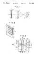
- FIG. 1is a schematic diagram showing a liquid crystal display apparatus as one embodiment of this invention
- FIG. 2is a perspective view of a first embodiment of an optical sheet
- FIG. 3is a schematic diagram showing the arrangement and action of the first embodiment of the optical sheet
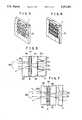
- FIG. 4is a perspective view of a second embodiment of the optical sheet
- FIG. 5is a schematic diagram showing the arrangement and action of the second embodiment of the optical sheet
- FIG. 6is a perspective view of a third embodiment of the optical sheet
- FIG. 7is a schematic diagram showing the arrangement and action of the third embodiment of the optical sheet.
- FIG. 8is a perspective view of a fourth embodiment of the optical sheet
- FIG. 9is a schematic diagram showing the arrangement and action of the fourth embodiment of the optical sheet.
- FIGS. 10 and 11are schematic diagrams showing the arrangements of other optical sheets
- FIG. 12shows one example of a conventional liquid crystal apparatus
- FIG. 13is a schematic diagram showing the structure of an active matrix type liquid cell.
- FIG. 1shows a liquid crystal display apparatus as one embodiment of this invention.
- the components that are identical with those in FIG. 12are given like reference numerals.
- reference symbol Adenotes an optical sheet attached on the back (the light source side) of a liquid crystal cell 8 and represents all the optical sheets 1 to 4 described in each of the succeeding embodiments.
- Illuminating light from a light source 5is reflected by a reflector 6 in the form of a rotating elliptic surface and collimated by a condenser lens 7 before being radiated on the optical sheet A.
- the optical sheet Ais formed of a large number of optical elements, such as convex lenses or prisms, aligned in position with each of picture elements or pixels of the liquid crystal cell 8.
- Each of the optical elementscollects incoming illuminating light onto each corresponding pixel so that the major portion of the light coming from the condenser lens 7 is radiated against the pixels of the liquid crystal cell 8.
- the light that has passed through the pixels onto the front side of the liquid crystal cell 8forms an image on it.
- FIG. 2shows a first embodiment of the optical sheet A and FIG. 3 the arrangement and action of the optical sheet.
- the optical sheet 1is formed of a transparent acrylic material and has on its surface a large number of convex lenses 1a arranged at the same pitches as the pixels of the liquid crystal cell 8. In FIG. 2, only a part of the optical sheet is shown for simplicity.
- the optical sheet 1has convex lenses 1a on the side of the liquid crystal cell 8, with the diameter d of each convex lens 1a set equal to a pitch p.
- a boundary portion B between the adjacent convex lenses 1a 1 and 1a 2is set at a position corresponding to the matrix circuit portion 83 of the liquid crystal cell 8.
- the illuminating light entering each convex lens 1awhich includes rays of light that would otherwise be radiated against the matrix circuit section 83, is focused on the corresponding pixel 88.
- the lightthen passes through a liquid crystal layer 87 and goes out from an opening 85a.
- the illuminating light that would have been radiated against the black matrix layer 85 if the optical sheet 1 was not providedis collected by the convex lens 1a into the pixel.
- Another advantageis that since light is not radiated against the matrix circuit section 83 nor the black matrix layer 85, the liquid crystal cell 8 can be prevented from being heated.
- FIG. 4shows a second embodiment of the optical sheet A, and FIG. 5 its arrangement and action.
- the optical sheet 2 of this embodimentis formed of the same transparent acrylic material as in the first embodiment.
- On the surface of the optical sheet 2are formed a large number of truncated pyramidal prisms 2a arranged at the same pitches as the pixels of the liquid crystal cell 8.
- truncated prismrefers to a prism having opposite planar top and bottom surfaces and side walls by means of which the rays of light from the light source are focused on the corresponding pixel.
- the prisms 2aare directed toward the liquid crystal cell 8 and the boundary portion B between the adjacent prisms 2a 1 and 2a 2 is set at a position corresponding to the matrix circuit section 83.
- those rays that would hit the matrix circuit section 83 if optical elements were not providedare reflected by a side surface 2a A of the prism 2a and gathered from an upper surface 2a 8 into the pixel 88. That is, the illuminating light including the light that corresponds to the matrix circuit section 83 is focused on the pixel 88 by the corresponding prism 2a.
- the light that has passed through the liquid crystal layer 87is thrown out from the openings 85a. Therefore, as with the first embodiment, the illuminating light is effectively utilized to provide a bright image. At the same time, the temperature rise in the liquid crystal cell 8 can be prevented.
- FIG. 6shows a third embodiment of the optical sheet A, and FIG. 7 its arrangement and action.
- the optical sheet 3 of this embodimentis formed of a large number of truncated pyramidal prisms 3a arranged at the same pitches as the pixels, as with the second embodiment.
- the prism 3ais lower in height than the prism 2a of the second embodiment.
- the light entering that part of the prism which corresponds to the matrix circuit section 83is refracted by a side surface 3a A of the prism 3a to be led into the pixel 88, forming a bright image and preventing a temperature rise of the liquid crystal cell 8.
- optical sheets 1 to 3 of the above embodiments with a number of convex or concave elements formed on their surfacemay easily be formed by injection molding or hot pressing of acrylic resin or by performing an ultraviolet ray processing on a photo-form glass.
- FIG. 8shows a fourth embodiment of the optical sheet A and FIG. 9 its arrangement and action.
- the optical sheet 4 of this embodimentconsists of refraction factor distributing type lenses 4a arranged at the same pitches as the pixels of the liquid crystal cell 8 and formed in a glass plate.
- the refraction factor distributing type lens 4amay be formed by an ion exchange technology and a photolithography technology.
- the optical sheet 4 of this embodimentfocuses the light entering that portion of each lens which corresponds to the matrix circuit section 83 on the corresponding pixels 88 by the refraction factor distributing type lens 4a. In this way, the effect similar to that obtained in the preceding embodiments can be produced.
- the optical elementssuch as convex lenses or prisms are directed toward the liquid crystal cell 8. They may, however, be directed toward the light source, like optical elements Aa shown in FIG. 10, or formed into concave lenses as shown in FIG. 11.
- the optical elementsare directed toward the liquid crystal cell 8, it is possible to form a condenser lens integrally on the back (light source side) of the optical sheet as one piece.
- the rays of light from the light sourceare rendered parallel before being thrown into the optical elements, the above-mentioned effect can also be obtained for diffusing or expanding rays of light.
- the liquid crystal cell 8 and the optical sheet Amay be bonded together by bonding agent.
- the preceding embodimentshave the optical elements formed over the entire surface of the screen (over all pixels), they may be provided partly over any desired portion of the screen from which the image is to be enlarged and projected and which therefore requires an increased luminance.
- the liquid crystal display apparatus of FIG. 1has been described to have a single liquid crystal cell, but it is of course applicable also to a liquid crystal projector which has three liquid crystal cells for three colors--red, green and blue--and combines them to form a color image.
- the optical elements disposed opposite to the corresponding pixelsare arranged on the light source side of the liquid crystal cell to focus the light radiated from the light source on each of the pixels. This arrangement enables an effective use of the illuminating light in enhancing the brightness of the image and preventing the temperature rise in the liquid crystal cell.
Landscapes
- Physics & Mathematics (AREA)
- Nonlinear Science (AREA)
- Mathematical Physics (AREA)
- Chemical & Material Sciences (AREA)
- Crystallography & Structural Chemistry (AREA)
- General Physics & Mathematics (AREA)
- Optics & Photonics (AREA)
- Liquid Crystal (AREA)
- Devices For Indicating Variable Information By Combining Individual Elements (AREA)
Abstract
Description
The present invention relates to a liquid crystal display apparatus in which illuminating light is radiated from the back of an active matrix type liquid crystal cell and more particularly to a liquid crystal display apparatus suited for application on a liquid crystal projector.
A conventional liquid crystal display apparatus of this kind has a construction as shown in FIG. 12. In the figure, light from alight source 5 is reflected by a reflector 6 and collimated by acondenser lens 7. The parallel rays of light are then radiated onto the back of an active matrix typeliquid crystal cell 8. The light that passes through theliquid crystal cell 8 forms an image.
FIG. 13 shows the construction of the active matrix typeliquid crystal cell 8.
On aglass substrate 81 are formed transparentpicture cell electrodes 82 or pixel electrodes such as ITO and amatrix circuit section 83 to apply voltage to thesepixel electrodes 82. Thin-film transistors 83T in thematrix circuit section 83 are each connected to thepixel electrodes 82 and also connected with agate line 83G and asource line 83S. On aglass substrate 84 is formed ablack matrix layer 85, which covers thematrix circuit section 83 and hasopenings 85a at portions facing thepixel electrodes 82. Theglass substrate 84 also has acommon electrode 86 formed thereon, such as transparent ITO, which opposes thepixel electrodes 86. Aliquid crystal layer 87 is interposed between thepixel electrodes 82 and thecommon electrode 86. A pixel orpicture element 88 is formed by the opening 85a of theblack matrix layer 85 and thepixel electrode 82. Polarizingplates 89 are attached on the outer sides of theglass substrates
According to image signals applied to thegate line 83G and thesource line 83S, pixel information is written into a capacitance between thepixel electrode 82 and thecommon electrode 86.
In the active matrix typeliquid crystal cell 8, the area of thepixel 88 is equivalent to that of the opening 85a in theblack matrix layer 85, so that the brightness of the image on the conventional display apparatus is determined by the opening factor of the opening 85a. Thus, when the number of pixels is increased, the area occupied by thematrix circuit section 83 also increases, which in turn reduces the opening factor of thepixels 88 and therefore the brightness of the image.
As one of the apparatuses employing the above-mentioned crystal cells, a liquid crystal projector has been developed which projects an enlarged image from the liquid crystal cell onto a screen. In such a projector the liquid crystal cell is required to form an image with high luminance enough to produce an enlarged projected image. The liquid crystal projector, in particular, uses a high-output metal halide lamp as a light source, so that the liquid crystal cell is easily heated by the high-energy light radiated against the matrix circuit section and the black matrix layer. The resulting temperature rise in the liquid crystal cell may degrade its performance.
The present invention has been accomplished with a view to overcoming the above drawback, and its objective is to provide a liquid crystal display apparatus using an active matrix type liquid crystal cell, which makes effective use of illuminating light to suppress a temperature rise in the liquid crystal cells and also increase the brightness of an image.
To achieve the above objective, in the liquid crystal display apparatus of this invention that uses an active matrix type liquid crystal cell and a light source to throw light upon the back of the liquid crystal cell, optical elements are arranged on the light source side of the liquid crystal cell and aligned with pixels to converge light from the light source onto the pixels, thus making effective use of illuminating light in suppressing temperature rise in the liquid crystal cell and increasing the brightness of an image.
FIG. 1 is a schematic diagram showing a liquid crystal display apparatus as one embodiment of this invention;
FIG. 2 is a perspective view of a first embodiment of an optical sheet;
FIG. 3 is a schematic diagram showing the arrangement and action of the first embodiment of the optical sheet;
FIG. 4 is a perspective view of a second embodiment of the optical sheet;
FIG. 5 is a schematic diagram showing the arrangement and action of the second embodiment of the optical sheet;
FIG. 6 is a perspective view of a third embodiment of the optical sheet;
FIG. 7 is a schematic diagram showing the arrangement and action of the third embodiment of the optical sheet;
FIG. 8 is a perspective view of a fourth embodiment of the optical sheet;
FIG. 9 is a schematic diagram showing the arrangement and action of the fourth embodiment of the optical sheet;
FIGS. 10 and 11 are schematic diagrams showing the arrangements of other optical sheets;
FIG. 12 shows one example of a conventional liquid crystal apparatus; and
FIG. 13 is a schematic diagram showing the structure of an active matrix type liquid cell.
FIG. 1 shows a liquid crystal display apparatus as one embodiment of this invention. The components that are identical with those in FIG. 12 are given like reference numerals.
In the figure, reference symbol A denotes an optical sheet attached on the back (the light source side) of aliquid crystal cell 8 and represents all the optical sheets 1 to 4 described in each of the succeeding embodiments.
Illuminating light from alight source 5 is reflected by a reflector 6 in the form of a rotating elliptic surface and collimated by acondenser lens 7 before being radiated on the optical sheet A.
The optical sheet A, as described later, is formed of a large number of optical elements, such as convex lenses or prisms, aligned in position with each of picture elements or pixels of theliquid crystal cell 8. Each of the optical elements collects incoming illuminating light onto each corresponding pixel so that the major portion of the light coming from thecondenser lens 7 is radiated against the pixels of theliquid crystal cell 8. The light that has passed through the pixels onto the front side of theliquid crystal cell 8 forms an image on it.
FIG. 2 shows a first embodiment of the optical sheet A and FIG. 3 the arrangement and action of the optical sheet. The optical sheet 1 is formed of a transparent acrylic material and has on its surface a large number of convex lenses 1a arranged at the same pitches as the pixels of theliquid crystal cell 8. In FIG. 2, only a part of the optical sheet is shown for simplicity.
As shown in FIG. 3, the optical sheet 1 has convex lenses 1a on the side of theliquid crystal cell 8, with the diameter d of each convex lens 1a set equal to a pitch p. A boundary portion B between the adjacent convex lenses 1a1 and 1a2 is set at a position corresponding to thematrix circuit portion 83 of theliquid crystal cell 8. The illuminating light entering each convex lens 1a, which includes rays of light that would otherwise be radiated against thematrix circuit section 83, is focused on thecorresponding pixel 88. The light then passes through aliquid crystal layer 87 and goes out from an opening 85a.
Hence, the illuminating light that would have been radiated against theblack matrix layer 85 if the optical sheet 1 was not provided is collected by the convex lens 1a into the pixel. This makes effective use of the illuminating light, forming a bright image. Another advantage is that since light is not radiated against thematrix circuit section 83 nor theblack matrix layer 85, theliquid crystal cell 8 can be prevented from being heated.
FIG. 4 shows a second embodiment of the optical sheet A, and FIG. 5 its arrangement and action. Theoptical sheet 2 of this embodiment is formed of the same transparent acrylic material as in the first embodiment. On the surface of theoptical sheet 2 are formed a large number of truncatedpyramidal prisms 2a arranged at the same pitches as the pixels of theliquid crystal cell 8. It is noted that the term truncated prism as used herein refers to a prism having opposite planar top and bottom surfaces and side walls by means of which the rays of light from the light source are focused on the corresponding pixel.
As shown in FIG. 5, theprisms 2a are directed toward theliquid crystal cell 8 and the boundary portion B between theadjacent prisms matrix circuit section 83. Of the light rays incident upon eachprism 2a, those rays that would hit thematrix circuit section 83 if optical elements were not provided are reflected by aside surface 2aA of theprism 2a and gathered from anupper surface 2a8 into thepixel 88. That is, the illuminating light including the light that corresponds to thematrix circuit section 83 is focused on thepixel 88 by thecorresponding prism 2a. And the light that has passed through theliquid crystal layer 87 is thrown out from theopenings 85a. Therefore, as with the first embodiment, the illuminating light is effectively utilized to provide a bright image. At the same time, the temperature rise in theliquid crystal cell 8 can be prevented.
FIG. 6 shows a third embodiment of the optical sheet A, and FIG. 7 its arrangement and action. The optical sheet 3 of this embodiment is formed of a large number of truncatedpyramidal prisms 3a arranged at the same pitches as the pixels, as with the second embodiment. Theprism 3a is lower in height than theprism 2a of the second embodiment. The light entering that part of the prism which corresponds to thematrix circuit section 83 is refracted by aside surface 3aA of theprism 3a to be led into thepixel 88, forming a bright image and preventing a temperature rise of theliquid crystal cell 8.
The optical sheets 1 to 3 of the above embodiments with a number of convex or concave elements formed on their surface may easily be formed by injection molding or hot pressing of acrylic resin or by performing an ultraviolet ray processing on a photo-form glass.
FIG. 8 shows a fourth embodiment of the optical sheet A and FIG. 9 its arrangement and action. Theoptical sheet 4 of this embodiment consists of refraction factor distributing type lenses 4a arranged at the same pitches as the pixels of theliquid crystal cell 8 and formed in a glass plate. The refraction factor distributing type lens 4a may be formed by an ion exchange technology and a photolithography technology.
Like the foregoing embodiments, theoptical sheet 4 of this embodiment focuses the light entering that portion of each lens which corresponds to thematrix circuit section 83 on the correspondingpixels 88 by the refraction factor distributing type lens 4a. In this way, the effect similar to that obtained in the preceding embodiments can be produced.
In the foregoing embodiments, the optical elements such as convex lenses or prisms are directed toward theliquid crystal cell 8. They may, however, be directed toward the light source, like optical elements Aa shown in FIG. 10, or formed into concave lenses as shown in FIG. 11. When the optical elements are directed toward theliquid crystal cell 8, it is possible to form a condenser lens integrally on the back (light source side) of the optical sheet as one piece.
While in the above embodiments, the rays of light from the light source are rendered parallel before being thrown into the optical elements, the above-mentioned effect can also be obtained for diffusing or expanding rays of light.
Theliquid crystal cell 8 and the optical sheet A may be bonded together by bonding agent.
Although the preceding embodiments have the optical elements formed over the entire surface of the screen (over all pixels), they may be provided partly over any desired portion of the screen from which the image is to be enlarged and projected and which therefore requires an increased luminance.
The liquid crystal display apparatus of FIG. 1 has been described to have a single liquid crystal cell, but it is of course applicable also to a liquid crystal projector which has three liquid crystal cells for three colors--red, green and blue--and combines them to form a color image.
According to the liquid crystal display apparatus of this invention, the optical elements disposed opposite to the corresponding pixels are arranged on the light source side of the liquid crystal cell to focus the light radiated from the light source on each of the pixels. This arrangement enables an effective use of the illuminating light in enhancing the brightness of the image and preventing the temperature rise in the liquid crystal cell.
Claims (3)
1. A liquid crystal display apparatus comprising:
an active matrix type liquid crystal cell;
a light source to radiate illuminating light onto the back of the liquid crystal cell; and
optical means on the light source side of the liquid crystal cell and disposed close to and facing pixels of the liquid crystal cell, said optical means being adapted to focus the rays of light from the light source on each of the pixels, wherein said optical means includes a transparent optical sheet having on a surface thereof a number of truncated prisms equal to the number of pixels, and wherein each of said prisms is aligned with a respective one of said pixels of the liquid crystal cell.
2. A liquid crystal display apparatus comprising:
an active matrix type liquid crystal cell;
a light source to radiate illuminating light onto the back of the liquid crystal cell; and
optical means on the light source side of the liquid crystal cell and disposed close to and facing pixels of the liquid crystal cell, said optical means being adapted to focus the rays of light from the light source on each of the pixels, wherein said optical means includes a transparent optical sheet having on a surface thereof a number of truncated pyramidal prisms equal to the number of pixels, and wherein each of said prisms is aligned with a respective one of said pixels of the liquid crystal cell.
3. A liquid crystal display apparatus comprising:
an active matrix type liquid crystal cell;
a light source for radiating illuminating light onto the back of the liquid crystal cell; and
optical means on the light source side of the liquid crystal cell and disposed close to and facing the pixels of the liquid crystal cell, said optical means being adapted to focus the rays of light from the light source on each of the pixels, wherein said optical means includes a transparent optical sheet extending substantially over the entire light source side and divided into optical elements of a number corresponding to the number of pixels, each of the optical elements being aligned with a respective one of said pixels of the liquid crystal cell, and having top and bottom planar faces which are parallel with said optical sheet and have at least a portion of the light rays passing directly therethrough onto the pixels and having lateral faces which reflect onto the pixels the remaining portion of the light rays incident on each of optical elements.
Applications Claiming Priority (2)
| Application Number | Priority Date | Filing Date | Title |
|---|---|---|---|
| JP1-308881 | 1989-11-30 | ||
| JP1308881AJPH03170911A (en) | 1989-11-30 | 1989-11-30 | Liquid crystal display device |
Publications (1)
| Publication Number | Publication Date |
|---|---|
| US5151801Atrue US5151801A (en) | 1992-09-29 |
Family
ID=17986386
Family Applications (1)
| Application Number | Title | Priority Date | Filing Date |
|---|---|---|---|
| US07/619,641Expired - Fee RelatedUS5151801A (en) | 1989-11-30 | 1990-11-29 | Liquid crystal display apparatus providing improved illumination via trucated prisms |
Country Status (2)
| Country | Link |
|---|---|
| US (1) | US5151801A (en) |
| JP (1) | JPH03170911A (en) |
Cited By (67)
| Publication number | Priority date | Publication date | Assignee | Title |
|---|---|---|---|---|
| EP0593265A1 (en)* | 1992-10-12 | 1994-04-20 | Sharp Kabushiki Kaisha | Projection apparatus for holographic stereogram recording |
| US5349453A (en)* | 1991-08-23 | 1994-09-20 | Sony Corporation | Liquid crystal display device with microlenses on same plane as switching elements |
| US5359440A (en)* | 1989-10-23 | 1994-10-25 | Sharp Kabushiki Kaisha | Image display apparatus with microlens plate having mutually fused together lenses resulting in hexagonal shaped microlenses |
| US5377027A (en)* | 1992-10-02 | 1994-12-27 | Motorola, Inc. | Liquid crystal display device with pixel registration illumination |
| US5396350A (en)* | 1993-11-05 | 1995-03-07 | Alliedsignal Inc. | Backlighting apparatus employing an array of microprisms |
| DE4332699A1 (en)* | 1993-09-25 | 1995-03-30 | Thomson Brandt Gmbh | Process for increasing the effective opening ratio of liquid crystal light valves |
| US5428468A (en)* | 1993-11-05 | 1995-06-27 | Alliedsignal Inc. | Illumination system employing an array of microprisms |
| US5467208A (en)* | 1992-06-01 | 1995-11-14 | Sharp Kabushiki Kaisha | Liquid crystal display |
| US5481385A (en)* | 1993-07-01 | 1996-01-02 | Alliedsignal Inc. | Direct view display device with array of tapered waveguide on viewer side |
| US5521725A (en)* | 1993-11-05 | 1996-05-28 | Alliedsignal Inc. | Illumination system employing an array of microprisms |
| US5521726A (en)* | 1994-08-26 | 1996-05-28 | Alliedsignal Inc. | Polarizer with an array of tapered waveguides |
| US5555329A (en)* | 1993-11-05 | 1996-09-10 | Alliesignal Inc. | Light directing optical structure |
| US5555476A (en)* | 1993-08-30 | 1996-09-10 | Toray Industries, Inc. | Microlens array sheet for a liquid crystal display, method for attaching the same and liquid crystal display equipped with the same |
| US5581379A (en)* | 1993-02-15 | 1996-12-03 | Omron Corporation | Rectangular based convex microlenses surrounded within a frame and method of making |
| US5598281A (en)* | 1993-11-19 | 1997-01-28 | Alliedsignal Inc. | Backlight assembly for improved illumination employing tapered optical elements |
| US5600456A (en)* | 1994-09-01 | 1997-02-04 | Nec Corporation | Transmission liquid crystal display with a reduced dependency of a display quality upon a visual angle |
| US5631750A (en)* | 1990-11-28 | 1997-05-20 | Canon Kabushiki Kaisha | Scattering type liquid crystal device |
| US5657408A (en)* | 1994-12-23 | 1997-08-12 | Alliedsignal Inc. | Optical device comprising a plurality of units having at least two geometrically-differentiated tapered optical waveguides therein |
| US5666175A (en)* | 1990-12-31 | 1997-09-09 | Kopin Corporation | Optical systems for displays |
| US5680186A (en)* | 1990-02-26 | 1997-10-21 | Sharp Kabushiki Kaisha | Liquid crystal display device with microlenses having a focal point between a cover layer and the liquid crystal layer's center |
| FR2751434A1 (en)* | 1996-07-15 | 1998-01-23 | Lgelectronics | MICROLENCH LIQUID CRYSTAL DISPLAY DEVICE |
| US5875008A (en)* | 1993-10-04 | 1999-02-23 | Matsushita Electric Industrial Co., Ltd. | Liquid crystal panel and projection display with use of liquid crystal panel |
| EP1014158A1 (en)* | 1998-12-22 | 2000-06-28 | Mannesmann VDO Aktiengesellschaft | Display device |
| US6129439A (en)* | 1993-11-05 | 2000-10-10 | Alliedsignal Inc. | Illumination system employing an array of multi-faceted microprisms |
| US6344886B2 (en)* | 1998-09-22 | 2002-02-05 | Stanley Electric Co., Ltd. | Light guide device enhancing a polarized component and liquid crystal display device |
| US6356391B1 (en) | 1999-10-08 | 2002-03-12 | 3M Innovative Properties Company | Optical film with variable angle prisms |
| US6417831B2 (en)* | 1997-03-06 | 2002-07-09 | Dai Nippon Printing Co., Ltd. | Diffused light controlling optical sheet, back light device and liquid crystal display apparatus |
| US6447135B1 (en) | 1999-10-08 | 2002-09-10 | 3M Innovative Properties Company | Lightguide having a directly secured reflector and method of making the same |
| US20030214615A1 (en)* | 2002-05-14 | 2003-11-20 | International Business Machines Corporation | Display panel, liquid crystal display panel, and liquid crystal display device |
| US20040239822A1 (en)* | 2003-03-28 | 2004-12-02 | Seiko Epson Corporation | Space light modulating apparatus, projector including same, process for manufacturing microstructure element used in same, and microstructure element manufactured by same process |
| US20040257496A1 (en)* | 2003-06-20 | 2004-12-23 | Casio Computer Co., Ltd. | Display device and manufacturing method of the same |
| US20050001043A1 (en)* | 1999-10-08 | 2005-01-06 | 3M Innovative Properties Company | Optical elements having programmed optical structures |
| US20050018307A1 (en)* | 2003-07-16 | 2005-01-27 | Seiko Epson Corporation | Spatial light modulator and projector |
| US20060051048A1 (en)* | 1999-10-08 | 2006-03-09 | Gardiner Mark E | Backlight with structured surfaces |
| US20060176540A1 (en)* | 2005-02-07 | 2006-08-10 | Seiko Epson Corporation | Spatial light modulator and image display device |
| EP1818713A1 (en)* | 2006-02-14 | 2007-08-15 | Seiko Epson Corporation | Electro-optic device, method for manufacturing electro-optic device, projector, and electronic apparatus |
| US20070258137A1 (en)* | 2006-05-08 | 2007-11-08 | Seiko Epson Corporation | Electrooptic Device, Electrooptic-Device Substrate, Method for Manufacturing Electrooptic Device, and Projector |
| US20090040426A1 (en)* | 2004-01-20 | 2009-02-12 | Jonathan Mather | Directional backlight, a multiple view display and a multi-direction display |
| US20090086301A1 (en)* | 2004-09-27 | 2009-04-02 | Idc, Llc | Display element having filter material diffused in a substrate of the display element |
| US20090225394A1 (en)* | 2004-09-27 | 2009-09-10 | Idc, Llc | System and method of illuminating interferometric modulators using backlighting |
| US20090231245A1 (en)* | 2008-03-11 | 2009-09-17 | Craig Lin | Luminance enhancement structure for reflective display devices |
| US20090257108A1 (en)* | 2008-04-15 | 2009-10-15 | Qualcomm Mems Technologies, Inc. | Light with bi-directional propagation |
| US20090296194A1 (en)* | 2004-09-27 | 2009-12-03 | Idc, Llc | Optical films for directing light towards active areas of displays |
| US20100141573A1 (en)* | 2008-12-05 | 2010-06-10 | Craig Lin | Luminance enhancement structure with moire reducing design |
| US20100177396A1 (en)* | 2009-01-13 | 2010-07-15 | Craig Lin | Asymmetrical luminance enhancement structure for reflective display devices |
| US20100182351A1 (en)* | 2009-01-22 | 2010-07-22 | Craig Lin | Luminance enhancement structure with varying pitches |
| US20100225999A1 (en)* | 2009-03-09 | 2010-09-09 | Craig Lin | Luminance enhancement structure for reflective display devices |
| US20100271407A1 (en)* | 2009-04-22 | 2010-10-28 | Andrew Ho | Reflective display devices with luminance enhancement film |
| CN101017275B (en)* | 2006-02-06 | 2010-11-17 | 精工爱普生株式会社 | Concentrating substrates, electro-optical devices, substrates for electro-optic devices, projectors, and electronic equipment |
| US20100309103A1 (en)* | 2004-09-27 | 2010-12-09 | Qualcomm Mems Technologies, Inc. | Methods and devices for lighting displays |
| US20110043894A1 (en)* | 2007-11-30 | 2011-02-24 | Sprague Robert A | Display devices having micro-reflectors and color filters |
| US20110057927A1 (en)* | 2008-03-11 | 2011-03-10 | Craig Lin | Luminance enhancement structure for reflective display devices |
| US7933475B2 (en) | 2006-02-17 | 2011-04-26 | Qualcomm Mems Technologies, Inc. | Method and apparatus for providing back-lighting in a display device |
| US20110140155A1 (en)* | 2009-12-16 | 2011-06-16 | Seiko Epson Corporation | Electrooptical device and electronic apparatus |
| US8045252B2 (en) | 2004-02-03 | 2011-10-25 | Qualcomm Mems Technologies, Inc. | Spatial light modulator with integrated optical compensation structure |
| US8172417B2 (en) | 2009-03-06 | 2012-05-08 | Qualcomm Mems Technologies, Inc. | Shaped frontlight reflector for use with display |
| US8237892B1 (en)* | 2007-11-30 | 2012-08-07 | Sipix Imaging, Inc. | Display device with a brightness enhancement structure |
| US8456589B1 (en) | 2009-07-27 | 2013-06-04 | Sipix Imaging, Inc. | Display device assembly |
| US8798425B2 (en) | 2007-12-07 | 2014-08-05 | Qualcomm Mems Technologies, Inc. | Decoupled holographic film and diffuser |
| US8797633B1 (en) | 2009-07-23 | 2014-08-05 | Sipix Imaging, Inc. | Display device assembly and manufacture thereof |
| US8848294B2 (en) | 2010-05-20 | 2014-09-30 | Qualcomm Mems Technologies, Inc. | Method and structure capable of changing color saturation |
| US8872085B2 (en) | 2006-10-06 | 2014-10-28 | Qualcomm Mems Technologies, Inc. | Display device having front illuminator with turning features |
| US8979349B2 (en) | 2009-05-29 | 2015-03-17 | Qualcomm Mems Technologies, Inc. | Illumination devices and methods of fabrication thereof |
| US9019183B2 (en) | 2006-10-06 | 2015-04-28 | Qualcomm Mems Technologies, Inc. | Optical loss structure integrated in an illumination apparatus |
| US9025235B2 (en) | 2002-12-25 | 2015-05-05 | Qualcomm Mems Technologies, Inc. | Optical interference type of color display having optical diffusion layer between substrate and electrode |
| CN106019687A (en)* | 2016-07-12 | 2016-10-12 | 京东方科技集团股份有限公司 | Display panel and display device |
| CN106154633A (en)* | 2016-09-21 | 2016-11-23 | 京东方科技集团股份有限公司 | The manufacture method of display floater, display device and display floater |
Families Citing this family (2)
| Publication number | Priority date | Publication date | Assignee | Title |
|---|---|---|---|---|
| JP2831510B2 (en) | 1991-03-14 | 1998-12-02 | 株式会社日立製作所 | Liquid crystal display element and liquid crystal display device using the same |
| US7768707B2 (en) | 2006-02-06 | 2010-08-03 | Seiko Epson Corporation | Converging substrate, electro-optic device, substrate for electro-optic device, projector, and electronic apparatus |
Citations (10)
| Publication number | Priority date | Publication date | Assignee | Title |
|---|---|---|---|---|
| US4126382A (en)* | 1972-09-22 | 1978-11-21 | Giorgio Barzilai | Operational method for displaying images with liquid-crystal electro-optical devices, and apparatus therefor |
| JPS60201326A (en)* | 1984-03-27 | 1985-10-11 | Citizen Watch Co Ltd | Multi-color liquid crystal display device |
| JPS60241024A (en)* | 1984-05-16 | 1985-11-29 | Seiko Epson Corp | Transmissive color liquid crystal display device |
| JPS6294826A (en)* | 1985-10-22 | 1987-05-01 | Seiko Epson Corp | liquid crystal device |
| US4790632A (en)* | 1986-08-12 | 1988-12-13 | Fuji Photo Film Co., Ltd. | Liquid crystal device having the microlenses in correspondence with the pixel electrodes |
| JPS6435416A (en)* | 1987-07-30 | 1989-02-06 | Matsushita Electric Industrial Co Ltd | Liquid crystal panel |
| US4836652A (en)* | 1986-11-13 | 1989-06-06 | Fuji Photo Film Co., Ltd. | Liquid crystal shutter array having microlenses corresponding to the pixel electrodes |
| JPH01189685A (en)* | 1988-01-26 | 1989-07-28 | Seiko Epson Corp | Liquid crystal light valve and video projector with liquid crystal light valve |
| JPH01222221A (en)* | 1988-03-02 | 1989-09-05 | Seiko Epson Corp | liquid crystal display element |
| US4945348A (en)* | 1987-04-22 | 1990-07-31 | Hitachi Ltd. | Liquid crystal display combined with signal input tablet |
Family Cites Families (3)
| Publication number | Priority date | Publication date | Assignee | Title |
|---|---|---|---|---|
| JPS60165621A (en)* | 1984-02-08 | 1985-08-28 | Nec Corp | Transmission type display element |
| JPS6368814A (en)* | 1986-09-10 | 1988-03-28 | Matsushita Electric Works Ltd | Lighting equipment for liquid crystal display |
| JPH01187502A (en)* | 1988-01-22 | 1989-07-26 | Seiko Epson Corp | Flat lens array and liquid crystal display device equipped with flat lens array |
- 1989
- 1989-11-30JPJP1308881Apatent/JPH03170911A/enactivePending
- 1990
- 1990-11-29USUS07/619,641patent/US5151801A/ennot_activeExpired - Fee Related
Patent Citations (10)
| Publication number | Priority date | Publication date | Assignee | Title |
|---|---|---|---|---|
| US4126382A (en)* | 1972-09-22 | 1978-11-21 | Giorgio Barzilai | Operational method for displaying images with liquid-crystal electro-optical devices, and apparatus therefor |
| JPS60201326A (en)* | 1984-03-27 | 1985-10-11 | Citizen Watch Co Ltd | Multi-color liquid crystal display device |
| JPS60241024A (en)* | 1984-05-16 | 1985-11-29 | Seiko Epson Corp | Transmissive color liquid crystal display device |
| JPS6294826A (en)* | 1985-10-22 | 1987-05-01 | Seiko Epson Corp | liquid crystal device |
| US4790632A (en)* | 1986-08-12 | 1988-12-13 | Fuji Photo Film Co., Ltd. | Liquid crystal device having the microlenses in correspondence with the pixel electrodes |
| US4836652A (en)* | 1986-11-13 | 1989-06-06 | Fuji Photo Film Co., Ltd. | Liquid crystal shutter array having microlenses corresponding to the pixel electrodes |
| US4945348A (en)* | 1987-04-22 | 1990-07-31 | Hitachi Ltd. | Liquid crystal display combined with signal input tablet |
| JPS6435416A (en)* | 1987-07-30 | 1989-02-06 | Matsushita Electric Industrial Co Ltd | Liquid crystal panel |
| JPH01189685A (en)* | 1988-01-26 | 1989-07-28 | Seiko Epson Corp | Liquid crystal light valve and video projector with liquid crystal light valve |
| JPH01222221A (en)* | 1988-03-02 | 1989-09-05 | Seiko Epson Corp | liquid crystal display element |
Non-Patent Citations (2)
| Title |
|---|
| M. Brandon, "Display Device", IBM Technical Disclosure Bulletin, vol. 19, No. 2, Jul. 1976, p. 691. |
| M. Brandon, Display Device , IBM Technical Disclosure Bulletin, vol. 19, No. 2, Jul. 1976, p. 691.* |
Cited By (115)
| Publication number | Priority date | Publication date | Assignee | Title |
|---|---|---|---|---|
| US5359440A (en)* | 1989-10-23 | 1994-10-25 | Sharp Kabushiki Kaisha | Image display apparatus with microlens plate having mutually fused together lenses resulting in hexagonal shaped microlenses |
| US5680186A (en)* | 1990-02-26 | 1997-10-21 | Sharp Kabushiki Kaisha | Liquid crystal display device with microlenses having a focal point between a cover layer and the liquid crystal layer's center |
| US5631750A (en)* | 1990-11-28 | 1997-05-20 | Canon Kabushiki Kaisha | Scattering type liquid crystal device |
| US5666175A (en)* | 1990-12-31 | 1997-09-09 | Kopin Corporation | Optical systems for displays |
| US5349453A (en)* | 1991-08-23 | 1994-09-20 | Sony Corporation | Liquid crystal display device with microlenses on same plane as switching elements |
| US5596429A (en)* | 1992-06-01 | 1997-01-21 | Sharp Kabushiki Kaisha | Liquid crystal display |
| US5467208A (en)* | 1992-06-01 | 1995-11-14 | Sharp Kabushiki Kaisha | Liquid crystal display |
| US5377027A (en)* | 1992-10-02 | 1994-12-27 | Motorola, Inc. | Liquid crystal display device with pixel registration illumination |
| US5504602A (en)* | 1992-10-12 | 1996-04-02 | Sharp Kabushiki Kaisha | LCD including a diffusing screen in a plane where emerging light from one pixel abuts light from adjacent pixels |
| EP0593265A1 (en)* | 1992-10-12 | 1994-04-20 | Sharp Kabushiki Kaisha | Projection apparatus for holographic stereogram recording |
| US5581379A (en)* | 1993-02-15 | 1996-12-03 | Omron Corporation | Rectangular based convex microlenses surrounded within a frame and method of making |
| US5481385A (en)* | 1993-07-01 | 1996-01-02 | Alliedsignal Inc. | Direct view display device with array of tapered waveguide on viewer side |
| US5555476A (en)* | 1993-08-30 | 1996-09-10 | Toray Industries, Inc. | Microlens array sheet for a liquid crystal display, method for attaching the same and liquid crystal display equipped with the same |
| DE4332699A1 (en)* | 1993-09-25 | 1995-03-30 | Thomson Brandt Gmbh | Process for increasing the effective opening ratio of liquid crystal light valves |
| US5875008A (en)* | 1993-10-04 | 1999-02-23 | Matsushita Electric Industrial Co., Ltd. | Liquid crystal panel and projection display with use of liquid crystal panel |
| US5555329A (en)* | 1993-11-05 | 1996-09-10 | Alliesignal Inc. | Light directing optical structure |
| US5428468A (en)* | 1993-11-05 | 1995-06-27 | Alliedsignal Inc. | Illumination system employing an array of microprisms |
| US5396350A (en)* | 1993-11-05 | 1995-03-07 | Alliedsignal Inc. | Backlighting apparatus employing an array of microprisms |
| US5555109A (en)* | 1993-11-05 | 1996-09-10 | Alliedsignal Inc. | Illumination system employing an array of microprisms |
| US5521725A (en)* | 1993-11-05 | 1996-05-28 | Alliedsignal Inc. | Illumination system employing an array of microprisms |
| US6129439A (en)* | 1993-11-05 | 2000-10-10 | Alliedsignal Inc. | Illumination system employing an array of multi-faceted microprisms |
| US5598281A (en)* | 1993-11-19 | 1997-01-28 | Alliedsignal Inc. | Backlight assembly for improved illumination employing tapered optical elements |
| US5521726A (en)* | 1994-08-26 | 1996-05-28 | Alliedsignal Inc. | Polarizer with an array of tapered waveguides |
| US5600456A (en)* | 1994-09-01 | 1997-02-04 | Nec Corporation | Transmission liquid crystal display with a reduced dependency of a display quality upon a visual angle |
| US5657408A (en)* | 1994-12-23 | 1997-08-12 | Alliedsignal Inc. | Optical device comprising a plurality of units having at least two geometrically-differentiated tapered optical waveguides therein |
| FR2751434A1 (en)* | 1996-07-15 | 1998-01-23 | Lgelectronics | MICROLENCH LIQUID CRYSTAL DISPLAY DEVICE |
| US9857621B1 (en)* | 1996-07-15 | 2018-01-02 | Lg Display Co., Ltd. | Display device |
| US11156866B2 (en) | 1996-07-15 | 2021-10-26 | Lg Display Co., Ltd. | Display device |
| US20180157108A1 (en)* | 1996-07-15 | 2018-06-07 | Lg Display Co., Ltd. | Display device |
| US10768472B2 (en)* | 1996-07-15 | 2020-09-08 | Lg Display Co., Ltd. | Display device |
| US6417831B2 (en)* | 1997-03-06 | 2002-07-09 | Dai Nippon Printing Co., Ltd. | Diffused light controlling optical sheet, back light device and liquid crystal display apparatus |
| US6344886B2 (en)* | 1998-09-22 | 2002-02-05 | Stanley Electric Co., Ltd. | Light guide device enhancing a polarized component and liquid crystal display device |
| EP1014158A1 (en)* | 1998-12-22 | 2000-06-28 | Mannesmann VDO Aktiengesellschaft | Display device |
| US20060051048A1 (en)* | 1999-10-08 | 2006-03-09 | Gardiner Mark E | Backlight with structured surfaces |
| US6447135B1 (en) | 1999-10-08 | 2002-09-10 | 3M Innovative Properties Company | Lightguide having a directly secured reflector and method of making the same |
| US6707611B2 (en) | 1999-10-08 | 2004-03-16 | 3M Innovative Properties Company | Optical film with variable angle prisms |
| US7221847B2 (en) | 1999-10-08 | 2007-05-22 | 3M Innovative Properties Company | Optical elements having programmed optical structures |
| US20050001043A1 (en)* | 1999-10-08 | 2005-01-06 | 3M Innovative Properties Company | Optical elements having programmed optical structures |
| US6845212B2 (en) | 1999-10-08 | 2005-01-18 | 3M Innovative Properties Company | Optical element having programmed optical structures |
| US6560026B2 (en) | 1999-10-08 | 2003-05-06 | Mark E. Gardiner | Optical film with variable angle prisms |
| US20080050088A1 (en)* | 1999-10-08 | 2008-02-28 | 3M Innovative Properties Company | Backlight with structured surfaces |
| US7046905B1 (en) | 1999-10-08 | 2006-05-16 | 3M Innovative Properties Company | Blacklight with structured surfaces |
| US6356391B1 (en) | 1999-10-08 | 2002-03-12 | 3M Innovative Properties Company | Optical film with variable angle prisms |
| US7873256B2 (en) | 1999-10-08 | 2011-01-18 | 3M Innovative Properties Company | Backlight with structured surfaces |
| US8588574B2 (en) | 1999-10-08 | 2013-11-19 | 3M Innovative Properties Company | Backlight with structured surfaces |
| US6791639B2 (en)* | 2002-05-14 | 2004-09-14 | International Business Machines Corporation | Direct view display with lenticular lens for improved brightness and wide viewing angle |
| US20030214615A1 (en)* | 2002-05-14 | 2003-11-20 | International Business Machines Corporation | Display panel, liquid crystal display panel, and liquid crystal display device |
| US9025235B2 (en) | 2002-12-25 | 2015-05-05 | Qualcomm Mems Technologies, Inc. | Optical interference type of color display having optical diffusion layer between substrate and electrode |
| US7401926B2 (en) | 2003-03-28 | 2008-07-22 | Seiko Epson Corporation | Space light modulating apparatus, projector including same, process for manufacturing microstructure element used in same, and microstructure element manufactured by the same process |
| EP1533651A4 (en)* | 2003-03-28 | 2007-03-07 | Seiko Epson Corp | SPACE LIGHT MODULATOR, PROJECTOR USING SAME, METHOD FOR MANUFACTURING FINE STRUCTURE ELEMENT USED IN THE MODULATOR, AND FINE STRUCTURE ELEMENT MADE THEREBY |
| US20040239822A1 (en)* | 2003-03-28 | 2004-12-02 | Seiko Epson Corporation | Space light modulating apparatus, projector including same, process for manufacturing microstructure element used in same, and microstructure element manufactured by same process |
| US7242444B2 (en) | 2003-03-28 | 2007-07-10 | Seiko Epson Corporation | Space light modulating apparatus, projector including same, process for manufacturing microstructure element used in same, and microstructure element manufactured by same process |
| US20070236670A1 (en)* | 2003-03-28 | 2007-10-11 | Seiko Epson Corporation | Space light modulating apparatus, projector including same, process for manufacturing microstructure element used in same, and microstructure element manufactured by the same process |
| US7227599B2 (en)* | 2003-06-20 | 2007-06-05 | Casio Computer Co., Ltd. | Display device and manufacturing method of the same |
| US20040257496A1 (en)* | 2003-06-20 | 2004-12-23 | Casio Computer Co., Ltd. | Display device and manufacturing method of the same |
| US7327519B2 (en) | 2003-07-16 | 2008-02-05 | Seiko Epson Corporation | Spatial light modulator and projector |
| US20050018307A1 (en)* | 2003-07-16 | 2005-01-27 | Seiko Epson Corporation | Spatial light modulator and projector |
| US7113341B2 (en)* | 2003-07-16 | 2006-09-26 | Seiko Epson Corporation | Spatial light modulator and projector |
| US20060203349A1 (en)* | 2003-07-16 | 2006-09-14 | Seiko Epson Corporation | Spatial light modulator and projector |
| US20090040426A1 (en)* | 2004-01-20 | 2009-02-12 | Jonathan Mather | Directional backlight, a multiple view display and a multi-direction display |
| US8154686B2 (en)* | 2004-01-20 | 2012-04-10 | Sharp Kabushiki Kaisha | Directional backlight, a multiple view display and a multi-direction display |
| US9019590B2 (en) | 2004-02-03 | 2015-04-28 | Qualcomm Mems Technologies, Inc. | Spatial light modulator with integrated optical compensation structure |
| US8045252B2 (en) | 2004-02-03 | 2011-10-25 | Qualcomm Mems Technologies, Inc. | Spatial light modulator with integrated optical compensation structure |
| US8111445B2 (en) | 2004-02-03 | 2012-02-07 | Qualcomm Mems Technologies, Inc. | Spatial light modulator with integrated optical compensation structure |
| US8344377B2 (en) | 2004-09-27 | 2013-01-01 | Qualcomm Mems Technologies, Inc. | Display element having filter material diffused in a substrate of the display element |
| US20090296194A1 (en)* | 2004-09-27 | 2009-12-03 | Idc, Llc | Optical films for directing light towards active areas of displays |
| US7986451B2 (en)* | 2004-09-27 | 2011-07-26 | Qualcomm Mems Technologies, Inc. | Optical films for directing light towards active areas of displays |
| US20090225394A1 (en)* | 2004-09-27 | 2009-09-10 | Idc, Llc | System and method of illuminating interferometric modulators using backlighting |
| US20090086301A1 (en)* | 2004-09-27 | 2009-04-02 | Idc, Llc | Display element having filter material diffused in a substrate of the display element |
| US20100309103A1 (en)* | 2004-09-27 | 2010-12-09 | Qualcomm Mems Technologies, Inc. | Methods and devices for lighting displays |
| US8040588B2 (en) | 2004-09-27 | 2011-10-18 | Qualcomm Mems Technologies, Inc. | System and method of illuminating interferometric modulators using backlighting |
| US8013831B2 (en) | 2004-09-27 | 2011-09-06 | Qualcomm Mems Technologies, Inc. | Methods and devices for lighting displays |
| US20060176540A1 (en)* | 2005-02-07 | 2006-08-10 | Seiko Epson Corporation | Spatial light modulator and image display device |
| CN100401177C (en)* | 2005-02-07 | 2008-07-09 | 精工爱普生株式会社 | Spatial light modulation device and image display device |
| US7184188B2 (en) | 2005-02-07 | 2007-02-27 | Seiko Epson Corporation | Spatial light modulator and image display device |
| CN101017275B (en)* | 2006-02-06 | 2010-11-17 | 精工爱普生株式会社 | Concentrating substrates, electro-optical devices, substrates for electro-optic devices, projectors, and electronic equipment |
| CN101021629B (en)* | 2006-02-14 | 2010-05-26 | 精工爱普生株式会社 | Electro-optical device, manufacturing method of electro-optical device, projector, and electronic device |
| US7693389B2 (en) | 2006-02-14 | 2010-04-06 | Seiko Epson Corporation | Electro-optic device, method for manufacturing electro-optic device, projector, and electronic apparatus |
| EP1818713A1 (en)* | 2006-02-14 | 2007-08-15 | Seiko Epson Corporation | Electro-optic device, method for manufacturing electro-optic device, projector, and electronic apparatus |
| US20070200975A1 (en)* | 2006-02-14 | 2007-08-30 | Seiko Epson Corporation | Electro-optic device, method for manufacturing electro-optic device, projector, and electronic apparatus |
| US7933475B2 (en) | 2006-02-17 | 2011-04-26 | Qualcomm Mems Technologies, Inc. | Method and apparatus for providing back-lighting in a display device |
| US20070258137A1 (en)* | 2006-05-08 | 2007-11-08 | Seiko Epson Corporation | Electrooptic Device, Electrooptic-Device Substrate, Method for Manufacturing Electrooptic Device, and Projector |
| US9019183B2 (en) | 2006-10-06 | 2015-04-28 | Qualcomm Mems Technologies, Inc. | Optical loss structure integrated in an illumination apparatus |
| US8872085B2 (en) | 2006-10-06 | 2014-10-28 | Qualcomm Mems Technologies, Inc. | Display device having front illuminator with turning features |
| US20110043894A1 (en)* | 2007-11-30 | 2011-02-24 | Sprague Robert A | Display devices having micro-reflectors and color filters |
| US8238021B2 (en) | 2007-11-30 | 2012-08-07 | Sipix Imaging, Inc. | Display devices having micro-reflectors and color filters |
| US8237892B1 (en)* | 2007-11-30 | 2012-08-07 | Sipix Imaging, Inc. | Display device with a brightness enhancement structure |
| US8798425B2 (en) | 2007-12-07 | 2014-08-05 | Qualcomm Mems Technologies, Inc. | Decoupled holographic film and diffuser |
| US20090231245A1 (en)* | 2008-03-11 | 2009-09-17 | Craig Lin | Luminance enhancement structure for reflective display devices |
| US20110057927A1 (en)* | 2008-03-11 | 2011-03-10 | Craig Lin | Luminance enhancement structure for reflective display devices |
| US8395836B2 (en) | 2008-03-11 | 2013-03-12 | Sipix Imaging, Inc. | Luminance enhancement structure for reflective display devices |
| US8437069B2 (en) | 2008-03-11 | 2013-05-07 | Sipix Imaging, Inc. | Luminance enhancement structure for reflective display devices |
| US8049951B2 (en) | 2008-04-15 | 2011-11-01 | Qualcomm Mems Technologies, Inc. | Light with bi-directional propagation |
| US20090257108A1 (en)* | 2008-04-15 | 2009-10-15 | Qualcomm Mems Technologies, Inc. | Light with bi-directional propagation |
| US20100141573A1 (en)* | 2008-12-05 | 2010-06-10 | Craig Lin | Luminance enhancement structure with moire reducing design |
| US8441414B2 (en) | 2008-12-05 | 2013-05-14 | Sipix Imaging, Inc. | Luminance enhancement structure with Moiré reducing design |
| US20100177396A1 (en)* | 2009-01-13 | 2010-07-15 | Craig Lin | Asymmetrical luminance enhancement structure for reflective display devices |
| US9025234B2 (en) | 2009-01-22 | 2015-05-05 | E Ink California, Llc | Luminance enhancement structure with varying pitches |
| US20100182351A1 (en)* | 2009-01-22 | 2010-07-22 | Craig Lin | Luminance enhancement structure with varying pitches |
| US8172417B2 (en) | 2009-03-06 | 2012-05-08 | Qualcomm Mems Technologies, Inc. | Shaped frontlight reflector for use with display |
| US20100225999A1 (en)* | 2009-03-09 | 2010-09-09 | Craig Lin | Luminance enhancement structure for reflective display devices |
| US8120836B2 (en) | 2009-03-09 | 2012-02-21 | Sipix Imaging, Inc. | Luminance enhancement structure for reflective display devices |
| US20100271407A1 (en)* | 2009-04-22 | 2010-10-28 | Andrew Ho | Reflective display devices with luminance enhancement film |
| US8714780B2 (en) | 2009-04-22 | 2014-05-06 | Sipix Imaging, Inc. | Display devices with grooved luminance enhancement film |
| US9121979B2 (en) | 2009-05-29 | 2015-09-01 | Qualcomm Mems Technologies, Inc. | Illumination devices and methods of fabrication thereof |
| US8979349B2 (en) | 2009-05-29 | 2015-03-17 | Qualcomm Mems Technologies, Inc. | Illumination devices and methods of fabrication thereof |
| US8797633B1 (en) | 2009-07-23 | 2014-08-05 | Sipix Imaging, Inc. | Display device assembly and manufacture thereof |
| US8456589B1 (en) | 2009-07-27 | 2013-06-04 | Sipix Imaging, Inc. | Display device assembly |
| US20110140155A1 (en)* | 2009-12-16 | 2011-06-16 | Seiko Epson Corporation | Electrooptical device and electronic apparatus |
| US8860054B2 (en)* | 2009-12-16 | 2014-10-14 | Seiko Epson Corporation | Electrooptical device and electronic apparatus |
| US8848294B2 (en) | 2010-05-20 | 2014-09-30 | Qualcomm Mems Technologies, Inc. | Method and structure capable of changing color saturation |
| CN106019687A (en)* | 2016-07-12 | 2016-10-12 | 京东方科技集团股份有限公司 | Display panel and display device |
| CN106019687B (en)* | 2016-07-12 | 2019-08-13 | 京东方科技集团股份有限公司 | A kind of display panel and display device |
| CN106154633A (en)* | 2016-09-21 | 2016-11-23 | 京东方科技集团股份有限公司 | The manufacture method of display floater, display device and display floater |
| US10281763B2 (en) | 2016-09-21 | 2019-05-07 | Boe Technology Group Co., Ltd. | Display panel, display apparatus and manufacturing method of display panel |
Also Published As
| Publication number | Publication date |
|---|---|
| JPH03170911A (en) | 1991-07-24 |
Similar Documents
| Publication | Publication Date | Title |
|---|---|---|
| US5151801A (en) | Liquid crystal display apparatus providing improved illumination via trucated prisms | |
| US7321349B2 (en) | Display element, display device, and microlens array | |
| US5101279A (en) | Liquid crystal display apparatus having lenticular elements oriented in relation to LC pixel aperture dimensions | |
| KR101286095B1 (en) | One-body multi optical sheet for liquid crystal display device | |
| US5757341A (en) | Color liquid crystal projection display systems | |
| WO2005093500A1 (en) | Display panel and method for manufacturing same | |
| US5150138A (en) | Projection type image display apparatus | |
| JPH1096910A (en) | Liquid crystal display device having micro lenses | |
| US5764323A (en) | Transmission type display device with aspheric microlenses | |
| US5430562A (en) | Liquid crystal light valve including between light and light valve microlenses and two reflecting layers with a matrix of openings | |
| JP4583498B2 (en) | Optical member unit, illumination device for display device, display device, and television receiver | |
| JPH03136004A (en) | image display device | |
| KR100582926B1 (en) | Backlight Unit for Liquid Crystal Display | |
| JPH1164836A (en) | Image display device | |
| JP2883430B2 (en) | Liquid crystal display | |
| JPH04251221A (en) | Liquid crystal display device and projection display device using the same | |
| JP3189772B2 (en) | Reflective projection type image display | |
| JPH10253801A (en) | Optical element, liquid crystal display unit and liquid crystal projector | |
| KR100641630B1 (en) | Transmissive Reflective Liquid Crystal Display | |
| JP3223534B2 (en) | Projection display device | |
| JPH06222355A (en) | Light valve device and display device using the device | |
| JP2002148617A (en) | Liquid crystal display | |
| JPH10268786A (en) | Flat panel display | |
| JP2002131742A (en) | Reflection type liquid crystal display device | |
| US6088076A (en) | Liquid crystal display apparatus using holographic optical element |
Legal Events
| Date | Code | Title | Description |
|---|---|---|---|
| AS | Assignment | Owner name:PIONEER ELECTRONIC CORPORATION, 4-1, MEGURO 1-CHOM Free format text:ASSIGNMENT OF ASSIGNORS INTEREST.;ASSIGNOR:HIROSHIMA, YASUNORI;REEL/FRAME:005574/0998 Effective date:19901212 | |
| FEPP | Fee payment procedure | Free format text:PAYOR NUMBER ASSIGNED (ORIGINAL EVENT CODE: ASPN); ENTITY STATUS OF PATENT OWNER: LARGE ENTITY | |
| REMI | Maintenance fee reminder mailed | ||
| LAPS | Lapse for failure to pay maintenance fees | ||
| FP | Lapsed due to failure to pay maintenance fee | Effective date:19961002 | |
| STCH | Information on status: patent discontinuation | Free format text:PATENT EXPIRED DUE TO NONPAYMENT OF MAINTENANCE FEES UNDER 37 CFR 1.362 |