US5151039A - Integrated circuit adapter having gullwing-shaped leads - Google Patents
Integrated circuit adapter having gullwing-shaped leadsDownload PDFInfo
- Publication number
- US5151039A US5151039AUS07/693,446US69344691AUS5151039AUS 5151039 AUS5151039 AUS 5151039AUS 69344691 AUS69344691 AUS 69344691AUS 5151039 AUS5151039 AUS 5151039A
- Authority
- US
- United States
- Prior art keywords
- adapter
- leads
- attachment sites
- connector
- electrical
- Prior art date
- Legal status (The legal status is an assumption and is not a legal conclusion. Google has not performed a legal analysis and makes no representation as to the accuracy of the status listed.)
- Expired - Fee Related
Links
Images


Classifications
- H—ELECTRICITY
- H01—ELECTRIC ELEMENTS
- H01L—SEMICONDUCTOR DEVICES NOT COVERED BY CLASS H10
- H01L21/00—Processes or apparatus adapted for the manufacture or treatment of semiconductor or solid state devices or of parts thereof
- H01L21/67—Apparatus specially adapted for handling semiconductor or electric solid state devices during manufacture or treatment thereof; Apparatus specially adapted for handling wafers during manufacture or treatment of semiconductor or electric solid state devices or components ; Apparatus not specifically provided for elsewhere
- H01L21/67005—Apparatus not specifically provided for elsewhere
- H01L21/67011—Apparatus for manufacture or treatment
- H01L21/67121—Apparatus for making assemblies not otherwise provided for, e.g. package constructions
- H—ELECTRICITY
- H01—ELECTRIC ELEMENTS
- H01R—ELECTRICALLY-CONDUCTIVE CONNECTIONS; STRUCTURAL ASSOCIATIONS OF A PLURALITY OF MUTUALLY-INSULATED ELECTRICAL CONNECTING ELEMENTS; COUPLING DEVICES; CURRENT COLLECTORS
- H01R12/00—Structural associations of a plurality of mutually-insulated electrical connecting elements, specially adapted for printed circuits, e.g. printed circuit boards [PCB], flat or ribbon cables, or like generally planar structures, e.g. terminal strips, terminal blocks; Coupling devices specially adapted for printed circuits, flat or ribbon cables, or like generally planar structures; Terminals specially adapted for contact with, or insertion into, printed circuits, flat or ribbon cables, or like generally planar structures
- H01R12/70—Coupling devices
- H01R12/71—Coupling devices for rigid printing circuits or like structures
- H01R12/712—Coupling devices for rigid printing circuits or like structures co-operating with the surface of the printed circuit or with a coupling device exclusively provided on the surface of the printed circuit
- H01R12/716—Coupling device provided on the PCB
- H—ELECTRICITY
- H05—ELECTRIC TECHNIQUES NOT OTHERWISE PROVIDED FOR
- H05K—PRINTED CIRCUITS; CASINGS OR CONSTRUCTIONAL DETAILS OF ELECTRIC APPARATUS; MANUFACTURE OF ASSEMBLAGES OF ELECTRICAL COMPONENTS
- H05K7/00—Constructional details common to different types of electric apparatus
- H05K7/02—Arrangements of circuit components or wiring on supporting structure
- H05K7/10—Plug-in assemblages of components, e.g. IC sockets
- H05K7/1015—Plug-in assemblages of components, e.g. IC sockets having exterior leads
- H05K7/1023—Plug-in assemblages of components, e.g. IC sockets having exterior leads co-operating by abutting, e.g. flat pack
- H—ELECTRICITY
- H05—ELECTRIC TECHNIQUES NOT OTHERWISE PROVIDED FOR
- H05K—PRINTED CIRCUITS; CASINGS OR CONSTRUCTIONAL DETAILS OF ELECTRIC APPARATUS; MANUFACTURE OF ASSEMBLAGES OF ELECTRICAL COMPONENTS
- H05K7/00—Constructional details common to different types of electric apparatus
- H05K7/02—Arrangements of circuit components or wiring on supporting structure
- H05K7/10—Plug-in assemblages of components, e.g. IC sockets
- H05K7/1053—Plug-in assemblages of components, e.g. IC sockets having interior leads
- H05K7/1076—Plug-in assemblages of components, e.g. IC sockets having interior leads co-operating by sliding
- H05K7/1084—Plug-in assemblages of components, e.g. IC sockets having interior leads co-operating by sliding pin grid array package carriers
Definitions
- This inventionrelates to adapters for interfacing integrated circuits with sockets and printed circuit boards.
- Printed circuit cardsgenerally include plated holes or pads for receiving the leads of an electronic device such as an integrated circuit.
- Surface mounted devicesare mounted on pads on the circuit board and soldered in place.
- Quad flat pack (QFP) devicesinclude gullwing-shaped leads which project out from four sides of a rectangular package and are soldered to four corresponding rows of pads on the circuit board.
- the inventionfeatures an adapter which may connect device leads to contacts, such as pads, arranged in a rectangle on a circuit surface.
- the adapterhas a body and leads that extend outwardly, downwardly and then outwardly again in a pair of opposing curves to form feet which match the pattern on the circuit surface.
- the bodyhas sites for making connections with the device and supports conductive elements which connect the leads to the sites.
- the inventionalso features an adapter which may connect gullwing-shaped device leads disposed in a rectangle to contacts on a circuit surface in a similar pattern.
- the adapterhas a body with contacts matching the device lead pattern for making connections to the device leads, and leads for making electrical connections to the circuit surface, which extend outwardly, downwardly, and then outwardly again in a pair of opposing curves to form feet that match the circuit surface pattern.
- the bodyis a substrate supporting the conductive elements, such as a printed circuit board; leads are connected to it only by soldering to the outer periphery of its upper surface; the conductive elements and adapter leads are portions of a lead frame and the body is molded around them; a connector connected to the attachment sites makes connections to the device leads; this connector is a separate body; this connector includes socket terminals; this connector mates with another connector which has conductive elements for making connections between it and attachment sites on the second body; the second connector includes connector elements supported in a second body; this second body is separate; attachment sites on the second body are contact pads for making solder connections to the leads of the device; a strain relief element on the adapter allows mechanical connection to the circuit surface; the second body is a printed circuit board; portions of a lead frame form the conductive elements which are molded in the second body; the body includes a stack of connected body portions; an upper portion supports the contacts, leads extend from a lower portion, and the adapter includes separable connectors between them; the adapter
- the inventionalso features a method of manufacturing an adapter for removably connecting leads of a device to contacts on a circuit surface arranged in a pattern having four rows, one on each side of a rectangular pattern.
- the methodincludes the steps of molding a first insulating body, sealing a series of leads in a lead frame to the body, and bending the sealed leads into a gullwing shape corresponding to the pattern.
- the step of sealing the leadsis performed by heat sealing the lead frames in grooves molded in the body; the step of sealing the leads is performed by means of an adhesive; terminals are embedded in the body, and are electrically connected to the leads; the step of electrically connecting the leads to the terminals is performed by soldering; the step of electrically connecting the leads to the terminals is performed by pressfitting; a second shot molding portion may be molded around the body and sealed leads.
- the inventionalso features an adapter that is to be connected to contacts on a mother circuit surface.
- the adapterhas a circuit bearing element with connection sites that are connected to metalized holes opening onto its top side. Leads are anchored in the holes and bent down around the edge of the top side of the circuit bearing element to below it, and may be connected to the contacts on the mother circuit surface.
- the inventionalso features a method of providing gullwing-shaped leads to a circuit bearing element, in which lead frame elements are provided in a lead frame.
- the methodincludes bending the lead frame elements into a hook-shape, soldering them in holes in the circuit bearing element, bending the soldered leads down around the edge of the top surface of the circuit bearing element and below it, and removing a side frame portion from the bent lead frame.
- the leadsare lead frame elements; the circuit bearing element is a printed circuit board; the leads are soldered to the holes in the circuit bearing element; the leads are bent outwardly below the circuit bearing element to form feet for attachment to the circuit surface; the leads are bent in a gullwing shape with two opposing curves; receptacles are connected to the connection sites and a chimney provides a mounting for the receptacles; a through-hole pin reinforces the mechanical connection between the adapter and the circuit surface; the contacts are arranged in a pattern having four rows of contacts; one row on each side of a rectangular pattern; the corners of the soldered lead frame are removed before the step of bending the soldered leads; the step of removing a side portion from the bent lead frame is performed after the step of bending the soldered leads; the bending operations are performed with bending tools; the steps of bending the soldered leads and cutting the leads are performed in a single operation with a single tool.
- An adapter according to the inventionallows devices to be interfaced in a variety of ways to a printed circuit board having a gullwing pad configuration.
- a designermay create a single circuit board which can accept a socket in a prototype or upgradable configuration or a soldered-in device for larger-scale, less expensive production.
- the designermay also use sockets on boards that were designed with a simple gullwing pad configuration-- usually an expensive and time-consuming undertaking.
- the designermay even interface different device footprints to a gullwing pad configuration if they are more readily available or include other desireable features.
- a method of providing leads according to the inventionhas the advantage of yielding leads that are solidly anchored in plated holes in a circuit bearing element such as a circuit board.
- a single operationis sufficient to install all of the leads at once, and another single operation bends and cuts all of the leads. Because the leads are bent from the top of the circuit bearing element, the leads are useable with sockets that make contact with the inner surface of the leads, such as those shown in my co-pending application entitled "Integrated Circuit Socket with Reed-Shaped Leads", Ser. No. 616,180, filed Nov. 20, 1990.
- FIG. 1presents a disassembled side view of an adapter, including the device to be mounted thereon as well as the circuit surface onto which the adapter is to be loaded.
- FIG. 2shows a side view of an adapter mounted on a circuit surface with its associated device.
- FIG. 3presents a disassembled side view of another adapter, including the device to be mounted thereon as well as the circuit surface onto which the adapter is to be loaded.
- FIG. 4presents an assembled side view of the adapter, device and ,circuit surface of FIG. 3.
- FIGS. 5-10 and 10ashow manufacturing steps for the gullwing-shaped leads.
- FIG. 11is a partially sectioned side elevation of an adapter with sealed-in leads that is mounted on a circuit surface with its associated device.
- FIG. 12is a plan view of the bottom surface of the chimney connector body.
- FIG. 13is a plan view of a lead frame for use with the chimney connector body of FIG. 13.
- FIGS. 14a and 14binclude two sub-figures of a partial cross-section of the chimney connector body as indicated by the arrows in FIG. 12, showing the leads before and after heat is applied to secure them to the chimney connector body.
- FIG. 15shows a partially sectioned elevation of an adapter according to the invention.
- FIG. 16is a top plan view of a lead frame prior to assembly in the adapter of FIG. 15.
- FIG. 17is a cross-section of the lead frame of FIG. 16 along 17--17, before the bending operations.
- FIG. 18presents the view of FIG. 17 after the first bending operation.
- FIG. 19presents the view of FIG. 17 after the lead frame has been soldered to its printed circuit board element and its corners have been removed.
- FIG. 20presents the view of FIG. 17 after the second bending operation, and shows the removal of the frame portions of the lead frame.
- FIG. 21shows a schematic cross section of a bending apparatus for use in the second bending and cutting operations.
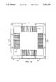
- a QFP device 10may be soldered by its leads 12 to a QFP adapter 14.
- the QFP adapter 14comprises a QFP adapter printed circuit board 18, pads 16 which are placed to correspond to the device leads, and pins 20.
- the QFP adapter printed circuit board 18may be manufactured by printed circuit board fabrication techniques.
- the pins 20are press fit into plated-through holes therein and thus connected to the pads 16 by conductive elements (e.g., traces) in the insulative body of the QFP adapter circuit board.
- the pins 20may also be soldered to the QFP adapter printed circuit board 18.
- the pins 20 of the QFP adapter 14are spaced to engage terminals 24 in chimney connector 22.
- Chimney connector 22is fabricated of insulative material such as glass epoxy or molding compounds, and the terminals 24 are low insertion force socket terminals.
- the terminals 24include solder tails 25 which are soldered to electrical attachment sites on adapter substrate 28.
- Adapter substrate 28may also be manufactured by printed circuit board fabrication techniques.
- Also soldered to the adapter substrate 28are gullwing-shaped adapter leads 26. These gullwing-shaped adapter leads are electrically connected to the electrical attachment sites by conductive elements supported by the insulative body of the adapter substrate 28.
- the gullwing-shaped adapter leads 26are manufactured from a single lead frame 50 which is soldered to the top surface of adapter substrate 28.
- the corners 52 of lead frame 50are then removed (FIG. 6).
- a jig(not shown) is then pressed onto the top of leads 26 to hold them firmly to adapter substrate 28, and the leads are bent in two different directions to form the opposing curves of a gullwing shape (FIGS. 7 and 8).
- the jigprevents the solder joints from being subjected to excessive stress during the bending operation.
- the remainder of the edges 54 of the lead frame 50are then cut (FIG. 9) to form the final gullwing-shaped adapter leads 26 (FIG. 10).
- Leads 26thus include feet adapted to be soldered to standard QFP spaced pads 31 on circuit board surface 30 by the end user with surface mount soldering techniques, as shown in FIG. 2.
- Strain relief elements 32may optionally be mounted on the adapter substrate and soldered to the circuit board 31. The strain relief elements may be soldered in holes in the circuit surface as shown in FIG. 2, or shorter strain relief elements may be soldered to pads on the circuit surface.
- the usermay insert the QFP adapter 14 with a device 10 soldered to it.
- the QFP adapter boardmay be removed 5 from chimney connector 22 and replaced with another adapter board carrying another device.
- an adapteris presented which is configured to receive a device 10 in a socket 38.
- Quad flat pack socketsas shown are available from sources such as AMP or 3M.
- the socket 38includes pins 40 which may be inserted in receptacles 36 in the socket adapter 34.
- the socket adapter 34is made up of a socket adapter circuit board 37 which includes pins 20 which are connected to the receptacles 36 by traces in the socket adapter circuit board. Pins 20 are adapted to engage the terminals 24 in the chimney connector 22.
- the usermay insert the socket adapter 34 into the chimney connector 22.
- a device 10may then be inserted into the socket 38.
- the device 10may be removed from socket 38 and replaced with another device.
- socket adapter 34can be made to have the same pin configuration as the QFP adapter 14 thus making the parts interchangeable on the same chimney connector 22.
- the socket adapter 34may be directly soldered to the adapter substrate 28 by means of pins 20.
- the receptacles 36should be prevented from touching adapter leads 26 (e.g., by using standoffs). This results in a simpler adapter with a lower profile (not shown).
- the socket 38may be a QFP socket, or it may accommodate other device types, such as LCC, PLCC or PGA packages, for example.
- the parts of the adapter that are implemented with printed circuit boardsmay be built using embedded lead frames as discussed in my co-pending application, entitled “Molded-in Lead Frames", Ser. Nos. 121,568 and 272,074, which are herein incorporated by reference.
- the lead frame 50 which is manipulated to form the gullwing-shaped adapter leadsmay also serve to form conductive elements within the adapter substrate. Such a construction would be less expensive to manufacture than those in which the conductive elements are traces formed using printed circuit board fabrication methods.
- the adaptermay also be implemented using the molding process discussed in my application entitled “Molded Integrated Circuit Package", Ser. No. 07/564,406, which is herein incorporated by reference.
- the structure of an adapter made using this methodincludes a plastic molded chimney connector 60 that accepts a QFP adapter 14 and its associated device. Leads are mounted on the lower surface of the plastic molded chimney connector and connected to the terminals 68 within the chimney.
- a plastic chimney connector body 61is first molded in a first-shot molding process. As shown in FIG. 12, on the bottom of the body are grooves 62 that each extend from the edge of the body to the bottom of a hole for holding one of the terminals. At the hole, the channel forms an eye-shaped area 64 around the bottom aperture of the hole.
- Chimney body 61is made by injection-molding a high molding pressure plastic, glass-filled polyphenylene sulfide (PPS).
- PPSpolyphenylene sulfide
- This plasticresists the high temperatures present in wave soldering, vapor phase soldering and infra-red soldering. It also has a low affinity for moisture and desirable dielectric properties.
- This plasticmust be molded at high pressures and temperatures, but the molding operation may be relatively short in duration (e.g., around 15 seconds).
- a typical molding pressureis between 500 and 800 p.s.i.g.
- an associated lead frame 74is then placed on the bottom surface of the body so that each individual lead 76 rests in its corresponding channel 62. It will be observed that eye-shaped portions 75 of the leads will rest in their corresponding eye-shaped areas 64. Referring to FIG. 14a, it can be seen that the ridges 63 between the grooves 62 are thicker than the leads 76 themselves.
- FIG. 14bshows the first-shot portion of the body after the second operation.
- the second operationinvolves the application of heat to the areas between the grooves by pressing on the first-shot portion using a hot metal iron. This application of heat softens the plastic and causes it to surround the leads and thus secure them to the first-shot portion. Since the ridges between the grooves extend beyond the lead frame, there will be a small amount of excess material that will be pressed so as to fill the small voids between the leads and the walls of the grooves.
- the ironis held at a temperature between 425 and 450 degrees fahrenheit, and applied to the chimney connector body with a force of 30 p.s.i.g.
- the terminals 68may be installed in the chimney and connected to the eyes 75 of the leads 76.
- the electrical connectionmay be made by soldering or press-fitting, for example.
- the lead framemay then be cut and bent to leave the gullwing-shaped leads. This may require applying a force to hold the leads in place during the bending operation.
- a QFP adapter 110includes a circuit bearing element, such as a printed circuit board element 112, with plated, or otherwise metalized, holes 113 that accept bent gullwing-shaped leads 114. These leads are soldered to the circuit board element at one end and include feet at the other end which may be soldered to pads arranged in four rows on a mother circuit board 116 or mounted in a suitable socket (not shown). Other interconnect elements, such as receptacles 118 embedded in chimney 119 are also connected to the circuit board element 112 and allow for connection to external circuitry.
- a lead frame 120 for use in assembling an adapter according to the inventionincludes a frame portion 122 and lead elements 124.
- the lead framemay be made by stamping or etching or by any other suitable method.
- the lead elements 124 of the lead frameare first bent (FIG. 18) to a hook-shape in a bending apparatus. Once bent, the lead frame ends are inserted in corresponding holes in the printed circuit board 112, and the lead elements are anchored in place, for example, by infra-red soldering (FIG. 19). With the lead frame soldered in place, its corners 123 (FIG. 16) are cut away. The leads are then bent to their final gullwing shape (FIG. 20) in a second bending operation and the remaining side frame portions 121 (FIG. 16) are cut away.
- the second bending operation and the cutting operationmay be performed in a single operation using a bending apparatus.
- the soldered but unfinished adapter 110is placed on a pedestal 130, and the bending tool 140 is lowered onto the part.
- a spring-loaded jaw 132first engages the adapter and holds it in place on its pedestal.
- four bending implements 136engage the leads and bend them around bending dies 142 on the pedestal. These dies are designed to guide the leads down around the edges of the top of the printed circuit element and impart them with the opposing curves and feet of a gullwing shape.
- the above manufacturing processhas the advantage of performing several steps in a single operation with a single tool. It is, of course, possible to separate the cutting and bending operations into separate individual operations.
- the unfinished adapteris now ready for further operations, such as the addition of a chimney 119 and embedded receptacles as shown in FIG. 15.
- These receptaclesmay be electrically connected to attachment sites on the printed circuit element. These sites are connected to the leads by circuit elements, such as copper traces within the printed circuit element, thus providing connections between the receptacles and the leads.
- Through-hole-type pinsmay also be provided on the adapter, for the purpose of reinforcing the mechanical connection between the adapter and the mother circuit board, when soldered in place.
- Ceramic quad flat pack devicesmay be used with this invention as well as plastic quad flat pack devices (PQFP).
Landscapes
- Engineering & Computer Science (AREA)
- Microelectronics & Electronic Packaging (AREA)
- Physics & Mathematics (AREA)
- Condensed Matter Physics & Semiconductors (AREA)
- General Physics & Mathematics (AREA)
- Manufacturing & Machinery (AREA)
- Computer Hardware Design (AREA)
- Power Engineering (AREA)
- Coupling Device And Connection With Printed Circuit (AREA)
Abstract
Description
This is a continuation-in-part of copending application Ser. No. 07/505,733 filed on Apr. 6, 1990 abandoned.
This invention relates to adapters for interfacing integrated circuits with sockets and printed circuit boards.
Electronic circuits are often built using printed circuit technology. Printed circuit cards generally include plated holes or pads for receiving the leads of an electronic device such as an integrated circuit. Surface mounted devices are mounted on pads on the circuit board and soldered in place. Quad flat pack (QFP) devices include gullwing-shaped leads which project out from four sides of a rectangular package and are soldered to four corresponding rows of pads on the circuit board.
It is known to solder a socket to a printed circuit board to receive a device, thus providing a removable mounting site and electrical connection to the circuit board. Examples of such sockets are presented in Advanced Interconnections Catalog No. 9, (available from 5 Energy Way, West Warwick, RI 02893).
In general, the invention features an adapter which may connect device leads to contacts, such as pads, arranged in a rectangle on a circuit surface. The adapter has a body and leads that extend outwardly, downwardly and then outwardly again in a pair of opposing curves to form feet which match the pattern on the circuit surface. The body has sites for making connections with the device and supports conductive elements which connect the leads to the sites.
In general, the invention also features an adapter which may connect gullwing-shaped device leads disposed in a rectangle to contacts on a circuit surface in a similar pattern. The adapter has a body with contacts matching the device lead pattern for making connections to the device leads, and leads for making electrical connections to the circuit surface, which extend outwardly, downwardly, and then outwardly again in a pair of opposing curves to form feet that match the circuit surface pattern.
In preferred embodiments, the body is a substrate supporting the conductive elements, such as a printed circuit board; leads are connected to it only by soldering to the outer periphery of its upper surface; the conductive elements and adapter leads are portions of a lead frame and the body is molded around them; a connector connected to the attachment sites makes connections to the device leads; this connector is a separate body; this connector includes socket terminals; this connector mates with another connector which has conductive elements for making connections between it and attachment sites on the second body; the second connector includes connector elements supported in a second body; this second body is separate; attachment sites on the second body are contact pads for making solder connections to the leads of the device; a strain relief element on the adapter allows mechanical connection to the circuit surface; the second body is a printed circuit board; portions of a lead frame form the conductive elements which are molded in the second body; the body includes a stack of connected body portions; an upper portion supports the contacts, leads extend from a lower portion, and the adapter includes separable connectors between them; the adapter is made by soldering leads to the periphery of the upper surface of the circuit board, pressing the leads to the board, and bending them into a gullwing shape; the device is a QFP device.
In general, the invention also features a method of manufacturing an adapter for removably connecting leads of a device to contacts on a circuit surface arranged in a pattern having four rows, one on each side of a rectangular pattern. The method includes the steps of molding a first insulating body, sealing a series of leads in a lead frame to the body, and bending the sealed leads into a gullwing shape corresponding to the pattern.
In preferred embodiments, the step of sealing the leads is performed by heat sealing the lead frames in grooves molded in the body; the step of sealing the leads is performed by means of an adhesive; terminals are embedded in the body, and are electrically connected to the leads; the step of electrically connecting the leads to the terminals is performed by soldering; the step of electrically connecting the leads to the terminals is performed by pressfitting; a second shot molding portion may be molded around the body and sealed leads.
In general, the invention also features an adapter that is to be connected to contacts on a mother circuit surface. The adapter has a circuit bearing element with connection sites that are connected to metalized holes opening onto its top side. Leads are anchored in the holes and bent down around the edge of the top side of the circuit bearing element to below it, and may be connected to the contacts on the mother circuit surface.
In general, the invention also features a method of providing gullwing-shaped leads to a circuit bearing element, in which lead frame elements are provided in a lead frame. The method includes bending the lead frame elements into a hook-shape, soldering them in holes in the circuit bearing element, bending the soldered leads down around the edge of the top surface of the circuit bearing element and below it, and removing a side frame portion from the bent lead frame.
In preferred embodiments, the leads are lead frame elements; the circuit bearing element is a printed circuit board; the leads are soldered to the holes in the circuit bearing element; the leads are bent outwardly below the circuit bearing element to form feet for attachment to the circuit surface; the leads are bent in a gullwing shape with two opposing curves; receptacles are connected to the connection sites and a chimney provides a mounting for the receptacles; a through-hole pin reinforces the mechanical connection between the adapter and the circuit surface; the contacts are arranged in a pattern having four rows of contacts; one row on each side of a rectangular pattern; the corners of the soldered lead frame are removed before the step of bending the soldered leads; the step of removing a side portion from the bent lead frame is performed after the step of bending the soldered leads; the bending operations are performed with bending tools; the steps of bending the soldered leads and cutting the leads are performed in a single operation with a single tool.
An adapter according to the invention allows devices to be interfaced in a variety of ways to a printed circuit board having a gullwing pad configuration. For example, a designer may create a single circuit board which can accept a socket in a prototype or upgradable configuration or a soldered-in device for larger-scale, less expensive production. The designer may also use sockets on boards that were designed with a simple gullwing pad configuration-- usually an expensive and time-consuming undertaking. The designer may even interface different device footprints to a gullwing pad configuration if they are more readily available or include other desireable features.
A method of providing leads according to the invention has the advantage of yielding leads that are solidly anchored in plated holes in a circuit bearing element such as a circuit board. A single operation is sufficient to install all of the leads at once, and another single operation bends and cuts all of the leads. Because the leads are bent from the top of the circuit bearing element, the leads are useable with sockets that make contact with the inner surface of the leads, such as those shown in my co-pending application entitled "Integrated Circuit Socket with Reed-Shaped Leads", Ser. No. 616,180, filed Nov. 20, 1990.
We first briefly describe the drawings.
FIG. 1 presents a disassembled side view of an adapter, including the device to be mounted thereon as well as the circuit surface onto which the adapter is to be loaded.
FIG. 2 shows a side view of an adapter mounted on a circuit surface with its associated device.
FIG. 3 presents a disassembled side view of another adapter, including the device to be mounted thereon as well as the circuit surface onto which the adapter is to be loaded.
FIG. 4 presents an assembled side view of the adapter, device and ,circuit surface of FIG. 3.
FIGS. 5-10 and 10a show manufacturing steps for the gullwing-shaped leads.
FIG. 11 is a partially sectioned side elevation of an adapter with sealed-in leads that is mounted on a circuit surface with its associated device.
FIG. 12 is a plan view of the bottom surface of the chimney connector body.
FIG. 13 is a plan view of a lead frame for use with the chimney connector body of FIG. 13.
FIGS. 14a and 14b include two sub-figures of a partial cross-section of the chimney connector body as indicated by the arrows in FIG. 12, showing the leads before and after heat is applied to secure them to the chimney connector body.
FIG. 15 shows a partially sectioned elevation of an adapter according to the invention.
FIG. 16 is a top plan view of a lead frame prior to assembly in the adapter of FIG. 15.
FIG. 17 is a cross-section of the lead frame of FIG. 16 along 17--17, before the bending operations.
FIG. 18 presents the view of FIG. 17 after the first bending operation.
FIG. 19 presents the view of FIG. 17 after the lead frame has been soldered to its printed circuit board element and its corners have been removed.
FIG. 20 presents the view of FIG. 17 after the second bending operation, and shows the removal of the frame portions of the lead frame.
FIG. 21 shows a schematic cross section of a bending apparatus for use in the second bending and cutting operations.
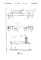
Referring to FIG. 1, aQFP device 10 may be soldered by itsleads 12 to aQFP adapter 14. TheQFP adapter 14 comprises a QFP adapter printedcircuit board 18,pads 16 which are placed to correspond to the device leads, andpins 20. The QFP adapter printedcircuit board 18 may be manufactured by printed circuit board fabrication techniques. Thepins 20 are press fit into plated-through holes therein and thus connected to thepads 16 by conductive elements (e.g., traces) in the insulative body of the QFP adapter circuit board. Thepins 20 may also be soldered to the QFP adapter printedcircuit board 18.
Thepins 20 of theQFP adapter 14 are spaced to engageterminals 24 inchimney connector 22.Chimney connector 22 is fabricated of insulative material such as glass epoxy or molding compounds, and theterminals 24 are low insertion force socket terminals. Theterminals 24 includesolder tails 25 which are soldered to electrical attachment sites onadapter substrate 28.Adapter substrate 28 may also be manufactured by printed circuit board fabrication techniques. Also soldered to theadapter substrate 28 are gullwing-shaped adapter leads 26. These gullwing-shaped adapter leads are electrically connected to the electrical attachment sites by conductive elements supported by the insulative body of theadapter substrate 28.
As shown in FIG. 5, the gullwing-shaped adapter leads 26 are manufactured from asingle lead frame 50 which is soldered to the top surface ofadapter substrate 28. Thecorners 52 oflead frame 50 are then removed (FIG. 6). A jig (not shown) is then pressed onto the top ofleads 26 to hold them firmly toadapter substrate 28, and the leads are bent in two different directions to form the opposing curves of a gullwing shape (FIGS. 7 and 8). The jig prevents the solder joints from being subjected to excessive stress during the bending operation. The remainder of theedges 54 of thelead frame 50 are then cut (FIG. 9) to form the final gullwing-shaped adapter leads 26 (FIG. 10).
Leads 26 thus include feet adapted to be soldered to standard QFP spacedpads 31 oncircuit board surface 30 by the end user with surface mount soldering techniques, as shown in FIG. 2.Strain relief elements 32 may optionally be mounted on the adapter substrate and soldered to thecircuit board 31. The strain relief elements may be soldered in holes in the circuit surface as shown in FIG. 2, or shorter strain relief elements may be soldered to pads on the circuit surface.
Once theleads 26 on the adapter substrate are soldered to thecircuit board surface 30, the user may insert theQFP adapter 14 with adevice 10 soldered to it. To change devices (e.g., for the purpose of experimentation, upgrading or repair), the QFP adapter board may be removed 5 fromchimney connector 22 and replaced with another adapter board carrying another device.
Referring now to FIG. 3, an adapter is presented which is configured to receive adevice 10 in asocket 38. Quad flat pack sockets as shown are available from sources such as AMP or 3M. In this embodiment, thesocket 38 includespins 40 which may be inserted inreceptacles 36 in thesocket adapter 34.
Thesocket adapter 34 is made up of a socketadapter circuit board 37 which includespins 20 which are connected to thereceptacles 36 by traces in the socket adapter circuit board.Pins 20 are adapted to engage theterminals 24 in thechimney connector 22.
Referring to FIG. 4, once the adapter leads 26 on theadapter substrate 28 are soldered to thecircuit board surface 30, the user may insert thesocket adapter 34 into thechimney connector 22. Adevice 10 may then be inserted into thesocket 38. To change devices, thedevice 10 may be removed fromsocket 38 and replaced with another device.
It should be noted that thesocket adapter 34 can be made to have the same pin configuration as theQFP adapter 14 thus making the parts interchangeable on thesame chimney connector 22.
If this degree of flexibility is not required, thesocket adapter 34 may be directly soldered to theadapter substrate 28 by means ofpins 20. Of course, thereceptacles 36 should be prevented from touching adapter leads 26 (e.g., by using standoffs). This results in a simpler adapter with a lower profile (not shown).
It is also possible to eliminatereceptacles 36 by simply soldering thesocket 38 to thesocket adapter 34. This will also contribute to a simpler and somewhat lower profile adapter (not shown).
Furthermore, thesocket 38 may be a QFP socket, or it may accommodate other device types, such as LCC, PLCC or PGA packages, for example.
Moreover, the parts of the adapter that are implemented with printed circuit boards may be built using embedded lead frames as discussed in my co-pending application, entitled "Molded-in Lead Frames", Ser. Nos. 121,568 and 272,074, which are herein incorporated by reference. For example, in the adapter substrate, thelead frame 50 which is manipulated to form the gullwing-shaped adapter leads may also serve to form conductive elements within the adapter substrate. Such a construction would be less expensive to manufacture than those in which the conductive elements are traces formed using printed circuit board fabrication methods.
The adapter may also be implemented using the molding process discussed in my application entitled "Molded Integrated Circuit Package", Ser. No. 07/564,406, which is herein incorporated by reference.
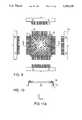
Referring to FIG. 11, the structure of an adapter made using this method includes a plastic moldedchimney connector 60 that accepts aQFP adapter 14 and its associated device. Leads are mounted on the lower surface of the plastic molded chimney connector and connected to theterminals 68 within the chimney.
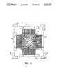
In manufacturing this adapter, a plasticchimney connector body 61 is first molded in a first-shot molding process. As shown in FIG. 12, on the bottom of the body aregrooves 62 that each extend from the edge of the body to the bottom of a hole for holding one of the terminals. At the hole, the channel forms an eye-shapedarea 64 around the bottom aperture of the hole.
Referring to FIG. 13, an associatedlead frame 74 is then placed on the bottom surface of the body so that eachindividual lead 76 rests in its correspondingchannel 62. It will be observed that eye-shapedportions 75 of the leads will rest in their corresponding eye-shapedareas 64. Referring to FIG. 14a, it can be seen that theridges 63 between thegrooves 62 are thicker than theleads 76 themselves.
FIG. 14b shows the first-shot portion of the body after the second operation. The second operation involves the application of heat to the areas between the grooves by pressing on the first-shot portion using a hot metal iron. This application of heat softens the plastic and causes it to surround the leads and thus secure them to the first-shot portion. Since the ridges between the grooves extend beyond the lead frame, there will be a small amount of excess material that will be pressed so as to fill the small voids between the leads and the walls of the grooves.
In performing this operation, the iron is held at a temperature between 425 and 450 degrees fahrenheit, and applied to the chimney connector body with a force of 30 p.s.i.g.
With the leads secured in place, theterminals 68 may be installed in the chimney and connected to theeyes 75 of the leads 76. The electrical connection may be made by soldering or press-fitting, for example. The lead frame may then be cut and bent to leave the gullwing-shaped leads. This may require applying a force to hold the leads in place during the bending operation.
If desired, further material can be added to the chimney in a second-shot molding operation. This further material assists in holding the leads in place. It is also possible to glue the lead frames in place instead of heat sealing them.
Referring to FIG. 15, another embodiment of aQFP adapter 110 includes a circuit bearing element, such as a printedcircuit board element 112, with plated, or otherwise metalized, holes 113 that accept bent gullwing-shaped leads 114. These leads are soldered to the circuit board element at one end and include feet at the other end which may be soldered to pads arranged in four rows on amother circuit board 116 or mounted in a suitable socket (not shown). Other interconnect elements, such asreceptacles 118 embedded inchimney 119 are also connected to thecircuit board element 112 and allow for connection to external circuitry.
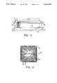
Referring to FIGS. 16 and 17, alead frame 120 for use in assembling an adapter according to the invention includes aframe portion 122 andlead elements 124. The lead frame may be made by stamping or etching or by any other suitable method.
In assembling an adapter, thelead elements 124 of the lead frame are first bent (FIG. 18) to a hook-shape in a bending apparatus. Once bent, the lead frame ends are inserted in corresponding holes in the printedcircuit board 112, and the lead elements are anchored in place, for example, by infra-red soldering (FIG. 19). With the lead frame soldered in place, its corners 123 (FIG. 16) are cut away. The leads are then bent to their final gullwing shape (FIG. 20) in a second bending operation and the remaining side frame portions 121 (FIG. 16) are cut away.
It is observed that it is important to be careful to prevent solder from flowing substantially away from the solder holes along the lead frame during soldering, as this solder may interfere with the second bending operation.
The second bending operation and the cutting operation may be performed in a single operation using a bending apparatus. Referring to FIG. 21, the soldered butunfinished adapter 110 is placed on apedestal 130, and thebending tool 140 is lowered onto the part. Upon lowering the tool, a spring-loadedjaw 132 first engages the adapter and holds it in place on its pedestal. As the tool continues to descend, four bending implements 136 engage the leads and bend them around bending dies 142 on the pedestal. These dies are designed to guide the leads down around the edges of the top of the printed circuit element and impart them with the opposing curves and feet of a gullwing shape. They are also dimensioned to allow for a certain amount of overbending, so that the leads spring into their specified shape when the implements are retracted. Finally, as the tool reaches the end of its stroke, four blades 136 cut away the remaining side portions 121 (FIG. 16) of the frame portion of the lead frame.
The above manufacturing process has the advantage of performing several steps in a single operation with a single tool. It is, of course, possible to separate the cutting and bending operations into separate individual operations.
The unfinished adapter is now ready for further operations, such as the addition of achimney 119 and embedded receptacles as shown in FIG. 15. These receptacles may be electrically connected to attachment sites on the printed circuit element. These sites are connected to the leads by circuit elements, such as copper traces within the printed circuit element, thus providing connections between the receptacles and the leads. Through-hole-type pins may also be provided on the adapter, for the purpose of reinforcing the mechanical connection between the adapter and the mother circuit board, when soldered in place.
Ceramic quad flat pack devices may be used with this invention as well as plastic quad flat pack devices (PQFP).
Other embodiments are within the scope of the following claims.
Claims (32)
1. An adapter for removably electrically connecting the device leads of an electronic device to a circuit surface on which there are contacts arranged in a pattern having four rows of contacts, one row on each side of a rectangular pattern, the device leads of the electronic device being disposed in essentially the same rectangular pattern as that of the contacts on the circuit surface, said adapter comprising:
an insulative body bearing electrical attachment sites configured for making electrical connections with said device leads of the electronic device;
a plurality of adapter leads formed from lead frame portions, each said adapter lead extending outwardly from said body and bending downwardly below said body and then further outwardly in a pair of opposing curves to form a foot, said adapter leads together forming feet located in a pattern that matches both said contacts on said circuit surface and the device leads of the electronic device; and
a plurality of terminal elements supported by said body and electrically connecting said adapter leads to said electrical attachment sites,
said terminal elements being disposed such that each said terminal element lies substantially directly under the electronic device.
2. An adapter for removably electrically connecting the device leads of an electronic device of the type having four rows of gullwing-shaped leads disposed on the sides of a rectangular pattern to a circuit surface on which there are contacts arranged in a pattern having four rows of contacts, one row on each side of a rectangular pattern, said adapter comprising:
a first insulative body;
electrical attachment sites on said body for making electrical connections with said electronic device;
a plurality of lead frame portions, each including
an adapter lead extending outwardly from said body and bending downwardly below said body and then further outwardly in a pair of opposing curves, each said adapter lead having ends forming feet located in a pattern matching that of said contacts on said circuit surface; and
a conductive element supported by said body and connecting said adapter lead to one of said electrical attachment sites;
a first electrical connector connected at said electrical attachment sites for making connections to said device leads; and
a second insulative body with a second series of electrical attachment sites configured for making connections to said gullwing-shaped leads,
a second connector, separate from said second body, configured to mate with said first connector, said connector comprising a plurality of electrical connector elements and
conductive elements supported on said second body for making electrical connections between said second connector and said second series of electrical attachment sites.
3. An adapter for removably electrically connecting the device leads of an electronic device of the type having four rows of gullwing-shaped leads disposed on the sides of a rectangular pattern to a circuit surface on which there are contacts arranged in a pattern having four rows of contacts, one row on each side of a rectangular pattern, said adapter comprising:
a first insulative body;
electrical attachment sites on said body for making electrical connections with said electronic device;
a plurality of lead frame portions, each including
an adapter lead extending outwardly from said body and bending downwardly below said body and then further outwardly in a pair of opposing curves, each said adapter lead having ends forming feet located in a pattern matching that of said contacts on said circuit surface; and
a conductive element supported by said body and connecting said adapter lead to one of said electrical attachment sites;
a first electrical connector connected at said electrical attachment sites for making connections to said device leads; and
a second insulative body with a second series of electrical attachment sites configured for making connections to said gullwing-shaped leads,
a second connector configured to mate with said first connector,
conductive elements supported on said second body for making electrical connections between said second connector and said second series of electrical attachment sites, and
at least one strain relief element affixed to said adapter for mechanical connection to the circuit surface.
4. An adapter for removably electrically connecting the device leads of an electronic device of the type having four rows of gullwing-shaped leads disposed on the sides of a rectangular pattern to a circuit surface on which there are contacts arranged in a pattern having four rows of contacts, one row on each side of a rectangular pattern, said adapter comprising:
a first insulative body;
electrical attachment sites on said body for making electrical connections with said electronic device;
a plurality of lead frame portions, each including
an adapter lead extending outwardly from said body and bending downwardly below said body and then further outwardly in a pair of opposing curves, each said adapter lead having ends forming feet located in a pattern matching that of said contacts on said circuit surface; and
a conductive element supported by said body and connecting said adapter lead to one of said electrical attachment sites;
a first electrical connector connected at said electrical attachment sites for making connections to said device leads; and
a second insulative body with a second series of electrical attachment sites configured for making connections to said gullwing-shaped leads,
a second connector configured to mate with said first connector, said connector comprising a plurality of socket terminals and
conductive elements supported on said second body for making electrical connections between said second connector and said second series of electrical attachment sites.
5. An adapter for removably electrically connecting the leads of an electronic device to a circuit surface, wherein said leads are gullwing-shaped leads disposed in four rows, one on each of four sides of a rectangular pattern, and wherein said circuit surface has contacts disposed in essentially the same rectangular pattern as that of the electronic device, said adapter comprising
an insulative adapter body;
contacts on said adapter body, said contacts being configured for making electrical connections to the leads of the device and being disposed in a pattern matching that of said device leads;
adapter leads extending from said adapter body for making electrical connections to the circuit surface, each said adapter lead extending outwardly from said adapter body and bending downwardly below said body and then further outwardly in a pair of opposing curves, said adapter leads having ends, and said ends of said adapter leads forming feet located in a pattern matching that of said contacts on said circuit surface; and
a plurality of terminal elements supported by said adapter body and electrically connecting said adapter leads to said contacts on said adapter body,
said terminal elements being disposed such that each said terminal element lies substantially directly under the electronic device.
6. The adapter of claim 5 wherein said adapter leads are gullwing-shaped.
7. The adapter of claim 5 wherein said electronic device is a quad flat pack device.
8. The subject matter of claim 5 wherein said contacts on the circuit surface are conductive pads.
9. The adapter of claim 5 wherein said adapter body comprises a plurality of body portions electrically connected in a vertical stack.
10. The adapter f claim 9 wherein said adapter body comprises an upper portion on which said contacts are supported and a lower portion from which said adapter leads extend, and wherein said terminal elements comprise electrical connectors providing separable electrical connections between said upper and lower portions.
11. The adapter of claim 5, wherein said adapter body comprises
a first insulative body portion;
electrical attachment sites on said body portion for making electrical connections with said electronic device; and
conductive elements supported by said body portion and connecting said adapter leads to said electrical attachment sites.
12. The adapter of claim 11 wherein said conductive elements and said adapter leads are portions of a lead frame, and said body portion comprises portions molded around said lead frame.
13. The adapter of claim 11 wherein said conductive elements and said adapter leads are portions of a lead frame, and said lead frame is sealed in said body portion.
14. The adapter of claim 11 wherein said body portion is a substrate on which said conductive elements are supported.
15. The adapter of claim 14 wherein said conductive elements are printed circuit paths and said substrate is a printed circuit board.
16. The adapter of claim 11, wherein said adapter body further comprises a first electrical connector connected at said electrical attachment sites for making connections to said leads of the electronic device.
17. The adapter of claim 16 wherein said first electrical connector comprises a body portion separate from said first body portion.
18. The adapter of claim 16 wherein said first electrical connector comprises said terminal elements, and said terminal elements comprise a plurality of socket terminals.
19. The adapter of claim 16 wherein said adapter body further comprises
a second insulative body portion with a second series of electrical attachment sites configured for making connections to said gullwing-shaped leads of said device,
a second connector configured to mate with said first connector, and
second conductive elements supported on said second body portion for making electrical connections between said second connector and said second series of electrical attachment sites.
20. The adapter of claim 19 wherein said second connector comprises a plurality of electrical connector elements supported in said second connector.
21. The adapter of claim 19 wherein said attachment sites on said second body portion are contact pads configured for making solder connections to said gullwing-shaped leads of the device.
22. The adapter of claim 19 wherein said second body portion comprises a printed circuit board and said conductive elements are printed circuit paths on said board.
23. The adapter of claim 19 wherein said conductive elements of said second body portion comprise portions of a lead frame, and said second body portion comprises portions molded around said lead frame.
24. An adapter for removably electrically connecting the leads of an electronic device to a circuit surface, wherein said leads are gullwing-shaped and disposed in four rows, one on each of four sides of a rectangular pattern, and wherein said circuit surface has contacts disposed in essentially the same rectangular pattern as that of the electronic device, said adapter comprising
an insulative adapter body;
contacts on said adapter body, said contacts being configured for making electrical connections to the leads of the device and being disposed in a pattern matching that of said device leads; and
adapter leads extending from said adapter body for making electrical connections to the circuit surface, each said adapter lead extending outwardly from said adapter body and bending downwardly below said body and then further outwardly in a pair of opposing curves, said adapter leads having ends, and said ends of said adapter leads forming feet located in a pattern matching that of said contacts on said circuit surface,
said adapter body comprising
a first insulative body portion;
electrical attachment sites on said body portion for making electrical connections with said electronic device;
conductive elements supported by said body portion and connecting said adapter leads to said electrical attachment sites;
a first electrical connector connected at said electrical attachment sites for making connections to said device leads;
a second insulative body portion with a second series of electrical attachment sites configured for making connections to said gullwing-shaped leads of said device;
a second connector configured to mate with said first connector; and
second conductive elements supported on said second body portion for making electrical connections between said second connector and said second series of electrical attachment sites,
wherein the electronic device is of the type having four rows of gullwing-shaped leads disposed on the sides of a rectangular pattern, and wherein said second connector comprises a body portion separate from said second body portion.
25. An adapter for removably electrically connecting the leads of an electronic device to a circuit surface, wherein said leads are gullwing-shaped and disposed in four rows, one on each of four sides of a rectangular pattern, and wherein said circuit surface has contacts disposed in essentially the same rectangular pattern as that of the electronic device, said adapter comprising
an insulative adapter body;
contacts on said adapter body, said contacts being configured for making electrical connections to the leads of the device and being disposed in a pattern matching that of said device leads;
adapter leads extending form said adapter body for making electrical connections to the circuit surface, each said adapter lead extending outwardly from said adapter body and bending downwardly below said body and then further outwardly in a pair of opposing curves, said adapter leads having ends, and said ends of said adapter leads forming feet located in a pattern matching that of said contacts on said circuit surface; and
at least one strain relief element affixed to said adapter for mechanical connection to the circuit surface,
said adapter body comprising
a first insulative body portion;
electrical attachment sites on said body portion for making electrical connections with said electronic device;
conductive elements supported by said body portion and connecting said adapter leads to said electrical attachment sites;
a first electrical connector connected at said electrical attachment sites for making connections to said device leads;
a second insulative body portion with a second series of electrical attachment sites configured for making connections to said gullwing-shaped leads of said device;
a second connector configured to mate with said first connector; and
second conductive elements supported on said second body portion for making electrical connections between said second connector and said second series of electrical attachment sites,
wherein the electronic device is of the type having four rows of gullwing-shaped leads disposed on the sides of a rectangular pattern.
26. An adapter for removably electrically connecting the leads of an electronic device to a circuit surface, wherein said leads are gullwing-shaped and disposed in four rows, one on each of four sides of a rectangular pattern, and wherein said circuit surface has contacts disposed in essentially the sam rectangular pattern as that of the electronic device, said adapter comprising
an insulative adapter body;
contacts on said adapter body, said contacts being configured for making electrical connections to the leads of the device and being disposed in a pattern matching that of said device leads; and
adapter leads extending from said adapter body for making electrical connections to the circuit surface, each said adapter lead extending outwardly form said adapter body and bending downwardly below said body and then further outwardly in a pair of opposing curves, said adapter leads having ends, and said ends of said adapter leads forming feet located in a pattern matching that of said contacts on said circuit surface,
said adapter body comprising
a first insulative body portion;
electrical attachment sites on said body portion for making electrical connections with said electronic device;
conductive elements supported by said body portion and connecting said adapter leads to said electrical attachment sites;
a first electrical connector connected at said electrical attachment sites for making connections to said device leads;
a second insulative body portion with a second series of electrical attachment sites configured for making connections to said gullwing-shaped leads of said device;
a second connector configured to mate with said first connector; and
second conductive elements supported on said second body portion for making electrical connections between said second connector and said second series of electrical attachment sites,
wherein the electronic device is of the type having four rows of gullwing-shaped leads disposed on the sides of a rectangular pattern, and wherein said second connector comprises a plurality of socket terminals.
27. An adapter for removably electrically connecting the gullwing-shaped leads of a quad flat pack electronic device to a circuit surface, wherein said leads are disposed in four rows, one on each of four sides of a rectangular pattern, and wherein said circuit surface has contacts disposed in essentially the same rectangular pattern as that of the electronic device, said adapter comprising
a first insulative body bearing electrical attachment sites,
adapter leads extending from said first insulative body for making electrical connections to the circuit surface, each said adapter lead extending outwardly from said adapter body and bending downwardly below said body and then further outwardly in a pair of opposing, gullwing-shaped curves, said adapter leads having ends, and said ends of said adapter leads forming feet located in a pattern matching that of said contacts on said circuit surface,
first conductive elements supported by said first insulative body and connecting said adapter leads to said electrical attachment sites,
a chimney connector including a plurality of receptacles connected to said attachment sites in said first insulative body,
a second insulative body with a second plurality of electrical attachment sites configured for making connection to said gullwing-shaped leads of said quad flat pack device,
a plurality of posts supported by said second body and configured to mate with said receptacles,
second conductive elements supported on said second body for making electrical connections between said posts and said second plurality of electrical attachment sites, and
at least one strain relief element affixed to said adapter for mechanical connection to the circuit surface.
28. An adapter for removably electrically connecting the gullwing-shaped leads of a quad flat pack electronic device to a circuit surface, wherein said leads are disposed in four rows, one on each of four sides of a rectangular pattern, and wherein said circuit surface has contacts disposed in essentially the same rectangular pattern as that of the electronic device, said adapter comprising
a first insulative body bearing electrical attachment sites,
adapter leads extending from said first insulative body for making electrical connections to the circuit surface, each said adapter lead extending outwardly from said adapter body and bending downwardly below said body and then further outwardly in a pair of opposing, gullwing-shaped curves, said adapter leads having ends, and said ends of said adapter leads forming feet located in a pattern matching that of said contacts on said circuit surface,
first conductive elements supported by said first insulative body and connecting said adapter leads to said electrical attachment sites,
a chimney connector including a first plurality of receptacles connected to said attachment sites in said first insulative body,
a second insulative body bearing a second plurality of receptacles, a first plurality of posts configured to mate with said first plurality of receptacles, and second conductive elements supported on said second body for making electrical connections between said first plurality of posts and said second plurality of receptacles, and
a third insulative body bearing a second plurality of posts for connection to said second plurality of receptacles, and a plurality of electrical connection sites configured for making connections to said gullwing-shaped leads of said quad flat pack device, said connection sites and said posts being electrically connected.
29. The adapter of claim 28 wherein said first conductive elements in said first body are printed circuit paths and said first insulative body is a printed circuit board.
30. The adapter of claim 28 wherein said first conductive elements in said first body and said adapter leads are portions of a lead frame, and said body comprises portions molded around said lead frame.
31. The adapter of claim 28 further including at least one strain relief element affixed to said adapter for mechanical connection to the circuit surface.
32. The adapter of claim 28 wherein said connection sites on said third body are contact pads configured for making solder connections to said gullwing-shaped leads of the device.
Priority Applications (1)
| Application Number | Priority Date | Filing Date | Title |
|---|---|---|---|
| US07/693,446US5151039A (en) | 1990-04-06 | 1991-04-29 | Integrated circuit adapter having gullwing-shaped leads |
Applications Claiming Priority (2)
| Application Number | Priority Date | Filing Date | Title |
|---|---|---|---|
| US50573390A | 1990-04-06 | 1990-04-06 | |
| US07/693,446US5151039A (en) | 1990-04-06 | 1991-04-29 | Integrated circuit adapter having gullwing-shaped leads |
Related Parent Applications (1)
| Application Number | Title | Priority Date | Filing Date |
|---|---|---|---|
| US50573390AContinuation-In-Part | 1990-04-06 | 1990-04-06 |
Publications (1)
| Publication Number | Publication Date |
|---|---|
| US5151039Atrue US5151039A (en) | 1992-09-29 |
Family
ID=27055234
Family Applications (1)
| Application Number | Title | Priority Date | Filing Date |
|---|---|---|---|
| US07/693,446Expired - Fee RelatedUS5151039A (en) | 1990-04-06 | 1991-04-29 | Integrated circuit adapter having gullwing-shaped leads |
Country Status (1)
| Country | Link |
|---|---|
| US (1) | US5151039A (en) |
Cited By (116)
| Publication number | Priority date | Publication date | Assignee | Title |
|---|---|---|---|---|
| US5318451A (en)* | 1993-01-25 | 1994-06-07 | Augat Inc. | Stackable interconnection socket |
| DE4408356A1 (en)* | 1994-03-14 | 1995-09-21 | Ralf Dipl Ing Bierschenk | Circuit adaptor device |
| US5562462A (en)* | 1994-07-19 | 1996-10-08 | Matsuba; Stanley | Reduced crosstalk and shielded adapter for mounting an integrated chip package on a circuit board like member |
| US5619108A (en)* | 1994-07-13 | 1997-04-08 | Mitsubishi Denki Kabushiki Kaisha | Vehicle alternating-current generator control device and vehicle alternating-current generator |
| US5667388A (en)* | 1994-11-14 | 1997-09-16 | Intel Corporation | Printed circuit board adapter carrier for input/output cards |
| DE29620593U1 (en)* | 1996-11-26 | 1998-01-02 | Siemens AG, 80333 München | Socket for an integrated circuit |
| US6126457A (en)* | 1997-10-17 | 2000-10-03 | General Motors Corporation | Routed wire electrical center adapter |
| WO2000008675A3 (en)* | 1998-08-05 | 2000-10-12 | David D Kan | Adapter for surface mounted devices |
| US6407652B1 (en) | 1998-11-19 | 2002-06-18 | Pulse Research Lab | Adapters for RF connectors |
| US6494739B1 (en) | 2001-02-07 | 2002-12-17 | Welch Allyn, Inc. | Miniature connector with improved strain relief for an imager assembly |
| US20040056338A1 (en)* | 1999-12-16 | 2004-03-25 | Crowley Sean Timothy | Near chip size semiconductor package |
| US20040061217A1 (en)* | 1999-10-15 | 2004-04-01 | Ku Jae Hun | Thin and heat radiant semiconductor package and method for manufacturing |
| US20040087216A1 (en)* | 2002-10-29 | 2004-05-06 | Hofmeister Rudolf J. | Electrical adapter for protecting electrical interfaces |
| US20040097016A1 (en)* | 1998-11-20 | 2004-05-20 | Yee Jae Hak | Semiconductor package and method of making leadframe having lead locks to secure leads to encapsulant |
| US20040227217A1 (en)* | 1999-10-15 | 2004-11-18 | Jang Sung Sik | Semiconductor package having improved adhesiveness and ground bonding |
| US6844615B1 (en) | 2003-03-13 | 2005-01-18 | Amkor Technology, Inc. | Leadframe package for semiconductor devices |
| US6846704B2 (en) | 2001-03-27 | 2005-01-25 | Amkor Technology, Inc. | Semiconductor package and method for manufacturing the same |
| US20050029636A1 (en)* | 2000-12-29 | 2005-02-10 | Paek Jong Sik | Semiconductor package including flip chip |
| US20050062148A1 (en)* | 2000-03-25 | 2005-03-24 | Seo Seong Min | Semiconductor package |
| US20050062139A1 (en)* | 2003-09-24 | 2005-03-24 | Chung-Hsing Tzu | Reinforced die pad support structure |
| US6873041B1 (en) | 2001-11-07 | 2005-03-29 | Amkor Technology, Inc. | Power semiconductor package with strap |
| US6873032B1 (en) | 2001-04-04 | 2005-03-29 | Amkor Technology, Inc. | Thermally enhanced chip scale lead on chip semiconductor package and method of making same |
| US6893900B1 (en) | 1998-06-24 | 2005-05-17 | Amkor Technology, Inc. | Method of making an integrated circuit package |
| US20050139969A1 (en)* | 2002-09-09 | 2005-06-30 | Lee Choon H. | Semiconductor package with increased number of input and output pins |
| US20050156292A1 (en)* | 2001-01-15 | 2005-07-21 | Paek Jong S. | Reduced size semiconductor package with stacked dies |
| US6965157B1 (en) | 1999-11-09 | 2005-11-15 | Amkor Technology, Inc. | Semiconductor package with exposed die pad and body-locking leadframe |
| US6967395B1 (en) | 2001-03-20 | 2005-11-22 | Amkor Technology, Inc. | Mounting for a package containing a chip |
| US6998702B1 (en) | 2001-09-19 | 2006-02-14 | Amkor Technology, Inc. | Front edge chamfer feature for fully-molded memory cards |
| US7001799B1 (en) | 2003-03-13 | 2006-02-21 | Amkor Technology, Inc. | Method of making a leadframe for semiconductor devices |
| US7005326B1 (en) | 1998-06-24 | 2006-02-28 | Amkor Technology, Inc. | Method of making an integrated circuit package |
| US20060051989A1 (en)* | 2004-09-08 | 2006-03-09 | Advanced Interconnections Corporation | Multiple piece shroud |
| US7030474B1 (en) | 1998-06-24 | 2006-04-18 | Amkor Technology, Inc. | Plastic integrated circuit package and method and leadframe for making the package |
| US7045883B1 (en) | 2001-04-04 | 2006-05-16 | Amkor Technology, Inc. | Thermally enhanced chip scale lead on chip semiconductor package and method of making same |
| US7057268B1 (en) | 2004-01-27 | 2006-06-06 | Amkor Technology, Inc. | Cavity case with clip/plug for use on multi-media card |
| US7064009B1 (en) | 2001-04-04 | 2006-06-20 | Amkor Technology, Inc. | Thermally enhanced chip scale lead on chip semiconductor package and method of making same |
| US7071541B1 (en) | 1998-06-24 | 2006-07-04 | Amkor Technology, Inc. | Plastic integrated circuit package and method and leadframe for making the package |
| US20060151858A1 (en)* | 2000-04-27 | 2006-07-13 | Ahn Byung H | Leadframe and semiconductor package made using the leadframe |
| US7091594B1 (en) | 2004-01-28 | 2006-08-15 | Amkor Technology, Inc. | Leadframe type semiconductor package having reduced inductance and its manufacturing method |
| US7112474B1 (en) | 1998-06-24 | 2006-09-26 | Amkor Technology, Inc. | Method of making an integrated circuit package |
| US7115445B2 (en) | 1999-10-15 | 2006-10-03 | Amkor Technology, Inc. | Semiconductor package having reduced thickness |
| US7138707B1 (en) | 2003-10-21 | 2006-11-21 | Amkor Technology, Inc. | Semiconductor package including leads and conductive posts for providing increased functionality |
| US7144517B1 (en) | 2003-11-07 | 2006-12-05 | Amkor Technology, Inc. | Manufacturing method for leadframe and for semiconductor package using the leadframe |
| US20060289973A1 (en)* | 2001-03-27 | 2006-12-28 | Lee Hyung J | Lead frame for semiconductor package |
| US20070026719A1 (en)* | 2005-08-01 | 2007-02-01 | Hon Hai Precision Ind. Co., Ltd. | Low insertion force socket with lead-in mechanism background of the invention |
| US7190062B1 (en) | 2004-06-15 | 2007-03-13 | Amkor Technology, Inc. | Embedded leadframe semiconductor package |
| US7192807B1 (en) | 2002-11-08 | 2007-03-20 | Amkor Technology, Inc. | Wafer level package and fabrication method |
| US7202554B1 (en) | 2004-08-19 | 2007-04-10 | Amkor Technology, Inc. | Semiconductor package and its manufacturing method |
| US7211879B1 (en) | 2003-11-12 | 2007-05-01 | Amkor Technology, Inc. | Semiconductor package with chamfered corners and method of manufacturing the same |
| US7217991B1 (en) | 2004-10-22 | 2007-05-15 | Amkor Technology, Inc. | Fan-in leadframe semiconductor package |
| US7245007B1 (en) | 2003-09-18 | 2007-07-17 | Amkor Technology, Inc. | Exposed lead interposer leadframe package |
| US20070170560A1 (en)* | 2006-01-26 | 2007-07-26 | Gaucher Brian P | Apparatus and methods for packaging integrated circuit chips with antennas formed from package lead wires |
| US20070176287A1 (en)* | 1999-11-05 | 2007-08-02 | Crowley Sean T | Thin integrated circuit device packages for improved radio frequency performance |
| US7253503B1 (en) | 1999-11-05 | 2007-08-07 | Amkor Technology, Inc. | Integrated circuit device packages and substrates for making the packages |
| US20080003722A1 (en)* | 2004-04-15 | 2008-01-03 | Chun David D | Transfer mold solution for molded multi-media card |
| US7332375B1 (en) | 1998-06-24 | 2008-02-19 | Amkor Technology, Inc. | Method of making an integrated circuit package |
| US7361533B1 (en) | 2002-11-08 | 2008-04-22 | Amkor Technology, Inc. | Stacked embedded leadframe |
| US20080157311A1 (en)* | 2006-12-27 | 2008-07-03 | Smith Lee J | Semiconductor Package Having Leadframe with Exposed Anchor Pads |
| US20090014851A1 (en)* | 2007-07-10 | 2009-01-15 | Choi Yeonho | Fusion quad flat semiconductor package |
| US7485952B1 (en) | 2001-09-19 | 2009-02-03 | Amkor Technology, Inc. | Drop resistant bumpers for fully molded memory cards |
| US7507603B1 (en) | 2005-12-02 | 2009-03-24 | Amkor Technology, Inc. | Etch singulated semiconductor package |
| US7572681B1 (en) | 2005-12-08 | 2009-08-11 | Amkor Technology, Inc. | Embedded electronic component package |
| US7598598B1 (en) | 2003-02-05 | 2009-10-06 | Amkor Technology, Inc. | Offset etched corner leads for semiconductor package |
| US20090284940A1 (en)* | 2006-01-19 | 2009-11-19 | Fujitsu Limited | Alignment plate |
| US20090284939A1 (en)* | 2006-01-19 | 2009-11-19 | Fujitsu Limited | Alignment plate |
| US7687899B1 (en) | 2007-08-07 | 2010-03-30 | Amkor Technology, Inc. | Dual laminate package structure with embedded elements |
| US7723852B1 (en) | 2008-01-21 | 2010-05-25 | Amkor Technology, Inc. | Stacked semiconductor package and method of making same |
| US7723210B2 (en) | 2002-11-08 | 2010-05-25 | Amkor Technology, Inc. | Direct-write wafer level chip scale package |
| US7768135B1 (en) | 2008-04-17 | 2010-08-03 | Amkor Technology, Inc. | Semiconductor package with fast power-up cycle and method of making same |
| US7777351B1 (en) | 2007-10-01 | 2010-08-17 | Amkor Technology, Inc. | Thin stacked interposer package |
| US7808084B1 (en) | 2008-05-06 | 2010-10-05 | Amkor Technology, Inc. | Semiconductor package with half-etched locking features |
| US7829990B1 (en) | 2007-01-18 | 2010-11-09 | Amkor Technology, Inc. | Stackable semiconductor package including laminate interposer |
| US7847392B1 (en) | 2008-09-30 | 2010-12-07 | Amkor Technology, Inc. | Semiconductor device including leadframe with increased I/O |
| US7847386B1 (en) | 2007-11-05 | 2010-12-07 | Amkor Technology, Inc. | Reduced size stacked semiconductor package and method of making the same |
| US7875963B1 (en) | 2008-11-21 | 2011-01-25 | Amkor Technology, Inc. | Semiconductor device including leadframe having power bars and increased I/O |
| US7902660B1 (en) | 2006-05-24 | 2011-03-08 | Amkor Technology, Inc. | Substrate for semiconductor device and manufacturing method thereof |
| US7956453B1 (en) | 2008-01-16 | 2011-06-07 | Amkor Technology, Inc. | Semiconductor package with patterning layer and method of making same |
| US7960818B1 (en) | 2009-03-04 | 2011-06-14 | Amkor Technology, Inc. | Conformal shield on punch QFN semiconductor package |
| US7968998B1 (en) | 2006-06-21 | 2011-06-28 | Amkor Technology, Inc. | Side leaded, bottom exposed pad and bottom exposed lead fusion quad flat semiconductor package |
| US7982298B1 (en) | 2008-12-03 | 2011-07-19 | Amkor Technology, Inc. | Package in package semiconductor device |
| US7982297B1 (en) | 2007-03-06 | 2011-07-19 | Amkor Technology, Inc. | Stackable semiconductor package having partially exposed semiconductor die and method of fabricating the same |
| US7989933B1 (en) | 2008-10-06 | 2011-08-02 | Amkor Technology, Inc. | Increased I/O leadframe and semiconductor device including same |
| US8008758B1 (en) | 2008-10-27 | 2011-08-30 | Amkor Technology, Inc. | Semiconductor device with increased I/O leadframe |
| US8026589B1 (en) | 2009-02-23 | 2011-09-27 | Amkor Technology, Inc. | Reduced profile stackable semiconductor package |
| US8058715B1 (en) | 2009-01-09 | 2011-11-15 | Amkor Technology, Inc. | Package in package device for RF transceiver module |
| US8067821B1 (en) | 2008-04-10 | 2011-11-29 | Amkor Technology, Inc. | Flat semiconductor package with half package molding |
| US8072050B1 (en) | 2008-11-18 | 2011-12-06 | Amkor Technology, Inc. | Semiconductor device with increased I/O leadframe including passive device |
| US8089145B1 (en) | 2008-11-17 | 2012-01-03 | Amkor Technology, Inc. | Semiconductor device including increased capacity leadframe |
| US8089159B1 (en) | 2007-10-03 | 2012-01-03 | Amkor Technology, Inc. | Semiconductor package with increased I/O density and method of making the same |
| US8125064B1 (en) | 2008-07-28 | 2012-02-28 | Amkor Technology, Inc. | Increased I/O semiconductor package and method of making same |
| US20120075816A1 (en)* | 2010-09-24 | 2012-03-29 | On Semiconductor Trading, Ltd. | Circuit device and method of manufacturing the same |
| US8184453B1 (en) | 2008-07-31 | 2012-05-22 | Amkor Technology, Inc. | Increased capacity semiconductor package |
| US8294276B1 (en) | 2010-05-27 | 2012-10-23 | Amkor Technology, Inc. | Semiconductor device and fabricating method thereof |
| US8318287B1 (en) | 1998-06-24 | 2012-11-27 | Amkor Technology, Inc. | Integrated circuit package and method of making the same |
| US8324511B1 (en) | 2010-04-06 | 2012-12-04 | Amkor Technology, Inc. | Through via nub reveal method and structure |
| US8390130B1 (en) | 2011-01-06 | 2013-03-05 | Amkor Technology, Inc. | Through via recessed reveal structure and method |
| US8440554B1 (en) | 2010-08-02 | 2013-05-14 | Amkor Technology, Inc. | Through via connected backside embedded circuit features structure and method |
| US8487445B1 (en) | 2010-10-05 | 2013-07-16 | Amkor Technology, Inc. | Semiconductor device having through electrodes protruding from dielectric layer |
| US8487420B1 (en) | 2008-12-08 | 2013-07-16 | Amkor Technology, Inc. | Package in package semiconductor device with film over wire |
| US8552548B1 (en) | 2011-11-29 | 2013-10-08 | Amkor Technology, Inc. | Conductive pad on protruding through electrode semiconductor device |
| US8575742B1 (en) | 2009-04-06 | 2013-11-05 | Amkor Technology, Inc. | Semiconductor device with increased I/O leadframe including power bars |
| US8648450B1 (en) | 2011-01-27 | 2014-02-11 | Amkor Technology, Inc. | Semiconductor device including leadframe with a combination of leads and lands |
| US8674485B1 (en) | 2010-12-08 | 2014-03-18 | Amkor Technology, Inc. | Semiconductor device including leadframe with downsets |
| US8680656B1 (en) | 2009-01-05 | 2014-03-25 | Amkor Technology, Inc. | Leadframe structure for concentrated photovoltaic receiver package |
| US8791501B1 (en) | 2010-12-03 | 2014-07-29 | Amkor Technology, Inc. | Integrated passive device structure and method |
| US8796561B1 (en) | 2009-10-05 | 2014-08-05 | Amkor Technology, Inc. | Fan out build up substrate stackable package and method |
| US8937381B1 (en) | 2009-12-03 | 2015-01-20 | Amkor Technology, Inc. | Thin stackable package and method |
| US9048298B1 (en) | 2012-03-29 | 2015-06-02 | Amkor Technology, Inc. | Backside warpage control structure and fabrication method |
| US9129943B1 (en) | 2012-03-29 | 2015-09-08 | Amkor Technology, Inc. | Embedded component package and fabrication method |
| US9184118B2 (en) | 2013-05-02 | 2015-11-10 | Amkor Technology Inc. | Micro lead frame structure having reinforcing portions and method |
| US9184148B2 (en) | 2013-10-24 | 2015-11-10 | Amkor Technology, Inc. | Semiconductor package and method therefor |
| US9631481B1 (en) | 2011-01-27 | 2017-04-25 | Amkor Technology, Inc. | Semiconductor device including leadframe with a combination of leads and lands and method |
| US9673122B2 (en) | 2014-05-02 | 2017-06-06 | Amkor Technology, Inc. | Micro lead frame structure having reinforcing portions and method |
| US9691734B1 (en) | 2009-12-07 | 2017-06-27 | Amkor Technology, Inc. | Method of forming a plurality of electronic component packages |
| US9704725B1 (en) | 2012-03-06 | 2017-07-11 | Amkor Technology, Inc. | Semiconductor device with leadframe configured to facilitate reduced burr formation |
| US10811341B2 (en) | 2009-01-05 | 2020-10-20 | Amkor Technology Singapore Holding Pte Ltd. | Semiconductor device with through-mold via |
| US20240055786A1 (en)* | 2022-08-12 | 2024-02-15 | Microsoft Technology Licensing, Llc | Assembly fixture for press-fitting contact pins in a printed circuit board assembly |
Citations (8)
| Publication number | Priority date | Publication date | Assignee | Title |
|---|---|---|---|---|
| US4155612A (en)* | 1978-03-03 | 1979-05-22 | Mupac Corporation | Electronic programmable adapter |
| US4354718A (en)* | 1980-08-18 | 1982-10-19 | Amp Incorporated | Dual-in-line package carrier and socket assembly |
| US4560218A (en)* | 1984-12-03 | 1985-12-24 | Amp Incorporated | Socket for surface mount dip |
| US4637670A (en)* | 1984-04-23 | 1987-01-20 | Amp Incorporated | Dual in-line package carrier assembly |
| US4641176A (en)* | 1981-01-26 | 1987-02-03 | Burroughs Corporation | Semiconductor package with contact springs |
| JPS63182577A (en)* | 1987-01-23 | 1988-07-27 | Mitsubishi Electric Corp | IC tester |
| US4766478A (en)* | 1986-09-02 | 1988-08-23 | Dennis Richard K | Lead frame for semi-conductor device and process of connecting same |
| US4907976A (en)* | 1988-03-01 | 1990-03-13 | Killy Corporation | Connector |
- 1991
- 1991-04-29USUS07/693,446patent/US5151039A/ennot_activeExpired - Fee Related
Patent Citations (8)
| Publication number | Priority date | Publication date | Assignee | Title |
|---|---|---|---|---|
| US4155612A (en)* | 1978-03-03 | 1979-05-22 | Mupac Corporation | Electronic programmable adapter |
| US4354718A (en)* | 1980-08-18 | 1982-10-19 | Amp Incorporated | Dual-in-line package carrier and socket assembly |
| US4641176A (en)* | 1981-01-26 | 1987-02-03 | Burroughs Corporation | Semiconductor package with contact springs |
| US4637670A (en)* | 1984-04-23 | 1987-01-20 | Amp Incorporated | Dual in-line package carrier assembly |
| US4560218A (en)* | 1984-12-03 | 1985-12-24 | Amp Incorporated | Socket for surface mount dip |
| US4766478A (en)* | 1986-09-02 | 1988-08-23 | Dennis Richard K | Lead frame for semi-conductor device and process of connecting same |
| JPS63182577A (en)* | 1987-01-23 | 1988-07-27 | Mitsubishi Electric Corp | IC tester |
| US4907976A (en)* | 1988-03-01 | 1990-03-13 | Killy Corporation | Connector |
Non-Patent Citations (17)
| Title |
|---|
| "Advanced Interconnections Catalog #8, Quad. Flat Pack Adaptors" pp. 67-69, 1988. |
| Advanced Interconnections Catalog 8, Quad. Flat Pack Adaptors pp. 67 69, 1988.* |
| Advanced Interconnections drawing, 2420 A.* |
| Advanced Interconnections drawing, 2420-A. |
| Advanced Interconnections, drawings SK 2265, SK 2376, 3049 2A, 3049 2B, 3049 2, FAB3049 2B, 3049, 3093,3049, 3078REF, 3078 A, FAB3078(1 and 2), 3078, 3079, and Motorola, drawing entitled 132 PIN PQFP Adapter PWB .* |
| Advanced Interconnections, drawings SK 2309 Rev O, SK 2309 Rev 1, and SK 2309 Sheet 20F2.* |
| Advanced Interconnections, drawings SK-2265, SK-2376, 3049-2A, 3049-2B, 3049-2, FAB3049-2B, 3049, 3093,3049, 3078REF, 3078-A, FAB3078(1 and 2), 3078, 3079, and Motorola, drawing entitled "132 PIN PQFP Adapter PWB". |
| Advanced Interconnections, drawings SK-2309 Rev O, SK-2309 Rev 1, and SK-2309 Sheet 20F2. |
| Advanced Interconnections, Letter from Jack Reilly and drawings SK 2265, SK 2264, SK 2263, SK 2262.* |
| Advanced Interconnections, Letter from Jack Reilly and drawings SK-2265, SK-2264, SK-2263, SK-2262. |
| Die Tech, drawings CZ 5700 PKG. Cross Section, CZ 5700 PKG. 150, CZ 5701 PKG. Assy. DP., and Die Tech s Advanced Technologies One Source for Solutions , promotional item.* |
| Die-Tech, drawings CZ-5700-PKG. Cross Section, CZ-5700-PKG. 150, CZ-5701-PKG. Assy.-DP., and "Die-Tech's Advanced Technologies-One Source for Solutions", promotional item. |
| Letter by Jay Hartvigsen from Motorola to Advanced Interconnections.* |
| Letter from Analog Devices; Advanced Interconnections catalog #9, pp. 73 and 77. |
| Letter from Analog Devices; Advanced Interconnections catalog 9, pp. 73 and 77.* |
| Quote from Advanced Interconnections to Motorola, Inc.* |
| Raychem, advertisement for SolderQuick Tape (seven pages).* |
Cited By (215)
| Publication number | Priority date | Publication date | Assignee | Title |
|---|---|---|---|---|
| US5318451A (en)* | 1993-01-25 | 1994-06-07 | Augat Inc. | Stackable interconnection socket |
| WO1994017574A1 (en)* | 1993-01-25 | 1994-08-04 | Augat Inc. | Stackable interconnection socket |
| US5429511A (en)* | 1993-01-25 | 1995-07-04 | Augat Inc. | Stackable interconnection socket |
| DE4408356A1 (en)* | 1994-03-14 | 1995-09-21 | Ralf Dipl Ing Bierschenk | Circuit adaptor device |
| US5619108A (en)* | 1994-07-13 | 1997-04-08 | Mitsubishi Denki Kabushiki Kaisha | Vehicle alternating-current generator control device and vehicle alternating-current generator |
| US5562462A (en)* | 1994-07-19 | 1996-10-08 | Matsuba; Stanley | Reduced crosstalk and shielded adapter for mounting an integrated chip package on a circuit board like member |
| US5667388A (en)* | 1994-11-14 | 1997-09-16 | Intel Corporation | Printed circuit board adapter carrier for input/output cards |
| DE29620593U1 (en)* | 1996-11-26 | 1998-01-02 | Siemens AG, 80333 München | Socket for an integrated circuit |
| US6126457A (en)* | 1997-10-17 | 2000-10-03 | General Motors Corporation | Routed wire electrical center adapter |
| US7071541B1 (en) | 1998-06-24 | 2006-07-04 | Amkor Technology, Inc. | Plastic integrated circuit package and method and leadframe for making the package |
| US6893900B1 (en) | 1998-06-24 | 2005-05-17 | Amkor Technology, Inc. | Method of making an integrated circuit package |
| US8318287B1 (en) | 1998-06-24 | 2012-11-27 | Amkor Technology, Inc. | Integrated circuit package and method of making the same |
| US7005326B1 (en) | 1998-06-24 | 2006-02-28 | Amkor Technology, Inc. | Method of making an integrated circuit package |
| US7332375B1 (en) | 1998-06-24 | 2008-02-19 | Amkor Technology, Inc. | Method of making an integrated circuit package |
| US7560804B1 (en) | 1998-06-24 | 2009-07-14 | Amkor Technology, Inc. | Integrated circuit package and method of making the same |
| US7030474B1 (en) | 1998-06-24 | 2006-04-18 | Amkor Technology, Inc. | Plastic integrated circuit package and method and leadframe for making the package |
| US8853836B1 (en) | 1998-06-24 | 2014-10-07 | Amkor Technology, Inc. | Integrated circuit package and method of making the same |
| US9224676B1 (en) | 1998-06-24 | 2015-12-29 | Amkor Technology, Inc. | Integrated circuit package and method of making the same |
| US7112474B1 (en) | 1998-06-24 | 2006-09-26 | Amkor Technology, Inc. | Method of making an integrated circuit package |
| US8963301B1 (en) | 1998-06-24 | 2015-02-24 | Amkor Technology, Inc. | Integrated circuit package and method of making the same |
| US6265952B1 (en) | 1998-08-05 | 2001-07-24 | Pulse Research Labs | Adapter for surface mounted devices |
| WO2000008675A3 (en)* | 1998-08-05 | 2000-10-12 | David D Kan | Adapter for surface mounted devices |
| US6407652B1 (en) | 1998-11-19 | 2002-06-18 | Pulse Research Lab | Adapters for RF connectors |
| US20040097016A1 (en)* | 1998-11-20 | 2004-05-20 | Yee Jae Hak | Semiconductor package and method of making leadframe having lead locks to secure leads to encapsulant |
| US7057280B2 (en) | 1998-11-20 | 2006-06-06 | Amkor Technology, Inc. | Leadframe having lead locks to secure leads to encapsulant |
| US7564122B2 (en) | 1998-11-20 | 2009-07-21 | Amkor Technology, Inc. | Semiconductor package and method of making using leadframe having lead locks to secure leads to encapsulant |
| US20080036055A1 (en)* | 1998-11-20 | 2008-02-14 | Yee Jae H | Semiconductor package and method of making using leadframe having lead locks to secure leads to encapsulant |
| US20060186517A1 (en)* | 1999-10-15 | 2006-08-24 | Jang Sung S | Semiconductor package having improved adhesiveness and ground bonding |
| US7115445B2 (en) | 1999-10-15 | 2006-10-03 | Amkor Technology, Inc. | Semiconductor package having reduced thickness |
| US7535085B2 (en) | 1999-10-15 | 2009-05-19 | Amkor Technology, Inc. | Semiconductor package having improved adhesiveness and ground bonding |
| US20080283979A1 (en)* | 1999-10-15 | 2008-11-20 | Tae Heon Lee | Semiconductor Package Having Reduced Thickness |
| US7321162B1 (en) | 1999-10-15 | 2008-01-22 | Amkor Technology, Inc. | Semiconductor package having reduced thickness |
| US20040061217A1 (en)* | 1999-10-15 | 2004-04-01 | Ku Jae Hun | Thin and heat radiant semiconductor package and method for manufacturing |
| US20040227217A1 (en)* | 1999-10-15 | 2004-11-18 | Jang Sung Sik | Semiconductor package having improved adhesiveness and ground bonding |
| US7067908B2 (en) | 1999-10-15 | 2006-06-27 | Amkor Technology, Inc. | Semiconductor package having improved adhesiveness and ground bonding |
| US20070176287A1 (en)* | 1999-11-05 | 2007-08-02 | Crowley Sean T | Thin integrated circuit device packages for improved radio frequency performance |
| US7253503B1 (en) | 1999-11-05 | 2007-08-07 | Amkor Technology, Inc. | Integrated circuit device packages and substrates for making the packages |
| US6965157B1 (en) | 1999-11-09 | 2005-11-15 | Amkor Technology, Inc. | Semiconductor package with exposed die pad and body-locking leadframe |
| US20040056338A1 (en)* | 1999-12-16 | 2004-03-25 | Crowley Sean Timothy | Near chip size semiconductor package |
| US8154111B2 (en) | 1999-12-16 | 2012-04-10 | Amkor Technology, Inc. | Near chip size semiconductor package |
| US6953988B2 (en) | 2000-03-25 | 2005-10-11 | Amkor Technology, Inc. | Semiconductor package |
| US20050062148A1 (en)* | 2000-03-25 | 2005-03-24 | Seo Seong Min | Semiconductor package |
| US8410585B2 (en) | 2000-04-27 | 2013-04-02 | Amkor Technology, Inc. | Leadframe and semiconductor package made using the leadframe |
| US9362210B2 (en) | 2000-04-27 | 2016-06-07 | Amkor Technology, Inc. | Leadframe and semiconductor package made using the leadframe |
| US20060151858A1 (en)* | 2000-04-27 | 2006-07-13 | Ahn Byung H | Leadframe and semiconductor package made using the leadframe |
| US20050029636A1 (en)* | 2000-12-29 | 2005-02-10 | Paek Jong Sik | Semiconductor package including flip chip |
| US7045882B2 (en) | 2000-12-29 | 2006-05-16 | Amkor Technology, Inc. | Semiconductor package including flip chip |
| US20050156292A1 (en)* | 2001-01-15 | 2005-07-21 | Paek Jong S. | Reduced size semiconductor package with stacked dies |
| US6494739B1 (en) | 2001-02-07 | 2002-12-17 | Welch Allyn, Inc. | Miniature connector with improved strain relief for an imager assembly |
| US6967395B1 (en) | 2001-03-20 | 2005-11-22 | Amkor Technology, Inc. | Mounting for a package containing a chip |
| US20060289973A1 (en)* | 2001-03-27 | 2006-12-28 | Lee Hyung J | Lead frame for semiconductor package |
| US20110140250A1 (en)* | 2001-03-27 | 2011-06-16 | Hyung Ju Lee | Leadframe for semiconductor package |
| US6846704B2 (en) | 2001-03-27 | 2005-01-25 | Amkor Technology, Inc. | Semiconductor package and method for manufacturing the same |
| US8102037B2 (en) | 2001-03-27 | 2012-01-24 | Amkor Technology, Inc. | Leadframe for semiconductor package |
| US7521294B2 (en) | 2001-03-27 | 2009-04-21 | Amkor Technology, Inc. | Lead frame for semiconductor package |
| US7170150B2 (en) | 2001-03-27 | 2007-01-30 | Amkor Technology, Inc. | Lead frame for semiconductor package |
| US7928542B2 (en) | 2001-03-27 | 2011-04-19 | Amkor Technology, Inc. | Lead frame for semiconductor package |
| US6873032B1 (en) | 2001-04-04 | 2005-03-29 | Amkor Technology, Inc. | Thermally enhanced chip scale lead on chip semiconductor package and method of making same |
| US7045883B1 (en) | 2001-04-04 | 2006-05-16 | Amkor Technology, Inc. | Thermally enhanced chip scale lead on chip semiconductor package and method of making same |
| US7064009B1 (en) | 2001-04-04 | 2006-06-20 | Amkor Technology, Inc. | Thermally enhanced chip scale lead on chip semiconductor package and method of making same |
| US7176062B1 (en) | 2001-09-19 | 2007-02-13 | Amkor Technology, Inc. | Lead-frame method and assembly for interconnecting circuits within a circuit module |
| US7485952B1 (en) | 2001-09-19 | 2009-02-03 | Amkor Technology, Inc. | Drop resistant bumpers for fully molded memory cards |
| US6998702B1 (en) | 2001-09-19 | 2006-02-14 | Amkor Technology, Inc. | Front edge chamfer feature for fully-molded memory cards |
| US6873041B1 (en) | 2001-11-07 | 2005-03-29 | Amkor Technology, Inc. | Power semiconductor package with strap |
| US20050139969A1 (en)* | 2002-09-09 | 2005-06-30 | Lee Choon H. | Semiconductor package with increased number of input and output pins |
| US7211471B1 (en) | 2002-09-09 | 2007-05-01 | Amkor Technology, Inc. | Exposed lead QFP package fabricated through the use of a partial saw process |
| US6995459B2 (en) | 2002-09-09 | 2006-02-07 | Amkor Technology, Inc. | Semiconductor package with increased number of input and output pins |
| US20040087216A1 (en)* | 2002-10-29 | 2004-05-06 | Hofmeister Rudolf J. | Electrical adapter for protecting electrical interfaces |
| US20050064743A1 (en)* | 2002-10-29 | 2005-03-24 | Hofmeister Rudolf J. | Electrical testing system with electrical adapter |
| US7008238B2 (en) | 2002-10-29 | 2006-03-07 | Finisar Corporation | Electrical testing system with electrical adapter |
| US6887109B2 (en)* | 2002-10-29 | 2005-05-03 | Finisar Corporation | Electrical adapter for protecting electrical interfaces |
| US7692286B1 (en) | 2002-11-08 | 2010-04-06 | Amkor Technology, Inc. | Two-sided fan-out wafer escape package |
| US8501543B1 (en) | 2002-11-08 | 2013-08-06 | Amkor Technology, Inc. | Direct-write wafer level chip scale package |
| US8119455B1 (en) | 2002-11-08 | 2012-02-21 | Amkor Technology, Inc. | Wafer level package fabrication method |
| US7247523B1 (en) | 2002-11-08 | 2007-07-24 | Amkor Technology, Inc. | Two-sided wafer escape package |
| US8188584B1 (en) | 2002-11-08 | 2012-05-29 | Amkor Technology, Inc. | Direct-write wafer level chip scale package |
| US7361533B1 (en) | 2002-11-08 | 2008-04-22 | Amkor Technology, Inc. | Stacked embedded leadframe |
| US8298866B1 (en) | 2002-11-08 | 2012-10-30 | Amkor Technology, Inc. | Wafer level package and fabrication method |
| US8486764B1 (en) | 2002-11-08 | 2013-07-16 | Amkor Technology, Inc. | Wafer level package and fabrication method |
| US7420272B1 (en) | 2002-11-08 | 2008-09-02 | Amkor Technology, Inc. | Two-sided wafer escape package |
| US7932595B1 (en) | 2002-11-08 | 2011-04-26 | Amkor Technology, Inc. | Electronic component package comprising fan-out traces |
| US8691632B1 (en) | 2002-11-08 | 2014-04-08 | Amkor Technology, Inc. | Wafer level package and fabrication method |
| US10665567B1 (en) | 2002-11-08 | 2020-05-26 | Amkor Technology, Inc. | Wafer level package and fabrication method |
| US8710649B1 (en) | 2002-11-08 | 2014-04-29 | Amkor Technology, Inc. | Wafer level package and fabrication method |
| US8952522B1 (en) | 2002-11-08 | 2015-02-10 | Amkor Technology, Inc. | Wafer level package and fabrication method |
| US9054117B1 (en) | 2002-11-08 | 2015-06-09 | Amkor Technology, Inc. | Wafer level package and fabrication method |
| US7723210B2 (en) | 2002-11-08 | 2010-05-25 | Amkor Technology, Inc. | Direct-write wafer level chip scale package |
| US9406645B1 (en) | 2002-11-08 | 2016-08-02 | Amkor Technology, Inc. | Wafer level package and fabrication method |
| US7714431B1 (en) | 2002-11-08 | 2010-05-11 | Amkor Technology, Inc. | Electronic component package comprising fan-out and fan-in traces |
| US7192807B1 (en) | 2002-11-08 | 2007-03-20 | Amkor Technology, Inc. | Wafer level package and fabrication method |
| US9871015B1 (en) | 2002-11-08 | 2018-01-16 | Amkor Technology, Inc. | Wafer level package and fabrication method |
| US7598598B1 (en) | 2003-02-05 | 2009-10-06 | Amkor Technology, Inc. | Offset etched corner leads for semiconductor package |
| US6844615B1 (en) | 2003-03-13 | 2005-01-18 | Amkor Technology, Inc. | Leadframe package for semiconductor devices |
| US7001799B1 (en) | 2003-03-13 | 2006-02-21 | Amkor Technology, Inc. | Method of making a leadframe for semiconductor devices |
| US7245007B1 (en) | 2003-09-18 | 2007-07-17 | Amkor Technology, Inc. | Exposed lead interposer leadframe package |
| US20050062139A1 (en)* | 2003-09-24 | 2005-03-24 | Chung-Hsing Tzu | Reinforced die pad support structure |
| US6921967B2 (en) | 2003-09-24 | 2005-07-26 | Amkor Technology, Inc. | Reinforced die pad support structure |
| US7138707B1 (en) | 2003-10-21 | 2006-11-21 | Amkor Technology, Inc. | Semiconductor package including leads and conductive posts for providing increased functionality |
| US7144517B1 (en) | 2003-11-07 | 2006-12-05 | Amkor Technology, Inc. | Manufacturing method for leadframe and for semiconductor package using the leadframe |
| US7214326B1 (en) | 2003-11-07 | 2007-05-08 | Amkor Technology, Inc. | Increased capacity leadframe and semiconductor package using the same |
| US7211879B1 (en) | 2003-11-12 | 2007-05-01 | Amkor Technology, Inc. | Semiconductor package with chamfered corners and method of manufacturing the same |
| US7057268B1 (en) | 2004-01-27 | 2006-06-06 | Amkor Technology, Inc. | Cavity case with clip/plug for use on multi-media card |
| US7091594B1 (en) | 2004-01-28 | 2006-08-15 | Amkor Technology, Inc. | Leadframe type semiconductor package having reduced inductance and its manufacturing method |
| US20080003722A1 (en)* | 2004-04-15 | 2008-01-03 | Chun David D | Transfer mold solution for molded multi-media card |
| US7190062B1 (en) | 2004-06-15 | 2007-03-13 | Amkor Technology, Inc. | Embedded leadframe semiconductor package |
| US7202554B1 (en) | 2004-08-19 | 2007-04-10 | Amkor Technology, Inc. | Semiconductor package and its manufacturing method |
| US20060051989A1 (en)* | 2004-09-08 | 2006-03-09 | Advanced Interconnections Corporation | Multiple piece shroud |
| US7217991B1 (en) | 2004-10-22 | 2007-05-15 | Amkor Technology, Inc. | Fan-in leadframe semiconductor package |
| US7473584B1 (en) | 2004-10-22 | 2009-01-06 | Amkor Technology, Inc. | Method for fabricating a fan-in leadframe semiconductor package |
| US7402066B2 (en)* | 2005-08-01 | 2008-07-22 | Hon Hai Precision Ind. Co., Ltd. | Low insertion force socket with lead-in mechanism background of the invention |
| US20070026719A1 (en)* | 2005-08-01 | 2007-02-01 | Hon Hai Precision Ind. Co., Ltd. | Low insertion force socket with lead-in mechanism background of the invention |
| US7732899B1 (en) | 2005-12-02 | 2010-06-08 | Amkor Technology, Inc. | Etch singulated semiconductor package |
| US7507603B1 (en) | 2005-12-02 | 2009-03-24 | Amkor Technology, Inc. | Etch singulated semiconductor package |
| US7572681B1 (en) | 2005-12-08 | 2009-08-11 | Amkor Technology, Inc. | Embedded electronic component package |
| US7977163B1 (en) | 2005-12-08 | 2011-07-12 | Amkor Technology, Inc. | Embedded electronic component package fabrication method |
| US20090284940A1 (en)* | 2006-01-19 | 2009-11-19 | Fujitsu Limited | Alignment plate |
| US20090284939A1 (en)* | 2006-01-19 | 2009-11-19 | Fujitsu Limited | Alignment plate |
| US7518221B2 (en) | 2006-01-26 | 2009-04-14 | International Business Machines Corporation | Apparatus and methods for packaging integrated circuit chips with antennas formed from package lead wires |
| US20090195464A1 (en)* | 2006-01-26 | 2009-08-06 | Brian P Gaucher | Apparatus and methods for packaging integrated circuit chips with antennas formed from package lead wires |
| US8212341B2 (en) | 2006-01-26 | 2012-07-03 | International Business Machines Corporation | Apparatus and methods for packaging integrated circuit chips with antennas formed from package lead wires |
| WO2007089341A3 (en)* | 2006-01-26 | 2008-04-17 | Ibm | Integrated circuits with antennas formed from package lead wires |
| CN101336475B (en)* | 2006-01-26 | 2010-10-06 | 国际商业机器公司 | Electronic device and method for constituting electronic device |
| US20070170560A1 (en)* | 2006-01-26 | 2007-07-26 | Gaucher Brian P | Apparatus and methods for packaging integrated circuit chips with antennas formed from package lead wires |
| US7902660B1 (en) | 2006-05-24 | 2011-03-08 | Amkor Technology, Inc. | Substrate for semiconductor device and manufacturing method thereof |
| US7968998B1 (en) | 2006-06-21 | 2011-06-28 | Amkor Technology, Inc. | Side leaded, bottom exposed pad and bottom exposed lead fusion quad flat semiconductor package |
| US8441110B1 (en) | 2006-06-21 | 2013-05-14 | Amkor Technology, Inc. | Side leaded, bottom exposed pad and bottom exposed lead fusion quad flat semiconductor package |
| US8089141B1 (en) | 2006-12-27 | 2012-01-03 | Amkor Technology, Inc. | Semiconductor package having leadframe with exposed anchor pads |
| US7687893B2 (en) | 2006-12-27 | 2010-03-30 | Amkor Technology, Inc. | Semiconductor package having leadframe with exposed anchor pads |
| US20080157311A1 (en)* | 2006-12-27 | 2008-07-03 | Smith Lee J | Semiconductor Package Having Leadframe with Exposed Anchor Pads |
| US7829990B1 (en) | 2007-01-18 | 2010-11-09 | Amkor Technology, Inc. | Stackable semiconductor package including laminate interposer |
| US7982297B1 (en) | 2007-03-06 | 2011-07-19 | Amkor Technology, Inc. | Stackable semiconductor package having partially exposed semiconductor die and method of fabricating the same |
| US7977774B2 (en) | 2007-07-10 | 2011-07-12 | Amkor Technology, Inc. | Fusion quad flat semiconductor package |
| US20090014851A1 (en)* | 2007-07-10 | 2009-01-15 | Choi Yeonho | Fusion quad flat semiconductor package |
| US8304866B1 (en) | 2007-07-10 | 2012-11-06 | Amkor Technology, Inc. | Fusion quad flat semiconductor package |
| US8283767B1 (en) | 2007-08-07 | 2012-10-09 | Amkor Technology, Inc. | Dual laminate package structure with embedded elements |
| US7872343B1 (en) | 2007-08-07 | 2011-01-18 | Amkor Technology, Inc. | Dual laminate package structure with embedded elements |
| US7687899B1 (en) | 2007-08-07 | 2010-03-30 | Amkor Technology, Inc. | Dual laminate package structure with embedded elements |
| US7777351B1 (en) | 2007-10-01 | 2010-08-17 | Amkor Technology, Inc. | Thin stacked interposer package |
| US8319338B1 (en) | 2007-10-01 | 2012-11-27 | Amkor Technology, Inc. | Thin stacked interposer package |
| US8227921B1 (en) | 2007-10-03 | 2012-07-24 | Amkor Technology, Inc. | Semiconductor package with increased I/O density and method of making same |
| US8089159B1 (en) | 2007-10-03 | 2012-01-03 | Amkor Technology, Inc. | Semiconductor package with increased I/O density and method of making the same |
| US7847386B1 (en) | 2007-11-05 | 2010-12-07 | Amkor Technology, Inc. | Reduced size stacked semiconductor package and method of making the same |
| US7956453B1 (en) | 2008-01-16 | 2011-06-07 | Amkor Technology, Inc. | Semiconductor package with patterning layer and method of making same |
| US8729710B1 (en) | 2008-01-16 | 2014-05-20 | Amkor Technology, Inc. | Semiconductor package with patterning layer and method of making same |
| US7723852B1 (en) | 2008-01-21 | 2010-05-25 | Amkor Technology, Inc. | Stacked semiconductor package and method of making same |
| US7906855B1 (en) | 2008-01-21 | 2011-03-15 | Amkor Technology, Inc. | Stacked semiconductor package and method of making same |
| US8067821B1 (en) | 2008-04-10 | 2011-11-29 | Amkor Technology, Inc. | Flat semiconductor package with half package molding |
| US7768135B1 (en) | 2008-04-17 | 2010-08-03 | Amkor Technology, Inc. | Semiconductor package with fast power-up cycle and method of making same |
| US8084868B1 (en) | 2008-04-17 | 2011-12-27 | Amkor Technology, Inc. | Semiconductor package with fast power-up cycle and method of making same |
| US7808084B1 (en) | 2008-05-06 | 2010-10-05 | Amkor Technology, Inc. | Semiconductor package with half-etched locking features |
| US8125064B1 (en) | 2008-07-28 | 2012-02-28 | Amkor Technology, Inc. | Increased I/O semiconductor package and method of making same |
| US8184453B1 (en) | 2008-07-31 | 2012-05-22 | Amkor Technology, Inc. | Increased capacity semiconductor package |
| US8299602B1 (en) | 2008-09-30 | 2012-10-30 | Amkor Technology, Inc. | Semiconductor device including leadframe with increased I/O |
| US7847392B1 (en) | 2008-09-30 | 2010-12-07 | Amkor Technology, Inc. | Semiconductor device including leadframe with increased I/O |
| US7989933B1 (en) | 2008-10-06 | 2011-08-02 | Amkor Technology, Inc. | Increased I/O leadframe and semiconductor device including same |
| US8432023B1 (en) | 2008-10-06 | 2013-04-30 | Amkor Technology, Inc. | Increased I/O leadframe and semiconductor device including same |
| US8008758B1 (en) | 2008-10-27 | 2011-08-30 | Amkor Technology, Inc. | Semiconductor device with increased I/O leadframe |
| US8823152B1 (en) | 2008-10-27 | 2014-09-02 | Amkor Technology, Inc. | Semiconductor device with increased I/O leadframe |
| US8089145B1 (en) | 2008-11-17 | 2012-01-03 | Amkor Technology, Inc. | Semiconductor device including increased capacity leadframe |
| US8072050B1 (en) | 2008-11-18 | 2011-12-06 | Amkor Technology, Inc. | Semiconductor device with increased I/O leadframe including passive device |
| US7875963B1 (en) | 2008-11-21 | 2011-01-25 | Amkor Technology, Inc. | Semiconductor device including leadframe having power bars and increased I/O |
| US8188579B1 (en) | 2008-11-21 | 2012-05-29 | Amkor Technology, Inc. | Semiconductor device including leadframe having power bars and increased I/O |
| US7982298B1 (en) | 2008-12-03 | 2011-07-19 | Amkor Technology, Inc. | Package in package semiconductor device |
| US8487420B1 (en) | 2008-12-08 | 2013-07-16 | Amkor Technology, Inc. | Package in package semiconductor device with film over wire |
| US11869829B2 (en) | 2009-01-05 | 2024-01-09 | Amkor Technology Singapore Holding Pte. Ltd. | Semiconductor device with through-mold via |
| US8680656B1 (en) | 2009-01-05 | 2014-03-25 | Amkor Technology, Inc. | Leadframe structure for concentrated photovoltaic receiver package |
| US10811341B2 (en) | 2009-01-05 | 2020-10-20 | Amkor Technology Singapore Holding Pte Ltd. | Semiconductor device with through-mold via |
| US8058715B1 (en) | 2009-01-09 | 2011-11-15 | Amkor Technology, Inc. | Package in package device for RF transceiver module |
| US8558365B1 (en) | 2009-01-09 | 2013-10-15 | Amkor Technology, Inc. | Package in package device for RF transceiver module |
| US8026589B1 (en) | 2009-02-23 | 2011-09-27 | Amkor Technology, Inc. | Reduced profile stackable semiconductor package |
| US7960818B1 (en) | 2009-03-04 | 2011-06-14 | Amkor Technology, Inc. | Conformal shield on punch QFN semiconductor package |
| US8729682B1 (en) | 2009-03-04 | 2014-05-20 | Amkor Technology, Inc. | Conformal shield on punch QFN semiconductor package |
| US8575742B1 (en) | 2009-04-06 | 2013-11-05 | Amkor Technology, Inc. | Semiconductor device with increased I/O leadframe including power bars |
| US8796561B1 (en) | 2009-10-05 | 2014-08-05 | Amkor Technology, Inc. | Fan out build up substrate stackable package and method |
| US8937381B1 (en) | 2009-12-03 | 2015-01-20 | Amkor Technology, Inc. | Thin stackable package and method |
| US10546833B2 (en) | 2009-12-07 | 2020-01-28 | Amkor Technology, Inc. | Method of forming a plurality of electronic component packages |
| US9691734B1 (en) | 2009-12-07 | 2017-06-27 | Amkor Technology, Inc. | Method of forming a plurality of electronic component packages |
| US8324511B1 (en) | 2010-04-06 | 2012-12-04 | Amkor Technology, Inc. | Through via nub reveal method and structure |
| US9324614B1 (en) | 2010-04-06 | 2016-04-26 | Amkor Technology, Inc. | Through via nub reveal method and structure |
| US8294276B1 (en) | 2010-05-27 | 2012-10-23 | Amkor Technology, Inc. | Semiconductor device and fabricating method thereof |
| US9159672B1 (en) | 2010-08-02 | 2015-10-13 | Amkor Technology, Inc. | Through via connected backside embedded circuit features structure and method |
| US8440554B1 (en) | 2010-08-02 | 2013-05-14 | Amkor Technology, Inc. | Through via connected backside embedded circuit features structure and method |
| US9998032B2 (en) | 2010-09-24 | 2018-06-12 | Semiconductor Components Industries, Llc | Method of manufacturing a circuit device |
| US9793826B2 (en) | 2010-09-24 | 2017-10-17 | Semiconductor Components Industries, Llc | Method of manufacturing a circuit device |
| US9722509B2 (en) | 2010-09-24 | 2017-08-01 | Semiconductor Components Industries, Llc | Hybrid circuit device |
| US9275930B2 (en)* | 2010-09-24 | 2016-03-01 | Semiconductor Components Industries, Llc | Circuit device and method of manufacturing the same |
| US20120075816A1 (en)* | 2010-09-24 | 2012-03-29 | On Semiconductor Trading, Ltd. | Circuit device and method of manufacturing the same |
| US8487445B1 (en) | 2010-10-05 | 2013-07-16 | Amkor Technology, Inc. | Semiconductor device having through electrodes protruding from dielectric layer |
| US8900995B1 (en) | 2010-10-05 | 2014-12-02 | Amkor Technology, Inc. | Semiconductor device and manufacturing method thereof |
| US8791501B1 (en) | 2010-12-03 | 2014-07-29 | Amkor Technology, Inc. | Integrated passive device structure and method |
| US8674485B1 (en) | 2010-12-08 | 2014-03-18 | Amkor Technology, Inc. | Semiconductor device including leadframe with downsets |
| US8390130B1 (en) | 2011-01-06 | 2013-03-05 | Amkor Technology, Inc. | Through via recessed reveal structure and method |
| US9082833B1 (en) | 2011-01-06 | 2015-07-14 | Amkor Technology, Inc. | Through via recessed reveal structure and method |
| US9275939B1 (en) | 2011-01-27 | 2016-03-01 | Amkor Technology, Inc. | Semiconductor device including leadframe with a combination of leads and lands and method |
| US9508631B1 (en) | 2011-01-27 | 2016-11-29 | Amkor Technology, Inc. | Semiconductor device including leadframe with a combination of leads and lands and method |
| US8648450B1 (en) | 2011-01-27 | 2014-02-11 | Amkor Technology, Inc. | Semiconductor device including leadframe with a combination of leads and lands |
| US9631481B1 (en) | 2011-01-27 | 2017-04-25 | Amkor Technology, Inc. | Semiconductor device including leadframe with a combination of leads and lands and method |
| US9978695B1 (en) | 2011-01-27 | 2018-05-22 | Amkor Technology, Inc. | Semiconductor device including leadframe with a combination of leads and lands and method |
| US11043458B2 (en) | 2011-11-29 | 2021-06-22 | Amkor Technology Singapore Holding Pte. Ltd. | Method of manufacturing an electronic device comprising a conductive pad on a protruding-through electrode |
| US9431323B1 (en) | 2011-11-29 | 2016-08-30 | Amkor Technology, Inc. | Conductive pad on protruding through electrode |
| US9947623B1 (en) | 2011-11-29 | 2018-04-17 | Amkor Technology, Inc. | Semiconductor device comprising a conductive pad on a protruding-through electrode |
| US8552548B1 (en) | 2011-11-29 | 2013-10-08 | Amkor Technology, Inc. | Conductive pad on protruding through electrode semiconductor device |
| US10410967B1 (en) | 2011-11-29 | 2019-09-10 | Amkor Technology, Inc. | Electronic device comprising a conductive pad on a protruding-through electrode |
| US8981572B1 (en) | 2011-11-29 | 2015-03-17 | Amkor Technology, Inc. | Conductive pad on protruding through electrode semiconductor device |
| US9704725B1 (en) | 2012-03-06 | 2017-07-11 | Amkor Technology, Inc. | Semiconductor device with leadframe configured to facilitate reduced burr formation |
| US10090228B1 (en) | 2012-03-06 | 2018-10-02 | Amkor Technology, Inc. | Semiconductor device with leadframe configured to facilitate reduced burr formation |
| US10014240B1 (en) | 2012-03-29 | 2018-07-03 | Amkor Technology, Inc. | Embedded component package and fabrication method |
| US9129943B1 (en) | 2012-03-29 | 2015-09-08 | Amkor Technology, Inc. | Embedded component package and fabrication method |
| US9048298B1 (en) | 2012-03-29 | 2015-06-02 | Amkor Technology, Inc. | Backside warpage control structure and fabrication method |
| US9184118B2 (en) | 2013-05-02 | 2015-11-10 | Amkor Technology Inc. | Micro lead frame structure having reinforcing portions and method |
| US9543235B2 (en) | 2013-10-24 | 2017-01-10 | Amkor Technology, Inc. | Semiconductor package and method therefor |
| US9184148B2 (en) | 2013-10-24 | 2015-11-10 | Amkor Technology, Inc. | Semiconductor package and method therefor |
| US9673122B2 (en) | 2014-05-02 | 2017-06-06 | Amkor Technology, Inc. | Micro lead frame structure having reinforcing portions and method |
| US20240055786A1 (en)* | 2022-08-12 | 2024-02-15 | Microsoft Technology Licensing, Llc | Assembly fixture for press-fitting contact pins in a printed circuit board assembly |
| US12218444B2 (en)* | 2022-08-12 | 2025-02-04 | Microsoft Technology Licensing, Llc | Assembly fixture for press-fitting contact pins in a printed circuit board assembly |
Similar Documents
| Publication | Publication Date | Title |
|---|---|---|
| US5151039A (en) | Integrated circuit adapter having gullwing-shaped leads | |
| US5118298A (en) | Through hole mounting of integrated circuit adapter leads | |
| JP2786862B2 (en) | Connection element | |
| US5168432A (en) | Adapter for connection of an integrated circuit package to a circuit board | |
| US6196871B1 (en) | Method for adjusting differential thermal expansion between an electrical socket and a circuit board | |
| US6957963B2 (en) | Compliant interconnect assembly | |
| JP4950144B2 (en) | connector | |
| US6132221A (en) | Multi-pin connector | |
| US7537464B2 (en) | Electrical pin interconnection for electronic package | |
| US3409857A (en) | Electrical connectors for terminating leads of micro-modular components or the like | |
| US5438481A (en) | Molded-in lead frames | |
| JPH11233216A (en) | Ic socket for test | |
| JP2003520454A (en) | Flexible compliance interconnect assembly | |
| JP2001524256A (en) | Multi-mode compliance connector and replaceable chip module using the connector | |
| EP0668636B1 (en) | Printed circuit board with electrical adaptor pin and manufacturing thereof. | |
| KR19990071754A (en) | Surface-Mount Sockets for Electronic Packages and the Contacts Used Therewith | |
| US5152057A (en) | Molded integrated circuit package | |
| US20050103521A1 (en) | Surface mounting a power converter | |
| US6362516B1 (en) | Electronic apparatus | |
| US6270356B1 (en) | IC socket | |
| US6462955B1 (en) | Component alignment casing system | |
| US6802721B2 (en) | Electronic device in which a circuit board and an electric connector are electrically connected by a flexible printed wiring board | |
| JP3379920B2 (en) | Socket for IC | |
| US6328577B1 (en) | High density electric connector set | |
| WO1991015881A1 (en) | Integrated circuit adapter having gullwing-shaped leads |
Legal Events
| Date | Code | Title | Description |
|---|---|---|---|
| AS | Assignment | Owner name:ADVANCED INTERCONNECTIONS CORPORATION A RHODE ISL Free format text:ASSIGNMENT OF ASSIGNORS INTEREST.;ASSIGNOR:MURPHY, JAMES V.;REEL/FRAME:005703/0297 Effective date:19910412 | |
| FPAY | Fee payment | Year of fee payment:4 | |
| REMI | Maintenance fee reminder mailed | ||
| LAPS | Lapse for failure to pay maintenance fees | ||
| FP | Lapsed due to failure to pay maintenance fee | Effective date:20000929 | |
| AS | Assignment | Owner name:HEWLETT-PACKARD COMPANY, COLORADO Free format text:MERGER;ASSIGNOR:HEWLETT-PACKARD COMPANY;REEL/FRAME:011523/0469 Effective date:19980520 | |
| STCH | Information on status: patent discontinuation | Free format text:PATENT EXPIRED DUE TO NONPAYMENT OF MAINTENANCE FEES UNDER 37 CFR 1.362 |