US5150290A - Processor array system incorporating n-bit scalar processor and m x m-bit processor array - Google Patents
Processor array system incorporating n-bit scalar processor and m x m-bit processor arrayDownload PDFInfo
- Publication number
- US5150290A US5150290AUS07/397,709US39770989AUS5150290AUS 5150290 AUS5150290 AUS 5150290AUS 39770989 AUS39770989 AUS 39770989AUS 5150290 AUS5150290 AUS 5150290A
- Authority
- US
- United States
- Prior art keywords
- array
- bit
- processor
- word line
- scalar
- Prior art date
- Legal status (The legal status is an assumption and is not a legal conclusion. Google has not performed a legal analysis and makes no representation as to the accuracy of the status listed.)
- Expired - Fee Related
Links
Images


Classifications
- G—PHYSICS
- G06—COMPUTING OR CALCULATING; COUNTING
- G06F—ELECTRIC DIGITAL DATA PROCESSING
- G06F15/00—Digital computers in general; Data processing equipment in general
- G06F15/76—Architectures of general purpose stored program computers
- G06F15/80—Architectures of general purpose stored program computers comprising an array of processing units with common control, e.g. single instruction multiple data processors
- G06F15/8007—Architectures of general purpose stored program computers comprising an array of processing units with common control, e.g. single instruction multiple data processors single instruction multiple data [SIMD] multiprocessors
- G06F15/8023—Two dimensional arrays, e.g. mesh, torus
Definitions
- the present inventionrelates to parallel processing computers and in particular to processor array systems incorporating a processor array and a scalar control unit for the array, the processor array system employing an SIMD architecture.
- processor array systemsincorporating a processor array and a scalar control unit for the array, the processor array system employing an SIMD architecture.
- SIMD architectureOne example of such a system is disclosed in the applicant's earlier British patent no. 1,445,714.
- a processor array systemcomprising an n-bit scalar processor and an m x m-bit processor array
- mis greater than n and the system further comprises array support means linked to the scalar processor and to the processor array.
- the systemincludes n-bit wide data paths linking n-bit scalar processor registers to the array support means and an m-bit wide data path linking the array support means to the array, the array support means comprising means to interface the n-bit scalar processor registers with the array, and an m-bit wide edge register connected to the array via the m-bit wide data path.
- the scalar MCUhas been matched in size to the dimensions of the array so that, for example, a 32-bit scalar MCU is used with a 32 ⁇ 32 processor array. Matching the MCU to the array size in this manner ensures that bottlenecks do not occur at the interface between the MCU and the array and simplifies the design of the system in that, for example, registers of a width appropriate for handling the output of the MCU can also be used to hold edge-sized values from the array.
- an enlarged arraycan be effectively controlled by a smaller MCU so that, for example, a 32-bit scalar MCU can be used with a 64 ⁇ 64 bit processor array.
- Decoupling the MCU size and the array size in this mannergreatly simplifies the design process when the array size is changed and makes it practical, for example, for a manufacturer to offer a range of systems with different array sizes but with a common MCU design and common software.
- mis an integer multiple of n and the scalar processor includes addressing means arranged when in a first mode to address a specified row or column of the array so that values are written from one of the n-bit registers to the n-least significant bit positions of the specified row or column and arranged when in a second mode to address a specified n-bit word of the array so that values are written from one of the n-bit registers to the specified word position.
- the m-bit wide data path linking the array support means to the arraycomprises a most significant word line and a least significant word line arranged in parallel and the means to interface include an LS word line driver connected on its output side to the least significant word line, an MS word line driver connected on its output side to the most significant word line, and a zero extend driver connected in common with the MS word line driver on its output side, when the scaler processor is in the row addressing mode either the MS word line driver or the zero extend driver being enabled in addition to the LS word line driver to replicate or zero extend respectively a word on the least significant word line.
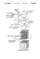
- FIG. 1is a block diagram of a processor array system
- FIG. 2is a perspective block diagram of a computer incorporating the processor array system of FIG. 1;
- FIG. 3is a dataflow diagram of the MCU;
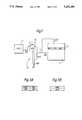
- FIGS. 3A and 3Bshow a 64-bit row in word mode and in row/column mode; and,
- FIG. 4is a diagram of an array support unit.
- a processor array systemcomprises a processor array 1, a scalar control unit (MCU) 2 and an array support unit 3.
- the array support unit 3includes an edge register ME and interface circuitry 4.
- the processor arraycomprises a two-dimensional array of single bit processing elements with the local store associated with each processing element providing a third addressable dimension.
- Such an arrayis described in British patent no. 1,445,714.
- the arrayis of dimensions 64 ⁇ 64, that is each row or column is 64 bits wide.
- the MCU 2 shown schematically in FIG. 3includes a 32-bit scalar processor which operates to control the instruction execution and addressing of the array 1.
- the output from the 32-bit scalar processoris taken via a 32-bit wide data bus to the MCU registers.
- fourteen such general purpose MCU registersare used. These registers hold address modifiers or codestore link values and can be operated upon by MCU arithmetic or logic functions. The contents of these registers may be transferred to or from the array via the interface circuitry 4 in the array support unit 3.
- the edge register MEsupplies data to and from the array via a 64-bit wide data bus 7.
- the edge register MEis used for such operations as extracting a row of data and replicating the row throughout the array. Apart from acting as a source or destination of data to or from the array the only other possible operation involving the edge register ME are shifting by one place or having its output tested by the function SKIP. Unlike the general purpose MCU registers the edge register ME cannot be used as a modifier.
- edge register METhere is no direct data path between the MCU and the edge register ME so that ME becomes undefined if specified as the result of MCU arithmetic or logical operations other than a shift of one place, in which case the edge register ME is both source and destination. Conversely if the edge register ME is specified as the source data for an MCU arithmetic logical or shift operation then the data used by the MCU operation is undefined.
- the MCUaddresses specified rows of the array.
- the 32-bit data words from the MCUare either zero extended at the most significant end and written to the specified row, producing a row in which the first half is null and the second half takes the values supplied by the MCU as seen in row R of the processor array 1 in FIG. 1, or alternatively the 32-bit data word from the MCU is replicated to fill the row in the manner shown in FIG. 3A.
- each 64-bit rowis divided into two 32-bit words.
- Data from the MCU registersare written to a selected word (i.e. part row or part column) of the array.
- edge register MEWhen the edge register ME is specified as the source of the data a 64-bit data word from the register ME is written to the array 1 to fill the specified row or column in the manner shown in FIG. 3B.
- edge register and MCU registersprovide different methods of writing data so there are corresponding methods of reading data from the array.
- the edge register and MCU registersprovide different methods of writing data so there are corresponding methods of reading data from the array.
- the least significant word of the edge-sized response from the arrayis sent to the MCU and the rest of the response discarded.
- bits from a specified word address within the specified row or columnare selected from the edge-sized response and sent to the MCU so again the rest of the response is discarded.
- the edge register MEis used and the edge-sized response transmitted whole to the register.
- the appropriate method of writing or reading data for a given operationis controlled by the MCU and appropriate control signals transmitted from the MCU to the array support unit 3.
- the array support unit 3is shown in detail in FIG. 4.
- Drivers D1-D7are provided in the interface circuit 4 and in the output paths from the edge register ME.
- each driverIn response to a signal at its enabling input 101-107 each driver outputs the 32 bit data word provided at its input.
- the data inputis fixed at logical zero: this driver is used to zero extent 32 bit words from the MCU.
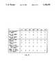
- the control signals supplied by the MCU to the enabling inputs 101-107 for the different addressing modesare shown in Table 1.
- the processor systemis controlled by a host processor connected via a host connection unit (HCU).
- HCUhost connection unit
- the HCUhas access to the array so that the host can address the array store as an extension of its own memory.
- the HCUaddresses the array using word addressing in a manner analogous to that used by the MCU registers to read from or write to specified words described above.
- the format of an array byte addressis therefore of the form:
- Aarray store bit-plane address
- Iarray, row or column number
- a 32-bit scalar MCUcan be used with a 128 ⁇ 128 array.
- the MCU dataflow and controlremains identical to that described above for the 32/64 ⁇ 64 bit system, it only being necessary to modify the array support unit 3 by replacing the 64-bit edge register with a 128-bit register and adapting the interface with the MCU registers. Only minor changes are necessary to the address generation in the MCU. Individual words within a row or column can be addressed in a manner precisely analogous to that described above for the 64-bit array but with four words to a row or column rather than merely two. An array address then takes the form:
Landscapes
- Engineering & Computer Science (AREA)
- Theoretical Computer Science (AREA)
- Computer Hardware Design (AREA)
- Physics & Mathematics (AREA)
- General Engineering & Computer Science (AREA)
- General Physics & Mathematics (AREA)
- Computing Systems (AREA)
- Multi Processors (AREA)
- Executing Machine-Instructions (AREA)
- Exchange Systems With Centralized Control (AREA)
- Electrotherapy Devices (AREA)
- Hardware Redundancy (AREA)
- Advance Control (AREA)
Abstract
Description
100A AAAA AAAA AAAA AAAA AAAI IIII IW. .
1AAA AAAA AAAA AAAA AAAA AIII IIII WW. .
Claims (4)
Applications Claiming Priority (2)
| Application Number | Priority Date | Filing Date | Title |
|---|---|---|---|
| GB8820237 | 1988-08-25 | ||
| GB888820237AGB8820237D0 (en) | 1988-08-25 | 1988-08-25 | Processor array systems |
Publications (1)
| Publication Number | Publication Date |
|---|---|
| US5150290Atrue US5150290A (en) | 1992-09-22 |
Family
ID=10642723
Family Applications (1)
| Application Number | Title | Priority Date | Filing Date |
|---|---|---|---|
| US07/397,709Expired - Fee RelatedUS5150290A (en) | 1988-08-25 | 1989-08-23 | Processor array system incorporating n-bit scalar processor and m x m-bit processor array |
Country Status (6)
| Country | Link |
|---|---|
| US (1) | US5150290A (en) |
| EP (1) | EP0357342B1 (en) |
| JP (1) | JPH02236790A (en) |
| AT (1) | ATE136381T1 (en) |
| DE (1) | DE68926136D1 (en) |
| GB (1) | GB8820237D0 (en) |
Cited By (10)
| Publication number | Priority date | Publication date | Assignee | Title |
|---|---|---|---|---|
| US5590356A (en)* | 1994-08-23 | 1996-12-31 | Massachusetts Institute Of Technology | Mesh parallel computer architecture apparatus and associated methods |
| US5864703A (en)* | 1997-10-09 | 1999-01-26 | Mips Technologies, Inc. | Method for providing extended precision in SIMD vector arithmetic operations |
| US6266758B1 (en) | 1997-10-09 | 2001-07-24 | Mips Technologies, Inc. | Alignment and ordering of vector elements for single instruction multiple data processing |
| US6298364B1 (en)* | 1993-03-08 | 2001-10-02 | Sharp Kabushiki Kaisha | Digital signal processing operation apparatus that allows combined operation |
| US6308252B1 (en)* | 1999-02-04 | 2001-10-23 | Kabushiki Kaisha Toshiba | Processor method and apparatus for performing single operand operation and multiple parallel operand operation |
| US20020116432A1 (en)* | 2001-02-21 | 2002-08-22 | Morten Strjbaek | Extended precision accumulator |
| US7197625B1 (en) | 1997-10-09 | 2007-03-27 | Mips Technologies, Inc. | Alignment and ordering of vector elements for single instruction multiple data processing |
| US7599981B2 (en) | 2001-02-21 | 2009-10-06 | Mips Technologies, Inc. | Binary polynomial multiplier |
| US7617388B2 (en) | 2001-02-21 | 2009-11-10 | Mips Technologies, Inc. | Virtual instruction expansion using parameter selector defining logic operation on parameters for template opcode substitution |
| US7711763B2 (en) | 2001-02-21 | 2010-05-04 | Mips Technologies, Inc. | Microprocessor instructions for performing polynomial arithmetic operations |
Families Citing this family (1)
| Publication number | Priority date | Publication date | Assignee | Title |
|---|---|---|---|---|
| US7536395B2 (en) | 2006-06-06 | 2009-05-19 | International Business Machines Corporation | Efficient dynamic register file design for multiple simultaneous bit encodings |
Citations (7)
| Publication number | Priority date | Publication date | Assignee | Title |
|---|---|---|---|---|
| US4101960A (en)* | 1977-03-29 | 1978-07-18 | Burroughs Corporation | Scientific processor |
| US4107773A (en)* | 1974-05-13 | 1978-08-15 | Texas Instruments Incorporated | Advanced array transform processor with fixed/floating point formats |
| US4365292A (en)* | 1979-11-26 | 1982-12-21 | Burroughs Corporation | Array processor architecture connection network |
| US4412303A (en)* | 1979-11-26 | 1983-10-25 | Burroughs Corporation | Array processor architecture |
| US4543642A (en)* | 1982-01-26 | 1985-09-24 | Hughes Aircraft Company | Data Exchange Subsystem for use in a modular array processor |
| US4720784A (en)* | 1983-10-18 | 1988-01-19 | Thiruvengadam Radhakrishnan | Multicomputer network |
| US4891787A (en)* | 1986-12-17 | 1990-01-02 | Massachusetts Institute Of Technology | Parallel processing system with processor array having SIMD/MIMD instruction processing |
Family Cites Families (3)
| Publication number | Priority date | Publication date | Assignee | Title |
|---|---|---|---|---|
| US3858183A (en)* | 1972-10-30 | 1974-12-31 | Amdahl Corp | Data processing system and method therefor |
| JPS5930156A (en)* | 1982-08-09 | 1984-02-17 | Sharp Corp | microcomputer system |
| US4783732A (en)* | 1985-12-12 | 1988-11-08 | Itt Corporation | Two-wire/three-port RAM for cellular array processor |
- 1988
- 1988-08-25GBGB888820237Apatent/GB8820237D0/enactivePending
- 1989
- 1989-08-23USUS07/397,709patent/US5150290A/ennot_activeExpired - Fee Related
- 1989-08-24EPEP89308611Apatent/EP0357342B1/ennot_activeExpired - Lifetime
- 1989-08-24DEDE68926136Tpatent/DE68926136D1/ennot_activeExpired - Lifetime
- 1989-08-24ATAT89308611Tpatent/ATE136381T1/enactive
- 1989-08-25JPJP1220121Apatent/JPH02236790A/enactivePending
Patent Citations (7)
| Publication number | Priority date | Publication date | Assignee | Title |
|---|---|---|---|---|
| US4107773A (en)* | 1974-05-13 | 1978-08-15 | Texas Instruments Incorporated | Advanced array transform processor with fixed/floating point formats |
| US4101960A (en)* | 1977-03-29 | 1978-07-18 | Burroughs Corporation | Scientific processor |
| US4365292A (en)* | 1979-11-26 | 1982-12-21 | Burroughs Corporation | Array processor architecture connection network |
| US4412303A (en)* | 1979-11-26 | 1983-10-25 | Burroughs Corporation | Array processor architecture |
| US4543642A (en)* | 1982-01-26 | 1985-09-24 | Hughes Aircraft Company | Data Exchange Subsystem for use in a modular array processor |
| US4720784A (en)* | 1983-10-18 | 1988-01-19 | Thiruvengadam Radhakrishnan | Multicomputer network |
| US4891787A (en)* | 1986-12-17 | 1990-01-02 | Massachusetts Institute Of Technology | Parallel processing system with processor array having SIMD/MIMD instruction processing |
Cited By (23)
| Publication number | Priority date | Publication date | Assignee | Title |
|---|---|---|---|---|
| US6298364B1 (en)* | 1993-03-08 | 2001-10-02 | Sharp Kabushiki Kaisha | Digital signal processing operation apparatus that allows combined operation |
| US5590356A (en)* | 1994-08-23 | 1996-12-31 | Massachusetts Institute Of Technology | Mesh parallel computer architecture apparatus and associated methods |
| US7197625B1 (en) | 1997-10-09 | 2007-03-27 | Mips Technologies, Inc. | Alignment and ordering of vector elements for single instruction multiple data processing |
| US7546443B2 (en) | 1997-10-09 | 2009-06-09 | Mips Technologies, Inc. | Providing extended precision in SIMD vector arithmetic operations |
| US8074058B2 (en) | 1997-10-09 | 2011-12-06 | Mips Technologies, Inc. | Providing extended precision in SIMD vector arithmetic operations |
| US20020062436A1 (en)* | 1997-10-09 | 2002-05-23 | Timothy J. Van Hook | Method for providing extended precision in simd vector arithmetic operations |
| US20110055497A1 (en)* | 1997-10-09 | 2011-03-03 | Mips Technologies, Inc. | Alignment and Ordering of Vector Elements for Single Instruction Multiple Data Processing |
| US7793077B2 (en) | 1997-10-09 | 2010-09-07 | Mips Technologies, Inc. | Alignment and ordering of vector elements for single instruction multiple data processing |
| US7159100B2 (en) | 1997-10-09 | 2007-01-02 | Mips Technologies, Inc. | Method for providing extended precision in SIMD vector arithmetic operations |
| US20090249039A1 (en)* | 1997-10-09 | 2009-10-01 | Mips Technologies, Inc. | Providing Extended Precision in SIMD Vector Arithmetic Operations |
| US5864703A (en)* | 1997-10-09 | 1999-01-26 | Mips Technologies, Inc. | Method for providing extended precision in SIMD vector arithmetic operations |
| US6266758B1 (en) | 1997-10-09 | 2001-07-24 | Mips Technologies, Inc. | Alignment and ordering of vector elements for single instruction multiple data processing |
| US20070250683A1 (en)* | 1997-10-09 | 2007-10-25 | Mips Technologies, Inc. | Alignment and ordering of vector elements for single instruction multiple data processing |
| US6308252B1 (en)* | 1999-02-04 | 2001-10-23 | Kabushiki Kaisha Toshiba | Processor method and apparatus for performing single operand operation and multiple parallel operand operation |
| US7225212B2 (en) | 2001-02-21 | 2007-05-29 | Mips Technologies, Inc. | Extended precision accumulator |
| US7181484B2 (en) | 2001-02-21 | 2007-02-20 | Mips Technologies, Inc. | Extended-precision accumulation of multiplier output |
| US7599981B2 (en) | 2001-02-21 | 2009-10-06 | Mips Technologies, Inc. | Binary polynomial multiplier |
| US7617388B2 (en) | 2001-02-21 | 2009-11-10 | Mips Technologies, Inc. | Virtual instruction expansion using parameter selector defining logic operation on parameters for template opcode substitution |
| US7711763B2 (en) | 2001-02-21 | 2010-05-04 | Mips Technologies, Inc. | Microprocessor instructions for performing polynomial arithmetic operations |
| US20020178203A1 (en)* | 2001-02-21 | 2002-11-28 | Mips Technologies, Inc., A Delaware Corporation | Extended precision accumulator |
| US7860911B2 (en) | 2001-02-21 | 2010-12-28 | Mips Technologies, Inc. | Extended precision accumulator |
| US20020116432A1 (en)* | 2001-02-21 | 2002-08-22 | Morten Strjbaek | Extended precision accumulator |
| US8447958B2 (en) | 2001-02-21 | 2013-05-21 | Bridge Crossing, Llc | Substituting portion of template instruction parameter with selected virtual instruction parameter |
Also Published As
| Publication number | Publication date |
|---|---|
| ATE136381T1 (en) | 1996-04-15 |
| EP0357342B1 (en) | 1996-04-03 |
| GB8820237D0 (en) | 1988-09-28 |
| DE68926136D1 (en) | 1996-05-09 |
| JPH02236790A (en) | 1990-09-19 |
| EP0357342A1 (en) | 1990-03-07 |
Similar Documents
| Publication | Publication Date | Title |
|---|---|---|
| US4467443A (en) | Bit addressable variable length memory system | |
| US4739474A (en) | Geometric-arithmetic parallel processor | |
| US5150290A (en) | Processor array system incorporating n-bit scalar processor and m x m-bit processor array | |
| US6041387A (en) | Apparatus for read/write-access to registers having register file architecture in a central processing unit | |
| EP0239119B1 (en) | Information transferring method and apparatus of transferring information from one memory area to another memory area | |
| US7571300B2 (en) | Modular distributive arithmetic logic unit | |
| EP1314099B1 (en) | Method and apparatus for connecting a massively parallel processor array to a memory array in a bit serial manner | |
| EP0377296B1 (en) | Cache coherency control when programmable option selection (POS) and memory expansion | |
| US6230238B1 (en) | Method and apparatus for accessing misaligned data from memory in an efficient manner | |
| US5603046A (en) | Method for complex data movement in a multi-processor data processing system | |
| US20040172517A1 (en) | Synchronous periodical orthogonal data converter | |
| US4811266A (en) | Multifunction arithmetic indicator | |
| US4277836A (en) | Composite random access memory providing direct and auxiliary memory access | |
| JPH01229378A (en) | image data storage device | |
| JP4482356B2 (en) | Image processing method and image processing apparatus using SIMD processor | |
| JP3837293B2 (en) | SIMD type microprocessor having constant selection function | |
| US5548771A (en) | Multi-processor data processing system having multiple ports coupled to multiple interface circuits | |
| US4775929A (en) | Time partitioned bus arrangement | |
| JP3014424B2 (en) | Test method for multiport memory | |
| US4916601A (en) | Means for transferring firmware signals between a control store and a microprocessor means through a reduced number of connections by transfer according to firmware signal function | |
| KR0172369B1 (en) | Semiconductor memory device | |
| JPH07168750A (en) | Information processor | |
| JP2004192405A (en) | SIMD type processor | |
| JPH02224041A (en) | Cache memory control circuit | |
| JP2512994B2 (en) | Vector register |
Legal Events
| Date | Code | Title | Description |
|---|---|---|---|
| AS | Assignment | Owner name:AMT (HOLDINGS) LTD., 65 SUTTONS PARK AVENUE, READI Free format text:ASSIGNMENT OF ASSIGNORS INTEREST.;ASSIGNOR:HUNT, DAVID J.;REEL/FRAME:005188/0764 Effective date:19891031 | |
| FEPP | Fee payment procedure | Free format text:PAYOR NUMBER ASSIGNED (ORIGINAL EVENT CODE: ASPN); ENTITY STATUS OF PATENT OWNER: LARGE ENTITY | |
| AS | Assignment | Owner name:OCHORIOS LIMITED, UNITED KINGDOM Free format text:ASSIGNMENT OF ASSIGNORS INTEREST;ASSIGNORS:AMT (HOLDINGS) LIMITED;ACTIVE MEMORY TECHNOLOGY LIMITED;REEL/FRAME:006528/0792 Effective date:19920731 Owner name:CAMBRIDGE PARALLEL PROCESSING LIMITED, UNITED KING Free format text:CHANGE OF NAME;ASSIGNORS:OCHORIOS LIMITED;CAMBRIDGE ACTIVE MEMORY TECHNOLOGY LIMITED;REEL/FRAME:006528/0789 Effective date:19930427 Owner name:CAMBRIDGE MANAGEMENT CORPORATION, CALIFORNIA Free format text:ASSIGNMENT OF ASSIGNORS INTEREST;ASSIGNOR:CAMBRIDGE PARALLEL PROCESSING LIMITED;REEL/FRAME:006531/0933 Effective date:19930413 | |
| FPAY | Fee payment | Year of fee payment:4 | |
| REMI | Maintenance fee reminder mailed | ||
| LAPS | Lapse for failure to pay maintenance fees | ||
| FP | Lapsed due to failure to pay maintenance fee | Effective date:20000922 | |
| STCH | Information on status: patent discontinuation | Free format text:PATENT EXPIRED DUE TO NONPAYMENT OF MAINTENANCE FEES UNDER 37 CFR 1.362 |