US5148503A - Apparatus and method for linearized cascade coupled integrated optical modulator - Google Patents
Apparatus and method for linearized cascade coupled integrated optical modulatorDownload PDFInfo
- Publication number
- US5148503A US5148503AUS07/706,911US70691191AUS5148503AUS 5148503 AUS5148503 AUS 5148503AUS 70691191 AUS70691191 AUS 70691191AUS 5148503 AUS5148503 AUS 5148503A
- Authority
- US
- United States
- Prior art keywords
- modulator
- output
- interferometric
- modulators
- coupler
- Prior art date
- Legal status (The legal status is an assumption and is not a legal conclusion. Google has not performed a legal analysis and makes no representation as to the accuracy of the status listed.)
- Expired - Lifetime
Links
- 230000003287optical effectEffects0.000titleclaimsdescription37
- 238000000034methodMethods0.000titleclaimsdescription13
- 239000000758substrateSubstances0.000claimsdescription22
- 230000008878couplingEffects0.000claimsdescription13
- 238000010168coupling processMethods0.000claimsdescription13
- 238000005859coupling reactionMethods0.000claimsdescription13
- 238000012546transferMethods0.000description9
- 239000004020conductorSubstances0.000description6
- 239000013078crystalSubstances0.000description6
- 239000000835fiberSubstances0.000description6
- 230000010287polarizationEffects0.000description5
- 230000005540biological transmissionEffects0.000description4
- 238000010586diagramMethods0.000description4
- 238000004891communicationMethods0.000description3
- 230000001629suppressionEffects0.000description3
- 238000003491arrayMethods0.000description2
- 230000006872improvementEffects0.000description2
- GQYHUHYESMUTHG-UHFFFAOYSA-Nlithium niobateChemical compound[Li+].[O-][Nb](=O)=OGQYHUHYESMUTHG-UHFFFAOYSA-N0.000description2
- 238000012986modificationMethods0.000description2
- 230000004048modificationEffects0.000description2
- 239000013307optical fiberSubstances0.000description2
- 239000010409thin filmSubstances0.000description2
- 206010070670Limb asymmetryDiseases0.000description1
- RTAQQCXQSZGOHL-UHFFFAOYSA-NTitaniumChemical compound[Ti]RTAQQCXQSZGOHL-UHFFFAOYSA-N0.000description1
- 238000004458analytical methodMethods0.000description1
- 230000008033biological extinctionEffects0.000description1
- 239000000969carrierSubstances0.000description1
- 230000008859changeEffects0.000description1
- 230000003247decreasing effectEffects0.000description1
- 230000001419dependent effectEffects0.000description1
- 230000000694effectsEffects0.000description1
- 230000005684electric fieldEffects0.000description1
- 238000005516engineering processMethods0.000description1
- 238000003475laminationMethods0.000description1
- 238000004519manufacturing processMethods0.000description1
- 229910052751metalInorganic materials0.000description1
- 239000002184metalSubstances0.000description1
- 238000012544monitoring processMethods0.000description1
- 239000000382optic materialSubstances0.000description1
- 229920000620organic polymerPolymers0.000description1
- 230000002441reversible effectEffects0.000description1
- 238000012552reviewMethods0.000description1
- 239000004065semiconductorSubstances0.000description1
- 230000035945sensitivityEffects0.000description1
- 230000001360synchronised effectEffects0.000description1
- 239000010936titaniumSubstances0.000description1
- 229910052719titaniumInorganic materials0.000description1
Images


Classifications
- G—PHYSICS
- G02—OPTICS
- G02F—OPTICAL DEVICES OR ARRANGEMENTS FOR THE CONTROL OF LIGHT BY MODIFICATION OF THE OPTICAL PROPERTIES OF THE MEDIA OF THE ELEMENTS INVOLVED THEREIN; NON-LINEAR OPTICS; FREQUENCY-CHANGING OF LIGHT; OPTICAL LOGIC ELEMENTS; OPTICAL ANALOGUE/DIGITAL CONVERTERS
- G02F1/00—Devices or arrangements for the control of the intensity, colour, phase, polarisation or direction of light arriving from an independent light source, e.g. switching, gating or modulating; Non-linear optics
- G02F1/01—Devices or arrangements for the control of the intensity, colour, phase, polarisation or direction of light arriving from an independent light source, e.g. switching, gating or modulating; Non-linear optics for the control of the intensity, phase, polarisation or colour
- G02F1/21—Devices or arrangements for the control of the intensity, colour, phase, polarisation or direction of light arriving from an independent light source, e.g. switching, gating or modulating; Non-linear optics for the control of the intensity, phase, polarisation or colour by interference
- G02F1/225—Devices or arrangements for the control of the intensity, colour, phase, polarisation or direction of light arriving from an independent light source, e.g. switching, gating or modulating; Non-linear optics for the control of the intensity, phase, polarisation or colour by interference in an optical waveguide structure
- G—PHYSICS
- G02—OPTICS
- G02F—OPTICAL DEVICES OR ARRANGEMENTS FOR THE CONTROL OF LIGHT BY MODIFICATION OF THE OPTICAL PROPERTIES OF THE MEDIA OF THE ELEMENTS INVOLVED THEREIN; NON-LINEAR OPTICS; FREQUENCY-CHANGING OF LIGHT; OPTICAL LOGIC ELEMENTS; OPTICAL ANALOGUE/DIGITAL CONVERTERS
- G02F1/00—Devices or arrangements for the control of the intensity, colour, phase, polarisation or direction of light arriving from an independent light source, e.g. switching, gating or modulating; Non-linear optics
- G02F1/29—Devices or arrangements for the control of the intensity, colour, phase, polarisation or direction of light arriving from an independent light source, e.g. switching, gating or modulating; Non-linear optics for the control of the position or the direction of light beams, i.e. deflection
- G02F1/31—Digital deflection, i.e. optical switching
- G02F1/313—Digital deflection, i.e. optical switching in an optical waveguide structure
- G02F1/3136—Digital deflection, i.e. optical switching in an optical waveguide structure of interferometric switch type
- G—PHYSICS
- G02—OPTICS
- G02F—OPTICAL DEVICES OR ARRANGEMENTS FOR THE CONTROL OF LIGHT BY MODIFICATION OF THE OPTICAL PROPERTIES OF THE MEDIA OF THE ELEMENTS INVOLVED THEREIN; NON-LINEAR OPTICS; FREQUENCY-CHANGING OF LIGHT; OPTICAL LOGIC ELEMENTS; OPTICAL ANALOGUE/DIGITAL CONVERTERS
- G02F2203/00—Function characteristic
- G02F2203/19—Function characteristic linearised modulation; reduction of harmonic distortions
Definitions
- This inventionrelates generally to modulators, and more particularly to a method and apparatus for the linearization of integrated electro-optical modulators.
- Integrated electro-optical modulatorsare finding increasing use in state-of-the-art analog optical-fiber communication systems. Such systems are being developed as an alternative to conventional electromagnetic transmission lines.
- Present optical-fiber communication systemsmay consist of a high power, low noise laser source in conjunction with a wide bandwidth external modulator, for example.
- a common problem in such systemsis that the dynamic range thereof is limited by intermodulation distortion, and by harmonic distortion due to modulator nonlinearities. Many attempts have been made in the art to improve the linearity of the modulators.
- One method of improving the linearity of optical modulatorsis to provide electromagnetic predistortion of the input signal.
- a system for accomplishing thisis reported in an article by R. P. Childs and D. A. O'Byrne, that appeared in OFC 90, entitled "Predistortion Linearization of Directly Modulated DFB Lasers and External Modulators for AM Video Transmission.”
- Johnson U.S. Pat. Nos. 5,015,053 and 5,002,355refer to linearization of an interferometric modulator by coupling to transverse electric (TE) and transverse magnetic (TM) modes.
- a carrier wave derived from a light sourceis polarized by a polarizer for adjusting the power of the carrier wave in the TE and TM polarization modes.
- Hamilton et al. U.S. Pat. No. 5,010,346shows an electro-optical analog-to-digital converter.
- a laser light sourceis synchronized with a digital clock for producing pulses of light.
- the pulses of lightare modulated by an optical modulator for varying the intensity of the pulses of light as a function of the amplitude of the analog modulating signal.
- the light pulsesare demultiplexed and passed through a detector for converting the light pulses to electrical signals.
- the electrical signalsare then passed through an electrical analog-to-digital converter.
- DuPuy et al U.S. Pat. No. 4,997,245shows optical switches that are polarization independent.
- the optical switchesinclude a substrate of electro-optic material in which waveguides are formed in a manner permitting light waves to be switched therethrough independent of polarization phenomena.
- Thylen U.S. Pat. No. 4,993,798refers to an optical communication system consisting of a semiconductor laser that includes an optical waveguide coupled at one end to first and second optical directional switches. The other ends of each one of the directional couplers each have an end of a waveguide terminated to a mirror, for forming a cavity including the laser diode. By either modulating current driving the diode, or by applying a modulating signal to the directional couplers, a light signal passing therethrough can be modulated.
- Yoon et al U.S. Pat. No. 4,936,645shows a polarization-insensitive Mach-Zehnder modulator that includes a thin film waveguide on a substrate.
- the modulatorconsists of a lamination of different organic polymers upon which the thin film waveguide is deposited, and electrodes for applying voltages for producing electric fields to coact with the light passing through the waveguides.
- Koai U.S. Pat. No. 4,934,776teaches the combination of cascaded individual waveguide directional coupler sections arranged to provide a high-density optical data array, for forming an integrated optical intensity modulator.
- the cascaded coupled-waveguide modulatorsprovide ultra-high extinction ratios.
- Koai U.S. Pat. No. 4,934,775shows an optical space-division switching architecture consisting of high-extinction electro-optical data arrays of a plurality of cascaded coupled-waveguide optical intensity modulators.
- a plurality of passive splitter circuitsare used to evenly divide an input optical signal into a plurality of interim optical signals.
- the optical signalsare passed through the optical intensity modulators, respectively, which have waveguide coupler sections cascaded together on a crystal substrate to form a bar-type modulator structure, for providing a direct optical connection between the various sections of each modulator.
- Combiner circuitsreceive the output optical signals from the data arrays and combine them for providing a single output wave or signal.
- Coleman U.S. Pat. No. 4,882,775shows a demodulator provided by an interferometer and a signal processor.
- the demodulatoris included in a coherence multiplexed, optical data transmission system.
- the optical data transmission systemincludes an interferometric modulator at an input end.
- the output signals therefromare modulated waveforms which are passed through an optical multiplexer, and coupled via single mode optical couplers and a fiber optic cable to demodulator stages.
- Each modulator and demodulator stageis provided by an unequal arm-length Mach-Zehnder interferometer.
- the multiplexersphase modulate the optical carriers from the modulators for multiplexing the same together.
- the path lengths between the modulators and demodulators included in the systemare controlled for obtaining a desired output from the output demodulator stages 40.
- U.S. Pat. No. 4,390,236shows an electro-optical demultiplexer consisting of a plurality of cascaded tunable, polarization independent optical wavelength filters.
- the various sections of the filters, as cascaded,provide an input polarization selective coupler that separates the transverse electrical (TE) and transverse magnetic (TM) orthogonally polarized wave components, respectively, of an arbitrarily polarized input signal.
- the separated TE and TM componentsthen travel along two different wavepaths or waveguides.
- Each waveguideincludes a wavelength selective mode converter.
- An output polarization selective coupleris provided for combining in one output waveguide signal components centered about the wavelength of the mode converters, and for combining in a second output waveguide the balance of the input signal.
- Papuchon U.S. Pat. No. 4,223,977shows an integrated optical circuit for separating a plurality of optical waves of different wavelengths, thereby providing a demultiplexing function.
- a plurality of basic electro-optical cellsare integrated on a single substrate for providing the optical demultiplexing circuit.
- a paper entitled "Waveguide Modulators with Extended Linear Dynamic Range a Theoretical Prediction”shows a modified-directional-coupler modulator with reduced nonlinear distortion.
- the couplerincludes an input stage for receiving input signals for a voltage control directional coupler that couples the signals to a Mach-Zehnder interferometer.
- the output of the interferometeris coupled by a fixed directional coupler to an output waveguide providing two channels. The parameters are adjusted for minimizing third order intermodulation spurious signals.
- a paper entitled "In Search of a Linear Electro-optic Amplitude Modulator"shows a linear electro-optic amplitude modulator.
- the modulatorincludes a Y-branch for dividing an optical input signal equally for inputting into the two arms, respectively, of a Mach-Zehnder interferometer.
- the interferometerfunctions as a phase shifter.
- the output of the interferometeris supplied to a directional coupler having a nominal coupling constant-length product of half a coupling length.
- the optical output signalis provided at each of two output waveguides.
- a modulation signal of one polarityis applied to the interferometer phase shifter, and is applied in reverse polarity to the directional coupler using a multiplication factor.
- the parametersare adjusted for optimizing the linearity of the modulator by reducing the second and third order harmonics that cause nonlinearities to occur.
- the present inventorrecognized that known integrated optics modulators require further improvement.
- One need recognizedis to improve the linearity of integrated optical modulators.
- An object of the present inventionis to provide an improved integrated optical modulator.
- Another object of the inventionis to provide an integrated optical modulator having increased linearity.
- an integrated optical modulatorhaving a plurality of cascaded stages of Mach-Zehnder type Y-branch configured interferometric modulators and coupler structure interferometric modulators.
- the amplitude of the modulating voltage applied to each stage, and the level of the DC bias applied to each stage,are adjusted for increasing the linearity of the modulated output signal.
- various ones of the stagesmay each be provided by a 2X1 interferometric switch.
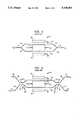
- FIG. 1is a simplified pictorial diagram of a known Y-branch interferometric modulator
- FIG. 2is a simplified pictorial diagram of a known coupler structure interferometric modulator
- FIG. 3is a simplified pictorial diagram of one embodiment of the invention.
- FIG. 4is a simplified pictorial diagram of another embodiment of the invention.
- FIG. 5is a pictorial view of another embodiment of the invention.
- FIG. 6is a curve of harmonic suppression plotted against a modulation index m, for a known interferometric modulator compared against an integrated interferometric modulator of one embodiment of the invention.
- FIG. 1a Y-branch electro-optical interferometric modulator 2 is shown.
- An input light wave P 0typically having a power level expressed in milliwatts, is applied to an input waveguide 4, for carrying the light wave P 0 to be divided into upper waveguide segment 6 and lower waveguide segment 8 of the Y-waveguide 4, 6, 8.
- Light from the upper segment 6travels through a longitudinal upper waveguide segment 10, through an upper waveguide segment 12, and through an output waveguide segment 14 for providing a portion of an output light signal P.sub.(t).
- a lower leg or waveguide segment 16forms a Y-branch with waveguide segments 14 and 16.
- Waveguide segment 16receives light from a lower longitudinal waveguide segment 18 at one end thereof, the other end of the latter being connected to receive light from an end of the lower waveguide segment 8.
- waveguide segments 4, 6, 10, 12 and 14form a continuous waveguide, as do waveguide segments 4, 8, 18, 16 and 14.
- An elongated relatively narrow metal electrode 20is positioned relatively close to the top of the upper longitudinal waveguide segment 10, with the longitudinal axis of each being parallel.
- Another electrode 22that is rectangular in shape, but substantially wider than electrode 20, in this example, is located between the upper and lower longitudinal waveguide segments 10 and 18 with its longitudinal axis parallel thereto.
- a third electrode 24 substantially identical in shape to electrode 20is located beneath waveguide segment 18, with the longitudinal axes of the two being parallel. Electrode 24 has substantially the same shape as electrode 20, with these electrodes and electrode 22 all being juxtaposed and in vertical alignment with one another, in this example.
- a modulating or instantaneous voltage V(t)is connected to electrode 22.
- the upper and lower electrodes 20 and 24are each connected to a source of reference potential, ground in this example.
- a DC bias voltage ⁇ 1is also connected to electrode 22.
- Electrodes 20, 22, and 24are deposited on top of the substrate 82. Note that the shape of any of the electrodes illustrated above are not meant to be limiting in that many shapes or configurations can be used for the electrodes.
- a light signal P 0 applied to input waveguide 4is substantially equally divided. One half portion travels through waveguide segments 6, 10, 12, and another half portion travels through waveguide segments 8, 16, and 18, as indicated above.
- Light traveling through waveguide segment 10passes between electrodes 20 and 22, and the light through waveguide segment 18 passes between electrodes 22 and 24.
- the modulating signal V(t)causes the index of refraction of the crystal substrate 82 to change for increasing the speed of light through waveguide 10, and decreasing the speed of light through waveguide 18, for example, in accordance with the instantaneous amplitude at any given time of the modulating signal V(t).
- the phase difference created between the light traveling through the upper waveguide 10 and lower waveguide 18modulates the light.
- the light from waveguide 10then travels through waveguide 12 to output waveguide 14, and light from waveguide 18 through waveguide 16 to waveguide 14, whereby the two portions of the original light signal P 0 are combined together to form the modulated output light signal P.sub.(t).
- the output light signal P.sub.(t)includes only the in-phase components of the modulated light, in that in a Y-branch modulator components of light that are in phase quadrature are absorbed in the crystal substrate 82, in this example.
- the known interferometric modulator of FIG. 1has the following transfer function:
- ⁇ (t)is proportional to the input signal voltage V(t), while ⁇ is proportional to the level of the DC bias voltage ⁇ 1 , in this example.
- FIG. 2Another known interferometric coupler structure for providing a Mach-Zehnder interferometric modulator 26 is shown in FIG. 2.
- the formerincludes waveguide coupling sections 28 and 30.
- a light wave P 0 signalis delivered to a lower input waveguide segment 32 that lies relatively in a substantially horizontal plane, with the light being conducted therefrom through an upward sloping waveguide segment 34, and therefrom through a lower horizontal waveguide segment 36 of a coupling section 28.
- a portion of the light traveling through the lower horizontal waveguide segment 36ideally has half of its light energy coupled into the upper horizontal waveguide portion 38 of coupler 28.
- the remaining light from waveguide 36then travels through the downward sloping waveguide section or segment 40, therefrom through the lower longitudinal waveguide segment 42, then through an upwardly sloping waveguide segment 44 and into a horizontal lower waveguide segment 46 of a second coupler 30.
- the latteralso includes an upper horizontal waveguide segment 48.
- Light coupled from lower horizontal waveguide segment 36 of coupler 28, coupled into the upper horizontal segment 38travels from the latter to an upwardly sloping waveguide segment 50, through an upper longitudinal waveguide segment 52, into a downwardly sloping waveguide segment 54, and therefrom into the upper horizontal waveguide segment 48 of coupler 46, where this light is combined with light coupled thereinto from the lower horizontal waveguide segment 46 of this coupler.
- Both the linear and nonlinear components of the light wave signals combined in waveguide segment 48travel therefrom through an upwardly sloping waveguide segment 56 to a horizontal waveguide segment 58, for outputting therefrom as an output light signal P.sub.(t), in this example.
- a relatively narrow rectangular electrode 60is positioned above the upper longitudinal waveguide segment 52, and a similar electrode 62 is positioned below lower longitudinal waveguide segment 42.
- a third electrode 64that is substantially wider than either of electrodes 60 and 62, in this example, is positioned between the upper and lower longitudinal waveguides 52, 42, respectively.
- the electrodes 60, 62, and 64are juxtaposed and substantially in alignment with one another.
- the lower waveguide segment 32has a corresponding upper waveguide segment 66 that continues into a downwardly sloping upper waveguide segment 68.
- the upper output waveguide segment 58has a corresponding lower waveguide segment 70, with the latter connecting with a downward sloping lower waveguide segment 72, as shown.
- the electrodescan have other configurations than those illustrated herein.
- the operation of the coupler structure interferometric modulator 26is similar to that of the Y-branch interferometric modulator 2 of FIG. 1. However unlike the latter which absorbs the phase quadrature components of the output wave form in the crystal substrate 82, the coupler structure modulator 26 does not absorb these phase quadrature components. Therefore, the coupler interferometric modulator 26 tends to provide a higher output light signal P.sub.(t).
- the transfer function for the coupler structure interferometric modulator 26can be the same as the Y-branch interferometric modulator 2, as given in equation (1) above. However, if the couplings 28 and 30 are varied, a slightly modified transfer function results as shown below in equation (2):
- ⁇ 2 (t)is the phase angle in radians and is proportional to signal voltage V(t)
- ⁇ 2is a phase angle representative of the DC bias applied to electrode 64, the DC bias being typically in units of volts
- cis a measure of the couplings 28 and 30, and is typically a complex number having no units, as is known in the art.
- the cosine expression including ⁇ 2 (t)is representative of a second order harmonic, with the following term being a third order harmonic, and so forth. If the bias voltage represented by the phase angle ⁇ , in this example, has a level of ⁇ /2, even order terms in equation (3) will vanish.
- the present inventorrecognized that compensation for nonlinearities due to second, third, and higher order harmonics can be obtained when suitable combinations of the transfer functions of equations 1 and 2 are implemented.
- the present inventionprovides such suitable combinations of these transfer functions by cascade coupling two or more interferometric modulators such as some combination of modulators 2 and 26 of FIGS. 1 and 2, respectively, whereby a total transfer function is obtained as shown below in equation (4):
- ⁇ 1n , ⁇ 2ndepends on the coupling C, ⁇ n (t) is proportional to V(t) but with n dependent proportionality constants (sensitivity).
- sensitivityn dependent proportionality constants
- a first stageis a Y-branch interferometric modulator 2
- a second stageis a coupler-structure interferometric modulator 26, as shown in FIG. 3.
- FIG. 3In another embodiment of the invention, as shown in FIG.
- the first stage or input stageis also a Y-branch interferometric modulator 2
- the second or output stageis shown as 2X1 switch or interferometric modulator 73 that includes a coupler input section 74 and a Y-branch output section 76, instead of a coupler output section 30 as in interferometric modulator 26.
- xk 1 ⁇ V(t)
- k 1is a proportionality constant referring to voltage and phase
- C1is related to coupling 28
- C2is related to coupling 30
- kis representative of a ratio between the voltage applied to the second stage (26 or 72) versus the voltage applied to the first stage 2 of the cascaded interferometric modulators of FIGS. 3 or 4.
- C1equals 1.0
- C 1can be greater than 1.0, whereby the latter embodiment yields a slightly better light throughput than the embodiment of FIG. 4.
- a linearized interferometric modulatorcan be provided by cascading some combination of a plurality of the modulator configurations 2, 26, and 73, or 2 and 26, or 2 and 73, or 26 and 73, or all of one type, for example.
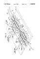
- FIG. 5a simplified pictorial illustration is shown of a two-stage cascaded integrated optical modulator 80 that includes a substrate 82 of lithium niobate crystal, for example.
- Interferometric modulatorssubstantially similar to modulators 2 and 26 of FIG. 3 are formed in cascade on the substrate.
- a substantially U-shaped electrode 84provides electrode 24 at its base, and electrode 20 in two inwardly projecting segments from the upper portions of arms 86 and 88.
- the ends of arms 86 and 88terminate to connector or terminal pads 90 and 92 for connection via conductors 94 and 96, respectively, to ground pads 98 and 100 of an auxiliary printed circuit (PC) board 102, as shown.
- the U-shaped electrode 84is formed on top of the substrate 82 over the waveguide segments 6, 8, 12, and 16, as shown.
- Center electrode 22is formed by a shortened T-like electrode configuration having a terminal pad 102 for connection via a conductor 104 to a conductor 106 on PC board 102, for receiving an input voltage signal V(t), and a DC bias voltage ⁇ 1 , in this example.
- a fiber optic cable 108is coupled via a fiber cable-to-substrate attachment 110 to an end of input waveguide segment 4 of modulator 2, for delivering a light signal thereto.
- the electrodes for modulator 26are provided from a relatively U-shaped electrode 112 formed on top of the substrate 82 as shown, for providing electrode 62 at its base, and electrodes 60 from stub-like inwardly projecting electrode portions from the upper ends of the electrode arms 114 and 116.
- the ends of arms 114 and 116terminate to connecting pads 118 and 120, respectively, for connection via conductors 122 and 124 to ground pads 126 and 128 formed on PC board 102 as shown.
- the center electrode 64is formed on top of the substrate 82 in a substantially stub-like T-configuration, as shown, where the leg of the T-configuration terminates to a connection pad 130 for connection via a conductor 132 to an end of conductor strip 134 on PC board 102, for receiving an input signal k ⁇ V(t) and a DC bias ⁇ 2 .
- a light fiber cable 136is connected via a fiber cable-to-substrate attachment or connector 110 to the end of output waveguide segment 70, for receiving the primary light output signal P.sub.(t).
- another fiber optic cable 138is connected via a connector 110 to the end of waveguide 58.
- waveguide segments 6, 10, and 12may be taken jointly as providing an upper waveguide forming a continuous waveguide with input segment 4 and output segment 14; and waveguide segments 8, 18, and 16 may be taken as a continuous lower waveguide in conjunction with input waveguide segment 4 and output waveguide segment 14.
- waveguide segments 50, 52, and 54 of modulator 26form a continuous upper waveguide, whereas waveguide segments 40, 42, and 44 form a continuous lower waveguide.
- the cascaded interferometric modulator of FIG. 5operates generally as described for the substantially similar configuration of FIG. 3. More specifically, the Y-branch interferometric modulator 2 modulates the light input signal P 0 in a nonlinear manner, causing the output light waveform provided in waveguide segment 14 to be nonlinear, typically approximating a cosine function. This modulated output signal is then conducted via waveguide segment 34 into the coupler switch interferometric modulator 26, for modulating the light wave by a modulating voltage kV(t), as shown in FIG. 5.
- the ultimate modulated light output signal P.sub.(t) delivered to output waveguide segment 70is a product of the modulation of the input light wave signal P 0 by both modulators 2 and 26.
- Modulator 26also modulates light signals in a nonlinear manner.
- level of the DC bias ⁇ 1 applied to modulator 2and the DC bias ⁇ 2 applied to modulator 26, it is possible to obtain cancellation or minimize the product terms, as previously described.
- modulating voltage V(t) applied to modulator 2and k ⁇ V(t) applied to interferometric modulator 26, along with adjustment of the previously mentioned DC biases, but primarily by adjustment of the DC biases, certain of the product terms can be effectively zeroed out.
- a two-stage cascaded interferometric modulator using the configuration of FIG. 4is similarly fabricated as the integrated modulator 80 of FIG. 5, the former may require different levels of DC biasing voltages and a different ratio k between the modulating voltages, in order to optimize the linearity of the resultant output signal P.sub.(t).
- the embodiment of FIGS. 3 and 5is preferred, in that the embodiment of FIG. 4 includes a Y-branch in the output stage 72 that tends to absorb components of light in phase quadrature, whereas the output stage 26 of the embodiments of FIGS. 3 and 5 does not absorb light, thereby permitting more light to pass through.
- the DC bias voltages ⁇ 1 and ⁇ 2are shown applied in combination with respective modulating voltages to inner electrode 22 of modulator 2, and inner electrode 64 of modulator 26, respectively.
- the DC bias voltages ⁇ 1 and ⁇ 2may be applied to modulators 2 and 26 through separate and independent terminal pads and electrodes independent of the modulating voltage input connections.
- the fabrication of such an alternately configured cascaded modulator device, however,may be more complicated than that of FIG. 5.
- the harmonic suppressionis plotted against the modulation index m, with the former being given in dB.
- Curve 140shows the third harmonic generation for a single element interferometric modulator.
- Curve 142shows the second harmonic generation for a cascaded interferometric modulator 80, and curve 144 shows the third harmonic generation for the latter.
- n stages of such modulators 2, 26, and 72can be cascaded together in some predetermined combination for providing a minimization of nonlinearities, to in effect maximize the linearity of the modulated output signal P.sub.(t).
- the objectiveis to cancel or substantially reduce harmonics in P.sub.(t).
- modulator 26can serve as the input stage, and modulator 2 as an output stage.
- modulator 73can serve as the input stage, and modulator 2 as the output stage.
Landscapes
- Physics & Mathematics (AREA)
- Nonlinear Science (AREA)
- General Physics & Mathematics (AREA)
- Optics & Photonics (AREA)
- Optical Modulation, Optical Deflection, Nonlinear Optics, Optical Demodulation, Optical Logic Elements (AREA)
- Optical Integrated Circuits (AREA)
Abstract
Description
P.sub.(t) =Po/2[1+cos(φ(t)+α)] (1)
(2) P.sub.2(t) =1/2(1+c).[1-(1-c)/(1+c) cos (φ.sub.2 (t)+α.sub.2)](2)
P.sub.(t) ≈Po/2 [1+cos α-sin α. φ(t)-1/2 cos α. φ.sup.2 (t)+1/6 sin α. φ.sup.3 (t)+higher order terms] (3)
P.sub.(t) =Po/2 [1+cos (φ.sub.1 (t)+α.sub.1)]Γ.sub.11 [1+Γ.sub.21 cos (φ.sub.2 (t)+α.sub.2)]. . . Γ.sub.1n [1+Γ.sub.2n cos (φ.sub.n (t)+α.sub.n)] (4)
φ.sub.1 (t)=k.sub.1 V(t) (5)
φ.sub.n (t)=k.sub.n V(t) (6)
P(V.sub.(t))=P(o)+P'(o)·V.sub.(t) +1/2P"(o)·V.sup.2 (t)+1/6 P'"(O)·V.sup.3 (t) . . . +1/n!P.sup.(n) (O)·V.sup.n (t) (7)
P.sup.(n) =d.sup.n P/(dV).sup.n (8)
P(t)=P.sub.o /4 (1-sin (x+α.sub.1))·C.sub.1 ·[1+C.sub.2 sin (kx+α.sub.2)] (9)
α.sub.1 =0 (10)
d.sup.2 P(t)/dx.sup.2 =0 and (11)
d.sup.3 P(t)/dx.sup.3 =0 (12)
tan α.sub.2 =-2/k (13)
C2=√(4+k.sup.2)/(k.sup.4 +6k.sup.2 +2) (14)
Claims (23)
Priority Applications (4)
| Application Number | Priority Date | Filing Date | Title |
|---|---|---|---|
| US07/706,911US5148503A (en) | 1991-05-29 | 1991-05-29 | Apparatus and method for linearized cascade coupled integrated optical modulator |
| EP92108878AEP0516064B1 (en) | 1991-05-29 | 1992-05-26 | Integrated optical modulator and method of providing a linearly modulated light signal |
| DE69214879TDE69214879T2 (en) | 1991-05-29 | 1992-05-26 | Integrated optical modulator and method for providing a linearly modulated light signal |
| JP4160323AJPH05210073A (en) | 1991-05-29 | 1992-05-27 | Integrated electro-optic modulator and its linearity enhancement method |
Applications Claiming Priority (1)
| Application Number | Priority Date | Filing Date | Title |
|---|---|---|---|
| US07/706,911US5148503A (en) | 1991-05-29 | 1991-05-29 | Apparatus and method for linearized cascade coupled integrated optical modulator |
Publications (1)
| Publication Number | Publication Date |
|---|---|
| US5148503Atrue US5148503A (en) | 1992-09-15 |
Family
ID=24839586
Family Applications (1)
| Application Number | Title | Priority Date | Filing Date |
|---|---|---|---|
| US07/706,911Expired - LifetimeUS5148503A (en) | 1991-05-29 | 1991-05-29 | Apparatus and method for linearized cascade coupled integrated optical modulator |
Country Status (4)
| Country | Link |
|---|---|
| US (1) | US5148503A (en) |
| EP (1) | EP0516064B1 (en) |
| JP (1) | JPH05210073A (en) |
| DE (1) | DE69214879T2 (en) |
Cited By (69)
| Publication number | Priority date | Publication date | Assignee | Title |
|---|---|---|---|---|
| US5249243A (en)* | 1992-05-21 | 1993-09-28 | Siemens Components, Inc. | Apparatus and method for cascade coupled integrated optical phase modulator for linearization of signal transfer |
| US5278923A (en)* | 1992-09-02 | 1994-01-11 | Harmonic Lightwaves, Inc. | Cascaded optical modulation system with high linearity |
| US5323406A (en)* | 1992-11-02 | 1994-06-21 | Yee Ting K | Photonic mixer for photonically multiplying two electrical signals in two optically interconnected interferometric modulators operated at modulation outside the linear range |
| US5339369A (en)* | 1992-10-23 | 1994-08-16 | General Microwave Israel Corporation | High-speed external modulator |
| US5347601A (en)* | 1993-03-29 | 1994-09-13 | United Technologies Corporation | Integrated optical receiver/transmitter |
| US5363230A (en)* | 1991-12-20 | 1994-11-08 | Telefonaktiebolaget L M Ericsson | Method of linearizing the transmission function of modulator |
| US5455876A (en)* | 1992-10-23 | 1995-10-03 | General Microwave Israel Corporation | High-speed external integrated optical modulator |
| US5515195A (en)* | 1993-06-25 | 1996-05-07 | Optivision Incorporated | Optical bus using controllable optical devices |
| US5546484A (en)* | 1994-10-14 | 1996-08-13 | Kaptron, Inc. | Fiber optic switch using polished-type directional coupler |
| WO1996042027A1 (en)* | 1995-06-09 | 1996-12-27 | Corning Incorporated | Mach-zehnder switch |
| US5594818A (en)* | 1995-03-08 | 1997-01-14 | Lucent Technologies Inc. | Digital optical switch and modulator and a method for digital optical switching and modulation |
| US5615037A (en)* | 1995-01-17 | 1997-03-25 | Massachusetts Institute Of Technology | Sub-octave bandpass optical remote antenna link modulator and method therefor |
| WO1997037278A1 (en)* | 1996-03-29 | 1997-10-09 | Crystal Technology, Inc. | Linearized optic modulator with segmented electrodes |
| US5703975A (en)* | 1995-06-09 | 1997-12-30 | Corning Incorporated | Interferometric switch |
| US5710653A (en)* | 1995-03-06 | 1998-01-20 | Fiber Optic Network Solutions Corp. | Linear multi-output optical transmitter system |
| US5875048A (en)* | 1995-03-06 | 1999-02-23 | Cfx Communication Systems,Llc | Linear multi-output optical transmitter system |
| US5915052A (en)* | 1997-06-30 | 1999-06-22 | Uniphase Telecommunications Products, Inc. | Loop status monitor for determining the amplitude of the signal components of a multi-wavelength optical beam |
| US5953139A (en)* | 1996-03-06 | 1999-09-14 | Cfx Communications Systems, Llc | Wavelength division multiplexing system |
| US5955875A (en)* | 1997-01-31 | 1999-09-21 | Massachusetts Institute Of Technology | Linearized optical sampler |
| US5982964A (en)* | 1997-06-30 | 1999-11-09 | Uniphase Corporation | Process for fabrication and independent tuning of multiple integrated optical directional couplers on a single substrate |
| US6020986A (en)* | 1997-11-21 | 2000-02-01 | Jds Uniphase Corporation | Programmable add-drop module for use in an optical circuit |
| US6031849A (en)* | 1997-11-14 | 2000-02-29 | Jds Uniphase Corporation | High power three level fiber laser and method of making same |
| US6091864A (en)* | 1997-04-10 | 2000-07-18 | Ortel Corporation | Linear optical modulator for providing chirp-free optical signals |
| US6151157A (en)* | 1997-06-30 | 2000-11-21 | Uniphase Telecommunications Products, Inc. | Dynamic optical amplifier |
| US6204951B1 (en) | 1997-05-21 | 2001-03-20 | Keotrel Solutions, Inc. | Electro-optic modulator with improved harmonic performance |
| US6226424B1 (en) | 1997-09-19 | 2001-05-01 | Uniphase Telecommunications Products, Inc. | Integrated wavelength-select transmitter |
| US6236771B1 (en)* | 1999-01-13 | 2001-05-22 | Hitachi, Ltd. | Optical transmission apparatus |
| US6240232B1 (en)* | 1996-03-29 | 2001-05-29 | Siemens Aktiengesellschaft | Process for the production of a waveguide beam converter |
| US6341031B1 (en) | 1999-05-25 | 2002-01-22 | Jds Uniphase Corporation | Optical pulse generation using a high order function waveguide interferometer |
| US6469649B1 (en) | 2000-03-08 | 2002-10-22 | Massachusetts Institute Of Technology | Narrowband analog to digital converter with suppressed second-order distortion |
| WO2003012535A1 (en)* | 2001-07-27 | 2003-02-13 | Axe, Inc. | Optical pulse generator with single frequency drive |
| US20030077054A1 (en)* | 2001-10-23 | 2003-04-24 | Marco Marazzi | Optical devices for communication |
| US20030147591A1 (en)* | 2002-02-07 | 2003-08-07 | Fujitsu Limited | Optical waveguide device and optical modulator |
| US20040008395A1 (en)* | 2000-11-22 | 2004-01-15 | Jds Uniphase Corporation | Cascaded RZ and NRZ laser modulators having RZ/NRZ phase alignment bias control |
| WO2004032385A1 (en) | 2002-10-03 | 2004-04-15 | Nortel Networks Limited | Optical dispersion compensation in the electrical domain in an optical communications system |
| US6781537B1 (en) | 2003-06-10 | 2004-08-24 | Nortel Networks Limited | High speed digital to analog converter |
| US20040197103A1 (en)* | 2002-10-03 | 2004-10-07 | Nortel Networks Limited | Electrical domain compensation of non-linear effects in an optical communications system |
| US20040240765A1 (en)* | 2003-05-30 | 2004-12-02 | Jds Uniphase Corporation | Optical digital external modulator |
| US20050007642A1 (en)* | 2002-12-02 | 2005-01-13 | Nortel Networks Limited | Optical E-field modulation using a Mach-Zehnder interferometer |
| US6943931B1 (en) | 2004-06-02 | 2005-09-13 | Benjamin Dingel | Ultra-high linearized optical modulator |
| US20050213863A1 (en)* | 2003-01-30 | 2005-09-29 | Fujitsu Limited | Optical modulator |
| US20060077401A1 (en)* | 2004-09-27 | 2006-04-13 | Manish Kothari | Measurement of the dynamic characteristics of interferometric modulators |
| US20060127102A1 (en)* | 2004-12-10 | 2006-06-15 | Nortel Networks Limited | Modulation E-field based control of a non-linear transmitter |
| US20070092262A1 (en)* | 2005-10-25 | 2007-04-26 | Donald Bozarth | Adaptive optical transmitter for use with externally modulated lasers |
| US7212326B2 (en) | 2003-05-30 | 2007-05-01 | Jds Uniphase Corporation | Optical external modulator |
| US20070134006A1 (en)* | 2005-12-12 | 2007-06-14 | Eric Krieg | Method for adjusting bias in optical transmitter with external modulator |
| US7266306B1 (en) | 2003-10-03 | 2007-09-04 | Nortel Networks Limited | Method for optical carrier suppression and quadrature control |
| WO2007123551A1 (en)* | 2006-04-26 | 2007-11-01 | Georgia Tech Research Corporation | High speed optical switch |
| WO2008005061A1 (en) | 2006-06-30 | 2008-01-10 | Lucent Technologies Inc. | Optical modulator |
| US7321734B2 (en) | 2004-07-29 | 2008-01-22 | Nortel Networks Limited | Digital synthesis of readily compensated optical signals |
| US7382985B2 (en) | 2002-12-02 | 2008-06-03 | Nortel Networks Limited | Electrical domain mitigation of polarization dependent effects in an optical communications system |
| US20090232518A1 (en)* | 2005-10-25 | 2009-09-17 | Emcore Corporation | Optical transmitter with adaptively controlled optically linearized modulator |
| US20090238510A1 (en)* | 2005-08-31 | 2009-09-24 | Tetsuya Kawanishi | Optical amplitude modulation system capable of cancelling high order component |
| US7672595B1 (en) | 2003-12-23 | 2010-03-02 | Nortel Networks Limited | Optical transmission system architecture supporting migration to electronic compensation of link impairments |
| US7680420B1 (en) | 2003-10-03 | 2010-03-16 | Nortel Networks Limited | Optical E-field modulation using a directly driven laser |
| US20100202723A1 (en)* | 2009-02-10 | 2010-08-12 | Fujitsu Limited | Optical modulator |
| US7787778B2 (en) | 2004-12-10 | 2010-08-31 | Ciena Corporation | Control system for a polar optical transmitter |
| US20110158576A1 (en)* | 2009-12-30 | 2011-06-30 | Jds Uniphase Corporation | Optical waveguide modulator |
| US20140286647A1 (en)* | 2013-03-19 | 2014-09-25 | Luxtera, Inc. | Method And System For A Low-Voltage Integrated Silicon High-Speed Modulator |
| US20150063809A1 (en)* | 2013-08-29 | 2015-03-05 | Fujitsu Optical Components Limited | Optical module and optical transmitter |
| US20150078763A1 (en)* | 2013-09-13 | 2015-03-19 | Fujitsu Optical Components Limited | Optical module and optical transmitter |
| US20170123239A1 (en)* | 2013-03-19 | 2017-05-04 | Luxtera, Inc. | Method And System For A Low-Voltage Integrated Silicon High-Speed Modulator |
| CN111555806A (en)* | 2015-03-20 | 2020-08-18 | 日本电气株式会社 | Pluggable optical module, communication system and communication method of pluggable optical module |
| US11032628B2 (en) | 2019-07-19 | 2021-06-08 | Lawrence Livermore National Security, Llc | Electronic demodulation of optically phase demodulated signals |
| US11159241B2 (en) | 2019-07-18 | 2021-10-26 | Lawrence Livermore National Security, Llc | High power handling digitizer using photonics |
| US20210349262A1 (en)* | 2020-05-07 | 2021-11-11 | Honeywell International Inc. | Integrated environmentally insensitive modulator for interferometric gyroscopes |
| US11184087B2 (en) | 2019-08-08 | 2021-11-23 | Lawrence Livermore National Security, Llc | Optical encoder devices and systems |
| US11209714B2 (en) | 2019-07-17 | 2021-12-28 | Lawrence Livermore National Security, Llc | Radio frequency passband signal generation using photonics |
| US11444690B2 (en) | 2019-07-17 | 2022-09-13 | Lawrence Livermore National Security, Llc | Timing measurement apparatus |
Families Citing this family (4)
| Publication number | Priority date | Publication date | Assignee | Title |
|---|---|---|---|---|
| US6304695B1 (en)* | 1999-05-17 | 2001-10-16 | Chiaro Networks Ltd. | Modulated light source |
| DE102004005716A1 (en)* | 2004-02-05 | 2005-06-23 | Siemens Ag | Mach-Zehnder-modulator for use as multiplexer, has optical conductors acting as phase modulators to change phases of signal components, where modulator is suitably triggered to deliver two data signals as one multiplexed signal at output |
| DE102004012060A1 (en)* | 2004-03-11 | 2005-09-08 | Siemens Ag | Optical time multiplexed signal multiplexer has Mach-Zehnder Modulator with high data rate inputs and lower frequency modulation control signals |
| JP2006276323A (en)* | 2005-03-29 | 2006-10-12 | Furukawa Electric Co Ltd:The | Light switch |
Citations (13)
| Publication number | Priority date | Publication date | Assignee | Title |
|---|---|---|---|---|
| US4223977A (en)* | 1978-04-25 | 1980-09-23 | Thomson-Csf | Integrated optical demultiplexing circuit |
| US4390236A (en)* | 1981-03-19 | 1983-06-28 | Bell Telephone Laboratories, Incorporated | Tunable polarization independent wavelength filter |
| US4882775A (en)* | 1988-07-22 | 1989-11-21 | The Boeing Company | Demodulation technique for coherence multiplexed optical data transmission system |
| US4932736A (en)* | 1989-09-29 | 1990-06-12 | Gte Laboratories Incorporated | High-extinction 1×2 integrated optical switch |
| US4934776A (en)* | 1988-12-23 | 1990-06-19 | Gte Laboratories Incorporated | Ultra-high-extinction cascaded coupled-waveguide optical modulators and optical gate arrays |
| US4934775A (en)* | 1989-01-18 | 1990-06-19 | Gte Laboratories Incorporated | Optical space switches using cascaded coupled-waveguide optical gate arrays |
| US4936645A (en)* | 1989-08-24 | 1990-06-26 | Hoechst Celanese Corp. | Waveguide electrooptic light modulator with low optical loss |
| US4947170A (en)* | 1988-06-22 | 1990-08-07 | The Boeing Company | All optical analog-to-digital converter |
| US4993798A (en)* | 1988-10-21 | 1991-02-19 | Telefonaktiebolaget L M Ericsson | Laser arrangement in optical communication system |
| US4997245A (en)* | 1990-01-04 | 1991-03-05 | Smiths Industries Aerospace & Defense Systems Incorporated | Polarization independent optical switches |
| US5002353A (en)* | 1989-04-25 | 1991-03-26 | Massachusetts Institute Of Technology | Apparatus and method for reducing modulator nonlinearities |
| US5010346A (en)* | 1989-10-27 | 1991-04-23 | The Boeing Company | Electro-optical analog-to-digital converter and method for digitizing an analog signal |
| US5015053A (en)* | 1989-04-25 | 1991-05-14 | Massachusetts Institute Of Technology | Reduction of modulator non-linearities with independent bias angle control |
- 1991
- 1991-05-29USUS07/706,911patent/US5148503A/ennot_activeExpired - Lifetime
- 1992
- 1992-05-26DEDE69214879Tpatent/DE69214879T2/ennot_activeExpired - Fee Related
- 1992-05-26EPEP92108878Apatent/EP0516064B1/ennot_activeExpired - Lifetime
- 1992-05-27JPJP4160323Apatent/JPH05210073A/enactivePending
Patent Citations (13)
| Publication number | Priority date | Publication date | Assignee | Title |
|---|---|---|---|---|
| US4223977A (en)* | 1978-04-25 | 1980-09-23 | Thomson-Csf | Integrated optical demultiplexing circuit |
| US4390236A (en)* | 1981-03-19 | 1983-06-28 | Bell Telephone Laboratories, Incorporated | Tunable polarization independent wavelength filter |
| US4947170A (en)* | 1988-06-22 | 1990-08-07 | The Boeing Company | All optical analog-to-digital converter |
| US4882775A (en)* | 1988-07-22 | 1989-11-21 | The Boeing Company | Demodulation technique for coherence multiplexed optical data transmission system |
| US4993798A (en)* | 1988-10-21 | 1991-02-19 | Telefonaktiebolaget L M Ericsson | Laser arrangement in optical communication system |
| US4934776A (en)* | 1988-12-23 | 1990-06-19 | Gte Laboratories Incorporated | Ultra-high-extinction cascaded coupled-waveguide optical modulators and optical gate arrays |
| US4934775A (en)* | 1989-01-18 | 1990-06-19 | Gte Laboratories Incorporated | Optical space switches using cascaded coupled-waveguide optical gate arrays |
| US5002353A (en)* | 1989-04-25 | 1991-03-26 | Massachusetts Institute Of Technology | Apparatus and method for reducing modulator nonlinearities |
| US5015053A (en)* | 1989-04-25 | 1991-05-14 | Massachusetts Institute Of Technology | Reduction of modulator non-linearities with independent bias angle control |
| US4936645A (en)* | 1989-08-24 | 1990-06-26 | Hoechst Celanese Corp. | Waveguide electrooptic light modulator with low optical loss |
| US4932736A (en)* | 1989-09-29 | 1990-06-12 | Gte Laboratories Incorporated | High-extinction 1×2 integrated optical switch |
| US5010346A (en)* | 1989-10-27 | 1991-04-23 | The Boeing Company | Electro-optical analog-to-digital converter and method for digitizing an analog signal |
| US4997245A (en)* | 1990-01-04 | 1991-03-05 | Smiths Industries Aerospace & Defense Systems Incorporated | Polarization independent optical switches |
Non-Patent Citations (6)
| Title |
|---|
| Pao Lo Liu, B. J. Li, and Y. S. Trisno, In Search of a Linear Electro optic Amplitude Modulator , SPIE Conference, 1990.* |
| Pao-Lo Liu, B. J. Li, and Y. S. Trisno, "In Search of a Linear Electro-optic Amplitude Modulator", SPIE Conference, 1990. |
| R. D. Childs and D. A. O Byrne, Predistortion Linearization of Directly Modulated DFB Lasers and External Modulators for AM Video Transmission , OFC 90, 1990* |
| R. D. Childs and D. A. O'Byrne, "Predistortion Linearization of Directly Modulated DFB Lasers and External Modulators for AM Video Transmission", OFC 90, 1990 |
| Z. Q. Lin and W. S. C. Chang, "Waveguide Modulators with Extended Linear Dynamic Range a Theoretical Prediction", Photonics Technology Letters, vol. 2, No. 12, Dec. '90. |
| Z. Q. Lin and W. S. C. Chang, Waveguide Modulators with Extended Linear Dynamic Range a Theoretical Prediction , Photonics Technology Letters, vol. 2, No. 12, Dec. 90.* |
Cited By (111)
| Publication number | Priority date | Publication date | Assignee | Title |
|---|---|---|---|---|
| US5363230A (en)* | 1991-12-20 | 1994-11-08 | Telefonaktiebolaget L M Ericsson | Method of linearizing the transmission function of modulator |
| US5249243A (en)* | 1992-05-21 | 1993-09-28 | Siemens Components, Inc. | Apparatus and method for cascade coupled integrated optical phase modulator for linearization of signal transfer |
| US5278923A (en)* | 1992-09-02 | 1994-01-11 | Harmonic Lightwaves, Inc. | Cascaded optical modulation system with high linearity |
| US5339369A (en)* | 1992-10-23 | 1994-08-16 | General Microwave Israel Corporation | High-speed external modulator |
| US5455876A (en)* | 1992-10-23 | 1995-10-03 | General Microwave Israel Corporation | High-speed external integrated optical modulator |
| US5323406A (en)* | 1992-11-02 | 1994-06-21 | Yee Ting K | Photonic mixer for photonically multiplying two electrical signals in two optically interconnected interferometric modulators operated at modulation outside the linear range |
| US5347601A (en)* | 1993-03-29 | 1994-09-13 | United Technologies Corporation | Integrated optical receiver/transmitter |
| US5515195A (en)* | 1993-06-25 | 1996-05-07 | Optivision Incorporated | Optical bus using controllable optical devices |
| US5546484A (en)* | 1994-10-14 | 1996-08-13 | Kaptron, Inc. | Fiber optic switch using polished-type directional coupler |
| US5615037A (en)* | 1995-01-17 | 1997-03-25 | Massachusetts Institute Of Technology | Sub-octave bandpass optical remote antenna link modulator and method therefor |
| US5867295A (en)* | 1995-01-17 | 1999-02-02 | Massachusetts Institute Of Technology | Sub-octave bandpass optical remote antenna link modulator and method therefor |
| US5710653A (en)* | 1995-03-06 | 1998-01-20 | Fiber Optic Network Solutions Corp. | Linear multi-output optical transmitter system |
| US5875048A (en)* | 1995-03-06 | 1999-02-23 | Cfx Communication Systems,Llc | Linear multi-output optical transmitter system |
| US6163395A (en)* | 1995-03-06 | 2000-12-19 | Fiber Optics Network Solutions Corp. | Linear multi-output optical transmitter system |
| US5594818A (en)* | 1995-03-08 | 1997-01-14 | Lucent Technologies Inc. | Digital optical switch and modulator and a method for digital optical switching and modulation |
| US5703975A (en)* | 1995-06-09 | 1997-12-30 | Corning Incorporated | Interferometric switch |
| WO1996042027A1 (en)* | 1995-06-09 | 1996-12-27 | Corning Incorporated | Mach-zehnder switch |
| US5953139A (en)* | 1996-03-06 | 1999-09-14 | Cfx Communications Systems, Llc | Wavelength division multiplexing system |
| US6240232B1 (en)* | 1996-03-29 | 2001-05-29 | Siemens Aktiengesellschaft | Process for the production of a waveguide beam converter |
| WO1997037278A1 (en)* | 1996-03-29 | 1997-10-09 | Crystal Technology, Inc. | Linearized optic modulator with segmented electrodes |
| US6028424A (en)* | 1997-01-31 | 2000-02-22 | Massachuetts Institute Of Technology | Linearized optical sampler |
| US5955875A (en)* | 1997-01-31 | 1999-09-21 | Massachusetts Institute Of Technology | Linearized optical sampler |
| US6091864A (en)* | 1997-04-10 | 2000-07-18 | Ortel Corporation | Linear optical modulator for providing chirp-free optical signals |
| US6204951B1 (en) | 1997-05-21 | 2001-03-20 | Keotrel Solutions, Inc. | Electro-optic modulator with improved harmonic performance |
| US6151157A (en)* | 1997-06-30 | 2000-11-21 | Uniphase Telecommunications Products, Inc. | Dynamic optical amplifier |
| US5982964A (en)* | 1997-06-30 | 1999-11-09 | Uniphase Corporation | Process for fabrication and independent tuning of multiple integrated optical directional couplers on a single substrate |
| US5915052A (en)* | 1997-06-30 | 1999-06-22 | Uniphase Telecommunications Products, Inc. | Loop status monitor for determining the amplitude of the signal components of a multi-wavelength optical beam |
| US6226424B1 (en) | 1997-09-19 | 2001-05-01 | Uniphase Telecommunications Products, Inc. | Integrated wavelength-select transmitter |
| US6370290B1 (en) | 1997-09-19 | 2002-04-09 | Uniphase Corporation | Integrated wavelength-select transmitter |
| US6031849A (en)* | 1997-11-14 | 2000-02-29 | Jds Uniphase Corporation | High power three level fiber laser and method of making same |
| US6020986A (en)* | 1997-11-21 | 2000-02-01 | Jds Uniphase Corporation | Programmable add-drop module for use in an optical circuit |
| US6236771B1 (en)* | 1999-01-13 | 2001-05-22 | Hitachi, Ltd. | Optical transmission apparatus |
| US6341031B1 (en) | 1999-05-25 | 2002-01-22 | Jds Uniphase Corporation | Optical pulse generation using a high order function waveguide interferometer |
| US6469649B1 (en) | 2000-03-08 | 2002-10-22 | Massachusetts Institute Of Technology | Narrowband analog to digital converter with suppressed second-order distortion |
| US6917455B2 (en) | 2000-11-22 | 2005-07-12 | Jds Uniphase Corporation | Cascaded RZ and NRZ laser modulators having RZ/NRZ phase alignment bias control |
| US20040008395A1 (en)* | 2000-11-22 | 2004-01-15 | Jds Uniphase Corporation | Cascaded RZ and NRZ laser modulators having RZ/NRZ phase alignment bias control |
| WO2003012535A1 (en)* | 2001-07-27 | 2003-02-13 | Axe, Inc. | Optical pulse generator with single frequency drive |
| US20030077054A1 (en)* | 2001-10-23 | 2003-04-24 | Marco Marazzi | Optical devices for communication |
| US20030147591A1 (en)* | 2002-02-07 | 2003-08-07 | Fujitsu Limited | Optical waveguide device and optical modulator |
| US7340114B2 (en)* | 2002-02-07 | 2008-03-04 | Fujitsu Limited | Optical waveguide device and optical modulator |
| WO2004032385A1 (en) | 2002-10-03 | 2004-04-15 | Nortel Networks Limited | Optical dispersion compensation in the electrical domain in an optical communications system |
| US9853725B2 (en) | 2002-10-03 | 2017-12-26 | Ciena Corporation | Optical dispersion compensation in the electrical domain in an optical communications system |
| US7376358B2 (en) | 2002-10-03 | 2008-05-20 | Nortel Networks Limited | Location specific optical monitoring |
| US20050008364A1 (en)* | 2002-10-03 | 2005-01-13 | Nortel Networks Limited | Location specific optical monitoring |
| US20040197103A1 (en)* | 2002-10-03 | 2004-10-07 | Nortel Networks Limited | Electrical domain compensation of non-linear effects in an optical communications system |
| US10574352B2 (en) | 2002-10-03 | 2020-02-25 | Ciena Corporation | Compensation of transmitter or receiver defects in an optical communications system |
| US9559778B2 (en) | 2002-10-03 | 2017-01-31 | Ciena Corporation | Optical dispersion compensation in the electrical domain in an optical communications system |
| US7756421B2 (en) | 2002-10-03 | 2010-07-13 | Ciena Corporation | Electrical domain compensation of non-linear effects in an optical communications system |
| EP3211809A1 (en) | 2002-10-03 | 2017-08-30 | Ciena Luxembourg S.a.r.l. | Optical dispersion compensation in the electrical domain in an optical communications system |
| US10164707B2 (en) | 2002-10-03 | 2018-12-25 | Ciena Corporation | Optical dispersion compensation in the electrical domain in an optical communications system |
| US7382984B2 (en) | 2002-10-03 | 2008-06-03 | Nortel Networks Limited | Electrical domain compensation of optical dispersion in an optical communications system |
| US7023601B2 (en) | 2002-12-02 | 2006-04-04 | Nortel Networks Limited | Optical E-field modulation using a Mach-Zehnder interferometer |
| US7382985B2 (en) | 2002-12-02 | 2008-06-03 | Nortel Networks Limited | Electrical domain mitigation of polarization dependent effects in an optical communications system |
| US20050007642A1 (en)* | 2002-12-02 | 2005-01-13 | Nortel Networks Limited | Optical E-field modulation using a Mach-Zehnder interferometer |
| US7155072B2 (en)* | 2003-01-30 | 2006-12-26 | Fujitsu Limited | Optical modulator |
| US20050213863A1 (en)* | 2003-01-30 | 2005-09-29 | Fujitsu Limited | Optical modulator |
| US7212326B2 (en) | 2003-05-30 | 2007-05-01 | Jds Uniphase Corporation | Optical external modulator |
| US6961166B2 (en) | 2003-05-30 | 2005-11-01 | Jds Uniphase Corporation | Optical digital external modulator |
| US20040240765A1 (en)* | 2003-05-30 | 2004-12-02 | Jds Uniphase Corporation | Optical digital external modulator |
| US6781537B1 (en) | 2003-06-10 | 2004-08-24 | Nortel Networks Limited | High speed digital to analog converter |
| US7266306B1 (en) | 2003-10-03 | 2007-09-04 | Nortel Networks Limited | Method for optical carrier suppression and quadrature control |
| US7680420B1 (en) | 2003-10-03 | 2010-03-16 | Nortel Networks Limited | Optical E-field modulation using a directly driven laser |
| US7672595B1 (en) | 2003-12-23 | 2010-03-02 | Nortel Networks Limited | Optical transmission system architecture supporting migration to electronic compensation of link impairments |
| US6943931B1 (en) | 2004-06-02 | 2005-09-13 | Benjamin Dingel | Ultra-high linearized optical modulator |
| US7321734B2 (en) | 2004-07-29 | 2008-01-22 | Nortel Networks Limited | Digital synthesis of readily compensated optical signals |
| US7453579B2 (en)* | 2004-09-27 | 2008-11-18 | Idc, Llc | Measurement of the dynamic characteristics of interferometric modulators |
| US20060077401A1 (en)* | 2004-09-27 | 2006-04-13 | Manish Kothari | Measurement of the dynamic characteristics of interferometric modulators |
| US7787778B2 (en) | 2004-12-10 | 2010-08-31 | Ciena Corporation | Control system for a polar optical transmitter |
| US7676161B2 (en) | 2004-12-10 | 2010-03-09 | Nortel Networks Limited | Modulation E-field based control of a non-linear transmitter |
| US20060127102A1 (en)* | 2004-12-10 | 2006-06-15 | Nortel Networks Limited | Modulation E-field based control of a non-linear transmitter |
| US20090238510A1 (en)* | 2005-08-31 | 2009-09-24 | Tetsuya Kawanishi | Optical amplitude modulation system capable of cancelling high order component |
| US7711215B2 (en)* | 2005-08-31 | 2010-05-04 | National Institute Of Information And Communications Technology | Optical amplitude modulation system capable of cancelling high order component |
| US20090232518A1 (en)* | 2005-10-25 | 2009-09-17 | Emcore Corporation | Optical transmitter with adaptively controlled optically linearized modulator |
| US8532499B2 (en) | 2005-10-25 | 2013-09-10 | Emcore Corporation | Optical transmitter with adaptively controlled optically linearized modulator |
| US20070092262A1 (en)* | 2005-10-25 | 2007-04-26 | Donald Bozarth | Adaptive optical transmitter for use with externally modulated lasers |
| US7853155B2 (en) | 2005-12-12 | 2010-12-14 | Emcore Corporation | Method for adjusting bias in optical transmitter with external modulator |
| US20070134006A1 (en)* | 2005-12-12 | 2007-06-14 | Eric Krieg | Method for adjusting bias in optical transmitter with external modulator |
| WO2007123551A1 (en)* | 2006-04-26 | 2007-11-01 | Georgia Tech Research Corporation | High speed optical switch |
| US20090214151A1 (en)* | 2006-04-26 | 2009-08-27 | Georgia Tech Research Corporation | High Speed Optical Switch |
| WO2008005061A1 (en) | 2006-06-30 | 2008-01-10 | Lucent Technologies Inc. | Optical modulator |
| US8135242B2 (en)* | 2009-02-10 | 2012-03-13 | Fujitsu Limited | Optical modulator |
| US20100202723A1 (en)* | 2009-02-10 | 2010-08-12 | Fujitsu Limited | Optical modulator |
| US8849071B2 (en) | 2009-12-30 | 2014-09-30 | Jds Uniphase Corporation | Optical waveguide modulator |
| US20110158576A1 (en)* | 2009-12-30 | 2011-06-30 | Jds Uniphase Corporation | Optical waveguide modulator |
| US9541775B2 (en)* | 2013-03-19 | 2017-01-10 | Luxtera, Inc. | Method and system for a low-voltage integrated silicon high-speed modulator |
| US11106061B2 (en) | 2013-03-19 | 2021-08-31 | Luxtera Llc | Method and system for a low-voltage integrated silicon high-speed modulator |
| US20170123239A1 (en)* | 2013-03-19 | 2017-05-04 | Luxtera, Inc. | Method And System For A Low-Voltage Integrated Silicon High-Speed Modulator |
| US10048518B2 (en)* | 2013-03-19 | 2018-08-14 | Luxtera, Inc. | Method and system for a low-voltage integrated silicon high-speed modulator |
| US20140286647A1 (en)* | 2013-03-19 | 2014-09-25 | Luxtera, Inc. | Method And System For A Low-Voltage Integrated Silicon High-Speed Modulator |
| US10613358B2 (en) | 2013-03-19 | 2020-04-07 | Luxtera, Inc. | Method and system for a low-voltage integrated silicon high-speed modulator |
| US9231728B2 (en)* | 2013-08-29 | 2016-01-05 | Fujitsu Optical Components Limited | Optical module and optical transmitter |
| US20150063809A1 (en)* | 2013-08-29 | 2015-03-05 | Fujitsu Optical Components Limited | Optical module and optical transmitter |
| US20150078763A1 (en)* | 2013-09-13 | 2015-03-19 | Fujitsu Optical Components Limited | Optical module and optical transmitter |
| US9229292B2 (en)* | 2013-09-13 | 2016-01-05 | Fujitsu Optical Components Limited | Optical module and optical transmitter |
| CN111555806A (en)* | 2015-03-20 | 2020-08-18 | 日本电气株式会社 | Pluggable optical module, communication system and communication method of pluggable optical module |
| US11921398B2 (en) | 2015-03-20 | 2024-03-05 | Nec Corporation | Pluggable optical module, optical communication system and control method of pluggable optical module |
| CN111555806B (en)* | 2015-03-20 | 2023-07-07 | 日本电气株式会社 | Pluggable optical module, communication system and communication method of pluggable optical module |
| US12003272B2 (en) | 2019-07-17 | 2024-06-04 | Lawrence Livermore National Security, Llc | Timing measurement apparatus |
| US11209714B2 (en) | 2019-07-17 | 2021-12-28 | Lawrence Livermore National Security, Llc | Radio frequency passband signal generation using photonics |
| US11444690B2 (en) | 2019-07-17 | 2022-09-13 | Lawrence Livermore National Security, Llc | Timing measurement apparatus |
| US11630368B2 (en) | 2019-07-17 | 2023-04-18 | Lawrence Livermore National Security, Llc | Radio frequency passband signal generation using photonics |
| US11159241B2 (en) | 2019-07-18 | 2021-10-26 | Lawrence Livermore National Security, Llc | High power handling digitizer using photonics |
| US11923907B2 (en) | 2019-07-18 | 2024-03-05 | Lawrence Livermore National Security, Llc | High power handling digitizer using photonics |
| US11032628B2 (en) | 2019-07-19 | 2021-06-08 | Lawrence Livermore National Security, Llc | Electronic demodulation of optically phase demodulated signals |
| US11575438B2 (en) | 2019-08-08 | 2023-02-07 | Lawrence Livermore National Security, Llc | Optical encoder devices and systems |
| US11184087B2 (en) | 2019-08-08 | 2021-11-23 | Lawrence Livermore National Security, Llc | Optical encoder devices and systems |
| US11996889B2 (en) | 2019-08-08 | 2024-05-28 | Lawrence Livermore National Security, Llc | Optical encoder devices and systems |
| US20220229231A1 (en)* | 2020-05-07 | 2022-07-21 | Honeywell International Inc. | Integrated environmentally insensitive modulator for interferometric gyroscopes |
| US11880067B2 (en)* | 2020-05-07 | 2024-01-23 | Honeywell International Inc. | Integrated environmentally insensitive modulator for interferometric gyroscopes |
| US11294120B2 (en)* | 2020-05-07 | 2022-04-05 | Honeywell International Inc. | Integrated environmentally insensitive modulator for interferometric gyroscopes |
| US20210349262A1 (en)* | 2020-05-07 | 2021-11-11 | Honeywell International Inc. | Integrated environmentally insensitive modulator for interferometric gyroscopes |
Also Published As
| Publication number | Publication date |
|---|---|
| EP0516064B1 (en) | 1996-10-30 |
| DE69214879D1 (en) | 1996-12-05 |
| DE69214879T2 (en) | 1997-04-10 |
| JPH05210073A (en) | 1993-08-20 |
| EP0516064A2 (en) | 1992-12-02 |
| EP0516064A3 (en) | 1993-04-07 |
Similar Documents
| Publication | Publication Date | Title |
|---|---|---|
| US5148503A (en) | Apparatus and method for linearized cascade coupled integrated optical modulator | |
| US5249243A (en) | Apparatus and method for cascade coupled integrated optical phase modulator for linearization of signal transfer | |
| JP2698797B2 (en) | External modulation method and apparatus for optical carrier | |
| US5835212A (en) | Variable chirp optical modulator using single modulation source | |
| EP0081177B1 (en) | Polarization-insensitive optical switch and multiplexing apparatus | |
| US12253786B2 (en) | Integrated electro-optic frequency comb generator | |
| Patel et al. | Liquid crystal and grating-based multiple-wavelength cross-connect switch | |
| US5168534A (en) | Cascaded optic modulator arrangement | |
| US5031235A (en) | Cable system incorporating highly linear optical modulator | |
| US6493473B1 (en) | Method and apparatus for providing transformation of the polarization of light | |
| US6943931B1 (en) | Ultra-high linearized optical modulator | |
| US5040865A (en) | Frequency multiplying electro-optic modulator configuration and method | |
| US5734493A (en) | Optical frequency conversion device | |
| US6483953B1 (en) | External optical modulation using non-co-linear compensation networks | |
| US20030190107A1 (en) | Optical modulator with pre-determined frequency chirp | |
| US5708734A (en) | Polarisation-independent optical device | |
| US5323406A (en) | Photonic mixer for photonically multiplying two electrical signals in two optically interconnected interferometric modulators operated at modulation outside the linear range | |
| JPH08500683A (en) | High linearity cascaded optical modulation system | |
| Tavlykaev et al. | Highly linear Y-fed directional coupler modulator with low intermodulation distortion | |
| GB2262162A (en) | Optical coupler | |
| US5230028A (en) | Electro-optic intensity modulator with improved linearity | |
| WO1991010297A1 (en) | Linear broadband signal generator using primary and secondary optical modulators | |
| US5125049A (en) | Multipurpose component with integrated optics and distribution network with optical amplification | |
| US20170214471A1 (en) | Multi-Bit Digital to Analog-Optical Converter | |
| GB2370369A (en) | Optical modulators |
Legal Events
| Date | Code | Title | Description |
|---|---|---|---|
| AS | Assignment | Owner name:CRYSTAL TECHNOLOGY, INC. A CORP. OF DELAWARE, CA Free format text:ASSIGNMENT OF ASSIGNORS INTEREST.;ASSIGNOR:SKEIE, HALVOR;REEL/FRAME:005813/0345 Effective date:19910802 | |
| STCF | Information on status: patent grant | Free format text:PATENTED CASE | |
| CC | Certificate of correction | ||
| FEPP | Fee payment procedure | Free format text:PAYOR NUMBER ASSIGNED (ORIGINAL EVENT CODE: ASPN); ENTITY STATUS OF PATENT OWNER: LARGE ENTITY | |
| FPAY | Fee payment | Year of fee payment:4 | |
| AS | Assignment | Owner name:UNIPHASE CORPORATION, CALIFORNIA Free format text:ASSIGNMENT OF ASSIGNORS INTEREST;ASSIGNOR:CRYSTAL TECHNOLOGY, INC.;REEL/FRAME:008861/0172 Effective date:19970926 Owner name:UNIPHASE TELECOMMUNICATIONS PRODUCTS, INC., CONNEC Free format text:ASSIGNMENT OF ASSIGNORS INTEREST;ASSIGNOR:UNIPHASE CORPORATION;REEL/FRAME:008861/0176 Effective date:19971027 | |
| FEPP | Fee payment procedure | Free format text:PAYER NUMBER DE-ASSIGNED (ORIGINAL EVENT CODE: RMPN); ENTITY STATUS OF PATENT OWNER: LARGE ENTITY | |
| FPAY | Fee payment | Year of fee payment:8 | |
| AS | Assignment | Owner name:JDS UNIPHASE CORPORATION, CALIFORNIA Free format text:ASSIGNMENT OF ASSIGNORS INTEREST;ASSIGNOR:UNIPHASE TELECOMMUNICATIONS PRODUCTS, INC.;REEL/FRAME:013295/0189 Effective date:20020815 | |
| FPAY | Fee payment | Year of fee payment:12 | |
| FEPP | Fee payment procedure | Free format text:PAYOR NUMBER ASSIGNED (ORIGINAL EVENT CODE: ASPN); ENTITY STATUS OF PATENT OWNER: LARGE ENTITY |