US5148265A - Semiconductor chip assemblies with fan-in leads - Google Patents
Semiconductor chip assemblies with fan-in leadsDownload PDFInfo
- Publication number
- US5148265A US5148265AUS07/673,020US67302091AUS5148265AUS 5148265 AUS5148265 AUS 5148265AUS 67302091 AUS67302091 AUS 67302091AUS 5148265 AUS5148265 AUS 5148265A
- Authority
- US
- United States
- Prior art keywords
- chip
- interposer
- terminals
- central
- assembly
- Prior art date
- Legal status (The legal status is an assumption and is not a legal conclusion. Google has not performed a legal analysis and makes no representation as to the accuracy of the status listed.)
- Expired - Lifetime
Links
- 239000004065semiconductorSubstances0.000titleclaimsabstractdescription23
- 230000000712assemblyEffects0.000titleclaimsdescription34
- 238000000429assemblyMethods0.000titleclaimsdescription34
- 230000002093peripheral effectEffects0.000claimsabstractdescription117
- 239000000758substrateSubstances0.000claimsabstractdescription86
- 238000012360testing methodMethods0.000claimsabstractdescription27
- 229910000679solderInorganic materials0.000claimsabstractdescription14
- 230000033001locomotionEffects0.000claimsabstractdescription13
- 239000008393encapsulating agentSubstances0.000claimsdescription29
- 239000000463materialSubstances0.000claimsdescription27
- 239000000523sampleSubstances0.000claimsdescription22
- 239000004020conductorSubstances0.000claimsdescription16
- 239000013536elastomeric materialSubstances0.000claimsdescription2
- 229920001169thermoplasticPolymers0.000claimsdescription2
- 229920001187thermosetting polymerPolymers0.000claimsdescription2
- 239000006260foamSubstances0.000claims1
- 238000000034methodMethods0.000abstractdescription38
- 241001296096ProblesSpecies0.000abstract1
- 230000008569processEffects0.000description14
- 238000005530etchingMethods0.000description13
- 238000004519manufacturing processMethods0.000description8
- 229920002120photoresistant polymerPolymers0.000description6
- 230000035882stressEffects0.000description6
- 238000000151depositionMethods0.000description5
- 229920001971elastomerPolymers0.000description5
- 229910052751metalInorganic materials0.000description5
- 239000002184metalSubstances0.000description5
- 239000002131composite materialSubstances0.000description4
- 230000001934delayEffects0.000description4
- 239000000806elastomerSubstances0.000description4
- 238000012545processingMethods0.000description4
- 238000005382thermal cyclingMethods0.000description4
- RYGMFSIKBFXOCR-UHFFFAOYSA-NCopperChemical compound[Cu]RYGMFSIKBFXOCR-UHFFFAOYSA-N0.000description3
- 239000000853adhesiveSubstances0.000description3
- 230000001070adhesive effectEffects0.000description3
- 238000013459approachMethods0.000description3
- 230000006835compressionEffects0.000description3
- 238000007906compressionMethods0.000description3
- 229910052802copperInorganic materials0.000description3
- 239000010949copperSubstances0.000description3
- 238000004049embossingMethods0.000description3
- 230000015654memoryEffects0.000description3
- 230000008646thermal stressEffects0.000description3
- 238000005452bendingMethods0.000description2
- 230000005540biological transmissionEffects0.000description2
- 239000003989dielectric materialSubstances0.000description2
- 230000006870functionEffects0.000description2
- 239000007769metal materialSubstances0.000description2
- 229910000510noble metalInorganic materials0.000description2
- 229920000642polymerPolymers0.000description2
- 230000002787reinforcementEffects0.000description2
- 229920002379silicone rubberPolymers0.000description2
- 239000002699waste materialSubstances0.000description2
- 229910000881Cu alloyInorganic materials0.000description1
- 239000004642PolyimideSubstances0.000description1
- 230000009471actionEffects0.000description1
- 229910045601alloyInorganic materials0.000description1
- 239000000956alloySubstances0.000description1
- 239000000919ceramicSubstances0.000description1
- 230000008859changeEffects0.000description1
- 238000000576coating methodMethods0.000description1
- 238000007796conventional methodMethods0.000description1
- 230000001351cycling effectEffects0.000description1
- 238000006073displacement reactionMethods0.000description1
- 238000004100electronic packagingMethods0.000description1
- 238000005538encapsulationMethods0.000description1
- 238000005516engineering processMethods0.000description1
- 230000009969flowable effectEffects0.000description1
- 229920002313fluoropolymerPolymers0.000description1
- 239000004811fluoropolymerSubstances0.000description1
- 238000010438heat treatmentMethods0.000description1
- 238000001746injection mouldingMethods0.000description1
- 239000007788liquidSubstances0.000description1
- 230000013011matingEffects0.000description1
- 239000012811non-conductive materialSubstances0.000description1
- 229920001721polyimidePolymers0.000description1
- 230000002035prolonged effectEffects0.000description1
- 238000004080punchingMethods0.000description1
- 230000005855radiationEffects0.000description1
- 230000000717retained effectEffects0.000description1
- 238000012216screeningMethods0.000description1
- 230000008054signal transmissionEffects0.000description1
- 239000004945silicone rubberSubstances0.000description1
- 239000007787solidSubstances0.000description1
- 239000000243solutionSubstances0.000description1
- 239000012899standard injectionSubstances0.000description1
- 238000005406washingMethods0.000description1
Images


Classifications
- H—ELECTRICITY
- H01—ELECTRIC ELEMENTS
- H01L—SEMICONDUCTOR DEVICES NOT COVERED BY CLASS H10
- H01L21/00—Processes or apparatus adapted for the manufacture or treatment of semiconductor or solid state devices or of parts thereof
- H01L21/67—Apparatus specially adapted for handling semiconductor or electric solid state devices during manufacture or treatment thereof; Apparatus specially adapted for handling wafers during manufacture or treatment of semiconductor or electric solid state devices or components ; Apparatus not specifically provided for elsewhere
- H01L21/683—Apparatus specially adapted for handling semiconductor or electric solid state devices during manufacture or treatment thereof; Apparatus specially adapted for handling wafers during manufacture or treatment of semiconductor or electric solid state devices or components ; Apparatus not specifically provided for elsewhere for supporting or gripping
- H01L21/6835—Apparatus specially adapted for handling semiconductor or electric solid state devices during manufacture or treatment thereof; Apparatus specially adapted for handling wafers during manufacture or treatment of semiconductor or electric solid state devices or components ; Apparatus not specifically provided for elsewhere for supporting or gripping using temporarily an auxiliary support
- H01L21/6836—Wafer tapes, e.g. grinding or dicing support tapes
- H—ELECTRICITY
- H01—ELECTRIC ELEMENTS
- H01L—SEMICONDUCTOR DEVICES NOT COVERED BY CLASS H10
- H01L22/00—Testing or measuring during manufacture or treatment; Reliability measurements, i.e. testing of parts without further processing to modify the parts as such; Structural arrangements therefor
- H01L22/30—Structural arrangements specially adapted for testing or measuring during manufacture or treatment, or specially adapted for reliability measurements
- H01L22/32—Additional lead-in metallisation on a device or substrate, e.g. additional pads or pad portions, lines in the scribe line, sacrificed conductors
- H—ELECTRICITY
- H01—ELECTRIC ELEMENTS
- H01L—SEMICONDUCTOR DEVICES NOT COVERED BY CLASS H10
- H01L23/00—Details of semiconductor or other solid state devices
- H01L23/12—Mountings, e.g. non-detachable insulating substrates
- H01L23/13—Mountings, e.g. non-detachable insulating substrates characterised by the shape
- H—ELECTRICITY
- H01—ELECTRIC ELEMENTS
- H01L—SEMICONDUCTOR DEVICES NOT COVERED BY CLASS H10
- H01L23/00—Details of semiconductor or other solid state devices
- H01L23/28—Encapsulations, e.g. encapsulating layers, coatings, e.g. for protection
- H01L23/31—Encapsulations, e.g. encapsulating layers, coatings, e.g. for protection characterised by the arrangement or shape
- H01L23/3107—Encapsulations, e.g. encapsulating layers, coatings, e.g. for protection characterised by the arrangement or shape the device being completely enclosed
- H—ELECTRICITY
- H01—ELECTRIC ELEMENTS
- H01L—SEMICONDUCTOR DEVICES NOT COVERED BY CLASS H10
- H01L23/00—Details of semiconductor or other solid state devices
- H01L23/28—Encapsulations, e.g. encapsulating layers, coatings, e.g. for protection
- H01L23/31—Encapsulations, e.g. encapsulating layers, coatings, e.g. for protection characterised by the arrangement or shape
- H01L23/3157—Partial encapsulation or coating
- H01L23/3164—Partial encapsulation or coating the coating being a foil
- H—ELECTRICITY
- H01—ELECTRIC ELEMENTS
- H01L—SEMICONDUCTOR DEVICES NOT COVERED BY CLASS H10
- H01L23/00—Details of semiconductor or other solid state devices
- H01L23/48—Arrangements for conducting electric current to or from the solid state body in operation, e.g. leads, terminal arrangements ; Selection of materials therefor
- H01L23/488—Arrangements for conducting electric current to or from the solid state body in operation, e.g. leads, terminal arrangements ; Selection of materials therefor consisting of soldered or bonded constructions
- H01L23/498—Leads, i.e. metallisations or lead-frames on insulating substrates, e.g. chip carriers
- H01L23/49805—Leads, i.e. metallisations or lead-frames on insulating substrates, e.g. chip carriers the leads being also applied on the sidewalls or the bottom of the substrate, e.g. leadless packages for surface mounting
- H—ELECTRICITY
- H01—ELECTRIC ELEMENTS
- H01L—SEMICONDUCTOR DEVICES NOT COVERED BY CLASS H10
- H01L23/00—Details of semiconductor or other solid state devices
- H01L23/48—Arrangements for conducting electric current to or from the solid state body in operation, e.g. leads, terminal arrangements ; Selection of materials therefor
- H01L23/488—Arrangements for conducting electric current to or from the solid state body in operation, e.g. leads, terminal arrangements ; Selection of materials therefor consisting of soldered or bonded constructions
- H01L23/498—Leads, i.e. metallisations or lead-frames on insulating substrates, e.g. chip carriers
- H01L23/49827—Via connections through the substrates, e.g. pins going through the substrate, coaxial cables
- H—ELECTRICITY
- H01—ELECTRIC ELEMENTS
- H01L—SEMICONDUCTOR DEVICES NOT COVERED BY CLASS H10
- H01L23/00—Details of semiconductor or other solid state devices
- H01L23/48—Arrangements for conducting electric current to or from the solid state body in operation, e.g. leads, terminal arrangements ; Selection of materials therefor
- H01L23/488—Arrangements for conducting electric current to or from the solid state body in operation, e.g. leads, terminal arrangements ; Selection of materials therefor consisting of soldered or bonded constructions
- H01L23/498—Leads, i.e. metallisations or lead-frames on insulating substrates, e.g. chip carriers
- H01L23/49838—Geometry or layout
- H—ELECTRICITY
- H01—ELECTRIC ELEMENTS
- H01L—SEMICONDUCTOR DEVICES NOT COVERED BY CLASS H10
- H01L23/00—Details of semiconductor or other solid state devices
- H01L23/48—Arrangements for conducting electric current to or from the solid state body in operation, e.g. leads, terminal arrangements ; Selection of materials therefor
- H01L23/488—Arrangements for conducting electric current to or from the solid state body in operation, e.g. leads, terminal arrangements ; Selection of materials therefor consisting of soldered or bonded constructions
- H01L23/498—Leads, i.e. metallisations or lead-frames on insulating substrates, e.g. chip carriers
- H01L23/4985—Flexible insulating substrates
- H—ELECTRICITY
- H01—ELECTRIC ELEMENTS
- H01L—SEMICONDUCTOR DEVICES NOT COVERED BY CLASS H10
- H01L23/00—Details of semiconductor or other solid state devices
- H01L23/48—Arrangements for conducting electric current to or from the solid state body in operation, e.g. leads, terminal arrangements ; Selection of materials therefor
- H01L23/488—Arrangements for conducting electric current to or from the solid state body in operation, e.g. leads, terminal arrangements ; Selection of materials therefor consisting of soldered or bonded constructions
- H01L23/498—Leads, i.e. metallisations or lead-frames on insulating substrates, e.g. chip carriers
- H01L23/49861—Lead-frames fixed on or encapsulated in insulating substrates
- H—ELECTRICITY
- H01—ELECTRIC ELEMENTS
- H01L—SEMICONDUCTOR DEVICES NOT COVERED BY CLASS H10
- H01L24/00—Arrangements for connecting or disconnecting semiconductor or solid-state bodies; Methods or apparatus related thereto
- H01L24/01—Means for bonding being attached to, or being formed on, the surface to be connected, e.g. chip-to-package, die-attach, "first-level" interconnects; Manufacturing methods related thereto
- H01L24/26—Layer connectors, e.g. plate connectors, solder or adhesive layers; Manufacturing methods related thereto
- H01L24/27—Manufacturing methods
- H—ELECTRICITY
- H01—ELECTRIC ELEMENTS
- H01L—SEMICONDUCTOR DEVICES NOT COVERED BY CLASS H10
- H01L24/00—Arrangements for connecting or disconnecting semiconductor or solid-state bodies; Methods or apparatus related thereto
- H01L24/01—Means for bonding being attached to, or being formed on, the surface to be connected, e.g. chip-to-package, die-attach, "first-level" interconnects; Manufacturing methods related thereto
- H01L24/50—Tape automated bonding [TAB] connectors, i.e. film carriers; Manufacturing methods related thereto
- H—ELECTRICITY
- H01—ELECTRIC ELEMENTS
- H01L—SEMICONDUCTOR DEVICES NOT COVERED BY CLASS H10
- H01L24/00—Arrangements for connecting or disconnecting semiconductor or solid-state bodies; Methods or apparatus related thereto
- H01L24/80—Methods for connecting semiconductor or other solid state bodies using means for bonding being attached to, or being formed on, the surface to be connected
- H01L24/81—Methods for connecting semiconductor or other solid state bodies using means for bonding being attached to, or being formed on, the surface to be connected using a bump connector
- H—ELECTRICITY
- H01—ELECTRIC ELEMENTS
- H01L—SEMICONDUCTOR DEVICES NOT COVERED BY CLASS H10
- H01L24/00—Arrangements for connecting or disconnecting semiconductor or solid-state bodies; Methods or apparatus related thereto
- H01L24/80—Methods for connecting semiconductor or other solid state bodies using means for bonding being attached to, or being formed on, the surface to be connected
- H01L24/86—Methods for connecting semiconductor or other solid state bodies using means for bonding being attached to, or being formed on, the surface to be connected using tape automated bonding [TAB]
- H—ELECTRICITY
- H01—ELECTRIC ELEMENTS
- H01L—SEMICONDUCTOR DEVICES NOT COVERED BY CLASS H10
- H01L25/00—Assemblies consisting of a plurality of semiconductor or other solid state devices
- H01L25/16—Assemblies consisting of a plurality of semiconductor or other solid state devices the devices being of types provided for in two or more different subclasses of H10B, H10D, H10F, H10H, H10K or H10N, e.g. forming hybrid circuits
- H—ELECTRICITY
- H01—ELECTRIC ELEMENTS
- H01L—SEMICONDUCTOR DEVICES NOT COVERED BY CLASS H10
- H01L25/00—Assemblies consisting of a plurality of semiconductor or other solid state devices
- H01L25/50—Multistep manufacturing processes of assemblies consisting of devices, the devices being individual devices of subclass H10D or integrated devices of class H10
- H—ELECTRICITY
- H10—SEMICONDUCTOR DEVICES; ELECTRIC SOLID-STATE DEVICES NOT OTHERWISE PROVIDED FOR
- H10D—INORGANIC ELECTRIC SEMICONDUCTOR DEVICES
- H10D84/00—Integrated devices formed in or on semiconductor substrates that comprise only semiconducting layers, e.g. on Si wafers or on GaAs-on-Si wafers
- H10D84/01—Manufacture or treatment
- H10D84/02—Manufacture or treatment characterised by using material-based technologies
- H10D84/03—Manufacture or treatment characterised by using material-based technologies using Group IV technology, e.g. silicon technology or silicon-carbide [SiC] technology
- H10D84/038—Manufacture or treatment characterised by using material-based technologies using Group IV technology, e.g. silicon technology or silicon-carbide [SiC] technology using silicon technology, e.g. SiGe
- H—ELECTRICITY
- H01—ELECTRIC ELEMENTS
- H01L—SEMICONDUCTOR DEVICES NOT COVERED BY CLASS H10
- H01L2221/00—Processes or apparatus adapted for the manufacture or treatment of semiconductor or solid state devices or of parts thereof covered by H01L21/00
- H01L2221/67—Apparatus for handling semiconductor or electric solid state devices during manufacture or treatment thereof; Apparatus for handling wafers during manufacture or treatment of semiconductor or electric solid state devices or components; Apparatus not specifically provided for elsewhere
- H01L2221/683—Apparatus for handling semiconductor or electric solid state devices during manufacture or treatment thereof; Apparatus for handling wafers during manufacture or treatment of semiconductor or electric solid state devices or components; Apparatus not specifically provided for elsewhere for supporting or gripping
- H01L2221/68304—Apparatus for handling semiconductor or electric solid state devices during manufacture or treatment thereof; Apparatus for handling wafers during manufacture or treatment of semiconductor or electric solid state devices or components; Apparatus not specifically provided for elsewhere for supporting or gripping using temporarily an auxiliary support
- H01L2221/68327—Apparatus for handling semiconductor or electric solid state devices during manufacture or treatment thereof; Apparatus for handling wafers during manufacture or treatment of semiconductor or electric solid state devices or components; Apparatus not specifically provided for elsewhere for supporting or gripping using temporarily an auxiliary support used during dicing or grinding
- H—ELECTRICITY
- H01—ELECTRIC ELEMENTS
- H01L—SEMICONDUCTOR DEVICES NOT COVERED BY CLASS H10
- H01L2224/00—Indexing scheme for arrangements for connecting or disconnecting semiconductor or solid-state bodies and methods related thereto as covered by H01L24/00
- H01L2224/01—Means for bonding being attached to, or being formed on, the surface to be connected, e.g. chip-to-package, die-attach, "first-level" interconnects; Manufacturing methods related thereto
- H01L2224/10—Bump connectors; Manufacturing methods related thereto
- H01L2224/15—Structure, shape, material or disposition of the bump connectors after the connecting process
- H01L2224/16—Structure, shape, material or disposition of the bump connectors after the connecting process of an individual bump connector
- H01L2224/161—Disposition
- H01L2224/16135—Disposition the bump connector connecting between different semiconductor or solid-state bodies, i.e. chip-to-chip
- H01L2224/16145—Disposition the bump connector connecting between different semiconductor or solid-state bodies, i.e. chip-to-chip the bodies being stacked
- H—ELECTRICITY
- H01—ELECTRIC ELEMENTS
- H01L—SEMICONDUCTOR DEVICES NOT COVERED BY CLASS H10
- H01L2224/00—Indexing scheme for arrangements for connecting or disconnecting semiconductor or solid-state bodies and methods related thereto as covered by H01L24/00
- H01L2224/01—Means for bonding being attached to, or being formed on, the surface to be connected, e.g. chip-to-package, die-attach, "first-level" interconnects; Manufacturing methods related thereto
- H01L2224/26—Layer connectors, e.g. plate connectors, solder or adhesive layers; Manufacturing methods related thereto
- H01L2224/27—Manufacturing methods
- H01L2224/274—Manufacturing methods by blanket deposition of the material of the layer connector
- H—ELECTRICITY
- H01—ELECTRIC ELEMENTS
- H01L—SEMICONDUCTOR DEVICES NOT COVERED BY CLASS H10
- H01L2224/00—Indexing scheme for arrangements for connecting or disconnecting semiconductor or solid-state bodies and methods related thereto as covered by H01L24/00
- H01L2224/01—Means for bonding being attached to, or being formed on, the surface to be connected, e.g. chip-to-package, die-attach, "first-level" interconnects; Manufacturing methods related thereto
- H01L2224/42—Wire connectors; Manufacturing methods related thereto
- H01L2224/47—Structure, shape, material or disposition of the wire connectors after the connecting process
- H01L2224/48—Structure, shape, material or disposition of the wire connectors after the connecting process of an individual wire connector
- H01L2224/4805—Shape
- H01L2224/4809—Loop shape
- H01L2224/48091—Arched
- H—ELECTRICITY
- H01—ELECTRIC ELEMENTS
- H01L—SEMICONDUCTOR DEVICES NOT COVERED BY CLASS H10
- H01L2224/00—Indexing scheme for arrangements for connecting or disconnecting semiconductor or solid-state bodies and methods related thereto as covered by H01L24/00
- H01L2224/01—Means for bonding being attached to, or being formed on, the surface to be connected, e.g. chip-to-package, die-attach, "first-level" interconnects; Manufacturing methods related thereto
- H01L2224/42—Wire connectors; Manufacturing methods related thereto
- H01L2224/47—Structure, shape, material or disposition of the wire connectors after the connecting process
- H01L2224/48—Structure, shape, material or disposition of the wire connectors after the connecting process of an individual wire connector
- H01L2224/481—Disposition
- H01L2224/48151—Connecting between a semiconductor or solid-state body and an item not being a semiconductor or solid-state body, e.g. chip-to-substrate, chip-to-passive
- H01L2224/48221—Connecting between a semiconductor or solid-state body and an item not being a semiconductor or solid-state body, e.g. chip-to-substrate, chip-to-passive the body and the item being stacked
- H01L2224/48225—Connecting between a semiconductor or solid-state body and an item not being a semiconductor or solid-state body, e.g. chip-to-substrate, chip-to-passive the body and the item being stacked the item being non-metallic, e.g. insulating substrate with or without metallisation
- H01L2224/4824—Connecting between the body and an opposite side of the item with respect to the body
- H—ELECTRICITY
- H01—ELECTRIC ELEMENTS
- H01L—SEMICONDUCTOR DEVICES NOT COVERED BY CLASS H10
- H01L2224/00—Indexing scheme for arrangements for connecting or disconnecting semiconductor or solid-state bodies and methods related thereto as covered by H01L24/00
- H01L2224/80—Methods for connecting semiconductor or other solid state bodies using means for bonding being attached to, or being formed on, the surface to be connected
- H01L2224/81—Methods for connecting semiconductor or other solid state bodies using means for bonding being attached to, or being formed on, the surface to be connected using a bump connector
- H01L2224/818—Bonding techniques
- H01L2224/81801—Soldering or alloying
- H—ELECTRICITY
- H01—ELECTRIC ELEMENTS
- H01L—SEMICONDUCTOR DEVICES NOT COVERED BY CLASS H10
- H01L2225/00—Details relating to assemblies covered by the group H01L25/00 but not provided for in its subgroups
- H01L2225/03—All the devices being of a type provided for in the same main group of the same subclass of class H10, e.g. assemblies of rectifier diodes
- H01L2225/04—All the devices being of a type provided for in the same main group of the same subclass of class H10, e.g. assemblies of rectifier diodes the devices not having separate containers
- H01L2225/065—All the devices being of a type provided for in the same main group of the same subclass of class H10
- H01L2225/06503—Stacked arrangements of devices
- H01L2225/0651—Wire or wire-like electrical connections from device to substrate
- H—ELECTRICITY
- H01—ELECTRIC ELEMENTS
- H01L—SEMICONDUCTOR DEVICES NOT COVERED BY CLASS H10
- H01L2225/00—Details relating to assemblies covered by the group H01L25/00 but not provided for in its subgroups
- H01L2225/03—All the devices being of a type provided for in the same main group of the same subclass of class H10, e.g. assemblies of rectifier diodes
- H01L2225/04—All the devices being of a type provided for in the same main group of the same subclass of class H10, e.g. assemblies of rectifier diodes the devices not having separate containers
- H01L2225/065—All the devices being of a type provided for in the same main group of the same subclass of class H10
- H01L2225/06503—Stacked arrangements of devices
- H01L2225/06517—Bump or bump-like direct electrical connections from device to substrate
- H—ELECTRICITY
- H01—ELECTRIC ELEMENTS
- H01L—SEMICONDUCTOR DEVICES NOT COVERED BY CLASS H10
- H01L2225/00—Details relating to assemblies covered by the group H01L25/00 but not provided for in its subgroups
- H01L2225/03—All the devices being of a type provided for in the same main group of the same subclass of class H10, e.g. assemblies of rectifier diodes
- H01L2225/04—All the devices being of a type provided for in the same main group of the same subclass of class H10, e.g. assemblies of rectifier diodes the devices not having separate containers
- H01L2225/065—All the devices being of a type provided for in the same main group of the same subclass of class H10
- H01L2225/06503—Stacked arrangements of devices
- H01L2225/0652—Bump or bump-like direct electrical connections from substrate to substrate
- H—ELECTRICITY
- H01—ELECTRIC ELEMENTS
- H01L—SEMICONDUCTOR DEVICES NOT COVERED BY CLASS H10
- H01L2225/00—Details relating to assemblies covered by the group H01L25/00 but not provided for in its subgroups
- H01L2225/03—All the devices being of a type provided for in the same main group of the same subclass of class H10, e.g. assemblies of rectifier diodes
- H01L2225/04—All the devices being of a type provided for in the same main group of the same subclass of class H10, e.g. assemblies of rectifier diodes the devices not having separate containers
- H01L2225/065—All the devices being of a type provided for in the same main group of the same subclass of class H10
- H01L2225/06503—Stacked arrangements of devices
- H01L2225/06579—TAB carriers; beam leads
- H—ELECTRICITY
- H01—ELECTRIC ELEMENTS
- H01L—SEMICONDUCTOR DEVICES NOT COVERED BY CLASS H10
- H01L2225/00—Details relating to assemblies covered by the group H01L25/00 but not provided for in its subgroups
- H01L2225/03—All the devices being of a type provided for in the same main group of the same subclass of class H10, e.g. assemblies of rectifier diodes
- H01L2225/04—All the devices being of a type provided for in the same main group of the same subclass of class H10, e.g. assemblies of rectifier diodes the devices not having separate containers
- H01L2225/065—All the devices being of a type provided for in the same main group of the same subclass of class H10
- H01L2225/06503—Stacked arrangements of devices
- H01L2225/06596—Structural arrangements for testing
- H—ELECTRICITY
- H01—ELECTRIC ELEMENTS
- H01L—SEMICONDUCTOR DEVICES NOT COVERED BY CLASS H10
- H01L24/00—Arrangements for connecting or disconnecting semiconductor or solid-state bodies; Methods or apparatus related thereto
- H01L24/01—Means for bonding being attached to, or being formed on, the surface to be connected, e.g. chip-to-package, die-attach, "first-level" interconnects; Manufacturing methods related thereto
- H01L24/42—Wire connectors; Manufacturing methods related thereto
- H01L24/47—Structure, shape, material or disposition of the wire connectors after the connecting process
- H01L24/48—Structure, shape, material or disposition of the wire connectors after the connecting process of an individual wire connector
- H—ELECTRICITY
- H01—ELECTRIC ELEMENTS
- H01L—SEMICONDUCTOR DEVICES NOT COVERED BY CLASS H10
- H01L2924/00—Indexing scheme for arrangements or methods for connecting or disconnecting semiconductor or solid-state bodies as covered by H01L24/00
- H01L2924/0001—Technical content checked by a classifier
- H01L2924/00014—Technical content checked by a classifier the subject-matter covered by the group, the symbol of which is combined with the symbol of this group, being disclosed without further technical details
- H—ELECTRICITY
- H01—ELECTRIC ELEMENTS
- H01L—SEMICONDUCTOR DEVICES NOT COVERED BY CLASS H10
- H01L2924/00—Indexing scheme for arrangements or methods for connecting or disconnecting semiconductor or solid-state bodies as covered by H01L24/00
- H01L2924/01—Chemical elements
- H01L2924/01005—Boron [B]
- H—ELECTRICITY
- H01—ELECTRIC ELEMENTS
- H01L—SEMICONDUCTOR DEVICES NOT COVERED BY CLASS H10
- H01L2924/00—Indexing scheme for arrangements or methods for connecting or disconnecting semiconductor or solid-state bodies as covered by H01L24/00
- H01L2924/01—Chemical elements
- H01L2924/01006—Carbon [C]
- H—ELECTRICITY
- H01—ELECTRIC ELEMENTS
- H01L—SEMICONDUCTOR DEVICES NOT COVERED BY CLASS H10
- H01L2924/00—Indexing scheme for arrangements or methods for connecting or disconnecting semiconductor or solid-state bodies as covered by H01L24/00
- H01L2924/01—Chemical elements
- H01L2924/01023—Vanadium [V]
- H—ELECTRICITY
- H01—ELECTRIC ELEMENTS
- H01L—SEMICONDUCTOR DEVICES NOT COVERED BY CLASS H10
- H01L2924/00—Indexing scheme for arrangements or methods for connecting or disconnecting semiconductor or solid-state bodies as covered by H01L24/00
- H01L2924/01—Chemical elements
- H01L2924/01029—Copper [Cu]
- H—ELECTRICITY
- H01—ELECTRIC ELEMENTS
- H01L—SEMICONDUCTOR DEVICES NOT COVERED BY CLASS H10
- H01L2924/00—Indexing scheme for arrangements or methods for connecting or disconnecting semiconductor or solid-state bodies as covered by H01L24/00
- H01L2924/01—Chemical elements
- H01L2924/01033—Arsenic [As]
- H—ELECTRICITY
- H01—ELECTRIC ELEMENTS
- H01L—SEMICONDUCTOR DEVICES NOT COVERED BY CLASS H10
- H01L2924/00—Indexing scheme for arrangements or methods for connecting or disconnecting semiconductor or solid-state bodies as covered by H01L24/00
- H01L2924/01—Chemical elements
- H01L2924/01042—Molybdenum [Mo]
- H—ELECTRICITY
- H01—ELECTRIC ELEMENTS
- H01L—SEMICONDUCTOR DEVICES NOT COVERED BY CLASS H10
- H01L2924/00—Indexing scheme for arrangements or methods for connecting or disconnecting semiconductor or solid-state bodies as covered by H01L24/00
- H01L2924/01—Chemical elements
- H01L2924/01074—Tungsten [W]
- H—ELECTRICITY
- H01—ELECTRIC ELEMENTS
- H01L—SEMICONDUCTOR DEVICES NOT COVERED BY CLASS H10
- H01L2924/00—Indexing scheme for arrangements or methods for connecting or disconnecting semiconductor or solid-state bodies as covered by H01L24/00
- H01L2924/01—Chemical elements
- H01L2924/01078—Platinum [Pt]
- H—ELECTRICITY
- H01—ELECTRIC ELEMENTS
- H01L—SEMICONDUCTOR DEVICES NOT COVERED BY CLASS H10
- H01L2924/00—Indexing scheme for arrangements or methods for connecting or disconnecting semiconductor or solid-state bodies as covered by H01L24/00
- H01L2924/01—Chemical elements
- H01L2924/01079—Gold [Au]
- H—ELECTRICITY
- H01—ELECTRIC ELEMENTS
- H01L—SEMICONDUCTOR DEVICES NOT COVERED BY CLASS H10
- H01L2924/00—Indexing scheme for arrangements or methods for connecting or disconnecting semiconductor or solid-state bodies as covered by H01L24/00
- H01L2924/01—Chemical elements
- H01L2924/01082—Lead [Pb]
- H—ELECTRICITY
- H01—ELECTRIC ELEMENTS
- H01L—SEMICONDUCTOR DEVICES NOT COVERED BY CLASS H10
- H01L2924/00—Indexing scheme for arrangements or methods for connecting or disconnecting semiconductor or solid-state bodies as covered by H01L24/00
- H01L2924/013—Alloys
- H01L2924/014—Solder alloys
- H—ELECTRICITY
- H01—ELECTRIC ELEMENTS
- H01L—SEMICONDUCTOR DEVICES NOT COVERED BY CLASS H10
- H01L2924/00—Indexing scheme for arrangements or methods for connecting or disconnecting semiconductor or solid-state bodies as covered by H01L24/00
- H01L2924/06—Polymers
- H01L2924/078—Adhesive characteristics other than chemical
- H01L2924/0781—Adhesive characteristics other than chemical being an ohmic electrical conductor
- H01L2924/07811—Extrinsic, i.e. with electrical conductive fillers
- H—ELECTRICITY
- H01—ELECTRIC ELEMENTS
- H01L—SEMICONDUCTOR DEVICES NOT COVERED BY CLASS H10
- H01L2924/00—Indexing scheme for arrangements or methods for connecting or disconnecting semiconductor or solid-state bodies as covered by H01L24/00
- H01L2924/095—Indexing scheme for arrangements or methods for connecting or disconnecting semiconductor or solid-state bodies as covered by H01L24/00 with a principal constituent of the material being a combination of two or more materials provided in the groups H01L2924/013 - H01L2924/0715
- H01L2924/097—Glass-ceramics, e.g. devitrified glass
- H01L2924/09701—Low temperature co-fired ceramic [LTCC]
- H—ELECTRICITY
- H01—ELECTRIC ELEMENTS
- H01L—SEMICONDUCTOR DEVICES NOT COVERED BY CLASS H10
- H01L2924/00—Indexing scheme for arrangements or methods for connecting or disconnecting semiconductor or solid-state bodies as covered by H01L24/00
- H01L2924/10—Details of semiconductor or other solid state devices to be connected
- H01L2924/11—Device type
- H01L2924/12—Passive devices, e.g. 2 terminal devices
- H01L2924/1204—Optical Diode
- H01L2924/12042—LASER
- H—ELECTRICITY
- H01—ELECTRIC ELEMENTS
- H01L—SEMICONDUCTOR DEVICES NOT COVERED BY CLASS H10
- H01L2924/00—Indexing scheme for arrangements or methods for connecting or disconnecting semiconductor or solid-state bodies as covered by H01L24/00
- H01L2924/10—Details of semiconductor or other solid state devices to be connected
- H01L2924/11—Device type
- H01L2924/14—Integrated circuits
- H—ELECTRICITY
- H01—ELECTRIC ELEMENTS
- H01L—SEMICONDUCTOR DEVICES NOT COVERED BY CLASS H10
- H01L2924/00—Indexing scheme for arrangements or methods for connecting or disconnecting semiconductor or solid-state bodies as covered by H01L24/00
- H01L2924/15—Details of package parts other than the semiconductor or other solid state devices to be connected
- H01L2924/181—Encapsulation
- H—ELECTRICITY
- H01—ELECTRIC ELEMENTS
- H01L—SEMICONDUCTOR DEVICES NOT COVERED BY CLASS H10
- H01L2924/00—Indexing scheme for arrangements or methods for connecting or disconnecting semiconductor or solid-state bodies as covered by H01L24/00
- H01L2924/30—Technical effects
- H01L2924/301—Electrical effects
- H01L2924/30105—Capacitance
- H—ELECTRICITY
- H01—ELECTRIC ELEMENTS
- H01L—SEMICONDUCTOR DEVICES NOT COVERED BY CLASS H10
- H01L2924/00—Indexing scheme for arrangements or methods for connecting or disconnecting semiconductor or solid-state bodies as covered by H01L24/00
- H01L2924/30—Technical effects
- H01L2924/301—Electrical effects
- H01L2924/30107—Inductance
- H—ELECTRICITY
- H01—ELECTRIC ELEMENTS
- H01L—SEMICONDUCTOR DEVICES NOT COVERED BY CLASS H10
- H01L2924/00—Indexing scheme for arrangements or methods for connecting or disconnecting semiconductor or solid-state bodies as covered by H01L24/00
- H01L2924/30—Technical effects
- H01L2924/301—Electrical effects
- H01L2924/3011—Impedance
- H—ELECTRICITY
- H01—ELECTRIC ELEMENTS
- H01L—SEMICONDUCTOR DEVICES NOT COVERED BY CLASS H10
- H01L2924/00—Indexing scheme for arrangements or methods for connecting or disconnecting semiconductor or solid-state bodies as covered by H01L24/00
- H01L2924/30—Technical effects
- H01L2924/35—Mechanical effects
- H01L2924/351—Thermal stress
- H—ELECTRICITY
- H05—ELECTRIC TECHNIQUES NOT OTHERWISE PROVIDED FOR
- H05K—PRINTED CIRCUITS; CASINGS OR CONSTRUCTIONAL DETAILS OF ELECTRIC APPARATUS; MANUFACTURE OF ASSEMBLAGES OF ELECTRICAL COMPONENTS
- H05K2201/00—Indexing scheme relating to printed circuits covered by H05K1/00
- H05K2201/10—Details of components or other objects attached to or integrated in a printed circuit board
- H05K2201/10227—Other objects, e.g. metallic pieces
- H05K2201/10378—Interposers
Definitions
- the present inventionrelates to the art of electronic packaging, and more specifically to assemblies incorporating semiconductor chips and to methods of making such assemblies.
- Modern electronic devicesutilize semiconductor chips, commonly referred to as "integrated circuits" which incorporate numerous electronic elements. These chips are mounted on substrates which physically support the chips and electrically interconnect each chip with other elements of the circuit.
- the substratemay be a part of a discrete chip package used to hold a single chip and equipped with terminals for interconnection to external circuit elements. Such substrates may be secured to an external circuit board or chassis.
- hybrid circuitone or more chips are mounted directly to a substrate forming a circuit panel arranged to interconnect the chips and the other circuit elements mounted to the substrate. In either case, the chip must be securely held on the substrate and must be provided with reliable electrical interconnection to the substrate.
- the interconnection between the chip itself and its supporting substrateis commonly referred to as "first level” assembly or chip interconnection, as distinguished from the interconnection between the substrate and the larger elements of the circuit, commonly referred to as a "second level” interconnection.
- I/O connectionsThe structures utilized to provide the first level connection between the chip and the substrate must accommodate all of the required electrical interconnections to the chip.
- the size of the chip and substrate assemblyis a major concern.
- the size of each such assemblyinfluences the size of the overall electronic device.
- the size of each assemblycontrols the required distance between each chip and other chips, or between each chip or other elements of the circuit. Delays in transmission of electrical signals between chips are directly related to these distances. These delays limit the speed of operation of the device. For example, in a computer where a central processing unit operates cyclically, signals must be interchanged between the central processing unit chip and other chips during each cycle. The transmission delays inherent in such interchanges often limit the cycling rate of the central processing chip. Thus, more compact interconnection assemblies, with smaller distances between chips and smaller signal transmission delays can permit faster operation of the central processing chip.
- the first level interconnection structures connecting a chip to a substrateordinarily are subject to substantial strain caused by thermal cycling as temperatures within the device change during operation.
- the electrical power dissipated within the chiptends to heat the chip and substrate, so that the temperatures of the chip and substrate rise each time the device is turned on and fall each time the device is turned off.
- the chip and the substrateordinarily are formed from different materials having different coefficients of thermal expansion, the chip and substrate ordinarily expand and contract by different amounts. This causes the electrical contacts on the chip to move relative to the electrical contact pads on the substrate as the temperature of the chip and substrate changes. This relative movement deforms the electrical interconnections between the chip and substrate and places them under mechanical stress.
- Thermal cycling stressesmay occur even where the chip and substrate are formed from like materials having similar coefficients of thermal expansion, because the temperature of the chip may increase more rapidly than the temperature of the substrate when power is first applied to the chip.
- the substratehas a top surface with a plurality of electrically conductive contact pads or lands disposed in a ring-like pattern
- the chipis secured to the top surface of the substrate at the center of the ring-like pattern, so that the chip is surrounded by the contact pads on the substrate.
- the chipis mounted in a face-up disposition, with the back surface of the chip confronting the top surface of the substrate and with the front surface of the chip facing upwardly, away from the substrate, so that electrical contacts on the front surface are exposed.
- Fine wiresare connected between the contacts on the front face of the chip and the contact pads on the top surface of the substrate. These wires extend outwardly from the chip to the surrounding contact pads on the substrate.
- Wire bondingordinarily can only be employed with contacts at the periphery of the chip. It is difficult or impossible to make connections with contacts at the center of the front surface of the chip using the wire bonding approach. Also, the contacts on the chip must be spaced at least about 100 micrometers apart from one another. These considerations limit the wire bonding approach to chips having relatively few I/O connections, typically less than about 250 connections per chip. Moreover, the area of the substrate occupied by the chip, the wires and the contact pads of the substrate is substantially greater than the surface area of the chip itself.
- a polymer tapeis provided with thin layers of metallic material forming conductors on a first surface of the tape. These conductors are arranged generally in a ring-like pattern and extend generally radially, towards and away from the center of the ring-like pattern.
- the chipis placed on the tape in a face down arrangement, with contacts on the front surface of the chip confronting the conductors on the first surface of the tape. The contacts on the chip are bonded to the conductors on the tape.
- numerous patterns of conductorsare arranged along the length of the tape and one chip is bonded to each of these individual patterns, so that the chips, once bonded to the tape, can be advanced through successive work stations by advancing the tape.
- tape automated bondingcan provide the assembly with good resistance to thermal stresses, because the thin metallic leads on the tape surface are quite flexible, and will bend readily upon expansion of the chip without imposing significant stresses at the juncture between the lead and the contact on the chip.
- the leads utilized in tape automated bondingextend outwardly in a radial, "fan out" pattern from the chip, the assembly is much larger than the chip itself. Also, the leads ordinarily are connected only to contacts at the periphery of the chip. This limits tape automated bonding to chips having relatively low numbers of contacts.
- contacts on the front surface of the chipare provided with bumps of solder.
- the substratehas contact pads arranged in an array corresponding to the array of contacts on the chip.
- the chip, with the solder bumpsis inverted so that its front surface faces toward the top surface of the substrate, with each contact and solder bump on the chip being positioned on the appropriate contact pad of the substrate.
- the assemblyis then heated so as to liquify the solder and bond each contact on the chip to the confronting contact pad of the substrate. Because the flip-chip arrangement does not require leads arranged in a fan-out pattern, it provides a compact assembly.
- the area of the substrate occupied by the contact padsis approximately the same size as the chip itself.
- the flip-chip bonding approachis not limited to contacts on the periphery of the chip. Rather, the contacts on the chip may be arranged in a so-called "area array" covering substantially the entire front face of the chip. Flip-chip bonding therefore is well suited to use with chips having large numbers of I/O contacts.
- assemblies made by flip-chip bondingare quite susceptible to thermal stresses.
- the solder interconnectionsare relatively inflexible, and may be subjected to very high stress upon differential expansion of the chip and substrate. These difficulties are particularly pronounced with relatively large chips.
- flip-chip bondingordinarily requires that the contacts on the chip be arranged in an area array to provide adequate spacing for the solder bumps.
- Flip-chip bondingnormally cannot be applied to chips originally designed for wire bonding or tape automated bonding, and having rows of closely spaced contacts on the periphery of the chip.
- a semiconductor chipcan be connected to a substrate using a sheet-like, and preferably flexible, interposer.
- the interposeroverlies the top, contact-bearing surface of the chip.
- a first surface of the interposerfaces towards the chip whereas a second surface faces away from the chip.
- Electrical terminalsare provided on the second surface of the interposer, and the interposer is also provided with apertures extending through it.
- Flexible leadsextend through these apertures between contacts on the chip and the terminals on the second surface of the interposer. The terminals can be bonded to a substrate.
- the interposer disclosed in the '758 applicationmay include a soft, compliant layer disposed between the terminals and the chip. Because the terminals can be disposed in the area of the interposer overlying the contact pattern area of the chip, the structures described in the '758 application provide extraordinarily compact assemblies, substantially as compact as those achieved by flip-chip bonding.
- the invention described in the '758 applicationcan be used with substantially any chip configuration, including so-called peripheral contact chips having contacts arranged in rows adjacent the periphery of the chip, as well as so-called area array chips having contacts disposed in an array substantially covering the entire face of the chip.
- the present inventionaddresses these needs.
- a chip assembly according to this aspect of the present inventionpreferably incorporates a chip having a front or top surface including a central region and a peripheral region surrounding the central region, the chip having a plurality of peripheral contacts disposed in the peripheral region of the front surface.
- the assemblypreferably further includes a sheet-like dielectric interposer overlying the central region of the chip front surface.
- the interposerhas a first surface facing downwardly toward the chip and a second surface facing upwardly, away from the chip.
- the interposeralso has edges disposed inwardly of the peripheral contacts. For example, the interposer may overly only the central portion of the chip front surface.
- a plurality of central terminalsare disposed on the interposer and overly the central region of the chip front surface.
- the assemblypreferably also includes a plurality of peripheral contact leads connecting at least some of the peripheral contacts on the chip with at least some of the central terminals on the interposer.
- Each such peripheral contact leadthus has a central terminal end overlying the interposer and connected to one of the central terminals and a contact end projecting outwardly beyond one of the edges of the interposer and connected to one of the peripheral contacts.
- Each peripheral contact leadextends inwardly from one of the peripheral contacts to one of the central terminals on the interposer.
- the peripheral contact leads and preferably the interposer as wellare at least partially flexible so that the central terminals are movable with respect to peripheral contacts to accommodate movement caused by differential thermal expansion. Desirably, the peripheral contact leads include bent portions.
- the peripheral contact leads and central terminalsprovide a "fan-in" arrangement in which the terminals on the interposer are disposed inside the region bounded by the peripheral contacts on the chip.
- the peripheral contacts on the chipare disposed in one or two rows along each edge of the chip, in a generally rectangular pattern, so that the contacts on the chip are close to one another.
- the terminals on the interposermay be substantially evenly disposed over the second surface of the interposer.
- the central terminalsmay be disposed in a so-called "area array". Accordingly, the distance between adjacent terminals may be substantially greater than the distance between adjacent contacts on the chip.
- the distances between adjacent terminals on the interposermay be large enough to accommodate solder bonding and similar processes which require substantial distances between adjacent bonds.
- the peripheral contact leadsmay be connected to the peripheral contacts of the chip by a bonding method similar to those used with conventional "fan-out" leads, such as wire bonding or thermal compression bonding.
- the chip assemblymay further include a substrate having electrically conductive contact pads, the chip and interposer being superposed on the substrate so that the second surface of the interposer faces toward the substrate and, preferably, so that the terminals on the interposer are aligned with the contact pads on the substrate.
- the interposer terminals and the substrate contact padsmay be electrically connected and secured to one another, as by an electrically conductive material such as solder disposed therebetween. Assemblies according to preferred embodiments of this aspect of the invention provide both compactness and resistance to thermal stress.
- peripheral contact leadsmay have outward extensions projecting outwardly beyond the peripheral contacts of the chip.
- the assemblymay include securement means for holding these outward extensions.
- one or more securement elementsmay be disposed outwardly of the peripheral contacts, and each such securement element may be physically connected to a plurality of the outward extensions on the peripheral contact leads.
- Each such securement elementmay be a generally planar strip of dielectric material having an inboard edge extending generally parallel to one of the edges of the interposer so that each pair of parallel edges define an elongated slot between each such securement element and the interposer, and each peripheral contact lead may extend across one of these slots.
- the peripheral contacts of the chipmay be disposed in alignment with the slots between the securement elements and the interposer.
- the securement elementmay be physically connected to the interposer, as by bridge elements extending between the securement elements and the interposer at spaced-apart locations around the periphery of the chip front surface.
- the securement elements, bridge elements and interposermay be formed integrally with one another as a single, sheet-like unit.
- the bridge elementsmay be disposed at the corners of a rectangular or other polygonal chip contact pattern.
- the securement elementsprovide physical reenforcement to the peripheral contact leads during the manufacturing operations and in service.
- Additional terminalsmay be disposed on the securement elements, and may be connected to some of the peripheral contacts on the chip by outside terminal leads extending across the slots, the inboard ends of the outside terminal leads being secured to the interposer so that the slot and interposer cooperatively provide reinforcement to the outside terminal leads as well.
- the interposerdesirably includes a compliant layer of a material having a relatively low elastic modulus, such as an elastomeric material.
- This compliant layeris disposed beneath the central terminals, i.e., between the central terminals and the front surface of the chip. It permits slight downward movement of the central terminals towards the front face of the chip. As further explained below, this greatly facilitates temporary engagement of the central terminals by test equipment and hence facilitates testing and "burn-in" of the chip and interposer assembly before the same is mounted to a substrate.
- a further aspect of the present inventionincorporates the realization that the compliance of such a compliant layer may be substantially enhanced by providing holes in the compliant layer, so that the compliant layer includes masses of compliant material interspersed with holes.
- each such massis aligned with one of the central terminals.
- This aspect of the present inventionis not limited to assemblies incorporating the particular peripheral contact and central terminal arrangement mentioned above. It can be used in other arrangements incorporating a compliant layer disposed between terminals and a chip, such as the assemblies described in our U.S. patent application Ser. No. 07/586,758.
- the semiconductor chiptypically has a rear or bottom surface extending generally parallel to the front surface of the chip, and has edges extending between these front and rear surfaces at the outer periphery of the chip, outboard of the peripheral contacts.
- the securement meansmay include a backing element having a top surface overlying the rear surface of the chip, the backing element extending outwardly beyond at least some of the edges of the chip. At least some of the outboard extensions of the peripheral contact leads may extend beyond the edges of the chip and may be secured to the backing element.
- the backing elementmay support outside terminals outboard of the edges of the chip, and at least some of the outboard extensions of the peripheral contact leads may be connected to the outside terminals on the backing element.
- the backing elementmay have inside terminals disposed in a central region of the backing element aligned with the chip, and the central terminals may be electrically connected to the outside terminals of the backing element.
- the chipis disposed between the backing element and the interposer, with the interposer on the front of the chip and the backing element on the back of the chip, both elements bearing terminals connected to the peripheral contacts of the chip.
- a further aspect of the present inventionprovides a circuit assembly including a plurality of chip assemblies, each including an interposer and a backing element as discussed above.
- the chip assembliesmay be arranged in a stack, one on top of the other, such that each chip assembly other than the bottom-most chip assembly overlies another, immediately subjacent chip assembly.
- the bottom surface of the backing element in each such overlying chip assemblyfaces the second surface of the interposer of the immediate subjacent chip assembly.
- at least some of the inside terminals on the backing element of each such overlying chip assemblyare connected to the central terminals on the interposer of the immediately subjacent chip assembly, so that the chips of the various chip assemblies are electrically connected to one another.
- the inside terminals of the backing element of each chip assemblyare aligned with the central terminals on the interposer of the immediately subjacent chip assembly.
- the aligned inside and central terminalsare connected to one another by masses of electrically conductive material such as solder disposed therebetween.
- the chip assembliesare particularly useful in the case of chips having peripheral contacts.
- the chipmay also have a pattern of central contact disposed on the central region of the front surface.
- the interposermay have a hole aligned with the central contact pattern and inboard edges bounding the hole.
- the assemblymay incorporate central contact leads extending from at least some of the central contacts on the chip to at least some of the central terminals on the interposer.
- the central contact leadsextend outwardly in a "fan-out” pattern from the center of the chip towards the periphery of the chip
- the peripheral contact leadsextend inwardly in a "fan-in” pattern from the periphery of the chip toward the center of the chip.
- One method according to this aspect of the present inventionincludes the steps of providing a semiconductor chip having central and peripheral regions and peripheral contacts disposed in the peripheral region of the front surface.
- the methodfurther includes the step of assembling a sheet-like dielectric interposer to the chip so that the interposer overlies the central region of the chip front surface, the outboard edges of the interposer being disposed inwardly of the peripheral contacts on the chip.
- a first surface of the interposerfaces downwardly toward the chip and a second surface of the interposer faces upwardly away from the chip, and a plurality of central terminals on the interposer overly the central region of the chip front surface.
- the methodfurther includes the step of connecting a plurality of peripheral contact leads between at least some of the peripheral contacts of the chip and at least some of the central terminals on the interposer, so that each such peripheral contact lead extends inwardly from one of the peripheral contacts on the chip to one of the central terminals on the interposer.
- the methodmay further include the step of assembling a substrate having a plurality of contact pads to be assembled interposer and chip and connecting each of the central terminals on the interposer to one of the contact pads on the substrate.
- the interposermay have prefabricated leads mounted thereon and connected to the central terminals before the interposer is assembled to the chip.
- the prefabricated contact leadsare positioned on the chip when the interposer is assembled to the chip.
- Such prefabricated contact leadsmay be electrically connected to the contacts of the chip by thermal compression bonding or similar processes.
- the peripheral contact leadsmay be formed after the interposer is applied to the chip, as in a wire-bonding step in which a fine wire is dispensed and formed into a lead connecting the contact and terminal.
- securement elementsare provided as discussed above with reference to the chip assembly, and the securement elements are connected to the interposer before the interposer is placed on the chip.
- the securement elementsmay support the prefabricated leads during the step of placing the interposer on the chip.
- the fabrication method according to this aspect of the present inventiondesirably further includes the step of connecting the terminals on the interposer to contact pads on a substrate.
- the method according to this aspect of the present inventiondesirably includes the step of applying an encapsulant to cover at least the peripheral contacts on the chip. Preferably, the encapsulant is applied so that it does not cover the central terminals on the interposer.
- Assembly methods according to this aspect of the inventioncan provide simple and economical assembly of the chips to the substrates.
- interposershaving features as discussed above in connection with the assemblies and assembly methods.
- the interposers, with terminals and, preferably, prefabricated leadscan be made and sold as separate articles of manufacture. These interposers can be employed in assembly methods and assemblies, as discussed above.
- FIG. 1is a diagrammatic plane view of a semiconductor chip incorporated in one embodiment of the present invention.
- FIG. 2is a view similar to FIG. 1 but showing the chip in conjunction with additional components.
- FIG. 3is a fragmentary, partially sectional perspective view on an enlarged scale depicting portions of the components illustrated in FIG. 2.
- FIG. 4is a fragmentary, diagrammatic sectional view depicting the components shown in FIG. 3 together with additional components and process equipment.
- FIG. 5is a view similar to FIG. 4, depicting the same components in conjunction with additional components.
- FIG. 6is a fragmentary, diagrammatic sectional view depicting an assembly operation according to a further embodiment of the invention.
- FIG. 7is a fragmentary, diagrammatic perspective view depicting a manufacturing operation and components according to still another embodiment of the invention.
- FIG. 8is a fragmentary diagrammatic perspective view depicting an assembly according to yet another embodiment of the invention.
- FIG. 9is a fragmentary, partially sectional diagrammatic perspective view depicting an assembly according to a further embodiment of the invention.
- FIG. 10is a diagrammatic plane view depicting the assembly of FIG. 9.
- FIG. 11is a diagrammatic plane view depicting an assembly according to yet another embodiment of the invention.
- FIG. 12is a fragmentary diagrammatic sectional view similar to FIG. 4 but depicting an assembly according to a further embodiment of the invention.
- FIG. 13is a diagrammatic perspective view depicting an assembly according to yet another embodiment of the invention.
- FIG. 14is a diagrammatic elevational view depicting an assembly in accordance with a further embodiment.
- FIG. 15is a fragmentary plan view depicting certain components used in the assembly according to FIGS. 9 and 10.
- FIG. 16is a fragmentary perspective view similar to FIG. 10 but depicting portions of any assembly in accordance with a further embodiment of the invention
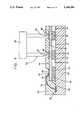
- a semiconductor chip 20may have a generally planar front face 22 (the face visible in FIG. 1) having a central region 24 adjacent the geometric center of the face and a peripheral region 26 adjacent the edges 28 bounding face 22.
- the front or contact-bearing face 22 of the chipis regarded as defining the top of the chip.
- the downward directionis the opposite direction.
- such termsshould be understood as based on this convention, and should not be understood as implying any particular directions with respect to the ordinary gravitational frame of reference.
- the chipalso has a plurality of peripheral contacts 30 arranged in rows 32, there being one such row adjacent each edge 28 of the chip.
- the rows 32do not intersect one another but instead terminate at appreciable distances from the corners of the chip so that the corners 34 are devoid of peripheral contacts 30.
- the central region 24 of the chip front surface 22is also devoid of contacts.
- the contacts 30 in each row 32are spaced at very close intervals typically about 100 to about 250 micrometers center to center. This center to center spacing is adequate for wire bonding or tape automated bonding.
- This chip configurationis typical of high I/O count chips originally intended for use with wire bonding or tape automated bonding systems.
- Interposer 36includes a flexible top layer 38 (FIG. 3) formed by a thin sheet of material having a relatively high elastic modulus and a compliant bottom layer 40 formed from a material having a relatively low elastic modulus.
- the high-modulus material of top layer 38may be a polymer such as a polyimide or other thermoset polymer, a fluoropolymer or a thermoplastic polymer.
- the compliant, low-modulus material of bottom layer 40may be an elastomer. Desirably, the low-modulus material has elastic properties (including modulus of elasticity) comparable to those of soft rubber, about 20 to 70 Shore A durometer hardness.
- Interposer 36has a first or bottom surface 42 defined by bottom layer 40 and a second or top surface 44 defined by top layer 38.
- Bottom, compliant layer 40includes holes or voids 41 interspersed with masses 43 of the low-modulus material.
- Interposer 36has edges 46 bounding surfaces 42 and 44 and extending therebetween.
- the interposeralso has a plurality of central terminals 48 distributed over the second or top surface 44. Terminals 48 are disposed at substantially even spaces on surface 44 so that terminals 48 constitute a "area array".
- the dimensions of interposer 36 in the plane of top surface 44are smaller than the corresponding dimensions of chip 20 in the plane of front surface 22.
- the number of central terminals 48may be approximately equal to the number of peripheral contacts 30 on the semiconductor chip Nonetheless, the center-to-center linear distance between adjacent ones of 30 central terminals 48 is substantially greater than the center-to-center distance between adjacent peripheral contacts 30 on the chip, because the central contacts 48 are substantially evenly distributed rather than concentrated in only a few rows.
- Each central terminal 48is aligned with one of the masses 43 of low-modulus material in compliant layer 40, whereas the holes 41 in the compliant layer are out of alignment with the central terminals 48.
- the holesmay be aligned with terminals 48.
- the holesmay be continuous with one another whereas the masses of low-modulus material may be separate posts or pillars entirely surrounded by such continuous holes.
- each central terminal 48is connected with a partial lead 50 and a bonding terminal 52 which are formed integrally with the central terminal.
- Central terminals 48, partial leads 50 and bonding terminals 52may be formed from substantially any electrically conductive material, but preferably are formed from metallic material such as copper and copper alloys, noble metals and noble metal alloys. These components typically are fabricated on the top or second surface 44 of interposer 36 by conventional photolithographic end etching or deposition techniques.
- Bonding terminals 52are arranged in rows 54 adjacent the edges 46 of the interposer. As best seen in FIG. 2, there are four such rows 54 of bonding terminals, one adjacent each edge of the interposer.
- the interposer 36 with the preformed terminals 48, partial leads 50 and bonding terminals 52 thereonis positioned on chip 20 so that the first surface 42 of the interposer faces the front surface 22 of the chip, and so that the edges 46 of the interposer are disposed inwardly of the rows 32 of peripheral contacts 30 on the chip.
- Bonding terminals 52are electrically connected to contacts 30 on the chip by a conventional wire bonding operation. The arrangement of the bonding terminals 52 in rows parallel to and adjacent to the rows of peripheral contacts 30 on the chip substantially facilitates the wire bonding process.
- the fine, flexible bonding wires 56 applied in the wire bonding operationmerge with the bonding terminals 52 and partial leads 50 on the interposer to form composite leads extending from the peripheral contacts of the chip to the central terminals on the interposer.
- each such composite leadextends inwardly from one peripheral contact 30 to an associated central terminal 48 in the central way.
- Each such composite leadextends across the edge 46 of the interposer.
- a low elastic modulus dielectric encapsulantsuch as a silicone rubber or other castable elastomer 58 (FIG. 4) is applied over the interposer and chip and over bonding wires 56.
- the encapsulantis applied so as to leave holes 60 in alignment with each of the central terminals 48 on the interposer. This may be accomplished by applying the encapsulant 58 in a selective coating process such as silk screening or the like; by applying the encapsulant to cover the entire assembly but then etching the encapsulant to form the holes, or by using a selective curing process.
- encapsulant 58may be an encapsulant which is curable by ultraviolet or other radiant energy.
- Radiant energymay be supplied selectively so that the areas overlying terminals 48 remained uncured and so that the encapsulant can then be removed from these areas by a washing or etching operation. At this stage, the assembly is relatively rugged and can be handled readily. Thus, the wires 56 are fully protected by the encapsulant.
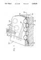
- the chip and all of the connections made within the assemblycan be tested by making temporary electrical connections to the central terminals 48.
- the central terminals 48are at substantial center-to-center distances, they may be readily contacted with probes such as the plural probe set 62 schematically illustrated in FIG. 4.
- each central terminal 48is displaceable towards and away from the front surface 22 of the chip 20.
- the bottom layercan be compressed by the tips 64 of the probe set 62. This greatly facilitates making good electrical contact between a plurality of probes and a plurality of central terminals at once, and hence greatly facilitates electrical testing of the chip and the other components of the assembly.
- compliant layer 40contributes to this action.
- Each mass 43 of low-modulus materialprovides backing and support for the aligned terminal 48.
- Holes 41provide space for such bulging.
- Compliant layer 40need only provide for sufficient downward movement of terminals 48 to accommodate tolerances in the components and test equipment by accommodating differences in vertical position between adjacent terminals and/or test probes. Typically, about 0.005 inch (0.125 mm) or less compliance is sufficient.
- complaint layer 40may be about 0.008 inch (0.2 mm) thick.
- test probe set 62is schematically illustrated as including only a few tips 64, the test probe set in fact may include a full compliment of tips 64, equal in number to the number of terminals 48, so that all of terminals 48 can be engaged simultaneously.
- the tips of probe set 62may be rigidly mounted to a common support 65. Therefore, the test probe set may be rugged, reliable and durable.
- the particular shape of tips 64is not critical. However, tips 64 may desirably be formed as small metallic spheres solder-bonded to support 65. Support 65 in turn may be a ceramic body with appropriate internal leads, similar to a conventional semiconductor substrate.
- test probe setmay make simultaneous connections with all terminals in the subassembly, and because the test probe set may have dimensions and configuration similar to a real substrate, the temporary electrical connection made using the test probe can provide a realistic test of the chip and interposer subassembly.
- the test probe setneed not involve long leads which may introduce unwanted inductance and/or capitance. Accordingly, the test probe set can be employed to test and operate the chip at full speed. Because the test probe set may be a simple, economical device, many such probe sets can be provided in a manufacturing plant, so that each chip can be tested for a prolonged period.
- the chip and interposer subassemblyis juxtaposed with a substrate 66 having electrical contact pads 68 thereon.
- the assemblyis placed on the substrate so that the central terminals 48 face toward the electrical contact pad 68 on the substrate, and so that each central terminal 48 is aligned with one contact pad 68.
- Masses of an electrically conductive bonding material 70such as a solder or an electrically conducted adhesive may be disposed between the central terminals and the contact pads of the substrate. These masses may then be caused to flow and to bond with the central terminals 48 and the contact pads 68 thereby forming mechanical and electrical connections between the central terminals and the contact pads.
- each contact pad 68 on the substratemay be a microminiature separable connector such as a socket, and a mating separable connector may be provided on each terminal 48.
- each terminal 48may incorporate a miniature pin adapted to engage such a socket. In this case, the pins would serve as the means for connecting terminals 48 to the contact pads of the substrate.
- each peripheral contact 30 on the chipis connected to one of the central terminals 48 on the interposer, and each such central terminal is connected to one of the contact pads 68 on the substrate, each peripheral contact 30 is connected to one of the contact pads 68 of the substrate.
- the substrate contact pad 68of course may be connected to other elements of an electrical circuit through conventional connections (not shown) incorporated in substrate 66.
- substrate 66may be a circuit board, circuit panel or hybrid circuit substrate incorporating various electronic elements in addition to chip 20.
- the interconnections between the chip and the substrateare accommodated within the area of the chip itself, i.e., within the area on the substrate occupied by chip 20.
- the assemblyis substantially resistant to thermal cycling.
- Each of the composite leads connecting one of the chip peripheral contacts and one of the central terminals 48 on the interposeris flexible.
- the partial leads 50 (FIG. 3) on the interposer surface itselfpreferably are flexible, and the fine bonding wires 56 are also flexible.
- the interposer itself, and particularly the top layer 38 and bottom compliant layer 40may be flexible.
- terminals 48 on the interposerthere can be substantial movement of terminals 48 on the interposer relative to contacts 30 on the chip in directions parallel to the chip front surface. Such movement can be accommodated without applying substantial forces to the junctions between the leads and the chip contacts.
- differential thermal expansion of chip 20 and substrate 66may cause appreciable displacement of contact pads 68 relative to peripheral contacts 30 on the chip.
- the central terminals 48 of the interposerare bonded to the contact pads by relatively stiff noncompliant conductive masses, the central terminals will tend to move with the contact pads.
- such movementis readily accommodated and does not result in substantial stresses at the bonds between the central terminals and contact pads.
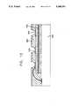
- the assembly shown in FIG. 6has an interposer 36' similar to the interposer discussed above with reference to FIGS. 1-5.
- the prefabricated leads 50' associated with terminals 48'have outer or contact portions 54' projecting outwardly beyond the edge 46' of the interposer.
- the prefabricated leads 50'are disposed on top layer 38' of the interposer, the prefabricated leads cross the edge 46' of the interposer at an appreciable height above the first or bottom surface 42' of the interposer.
- the projection, outer portions 54'are curved downwardly, toward the first surface 42' of the interposer. This curvature desirably is provided during fabrication of the interposer and leads, before the interposer is assembled to the chip.
- the interposer 36'with the leads 50' and terminals 48' already mounted thereon is placed onto chip 20' so that the outer portions 54' are in alignment with contacts 30' of the chip.
- the curvature of the leadsplaces the outer or contact portions 54' in close proximity to chip contacts 30'
- a tool 55is then applied to the outer portions 54' so as to force the outer portions thus forcing leads 54' into engagement with the chip contacts 30' so as to bond the outer portions 54 of leads 50' directly to the chip contacts.
- pressureis applied through tool 55 along with heat and/or ultrasonic energy.
- This stage of the processmay employ conventional thermal compression or ultrasonic bonding techniques commonly used to bond inner leads in a tape automated bonding or "TAB" operation.
- the terminals 48' and leads 50' used in this structurecan be fabricated by photolithigraphic techniques.
- the interposermay initially be fabricated with a solid sheet of copper or other metal covering the second surface 44' and extending beyond edges 46'. These portions of the metal sheet extending beyond the edges of the interposer may be embossed to impact a downward curvature
- the surface of the metallic layer facing upwardly away from the interposer(facing toward the top of the drawing in FIG. 6) may be covered with a conventional photo resist pattern such that the photo resist covers the areas corresponding to the terminals 48' and leads 50'.
- the opposite surface of the sheetmay be covered with a further photo resist in the areas extending beyond the edges 46' of the interposer.
- the sheetmay then be exposed to an etching solution so as to remove those areas not covered by the photo resist on the top surface, i.e., to remove all areas of the metal sheet other than the terminals 48' and leads 50'.
- the photo resistmay be removed, leaving interposer with the terminals and leads thereon.
- the curvature imported to the metal sheet by embossingprovides the desired downward curvature in the outer portions 54' of the leads.
- the leadsmay be bent after etching, using a forming die.
- the dielectric interposer, or one of the generally planar dielectric layers constituting the interposermay be provided with features projecting out of the plane of the layers, such as bumps or elongated ridges.
- the leadsmay be formed by depositing metal or other conductive material so that it forms leads extending over the projecting features and then removing those portions of the dielectric layer or interposer constituting the projecting features, as by selectively etching the dielectric layer, leaving behind leads which are curved out of the plane.
- the step of depositing the conductive material to form the leadsmay be performed by selectively depositing the conductive material using conventional techniques, or by depositing conductive material and selectively etching or otherwise removing conductive material before etching the dielectric layer.
- the assembly shown in FIG. 7includes an interposer 136 incorporating a flexible top layer 138 similar to the top layer 38 of the interposer discussed above with reference to FIGS. 1-5.
- Terminals 148 and leads 150 with outboard portions 154are positioned on the first or bottom surface 142 of the interposer, so that the terminals 148 face towards the chip 120 when the interposer is in position on the chip.
- the interposermay also include a separate compliant underlayer 140 disposed between the top layer 138 chip front surface 122, and also disposed beneath terminals 148, i.e., between the terminals and the chip.
- Layer 140may be positioned on chip surface 122, before layer 138, with the leads and terminals thereon, is positioned on layer 140.
- Layer 140may incorporate adhesives at its top and bottom surfaces so as to bind layer 138 to the chip. Because layer 140 is soft, layer 138 will remain flexible even when wound to the chip through layer 140, and terminals 138 will still be movable with respect to contacts 130.
- layer 140may be formed from a partially cured elastomer such as a so-called "B-stage" silicone elastomer. After assembly of layer 138, this partially cured material may be more fully cured, as by heating it, which causes the elastomer to bond with layer 138 and with chip surface 122. The portions 154 of the leads 150 are bonded to the chip contacts 130 to connect the chip contacts 130 with terminals 148.
- a compliant, low elastic modulus encapsulant 158is applied around the periphery of the interposer so as to encapsulate chip contacts 130 and the outward extensions 154 of leads 150. However, the encapsulant does not cover the first surface 144 of interposer 136. The terminals and leads are thus entirely surrounded and protected by the interposer, encapsulant and the chip itself.
- interposer top layer 138is punctured by applying radiant energy from a radiant energy source 159 such as a laser in registration with terminals 148 to thereby form holes 160 in alignment with the terminals.
- the resulting subassemblycan be bonded to a substrate in the same manner as discussed above with reference to FIG. 5.
- Masses of a bonding materialsuch as solder may be positioned within holes 160 so as to contact terminals 148, and these masses may be bonded to contact pads on the substrate.
- Holes 160may be formed before the interposer is connected to the chip, and indeed may be formed before the terminals 148 are positioned on the interposer.
- Terminals 148 and the associated leadsmay be formed on the interposer top layer 138 in substantially the same way as the contacts and terminals discussed above with reference to FIG. 6.
- the terminals and leadscan be provided on layer 140.
- FIG. 8The assembly illustrated in FIG. 8 is similar to the assembly of FIG. 6. However, the outboard portions 254 of leads 250 have outward extensions 256 projecting outwardly beyond chip peripheral contacts 230. These outward extensions 256 are secured to a securement element 260.
- securement element 260is a bar or strip of a polymeric, electrically nonconductive material. Although only one securement element 260 is visible in FIG. 8, it should be clearly appreciated that a similar securement element 260 is provided at each edge of the interposer, so that one such securement element extends generally parallel to each row of peripheral contacts 230, each said securement element lying outboard of the chip peripheral contacts.
- the securement elementserves to reinforce and support the outboard portions 254 of leads 250, and to prevent bending of the leads in undesired directions parallel to the surfaces of the interposer and chip.
- Securement element 260may be formed as part of a common sheet with the top layer 238 of interposer 236.
- the assembly shown in FIGS. 9, 10 and 15includes an interposer 336 and securement elements 361 similar to the interposer and securement elements discussed above with reference to FIG. 8. However, the central terminals 348 and peripheral contact leads 350 associated with interposer 336 are disposed on the first or chip-facing surface 342 of the interposer top layer 338. As best seen in FIG. 10, the securement elements 361 are connected to interposer 336 by bridge elements 363.
- the bridge elementsare disposed at spaced-apart locations around the periphery of the interposer.
- the interposer, securement elements and bridge elementsare formed as an integral unit. All of these components may be portions of a unitary sheet of dielectric material.
- the interposer 336, bridge elements 363 and securement elements 361may all be formed as part of an elongated tape 381,(FIG. 10) which may include several interposers 336, each with its associated securement elements and bridge elements.
- the tapemay also include waste or trim areas 383. During the various assembly and handling operations, the interposers and chips may be advanced through the process by advancing the tape.
- Bridge elements 363are disposed at the corners of the interposer.
- the chip 320 used in this assemblyincludes four rows 332 of peripheral contacts 330, the rows forming a generally rectangular pattern. However, the rows of peripheral contacts stop short of the corners of this rectangular pattern, so that the corner regions of the pattern are substantially devoid of contacts 330. Bridge elements 363 overlie these corner regions, and hence do not cover any of the contacts 330.
- Each securement element 361includes a top layer 301 (FIG. 9).
- Each securement elementhas an inboard edge 365 extending generally parallel to an edge 346 of interposer so that these parallel edges define an elongated slot 367 between the securement element and the interposer. Slots 367 are aligned with the rows 332 of chip peripheral contacts 330.
- the peripheral contact leads 350extend across slots 367, the outward extensions 354 of these leads being attached to the securement elements 361, so that each peripheral contact lead 350 is supported both by the interposer and by the securement element.
- Each securement element 361has a single row of outside terminals 372 extending generally parallel to the adjacent slot 367.
- Outside terminals 372are disposed on the first or chip-facing surface 369 of the top layers 301 securement element 361.
- Outside terminal leads 374(FIG. 9) extend inwardly from outside terminals 372 across slots 367.
- Each such outside terminal leadhas an inboard end 376 secured to the interposer 336.
- the outside terminal leads 372 and peripheral contact leads 350extend across slot 367. These leads are interspersed with one another along the length of each slot 367.
- Holes 360are provided in the interposer and in each securement element top layer in alignment with the central terminals 348 and outside terminals 372 so that the central terminals and outside terminals are accessible from the second surfaces of the interposer and securement elements, i.e., from the surface facing away from the chip.
- Interposer 336includes a compliant bottom layer 340, and each securement element 361 may include a compliant bottom layer 303 (FIG. 9). All of these compliant layers may be similar to the compliant layers discussed above, and may include holes (not shown) to increase their compliance.
- the compliant layers of the interposer and securement elementsmay be formed and assembled separately from these components, or may be incorporated in tape 381.
- the leads and terminalsmay be formed in place on the interposer and on the securement elements by an etching process similar to those described above.
- a copper or other metallic sheetmay be laminated to the dielectric sheet which will ultimately form the interposer top layer 338 and the securement element top layers 301, and then covered with a photoresist pattern and etched to form the various terminals and leads.
- Holes 360 and slots 367may be formed after the terminals and leads, by selectively applying radiant energy such as laser radiation to the sheet to selectively remove portions of the sheet. Alternatively, the slots and holes may be formed before the leads and terminals, as by etching or mechanically punching the dielectric sheet. The leads and terminals may then be formed by applying and selectively etching a metallic layer.
- Peripheral contact leads 350 and outside terminal leads 374are bent downwardly, toward the bottom of the interposer, within slots 367.
- the downward curvature of these leadsmay be formed by embossing the sheet used to fabricate these leads.
- a set of support elements 307is juxtaposed with chip 320 so that one such support element lies alongside each edge 309 of the chip.
- support elements 307may be provided as a unitary rectangular ring 311 which may closely surround the edges of the chip.
- Each support elementhas a top surface 313 arranged to lie substantially coplanar with the front or top surface 322 of the chip.
- chip 320 and support elements 307may be disposed on a planar carrier 315, and the thickness of the support elements may be substantially equal to the thickness of the chip.
- the interposer with the various terminals and leads thereonis positioned on the chip so that the slots, and hence the leads, are aligned with the peripheral contacts on the chip.
- Each securement element 361overlies one support element 307, and is at least partially supported by such element.
- a bonding toolis then advanced into each slot 367 and engaged with the peripheral contact leads 350 and with the outside terminal leads 372, so as to force each such lead into engagement with one of the peripheral contacts 330 on the chip. Heat-pressure and ultrasonic energy may be applied through the tool to promote bonding.
- the arrangement of the leads within the slotsgreatly facilitates the bonding operation.
- Bonding tool 355may be advanced into one of the slots 367 and moved along the length of the slot so as to bond all of the leads to all of the peripheral contacts 330 aligned with that slot. This process may be repeated for each slot 367. The tool may engage and bond many leads simultaneously.
- a low modulus dielectric encapsulant(not shown) is applied.
- the compliant layers 340 and 303may be formed by the encapsulant.
- the encapsulantmay be applied so as to penetrate between the interposer (not shown) and the chip to form compliant layer 340 between the interposer and the chip.
- the encapsulantmay also penetrate between securement elements 361 and support elements 307 to form compliant layers 303 in slots 367 to cover leads 374 and 350.
- the encapsulantmay be introduced under pressure in a liquid or flowable state and then cured.
- the interposer, chip and associated elementsmay be disposed in a mold during this process, and the mold may clamp the waste areas 383 of the sheet or tape (FIG. 10) so as to limit the flow of the encapsulant.
- the encapsulantmay be injected under pressure using standard injection molding technique.
- the assembly illustrated in FIGS. 9 and 10may be separated from the tape and mounted to a substrate in substantially the same way as the assemblies discussed above.
- both the outside terminals 372 and the central terminals 348may be bonded to contact pads on the substrate.
- the assembly illustrated in FIGS. 9 and 10provides good reinforcement of the leads during manufacture. Also, the outside terminals provide increased connection capacity. Although the securement elements and outside terminals extend outwardly beyond the peripheral contacts on the chip, this outward extension or "fan-out" is minimal. Preferably, the assembly with securement elements and outside terminals occupies an area in the plane parallel to the chip surface no more than about 1.5 times, and desirably no more than about 1.2 times, the area occupied by the chip itself.
- an interposer 436according to a further embodiment of the invention is provided with securement elements 461, slots 467 and outside terminals 472 similar to the corresponding components discussed above with reference to FIGS. 9 and 10.
- Outside terminals 472are disposed on the second surface of each securement element, i.e., on the surface directed away from the semiconductor chip 420.
- Interposer 436also has central terminals 448 on the second surface of the interposer. Each central terminal 448 is connected to a partial lead 450 and bonding terminal 452.
- each outside terminal 472is connected to a similar partial lead 475 and bonding terminal 477.
- the bonding terminalsare connected to the peripheral contacts 430 on chip 420 by a wire-bonding operation similar to that discussed above with reference to FIGS. 1-5.
- disposition of the bonding terminals in rowsfacilitates the wire-bonding operation.
- Chip 420also has central contacts 431 disposed in the central region of the chip front surface.
- Interposer 436has a hole 480 encompassing these central contacts.
- Some of the bonding terminals 452 associated with certain central terminals 448are disposed adjacent the edges of hole 480. These bonding terminals are connected by wire bonds to the central contacts 431 of the chip, so that the central contacts as well as the peripheral contacts 430 will be connected to the substrate through the central terminals 448 of the interposer.
- assemblies according to the inventionmay include additional elements for mechanical and electrical protection.
- a thin electrically conductive layersuch as a metallic layer 502 may be incorporated in the interposer to electrically isolate the central terminals 548 from the chip 520.
- a conductive layermust be separated from terminals 548 by a dielectric layer 538.
- a rigid cover layer 504may be provided to further protect the assembly during manufacturing operations.
- the interposeritself may include multiple layers of central terminals and leads separated from one another by intermediate dielectric layers. Such an arrangement allows the leads on the interposer to cross over one another without contacting one another, and allows for more leads and/or wider leads in a given area.
- the topmost layers of such a multilayer interposermay have holes aligned with the central terminals of the lower layers, to provide access to these lower-layer terminals and permit connection to a substrate.
- a semiconductor chip assemblyincludes a chip 620 having a generally planar front surface 622, a generally planar rear surface 623 extending substantially parallel to front surface 622 and edges 628 extending between these surfaces.
- the chiphas peripheral contacts 630 arranged in rows adjacent the edges of the chip.
- An interposer 636overlies the central region of the chip front surface. Interposer 636 has central terminals 648. These terminals are connected to the peripheral contacts 630 of the chip by leads 650. Leads 650 have outer extensions 654 extending outwardly beyond the peripheral contacts 630 and beyond the edges 628 of the chip.
- a sheetlike backing element 660abuts the rear face 623 of chip 620, so that the chip is sandwiched between backing element 660 and interposer 636.
- Backing element 660has a top surface 662 facing the chip and a bottom surface 664 facing away from the chip. The backing element extends outwardly beyond the edges 628 of the chip.
- Backing element 660has outside terminals 666 disposed outboard of the chip edges 628 on backing element top surface 662.
- the outward extensions 654 of the leads from interposer 636are connected to outside terminals 666, and hence the outward extensions are secured to the backing element.
- Outside terminals 666are electrically connected to inside terminals 668 disposed on the bottom surface 664 of the backing element.
- Inside terminals 668are disposed in the central region of the backing element, in alignment with the chip 620 and interposer 636.
- the pattern of inside terminals 668 on the backing elementdesirably corresponds to the pattern of central terminals 648 on the interposer 636.
- a plurality of these chip assembliescan be combined to form a larger, multi-chip circuit assembly.
- the chip assembliesare stacked one atop the other, with the backing element 660 of each chip assembly overlying the interposer 636 of the next lower chip assembly.
- the inside terminals 668 on the backing element of each chip assemblyare aligned with the central terminals 648 on the interposer of the immediately subjacent (next lower) chip assembly.
- These aligned terminalsare mechanically and electrically connected to one another, as by masses of electrically conductive bonding material 670 such as solder or electrically conductive adhesives.
- the leads and contacts of the various chip assembliesare electrically connected to one another, thereby connecting the chips to one another.
- the circuit assembly according to this aspect of the inventionmay be connected to a larger substrate by bonding the central terminals 648 on the interposer of the topmost chip assembly to a substrate, or by bonding the inside terminals 668 on the bottom chip assembly to a substrate, or both.
- Circuit assemblies according to this aspect of the present inventionare particularly useful for accommodating large numbers of chips in a small area. These assemblies are especially useful with memory chips such as random access memory chips.
- memory chipssuch as random access memory chips.
- plural memory chipscan be provided with parallel connections to a data bus and stacked in essentially the same circuit board area as ordinarily occupied by a single chip.
- the structureincludes an interposer 736 and securement elements 761 defining slots 767 therebetween, only one such securement element and slot being visible in FIG. 16.
- the outside terminal leads and peripheral leadsinclude portions 754 extending across the slots. Each such lead portion extends into the slot from above the compliant layer 703 of the associated securement element and above the compliant layer 740 of the interposer. In the condition illustrated in FIG. 16, before bonding of lead portions 754 to terminals 730 of the chip, these lead portions are substantially planar. That is, they extend substantially in a plane parallel to the plane of interposer 736 and hence parallel to the plane of chip front surface 722 when the interposer overlies the chip.
- each such leadis curved in this horizontal plane, in the direction of elongation of the slot.
- each such leadincludes end portion 780 and 782 at the edges of the slot, adjacent securement element 761 and interposer 736 respectively.
- Each lead portion 754further includes a middle portion 784 adjacent the center of the slot and overlying one of the peripheral contacts 730 on chip 720.
- Each such middle portion 784is offset from the imaginary axis connecting ends 780 and 782. As shown in FIG. 16, the offset is in the direction of elongation of slot 767.
- a tool 786is advanced into slot 767 to bond lead portion 754 to chip peripheral contact 730.
- the toolengages the middle portion 784 of each lead portion, and forces the middle portion downwardly into engagement with chip contact 730. Because the middle portion is offset from the axis connecting ends 780 and 782, this downward motion of the middle portion can be accommodated by a controlled twisting motion of the ends.
- the middle portion 784may also bend downwardly to some degree. This structure provides a controlled downward motion of middle portion 784. As each lead portion 754 is retained at ends 780 and 782 during this operation, the portions will remain in the desired positions and hence will be properly aligned with chip contact 730. As all of the middle portions 784 are offset in the same direction, the offsets in the lead portions do not appreciably increase the required spacings between lead portions 754 along the length of slot 767. Moreover, these offsets, lying in the plane of the interposer, can be formed without any separate embossing or bending operation, in the same etching operation used to form the leads.
- the bonding toolmay engage and bond the middle portions of several leads simultaneously.
- the bridge elements 363(FIG. 10) connecting an interposer with the associated securement elements need not be disposed at the corners of a chip.
- the interposerneed not overlie the entire front or top surface of the chip but may instead overlie only a portion of the chip front surface.
Landscapes
- Engineering & Computer Science (AREA)
- Microelectronics & Electronic Packaging (AREA)
- Power Engineering (AREA)
- Computer Hardware Design (AREA)
- Physics & Mathematics (AREA)
- Condensed Matter Physics & Semiconductors (AREA)
- General Physics & Mathematics (AREA)
- Manufacturing & Machinery (AREA)
- Geometry (AREA)
- Wire Bonding (AREA)
- Testing Of Individual Semiconductor Devices (AREA)
- Die Bonding (AREA)
- Internal Circuitry In Semiconductor Integrated Circuit Devices (AREA)
- Testing Or Measuring Of Semiconductors Or The Like (AREA)
- Measuring Leads Or Probes (AREA)
- Thermistors And Varistors (AREA)
Abstract
Description
This application is a continuation-in-part of U.S. patent application Ser. No. 07/586,758, filed Sept. 24, 1990, the disclosure of which is hereby incorporated by reference herein.
The present invention relates to the art of electronic packaging, and more specifically to assemblies incorporating semiconductor chips and to methods of making such assemblies.
Modern electronic devices utilize semiconductor chips, commonly referred to as "integrated circuits" which incorporate numerous electronic elements. These chips are mounted on substrates which physically support the chips and electrically interconnect each chip with other elements of the circuit. The substrate may be a part of a discrete chip package used to hold a single chip and equipped with terminals for interconnection to external circuit elements. Such substrates may be secured to an external circuit board or chassis. Alternatively, in a so-called "hybrid circuit" one or more chips are mounted directly to a substrate forming a circuit panel arranged to interconnect the chips and the other circuit elements mounted to the substrate. In either case, the chip must be securely held on the substrate and must be provided with reliable electrical interconnection to the substrate. The interconnection between the chip itself and its supporting substrate is commonly referred to as "first level" assembly or chip interconnection, as distinguished from the interconnection between the substrate and the larger elements of the circuit, commonly referred to as a "second level" interconnection.
The structures utilized to provide the first level connection between the chip and the substrate must accommodate all of the required electrical interconnections to the chip. The number of connections to external circuit elements, commonly referred to as "input-output" or "I/O" connections, is determined by the structure and function of the chip. Advanced chips capable of performing numerous functions may require substantial numbers of I/O connections.
The size of the chip and substrate assembly is a major concern. The size of each such assembly influences the size of the overall electronic device. Moreover, the size of each assembly controls the required distance between each chip and other chips, or between each chip or other elements of the circuit. Delays in transmission of electrical signals between chips are directly related to these distances. These delays limit the speed of operation of the device. For example, in a computer where a central processing unit operates cyclically, signals must be interchanged between the central processing unit chip and other chips during each cycle. The transmission delays inherent in such interchanges often limit the cycling rate of the central processing chip. Thus, more compact interconnection assemblies, with smaller distances between chips and smaller signal transmission delays can permit faster operation of the central processing chip.
The first level interconnection structures connecting a chip to a substrate ordinarily are subject to substantial strain caused by thermal cycling as temperatures within the device change during operation. The electrical power dissipated within the chip tends to heat the chip and substrate, so that the temperatures of the chip and substrate rise each time the device is turned on and fall each time the device is turned off. As the chip and the substrate ordinarily are formed from different materials having different coefficients of thermal expansion, the chip and substrate ordinarily expand and contract by different amounts. This causes the electrical contacts on the chip to move relative to the electrical contact pads on the substrate as the temperature of the chip and substrate changes. This relative movement deforms the electrical interconnections between the chip and substrate and places them under mechanical stress. These stresses are applied repeatedly with repeated operation of the device, and can cause breakage of the electrical interconnections. Thermal cycling stresses may occur even where the chip and substrate are formed from like materials having similar coefficients of thermal expansion, because the temperature of the chip may increase more rapidly than the temperature of the substrate when power is first applied to the chip.
The cost of the chip and substrate assembly is also a major concern. All these concerns, taken together, present a formidable engineering challenge. Various attempts have been made heretofore to provide primary interconnection structures and methods to meet these concerns, but none of these is truly satisfactory in every respect. At present, the most widely utilized primary interconnection methods are wire bonding, tape automated bonding or "TAB" and flip-chip bonding.
In wire bonding, the substrate has a top surface with a plurality of electrically conductive contact pads or lands disposed in a ring-like pattern, The chip is secured to the top surface of the substrate at the center of the ring-like pattern, so that the chip is surrounded by the contact pads on the substrate. The chip is mounted in a face-up disposition, with the back surface of the chip confronting the top surface of the substrate and with the front surface of the chip facing upwardly, away from the substrate, so that electrical contacts on the front surface are exposed. Fine wires are connected between the contacts on the front face of the chip and the contact pads on the top surface of the substrate. These wires extend outwardly from the chip to the surrounding contact pads on the substrate.
Wire bonding ordinarily can only be employed with contacts at the periphery of the chip. It is difficult or impossible to make connections with contacts at the center of the front surface of the chip using the wire bonding approach. Also, the contacts on the chip must be spaced at least about 100 micrometers apart from one another. These considerations limit the wire bonding approach to chips having relatively few I/O connections, typically less than about 250 connections per chip. Moreover, the area of the substrate occupied by the chip, the wires and the contact pads of the substrate is substantially greater than the surface area of the chip itself.
In tape automated bonding, a polymer tape is provided with thin layers of metallic material forming conductors on a first surface of the tape. These conductors are arranged generally in a ring-like pattern and extend generally radially, towards and away from the center of the ring-like pattern. The chip is placed on the tape in a face down arrangement, with contacts on the front surface of the chip confronting the conductors on the first surface of the tape. The contacts on the chip are bonded to the conductors on the tape. Ordinarily, numerous patterns of conductors are arranged along the length of the tape and one chip is bonded to each of these individual patterns, so that the chips, once bonded to the tape, can be advanced through successive work stations by advancing the tape. After each chip is bonded to the metallic conductors constituting one pattern, the chip and the immediately adjacent portions of the pattern are encapsulated and the outermost portions of the metallic conductors are secured to additional leads and to the ultimate substrate. Tape automated bonding can provide the assembly with good resistance to thermal stresses, because the thin metallic leads on the tape surface are quite flexible, and will bend readily upon expansion of the chip without imposing significant stresses at the juncture between the lead and the contact on the chip. However, because the leads utilized in tape automated bonding extend outwardly in a radial, "fan out" pattern from the chip, the assembly is much larger than the chip itself. Also, the leads ordinarily are connected only to contacts at the periphery of the chip. This limits tape automated bonding to chips having relatively low numbers of contacts.
In flip-chip bonding, contacts on the front surface of the chip are provided with bumps of solder. The substrate has contact pads arranged in an array corresponding to the array of contacts on the chip. The chip, with the solder bumps, is inverted so that its front surface faces toward the top surface of the substrate, with each contact and solder bump on the chip being positioned on the appropriate contact pad of the substrate. The assembly is then heated so as to liquify the solder and bond each contact on the chip to the confronting contact pad of the substrate. Because the flip-chip arrangement does not require leads arranged in a fan-out pattern, it provides a compact assembly. The area of the substrate occupied by the contact pads is approximately the same size as the chip itself. Moreover, the flip-chip bonding approach is not limited to contacts on the periphery of the chip. Rather, the contacts on the chip may be arranged in a so-called "area array" covering substantially the entire front face of the chip. Flip-chip bonding therefore is well suited to use with chips having large numbers of I/O contacts. However, assemblies made by flip-chip bonding are quite susceptible to thermal stresses. The solder interconnections are relatively inflexible, and may be subjected to very high stress upon differential expansion of the chip and substrate. These difficulties are particularly pronounced with relatively large chips. Moreover, it is difficult to test and operate or "burn-in" chips having an area array of contacts before attaching the chip to the substrate. Additionally, flip-chip bonding ordinarily requires that the contacts on the chip be arranged in an area array to provide adequate spacing for the solder bumps. Flip-chip bonding normally cannot be applied to chips originally designed for wire bonding or tape automated bonding, and having rows of closely spaced contacts on the periphery of the chip.
Our own prior U.S. patent application Ser. No. 07/586,758 discloses improvements in semiconductor chip assemblies and methods of making the same. As more fully set forth in the '758 application, a semiconductor chip can be connected to a substrate using a sheet-like, and preferably flexible, interposer. The interposer overlies the top, contact-bearing surface of the chip. A first surface of the interposer faces towards the chip whereas a second surface faces away from the chip. Electrical terminals are provided on the second surface of the interposer, and the interposer is also provided with apertures extending through it. Flexible leads extend through these apertures between contacts on the chip and the terminals on the second surface of the interposer. The terminals can be bonded to a substrate. Because the terminals are movable relative to the contacts on the chip, the arrangements described in the '758 application provide excellent resistance to thermal cycling. The interposer disclosed in the '758 application may include a soft, compliant layer disposed between the terminals and the chip. Because the terminals can be disposed in the area of the interposer overlying the contact pattern area of the chip, the structures described in the '758 application provide extraordinarily compact assemblies, substantially as compact as those achieved by flip-chip bonding. The invention described in the '758 application can be used with substantially any chip configuration, including so-called peripheral contact chips having contacts arranged in rows adjacent the periphery of the chip, as well as so-called area array chips having contacts disposed in an array substantially covering the entire face of the chip.
However, still further improvements would be desirable. In particular, there are needs for still further improvements in mountings to accommodate chips having peripheral contacts. Most conventional chips such as random access memories and the more common microprocessors are commonly manufactured with peripheral contact arrangements.
The present invention addresses these needs.
One aspect of the present invention provides semiconductor chip assemblies. A chip assembly according to this aspect of the present invention preferably incorporates a chip having a front or top surface including a central region and a peripheral region surrounding the central region, the chip having a plurality of peripheral contacts disposed in the peripheral region of the front surface. The assembly preferably further includes a sheet-like dielectric interposer overlying the central region of the chip front surface. The interposer has a first surface facing downwardly toward the chip and a second surface facing upwardly, away from the chip. The interposer also has edges disposed inwardly of the peripheral contacts. For example, the interposer may overly only the central portion of the chip front surface. A plurality of central terminals are disposed on the interposer and overly the central region of the chip front surface. The assembly preferably also includes a plurality of peripheral contact leads connecting at least some of the peripheral contacts on the chip with at least some of the central terminals on the interposer. Each such peripheral contact lead thus has a central terminal end overlying the interposer and connected to one of the central terminals and a contact end projecting outwardly beyond one of the edges of the interposer and connected to one of the peripheral contacts. Each peripheral contact lead extends inwardly from one of the peripheral contacts to one of the central terminals on the interposer. The peripheral contact leads and preferably the interposer as well are at least partially flexible so that the central terminals are movable with respect to peripheral contacts to accommodate movement caused by differential thermal expansion. Desirably, the peripheral contact leads include bent portions.
The peripheral contact leads and central terminals provide a "fan-in" arrangement in which the terminals on the interposer are disposed inside the region bounded by the peripheral contacts on the chip. Typically, the peripheral contacts on the chip are disposed in one or two rows along each edge of the chip, in a generally rectangular pattern, so that the contacts on the chip are close to one another. By contrast, the terminals on the interposer may be substantially evenly disposed over the second surface of the interposer. The central terminals may be disposed in a so-called "area array". Accordingly, the distance between adjacent terminals may be substantially greater than the distance between adjacent contacts on the chip. The distances between adjacent terminals on the interposer may be large enough to accommodate solder bonding and similar processes which require substantial distances between adjacent bonds. Such bonds may be accommodated in the previously unused area overlying the center of the chip. The peripheral contact leads may be connected to the peripheral contacts of the chip by a bonding method similar to those used with conventional "fan-out" leads, such as wire bonding or thermal compression bonding. The chip assembly may further include a substrate having electrically conductive contact pads, the chip and interposer being superposed on the substrate so that the second surface of the interposer faces toward the substrate and, preferably, so that the terminals on the interposer are aligned with the contact pads on the substrate. The interposer terminals and the substrate contact pads may be electrically connected and secured to one another, as by an electrically conductive material such as solder disposed therebetween. Assemblies according to preferred embodiments of this aspect of the invention provide both compactness and resistance to thermal stress.
Some or all of the peripheral contact leads may have outward extensions projecting outwardly beyond the peripheral contacts of the chip. The assembly may include securement means for holding these outward extensions. For example, one or more securement elements may be disposed outwardly of the peripheral contacts, and each such securement element may be physically connected to a plurality of the outward extensions on the peripheral contact leads. Each such securement element may be a generally planar strip of dielectric material having an inboard edge extending generally parallel to one of the edges of the interposer so that each pair of parallel edges define an elongated slot between each such securement element and the interposer, and each peripheral contact lead may extend across one of these slots. In this arrangement, the peripheral contacts of the chip may be disposed in alignment with the slots between the securement elements and the interposer. The securement element may be physically connected to the interposer, as by bridge elements extending between the securement elements and the interposer at spaced-apart locations around the periphery of the chip front surface. The securement elements, bridge elements and interposer may be formed integrally with one another as a single, sheet-like unit. The bridge elements may be disposed at the corners of a rectangular or other polygonal chip contact pattern. The securement elements provide physical reenforcement to the peripheral contact leads during the manufacturing operations and in service. Additional terminals, referred to herein as "outside" terminals, may be disposed on the securement elements, and may be connected to some of the peripheral contacts on the chip by outside terminal leads extending across the slots, the inboard ends of the outside terminal leads being secured to the interposer so that the slot and interposer cooperatively provide reinforcement to the outside terminal leads as well.
The interposer desirably includes a compliant layer of a material having a relatively low elastic modulus, such as an elastomeric material. This compliant layer is disposed beneath the central terminals, i.e., between the central terminals and the front surface of the chip. It permits slight downward movement of the central terminals towards the front face of the chip. As further explained below, this greatly facilitates temporary engagement of the central terminals by test equipment and hence facilitates testing and "burn-in" of the chip and interposer assembly before the same is mounted to a substrate. A further aspect of the present invention incorporates the realization that the compliance of such a compliant layer may be substantially enhanced by providing holes in the compliant layer, so that the compliant layer includes masses of compliant material interspersed with holes. Desirably, each such mass is aligned with one of the central terminals. This aspect of the present invention is not limited to assemblies incorporating the particular peripheral contact and central terminal arrangement mentioned above. It can be used in other arrangements incorporating a compliant layer disposed between terminals and a chip, such as the assemblies described in our U.S. patent application Ser. No. 07/586,758.
The semiconductor chip typically has a rear or bottom surface extending generally parallel to the front surface of the chip, and has edges extending between these front and rear surfaces at the outer periphery of the chip, outboard of the peripheral contacts. In a variant of the present invention, the securement means may include a backing element having a top surface overlying the rear surface of the chip, the backing element extending outwardly beyond at least some of the edges of the chip. At least some of the outboard extensions of the peripheral contact leads may extend beyond the edges of the chip and may be secured to the backing element. The backing element may support outside terminals outboard of the edges of the chip, and at least some of the outboard extensions of the peripheral contact leads may be connected to the outside terminals on the backing element. The backing element may have inside terminals disposed in a central region of the backing element aligned with the chip, and the central terminals may be electrically connected to the outside terminals of the backing element. In this arrangement, the chip is disposed between the backing element and the interposer, with the interposer on the front of the chip and the backing element on the back of the chip, both elements bearing terminals connected to the peripheral contacts of the chip.
A further aspect of the present invention provides a circuit assembly including a plurality of chip assemblies, each including an interposer and a backing element as discussed above. According to this aspect of the invention, the chip assemblies may be arranged in a stack, one on top of the other, such that each chip assembly other than the bottom-most chip assembly overlies another, immediately subjacent chip assembly. The bottom surface of the backing element in each such overlying chip assembly faces the second surface of the interposer of the immediate subjacent chip assembly. Most preferably, at least some of the inside terminals on the backing element of each such overlying chip assembly are connected to the central terminals on the interposer of the immediately subjacent chip assembly, so that the chips of the various chip assemblies are electrically connected to one another. Preferably, the inside terminals of the backing element of each chip assembly are aligned with the central terminals on the interposer of the immediately subjacent chip assembly. Preferably, the aligned inside and central terminals are connected to one another by masses of electrically conductive material such as solder disposed therebetween.
As discussed above, the chip assemblies, according to this aspect of the present invention, are particularly useful in the case of chips having peripheral contacts. The chip may also have a pattern of central contact disposed on the central region of the front surface. In this case, the interposer may have a hole aligned with the central contact pattern and inboard edges bounding the hole. The assembly may incorporate central contact leads extending from at least some of the central contacts on the chip to at least some of the central terminals on the interposer. In this case, the central contact leads extend outwardly in a "fan-out" pattern from the center of the chip towards the periphery of the chip, whereas the peripheral contact leads extend inwardly in a "fan-in" pattern from the periphery of the chip toward the center of the chip.
Further aspects of the present invention provide methods of making semiconductor assemblies. One method according to this aspect of the present invention includes the steps of providing a semiconductor chip having central and peripheral regions and peripheral contacts disposed in the peripheral region of the front surface. The method further includes the step of assembling a sheet-like dielectric interposer to the chip so that the interposer overlies the central region of the chip front surface, the outboard edges of the interposer being disposed inwardly of the peripheral contacts on the chip. When the dielectric interposer is disposed on the chip, a first surface of the interposer faces downwardly toward the chip and a second surface of the interposer faces upwardly away from the chip, and a plurality of central terminals on the interposer overly the central region of the chip front surface. The method further includes the step of connecting a plurality of peripheral contact leads between at least some of the peripheral contacts of the chip and at least some of the central terminals on the interposer, so that each such peripheral contact lead extends inwardly from one of the peripheral contacts on the chip to one of the central terminals on the interposer. The method may further include the step of assembling a substrate having a plurality of contact pads to be assembled interposer and chip and connecting each of the central terminals on the interposer to one of the contact pads on the substrate.
The interposer may have prefabricated leads mounted thereon and connected to the central terminals before the interposer is assembled to the chip. In this case, the prefabricated contact leads are positioned on the chip when the interposer is assembled to the chip. Such prefabricated contact leads may be electrically connected to the contacts of the chip by thermal compression bonding or similar processes. Alternatively, the peripheral contact leads may be formed after the interposer is applied to the chip, as in a wire-bonding step in which a fine wire is dispensed and formed into a lead connecting the contact and terminal. Preferably, securement elements are provided as discussed above with reference to the chip assembly, and the securement elements are connected to the interposer before the interposer is placed on the chip. In this case, the securement elements may support the prefabricated leads during the step of placing the interposer on the chip. The fabrication method according to this aspect of the present invention desirably further includes the step of connecting the terminals on the interposer to contact pads on a substrate. Also, the method according to this aspect of the present invention, desirably includes the step of applying an encapsulant to cover at least the peripheral contacts on the chip. Preferably, the encapsulant is applied so that it does not cover the central terminals on the interposer.
Assembly methods according to this aspect of the invention can provide simple and economical assembly of the chips to the substrates.
Still further aspects of the present invention provide prefabricated interposers having features as discussed above in connection with the assemblies and assembly methods. The interposers, with terminals and, preferably, prefabricated leads can be made and sold as separate articles of manufacture. These interposers can be employed in assembly methods and assemblies, as discussed above.
These and other objects, features and advantages of the present invention will be more readily apparent from the detailed description of the preferred embodiment set forth below, taken in conjunction with the accompanying drawings.
FIG. 1 is a diagrammatic plane view of a semiconductor chip incorporated in one embodiment of the present invention.
FIG. 2 is a view similar to FIG. 1 but showing the chip in conjunction with additional components.
FIG. 3 is a fragmentary, partially sectional perspective view on an enlarged scale depicting portions of the components illustrated in FIG. 2.
FIG. 4 is a fragmentary, diagrammatic sectional view depicting the components shown in FIG. 3 together with additional components and process equipment.
FIG. 5 is a view similar to FIG. 4, depicting the same components in conjunction with additional components.
FIG. 6 is a fragmentary, diagrammatic sectional view depicting an assembly operation according to a further embodiment of the invention.
FIG. 7 is a fragmentary, diagrammatic perspective view depicting a manufacturing operation and components according to still another embodiment of the invention.
FIG. 8 is a fragmentary diagrammatic perspective view depicting an assembly according to yet another embodiment of the invention.
FIG. 9 is a fragmentary, partially sectional diagrammatic perspective view depicting an assembly according to a further embodiment of the invention.
FIG. 10 is a diagrammatic plane view depicting the assembly of FIG. 9.
FIG. 11 is a diagrammatic plane view depicting an assembly according to yet another embodiment of the invention.
FIG. 12 is a fragmentary diagrammatic sectional view similar to FIG. 4 but depicting an assembly according to a further embodiment of the invention.
FIG. 13 is a diagrammatic perspective view depicting an assembly according to yet another embodiment of the invention.
FIG. 14 is a diagrammatic elevational view depicting an assembly in accordance with a further embodiment.
FIG. 15 is a fragmentary plan view depicting certain components used in the assembly according to FIGS. 9 and 10.
FIG. 16 is a fragmentary perspective view similar to FIG. 10 but depicting portions of any assembly in accordance with a further embodiment of the invention
As shown in FIG. 1, asemiconductor chip 20 may have a generally planar front face 22 (the face visible in FIG. 1) having acentral region 24 adjacent the geometric center of the face and aperipheral region 26 adjacent theedges 28 boundingface 22. The front or contact-bearingface 22 of the chip is regarded as defining the top of the chip. Thus, in specifying direction pointing out offront face 22, and away from the chip, i.e., the direction pointing out of the plane of the drawing towards the viewer in FIG. 1. The downward direction is the opposite direction. As used in the present disclosure with respect to a semiconductor chip assembly, such terms should be understood as based on this convention, and should not be understood as implying any particular directions with respect to the ordinary gravitational frame of reference. The chip also has a plurality ofperipheral contacts 30 arranged inrows 32, there being one such row adjacent eachedge 28 of the chip. Therows 32 do not intersect one another but instead terminate at appreciable distances from the corners of the chip so that thecorners 34 are devoid ofperipheral contacts 30. Thecentral region 24 of thechip front surface 22 is also devoid of contacts. Thecontacts 30 in eachrow 32 are spaced at very close intervals typically about 100 to about 250 micrometers center to center. This center to center spacing is adequate for wire bonding or tape automated bonding. This chip configuration is typical of high I/O count chips originally intended for use with wire bonding or tape automated bonding systems.
In an assembly method according to one embodiment of the invention, a sheet-likedielectric interposer 36 is assembled tochip 20.Interposer 36 includes a flexible top layer 38 (FIG. 3) formed by a thin sheet of material having a relatively high elastic modulus and a compliantbottom layer 40 formed from a material having a relatively low elastic modulus. The high-modulus material oftop layer 38 may be a polymer such as a polyimide or other thermoset polymer, a fluoropolymer or a thermoplastic polymer. The compliant, low-modulus material ofbottom layer 40 may be an elastomer. Desirably, the low-modulus material has elastic properties (including modulus of elasticity) comparable to those of soft rubber, about 20 to 70 Shore A durometer hardness.Interposer 36 has a first orbottom surface 42 defined bybottom layer 40 and a second ortop surface 44 defined bytop layer 38. Bottom,compliant layer 40 includes holes or voids 41 interspersed withmasses 43 of the low-modulus material.
As best seen in FIG. 3, eachcentral terminal 48 is connected with apartial lead 50 and abonding terminal 52 which are formed integrally with the central terminal.Central terminals 48, partial leads 50 andbonding terminals 52 may be formed from substantially any electrically conductive material, but preferably are formed from metallic material such as copper and copper alloys, noble metals and noble metal alloys. These components typically are fabricated on the top orsecond surface 44 ofinterposer 36 by conventional photolithographic end etching or deposition techniques.Bonding terminals 52 are arranged inrows 54 adjacent theedges 46 of the interposer. As best seen in FIG. 2, there are foursuch rows 54 of bonding terminals, one adjacent each edge of the interposer.
In the assembly method according to this embodiment of the invention, theinterposer 36 with the preformedterminals 48, partial leads 50 andbonding terminals 52 thereon is positioned onchip 20 so that thefirst surface 42 of the interposer faces thefront surface 22 of the chip, and so that theedges 46 of the interposer are disposed inwardly of therows 32 ofperipheral contacts 30 on the chip.Bonding terminals 52 are electrically connected tocontacts 30 on the chip by a conventional wire bonding operation. The arrangement of thebonding terminals 52 in rows parallel to and adjacent to the rows ofperipheral contacts 30 on the chip substantially facilitates the wire bonding process. The fine,flexible bonding wires 56 applied in the wire bonding operation merge with thebonding terminals 52 andpartial leads 50 on the interposer to form composite leads extending from the peripheral contacts of the chip to the central terminals on the interposer. As best appreciated with reference to FIG. 3, each such composite lead extends inwardly from oneperipheral contact 30 to an associatedcentral terminal 48 in the central way. Each such composite lead extends across theedge 46 of the interposer.
In the next stage of the process, a low elastic modulus dielectric encapsulant such as a silicone rubber or other castable elastomer 58 (FIG. 4) is applied over the interposer and chip and overbonding wires 56. The encapsulant is applied so as to leaveholes 60 in alignment with each of thecentral terminals 48 on the interposer. This may be accomplished by applying theencapsulant 58 in a selective coating process such as silk screening or the like; by applying the encapsulant to cover the entire assembly but then etching the encapsulant to form the holes, or by using a selective curing process. Thus, encapsulant 58 may be an encapsulant which is curable by ultraviolet or other radiant energy. Radiant energy may be supplied selectively so that theareas overlying terminals 48 remained uncured and so that the encapsulant can then be removed from these areas by a washing or etching operation. At this stage, the assembly is relatively rugged and can be handled readily. Thus, thewires 56 are fully protected by the encapsulant.
Either before or after theencapsulant 58 is applied, the chip and all of the connections made within the assembly can be tested by making temporary electrical connections to thecentral terminals 48. Because thecentral terminals 48 are at substantial center-to-center distances, they may be readily contacted with probes such as the plural probe set 62 schematically illustrated in FIG. 4. Moreover, because thebottom layer 40 of the interposer is compliant, eachcentral terminal 48 is displaceable towards and away from thefront surface 22 of thechip 20. Thus, the bottom layer can be compressed by thetips 64 of the probe set 62. This greatly facilitates making good electrical contact between a plurality of probes and a plurality of central terminals at once, and hence greatly facilitates electrical testing of the chip and the other components of the assembly. The configuration ofcompliant layer 40 contributes to this action. Eachmass 43 of low-modulus material provides backing and support for the alignedterminal 48. As thetips 64 of the test probe set 62 engage the terminals, each mass 43 is compressed in the vertical direction and therefore tends to bulge in horizontal directions, parallel to the plane of the chip.Holes 41 provide space for such bulging.Compliant layer 40 need only provide for sufficient downward movement ofterminals 48 to accommodate tolerances in the components and test equipment by accommodating differences in vertical position between adjacent terminals and/or test probes. Typically, about 0.005 inch (0.125 mm) or less compliance is sufficient. For example,complaint layer 40 may be about 0.008 inch (0.2 mm) thick.
Although test probe set 62 is schematically illustrated as including only afew tips 64, the test probe set in fact may include a full compliment oftips 64, equal in number to the number ofterminals 48, so that all ofterminals 48 can be engaged simultaneously. The tips of probe set 62 may be rigidly mounted to acommon support 65. Therefore, the test probe set may be rugged, reliable and durable. The particular shape oftips 64 is not critical. However,tips 64 may desirably be formed as small metallic spheres solder-bonded to support 65.Support 65 in turn may be a ceramic body with appropriate internal leads, similar to a conventional semiconductor substrate. Because the test probe set may make simultaneous connections with all terminals in the subassembly, and because the test probe set may have dimensions and configuration similar to a real substrate, the temporary electrical connection made using the test probe can provide a realistic test of the chip and interposer subassembly. In particular, the test probe set need not involve long leads which may introduce unwanted inductance and/or capitance. Accordingly, the test probe set can be employed to test and operate the chip at full speed. Because the test probe set may be a simple, economical device, many such probe sets can be provided in a manufacturing plant, so that each chip can be tested for a prolonged period.
In the next stage of the assembly operation after testing, the chip and interposer subassembly is juxtaposed with a substrate 66 havingelectrical contact pads 68 thereon. The assembly is placed on the substrate so that thecentral terminals 48 face toward theelectrical contact pad 68 on the substrate, and so that eachcentral terminal 48 is aligned with onecontact pad 68. Masses of an electricallyconductive bonding material 70 such as a solder or an electrically conducted adhesive may be disposed between the central terminals and the contact pads of the substrate. These masses may then be caused to flow and to bond with thecentral terminals 48 and thecontact pads 68 thereby forming mechanical and electrical connections between the central terminals and the contact pads. This stage of the process may utilize essentially the same techniques as are employed in surface mount technology for assembly of components on printed circuit boards. Because thecentral terminals 48 are disposed at substantial center-to-center distances, the standard surface mount techniques can be used without difficulty. For example, a high I/O count can be achieved with 20-25 mil (500-625 micrometer) center-to-center distances. In an alternate embodiment, eachcontact pad 68 on the substrate may be a microminiature separable connector such as a socket, and a mating separable connector may be provided on each terminal 48. For example, each terminal 48 may incorporate a miniature pin adapted to engage such a socket. In this case, the pins would serve as the means for connectingterminals 48 to the contact pads of the substrate.
Inasmuch as eachperipheral contact 30 on the chip is connected to one of thecentral terminals 48 on the interposer, and each such central terminal is connected to one of thecontact pads 68 on the substrate, eachperipheral contact 30 is connected to one of thecontact pads 68 of the substrate. Thesubstrate contact pad 68 of course may be connected to other elements of an electrical circuit through conventional connections (not shown) incorporated in substrate 66. For example, substrate 66 may be a circuit board, circuit panel or hybrid circuit substrate incorporating various electronic elements in addition tochip 20.
The interconnections between the chip and the substrate (betweenperipheral contacts 30 and contact pads 68) are accommodated within the area of the chip itself, i.e., within the area on the substrate occupied bychip 20. Thus, no space on the surface of the substrate is wasted by a conventional "fan-out" pattern of interconnections. Moreover, the assembly is substantially resistant to thermal cycling. Each of the composite leads connecting one of the chip peripheral contacts and one of thecentral terminals 48 on the interposer is flexible. Thus, the partial leads 50 (FIG. 3) on the interposer surface itself preferably are flexible, and thefine bonding wires 56 are also flexible. The interposer itself, and particularly thetop layer 38 and bottomcompliant layer 40 may be flexible. Accordingly, there can be substantial movement ofterminals 48 on the interposer relative tocontacts 30 on the chip in directions parallel to the chip front surface. Such movement can be accommodated without applying substantial forces to the junctions between the leads and the chip contacts. During use of the assembly, differential thermal expansion ofchip 20 and substrate 66 may cause appreciable displacement ofcontact pads 68 relative toperipheral contacts 30 on the chip. Inasmuch as thecentral terminals 48 of the interposer are bonded to the contact pads by relatively stiff noncompliant conductive masses, the central terminals will tend to move with the contact pads. However, such movement is readily accommodated and does not result in substantial stresses at the bonds between the central terminals and contact pads.
The assembly shown in FIG. 6 has an interposer 36' similar to the interposer discussed above with reference to FIGS. 1-5. However, the prefabricated leads 50' associated with terminals 48' have outer or contact portions 54' projecting outwardly beyond the edge 46' of the interposer. As prefabricated leads 50' are disposed on top layer 38' of the interposer, the prefabricated leads cross the edge 46' of the interposer at an appreciable height above the first or bottom surface 42' of the interposer. The projection, outer portions 54' are curved downwardly, toward the first surface 42' of the interposer. This curvature desirably is provided during fabrication of the interposer and leads, before the interposer is assembled to the chip. In the assembly operation, the interposer 36', with the leads 50' and terminals 48' already mounted thereon is placed onto chip 20' so that the outer portions 54' are in alignment with contacts 30' of the chip. The curvature of the leads places the outer or contact portions 54' in close proximity to chip contacts 30' Atool 55 is then applied to the outer portions 54' so as to force the outer portions thus forcing leads 54' into engagement with the chip contacts 30' so as to bond theouter portions 54 of leads 50' directly to the chip contacts. Typically, pressure is applied throughtool 55 along with heat and/or ultrasonic energy. This stage of the process may employ conventional thermal compression or ultrasonic bonding techniques commonly used to bond inner leads in a tape automated bonding or "TAB" operation. This bonding establishes a connection between each chip contact 50' and one of the terminals 48' on the interposer, without the need for any intermediate wire bonding operation. Once the contacts and terminals are connected in this manner, the resulting subassembly can be encapsulated and bonded to a substrate in substantially the same fashion as discussed above. A leads 50' are flexible, terminals 48' are movable with respect to contacts 30' to compensate for thermal expansion.
The terminals 48' and leads 50' used in this structure can be fabricated by photolithigraphic techniques. For example, the interposer may initially be fabricated with a solid sheet of copper or other metal covering the second surface 44' and extending beyond edges 46'. These portions of the metal sheet extending beyond the edges of the interposer may be embossed to impact a downward curvature The surface of the metallic layer facing upwardly away from the interposer (facing toward the top of the drawing in FIG. 6) may be covered with a conventional photo resist pattern such that the photo resist covers the areas corresponding to the terminals 48' and leads 50'. The opposite surface of the sheet may be covered with a further photo resist in the areas extending beyond the edges 46' of the interposer. The sheet may then be exposed to an etching solution so as to remove those areas not covered by the photo resist on the top surface, i.e., to remove all areas of the metal sheet other than the terminals 48' and leads 50'. The photo resist may be removed, leaving interposer with the terminals and leads thereon. The curvature imported to the metal sheet by embossing provides the desired downward curvature in the outer portions 54' of the leads. Alternatively, the leads may be bent after etching, using a forming die. In yet another lead-forming method, the dielectric interposer, or one of the generally planar dielectric layers constituting the interposer may be provided with features projecting out of the plane of the layers, such as bumps or elongated ridges. The leads may be formed by depositing metal or other conductive material so that it forms leads extending over the projecting features and then removing those portions of the dielectric layer or interposer constituting the projecting features, as by selectively etching the dielectric layer, leaving behind leads which are curved out of the plane. The step of depositing the conductive material to form the leads may be performed by selectively depositing the conductive material using conventional techniques, or by depositing conductive material and selectively etching or otherwise removing conductive material before etching the dielectric layer.
The assembly shown in FIG. 7 includes aninterposer 136 incorporating a flexibletop layer 138 similar to thetop layer 38 of the interposer discussed above with reference to FIGS. 1-5.Terminals 148 and leads 150 withoutboard portions 154 are positioned on the first orbottom surface 142 of the interposer, so that theterminals 148 face towards thechip 120 when the interposer is in position on the chip. The interposer may also include a separatecompliant underlayer 140 disposed between thetop layer 138 chipfront surface 122, and also disposed beneathterminals 148, i.e., between the terminals and the chip.Layer 140 may be positioned onchip surface 122, beforelayer 138, with the leads and terminals thereon, is positioned onlayer 140.Layer 140 may incorporate adhesives at its top and bottom surfaces so as to bindlayer 138 to the chip. Becauselayer 140 is soft,layer 138 will remain flexible even when wound to the chip throughlayer 140, andterminals 138 will still be movable with respect tocontacts 130. Alternatively,layer 140 may be formed from a partially cured elastomer such as a so-called "B-stage" silicone elastomer. After assembly oflayer 138, this partially cured material may be more fully cured, as by heating it, which causes the elastomer to bond withlayer 138 and withchip surface 122. Theportions 154 of theleads 150 are bonded to thechip contacts 130 to connect thechip contacts 130 withterminals 148. A compliant, lowelastic modulus encapsulant 158 is applied around the periphery of the interposer so as to encapsulatechip contacts 130 and theoutward extensions 154 ofleads 150. However, the encapsulant does not cover thefirst surface 144 ofinterposer 136. The terminals and leads are thus entirely surrounded and protected by the interposer, encapsulant and the chip itself. To provide access to theterminals 148 from the second surface of the interposer, interposertop layer 138 is punctured by applying radiant energy from aradiant energy source 159 such as a laser in registration withterminals 148 to thereby formholes 160 in alignment with the terminals. Once theholes 160 have been formed, the resulting subassembly can be bonded to a substrate in the same manner as discussed above with reference to FIG. 5. Masses of a bonding material such as solder may be positioned withinholes 160 so as to contactterminals 148, and these masses may be bonded to contact pads on the substrate.
The assembly illustrated in FIG. 8 is similar to the assembly of FIG. 6. However, theoutboard portions 254 ofleads 250 haveoutward extensions 256 projecting outwardly beyond chipperipheral contacts 230. Theseoutward extensions 256 are secured to asecurement element 260. Preferably,securement element 260 is a bar or strip of a polymeric, electrically nonconductive material. Although only onesecurement element 260 is visible in FIG. 8, it should be clearly appreciated that asimilar securement element 260 is provided at each edge of the interposer, so that one such securement element extends generally parallel to each row ofperipheral contacts 230, each said securement element lying outboard of the chip peripheral contacts. The securement element serves to reinforce and support theoutboard portions 254 ofleads 250, and to prevent bending of the leads in undesired directions parallel to the surfaces of the interposer and chip.Securement element 260 may be formed as part of a common sheet with thetop layer 238 ofinterposer 236. The assembly shown in FIGS. 9, 10 and 15 includes aninterposer 336 andsecurement elements 361 similar to the interposer and securement elements discussed above with reference to FIG. 8. However, thecentral terminals 348 and peripheral contact leads 350 associated withinterposer 336 are disposed on the first or chip-facing surface 342 of the interposertop layer 338. As best seen in FIG. 10, thesecurement elements 361 are connected to interposer 336 bybridge elements 363. The bridge elements are disposed at spaced-apart locations around the periphery of the interposer. Preferably, the interposer, securement elements and bridge elements are formed as an integral unit. All of these components may be portions of a unitary sheet of dielectric material. Thus, theinterposer 336,bridge elements 363 andsecurement elements 361 may all be formed as part of anelongated tape 381,(FIG. 10) which may includeseveral interposers 336, each with its associated securement elements and bridge elements. The tape may also include waste or trimareas 383. During the various assembly and handling operations, the interposers and chips may be advanced through the process by advancing the tape.
Eachsecurement element 361 includes a top layer 301 (FIG. 9). Each securement element has aninboard edge 365 extending generally parallel to anedge 346 of interposer so that these parallel edges define anelongated slot 367 between the securement element and the interposer.Slots 367 are aligned with therows 332 of chipperipheral contacts 330. The peripheral contact leads 350 extend acrossslots 367, theoutward extensions 354 of these leads being attached to thesecurement elements 361, so that eachperipheral contact lead 350 is supported both by the interposer and by the securement element.
Eachsecurement element 361 has a single row ofoutside terminals 372 extending generally parallel to theadjacent slot 367.Outside terminals 372 are disposed on the first or chip-facingsurface 369 of thetop layers 301securement element 361. Outside terminal leads 374 (FIG. 9) extend inwardly fromoutside terminals 372 acrossslots 367. Each such outside terminal lead has aninboard end 376 secured to theinterposer 336. Thus, the outside terminal leads 372 and peripheral contact leads 350 extend acrossslot 367. These leads are interspersed with one another along the length of eachslot 367.
The leads and terminals may be formed in place on the interposer and on the securement elements by an etching process similar to those described above. A copper or other metallic sheet may be laminated to the dielectric sheet which will ultimately form the interposertop layer 338 and the securement element top layers 301, and then covered with a photoresist pattern and etched to form the various terminals and leads.Holes 360 andslots 367 may be formed after the terminals and leads, by selectively applying radiant energy such as laser radiation to the sheet to selectively remove portions of the sheet. Alternatively, the slots and holes may be formed before the leads and terminals, as by etching or mechanically punching the dielectric sheet. The leads and terminals may then be formed by applying and selectively etching a metallic layer. In this case, the holes and slots in the dielectric sheet should be temporarily filled with a resist to prevent unwanted etching of the leads and terminals by etchant entering through the holes and slots. Peripheral contact leads 350 and outside terminal leads 374 are bent downwardly, toward the bottom of the interposer, withinslots 367. The downward curvature of these leads may be formed by embossing the sheet used to fabricate these leads. Thus, although each lead 350 and 374 extends into aslot 367 from above the bottom layers 303 and 340 of the securement elements and interposer, each such lead extends to the bottom of the interposer. Before the interposer is assembled to the chip, a set ofsupport elements 307 is juxtaposed withchip 320 so that one such support element lies alongside eachedge 309 of the chip. As best seen in FIG. 15,support elements 307 may be provided as a unitaryrectangular ring 311 which may closely surround the edges of the chip. Each support element has atop surface 313 arranged to lie substantially coplanar with the front ortop surface 322 of the chip. Thus,chip 320 and supportelements 307 may be disposed on aplanar carrier 315, and the thickness of the support elements may be substantially equal to the thickness of the chip.
In assembling the interposer to the chip, the interposer with the various terminals and leads thereon is positioned on the chip so that the slots, and hence the leads, are aligned with the peripheral contacts on the chip. Eachsecurement element 361 overlies onesupport element 307, and is at least partially supported by such element. A bonding tool is then advanced into eachslot 367 and engaged with the peripheral contact leads 350 and with the outside terminal leads 372, so as to force each such lead into engagement with one of theperipheral contacts 330 on the chip. Heat-pressure and ultrasonic energy may be applied through the tool to promote bonding. The arrangement of the leads within the slots greatly facilitates the bonding operation.Bonding tool 355 may be advanced into one of theslots 367 and moved along the length of the slot so as to bond all of the leads to all of theperipheral contacts 330 aligned with that slot. This process may be repeated for eachslot 367. The tool may engage and bond many leads simultaneously.
After the leads have been bonded to the contacts, a low modulus dielectric encapsulant (not shown) is applied. In an alternative assembly process, thecompliant layers compliant layer 340 between the interposer and the chip. The encapsulant may also penetrate betweensecurement elements 361 and supportelements 307 to formcompliant layers 303 inslots 367 to coverleads waste areas 383 of the sheet or tape (FIG. 10) so as to limit the flow of the encapsulant. The encapsulant may be injected under pressure using standard injection molding technique. After encapsulation, the assembly illustrated in FIGS. 9 and 10 may be separated from the tape and mounted to a substrate in substantially the same way as the assemblies discussed above. Thus, both theoutside terminals 372 and thecentral terminals 348 may be bonded to contact pads on the substrate.
The assembly illustrated in FIGS. 9 and 10 provides good reinforcement of the leads during manufacture. Also, the outside terminals provide increased connection capacity. Although the securement elements and outside terminals extend outwardly beyond the peripheral contacts on the chip, this outward extension or "fan-out" is minimal. Preferably, the assembly with securement elements and outside terminals occupies an area in the plane parallel to the chip surface no more than about 1.5 times, and desirably no more than about 1.2 times, the area occupied by the chip itself.
As shown in FIG. 11, aninterposer 436 according to a further embodiment of the invention is provided withsecurement elements 461,slots 467 andoutside terminals 472 similar to the corresponding components discussed above with reference to FIGS. 9 and 10.Outside terminals 472 are disposed on the second surface of each securement element, i.e., on the surface directed away from thesemiconductor chip 420.Interposer 436 also hascentral terminals 448 on the second surface of the interposer. Eachcentral terminal 448 is connected to apartial lead 450 andbonding terminal 452. Likewise, eachoutside terminal 472 is connected to a similarpartial lead 475 andbonding terminal 477. There are rows ofbonding terminals slot 467. The bonding terminals are connected to theperipheral contacts 430 onchip 420 by a wire-bonding operation similar to that discussed above with reference to FIGS. 1-5. Here again, disposition of the bonding terminals in rows facilitates the wire-bonding operation.
As illustrated in FIG. 12, assemblies according to the invention may include additional elements for mechanical and electrical protection. Thus, a thin electrically conductive layer such as ametallic layer 502 may be incorporated in the interposer to electrically isolate thecentral terminals 548 from thechip 520. Such a conductive layer must be separated fromterminals 548 by adielectric layer 538. Additionally, arigid cover layer 504 may be provided to further protect the assembly during manufacturing operations. The interposer itself may include multiple layers of central terminals and leads separated from one another by intermediate dielectric layers. Such an arrangement allows the leads on the interposer to cross over one another without contacting one another, and allows for more leads and/or wider leads in a given area. The topmost layers of such a multilayer interposer may have holes aligned with the central terminals of the lower layers, to provide access to these lower-layer terminals and permit connection to a substrate.
A semiconductor chip assembly according to yet another embodiment of the present invention includes achip 620 having a generally planarfront surface 622, a generally planarrear surface 623 extending substantially parallel tofront surface 622 andedges 628 extending between these surfaces. The chip hasperipheral contacts 630 arranged in rows adjacent the edges of the chip. Aninterposer 636 overlies the central region of the chip front surface.Interposer 636 hascentral terminals 648. These terminals are connected to theperipheral contacts 630 of the chip by leads 650.Leads 650 haveouter extensions 654 extending outwardly beyond theperipheral contacts 630 and beyond theedges 628 of the chip.
Asheetlike backing element 660 abuts therear face 623 ofchip 620, so that the chip is sandwiched betweenbacking element 660 andinterposer 636. Backingelement 660 has atop surface 662 facing the chip and abottom surface 664 facing away from the chip. The backing element extends outwardly beyond theedges 628 of the chip.
Backingelement 660 hasoutside terminals 666 disposed outboard of the chip edges 628 on backing elementtop surface 662. Theoutward extensions 654 of the leads frominterposer 636 are connected tooutside terminals 666, and hence the outward extensions are secured to the backing element.Outside terminals 666 are electrically connected toinside terminals 668 disposed on thebottom surface 664 of the backing element. Insideterminals 668 are disposed in the central region of the backing element, in alignment with thechip 620 andinterposer 636. The pattern ofinside terminals 668 on the backing element desirably corresponds to the pattern ofcentral terminals 648 on theinterposer 636.
A plurality of these chip assemblies can be combined to form a larger, multi-chip circuit assembly. As shown in FIG. 14, the chip assemblies are stacked one atop the other, with thebacking element 660 of each chip assembly overlying theinterposer 636 of the next lower chip assembly. Theinside terminals 668 on the backing element of each chip assembly are aligned with thecentral terminals 648 on the interposer of the immediately subjacent (next lower) chip assembly. These aligned terminals are mechanically and electrically connected to one another, as by masses of electricallyconductive bonding material 670 such as solder or electrically conductive adhesives. Thus, the leads and contacts of the various chip assemblies are electrically connected to one another, thereby connecting the chips to one another. The circuit assembly according to this aspect of the invention may be connected to a larger substrate by bonding thecentral terminals 648 on the interposer of the topmost chip assembly to a substrate, or by bonding theinside terminals 668 on the bottom chip assembly to a substrate, or both.
Circuit assemblies according to this aspect of the present invention are particularly useful for accommodating large numbers of chips in a small area. These assemblies are especially useful with memory chips such as random access memory chips. Using this aspect of the invention, plural memory chips can be provided with parallel connections to a data bus and stacked in essentially the same circuit board area as ordinarily occupied by a single chip.
The components illustrated in FIG. 16 are similar to those depicted in FIGS. 9 and 10. Thus, the structure includes aninterposer 736 andsecurement elements 761 defining slots 767 therebetween, only one such securement element and slot being visible in FIG. 16. The outside terminal leads and peripheral leads includeportions 754 extending across the slots. Each such lead portion extends into the slot from above thecompliant layer 703 of the associated securement element and above thecompliant layer 740 of the interposer. In the condition illustrated in FIG. 16, before bonding oflead portions 754 toterminals 730 of the chip, these lead portions are substantially planar. That is, they extend substantially in a plane parallel to the plane ofinterposer 736 and hence parallel to the plane of chipfront surface 722 when the interposer overlies the chip. Each such lead is curved in this horizontal plane, in the direction of elongation of the slot. Thus, each such lead includesend portion adjacent securement element 761 andinterposer 736 respectively. Eachlead portion 754 further includes amiddle portion 784 adjacent the center of the slot and overlying one of theperipheral contacts 730 onchip 720. Each suchmiddle portion 784 is offset from the imaginary axis connecting ends 780 and 782. As shown in FIG. 16, the offset is in the direction of elongation of slot 767. During the assembly process, atool 786 is advanced into slot 767 to bondlead portion 754 to chipperipheral contact 730. The tool engages themiddle portion 784 of each lead portion, and forces the middle portion downwardly into engagement withchip contact 730. Because the middle portion is offset from the axis connecting ends 780 and 782, this downward motion of the middle portion can be accommodated by a controlled twisting motion of the ends. Themiddle portion 784 may also bend downwardly to some degree. This structure provides a controlled downward motion ofmiddle portion 784. As eachlead portion 754 is retained atends chip contact 730. As all of themiddle portions 784 are offset in the same direction, the offsets in the lead portions do not appreciably increase the required spacings betweenlead portions 754 along the length of slot 767. Moreover, these offsets, lying in the plane of the interposer, can be formed without any separate embossing or bending operation, in the same etching operation used to form the leads. The bonding tool may engage and bond the middle portions of several leads simultaneously.
As will be readily appreciated, numerous variations and combinations of the features discussed above can be utilized. For example, the bridge elements 363 (FIG. 10) connecting an interposer with the associated securement elements need not be disposed at the corners of a chip. Also, the interposer need not overlie the entire front or top surface of the chip but may instead overlie only a portion of the chip front surface. As these and numerous other variations and combinations of the features discussed above may be employed with departing from the present invention, the foregoing description of the preferred embodiment should be taken by way of illustration, rather than by way of limitation, of the features discussed above.
Claims (50)
1. A semiconductor chip assembly comprising:
(a) a semiconductor chip having a front surface defining the top of the chip, said front surface including a central region and a peripheral region surrounding said central region, whereby said central region is disposed inwardly of said peripheral region, said chip having a plurality of peripheral contacts disposed in said peripheral region of said front surface;
(b) a sheetlike dielectric interposer overlying said central region of said chip front surface, said interposer having a first surface facing toward said chip and a second surface facing away from said chip, said interposer having outward edges disposed inwardly of said peripheral contacts;
(c) a plurality of central terminals disposed on said interposer and overlying said central region of said chip front surface, said central terminals facing away from said chip and being exposed at said second surface of said interposer for interconnection to a substrate; and
(d) a plurality of peripheral contact leads connecting at least some of said peripheral contacts and at lest some of said central terminals, each said peripheral contact lead having a central terminal end overlying said interposer and connected to one of said central terminals and a contact end projecting outwardly beyond one of said edges of said interposer and connected to one of said peripheral contacts, whereby each said peripheral contact lead extends inwardly from one of said peripheral contacts to one of said central terminals on said interposer, said central terminals being movable with respect to said contacts so as to compensate for thermal expansion of said chip.
2. A chip assembly as claimed in claim 1 wherein said interposer is flexible.
3. A chip assembly as claimed in claim 1 wherein at least some of said peripheral contact leads have outward extensions projecting outwardly beyond said peripheral contacts, the assembly further comprising securement means for holding said outward extensions of said peripheral contact leads.
4. A chip assembly as claimed in claim 3 wherein said securement means includes at least one securement element disposed outwardly of said peripheral contacts and physically connected to a plurality of said outward extensions.
5. A chip assembly as claimed in claim 4 wherein each said securement element has an inboard edge extending generally parallel to one of said outboard edges of said interposer so that such parallel edges define an elongated slot between each said securement element and said interposer, each said peripheral contact lead extending across one said slot.
6. A chip assembly as claimed in claim 5 further comprising bridge elements extending between each said securement element and said interposer, said bridge elements being spaced apart from one another, said slots extending between said bridge elements.
7. A chip assembly as claimed in claim 6 wherein said bridge elements, said securement elements and said interposer are formed integrally with one another as a single sheetlike unit.
8. A chip assembly as claimed in claim 6 wherein said peripheral contacts are disposed in a pattern having zones devoid of contacts and wherein at least some of said bridge elements are aligned with said zones.
9. A chip assembly as claimed in claim 8 wherein said peripheral contacts are disposed in a generally rectangular pattern, said zones devoid of contacts are disposed at corners of said rectangular pattern and said bridge elements are aligned with said corners.
10. A chip assembly as claimed in claim 5 further comprising a plurality of outside terminals mounted on said at least one securement element, and outside terminal leads extending between said outside terminals and some of said peripheral contacts on said chip.
11. A chip assembly as claimed in claim 10 wherein at least a portion of each said securement element is disposed outboard of said chip, the assembly further comprising at least one support element disposed alongside said chip in alignment with said at least one securement element, each said support element having a front surface facing and supporting one of said securement elements.
12. A chip assembly as claimed in claim 11, wherein said interposer includes a compliant layer disposed below said central terminals and each said securement element includes a compliant layer disposed below said outside terminals.
13. A chip assembly as claimed in claim 12 wherein each said outside terminal lead extends across one of said slots and wherein each said outside terminal lead has an inboard end secured to said interposer.
14. A chip assembly as claimed in claim 13, wherein said peripheral contact leads and said outside terminal leads extend into each said slot from above said compliant layers and are bowed downwardly within such slot.
15. A chip assembly as claimed in claim 13 wherein said outside terminals are disposed in rows extending generally parallel to the edges of said interposer and generally parallel to said slots.
16. A chip assembly as claimed in claim 15 wherein only one row of said outside terminals is disposed alongside each one of said slots, each such row being adjacent said peripheral contacts.
17. A chip assembly as claimed in claim 5 wherein the portions of said peripheral contact leads extending across each said slot are curved in directions generally parallel to the front face of the chip.
18. A chip assembly as claimed in claim 3 wherein said semiconductor chip has a rear surface defining the bottom of the chip and extending generally parallel to said front surface and edges extending between said front and rear surfaces, said securement means comprising a backing element having a top surface facing the rear surface of said chip, said backing element extending outwardly beyond at least some of said edges of said chip, at least some of said outward extensions of said peripheral contact leads extending beyond the edges of said chip and being secured to said backing element.
19. A chip assembly as claimed in claim 18 wherein said backing element has outside terminals outboard of said edges of said chip, at least some of said outward extensions being connected to said outside terminals.
20. A chip assembly as claimed in claim 19 wherein said backing element has a bottom surface extending generally parallel to said top surface, inside terminals in a central region of the backing element aligned with said chip, and means for electrically connecting at least some of said outside terminals to at least some of said inside terminals.
21. A chip assembly as claimed in claim 20 wherein said inside terminals are disposed on said bottom surface of said backing element.
22. A circuit assembly comprising a plurality of chip assemblies as claimed in claim 21, said chip assemblies being arranged in a stack having a top and a bottom, whereby said chip assemblies include a bottom one of said chip assemblies at the bottom of said stack and one or more non-bottom chip assemblies, each said non-bottom chip assembly overlying another, immediately subjacent one of said chip assemblies, the bottom surface of backing element of each such non-bottom chip assembly facing the second surface of the interposer of the immediately subjacent one of said chip assemblies, at least some of the inside terminals on the backing element of each said non-bottom chip assembly being connected to the central terminals on the interposer of the immediately subjacent chip assembly, whereby the chips of said chip assemblies are electrically connected to one another.
23. A circuit assembly as claimed in claim 22 wherein the inside terminals on the backing element of each said non-bottom chip assembly are aligned with the central terminals on the interposer of the immediately subjacent chip assembly and wherein said aligned inside and central terminals are connected to one another by masses of electrically conductive material disposed therebetween.
24. A chip assembly as claimed in claim 1 wherein said interposer includes a compliant layer of a low modulus material, said compliant layer being disposed beneath said central terminals, said compliant layer allowing each said central terminal to be displaced downwardly toward said front surface of said chip.
25. A chip assembly as claimed in claim 24 wherein said interposer further includes a thin, flexible top layer formed from a material selected from the group consisting of thermoset and thermoplastic polymers overlying said compliant layer and defining said second surface of said interposer.
26. A chip assembly as claimed in claim 25, wherein said central terminals are disposed on said top layer at said second surface of said interposer.
27. A chip assembly as claimed in claim 26 further comprising a dielectric encapsulant overlying said second surface of said interposer and said peripheral region of said chip, said encapsulant having apertures aligned with said central terminals so that said central terminals are accessible through said apertures.
28. A chip assembly as claimed in claim 25 wherein said central terminals and said central terminal ends of said peripheral contact leads are disposed between said top layer and said compliant layer, said top layer having apertures aligned with said central terminals so that said central terminals are accessible from said second surface of said interposer.
29. A chip assembly as claimed in claim 28 further comprising a dielectric encapsulant covering said peripheral region of said chip, said peripheral contacts and said contact ends of said peripheral contact leads, said encapsulant covering only an outboard region of said interposer so that said encapsulant is remote from said apertures in said top layer of said interposer and from said central terminals.
30. A chip assembly as claimed in claim 24 wherein said compliant layer is formed from an elastomeric material.
31. A chip assembly as claimed in claim 24 wherein said compliant layer includes masses of said low-modulus material and holes interspersed with said masses of low-modulus material, said masses of said low modulus material being aligned with said central terminals, said holes in said compliant layer being out of alignment with said terminals.
32. A chip assembly as claimed in claim 24 wherein said compliant layer is formed from a compressible foam.
33. A chip assembly as claimed in claim 24 wherein said interposer includes a sheetlike, electrically conductive grounding layer disposed between said central terminals and said chip.
34. A chip assembly as claimed in claim 24 wherein said compliant layer defines both said first surface and said second surface of said interposer, said central terminals being disposed on said second surface of said interposer, the assembly further comprising a dielectric encapsulant overlying said second surface of said interposer and said peripheral region of said chip, said encapsulant having apertures aligned with said central terminals.
35. A chip assembly as claimed in claim 24 wherein said compliant layer is disposed beneath said terminal ends of said peripheral contact leads, and wherein said contact ends of said peripheral contact leads curve downwardly toward said chip.
36. A chip assembly as claimed in claim 1 wherein said chip has a pattern of central contacts disposed on said central region of said front surface, said interposer having a hole aligned with said central contact pattern and inboard edges bounding said hole, the assembly further comprising central contact leads extending from at least some of said central contacts to at least some of said central terminals, each such central contact lead having a contact end overlying said interposer and connected to one of said central terminals and also having a contact end projecting inwardly across one of said inboard edges to one of said central contacts.
37. A chip assembly as claimed in claim 1, further comprising a substrate having a top surface facing said second surface of said interposer and a plurality of connection pads disposed on said top surface in a pattern corresponding to the pattern of said central terminals on said interposer, and means for connecting said pads on said substrate to said central terminals on said interposer.
38. A chip assembly as claimed in claim 37 wherein said means for connecting includes masses of an electrically conductive bonding material, one said mass being disposed between each said central terminal and one of said contact pads on said substrate.
39. A chip assembly as claimed in claim 38 wherein said central terminals and said pads are metallic and wherein said electrically conductive bonding material includes solder.
40. A semiconductor chip assembly comprising:
(a) a semiconductor chip having a front surface defining the top of the chip, said chip having a plurality of contacts on said front surface;
(b) a sheet-like interposer including a compliant layer of a low modulus material, said interposer overlying said front surface of said chip;
(c) a plurality of terminals disposed on said interposer above said compliant layer; and
(d) means for electrically connecting said terminals to said contacts on said chip so that said terminals are movable with respect to said contacts, so as to compensate for thermal expansion of said chip, each said terminal being independently displaceable toward said chip upon deformation of said compliant layer, whereby upon engagement with test probes the terminals can be displaced toward the chip by the test probes to thereby facilitate engagement of the test probes with the terminals.
41. A component for use in semiconductor chip assemblies comprising:
(a) a sheetlike interposer having outboard edges said interposer including a compliant layer;
(b) plurality of terminals disposed on said interposer and overlying said compliant layer; and
(c) a plurality of prefabricated leads connected to said terminals and having contact portions extending away from said terminals, said prefabricated leads being flexible, the contact portion of each said prefabricated lead being movable with respect to the terminal connected to such lead whereby such movement will compensate for terminal expansion when said contact ends of said leads are secured to contacts on a chip, each said terminal being independently displaceable into said compliant layer whereby when the interposer is mounted on a chip, said terminals can be displaced toward the chip by test probes to thereby facilitate engagement of the test probes with the terminals.
42. A component as claimed in claim 41 wherein said contact portions project beyond the outboard edges of said interposer.
43. A component as claimed in claim 42 further comprising at least one securement element, each said securement element having an inboard edge extending generally parallel to one of said outboard edges of said interposer so that such parallel edges define an elongated slot, each such prefabricated lead extending across one said slot.
44. A component as claimed in claim 43 wherein the portions of said prefabricated leads extending across each said slot are curved.
45. A component as claimed in claim 41 wherein said compliant layer includes masses of a low modulus material and holes interspersed with said masses.
46. A component as claimed in claim 45 wherein said masses are aligned with said central terminals and said holes are out of alignment with said central terminals.
47. An assembly as claimed in claim 40 wherein said compliant layer includes masses of said low modulus material aligned with said terminals and holes interspersed with said masses.
48. A component as claimed in claim 44 wherein each said securement element also includes a compliant layer.
49. A component as claimed in claim 41 wherein said interposer includes a thin, flexible top layer overlying said compliant layer, sad terminals being mounted on said top layer.
50. A chip assembly as claimed in claim 47 wherein said interposer includes a thin, flexible top layer overlying said compliant layer, said terminals being mounted on said top layer, and wherein said holes are out of alignment with said terminals.
Priority Applications (39)
| Application Number | Priority Date | Filing Date | Title |
|---|---|---|---|
| US07/673,020US5148265A (en) | 1990-09-24 | 1991-03-21 | Semiconductor chip assemblies with fan-in leads |
| PCT/US1991/006920WO1992005582A1 (en) | 1990-09-24 | 1991-09-24 | Semiconductor chip assemblies, methods of making same and components for same |
| DE69133468.4TDE69133468T3 (en) | 1990-09-24 | 1991-09-24 | Semiconductor chip assemblies, manufacturing methods and components for the same |
| JP3516995AJP2924923B2 (en) | 1990-09-24 | 1991-09-24 | Semiconductor chip assembly, method of manufacturing semiconductor chip assembly, and component of semiconductor chip assembly |
| DK03076966TDK1353374T3 (en) | 1990-09-24 | 1991-09-24 | Semiconductor chip assembly and method of manufacture thereof |
| ES03076966TES2281598T3 (en) | 1990-09-24 | 1991-09-24 | SET OF CHIP SEMICONDUCTOR AND MANUFACTURING PROCEDURE OF THE SAME. |
| ES91918245TES2167313T3 (en) | 1990-09-24 | 1991-09-24 | CHEM SEMICONDUCTOR ASSEMBLIES, MANUFACTURING PROCEDURE AND COMPONENTS FOR THEMSELVES. |
| EP01200301.8AEP1111672B2 (en) | 1990-09-24 | 1991-09-24 | Semiconductor chip assemblies, methods of making same and components for same |
| DK91918245TDK0551382T3 (en) | 1990-09-24 | 1991-09-24 | Semiconductor chip assemblies, processes for their manufacture and components thereof |
| AU87312/91AAU8731291A (en) | 1990-09-24 | 1991-09-24 | Semiconductor chip assemblies, methods of making same and components for same |
| DE69133558TDE69133558T2 (en) | 1990-09-24 | 1991-09-24 | Semiconductor chip assembly and method for its manufacture |
| AT91918245TATE211305T1 (en) | 1990-09-24 | 1991-09-24 | SEMICONDUCTOR CHIP ARRANGEMENTS, MANUFACTURING METHODS AND COMPONENTS THEREOF |
| US07/765,928US5347159A (en) | 1990-09-24 | 1991-09-24 | Semiconductor chip assemblies with face-up mounting and rear-surface connection to substrate |
| DE69132880TDE69132880T2 (en) | 1990-09-24 | 1991-09-24 | SEMICONDUCTOR CHIP ARRANGEMENTS, MANUFACTURING METHODS AND COMPONENTS FOR THE SAME |
| KR1019930700893AKR970005709B1 (en) | 1990-09-24 | 1991-09-24 | Semiconductor chip assemblies having interposer and flexible lead |
| EP91918245AEP0551382B1 (en) | 1990-09-24 | 1991-09-24 | Semiconductor chip assemblies, methods of making same and components for same |
| ES01200301.8TES2242704T5 (en) | 1990-09-24 | 1991-09-24 | Semiconductor chip assemblies, manufacturing procedures and components therefor |
| EP03076966AEP1353374B1 (en) | 1990-09-24 | 1991-09-24 | Semiconductor chip assembly and method of making the same |
| AT03076966TATE352870T1 (en) | 1990-09-24 | 1991-09-24 | SEMICONDUCTOR CHIP ARRANGEMENT AND METHOD FOR PRODUCING SAME |
| AT01200301TATE297054T2 (en) | 1990-09-24 | 1991-09-24 | SEMICONDUCTOR CHIP ARRANGEMENTS, MANUFACTURING METHODS AND COMPONENTS THEREOF |
| CA002091438ACA2091438C (en) | 1990-09-24 | 1991-09-24 | Semiconductor chip assemblies, methods of making same and components for same |
| US08/019,994US5258330A (en) | 1990-09-24 | 1993-02-17 | Semiconductor chip assemblies with fan-in leads |
| US08/030,194US5679977A (en) | 1990-09-24 | 1993-04-28 | Semiconductor chip assemblies, methods of making same and components for same |
| US08/319,966US5685885A (en) | 1990-09-24 | 1994-10-07 | Wafer-scale techniques for fabrication of semiconductor chip assemblies |
| US08/855,127US5848467A (en) | 1990-09-24 | 1997-05-13 | Methods of making semiconductor chip assemblies |
| US08/861,280US5950304A (en) | 1990-09-24 | 1997-05-21 | Methods of making semiconductor chip assemblies |
| US08/984,615US6133627A (en) | 1990-09-24 | 1997-12-03 | Semiconductor chip package with center contacts |
| US09/110,527US5852326A (en) | 1990-09-24 | 1998-07-06 | Face-up semiconductor chip assembly |
| US09/122,219US6392306B1 (en) | 1990-09-24 | 1998-07-24 | Semiconductor chip assembly with anisotropic conductive adhesive connections |
| US09/392,030US6372527B1 (en) | 1990-09-24 | 1999-09-08 | Methods of making semiconductor chip assemblies |
| US09/488,268US6433419B2 (en) | 1990-09-24 | 2000-01-20 | Face-up semiconductor chip assemblies |
| US09/656,690US7198969B1 (en) | 1990-09-24 | 2000-09-07 | Semiconductor chip assemblies, methods of making same and components for same |
| US09/691,807US6465893B1 (en) | 1990-09-24 | 2000-10-19 | Stacked chip assembly |
| US09/827,840US20010030370A1 (en) | 1990-09-24 | 2001-04-06 | Microelectronic assembly having encapsulated wire bonding leads |
| US10/164,116US7291910B2 (en) | 1990-09-24 | 2002-06-05 | Semiconductor chip assemblies, methods of making same and components for same |
| US10/301,188US7098078B2 (en) | 1990-09-24 | 2002-11-21 | Microelectronic component and assembly having leads with offset portions |
| US10/990,015US20050087855A1 (en) | 1990-09-24 | 2004-11-16 | Microelectronic component and assembly having leads with offset portions |
| US11/142,761US20050218495A1 (en) | 1990-09-24 | 2005-06-01 | Microelectronic assembly having encapsulated wire bonding leads |
| US11/441,976US7271481B2 (en) | 1990-09-24 | 2006-05-26 | Microelectronic component and assembly having leads with offset portions |
Applications Claiming Priority (2)
| Application Number | Priority Date | Filing Date | Title |
|---|---|---|---|
| US07/586,758US5148266A (en) | 1990-09-24 | 1990-09-24 | Semiconductor chip assemblies having interposer and flexible lead |
| US07/673,020US5148265A (en) | 1990-09-24 | 1991-03-21 | Semiconductor chip assemblies with fan-in leads |
Related Parent Applications (1)
| Application Number | Title | Priority Date | Filing Date |
|---|---|---|---|
| US07/586,758Continuation-In-PartUS5148266A (en) | 1990-09-24 | 1990-09-24 | Semiconductor chip assemblies having interposer and flexible lead |
Related Child Applications (6)
| Application Number | Title | Priority Date | Filing Date |
|---|---|---|---|
| US07/586,758Continuation-In-PartUS5148266A (en) | 1990-09-24 | 1990-09-24 | Semiconductor chip assemblies having interposer and flexible lead |
| PCT/US1991/006920Continuation-In-PartWO1992005582A1 (en) | 1990-09-24 | 1991-09-24 | Semiconductor chip assemblies, methods of making same and components for same |
| US08030194Continuation-In-Part | 1991-09-24 | ||
| US07/765,928Continuation-In-PartUS5347159A (en) | 1990-09-24 | 1991-09-24 | Semiconductor chip assemblies with face-up mounting and rear-surface connection to substrate |
| US86459692ADivision | 1990-09-24 | 1992-04-07 | |
| US08/030,194Continuation-In-PartUS5679977A (en) | 1990-09-24 | 1993-04-28 | Semiconductor chip assemblies, methods of making same and components for same |
Publications (1)
| Publication Number | Publication Date |
|---|---|
| US5148265Atrue US5148265A (en) | 1992-09-15 |
Family
ID=27079801
Family Applications (7)
| Application Number | Title | Priority Date | Filing Date |
|---|---|---|---|
| US07/673,020Expired - LifetimeUS5148265A (en) | 1990-09-24 | 1991-03-21 | Semiconductor chip assemblies with fan-in leads |
| US07/765,928Expired - LifetimeUS5347159A (en) | 1990-09-24 | 1991-09-24 | Semiconductor chip assemblies with face-up mounting and rear-surface connection to substrate |
| US08/984,615Expired - Fee RelatedUS6133627A (en) | 1990-09-24 | 1997-12-03 | Semiconductor chip package with center contacts |
| US09/122,219Expired - Fee RelatedUS6392306B1 (en) | 1990-09-24 | 1998-07-24 | Semiconductor chip assembly with anisotropic conductive adhesive connections |
| US09/392,030Expired - Fee RelatedUS6372527B1 (en) | 1990-09-24 | 1999-09-08 | Methods of making semiconductor chip assemblies |
| US09/488,268Expired - Fee RelatedUS6433419B2 (en) | 1990-09-24 | 2000-01-20 | Face-up semiconductor chip assemblies |
| US09/691,807Expired - Fee RelatedUS6465893B1 (en) | 1990-09-24 | 2000-10-19 | Stacked chip assembly |
Family Applications After (6)
| Application Number | Title | Priority Date | Filing Date |
|---|---|---|---|
| US07/765,928Expired - LifetimeUS5347159A (en) | 1990-09-24 | 1991-09-24 | Semiconductor chip assemblies with face-up mounting and rear-surface connection to substrate |
| US08/984,615Expired - Fee RelatedUS6133627A (en) | 1990-09-24 | 1997-12-03 | Semiconductor chip package with center contacts |
| US09/122,219Expired - Fee RelatedUS6392306B1 (en) | 1990-09-24 | 1998-07-24 | Semiconductor chip assembly with anisotropic conductive adhesive connections |
| US09/392,030Expired - Fee RelatedUS6372527B1 (en) | 1990-09-24 | 1999-09-08 | Methods of making semiconductor chip assemblies |
| US09/488,268Expired - Fee RelatedUS6433419B2 (en) | 1990-09-24 | 2000-01-20 | Face-up semiconductor chip assemblies |
| US09/691,807Expired - Fee RelatedUS6465893B1 (en) | 1990-09-24 | 2000-10-19 | Stacked chip assembly |
Country Status (11)
| Country | Link |
|---|---|
| US (7) | US5148265A (en) |
| EP (3) | EP1353374B1 (en) |
| JP (1) | JP2924923B2 (en) |
| KR (1) | KR970005709B1 (en) |
| AT (3) | ATE211305T1 (en) |
| AU (1) | AU8731291A (en) |
| CA (1) | CA2091438C (en) |
| DE (3) | DE69132880T2 (en) |
| DK (2) | DK0551382T3 (en) |
| ES (3) | ES2167313T3 (en) |
| WO (1) | WO1992005582A1 (en) |
Cited By (436)
| Publication number | Priority date | Publication date | Assignee | Title |
|---|---|---|---|---|
| US5366931A (en)* | 1991-10-30 | 1994-11-22 | Hyundai Electronics Industries Co., Ltd. | Fabrication method for on-chip decoupling capacitor |
| US5367763A (en)* | 1993-09-30 | 1994-11-29 | Atmel Corporation | TAB testing of area array interconnected chips |
| WO1995003152A1 (en)* | 1993-07-23 | 1995-02-02 | Tessera, Inc. | Shaped lead structure and method |
| US5414298A (en)* | 1993-03-26 | 1995-05-09 | Tessera, Inc. | Semiconductor chip assemblies and components with pressure contact |
| US5455390A (en)* | 1994-02-01 | 1995-10-03 | Tessera, Inc. | Microelectronics unit mounting with multiple lead bonding |
| US5468994A (en)* | 1992-12-10 | 1995-11-21 | Hewlett-Packard Company | High pin count package for semiconductor device |
| US5477611A (en)* | 1993-09-20 | 1995-12-26 | Tessera, Inc. | Method of forming interface between die and chip carrier |
| US5489749A (en)* | 1992-07-24 | 1996-02-06 | Tessera, Inc. | Semiconductor connection components and method with releasable lead support |
| US5491302A (en)* | 1994-09-19 | 1996-02-13 | Tessera, Inc. | Microelectronic bonding with lead motion |
| US5537108A (en)* | 1994-02-08 | 1996-07-16 | Prolinx Labs Corporation | Method and structure for programming fuses |
| US5548091A (en)* | 1993-10-26 | 1996-08-20 | Tessera, Inc. | Semiconductor chip connection components with adhesives and methods for bonding to the chip |
| US5572409A (en)* | 1994-02-08 | 1996-11-05 | Prolinx Labs Corporation | Apparatus including a programmable socket adapter for coupling an electronic component to a component socket on a printed circuit board |
| WO1997011588A1 (en)* | 1995-09-18 | 1997-03-27 | Tessera, Inc. | Microelectronic lead structures with dielectric layers |
| US5633785A (en)* | 1994-12-30 | 1997-05-27 | University Of Southern California | Integrated circuit component package with integral passive component |
| US5635718A (en)* | 1996-01-16 | 1997-06-03 | Minnesota Mining And Manufacturing Company | Multi-module radiation detecting device and fabrication method |
| US5659952A (en)* | 1994-09-20 | 1997-08-26 | Tessera, Inc. | Method of fabricating compliant interface for semiconductor chip |
| US5663106A (en)* | 1994-05-19 | 1997-09-02 | Tessera, Inc. | Method of encapsulating die and chip carrier |
| WO1997033312A1 (en)* | 1996-03-07 | 1997-09-12 | Tessera, Inc. | Method of encapsulating a semiconductor package |
| US5679977A (en)* | 1990-09-24 | 1997-10-21 | Tessera, Inc. | Semiconductor chip assemblies, methods of making same and components for same |
| US5706174A (en)* | 1994-07-07 | 1998-01-06 | Tessera, Inc. | Compliant microelectrionic mounting device |
| US5714800A (en)* | 1996-03-21 | 1998-02-03 | Motorola, Inc. | Integrated circuit assembly having a stepped interposer and method |
| US5726482A (en) | 1994-02-08 | 1998-03-10 | Prolinx Labs Corporation | Device-under-test card for a burn-in board |
| US5767575A (en) | 1995-10-17 | 1998-06-16 | Prolinx Labs Corporation | Ball grid array structure and method for packaging an integrated circuit chip |
| US5766987A (en)* | 1995-09-22 | 1998-06-16 | Tessera, Inc. | Microelectronic encapsulation methods and equipment |
| US5777379A (en)* | 1995-08-18 | 1998-07-07 | Tessera, Inc. | Semiconductor assemblies with reinforced peripheral regions |
| US5777391A (en)* | 1994-12-20 | 1998-07-07 | Hitachi, Ltd. | Semiconductor device having an improved connection arrangement between a semiconductor pellet and base substrate electrodes and a method of manufacture thereof |
| US5798286A (en)* | 1995-09-22 | 1998-08-25 | Tessera, Inc. | Connecting multiple microelectronic elements with lead deformation |
| US5801446A (en)* | 1995-03-28 | 1998-09-01 | Tessera, Inc. | Microelectronic connections with solid core joining units |
| US5805422A (en)* | 1994-09-21 | 1998-09-08 | Nec Corporation | Semiconductor package with flexible board and method of fabricating the same |
| US5808874A (en)* | 1996-05-02 | 1998-09-15 | Tessera, Inc. | Microelectronic connections with liquid conductive elements |
| US5808351A (en) | 1994-02-08 | 1998-09-15 | Prolinx Labs Corporation | Programmable/reprogramable structure using fuses and antifuses |
| US5813881A (en)* | 1994-02-08 | 1998-09-29 | Prolinx Labs Corporation | Programmable cable and cable adapter using fuses and antifuses |
| US5821608A (en)* | 1995-09-08 | 1998-10-13 | Tessera, Inc. | Laterally situated stress/strain relieving lead for a semiconductor chip package |
| US5820014A (en) | 1993-11-16 | 1998-10-13 | Form Factor, Inc. | Solder preforms |
| US5834824A (en) | 1994-02-08 | 1998-11-10 | Prolinx Labs Corporation | Use of conductive particles in a nonconductive body as an integrated circuit antifuse |
| US5834339A (en)* | 1996-03-07 | 1998-11-10 | Tessera, Inc. | Methods for providing void-free layers for semiconductor assemblies |
| US5840402A (en)* | 1994-06-24 | 1998-11-24 | Sheldahl, Inc. | Metallized laminate material having ordered distribution of conductive through holes |
| US5852326A (en)* | 1990-09-24 | 1998-12-22 | Tessera, Inc. | Face-up semiconductor chip assembly |
| US5858815A (en)* | 1996-06-21 | 1999-01-12 | Anam Semiconductor Inc. | Semiconductor package and method for fabricating the same |
| US5861666A (en)* | 1995-08-30 | 1999-01-19 | Tessera, Inc. | Stacked chip assembly |
| WO1999007014A1 (en)* | 1997-08-01 | 1999-02-11 | Minnesota Mining And Manufacturing Company | Interposer/adhesive composite |
| US5872700A (en)* | 1996-07-11 | 1999-02-16 | Nokia Mobile Phones Limited | Multi-chip module package with insulating tape having electrical leads and solder bumps |
| US5872338A (en) | 1996-04-10 | 1999-02-16 | Prolinx Labs Corporation | Multilayer board having insulating isolation rings |
| US5901436A (en)* | 1994-11-22 | 1999-05-11 | Sony Corporation | Method of manufacturing lead frame |
| US5906043A (en) | 1995-01-18 | 1999-05-25 | Prolinx Labs Corporation | Programmable/reprogrammable structure using fuses and antifuses |
| US5906042A (en) | 1995-10-04 | 1999-05-25 | Prolinx Labs Corporation | Method and structure to interconnect traces of two conductive layers in a printed circuit board |
| WO1998052217A3 (en)* | 1997-05-15 | 1999-05-27 | Kulicke & Soffa Ind Inc | Method of forming a chip scale package, and a tool used in forming the chip scale package |
| US5909010A (en)* | 1996-08-21 | 1999-06-01 | Nec Corporation | Chip size package |
| US5914531A (en)* | 1994-02-10 | 1999-06-22 | Hitachi, Ltd. | Semiconductor device having a ball grid array package structure using a supporting frame |
| US5915170A (en)* | 1994-09-20 | 1999-06-22 | Tessera, Inc. | Multiple part compliant interface for packaging of a semiconductor chip and method therefor |
| US5917229A (en) | 1994-02-08 | 1999-06-29 | Prolinx Labs Corporation | Programmable/reprogrammable printed circuit board using fuse and/or antifuse as interconnect |
| US5915755A (en)* | 1991-06-04 | 1999-06-29 | Micron Technology, Inc. | Method for forming an interconnect for testing unpackaged semiconductor dice |
| US5929517A (en)* | 1994-12-29 | 1999-07-27 | Tessera, Inc. | Compliant integrated circuit package and method of fabricating the same |
| US5937276A (en)* | 1996-12-13 | 1999-08-10 | Tessera, Inc. | Bonding lead structure with enhanced encapsulation |
| US5953214A (en)* | 1994-03-07 | 1999-09-14 | International Business Machines Corporation | Dual substrate package assembly coupled to a conducting member |
| US5951305A (en)* | 1998-07-09 | 1999-09-14 | Tessera, Inc. | Lidless socket and method of making same |
| US5966592A (en)* | 1995-11-21 | 1999-10-12 | Tessera, Inc. | Structure and method for making a compliant lead for a microelectronic device |
| US5973391A (en)* | 1997-12-11 | 1999-10-26 | Read-Rite Corporation | Interposer with embedded circuitry and method for using the same to package microelectronic units |
| US5971253A (en)* | 1995-07-31 | 1999-10-26 | Tessera, Inc. | Microelectronic component mounting with deformable shell terminals |
| EP0883180A3 (en)* | 1997-06-06 | 1999-10-27 | Hitachi, Ltd. | Semiconductor device and wiring tape for semiconductor device |
| US5977618A (en)* | 1992-07-24 | 1999-11-02 | Tessera, Inc. | Semiconductor connection components and methods with releasable lead support |
| US5977624A (en)* | 1996-12-11 | 1999-11-02 | Anam Semiconductor, Inc. | Semiconductor package and assembly for fabricating the same |
| US5990545A (en)* | 1996-12-02 | 1999-11-23 | 3M Innovative Properties Company | Chip scale ball grid array for integrated circuit package |
| US5989939A (en)* | 1996-12-13 | 1999-11-23 | Tessera, Inc. | Process of manufacturing compliant wirebond packages |
| US5989936A (en)* | 1994-07-07 | 1999-11-23 | Tessera, Inc. | Microelectronic assembly fabrication with terminal formation from a conductive layer |
| US5994781A (en)* | 1997-05-30 | 1999-11-30 | Tessera, Inc. | Semiconductor chip package with dual layer terminal and lead structure |
| US5994152A (en) | 1996-02-21 | 1999-11-30 | Formfactor, Inc. | Fabricating interconnects and tips using sacrificial substrates |
| US6002168A (en)* | 1997-11-25 | 1999-12-14 | Tessera, Inc. | Microelectronic component with rigid interposer |
| US6001661A (en)* | 1998-04-06 | 1999-12-14 | Motorola, Inc. | Integrated circuit interconnect method and apparatus |
| US6000126A (en)* | 1996-03-29 | 1999-12-14 | General Dynamics Information Systems, Inc. | Method and apparatus for connecting area grid arrays to printed wire board |
| US6001673A (en)* | 1999-02-11 | 1999-12-14 | Ericsson Inc. | Methods for packaging integrated circuit devices including cavities adjacent active regions |
| US6001671A (en)* | 1996-04-18 | 1999-12-14 | Tessera, Inc. | Methods for manufacturing a semiconductor package having a sacrificial layer |
| US6013944A (en)* | 1997-02-10 | 2000-01-11 | Fujitsu Limited | Semiconductor device in which chip electrodes are connected to terminals arranged along the periphery of an insulative board |
| US6013946A (en)* | 1996-09-11 | 2000-01-11 | Samsung Electronics Co., Ltd. | Wire bond packages for semiconductor chips and related methods and assemblies |
| US6020220A (en)* | 1996-07-09 | 2000-02-01 | Tessera, Inc. | Compliant semiconductor chip assemblies and methods of making same |
| US6028354A (en)* | 1997-10-14 | 2000-02-22 | Amkor Technology, Inc. | Microelectronic device package having a heat sink structure for increasing the thermal conductivity of the package |
| US6034427A (en) | 1998-01-28 | 2000-03-07 | Prolinx Labs Corporation | Ball grid array structure and method for packaging an integrated circuit chip |
| US6037665A (en)* | 1997-03-03 | 2000-03-14 | Nec Corporation | Mounting assembly of integrated circuit device and method for production thereof |
| US6037662A (en)* | 1997-10-15 | 2000-03-14 | Samsung Electronics Co., Ltd. | Chip scale package |
| US6046076A (en)* | 1994-12-29 | 2000-04-04 | Tessera, Inc. | Vacuum dispense method for dispensing an encapsulant and machine therefor |
| US6049972A (en)* | 1997-03-04 | 2000-04-18 | Tessera, Inc. | Universal unit strip/carrier frame assembly and methods |
| US6054756A (en)* | 1992-07-24 | 2000-04-25 | Tessera, Inc. | Connection components with frangible leads and bus |
| US6054337A (en)* | 1996-12-13 | 2000-04-25 | Tessera, Inc. | Method of making a compliant multichip package |
| US6064114A (en)* | 1997-12-01 | 2000-05-16 | Motorola, Inc. | Semiconductor device having a sub-chip-scale package structure and method for forming same |
| US6075289A (en)* | 1996-10-24 | 2000-06-13 | Tessera, Inc. | Thermally enhanced packaged semiconductor assemblies |
| US6081035A (en)* | 1996-10-24 | 2000-06-27 | Tessera, Inc. | Microelectronic bond ribbon design |
| US6080932A (en)* | 1998-04-14 | 2000-06-27 | Tessera, Inc. | Semiconductor package assemblies with moisture vents |
| US6080605A (en)* | 1998-10-06 | 2000-06-27 | Tessera, Inc. | Methods of encapsulating a semiconductor chip using a settable encapsulant |
| US6083837A (en)* | 1996-12-13 | 2000-07-04 | Tessera, Inc. | Fabrication of components by coining |
| US6104087A (en)* | 1994-07-07 | 2000-08-15 | Tessera, Inc. | Microelectronic assemblies with multiple leads |
| US6114763A (en)* | 1997-05-30 | 2000-09-05 | Tessera, Inc. | Semiconductor package with translator for connection to an external substrate |
| US6117694A (en)* | 1994-07-07 | 2000-09-12 | Tessera, Inc. | Flexible lead structures and methods of making same |
| US6121676A (en)* | 1996-12-13 | 2000-09-19 | Tessera, Inc. | Stacked microelectronic assembly and method therefor |
| US6130116A (en)* | 1996-12-13 | 2000-10-10 | Tessera, Inc. | Method of encapsulating a microelectronic assembly utilizing a barrier |
| US6133072A (en)* | 1996-12-13 | 2000-10-17 | Tessera, Inc. | Microelectronic connector with planar elastomer sockets |
| US6133627A (en) | 1990-09-24 | 2000-10-17 | Tessera, Inc. | Semiconductor chip package with center contacts |
| US6144102A (en)* | 1997-05-16 | 2000-11-07 | Texas Instruments Incorporated | Semiconductor device package |
| US6150194A (en)* | 1996-12-04 | 2000-11-21 | Shinko Electric Industries Co., Ltd. | Semiconductor device sealed with resin, and its manufacture |
| US6169328B1 (en) | 1994-09-20 | 2001-01-02 | Tessera, Inc | Semiconductor chip assembly |
| EP1005086A3 (en)* | 1998-11-26 | 2001-01-03 | Shinko Electric Industries Co. Ltd. | Metal foil having bumps, circuit substrate having the metal foil, and semiconductor device having the circuit substrate |
| US6177636B1 (en) | 1994-12-29 | 2001-01-23 | Tessera, Inc. | Connection components with posts |
| US6196042B1 (en) | 1998-04-03 | 2001-03-06 | Tessera, Inc. | Coining tool and process of manufacturing same for making connection components |
| US6197664B1 (en) | 1999-01-12 | 2001-03-06 | Fujitsu Limited | Method for electroplating vias or through holes in substrates having conductors on both sides |
| US6197665B1 (en) | 1998-04-15 | 2001-03-06 | Tessera, Inc. | Lamination machine and method to laminate a coverlay to a microelectronic package |
| US6207477B1 (en) | 1997-08-06 | 2001-03-27 | Fujitsu Limited | Semiconductor device having a ball grid array and a fabrication process thereof |
| US6211572B1 (en) | 1995-10-31 | 2001-04-03 | Tessera, Inc. | Semiconductor chip package with fan-in leads |
| US6214640B1 (en) | 1999-02-10 | 2001-04-10 | Tessera, Inc. | Method of manufacturing a plurality of semiconductor packages |
| US6218213B1 (en) | 1998-06-03 | 2001-04-17 | Tessera, Inc. | Microelectronic components with frangible lead sections |
| US6221750B1 (en) | 1998-10-28 | 2001-04-24 | Tessera, Inc. | Fabrication of deformable leads of microelectronic elements |
| US6228686B1 (en) | 1995-09-18 | 2001-05-08 | Tessera, Inc. | Method of fabricating a microelectronic assembly using sheets with gaps to define lead regions |
| US6232152B1 (en) | 1994-05-19 | 2001-05-15 | Tessera, Inc. | Method of manufacturing a plurality of semiconductor packages and the resulting semiconductor package structures |
| US6239489B1 (en)* | 1999-07-30 | 2001-05-29 | Micron Technology, Inc. | Reinforcement of lead bonding in microelectronics packages |
| US6248656B1 (en) | 1998-08-13 | 2001-06-19 | Tessera, Inc. | Metal-jacketed lead manufacturing process using resist layers |
| US6262477B1 (en) | 1993-03-19 | 2001-07-17 | Advanced Interconnect Technologies | Ball grid array electronic package |
| US6265765B1 (en)* | 1994-07-07 | 2001-07-24 | Tessera, Inc. | Fan-out semiconductor chip assembly |
| US6266874B1 (en) | 1994-07-19 | 2001-07-31 | Tessera, Inc. | Methods of making microelectronic components having electrophoretically deposited layers |
| US6274823B1 (en) | 1993-11-16 | 2001-08-14 | Formfactor, Inc. | Interconnection substrates with resilient contact structures on both sides |
| US6291884B1 (en) | 1999-11-09 | 2001-09-18 | Amkor Technology, Inc. | Chip-size semiconductor packages |
| US6294407B1 (en) | 1998-05-06 | 2001-09-25 | Virtual Integration, Inc. | Microelectronic packages including thin film decal and dielectric adhesive layer having conductive vias therein, and methods of fabricating the same |
| DE10012882A1 (en)* | 2000-03-16 | 2001-09-27 | Infineon Technologies Ag | Process for applying an integrated switching circuit to a support element used in the production of a semiconductor chip comprises using a hardenable compensation layer of pasty consistency to join the circuit to the support element |
| US6300254B1 (en) | 1998-04-17 | 2001-10-09 | Tessera, Inc. | Methods of making compliant interfaces and microelectronic packages using same |
| US6303408B1 (en) | 1998-02-03 | 2001-10-16 | Tessera, Inc. | Microelectronic assemblies with composite conductive elements |
| US6306752B1 (en) | 1998-09-15 | 2001-10-23 | Tessera, Inc. | Connection component and method of making same |
| US6309910B1 (en) | 1998-05-18 | 2001-10-30 | Tessera Inc. | Microelectronic components with frangible lead sections |
| US6309915B1 (en) | 1998-02-05 | 2001-10-30 | Tessera, Inc. | Semiconductor chip package with expander ring and method of making same |
| US6324754B1 (en) | 1998-03-25 | 2001-12-04 | Tessera, Inc. | Method for fabricating microelectronic assemblies |
| US6329605B1 (en)* | 1998-03-26 | 2001-12-11 | Tessera, Inc. | Components with conductive solder mask layers |
| WO2001037335A3 (en)* | 1999-11-15 | 2001-12-13 | Infineon Technologies Ag | Packaging for a semiconductor chip |
| US6335222B1 (en) | 1997-09-18 | 2002-01-01 | Tessera, Inc. | Microelectronic packages with solder interconnections |
| US6334942B1 (en) | 1999-02-09 | 2002-01-01 | Tessera, Inc. | Selective removal of dielectric materials and plating process using same |
| US6342728B2 (en) | 1996-03-22 | 2002-01-29 | Hitachi, Ltd. | Semiconductor device and manufacturing method thereof |
| US6348741B1 (en) | 2000-02-23 | 2002-02-19 | Hitachi, Ltd. | Semiconductor apparatus and a manufacturing method thereof |
| US6359335B1 (en) | 1994-05-19 | 2002-03-19 | Tessera, Inc. | Method of manufacturing a plurality of semiconductor packages and the resulting semiconductor package structures |
| US6357112B1 (en)* | 1997-11-25 | 2002-03-19 | Tessera, Inc. | Method of making connection component |
| US6361959B1 (en) | 1994-07-07 | 2002-03-26 | Tessera, Inc. | Microelectronic unit forming methods and materials |
| US6365975B1 (en) | 1997-04-02 | 2002-04-02 | Tessera, Inc. | Chip with internal signal routing in external element |
| US6376769B1 (en) | 1999-05-18 | 2002-04-23 | Amerasia International Technology, Inc. | High-density electronic package, and method for making same |
| US6377475B1 (en) | 2001-02-26 | 2002-04-23 | Gore Enterprise Holdings, Inc. | Removable electromagnetic interference shield |
| US6380060B1 (en) | 2000-03-08 | 2002-04-30 | Tessera, Inc. | Off-center solder ball attach and methods therefor |
| US20020053452A1 (en)* | 1996-09-04 | 2002-05-09 | Quan Son Ky | Semiconductor package and method therefor |
| US6392428B1 (en) | 1999-11-16 | 2002-05-21 | Eaglestone Partners I, Llc | Wafer level interposer |
| US6394819B1 (en) | 1998-10-29 | 2002-05-28 | The Whitaker Corporation | Dielectric member for absorbing thermal expansion and contraction at electrical interfaces |
| US20020076854A1 (en)* | 2000-12-15 | 2002-06-20 | Pierce John L. | System, method and apparatus for constructing a semiconductor wafer-interposer using B-Stage laminates |
| US20020078401A1 (en)* | 2000-12-15 | 2002-06-20 | Fry Michael Andrew | Test coverage analysis system |
| US6414396B1 (en) | 2000-01-24 | 2002-07-02 | Amkor Technology, Inc. | Package for stacked integrated circuits |
| US6417029B1 (en) | 1996-12-12 | 2002-07-09 | Tessera, Inc. | Compliant package with conductive elastomeric posts |
| US6420661B1 (en) | 1995-09-12 | 2002-07-16 | Tessera, Inc. | Connector element for connecting microelectronic elements |
| US20020096787A1 (en)* | 1994-12-29 | 2002-07-25 | Tessera, Inc. | Connection components with posts |
| US20020100989A1 (en)* | 2001-02-01 | 2002-08-01 | Micron Technology Inc. | Electronic device package |
| US6429112B1 (en) | 1994-07-07 | 2002-08-06 | Tessera, Inc. | Multi-layer substrates and fabrication processes |
| US6429509B1 (en) | 1999-05-03 | 2002-08-06 | United Microelectronics Corporation | Integrated circuit with improved interconnect structure and process for making same |
| US6428641B1 (en) | 1998-08-31 | 2002-08-06 | Amkor Technology, Inc. | Method for laminating circuit pattern tape on semiconductor wafer |
| US20020105077A1 (en)* | 2001-02-07 | 2002-08-08 | Samsung Electronics Co., Ltd. | Semiconductor package having changed substrate design using special wire bonding |
| US20020105792A1 (en)* | 2000-09-29 | 2002-08-08 | Masud Beroz | Wave strip injection form |
| US20020119600A1 (en)* | 2001-02-23 | 2002-08-29 | Micro-Asi, Inc. | Wafer-interposer using a ceramic substrate |
| US6462274B1 (en) | 1998-10-31 | 2002-10-08 | Amkor Technology, Inc. | Chip-scale semiconductor package of the fan-out type and method of manufacturing such packages |
| US6460245B1 (en) | 1996-03-07 | 2002-10-08 | Tessera, Inc. | Method of fabricating semiconductor chip assemblies |
| US6465744B2 (en) | 1998-03-27 | 2002-10-15 | Tessera, Inc. | Graded metallic leads for connection to microelectronic elements |
| US20020149917A1 (en)* | 2001-04-02 | 2002-10-17 | Christian Hauser | Electronic component with a semiconductor chip, and method of producing the electronic component |
| US20020151111A1 (en)* | 1995-05-08 | 2002-10-17 | Tessera, Inc. | P-connection components with frangible leads and bus |
| US6468830B1 (en) | 1998-01-26 | 2002-10-22 | Tessera, Inc. | Compliant semiconductor package with anisotropic conductive material interconnects and methods therefor |
| US20020164838A1 (en)* | 2001-05-02 | 2002-11-07 | Moon Ow Chee | Flexible ball grid array chip scale packages and methods of fabrication |
| US6479887B1 (en) | 1998-08-31 | 2002-11-12 | Amkor Technology, Inc. | Circuit pattern tape for wafer-scale production of chip size semiconductor packages |
| US6482673B2 (en)* | 1996-10-17 | 2002-11-19 | Seiko Epson Corporation | Semiconductor device, method of making the same, circuit board, flexible substrate, and method of making substrate |
| US6486003B1 (en) | 1996-12-13 | 2002-11-26 | Tessera, Inc. | Expandable interposer for a microelectronic package and method therefor |
| US6489183B1 (en)* | 1998-07-17 | 2002-12-03 | Micron Technology, Inc. | Method of manufacturing a taped semiconductor device |
| US6489667B1 (en) | 1998-10-31 | 2002-12-03 | Amkor Technology, Inc. | Semiconductor device and method of manufacturing such device |
| US6492201B1 (en) | 1998-07-10 | 2002-12-10 | Tessera, Inc. | Forming microelectronic connection components by electrophoretic deposition |
| US6492251B1 (en) | 1999-03-10 | 2002-12-10 | Tessera, Inc. | Microelectronic joining processes with bonding material application |
| US6499216B1 (en) | 1994-07-07 | 2002-12-31 | Tessera, Inc. | Methods and structures for electronic probing arrays |
| US20030002265A1 (en)* | 2001-01-09 | 2003-01-02 | 3M Innovative Properties Company | Mems package with flexible circuit interconnect |
| US20030048624A1 (en)* | 2001-08-22 | 2003-03-13 | Tessera, Inc. | Low-height multi-component assemblies |
| US6534392B1 (en) | 2001-09-14 | 2003-03-18 | Tessera, Inc. | Methods of making microelectronic assemblies using bonding stage and bonding stage therefor |
| US20030067755A1 (en)* | 2000-03-31 | 2003-04-10 | Alfred Haimerl | Electronic component with flexible contacting pads and method for producing the electronic component |
| US20030068906A1 (en)* | 2001-05-09 | 2003-04-10 | David Light | Connection components with anisotropic conductive material interconnection |
| US20030071346A1 (en)* | 1994-07-07 | 2003-04-17 | Tessera, Inc. | Flexible lead structures and methods of making same |
| US6557253B1 (en)* | 1998-02-09 | 2003-05-06 | Tessera, Inc. | Method of making components with releasable leads |
| US6573609B2 (en) | 1997-11-25 | 2003-06-03 | Tessera, Inc. | Microelectronic component with rigid interposer |
| US20030107118A1 (en)* | 2001-10-09 | 2003-06-12 | Tessera, Inc. | Stacked packages |
| US6580031B2 (en) | 2000-03-14 | 2003-06-17 | Amerasia International Technology, Inc. | Method for making a flexible circuit interposer having high-aspect ratio conductors |
| US6583444B2 (en) | 1997-02-18 | 2003-06-24 | Tessera, Inc. | Semiconductor packages having light-sensitive chips |
| US6586955B2 (en) | 2000-03-13 | 2003-07-01 | Tessera, Inc. | Methods and structures for electronic probing arrays |
| US6589819B2 (en) | 2000-09-29 | 2003-07-08 | Tessera, Inc. | Microelectronic packages having an array of resilient leads and methods therefor |
| US20030129775A1 (en)* | 2000-07-31 | 2003-07-10 | Kline Jerry D. | Matched set of integrated circuit chips selected from a multi wafer interposer |
| US20030127249A1 (en)* | 2002-01-08 | 2003-07-10 | International Business Machines Corporation | Vents with signal image for signal return path |
| US20030148108A1 (en)* | 2000-12-15 | 2003-08-07 | Pierce John L. | Wafer interposer assembly and system for building same |
| US20030164541A1 (en)* | 2002-03-04 | 2003-09-04 | Lee Teck Kheng | Method and apparatus for dielectric filling of flip chip on interposer assembly |
| US20030164543A1 (en)* | 2002-03-04 | 2003-09-04 | Teck Kheng Lee | Interposer configured to reduce the profiles of semiconductor device assemblies and packages including the same and methods |
| US6617700B2 (en)* | 2000-08-11 | 2003-09-09 | Samsung Electronics Co., Ltd, | Repairable multi-chip package and high-density memory card having the package |
| US20030168725A1 (en)* | 1996-12-13 | 2003-09-11 | Tessera, Inc. | Methods of making microelectronic assemblies including folded substrates |
| US6621154B1 (en) | 2000-02-18 | 2003-09-16 | Hitachi, Ltd. | Semiconductor apparatus having stress cushioning layer |
| US6632733B2 (en) | 2001-03-14 | 2003-10-14 | Tessera, Inc. | Components and methods with nested leads |
| US6635514B1 (en) | 1996-12-12 | 2003-10-21 | Tessera, Inc. | Compliant package with conductive elastomeric posts |
| US6639315B2 (en) | 2000-09-19 | 2003-10-28 | Hitachi, Ltd. | Semiconductor device and mounted semiconductor device structure |
| US6657286B2 (en) | 2000-09-21 | 2003-12-02 | Tessera, Inc. | Microelectronic assembly formation with lead displacement |
| WO2003103048A1 (en)* | 2002-05-31 | 2003-12-11 | Northrop Grumman Corporation | Die connected with integrated circuit component |
| US6664621B2 (en) | 2000-05-08 | 2003-12-16 | Tessera, Inc. | Semiconductor chip package with interconnect structure |
| US6667560B2 (en) | 1996-05-29 | 2003-12-23 | Texas Instruments Incorporated | Board on chip ball grid array |
| US6675469B1 (en) | 1999-08-11 | 2004-01-13 | Tessera, Inc. | Vapor phase connection techniques |
| US6686657B1 (en) | 2000-11-07 | 2004-02-03 | Eaglestone Partners I, Llc | Interposer for improved handling of semiconductor wafers and method of use of same |
| US6686226B1 (en) | 1994-02-10 | 2004-02-03 | Hitachi, Ltd. | Method of manufacturing a semiconductor device a ball grid array package structure using a supporting frame |
| US6687842B1 (en) | 1997-04-02 | 2004-02-03 | Tessera, Inc. | Off-chip signal routing between multiply-connected on-chip electronic elements via external multiconductor transmission line on a dielectric element |
| US6686015B2 (en) | 1996-12-13 | 2004-02-03 | Tessera, Inc. | Transferable resilient element for packaging of a semiconductor chip and method therefor |
| US6687980B1 (en) | 1997-03-04 | 2004-02-10 | Tessera, Inc. | Apparatus for processing flexible tape for microelectronic assemblies |
| US6690186B2 (en) | 1994-07-07 | 2004-02-10 | Tessera, Inc. | Methods and structures for electronic probing arrays |
| US20040032011A1 (en)* | 2001-08-28 | 2004-02-19 | Tessera, Inc. | Microelectronic assemblies incorporating inductors |
| US20040031972A1 (en)* | 2001-10-09 | 2004-02-19 | Tessera, Inc. | Stacked packages |
| US6694609B2 (en) | 2001-03-22 | 2004-02-24 | Molex Incorporated | Method of making stitched LGA connector |
| US20040036170A1 (en)* | 2002-08-20 | 2004-02-26 | Lee Teck Kheng | Double bumping of flexible substrate for first and second level interconnects |
| US6699730B2 (en) | 1996-12-13 | 2004-03-02 | Tessers, Inc. | Stacked microelectronic assembly and method therefor |
| US20040043551A1 (en)* | 2002-07-03 | 2004-03-04 | Tessera, Inc. | Method of making a microelectronic assembly |
| US20040048418A1 (en)* | 2000-09-29 | 2004-03-11 | Tessera, Inc. | Low cost and compliant microelectronic packages for high I/O and fine pitch |
| US20040061220A1 (en)* | 1996-03-22 | 2004-04-01 | Chuichi Miyazaki | Semiconductor device and manufacturing method thereof |
| US6722896B2 (en)* | 2001-03-22 | 2004-04-20 | Molex Incorporated | Stitched LGA connector |
| US20040089930A1 (en)* | 2002-06-25 | 2004-05-13 | Tessera, Inc. | Simplified stacked chip assemblies |
| US20040099938A1 (en)* | 2002-09-11 | 2004-05-27 | Tessera, Inc. | Assemblies having stacked semiconductor chips and methods of making same |
| US6744640B2 (en) | 2002-04-10 | 2004-06-01 | Gore Enterprise Holdings, Inc. | Board-level EMI shield with enhanced thermal dissipation |
| US20040104470A1 (en)* | 2002-08-16 | 2004-06-03 | Tessera, Inc. | Microelectronic packages with self-aligning features |
| US20040108581A1 (en)* | 2002-07-01 | 2004-06-10 | Tessera, Inc. | Assemblies having stacked semiconductor chips and methods of making same |
| SG104293A1 (en)* | 2002-01-09 | 2004-06-21 | Micron Technology Inc | Elimination of rdl using tape base flip chip on flex for die stacking |
| US20040145054A1 (en)* | 2002-09-06 | 2004-07-29 | Tessera, Inc. | Components, methods and assemblies for stacked packages |
| US20040155328A1 (en)* | 2000-07-31 | 2004-08-12 | Kline Jerry D. | Wafer-interposer assembly |
| US20040159462A1 (en)* | 1999-06-01 | 2004-08-19 | Chung Kevin Kwong-Tai | Flexible dielectric electronic substrate and method for making same |
| US20040159959A1 (en)* | 2000-03-15 | 2004-08-19 | Masud Beroz | Assemblies for temporarily connecting microelectronic elements for testing and methods therefor |
| US6791194B1 (en) | 1996-05-30 | 2004-09-14 | Hitachi, Ltd. | Circuit tape having adhesive film, semiconductor device, and a method for manufacturing the same |
| US20040194294A1 (en)* | 1996-04-18 | 2004-10-07 | Tessera, Inc. | Methods for manufacturing resistors using a sacrificial layer |
| US6808958B2 (en) | 2001-03-07 | 2004-10-26 | Tessera, Inc. | Methods of bonding microelectronic elements |
| US20040219716A1 (en)* | 2002-11-13 | 2004-11-04 | Tessera, Inc. | Microelectronic assemblies having low profile connections |
| US20040217461A1 (en)* | 2002-08-05 | 2004-11-04 | Tessera, Inc. | Microelectronic adaptors, assemblies and methods |
| US6815712B1 (en) | 2000-10-02 | 2004-11-09 | Eaglestone Partners I, Llc | Method for selecting components for a matched set from a wafer-interposer assembly |
| US20040222518A1 (en)* | 2003-02-25 | 2004-11-11 | Tessera, Inc. | Ball grid array with bumps |
| US20040224437A1 (en)* | 2001-08-21 | 2004-11-11 | Micron Technology, Inc. | Microelectronic devices including underfill apertures |
| US20040227225A1 (en)* | 1995-10-31 | 2004-11-18 | Tessera, Inc. | Microelectronic assemblies having compliant layers |
| US6822469B1 (en) | 2000-07-31 | 2004-11-23 | Eaglestone Partners I, Llc | Method for testing multiple semiconductor wafers |
| US20040238857A1 (en)* | 2001-08-28 | 2004-12-02 | Tessera, Inc. | High frequency chip packages with connecting elements |
| US20040238931A1 (en)* | 2003-05-30 | 2004-12-02 | Tessera, Inc. | Assemblies having stacked semiconductor chips and methods of making same |
| US20040245617A1 (en)* | 2003-05-06 | 2004-12-09 | Tessera, Inc. | Dense multichip module |
| US20040262777A1 (en)* | 2002-10-11 | 2004-12-30 | Tessera, Inc. | Components, methods and assemblies for multi-chip packages |
| US20050017348A1 (en)* | 2003-02-25 | 2005-01-27 | Tessera, Inc. | Manufacture of mountable capped chips |
| US6848173B2 (en)* | 1994-07-07 | 2005-02-01 | Tessera, Inc. | Microelectric packages having deformed bonded leads and methods therefor |
| US20050059064A1 (en)* | 2003-08-28 | 2005-03-17 | Ursula Obst | Oligonucleotide, method and system for detecting antibiotic resistance-mediating genes in microorganisms by means of real-time PCR |
| US6870272B2 (en) | 1994-09-20 | 2005-03-22 | Tessera, Inc. | Methods of making microelectronic assemblies including compliant interfaces |
| US20050075683A1 (en)* | 2003-10-03 | 2005-04-07 | Miesel Keith Alan | System, apparatus and method for interacting with a targeted tissue of a patient |
| US6877992B2 (en) | 2002-11-01 | 2005-04-12 | Airborn, Inc. | Area array connector having stacked contacts for improved current carrying capacity |
| US6885106B1 (en) | 2001-01-11 | 2005-04-26 | Tessera, Inc. | Stacked microelectronic assemblies and methods of making same |
| US6888230B1 (en) | 1998-10-28 | 2005-05-03 | Renesas Technology Corp. | Semiconductor device, semiconductor wafer, semiconductor module, and a method of manufacturing semiconductor device |
| US20050108875A1 (en)* | 2003-11-26 | 2005-05-26 | Mathieu Gaetan L. | Methods for making vertical electric feed through structures usable to form removable substrate tiles in a wafer test system |
| US20050116326A1 (en)* | 2003-10-06 | 2005-06-02 | Tessera, Inc. | Formation of circuitry with modification of feature height |
| US20050163966A1 (en)* | 2004-01-23 | 2005-07-28 | Chengalva Mahesh K. | Surface mounting of components |
| US20050173805A1 (en)* | 2003-12-30 | 2005-08-11 | Tessera, Inc. | Micro pin grid array with pin motion isolation |
| US20050181655A1 (en)* | 2003-12-30 | 2005-08-18 | Tessera, Inc. | Micro pin grid array with wiping action |
| US20050181544A1 (en)* | 2003-12-30 | 2005-08-18 | Tessera, Inc. | Microelectronic packages and methods therefor |
| US20050184399A1 (en)* | 2003-12-23 | 2005-08-25 | Tessera, Inc. | Packaged systems with MRAM |
| US20050194672A1 (en)* | 2003-11-04 | 2005-09-08 | Tessera, Inc. | Stacked packages and systems incorporating the same |
| US6946723B2 (en) | 2000-08-07 | 2005-09-20 | Renesas Technology Corp. | Semiconductor device and manufacturing method thereof |
| US20050208703A1 (en)* | 1999-06-17 | 2005-09-22 | Infineon Technologies, Ag | Method of producing an electronic component with flexible bonding pads |
| US20050218495A1 (en)* | 1990-09-24 | 2005-10-06 | Tessera, Inc. | Microelectronic assembly having encapsulated wire bonding leads |
| WO2005122248A1 (en)* | 2004-06-08 | 2005-12-22 | Infineon Technologies Ag | Semiconductor components having a plastic housing, and method for the production thereof |
| US20050279916A1 (en)* | 2004-05-03 | 2005-12-22 | Tessera, Inc. | Image sensor package and fabrication method |
| US20050285246A1 (en)* | 2004-06-25 | 2005-12-29 | Tessera, Inc. | Microelectronic packages and methods therefor |
| US20050284658A1 (en)* | 2003-10-06 | 2005-12-29 | Tessera, Inc. | Components with posts and pads |
| US20060027899A1 (en)* | 2004-06-25 | 2006-02-09 | Tessera, Inc. | Structure with spherical contact pins |
| US20060051912A1 (en)* | 2004-09-09 | 2006-03-09 | Ati Technologies Inc. | Method and apparatus for a stacked die configuration |
| US7019410B1 (en)* | 1999-12-21 | 2006-03-28 | Micron Technology, Inc. | Die attach material for TBGA or flexible circuitry |
| US20060065968A1 (en)* | 1997-03-10 | 2006-03-30 | Seiko Epson Corporation | Electronic component and semiconductor device, method of fabricating the same, circuit board mounted with the same, and electronic appliance comprising the circuit board |
| US7030466B1 (en) | 1999-05-03 | 2006-04-18 | United Microelectronics Corporation | Intermediate structure for making integrated circuit device and wafer |
| EP1035577A4 (en)* | 1998-08-03 | 2006-04-19 | Shinko Electric Ind Co | Wiring substrate, method of manufacture thereof, and semiconductor device |
| US7036218B2 (en) | 2000-12-15 | 2006-05-02 | Eaglestone Partners I, Llc | Method for producing a wafer interposer for use in a wafer interposer assembly |
| US7087460B2 (en) | 2002-03-04 | 2006-08-08 | Micron Technology, Inc. | Methods for assembly and packaging of flip chip configured dice with interposer |
| US7098078B2 (en) | 1990-09-24 | 2006-08-29 | Tessera, Inc. | Microelectronic component and assembly having leads with offset portions |
| US20060194365A1 (en)* | 2005-02-25 | 2006-08-31 | Tessera, Inc. | Microelectronic assemblies having compliancy |
| US7112520B2 (en) | 2002-03-04 | 2006-09-26 | Micron Technology, Inc. | Semiconductor die packages with recessed interconnecting structures and methods for assembling the same |
| US20060244154A1 (en)* | 2005-04-29 | 2006-11-02 | Test Howard R | Wire bonded semiconductor device having low inductance and noise |
| US20060249857A1 (en)* | 2005-03-16 | 2006-11-09 | Tessera, Inc. | Microelectronic packages and methods therefor |
| US7161237B2 (en) | 2002-03-04 | 2007-01-09 | Micron Technology, Inc. | Flip chip packaging using recessed interposer terminals |
| US20070024128A1 (en)* | 2005-08-01 | 2007-02-01 | Denso Corporation | Vehicle-use generator |
| US7179740B1 (en) | 1999-05-03 | 2007-02-20 | United Microelectronics Corporation | Integrated circuit with improved interconnect structure and process for making same |
| US7202570B2 (en) | 1996-05-30 | 2007-04-10 | Renesas Technology Corp. | Circuit tape having adhesive film semiconductor device and a method for manufacturing the same |
| US7224056B2 (en) | 2003-09-26 | 2007-05-29 | Tessera, Inc. | Back-face and edge interconnects for lidded package |
| US7230339B2 (en)* | 2003-03-28 | 2007-06-12 | Intel Corporation | Copper ring solder mask defined ball grid array pad |
| US20070148819A1 (en)* | 2005-12-23 | 2007-06-28 | Tessera, Inc. | Microelectronic assemblies having very fine pitch stacking |
| US20070148822A1 (en)* | 2005-12-23 | 2007-06-28 | Tessera, Inc. | Microelectronic packages and methods therefor |
| US7265440B2 (en) | 2003-06-16 | 2007-09-04 | Tessera Technologies Hungary Kft. | Methods and apparatus for packaging integrated circuit devices |
| US20080003402A1 (en)* | 2003-10-06 | 2008-01-03 | Tessera, Inc. | Fine pitch microcontacts and method for forming thereof |
| DE10045043B4 (en)* | 1999-09-13 | 2008-01-10 | Sharp K.K. | Semiconductor component and method for its production |
| US7335995B2 (en) | 2001-10-09 | 2008-02-26 | Tessera, Inc. | Microelectronic assembly having array including passive elements and interconnects |
| US7349223B2 (en) | 2000-05-23 | 2008-03-25 | Nanonexus, Inc. | Enhanced compliant probe card systems having improved planarity |
| US7382142B2 (en) | 2000-05-23 | 2008-06-03 | Nanonexus, Inc. | High density interconnect system having rapid fabrication cycle |
| US20080150101A1 (en)* | 2006-12-20 | 2008-06-26 | Tessera, Inc. | Microelectronic packages having improved input/output connections and methods therefor |
| US7403029B2 (en) | 1999-05-27 | 2008-07-22 | Nanonexus Corporation | Massively parallel interface for electronic circuit |
| US20080197477A1 (en)* | 2006-08-31 | 2008-08-21 | Ati Technologies Inc. | Flip-Chip Grid Ball Array Strip and Package |
| US20080289867A1 (en)* | 1994-12-05 | 2008-11-27 | Freescale Semiconductor, Inc. | Multi-strand substrate for ball-grid array assemblies and method |
| US20080305626A1 (en)* | 2007-06-11 | 2008-12-11 | Ppg Industries Ohio, Inc. | Method of forming solid blind vias through the dielectric coating on high density interconnect substrate materials |
| US20080315424A1 (en)* | 2001-03-30 | 2008-12-25 | Megica Corporation | Structure and manufactruing method of chip scale package |
| US7479792B2 (en) | 2003-11-26 | 2009-01-20 | Formfactor, Inc. | Methods for making plated through holes usable as interconnection wire or probe attachments |
| US7479398B2 (en) | 2003-07-03 | 2009-01-20 | Tessera Technologies Hungary Kft. | Methods and apparatus for packaging integrated circuit devices |
| US20090104736A1 (en)* | 2004-11-03 | 2009-04-23 | Tessera, Inc. | Stacked Packaging Improvements |
| US20090121302A1 (en)* | 2005-06-06 | 2009-05-14 | Megica Corporation | Chip Package |
| US7545029B2 (en) | 2006-08-18 | 2009-06-09 | Tessera, Inc. | Stack microelectronic assemblies |
| US7579848B2 (en) | 2000-05-23 | 2009-08-25 | Nanonexus, Inc. | High density interconnect system for IC packages and interconnect assemblies |
| US7601039B2 (en) | 1993-11-16 | 2009-10-13 | Formfactor, Inc. | Microelectronic contact structure and method of making same |
| US7621761B2 (en) | 2000-06-20 | 2009-11-24 | Nanonexus, Inc. | Systems for testing and packaging integrated circuits |
| US20100044860A1 (en)* | 2008-08-21 | 2010-02-25 | Tessera Interconnect Materials, Inc. | Microelectronic substrate or element having conductive pads and metal posts joined thereto using bond layer |
| US7749886B2 (en) | 2006-12-20 | 2010-07-06 | Tessera, Inc. | Microelectronic assemblies having compliancy and methods therefor |
| US20110056539A1 (en)* | 2008-05-20 | 2011-03-10 | E.I. Du Pont De Nemours And Company | Assemblies comprising a thermally and dimensionally stable polyimide film, an electrode and an absorber layer, and methods relating thereto |
| US7915718B2 (en) | 2002-03-04 | 2011-03-29 | Micron Technology, Inc. | Apparatus for flip-chip packaging providing testing capability |
| US7936062B2 (en) | 2006-01-23 | 2011-05-03 | Tessera Technologies Ireland Limited | Wafer level chip packaging |
| DE102010051850A1 (en) | 2009-11-20 | 2011-05-26 | E.I. Du Pont De Nemours And Co., Wilmington | Interposer films useful in semiconductor packaging applications and related methods |
| WO2011063247A2 (en) | 2009-11-20 | 2011-05-26 | E. I. Du Pont De Nemours And Company | Interposer films useful in semiconductor packaging applications, and methods relating thereto |
| US7952373B2 (en) | 2000-05-23 | 2011-05-31 | Verigy (Singapore) Pte. Ltd. | Construction structures and manufacturing processes for integrated circuit wafer probe card assemblies |
| US7960272B2 (en) | 2002-10-24 | 2011-06-14 | Megica Corporation | Method for fabricating thermal compliant semiconductor chip wiring structure for chip scale packaging |
| US8021976B2 (en) | 2002-10-15 | 2011-09-20 | Megica Corporation | Method of wire bonding over active area of a semiconductor circuit |
| US8033838B2 (en) | 1996-02-21 | 2011-10-11 | Formfactor, Inc. | Microelectronic contact structure |
| US20110298117A1 (en)* | 2010-06-04 | 2011-12-08 | Sehat Sutardja | Pad configurations for an electronic package assembly |
| WO2012012323A2 (en) | 2010-07-19 | 2012-01-26 | Tessera, Inc. | Stackable molded microelectronic packages |
| US8143095B2 (en) | 2005-03-22 | 2012-03-27 | Tessera, Inc. | Sequential fabrication of vertical conductive interconnects in capped chips |
| US8148806B2 (en) | 2000-05-19 | 2012-04-03 | Megica Corporation | Multiple chips bonded to packaging structure with low noise and multiple selectable functions |
| WO2012054335A1 (en) | 2010-10-19 | 2012-04-26 | Tessera, Inc. | Enhanced stacked microelectronic assemblies with central contacts and improved thermal characteristic |
| US8168527B2 (en) | 2006-09-06 | 2012-05-01 | Megica Corporation | Semiconductor chip and method for fabricating the same |
| US8198739B2 (en) | 2010-08-13 | 2012-06-12 | Endicott Interconnect Technologies, Inc. | Semi-conductor chip with compressible contact structure and electronic package utilizing same |
| WO2012078709A2 (en) | 2010-12-08 | 2012-06-14 | Tessera, Inc. | Compliant interconnects in wafers |
| WO2012082227A2 (en) | 2010-12-17 | 2012-06-21 | Tessera, Inc. | Enhanced stacked microelectronic assemblies with central contacts and improved ground or power distribution |
| WO2012082177A1 (en) | 2010-12-17 | 2012-06-21 | Tessera, Inc. | Enhanced stacked microelectronic assemblies with central contacts |
| US20120231582A1 (en)* | 2008-11-26 | 2012-09-13 | Infineon Technologies Ag | Device including a semiconductor chip |
| WO2012145370A1 (en) | 2011-04-22 | 2012-10-26 | Tessera, Inc. | Multi-chip module with stacked face-down connected dies |
| WO2012145477A1 (en) | 2011-04-21 | 2012-10-26 | Tessera, Inc. | Multiple die face-down stacking for two or more die |
| WO2012145115A1 (en) | 2011-04-21 | 2012-10-26 | Tessera, Inc. | Stacked chip-on-board module with edge connector |
| WO2012145114A1 (en) | 2011-04-21 | 2012-10-26 | Tessera, Inc. | Flip-chip, face-up and face-down wirebond combination package |
| WO2012145480A1 (en) | 2011-04-21 | 2012-10-26 | Tessera, Inc. | Reinforced fan-out wafer-level package |
| WO2012145201A1 (en) | 2011-04-21 | 2012-10-26 | Tessera, Inc | Flip-chip, face-up and face-down centerbond memory wirebond assemblies |
| US8330272B2 (en) | 2010-07-08 | 2012-12-11 | Tessera, Inc. | Microelectronic packages with dual or multiple-etched flip-chip connectors |
| US8345441B1 (en) | 2011-10-03 | 2013-01-01 | Invensas Corporation | Stub minimization for multi-die wirebond assemblies with parallel windows |
| WO2013009866A2 (en) | 2011-07-12 | 2013-01-17 | Invensas Corporation | Memory module in a package |
| WO2013009871A2 (en) | 2011-07-12 | 2013-01-17 | Invensas Corporation | Memory module in a package |
| WO2013009741A1 (en) | 2011-07-12 | 2013-01-17 | Tessera, Inc. | De-skewed multi-die packages |
| US8378478B2 (en) | 2010-11-24 | 2013-02-19 | Tessera, Inc. | Enhanced stacked microelectronic assemblies with central contacts and vias connected to the central contacts |
| US8404520B1 (en) | 2011-10-17 | 2013-03-26 | Invensas Corporation | Package-on-package assembly with wire bond vias |
| US8405207B1 (en) | 2011-10-03 | 2013-03-26 | Invensas Corporation | Stub minimization for wirebond assemblies without windows |
| WO2013052398A2 (en) | 2011-10-03 | 2013-04-11 | Invensas Corporation | Stub minimization for assemblies without wirebonds to package substrate |
| WO2013052458A1 (en) | 2011-10-03 | 2013-04-11 | Invensas Corporation | Memory modules in packages |
| WO2013052320A1 (en) | 2011-10-03 | 2013-04-11 | Invensas Corporation | Stub minimization using duplicate sets of signal terminals in assemblies without wirebonds to package substrate |
| WO2013052544A1 (en) | 2011-10-03 | 2013-04-11 | Invensas Corporation | Stub minimization with terminal grids offset from center of package |
| US8436477B2 (en) | 2011-10-03 | 2013-05-07 | Invensas Corporation | Stub minimization using duplicate sets of signal terminals in assemblies without wirebonds to package substrate |
| US8436457B2 (en) | 2011-10-03 | 2013-05-07 | Invensas Corporation | Stub minimization for multi-die wirebond assemblies with parallel windows |
| US8441111B2 (en) | 2011-10-03 | 2013-05-14 | Invensas Corporation | Stub minimization for multi-die wirebond assemblies with parallel windows |
| US8513813B2 (en) | 2011-10-03 | 2013-08-20 | Invensas Corporation | Stub minimization using duplicate sets of terminals for wirebond assemblies without windows |
| US8525338B2 (en) | 2011-06-07 | 2013-09-03 | Tessera, Inc. | Chip with sintered connections to package |
| US8525327B2 (en) | 2011-10-03 | 2013-09-03 | Invensas Corporation | Stub minimization for assemblies without wirebonds to package substrate |
| US8580607B2 (en) | 2010-07-27 | 2013-11-12 | Tessera, Inc. | Microelectronic packages with nanoparticle joining |
| US8604605B2 (en) | 2007-01-05 | 2013-12-10 | Invensas Corp. | Microelectronic assembly with multi-layer support structure |
| US8623706B2 (en) | 2010-11-15 | 2014-01-07 | Tessera, Inc. | Microelectronic package with terminals on dielectric mass |
| WO2014022675A1 (en) | 2012-08-02 | 2014-02-06 | Tessera, Inc. | Multiple die face-down stacking for two or more die |
| WO2014031547A2 (en) | 2012-08-23 | 2014-02-27 | Invensas Corporation | Thin wafer handling and known good die test method |
| US8670261B2 (en) | 2011-10-03 | 2014-03-11 | Invensas Corporation | Stub minimization using duplicate sets of signal terminals |
| US8787034B2 (en) | 2012-08-27 | 2014-07-22 | Invensas Corporation | Co-support system and microelectronic assembly |
| US8786069B1 (en) | 2013-03-15 | 2014-07-22 | Invensas Corporation | Reconfigurable pop |
| WO2014120883A1 (en) | 2013-02-04 | 2014-08-07 | Invensas Corporation | Multi-die wirebond packages with elongated windows |
| US8809190B2 (en) | 2010-09-17 | 2014-08-19 | Tessera, Inc. | Multi-function and shielded 3D interconnects |
| US20140230989A1 (en)* | 2011-10-15 | 2014-08-21 | Danfoss Silicon Power Gmbh | Method for creating a connection between metallic moulded bodies and a power semiconductor which is used to bond to thick wires or strips |
| US8830689B2 (en) | 2010-09-16 | 2014-09-09 | Samsung Electro-Mechanics Co., Ltd. | Interposer-embedded printed circuit board |
| US8835228B2 (en) | 2012-05-22 | 2014-09-16 | Invensas Corporation | Substrate-less stackable package with wire-bond interconnect |
| US8848392B2 (en) | 2012-08-27 | 2014-09-30 | Invensas Corporation | Co-support module and microelectronic assembly |
| US8847380B2 (en) | 2010-09-17 | 2014-09-30 | Tessera, Inc. | Staged via formation from both sides of chip |
| US8848391B2 (en) | 2012-08-27 | 2014-09-30 | Invensas Corporation | Co-support component and microelectronic assembly |
| US8853558B2 (en) | 2010-12-10 | 2014-10-07 | Tessera, Inc. | Interconnect structure |
| US8872318B2 (en) | 2011-08-24 | 2014-10-28 | Tessera, Inc. | Through interposer wire bond using low CTE interposer with coarse slot apertures |
| US8878353B2 (en) | 2012-12-20 | 2014-11-04 | Invensas Corporation | Structure for microelectronic packaging with bond elements to encapsulation surface |
| US8883563B1 (en) | 2013-07-15 | 2014-11-11 | Invensas Corporation | Fabrication of microelectronic assemblies having stack terminals coupled by connectors extending through encapsulation |
| US8884448B2 (en) | 2007-09-28 | 2014-11-11 | Tessera, Inc. | Flip chip interconnection with double post |
| US8890304B2 (en) | 2011-06-08 | 2014-11-18 | Tessera, Inc. | Fan-out microelectronic unit WLP having interconnects comprising a matrix of a high melting point, a low melting point and a polymer material |
| US8951845B2 (en) | 2011-11-30 | 2015-02-10 | Invensas Corporation | Methods of fabricating a flip chip package for dram with two underfill materials |
| US8952516B2 (en) | 2011-04-21 | 2015-02-10 | Tessera, Inc. | Multiple die stacking for two or more die |
| US8970028B2 (en) | 2011-12-29 | 2015-03-03 | Invensas Corporation | Embedded heat spreader for package with multiple microelectronic elements and face-down connection |
| US8975738B2 (en) | 2012-11-12 | 2015-03-10 | Invensas Corporation | Structure for microelectronic packaging with terminals on dielectric mass |
| USRE45463E1 (en) | 2003-11-12 | 2015-04-14 | Tessera, Inc. | Stacked microelectronic assemblies with central contacts |
| US9013033B2 (en) | 2011-04-21 | 2015-04-21 | Tessera, Inc. | Multiple die face-down stacking for two or more die |
| US9023691B2 (en) | 2013-07-15 | 2015-05-05 | Invensas Corporation | Microelectronic assemblies with stack terminals coupled by connectors extending through encapsulation |
| US9034696B2 (en) | 2013-07-15 | 2015-05-19 | Invensas Corporation | Microelectronic assemblies having reinforcing collars on connectors extending through encapsulation |
| US9070678B2 (en) | 2006-11-22 | 2015-06-30 | Tessera, Inc. | Packaged semiconductor chips with array |
| US9070423B2 (en) | 2013-06-11 | 2015-06-30 | Invensas Corporation | Single package dual channel memory with co-support |
| US9082753B2 (en) | 2013-11-12 | 2015-07-14 | Invensas Corporation | Severing bond wire by kinking and twisting |
| US9087815B2 (en) | 2013-11-12 | 2015-07-21 | Invensas Corporation | Off substrate kinking of bond wire |
| US9093435B2 (en) | 2011-05-03 | 2015-07-28 | Tessera, Inc. | Package-on-package assembly with wire bonds to encapsulation surface |
| US9099296B2 (en) | 2010-12-02 | 2015-08-04 | Tessera, Inc. | Stacked microelectronic assembly with TSVS formed in stages with plural active chips |
| US9123555B2 (en) | 2013-10-25 | 2015-09-01 | Invensas Corporation | Co-support for XFD packaging |
| US9137903B2 (en) | 2010-12-21 | 2015-09-15 | Tessera, Inc. | Semiconductor chip assembly and method for making same |
| US9159708B2 (en) | 2010-07-19 | 2015-10-13 | Tessera, Inc. | Stackable molded microelectronic packages with area array unit connectors |
| US9165906B2 (en) | 2012-12-10 | 2015-10-20 | Invensas Corporation | High performance package on package |
| US9214454B2 (en) | 2014-03-31 | 2015-12-15 | Invensas Corporation | Batch process fabrication of package-on-package microelectronic assemblies |
| US9224717B2 (en) | 2011-05-03 | 2015-12-29 | Tessera, Inc. | Package-on-package assembly with wire bonds to encapsulation surface |
| US9269692B2 (en) | 2010-12-02 | 2016-02-23 | Tessera, Inc. | Stacked microelectronic assembly with TSVS formed in stages and carrier above chip |
| US9281296B2 (en) | 2014-07-31 | 2016-03-08 | Invensas Corporation | Die stacking techniques in BGA memory package for small footprint CPU and memory motherboard design |
| US9324681B2 (en) | 2010-12-13 | 2016-04-26 | Tessera, Inc. | Pin attachment |
| US9349706B2 (en) | 2012-02-24 | 2016-05-24 | Invensas Corporation | Method for package-on-package assembly with wire bonds to encapsulation surface |
| US9368477B2 (en) | 2012-08-27 | 2016-06-14 | Invensas Corporation | Co-support circuit panel and microelectronic packages |
| US9391008B2 (en) | 2012-07-31 | 2016-07-12 | Invensas Corporation | Reconstituted wafer-level package DRAM |
| US9412714B2 (en) | 2014-05-30 | 2016-08-09 | Invensas Corporation | Wire bond support structure and microelectronic package including wire bonds therefrom |
| US9484080B1 (en) | 2015-11-09 | 2016-11-01 | Invensas Corporation | High-bandwidth memory application with controlled impedance loading |
| US9502390B2 (en) | 2012-08-03 | 2016-11-22 | Invensas Corporation | BVA interposer |
| US9543277B1 (en) | 2015-08-20 | 2017-01-10 | Invensas Corporation | Wafer level packages with mechanically decoupled fan-in and fan-out areas |
| US9583411B2 (en) | 2014-01-17 | 2017-02-28 | Invensas Corporation | Fine pitch BVA using reconstituted wafer with area array accessible for testing |
| US9601454B2 (en) | 2013-02-01 | 2017-03-21 | Invensas Corporation | Method of forming a component having wire bonds and a stiffening layer |
| US9633971B2 (en) | 2015-07-10 | 2017-04-25 | Invensas Corporation | Structures and methods for low temperature bonding using nanoparticles |
| US9640437B2 (en) | 2010-07-23 | 2017-05-02 | Tessera, Inc. | Methods of forming semiconductor elements using micro-abrasive particle stream |
| US9646917B2 (en) | 2014-05-29 | 2017-05-09 | Invensas Corporation | Low CTE component with wire bond interconnects |
| US9659848B1 (en) | 2015-11-18 | 2017-05-23 | Invensas Corporation | Stiffened wires for offset BVA |
| US9679613B1 (en) | 2016-05-06 | 2017-06-13 | Invensas Corporation | TFD I/O partition for high-speed, high-density applications |
| US9685365B2 (en) | 2013-08-08 | 2017-06-20 | Invensas Corporation | Method of forming a wire bond having a free end |
| US9691437B2 (en) | 2014-09-25 | 2017-06-27 | Invensas Corporation | Compact microelectronic assembly having reduced spacing between controller and memory packages |
| US9691679B2 (en) | 2012-02-24 | 2017-06-27 | Invensas Corporation | Method for package-on-package assembly with wire bonds to encapsulation surface |
| US9728527B2 (en) | 2013-11-22 | 2017-08-08 | Invensas Corporation | Multiple bond via arrays of different wire heights on a same substrate |
| US9735084B2 (en) | 2014-12-11 | 2017-08-15 | Invensas Corporation | Bond via array for thermal conductivity |
| US9761541B2 (en)* | 2014-04-14 | 2017-09-12 | Renesas Electronics Corporation | Semiconductor device and method of manufacturing the same |
| US9761554B2 (en) | 2015-05-07 | 2017-09-12 | Invensas Corporation | Ball bonding metal wire bond wires to metal pads |
| US9812402B2 (en) | 2015-10-12 | 2017-11-07 | Invensas Corporation | Wire bond wires for interference shielding |
| US9842745B2 (en) | 2012-02-17 | 2017-12-12 | Invensas Corporation | Heat spreading substrate with embedded interconnects |
| US9852969B2 (en) | 2013-11-22 | 2017-12-26 | Invensas Corporation | Die stacks with one or more bond via arrays of wire bond wires and with one or more arrays of bump interconnects |
| US9888579B2 (en) | 2015-03-05 | 2018-02-06 | Invensas Corporation | Pressing of wire bond wire tips to provide bent-over tips |
| US9911718B2 (en) | 2015-11-17 | 2018-03-06 | Invensas Corporation | ‘RDL-First’ packaged microelectronic device for a package-on-package device |
| US9935075B2 (en) | 2016-07-29 | 2018-04-03 | Invensas Corporation | Wire bonding method and apparatus for electromagnetic interference shielding |
| US9984992B2 (en) | 2015-12-30 | 2018-05-29 | Invensas Corporation | Embedded wire bond wires for vertical integration with separate surface mount and wire bond mounting surfaces |
| US10008469B2 (en) | 2015-04-30 | 2018-06-26 | Invensas Corporation | Wafer-level packaging using wire bond wires in place of a redistribution layer |
| US10008477B2 (en) | 2013-09-16 | 2018-06-26 | Invensas Corporation | Microelectronic element with bond elements to encapsulation surface |
| US10026717B2 (en) | 2013-11-22 | 2018-07-17 | Invensas Corporation | Multiple bond via arrays of different wire heights on a same substrate |
| US10181457B2 (en) | 2015-10-26 | 2019-01-15 | Invensas Corporation | Microelectronic package for wafer-level chip scale packaging with fan-out |
| US10299368B2 (en) | 2016-12-21 | 2019-05-21 | Invensas Corporation | Surface integrated waveguides and circuit structures therefor |
| US10332854B2 (en) | 2015-10-23 | 2019-06-25 | Invensas Corporation | Anchoring structure of fine pitch bva |
| US20190237436A1 (en)* | 2007-04-12 | 2019-08-01 | Micron Technology, Inc. | System in package (sip) with dual laminate interposers |
| US10381326B2 (en) | 2014-05-28 | 2019-08-13 | Invensas Corporation | Structure and method for integrated circuits packaging with increased density |
| US10460958B2 (en) | 2013-08-07 | 2019-10-29 | Invensas Corporation | Method of manufacturing embedded packaging with preformed vias |
| US10490528B2 (en) | 2015-10-12 | 2019-11-26 | Invensas Corporation | Embedded wire bond wires |
| US10535626B2 (en) | 2015-07-10 | 2020-01-14 | Invensas Corporation | Structures and methods for low temperature bonding using nanoparticles |
| US20200194344A1 (en)* | 2018-12-13 | 2020-06-18 | Intel Corporation | Shrinkable package assembly |
| USD911298S1 (en)* | 2017-02-17 | 2021-02-23 | Stat Peel Ag | Chip |
| US11973056B2 (en) | 2016-10-27 | 2024-04-30 | Adeia Semiconductor Technologies Llc | Methods for low temperature bonding using nanoparticles |
| US12211809B2 (en) | 2020-12-30 | 2025-01-28 | Adeia Semiconductor Bonding Technologies Inc. | Structure with conductive feature and method of forming same |
Families Citing this family (194)
| Publication number | Priority date | Publication date | Assignee | Title |
|---|---|---|---|---|
| JP2794678B2 (en) | 1991-08-26 | 1998-09-10 | 株式会社 半導体エネルギー研究所 | Insulated gate semiconductor device and method of manufacturing the same |
| US5229916A (en)* | 1992-03-04 | 1993-07-20 | International Business Machines Corporation | Chip edge interconnect overlay element |
| US5313096A (en)* | 1992-03-16 | 1994-05-17 | Dense-Pac Microsystems, Inc. | IC chip package having chip attached to and wire bonded within an overlying substrate |
| KR930024126A (en)* | 1992-05-12 | 1993-12-22 | 아키라 기타하라 | Surface Mount Devices and Their Semifinished Products |
| US5854534A (en) | 1992-08-05 | 1998-12-29 | Fujitsu Limited | Controlled impedence interposer substrate |
| US5375041A (en)* | 1992-12-02 | 1994-12-20 | Intel Corporation | Ra-tab array bump tab tape based I.C. package |
| US5412539A (en)* | 1993-10-18 | 1995-05-02 | Hughes Aircraft Company | Multichip module with a mandrel-produced interconnecting decal |
| US5367435A (en)* | 1993-11-16 | 1994-11-22 | International Business Machines Corporation | Electronic package structure and method of making same |
| US6111306A (en) | 1993-12-06 | 2000-08-29 | Fujitsu Limited | Semiconductor device and method of producing the same and semiconductor device unit and method of producing the same |
| JP3247384B2 (en) | 1994-03-18 | 2002-01-15 | 日立化成工業株式会社 | Semiconductor package manufacturing method and semiconductor package |
| JP2616565B2 (en)* | 1994-09-12 | 1997-06-04 | 日本電気株式会社 | Electronic component assembly |
| JPH08186151A (en)* | 1994-12-29 | 1996-07-16 | Sony Corp | Semiconductor device and manufacture thereof |
| US7204848B1 (en) | 1995-03-01 | 2007-04-17 | Boston Scientific Scimed, Inc. | Longitudinally flexible expandable stent |
| JP3176542B2 (en)* | 1995-10-25 | 2001-06-18 | シャープ株式会社 | Semiconductor device and manufacturing method thereof |
| US6861290B1 (en) | 1995-12-19 | 2005-03-01 | Micron Technology, Inc. | Flip-chip adaptor package for bare die |
| US5844317A (en)* | 1995-12-21 | 1998-12-01 | International Business Machines Corporation | Consolidated chip design for wire bond and flip-chip package technologies |
| JPH09260533A (en)* | 1996-03-19 | 1997-10-03 | Hitachi Ltd | Semiconductor device and its mounting structure |
| US6127724A (en) | 1996-10-31 | 2000-10-03 | Tessera, Inc. | Packaged microelectronic elements with enhanced thermal conduction |
| JP3612155B2 (en) | 1996-11-20 | 2005-01-19 | 株式会社日立製作所 | Semiconductor device and lead frame for semiconductor device |
| JP3695893B2 (en)* | 1996-12-03 | 2005-09-14 | 沖電気工業株式会社 | Semiconductor device, manufacturing method and mounting method thereof |
| US6054760A (en)* | 1996-12-23 | 2000-04-25 | Scb Technologies Inc. | Surface-connectable semiconductor bridge elements and devices including the same |
| JP3462026B2 (en)* | 1997-01-10 | 2003-11-05 | 岩手東芝エレクトロニクス株式会社 | Method for manufacturing semiconductor device |
| JP2980046B2 (en)* | 1997-02-03 | 1999-11-22 | 日本電気株式会社 | Semiconductor device mounting structure and mounting method |
| JP3499392B2 (en)* | 1997-02-12 | 2004-02-23 | 沖電気工業株式会社 | Semiconductor device |
| JP3848723B2 (en) | 1997-03-31 | 2006-11-22 | 株式会社日立製作所 | Mounting structure of semiconductor device and inspection method thereof |
| JP2924854B2 (en) | 1997-05-20 | 1999-07-26 | 日本電気株式会社 | Semiconductor device and manufacturing method thereof |
| US6586829B1 (en)* | 1997-12-18 | 2003-07-01 | Si Diamond Technology, Inc. | Ball grid array package |
| SG73490A1 (en) | 1998-01-23 | 2000-06-20 | Texas Instr Singapore Pte Ltd | High density internal ball grid array integrated circuit package |
| EP0948048A1 (en)* | 1998-03-20 | 1999-10-06 | Caesar Technology Inc. | Chip scale package |
| US6687865B1 (en) | 1998-03-25 | 2004-02-03 | On-Chip Technologies, Inc. | On-chip service processor for test and debug of integrated circuits |
| USRE43112E1 (en) | 1998-05-04 | 2012-01-17 | Round Rock Research, Llc | Stackable ball grid array package |
| US5990566A (en) | 1998-05-20 | 1999-11-23 | Micron Technology, Inc. | High density semiconductor package |
| US6300679B1 (en) | 1998-06-01 | 2001-10-09 | Semiconductor Components Industries, Llc | Flexible substrate for packaging a semiconductor component |
| US6621173B1 (en) | 1998-07-23 | 2003-09-16 | Dow Corning Toray Silicone Co., Ltd. | Semiconductor device having an adhesive and a sealant |
| US6348742B1 (en)* | 1999-01-25 | 2002-02-19 | Clear Logic, Inc. | Sacrificial bond pads for laser configured integrated circuits |
| US6356958B1 (en) | 1999-02-08 | 2002-03-12 | Mou-Shiung Lin | Integrated circuit module has common function known good integrated circuit die with multiple selectable functions |
| DE19909505C2 (en)* | 1999-03-04 | 2001-11-15 | Daimler Chrysler Ag | Process for the production of circuit arrangements |
| JP4024958B2 (en) | 1999-03-15 | 2007-12-19 | 株式会社ルネサステクノロジ | Semiconductor device and semiconductor mounting structure |
| JP4322347B2 (en) | 1999-03-15 | 2009-08-26 | エルピーダメモリ株式会社 | Semiconductor device and manufacturing method thereof |
| TW432650B (en) | 1999-04-16 | 2001-05-01 | Cts Comp Technology System Cor | Semiconductor chip device and the manufacturing method thereof |
| US6323060B1 (en) | 1999-05-05 | 2001-11-27 | Dense-Pac Microsystems, Inc. | Stackable flex circuit IC package and method of making same |
| EP1061574A1 (en)* | 1999-06-17 | 2000-12-20 | Ming-Tung Shen | Semiconductor device and method for manufacturing the same |
| JP3304921B2 (en)* | 1999-06-18 | 2002-07-22 | 日本電気株式会社 | Semiconductor storage device |
| US6228687B1 (en)* | 1999-06-28 | 2001-05-08 | Micron Technology, Inc. | Wafer-level package and methods of fabricating |
| KR100333384B1 (en) | 1999-06-28 | 2002-04-18 | 박종섭 | chip size stack package and method of fabricating the same |
| US6562636B1 (en)* | 1999-07-14 | 2003-05-13 | Aehr Test Systems | Wafer level burn-in and electrical test system and method |
| US7335965B2 (en) | 1999-08-25 | 2008-02-26 | Micron Technology, Inc. | Packaging of electronic chips with air-bridge structures |
| US6524381B1 (en)* | 2000-03-31 | 2003-02-25 | Flex Products, Inc. | Methods for producing enhanced interference pigments |
| US7118493B2 (en)* | 1999-11-01 | 2006-10-10 | Callaway Golf Company | Multiple material golf club head |
| US6621155B1 (en) | 1999-12-23 | 2003-09-16 | Rambus Inc. | Integrated circuit device having stacked dies and impedance balanced transmission lines |
| US20090100295A1 (en)* | 2000-01-06 | 2009-04-16 | Super Talent Electronics, Inc. | Reliable memory module testing and manufacturing method |
| US6262895B1 (en) | 2000-01-13 | 2001-07-17 | John A. Forthun | Stackable chip package with flex carrier |
| US6784024B2 (en)* | 2000-01-18 | 2004-08-31 | Micron Technology, Inc. | Die attach curing method for semiconductor device |
| JP2001291822A (en)* | 2000-02-04 | 2001-10-19 | Seiko Epson Corp | Semiconductor chip manufacturing method and semiconductor device manufacturing method, semiconductor chip, semiconductor device, connection substrate, and electronic equipment |
| US6890847B1 (en)* | 2000-02-22 | 2005-05-10 | Micron Technology, Inc. | Polynorbornene foam insulation for integrated circuits |
| US6323735B1 (en) | 2000-05-25 | 2001-11-27 | Silicon Laboratories, Inc. | Method and apparatus for synthesizing high-frequency signals utilizing on-package oscillator circuit inductors |
| US6903617B2 (en) | 2000-05-25 | 2005-06-07 | Silicon Laboratories Inc. | Method and apparatus for synthesizing high-frequency signals for wireless communications |
| US6875640B1 (en)* | 2000-06-08 | 2005-04-05 | Micron Technology, Inc. | Stereolithographic methods for forming a protective layer on a semiconductor device substrate and substrates including protective layers so formed |
| US7273769B1 (en)* | 2000-08-16 | 2007-09-25 | Micron Technology, Inc. | Method and apparatus for removing encapsulating material from a packaged microelectronic device |
| US6462575B1 (en) | 2000-08-28 | 2002-10-08 | Micron Technology, Inc. | Method and system for wafer level testing and burning-in semiconductor components |
| US6775906B1 (en)* | 2000-10-20 | 2004-08-17 | Silverbrook Research Pty Ltd | Method of manufacturing an integrated circuit carrier |
| TW482328U (en)* | 2000-12-13 | 2002-04-01 | Via Tech Inc | IC tray to prevent the IC encapsulant from being placed in wrong direction |
| DE10101359A1 (en)* | 2001-01-13 | 2002-07-25 | Conti Temic Microelectronic | Method of manufacturing an electronic assembly |
| SG99333A1 (en)* | 2001-01-15 | 2003-10-27 | Chuen Khiang Wang | Packaging of a microchip device |
| SG94734A1 (en)* | 2001-01-15 | 2003-03-18 | Chuen Khiang Wang | Packaging of a microchip device |
| TW567594B (en)* | 2001-01-15 | 2003-12-21 | Chuen Khiang Wang | Method of packaging microchip devices, the interposer used therefor and the microchip device packaged thereby |
| US6472251B1 (en)* | 2001-04-09 | 2002-10-29 | Delphi Technologies, Inc. | Method for integrated circuit packaging |
| JP2002343478A (en) | 2001-05-16 | 2002-11-29 | Tyco Electronics Amp Kk | Electrical contact and electrical connection member using the same |
| US6525407B1 (en)* | 2001-06-29 | 2003-02-25 | Novellus Systems, Inc. | Integrated circuit package |
| US6784555B2 (en) | 2001-09-17 | 2004-08-31 | Dow Corning Corporation | Die attach adhesives for semiconductor applications utilizing a polymeric base material with inorganic insulator particles of various sizes |
| US7074481B2 (en) | 2001-09-17 | 2006-07-11 | Dow Corning Corporation | Adhesives for semiconductor applications efficient processes for producing such devices and the devices per se produced by the efficient processes |
| US6793759B2 (en) | 2001-10-09 | 2004-09-21 | Dow Corning Corporation | Method for creating adhesion during fabrication of electronic devices |
| US7656678B2 (en) | 2001-10-26 | 2010-02-02 | Entorian Technologies, Lp | Stacked module systems |
| US7310458B2 (en) | 2001-10-26 | 2007-12-18 | Staktek Group L.P. | Stacked module systems and methods |
| US6940729B2 (en) | 2001-10-26 | 2005-09-06 | Staktek Group L.P. | Integrated circuit stacking system and method |
| US7026708B2 (en) | 2001-10-26 | 2006-04-11 | Staktek Group L.P. | Low profile chip scale stacking system and method |
| US7371609B2 (en) | 2001-10-26 | 2008-05-13 | Staktek Group L.P. | Stacked module systems and methods |
| US6956284B2 (en) | 2001-10-26 | 2005-10-18 | Staktek Group L.P. | Integrated circuit stacking system and method |
| US20060255446A1 (en) | 2001-10-26 | 2006-11-16 | Staktek Group, L.P. | Stacked modules and method |
| US6914324B2 (en) | 2001-10-26 | 2005-07-05 | Staktek Group L.P. | Memory expansion and chip scale stacking system and method |
| US7202555B2 (en) | 2001-10-26 | 2007-04-10 | Staktek Group L.P. | Pitch change and chip scale stacking system and method |
| US20030234443A1 (en) | 2001-10-26 | 2003-12-25 | Staktek Group, L.P. | Low profile stacking system and method |
| US7485951B2 (en) | 2001-10-26 | 2009-02-03 | Entorian Technologies, Lp | Modularized die stacking system and method |
| US7053478B2 (en) | 2001-10-26 | 2006-05-30 | Staktek Group L.P. | Pitch change and chip scale stacking system |
| US7081373B2 (en) | 2001-12-14 | 2006-07-25 | Staktek Group, L.P. | CSP chip stack with flex circuit |
| US6800944B2 (en)* | 2001-12-19 | 2004-10-05 | Texas Instruments Incorporated | Power/ground ring substrate for integrated circuits |
| US8089142B2 (en)* | 2002-02-13 | 2012-01-03 | Micron Technology, Inc. | Methods and apparatus for a stacked-die interposer |
| US6575766B1 (en) | 2002-02-26 | 2003-06-10 | Intel Corporation | Laminated socket contacts |
| US7423336B2 (en)* | 2002-04-08 | 2008-09-09 | Micron Technology, Inc. | Bond pad rerouting element, rerouted semiconductor devices including the rerouting element, and assemblies including the rerouted semiconductor devices |
| US6574114B1 (en)* | 2002-05-02 | 2003-06-03 | 3M Innovative Properties Company | Low contact force, dual fraction particulate interconnect |
| AU2003276729A1 (en)* | 2002-06-17 | 2003-12-31 | Henkel Corporation | Interlayer dielectric and pre-applied die attach adhesive materials |
| US7129115B2 (en)* | 2002-06-19 | 2006-10-31 | United Test & Assembly Center Limited | Packaging of a microchip device |
| US20040012078A1 (en)* | 2002-07-22 | 2004-01-22 | Hortaleza Edgardo R. | Folded tape area array package with one metal layer |
| JP4081666B2 (en)* | 2002-09-24 | 2008-04-30 | セイコーエプソン株式会社 | Semiconductor device and manufacturing method thereof, circuit board, and electronic apparatus |
| JP4225036B2 (en)* | 2002-11-20 | 2009-02-18 | 日本電気株式会社 | Semiconductor package and stacked semiconductor package |
| US7176044B2 (en) | 2002-11-25 | 2007-02-13 | Henkel Corporation | B-stageable die attach adhesives |
| JP4208840B2 (en)* | 2002-12-17 | 2009-01-14 | 富士通マイクロエレクトロニクス株式会社 | Semiconductor device |
| US6979208B2 (en) | 2002-12-19 | 2005-12-27 | Intel Corporation | Laminated socket contacts |
| DE10261876B4 (en)* | 2002-12-20 | 2004-12-09 | Solarc Innovative Solarprodukte Gmbh | Manufacturing process for solar modules using conductive adhesive bonding and solar modules with conductive adhesive bridges |
| US7179286B2 (en) | 2003-02-21 | 2007-02-20 | Boston Scientific Scimed, Inc. | Stent with stepped connectors |
| DE10308095B3 (en) | 2003-02-24 | 2004-10-14 | Infineon Technologies Ag | Electronic component with at least one semiconductor chip on a circuit carrier and method for producing the same |
| ATE388488T1 (en)* | 2003-03-07 | 2008-03-15 | Nxp Bv | SEMICONDUCTOR COMPONENT, SEMICONDUCTOR BODY AND METHOD FOR THE PRODUCTION THEREOF |
| US8518304B1 (en) | 2003-03-31 | 2013-08-27 | The Research Foundation Of State University Of New York | Nano-structure enhancements for anisotropic conductive material and thermal interposers |
| US6905342B2 (en)* | 2003-04-01 | 2005-06-14 | Hewlett-Packard Development Company, L.P. | Protected electrical interconnect assemblies |
| US7083267B2 (en)* | 2003-04-30 | 2006-08-01 | Hewlett-Packard Development Company, L.P. | Slotted substrates and methods and systems for forming same |
| US6913343B2 (en)* | 2003-04-30 | 2005-07-05 | Hewlett-Packard Development Company, L.P. | Methods for forming and protecting electrical interconnects and resultant assemblies |
| US7542304B2 (en) | 2003-09-15 | 2009-06-02 | Entorian Technologies, Lp | Memory expansion and integrated circuit stacking system and method |
| US20050116344A1 (en)* | 2003-10-29 | 2005-06-02 | Tessera, Inc. | Microelectronic element having trace formed after bond layer |
| WO2005048348A1 (en)* | 2003-11-10 | 2005-05-26 | Henkel Corporation | Electronic packaging materials for use with low-k dielectric-containing semiconductor devices |
| US20050110131A1 (en)* | 2003-11-24 | 2005-05-26 | Lee Kevin J. | Vertical wafer stacking using an interposer |
| JP4492233B2 (en)* | 2003-11-27 | 2010-06-30 | 株式会社デンソー | Semiconductor chip mounting structure and semiconductor chip mounting method |
| US7098544B2 (en)* | 2004-01-06 | 2006-08-29 | International Business Machines Corporation | Edge seal for integrated circuit chips |
| US20050156330A1 (en)* | 2004-01-21 | 2005-07-21 | Harris James M. | Through-wafer contact to bonding pad |
| US9318428B2 (en) | 2004-05-28 | 2016-04-19 | Nxp B.V. | Chip having two groups of chip contacts |
| JP2005347299A (en)* | 2004-05-31 | 2005-12-15 | Shinko Electric Ind Co Ltd | Method for manufacturing built-in chip substrate |
| US7300821B2 (en)* | 2004-08-31 | 2007-11-27 | Micron Technology, Inc. | Integrated circuit cooling and insulating device and method |
| US7606050B2 (en) | 2004-09-03 | 2009-10-20 | Entorian Technologies, Lp | Compact module system and method |
| US7511968B2 (en) | 2004-09-03 | 2009-03-31 | Entorian Technologies, Lp | Buffered thin module system and method |
| US7289327B2 (en) | 2006-02-27 | 2007-10-30 | Stakick Group L.P. | Active cooling methods and apparatus for modules |
| US7324352B2 (en) | 2004-09-03 | 2008-01-29 | Staktek Group L.P. | High capacity thin module system and method |
| US7443023B2 (en) | 2004-09-03 | 2008-10-28 | Entorian Technologies, Lp | High capacity thin module system |
| US7760513B2 (en) | 2004-09-03 | 2010-07-20 | Entorian Technologies Lp | Modified core for circuit module system and method |
| US7542297B2 (en) | 2004-09-03 | 2009-06-02 | Entorian Technologies, Lp | Optimized mounting area circuit module system and method |
| US7616452B2 (en) | 2004-09-03 | 2009-11-10 | Entorian Technologies, Lp | Flex circuit constructions for high capacity circuit module systems and methods |
| US20060050492A1 (en) | 2004-09-03 | 2006-03-09 | Staktek Group, L.P. | Thin module system and method |
| US7446410B2 (en) | 2004-09-03 | 2008-11-04 | Entorian Technologies, Lp | Circuit module with thermal casing systems |
| US7423885B2 (en) | 2004-09-03 | 2008-09-09 | Entorian Technologies, Lp | Die module system |
| US7468893B2 (en) | 2004-09-03 | 2008-12-23 | Entorian Technologies, Lp | Thin module system and method |
| US7606049B2 (en) | 2004-09-03 | 2009-10-20 | Entorian Technologies, Lp | Module thermal management system and method |
| US7579687B2 (en) | 2004-09-03 | 2009-08-25 | Entorian Technologies, Lp | Circuit module turbulence enhancement systems and methods |
| US7606040B2 (en) | 2004-09-03 | 2009-10-20 | Entorian Technologies, Lp | Memory module system and method |
| US7522421B2 (en) | 2004-09-03 | 2009-04-21 | Entorian Technologies, Lp | Split core circuit module |
| US7202562B2 (en)* | 2004-12-02 | 2007-04-10 | Micron Technology, Inc. | Integrated circuit cooling system and method |
| US7208820B2 (en)* | 2004-12-29 | 2007-04-24 | Tessera, Inc. | Substrate having a plurality of I/O routing arrangements for a microelectronic device |
| US7309914B2 (en) | 2005-01-20 | 2007-12-18 | Staktek Group L.P. | Inverted CSP stacking system and method |
| US8294279B2 (en) | 2005-01-25 | 2012-10-23 | Megica Corporation | Chip package with dam bar restricting flow of underfill |
| US20060183270A1 (en)* | 2005-02-14 | 2006-08-17 | Tessera, Inc. | Tools and methods for forming conductive bumps on microelectronic elements |
| US7456046B2 (en)* | 2005-02-23 | 2008-11-25 | International Business Machines Corporation | Method to create flexible connections for integrated circuits |
| US7196427B2 (en)* | 2005-04-18 | 2007-03-27 | Freescale Semiconductor, Inc. | Structure having an integrated circuit on another integrated circuit with an intervening bent adhesive element |
| US7098073B1 (en) | 2005-04-18 | 2006-08-29 | Freescale Semiconductor, Inc. | Method for stacking an integrated circuit on another integrated circuit |
| TWI269420B (en)* | 2005-05-03 | 2006-12-21 | Megica Corp | Stacked chip package and process thereof |
| US20060286717A1 (en)* | 2005-05-06 | 2006-12-21 | Tessera, Inc. | Stacked microelectronic assemblies having basal compliant layers |
| US7033861B1 (en)* | 2005-05-18 | 2006-04-25 | Staktek Group L.P. | Stacked module systems and method |
| US7576995B2 (en) | 2005-11-04 | 2009-08-18 | Entorian Technologies, Lp | Flex circuit apparatus and method for adding capacitance while conserving circuit board surface area |
| WO2007058134A1 (en)* | 2005-11-15 | 2007-05-24 | Nec Corporation | Semiconductor package, electronic parts, and electronic device |
| US20070138644A1 (en)* | 2005-12-15 | 2007-06-21 | Tessera, Inc. | Structure and method of making capped chip having discrete article assembled into vertical interconnect |
| US7679201B2 (en)* | 2005-12-20 | 2010-03-16 | Intel Corporation | Device package |
| US7605454B2 (en) | 2006-01-11 | 2009-10-20 | Entorian Technologies, Lp | Memory card and method for devising |
| US7608920B2 (en) | 2006-01-11 | 2009-10-27 | Entorian Technologies, Lp | Memory card and method for devising |
| US7508058B2 (en) | 2006-01-11 | 2009-03-24 | Entorian Technologies, Lp | Stacked integrated circuit module |
| US7304382B2 (en) | 2006-01-11 | 2007-12-04 | Staktek Group L.P. | Managed memory component |
| US7508069B2 (en) | 2006-01-11 | 2009-03-24 | Entorian Technologies, Lp | Managed memory component |
| US7511969B2 (en) | 2006-02-02 | 2009-03-31 | Entorian Technologies, Lp | Composite core circuit module system and method |
| TWI329917B (en)* | 2006-04-04 | 2010-09-01 | Chipmos Technologies Inc | Semiconductor chip having fine pitch bumps and bumps thereof |
| US20070290321A1 (en)* | 2006-06-14 | 2007-12-20 | Honeywell International Inc. | Die stack capacitors, assemblies and methods |
| WO2008020392A2 (en) | 2006-08-17 | 2008-02-21 | Nxp B.V. | Semiconductor component and assembly with projecting electrode |
| US8063401B2 (en) | 2006-08-17 | 2011-11-22 | Nxp B.V. | Testing for correct undercutting of an electrode during an etching step |
| US7888185B2 (en)* | 2006-08-17 | 2011-02-15 | Micron Technology, Inc. | Semiconductor device assemblies and systems including at least one conductive pathway extending around a side of at least one semiconductor device |
| US7425758B2 (en)* | 2006-08-28 | 2008-09-16 | Micron Technology, Inc. | Metal core foldover package structures |
| US7988720B2 (en) | 2006-09-12 | 2011-08-02 | Boston Scientific Scimed, Inc. | Longitudinally flexible expandable stent |
| US7468553B2 (en) | 2006-10-20 | 2008-12-23 | Entorian Technologies, Lp | Stackable micropackages and stacked modules |
| US7417310B2 (en) | 2006-11-02 | 2008-08-26 | Entorian Technologies, Lp | Circuit module having force resistant construction |
| DE102007020656B4 (en) | 2007-04-30 | 2009-05-07 | Infineon Technologies Ag | Semiconductor chip workpiece, semiconductor device, and method of manufacturing a semiconductor chip workpiece |
| US7687895B2 (en)* | 2007-04-30 | 2010-03-30 | Infineon Technologies Ag | Workpiece with semiconductor chips and molding, semiconductor device and method for producing a workpiece with semiconductors chips |
| JP5048420B2 (en)* | 2007-08-17 | 2012-10-17 | 新光電気工業株式会社 | Semiconductor device and manufacturing method thereof |
| DE102007042593B4 (en)* | 2007-09-07 | 2018-10-31 | Continental Automotive Gmbh | Module for integrated control electronics with simplified design |
| KR100794191B1 (en) | 2007-12-12 | 2008-01-11 | 주식회사 파이컴 | Alignment method of multiple connection elements according to elastic displacement |
| WO2009117345A2 (en)* | 2008-03-17 | 2009-09-24 | Henkel Corporation | Adhesive compositions for use in die attach applications |
| JP5012612B2 (en)* | 2008-03-26 | 2012-08-29 | 日本電気株式会社 | Semiconductor device mounting structure and electronic device using the mounting structure |
| US9165841B2 (en)* | 2008-09-19 | 2015-10-20 | Intel Corporation | System and process for fabricating semiconductor packages |
| US9164404B2 (en) | 2008-09-19 | 2015-10-20 | Intel Corporation | System and process for fabricating semiconductor packages |
| US8212346B2 (en)* | 2008-10-28 | 2012-07-03 | Global Foundries, Inc. | Method and apparatus for reducing semiconductor package tensile stress |
| US8837164B2 (en)* | 2009-01-22 | 2014-09-16 | Kyocera Corporation | Substrate for mounting device and package for housing device employing the same |
| EP2242094A1 (en) | 2009-04-17 | 2010-10-20 | Nxp B.V. | Foil and method for foil-based bonding and resulting package |
| US8227918B2 (en) | 2009-09-16 | 2012-07-24 | International Business Machines Corporation | Robust FBEOL and UBM structure of C4 interconnects |
| US8698320B2 (en)* | 2009-12-07 | 2014-04-15 | Henkel IP & Holding GmbH | Curable resin compositions useful as underfill sealants for use with low-k dielectric-containing semiconductor devices |
| US8799845B2 (en) | 2010-02-16 | 2014-08-05 | Deca Technologies Inc. | Adaptive patterning for panelized packaging |
| US9196509B2 (en) | 2010-02-16 | 2015-11-24 | Deca Technologies Inc | Semiconductor device and method of adaptive patterning for panelized packaging |
| TWM397596U (en)* | 2010-03-22 | 2011-02-01 | Mao Bang Electronic Co Ltd | Integrated circuit chip card |
| KR101796116B1 (en) | 2010-10-20 | 2017-11-10 | 삼성전자 주식회사 | Semiconductor device, memory module and memory system having the same and operating method thereof |
| US8854072B2 (en)* | 2011-06-03 | 2014-10-07 | Hai Dau | High temperature-low leakage probe apparatus and method of manufacturing same |
| JP2013258044A (en)* | 2012-06-12 | 2013-12-26 | Molex Inc | Connector |
| TWI487921B (en)* | 2012-11-05 | 2015-06-11 | 矽品精密工業股份有限公司 | Method of testing semiconductor package |
| WO2014071312A1 (en)* | 2012-11-05 | 2014-05-08 | Deca Technologies Inc. | Semiconductor device and method of adaptive patterning for panelized packaging |
| US9365749B2 (en) | 2013-05-31 | 2016-06-14 | Sunray Scientific, Llc | Anisotropic conductive adhesive with reduced migration |
| US9777197B2 (en) | 2013-10-23 | 2017-10-03 | Sunray Scientific, Llc | UV-curable anisotropic conductive adhesive |
| US9154972B2 (en)* | 2013-06-12 | 2015-10-06 | Apple Inc. | Methods and apparatus for testing electronic devices with antenna arrays |
| US9754910B2 (en)* | 2014-06-05 | 2017-09-05 | Taiwan Semiconductor Manufacturing Company, Ltd. | Methods of packaging semiconductor devices and packaged semiconductor devices |
| US9040316B1 (en) | 2014-06-12 | 2015-05-26 | Deca Technologies Inc. | Semiconductor device and method of adaptive patterning for panelized packaging with dynamic via clipping |
| US10157803B2 (en)* | 2016-09-19 | 2018-12-18 | Deca Technologies Inc. | Semiconductor device and method of unit specific progressive alignment |
| US10573601B2 (en) | 2016-09-19 | 2020-02-25 | Deca Technologies Inc. | Semiconductor device and method of unit specific progressive alignment |
| TWI700499B (en)* | 2019-07-17 | 2020-08-01 | 美商第一檢測有限公司 | Chip testing system |
| TWI743907B (en)* | 2020-07-28 | 2021-10-21 | 華烽科技股份有限公司 | Burn-in test high current lifting device |
| US12362322B2 (en) | 2023-06-22 | 2025-07-15 | Deca Technologies Usa, Inc. | Method of making a fan-out semiconductor assembly with an intermediate carrier |
Citations (9)
| Publication number | Priority date | Publication date | Assignee | Title |
|---|---|---|---|---|
| US3302067A (en)* | 1967-01-31 | Modular circuit package utilizing solder coated | ||
| US3474297A (en)* | 1967-06-30 | 1969-10-21 | Texas Instruments Inc | Interconnection system for complex semiconductor arrays |
| US4410905A (en)* | 1981-08-14 | 1983-10-18 | Amp Incorporated | Power, ground and decoupling structure for chip carriers |
| US4751482A (en)* | 1983-12-23 | 1988-06-14 | Fujitsu Limited | Semiconductor integrated circuit device having a multi-layered wiring board for ultra high speed connection |
| US4811082A (en)* | 1986-11-12 | 1989-03-07 | International Business Machines Corporation | High performance integrated circuit packaging structure |
| US4878098A (en)* | 1986-09-16 | 1989-10-31 | Kabushiki Kaisha Toshiba | Semiconductor integrated circuit device |
| US4926241A (en)* | 1988-02-19 | 1990-05-15 | Microelectronics And Computer Technology Corporation | Flip substrate for chip mount |
| US4967261A (en)* | 1987-07-30 | 1990-10-30 | Mitsubishi Denki Kabushiki Kaisha | Tape carrier for assembling an IC chip on a substrate |
| US4989069A (en)* | 1990-01-29 | 1991-01-29 | Motorola, Inc. | Semiconductor package having leads that break-away from supports |
Family Cites Families (221)
| Publication number | Priority date | Publication date | Assignee | Title |
|---|---|---|---|---|
| US35119A (en)* | 1862-04-29 | Improvement in corn-sh ellers | ||
| DE1238459B (en) | 1961-04-27 | 1967-04-13 | Hoechst Ag | Process for the preparation of carboxylic acid esters of unsaturated alcohols |
| US3614832A (en)* | 1966-03-09 | 1971-10-26 | Ibm | Decal connectors and methods of forming decal connections to solid state devices |
| US3390308A (en)* | 1966-03-31 | 1968-06-25 | Itt | Multiple chip integrated circuit assembly |
| US3426252A (en)* | 1966-05-03 | 1969-02-04 | Bell Telephone Labor Inc | Semiconductive device including beam leads |
| DE1539692A1 (en)* | 1966-06-23 | 1969-10-16 | Blume & Redecker Gmbh | Wrapping device for coils |
| US3689991A (en)* | 1968-03-01 | 1972-09-12 | Gen Electric | A method of manufacturing a semiconductor device utilizing a flexible carrier |
| US3680206A (en)* | 1969-06-23 | 1972-08-01 | Ferranti Ltd | Assemblies of semiconductor devices having mounting pillars as circuit connections |
| DE2119567C2 (en)* | 1970-05-05 | 1983-07-14 | International Computers Ltd., London | Electrical connection device and method for making the same |
| US3683105A (en)* | 1970-10-13 | 1972-08-08 | Westinghouse Electric Corp | Microcircuit modular package |
| US3680037A (en)* | 1970-11-05 | 1972-07-25 | Tech Wire Prod Inc | Electrical interconnector |
| US3864728A (en)* | 1970-11-20 | 1975-02-04 | Siemens Ag | Semiconductor components having bimetallic lead connected thereto |
| US3724068A (en)* | 1971-02-25 | 1973-04-03 | Du Pont | Semiconductor chip packaging apparatus and method |
| US3772575A (en)* | 1971-04-28 | 1973-11-13 | Rca Corp | High heat dissipation solder-reflow flip chip transistor |
| US3670091A (en) | 1971-05-20 | 1972-06-13 | Sqrague Electric Co | Encapsulated electrical components with protective pre-coat containing collapsible microspheres |
| US3832769A (en)* | 1971-05-26 | 1974-09-03 | Minnesota Mining & Mfg | Circuitry and method |
| US3611061A (en)* | 1971-07-07 | 1971-10-05 | Motorola Inc | Multiple lead integrated circuit device and frame member for the fabrication thereof |
| GB1387587A (en)* | 1971-07-22 | 1975-03-19 | Plessey Co Ltd | Electrical interconnectors and connector assemblies |
| CA954635A (en)* | 1972-06-06 | 1974-09-10 | Microsystems International Limited | Mounting leads and method of fabrication |
| US3823467A (en)* | 1972-07-07 | 1974-07-16 | Westinghouse Electric Corp | Solid-state circuit module |
| US3952404A (en)* | 1973-07-30 | 1976-04-27 | Sharp Kabushiki Kaisha | Beam lead formation method |
| US3868724A (en)* | 1973-11-21 | 1975-02-25 | Fairchild Camera Instr Co | Multi-layer connecting structures for packaging semiconductor devices mounted on a flexible carrier |
| UST955008I4 (en)* | 1974-08-19 | 1977-02-01 | International Business Machines Corporation | Flip chip structure including a silicon semiconductor element bonded to an Si3 N4 base substrate |
| US4074342A (en)* | 1974-12-20 | 1978-02-14 | International Business Machines Corporation | Electrical package for lsi devices and assembly process therefor |
| US4189825A (en)* | 1975-06-04 | 1980-02-26 | Raytheon Company | Integrated test and assembly device |
| JPS5379335A (en)† | 1976-12-24 | 1978-07-13 | Hitachi Ltd | Memory unit |
| US4246595A (en)* | 1977-03-08 | 1981-01-20 | Matsushita Electric Industrial Co., Ltd. | Electronics circuit device and method of making the same |
| JPS53149763A (en)* | 1977-06-01 | 1978-12-27 | Citizen Watch Co Ltd | Mounting method of semiconductor integrate circuit |
| DE2745571A1 (en) | 1977-10-11 | 1979-04-19 | Klippan Nv | DEVICE FOR BAGGING GOODS |
| US4179802A (en)* | 1978-03-27 | 1979-12-25 | International Business Machines Corporation | Studded chip attachment process |
| FR2439478A1 (en) | 1978-10-19 | 1980-05-16 | Cii Honeywell Bull | FLAT HOUSING FOR DEVICES WITH INTEGRATED CIRCUITS |
| US4225900A (en) | 1978-10-25 | 1980-09-30 | Raytheon Company | Integrated circuit device package interconnect means |
| US4268848A (en) | 1979-05-07 | 1981-05-19 | Motorola, Inc. | Preferred device orientation on integrated circuits for better matching under mechanical stress |
| US5861670A (en) | 1979-10-04 | 1999-01-19 | Fujitsu Limited | Semiconductor device package |
| SU1003396A1 (en) | 1980-02-08 | 1983-03-07 | Институт коллоидной химии и химии воды АН УССР | Electric connector |
| US4349862A (en)* | 1980-08-11 | 1982-09-14 | International Business Machines Corporation | Capacitive chip carrier and multilayer ceramic capacitors |
| US4371912A (en) | 1980-10-01 | 1983-02-01 | Motorola, Inc. | Method of mounting interrelated components |
| US4549247A (en) | 1980-11-21 | 1985-10-22 | Gao Gesellschaft Fur Automation Und Organisation Mbh | Carrier element for IC-modules |
| DE3123198C2 (en) | 1980-12-08 | 1993-10-07 | Gao Ges Automation Org | Carrier elements for an IC chip |
| CA1183280A (en) | 1981-02-09 | 1985-02-26 | Francis N. Sinnadurai | Integrated circuit chip carrier |
| US4525921A (en) | 1981-07-13 | 1985-07-02 | Irvine Sensors Corporation | High-density electronic processing package-structure and fabrication |
| US4472876A (en)* | 1981-08-13 | 1984-09-25 | Minnesota Mining And Manufacturing Company | Area-bonding tape |
| US4437141A (en)* | 1981-09-14 | 1984-03-13 | Texas Instruments Incorporated | High terminal count integrated circuit device package |
| US4435740A (en)* | 1981-10-30 | 1984-03-06 | International Business Machines Corporation | Electric circuit packaging member |
| US4536469A (en)* | 1981-11-23 | 1985-08-20 | Raytheon Company | Semiconductor structures and manufacturing methods |
| FR2521350B1 (en) | 1982-02-05 | 1986-01-24 | Hitachi Ltd | SEMICONDUCTOR CHIP HOLDER |
| US4754316A (en) | 1982-06-03 | 1988-06-28 | Texas Instruments Incorporated | Solid state interconnection system for three dimensional integrated circuit structures |
| EP0115514B1 (en) | 1982-08-10 | 1986-11-12 | BROWN, David, Frank | Chip carrier |
| US4761681A (en) | 1982-09-08 | 1988-08-02 | Texas Instruments Incorporated | Method for fabricating a semiconductor contact and interconnect structure using orientation dependent etching and thermomigration |
| DE3248385A1 (en) | 1982-12-28 | 1984-06-28 | GAO Gesellschaft für Automation und Organisation mbH, 8000 München | ID CARD WITH INTEGRATED CIRCUIT |
| US4658332A (en)* | 1983-04-04 | 1987-04-14 | Raytheon Company | Compliant layer printed circuit board |
| US4648179A (en)* | 1983-06-30 | 1987-03-10 | International Business Machines Corporation | Process of making interconnection structure for semiconductor device |
| US4545610A (en)* | 1983-11-25 | 1985-10-08 | International Business Machines Corporation | Method for forming elongated solder connections between a semiconductor device and a supporting substrate |
| US4751199A (en)* | 1983-12-06 | 1988-06-14 | Fairchild Semiconductor Corporation | Process of forming a compliant lead frame for array-type semiconductor packages |
| US4672737A (en) | 1984-01-23 | 1987-06-16 | Irvine Sensors Corporation | Detector array module fabrication process |
| US4670770A (en)* | 1984-02-21 | 1987-06-02 | American Telephone And Telegraph Company | Integrated circuit chip-and-substrate assembly |
| US4574470A (en)* | 1984-03-19 | 1986-03-11 | Trilogy Computer Development Partners, Ltd. | Semiconductor chip mounting system |
| US4597617A (en)* | 1984-03-19 | 1986-07-01 | Tektronix, Inc. | Pressure interconnect package for integrated circuits |
| US4685998A (en)* | 1984-03-22 | 1987-08-11 | Thomson Components - Mostek Corp. | Process of forming integrated circuits with contact pads in a standard array |
| US4627151A (en)* | 1984-03-22 | 1986-12-09 | Thomson Components-Mostek Corporation | Automatic assembly of integrated circuits |
| KR890004820B1 (en) | 1984-03-28 | 1989-11-27 | 인터내셔널 비지네스 머신즈 코포레이션 | Memory module and board with double storage density and method of forming the same |
| US4667220A (en)* | 1984-04-27 | 1987-05-19 | Trilogy Computer Development Partners, Ltd. | Semiconductor chip module interconnection system |
| GB8412674D0 (en) | 1984-05-18 | 1984-06-27 | British Telecomm | Integrated circuit chip carrier |
| US4631820A (en) | 1984-08-23 | 1986-12-30 | Canon Kabushiki Kaisha | Mounting assembly and mounting method for an electronic component |
| JPS6159860A (en)* | 1984-08-31 | 1986-03-27 | Fujitsu Ltd | Manufacture of semiconductor integrated circuit device |
| US4772936A (en)* | 1984-09-24 | 1988-09-20 | United Technologies Corporation | Pretestable double-sided tab design |
| US4655524A (en)* | 1985-01-07 | 1987-04-07 | Rogers Corporation | Solderless connection apparatus |
| US4649415A (en)* | 1985-01-15 | 1987-03-10 | National Semiconductor Corporation | Semiconductor package with tape mounted die |
| US4604644A (en)* | 1985-01-28 | 1986-08-05 | International Business Machines Corporation | Solder interconnection structure for joining semiconductor devices to substrates that have improved fatigue life, and process for making |
| US4628406A (en)* | 1985-05-20 | 1986-12-09 | Tektronix, Inc. | Method of packaging integrated circuit chips, and integrated circuit package |
| EP0218796B1 (en) | 1985-08-16 | 1990-10-31 | Dai-Ichi Seiko Co. Ltd. | Semiconductor device comprising a plug-in-type package |
| JPS6253000A (en) | 1985-08-31 | 1987-03-07 | 日本電気株式会社 | Semiconductor package construction |
| CA1226966A (en)* | 1985-09-10 | 1987-09-15 | Gabriel Marcantonio | Integrated circuit chip package |
| US4949224A (en) | 1985-09-20 | 1990-08-14 | Sharp Kabushiki Kaisha | Structure for mounting a semiconductor device |
| US4874721A (en)* | 1985-11-11 | 1989-10-17 | Nec Corporation | Method of manufacturing a multichip package with increased adhesive strength |
| US4686998A (en) | 1985-11-12 | 1987-08-18 | Mediscan Research Limited | Patient temperature and heartbeat rate monitoring system |
| US4924353A (en)* | 1985-12-20 | 1990-05-08 | Hughes Aircraft Company | Connector system for coupling to an integrated circuit chip |
| US4700473A (en)* | 1986-01-03 | 1987-10-20 | Motorola Inc. | Method of making an ultra high density pad array chip carrier |
| US4700276A (en) | 1986-01-03 | 1987-10-13 | Motorola Inc. | Ultra high density pad array chip carrier |
| US4793814A (en)* | 1986-07-21 | 1988-12-27 | Rogers Corporation | Electrical circuit board interconnect |
| US4709468A (en)* | 1986-01-31 | 1987-12-01 | Texas Instruments Incorporated | Method for producing an integrated circuit product having a polyimide film interconnection structure |
| US4890157A (en)* | 1986-01-31 | 1989-12-26 | Texas Instruments Incorporated | Integrated circuit product having a polyimide film interconnection structure |
| US4721993A (en)* | 1986-01-31 | 1988-01-26 | Olin Corporation | Interconnect tape for use in tape automated bonding |
| JP2502511B2 (en)* | 1986-02-06 | 1996-05-29 | 日立マクセル株式会社 | Method for manufacturing semiconductor device |
| US4890152A (en) | 1986-02-14 | 1989-12-26 | Matsushita Electric Works, Ltd. | Plastic molded chip carrier package and method of fabricating the same |
| JPS62194652A (en)* | 1986-02-21 | 1987-08-27 | Hitachi Ltd | semiconductor equipment |
| US4695870A (en)* | 1986-03-27 | 1987-09-22 | Hughes Aircraft Company | Inverted chip carrier |
| US4681654A (en)* | 1986-05-21 | 1987-07-21 | International Business Machines Corporation | Flexible film semiconductor chip carrier |
| US4734825A (en) | 1986-09-05 | 1988-03-29 | Motorola Inc. | Integrated circuit stackable package |
| JPH0777247B2 (en) | 1986-09-17 | 1995-08-16 | 富士通株式会社 | Method for manufacturing semiconductor device |
| US4884122A (en)* | 1988-08-05 | 1989-11-28 | General Electric Company | Method and configuration for testing electronic circuits and integrated circuit chips using a removable overlay layer |
| US4937203A (en)* | 1986-09-26 | 1990-06-26 | General Electric Company | Method and configuration for testing electronic circuits and integrated circuit chips using a removable overlay layer |
| US4918811A (en)* | 1986-09-26 | 1990-04-24 | General Electric Company | Multichip integrated circuit packaging method |
| US4783695A (en)* | 1986-09-26 | 1988-11-08 | General Electric Company | Multichip integrated circuit packaging configuration and method |
| GB8626828D0 (en)* | 1986-10-11 | 1986-12-10 | Microelectronics & Computer | Pressure contact interconnect from tape |
| DE3639630A1 (en)* | 1986-11-20 | 1988-06-01 | Gao Ges Automation Org | DATA CARRIER WITH INTEGRATED CIRCUIT AND METHOD FOR PRODUCING THE SAME |
| US4814295A (en)* | 1986-11-26 | 1989-03-21 | Northern Telecom Limited | Mounting of semiconductor chips on a plastic substrate |
| US4801992A (en) | 1986-12-01 | 1989-01-31 | Motorola Inc. | Three dimensional interconnected integrated circuit |
| JPH07112041B2 (en)* | 1986-12-03 | 1995-11-29 | シャープ株式会社 | Method for manufacturing semiconductor device |
| US4990948A (en) | 1986-12-27 | 1991-02-05 | Canon Kabushiki Kaisha | Flexible printed circuit board |
| JP2533511B2 (en)* | 1987-01-19 | 1996-09-11 | 株式会社日立製作所 | Electronic component connection structure and manufacturing method thereof |
| US5086337A (en)* | 1987-01-19 | 1992-02-04 | Hitachi, Ltd. | Connecting structure of electronic part and electronic device using the structure |
| US4783719A (en)* | 1987-01-20 | 1988-11-08 | Hughes Aircraft Company | Test connector for electrical devices |
| US4766670A (en)* | 1987-02-02 | 1988-08-30 | International Business Machines Corporation | Full panel electronic packaging structure and method of making same |
| US4855867A (en)* | 1987-02-02 | 1989-08-08 | International Business Machines Corporation | Full panel electronic packaging structure |
| US4811081A (en)* | 1987-03-23 | 1989-03-07 | Motorola, Inc. | Semiconductor die bonding with conductive adhesive |
| US4942140A (en)* | 1987-03-25 | 1990-07-17 | Mitsubishi Denki Kabushiki Kaisha | Method of packaging semiconductor device |
| US4874722A (en) | 1987-04-16 | 1989-10-17 | Texas Instruments Incorporated | Process of packaging a semiconductor device with reduced stress forces |
| US4862249A (en) | 1987-04-17 | 1989-08-29 | Xoc Devices, Inc. | Packaging system for stacking integrated circuits |
| US4953005A (en) | 1987-04-17 | 1990-08-28 | Xoc Devices, Inc. | Packaging system for stacking integrated circuits |
| US4933810A (en) | 1987-04-30 | 1990-06-12 | Honeywell Inc. | Integrated circuit interconnector |
| KR880014671A (en) | 1987-05-27 | 1988-12-24 | 미다 가쓰시게 | Resin Filled Semiconductor Device |
| US4796078A (en)* | 1987-06-15 | 1989-01-03 | International Business Machines Corporation | Peripheral/area wire bonding technique |
| US5138438A (en) | 1987-06-24 | 1992-08-11 | Akita Electronics Co. Ltd. | Lead connections means for stacked tab packaged IC chips |
| KR970003915B1 (en) | 1987-06-24 | 1997-03-22 | 미다 가쓰시게 | Semiconductor memory device and semiconductor memory module using same |
| JP2567870B2 (en)* | 1987-09-17 | 1996-12-25 | 株式会社日立製作所 | Semiconductor memory device |
| US4801999A (en)* | 1987-07-15 | 1989-01-31 | Advanced Micro Devices, Inc. | Integrated circuit lead frame assembly containing voltage bussing and distribution to an integrated circuit die using tape automated bonding with two metal layers |
| US4855872A (en)* | 1987-08-13 | 1989-08-08 | General Electric Company | Leadless ceramic chip carrier printed wiring board adapter |
| GB2209867B (en)* | 1987-09-16 | 1990-12-19 | Advanced Semiconductor Package | Method of forming an integrated circuit chip carrier |
| US5016138A (en) | 1987-10-27 | 1991-05-14 | Woodman John K | Three dimensional integrated circuit package |
| JPH01129431A (en) | 1987-11-16 | 1989-05-22 | Sharp Corp | Mounting system of semiconductor chip |
| US5028986A (en) | 1987-12-28 | 1991-07-02 | Hitachi, Ltd. | Semiconductor device and semiconductor module with a plurality of stacked semiconductor devices |
| US5198888A (en) | 1987-12-28 | 1993-03-30 | Hitachi, Ltd. | Semiconductor stacked device |
| US4841355A (en) | 1988-02-10 | 1989-06-20 | Amdahl Corporation | Three-dimensional microelectronic package for semiconductor chips |
| JP2706077B2 (en)* | 1988-02-12 | 1998-01-28 | 株式会社日立製作所 | Resin-sealed semiconductor device and method of manufacturing the same |
| US4829405A (en)* | 1988-03-14 | 1989-05-09 | International Business Machines Corporation | Tape automated bonding package |
| US4847146A (en)* | 1988-03-21 | 1989-07-11 | Hughes Aircraft Company | Process for fabricating compliant layer board with selectively isolated solder pads |
| US5072283A (en)* | 1988-04-12 | 1991-12-10 | Bolger Justin C | Pre-formed chip carrier cavity package |
| US5103557A (en)* | 1988-05-16 | 1992-04-14 | Leedy Glenn J | Making and testing an integrated circuit using high density probe points |
| US4937707A (en)* | 1988-05-26 | 1990-06-26 | International Business Machines Corporation | Flexible carrier for an electronic device |
| US4987100A (en) | 1988-05-26 | 1991-01-22 | International Business Machines Corporation | Flexible carrier for an electronic device |
| US4842662A (en)* | 1988-06-01 | 1989-06-27 | Hewlett-Packard Company | Process for bonding integrated circuit components |
| FR2634340B1 (en)* | 1988-07-13 | 1994-06-17 | Thomson Csf | INTERCONNECTION DEVICE BETWEEN AN INTEGRATED CIRCUIT AND AN ELECTRIC CIRCUIT, APPLICATION OF THE DEVICE TO THE CONNECTION OF AN INTEGRATED CIRCUIT, PARTICULARLY TO A PRINTED CIRCUIT, AND METHOD FOR MANUFACTURING THE DEVICE |
| US4887148A (en)* | 1988-07-15 | 1989-12-12 | Advanced Micro Devices, Inc. | Pin grid array package structure |
| US4937653A (en) | 1988-07-21 | 1990-06-26 | American Telephone And Telegraph Company | Semiconductor integrated circuit chip-to-chip interconnection scheme |
| EP0351581A1 (en)* | 1988-07-22 | 1990-01-24 | Oerlikon-Contraves AG | High-density integrated circuit and method for its production |
| US4939316A (en) | 1988-10-05 | 1990-07-03 | Olin Corporation | Aluminum alloy semiconductor packages |
| US4956694A (en) | 1988-11-04 | 1990-09-11 | Dense-Pac Microsystems, Inc. | Integrated circuit chip stacking |
| US5001542A (en) | 1988-12-05 | 1991-03-19 | Hitachi Chemical Company | Composition for circuit connection, method for connection using the same, and connected structure of semiconductor chips |
| JPH02174255A (en)* | 1988-12-27 | 1990-07-05 | Mitsubishi Electric Corp | Semiconductor integrated circuit |
| US5192716A (en) | 1989-01-25 | 1993-03-09 | Polylithics, Inc. | Method of making a extended integration semiconductor structure |
| US5055907A (en)* | 1989-01-25 | 1991-10-08 | Mosaic, Inc. | Extended integration semiconductor structure with wiring layers |
| US4996583A (en) | 1989-02-15 | 1991-02-26 | Matsushita Electric Industrial Co., Ltd. | Stack type semiconductor package |
| JPH07114223B2 (en)† | 1989-03-07 | 1995-12-06 | 日本電気株式会社 | Semiconductor device |
| DE3911711A1 (en)* | 1989-04-10 | 1990-10-11 | Ibm | MODULE STRUCTURE WITH INTEGRATED SEMICONDUCTOR CHIP AND CHIP CARRIER |
| US5023205A (en)* | 1989-04-27 | 1991-06-11 | Polycon | Method of fabricating hybrid circuit structures |
| US4953060A (en) | 1989-05-05 | 1990-08-28 | Ncr Corporation | Stackable integrated circuit chip package with improved heat removal |
| US5027191A (en)* | 1989-05-11 | 1991-06-25 | Westinghouse Electric Corp. | Cavity-down chip carrier with pad grid array |
| US5089880A (en) | 1989-06-07 | 1992-02-18 | Amdahl Corporation | Pressurized interconnection system for semiconductor chips |
| US5072075A (en) | 1989-06-28 | 1991-12-10 | Digital Equipment Corporation | Double-sided hybrid high density circuit board and method of making same |
| US4954878A (en)* | 1989-06-29 | 1990-09-04 | Digital Equipment Corp. | Method of packaging and powering integrated circuit chips and the chip assembly formed thereby |
| US5412247A (en) | 1989-07-28 | 1995-05-02 | The Charles Stark Draper Laboratory, Inc. | Protection and packaging system for semiconductor devices |
| GB8918482D0 (en)* | 1989-08-14 | 1989-09-20 | Inmos Ltd | Packaging semiconductor chips |
| US5834799A (en)* | 1989-08-28 | 1998-11-10 | Lsi Logic | Optically transmissive preformed planar structures |
| US5504035A (en) | 1989-08-28 | 1996-04-02 | Lsi Logic Corporation | Process for solder ball interconnecting a semiconductor device to a substrate using a noble metal foil embedded interposer substrate |
| US5053922A (en)* | 1989-08-31 | 1991-10-01 | Hewlett-Packard Company | Demountable tape-automated bonding system |
| JP2978511B2 (en)* | 1989-09-20 | 1999-11-15 | 株式会社日立製作所 | Integrated circuit element mounting structure |
| US5217916A (en) | 1989-10-03 | 1993-06-08 | Trw Inc. | Method of making an adaptive configurable gate array |
| US5006673A (en)* | 1989-12-07 | 1991-04-09 | Motorola, Inc. | Fabrication of pad array carriers from a universal interconnect structure |
| US5045921A (en)* | 1989-12-26 | 1991-09-03 | Motorola, Inc. | Pad array carrier IC device using flexible tape |
| US5006922A (en) | 1990-02-14 | 1991-04-09 | Motorola, Inc. | Packaged semiconductor device having a low cost ceramic PGA package |
| US5046238A (en) | 1990-03-15 | 1991-09-10 | Rogers Corporation | Method of manufacturing a multilayer circuit board |
| US5123850A (en) | 1990-04-06 | 1992-06-23 | Texas Instruments Incorporated | Non-destructive burn-in test socket for integrated circuit die |
| SG52794A1 (en) | 1990-04-26 | 1998-09-28 | Hitachi Ltd | Semiconductor device and method for manufacturing same |
| US5065227A (en) | 1990-06-04 | 1991-11-12 | International Business Machines Corporation | Integrated circuit packaging using flexible substrate |
| CA2083514A1 (en)* | 1990-06-08 | 1991-12-09 | Joyce B. Hall | Reworkable adhesive for electronic applications |
| US5583375A (en) | 1990-06-11 | 1996-12-10 | Hitachi, Ltd. | Semiconductor device with lead structure within the planar area of the device |
| US5173766A (en) | 1990-06-25 | 1992-12-22 | Lsi Logic Corporation | Semiconductor device package and method of making such a package |
| US5377077A (en) | 1990-08-01 | 1994-12-27 | Staktek Corporation | Ultra high density integrated circuit packages method and apparatus |
| US5475920A (en) | 1990-08-01 | 1995-12-19 | Burns; Carmen D. | Method of assembling ultra high density integrated circuit packages |
| EP0509065A1 (en) | 1990-08-01 | 1992-10-21 | Staktek Corporation | Ultra high density integrated circuit packages, method and apparatus |
| US5019673A (en)* | 1990-08-22 | 1991-05-28 | Motorola, Inc. | Flip-chip package for integrated circuits |
| US5029325A (en)* | 1990-08-31 | 1991-07-02 | Motorola, Inc. | TAB tape translator for use with semiconductor devices |
| US5086558A (en) | 1990-09-13 | 1992-02-11 | International Business Machines Corporation | Direct attachment of semiconductor chips to a substrate with a substrate with a thermoplastic interposer |
| US5148266A (en) | 1990-09-24 | 1992-09-15 | Ist Associates, Inc. | Semiconductor chip assemblies having interposer and flexible lead |
| US5258330A (en) | 1990-09-24 | 1993-11-02 | Tessera, Inc. | Semiconductor chip assemblies with fan-in leads |
| US5148265A (en) | 1990-09-24 | 1992-09-15 | Ist Associates, Inc. | Semiconductor chip assemblies with fan-in leads |
| US5679977A (en) | 1990-09-24 | 1997-10-21 | Tessera, Inc. | Semiconductor chip assemblies, methods of making same and components for same |
| CA2050091C (en) | 1990-10-03 | 1999-06-15 | Richard C. Eden | Electronic circuit and method with thermal management |
| US5117275A (en) | 1990-10-24 | 1992-05-26 | International Business Machines Corporation | Electronic substrate multiple location conductor attachment technology |
| US5117282A (en) | 1990-10-29 | 1992-05-26 | Harris Corporation | Stacked configuration for integrated circuit devices |
| US5136366A (en) | 1990-11-05 | 1992-08-04 | Motorola, Inc. | Overmolded semiconductor package with anchoring means |
| US5172303A (en) | 1990-11-23 | 1992-12-15 | Motorola, Inc. | Electronic component assembly |
| US5216278A (en) | 1990-12-04 | 1993-06-01 | Motorola, Inc. | Semiconductor device having a pad array carrier package |
| US5241133A (en) | 1990-12-21 | 1993-08-31 | Motorola, Inc. | Leadless pad array chip carrier |
| US5379191A (en) | 1991-02-26 | 1995-01-03 | Microelectronics And Computer Technology Corporation | Compact adapter package providing peripheral to area translation for an integrated circuit chip |
| US5289346A (en) | 1991-02-26 | 1994-02-22 | Microelectronics And Computer Technology Corporation | Peripheral to area adapter with protective bumper for an integrated circuit chip |
| US5225966A (en) | 1991-07-24 | 1993-07-06 | At&T Bell Laboratories | Conductive adhesive film techniques |
| US5252857A (en) | 1991-08-05 | 1993-10-12 | International Business Machines Corporation | Stacked DCA memory chips |
| US5227583A (en) | 1991-08-20 | 1993-07-13 | Microelectronic Packaging America | Ceramic package and method for making same |
| US5128831A (en)* | 1991-10-31 | 1992-07-07 | Micron Technology, Inc. | High-density electronic package comprising stacked sub-modules which are electrically interconnected by solder-filled vias |
| US5350947A (en) | 1991-11-12 | 1994-09-27 | Nec Corporation | Film carrier semiconductor device |
| US5161090A (en)* | 1991-12-13 | 1992-11-03 | Hewlett-Packard Company | Heat pipe-electrical interconnect integration for chip modules |
| US5360992A (en)* | 1991-12-20 | 1994-11-01 | Micron Technology, Inc. | Two piece assembly for the selection of pinouts and bond options on a semiconductor device |
| US5282312A (en) | 1991-12-31 | 1994-02-01 | Tessera, Inc. | Multi-layer circuit construction methods with customization features |
| JPH05218281A (en) | 1992-02-07 | 1993-08-27 | Texas Instr Japan Ltd | Semiconductor device |
| US5222014A (en) | 1992-03-02 | 1993-06-22 | Motorola, Inc. | Three-dimensional multi-chip pad array carrier |
| US5313096A (en) | 1992-03-16 | 1994-05-17 | Dense-Pac Microsystems, Inc. | IC chip package having chip attached to and wire bonded within an overlying substrate |
| US5210939A (en) | 1992-04-17 | 1993-05-18 | Intel Corporation | Lead grid array integrated circuit |
| JPH0653277A (en) | 1992-06-04 | 1994-02-25 | Lsi Logic Corp | Semiconductor device assembly and its assembly method |
| US5266912A (en) | 1992-08-19 | 1993-11-30 | Micron Technology, Inc. | Inherently impedance matched multiple integrated circuit module |
| JP3105089B2 (en)* | 1992-09-11 | 2000-10-30 | 株式会社東芝 | Semiconductor device |
| US5414298A (en) | 1993-03-26 | 1995-05-09 | Tessera, Inc. | Semiconductor chip assemblies and components with pressure contact |
| DE69405832T2 (en) | 1993-07-28 | 1998-02-05 | Whitaker Corp | Peripheral-independent precise position element for a semiconductor chip and manufacturing method therefor |
| US5394009A (en) | 1993-07-30 | 1995-02-28 | Sun Microsystems, Inc. | Tab semiconductor package with cushioned land grid array outer lead bumps |
| US5431571A (en) | 1993-11-22 | 1995-07-11 | W. L. Gore & Associates, Inc. | Electrical conductive polymer matrix |
| US5454160A (en) | 1993-12-03 | 1995-10-03 | Ncr Corporation | Apparatus and method for stacking integrated circuit devices |
| US5477082A (en) | 1994-01-11 | 1995-12-19 | Exponential Technology, Inc. | Bi-planar multi-chip module |
| KR950027550U (en) | 1994-03-07 | 1995-10-18 | 정의훈 | Left side of the inclined guide of the cloth guide. Right feeder |
| US5675180A (en) | 1994-06-23 | 1997-10-07 | Cubic Memory, Inc. | Vertical interconnect process for silicon segments |
| US5518964A (en) | 1994-07-07 | 1996-05-21 | Tessera, Inc. | Microelectronic mounting with multiple lead deformation and bonding |
| KR100218996B1 (en) | 1995-03-24 | 1999-09-01 | 모기 쥰이찌 | Semiconductor device |
| US5627405A (en) | 1995-07-17 | 1997-05-06 | National Semiconductor Corporation | Integrated circuit assembly incorporating an anisotropic elecctrically conductive layer |
| US5808874A (en) | 1996-05-02 | 1998-09-15 | Tessera, Inc. | Microelectronic connections with liquid conductive elements |
| US6020220A (en) | 1996-07-09 | 2000-02-01 | Tessera, Inc. | Compliant semiconductor chip assemblies and methods of making same |
| US5864177A (en)* | 1996-12-12 | 1999-01-26 | Honeywell Inc. | Bypass capacitors for chip and wire circuit assembly |
| US6190509B1 (en) | 1997-03-04 | 2001-02-20 | Tessera, Inc. | Methods of making anisotropic conductive elements for use in microelectronic packaging |
| US5994166A (en) | 1997-03-10 | 1999-11-30 | Micron Technology, Inc. | Method of constructing stacked packages |
| US5950070A (en) | 1997-05-15 | 1999-09-07 | Kulicke & Soffa Investments | Method of forming a chip scale package, and a tool used in forming the chip scale package |
| JP3644662B2 (en) | 1997-10-29 | 2005-05-11 | 株式会社ルネサステクノロジ | Semiconductor module |
| US5861678A (en)* | 1997-12-23 | 1999-01-19 | Micron Technology, Inc. | Method and system for attaching semiconductor dice to substrates |
- 1991
- 1991-03-21USUS07/673,020patent/US5148265A/ennot_activeExpired - Lifetime
- 1991-09-24EPEP03076966Apatent/EP1353374B1/ennot_activeExpired - Lifetime
- 1991-09-24DEDE69132880Tpatent/DE69132880T2/ennot_activeExpired - Lifetime
- 1991-09-24ATAT91918245Tpatent/ATE211305T1/ennot_activeIP Right Cessation
- 1991-09-24EPEP91918245Apatent/EP0551382B1/ennot_activeExpired - Lifetime
- 1991-09-24ATAT03076966Tpatent/ATE352870T1/ennot_activeIP Right Cessation
- 1991-09-24ATAT01200301Tpatent/ATE297054T2/ennot_activeIP Right Cessation
- 1991-09-24ESES91918245Tpatent/ES2167313T3/ennot_activeExpired - Lifetime
- 1991-09-24AUAU87312/91Apatent/AU8731291A/ennot_activeAbandoned
- 1991-09-24USUS07/765,928patent/US5347159A/ennot_activeExpired - Lifetime
- 1991-09-24CACA002091438Apatent/CA2091438C/ennot_activeExpired - Lifetime
- 1991-09-24EPEP01200301.8Apatent/EP1111672B2/ennot_activeExpired - Lifetime
- 1991-09-24ESES03076966Tpatent/ES2281598T3/ennot_activeExpired - Lifetime
- 1991-09-24JPJP3516995Apatent/JP2924923B2/ennot_activeExpired - Lifetime
- 1991-09-24DEDE69133558Tpatent/DE69133558T2/ennot_activeExpired - Lifetime
- 1991-09-24KRKR1019930700893Apatent/KR970005709B1/ennot_activeExpired - Lifetime
- 1991-09-24DKDK91918245Tpatent/DK0551382T3/enactive
- 1991-09-24ESES01200301.8Tpatent/ES2242704T5/ennot_activeExpired - Lifetime
- 1991-09-24DKDK03076966Tpatent/DK1353374T3/enactive
- 1991-09-24WOPCT/US1991/006920patent/WO1992005582A1/enactiveIP Right Grant
- 1991-09-24DEDE69133468.4Tpatent/DE69133468T3/ennot_activeExpired - Lifetime
- 1997
- 1997-12-03USUS08/984,615patent/US6133627A/ennot_activeExpired - Fee Related
- 1998
- 1998-07-24USUS09/122,219patent/US6392306B1/ennot_activeExpired - Fee Related
- 1999
- 1999-09-08USUS09/392,030patent/US6372527B1/ennot_activeExpired - Fee Related
- 2000
- 2000-01-20USUS09/488,268patent/US6433419B2/ennot_activeExpired - Fee Related
- 2000-10-19USUS09/691,807patent/US6465893B1/ennot_activeExpired - Fee Related
Patent Citations (9)
| Publication number | Priority date | Publication date | Assignee | Title |
|---|---|---|---|---|
| US3302067A (en)* | 1967-01-31 | Modular circuit package utilizing solder coated | ||
| US3474297A (en)* | 1967-06-30 | 1969-10-21 | Texas Instruments Inc | Interconnection system for complex semiconductor arrays |
| US4410905A (en)* | 1981-08-14 | 1983-10-18 | Amp Incorporated | Power, ground and decoupling structure for chip carriers |
| US4751482A (en)* | 1983-12-23 | 1988-06-14 | Fujitsu Limited | Semiconductor integrated circuit device having a multi-layered wiring board for ultra high speed connection |
| US4878098A (en)* | 1986-09-16 | 1989-10-31 | Kabushiki Kaisha Toshiba | Semiconductor integrated circuit device |
| US4811082A (en)* | 1986-11-12 | 1989-03-07 | International Business Machines Corporation | High performance integrated circuit packaging structure |
| US4967261A (en)* | 1987-07-30 | 1990-10-30 | Mitsubishi Denki Kabushiki Kaisha | Tape carrier for assembling an IC chip on a substrate |
| US4926241A (en)* | 1988-02-19 | 1990-05-15 | Microelectronics And Computer Technology Corporation | Flip substrate for chip mount |
| US4989069A (en)* | 1990-01-29 | 1991-01-29 | Motorola, Inc. | Semiconductor package having leads that break-away from supports |
Non-Patent Citations (2)
| Title |
|---|
| Microelectronics Packaging Handbook, Rao R. Tummala and Eugen J. Rymaszewski, 1989, pp. 420 423 and 1132.* |
| Microelectronics Packaging Handbook, Rao R. Tummala and Eugen J. Rymaszewski, 1989, pp. 420-423 and 1132. |
Cited By (956)
| Publication number | Priority date | Publication date | Assignee | Title |
|---|---|---|---|---|
| US7098078B2 (en) | 1990-09-24 | 2006-08-29 | Tessera, Inc. | Microelectronic component and assembly having leads with offset portions |
| US20050218495A1 (en)* | 1990-09-24 | 2005-10-06 | Tessera, Inc. | Microelectronic assembly having encapsulated wire bonding leads |
| US5950304A (en) | 1990-09-24 | 1999-09-14 | Tessera, Inc. | Methods of making semiconductor chip assemblies |
| US7271481B2 (en) | 1990-09-24 | 2007-09-18 | Tessera, Inc. | Microelectronic component and assembly having leads with offset portions |
| US7291910B2 (en) | 1990-09-24 | 2007-11-06 | Tessera, Inc. | Semiconductor chip assemblies, methods of making same and components for same |
| US7198969B1 (en) | 1990-09-24 | 2007-04-03 | Tessera, Inc. | Semiconductor chip assemblies, methods of making same and components for same |
| US5852326A (en)* | 1990-09-24 | 1998-12-22 | Tessera, Inc. | Face-up semiconductor chip assembly |
| US6433419B2 (en) | 1990-09-24 | 2002-08-13 | Tessera, Inc. | Face-up semiconductor chip assemblies |
| US6133627A (en) | 1990-09-24 | 2000-10-17 | Tessera, Inc. | Semiconductor chip package with center contacts |
| US6372527B1 (en) | 1990-09-24 | 2002-04-16 | Tessera, Inc. | Methods of making semiconductor chip assemblies |
| US6465893B1 (en) | 1990-09-24 | 2002-10-15 | Tessera, Inc. | Stacked chip assembly |
| US6392306B1 (en) | 1990-09-24 | 2002-05-21 | Tessera, Inc. | Semiconductor chip assembly with anisotropic conductive adhesive connections |
| US5679977A (en)* | 1990-09-24 | 1997-10-21 | Tessera, Inc. | Semiconductor chip assemblies, methods of making same and components for same |
| US5915755A (en)* | 1991-06-04 | 1999-06-29 | Micron Technology, Inc. | Method for forming an interconnect for testing unpackaged semiconductor dice |
| US5366931A (en)* | 1991-10-30 | 1994-11-22 | Hyundai Electronics Industries Co., Ltd. | Fabrication method for on-chip decoupling capacitor |
| US5536909A (en)* | 1992-07-24 | 1996-07-16 | Tessera, Inc. | Semiconductor connection components and methods with releasable lead support |
| US6272744B1 (en) | 1992-07-24 | 2001-08-14 | Tessera, Inc. | Semiconductor connection components and methods with releasable lead support |
| US6054756A (en)* | 1992-07-24 | 2000-04-25 | Tessera, Inc. | Connection components with frangible leads and bus |
| US5977618A (en)* | 1992-07-24 | 1999-11-02 | Tessera, Inc. | Semiconductor connection components and methods with releasable lead support |
| US6359236B1 (en) | 1992-07-24 | 2002-03-19 | Tessera, Inc. | Mounting component with leads having polymeric strips |
| US5489749A (en)* | 1992-07-24 | 1996-02-06 | Tessera, Inc. | Semiconductor connection components and method with releasable lead support |
| US5787581A (en)* | 1992-07-24 | 1998-08-04 | Tessera, Inc. | Methods of making semiconductor connection components with releasable load support |
| US6888229B2 (en) | 1992-07-24 | 2005-05-03 | Tessera, Inc. | Connection components with frangible leads and bus |
| US5915752A (en)* | 1992-07-24 | 1999-06-29 | Tessera, Inc. | Method of making connections to a semiconductor chip assembly |
| US5468994A (en)* | 1992-12-10 | 1995-11-21 | Hewlett-Packard Company | High pin count package for semiconductor device |
| US6262477B1 (en) | 1993-03-19 | 2001-07-17 | Advanced Interconnect Technologies | Ball grid array electronic package |
| US5414298A (en)* | 1993-03-26 | 1995-05-09 | Tessera, Inc. | Semiconductor chip assemblies and components with pressure contact |
| US5398863A (en)* | 1993-07-23 | 1995-03-21 | Tessera, Inc. | Shaped lead structure and method |
| WO1995003152A1 (en)* | 1993-07-23 | 1995-02-02 | Tessera, Inc. | Shaped lead structure and method |
| EP0674814A4 (en)* | 1993-09-20 | 1998-02-25 | Tessera Inc | Method of forming interface between die and chip carrier. |
| US5477611A (en)* | 1993-09-20 | 1995-12-26 | Tessera, Inc. | Method of forming interface between die and chip carrier |
| US5367763A (en)* | 1993-09-30 | 1994-11-29 | Atmel Corporation | TAB testing of area array interconnected chips |
| US5612514A (en)* | 1993-09-30 | 1997-03-18 | Atmel Corporation | Tab test device for area array interconnected chips |
| US6045655A (en)* | 1993-10-26 | 2000-04-04 | Tessera, Inc. | Method of mounting a connection component on a semiconductor chip with adhesives |
| US6202299B1 (en) | 1993-10-26 | 2001-03-20 | Tessera, Inc. | Semiconductor chip connection components with adhesives and methods of making same |
| US5875545A (en)* | 1993-10-26 | 1999-03-02 | Tessera, Inc. | Method of mounting a connection component on a semiconductor chip with adhesives |
| US5548091A (en)* | 1993-10-26 | 1996-08-20 | Tessera, Inc. | Semiconductor chip connection components with adhesives and methods for bonding to the chip |
| US7601039B2 (en) | 1993-11-16 | 2009-10-13 | Formfactor, Inc. | Microelectronic contact structure and method of making same |
| US5820014A (en) | 1993-11-16 | 1998-10-13 | Form Factor, Inc. | Solder preforms |
| US6274823B1 (en) | 1993-11-16 | 2001-08-14 | Formfactor, Inc. | Interconnection substrates with resilient contact structures on both sides |
| US5455390A (en)* | 1994-02-01 | 1995-10-03 | Tessera, Inc. | Microelectronics unit mounting with multiple lead bonding |
| US5794330A (en)* | 1994-02-01 | 1998-08-18 | Tessera, Inc. | Microelectronics unit mounting with multiple lead bonding |
| US5537108A (en)* | 1994-02-08 | 1996-07-16 | Prolinx Labs Corporation | Method and structure for programming fuses |
| US5834824A (en) | 1994-02-08 | 1998-11-10 | Prolinx Labs Corporation | Use of conductive particles in a nonconductive body as an integrated circuit antifuse |
| US5813881A (en)* | 1994-02-08 | 1998-09-29 | Prolinx Labs Corporation | Programmable cable and cable adapter using fuses and antifuses |
| US5808351A (en) | 1994-02-08 | 1998-09-15 | Prolinx Labs Corporation | Programmable/reprogramable structure using fuses and antifuses |
| US5917229A (en) | 1994-02-08 | 1999-06-29 | Prolinx Labs Corporation | Programmable/reprogrammable printed circuit board using fuse and/or antifuse as interconnect |
| US5726482A (en) | 1994-02-08 | 1998-03-10 | Prolinx Labs Corporation | Device-under-test card for a burn-in board |
| US5572409A (en)* | 1994-02-08 | 1996-11-05 | Prolinx Labs Corporation | Apparatus including a programmable socket adapter for coupling an electronic component to a component socket on a printed circuit board |
| US5914531A (en)* | 1994-02-10 | 1999-06-22 | Hitachi, Ltd. | Semiconductor device having a ball grid array package structure using a supporting frame |
| US6861294B2 (en) | 1994-02-10 | 2005-03-01 | Renesas Technology Corp. | Semiconductor devices and methods of making the devices |
| US6686226B1 (en) | 1994-02-10 | 2004-02-03 | Hitachi, Ltd. | Method of manufacturing a semiconductor device a ball grid array package structure using a supporting frame |
| US6114192A (en)* | 1994-02-10 | 2000-09-05 | Hitachi, Ltd. | Method of manufacturing a semiconductor device having a ball grid array package structure using a supporting frame |
| US6046911A (en)* | 1994-03-07 | 2000-04-04 | International Business Machines Corporation | Dual substrate package assembly having dielectric member engaging contacts at only three locations |
| US5953214A (en)* | 1994-03-07 | 1999-09-14 | International Business Machines Corporation | Dual substrate package assembly coupled to a conducting member |
| US6359335B1 (en) | 1994-05-19 | 2002-03-19 | Tessera, Inc. | Method of manufacturing a plurality of semiconductor packages and the resulting semiconductor package structures |
| US6232152B1 (en) | 1994-05-19 | 2001-05-15 | Tessera, Inc. | Method of manufacturing a plurality of semiconductor packages and the resulting semiconductor package structures |
| US5663106A (en)* | 1994-05-19 | 1997-09-02 | Tessera, Inc. | Method of encapsulating die and chip carrier |
| US5776796A (en)* | 1994-05-19 | 1998-07-07 | Tessera, Inc. | Method of encapsulating a semiconductor package |
| US5840402A (en)* | 1994-06-24 | 1998-11-24 | Sheldahl, Inc. | Metallized laminate material having ordered distribution of conductive through holes |
| US7166914B2 (en) | 1994-07-07 | 2007-01-23 | Tessera, Inc. | Semiconductor package with heat sink |
| US5706174A (en)* | 1994-07-07 | 1998-01-06 | Tessera, Inc. | Compliant microelectrionic mounting device |
| US6361959B1 (en) | 1994-07-07 | 2002-03-26 | Tessera, Inc. | Microelectronic unit forming methods and materials |
| US6370032B1 (en) | 1994-07-07 | 2002-04-09 | Tessera, Inc. | Compliant microelectronic mounting device |
| US5989936A (en)* | 1994-07-07 | 1999-11-23 | Tessera, Inc. | Microelectronic assembly fabrication with terminal formation from a conductive layer |
| US6117694A (en)* | 1994-07-07 | 2000-09-12 | Tessera, Inc. | Flexible lead structures and methods of making same |
| US6265765B1 (en)* | 1994-07-07 | 2001-07-24 | Tessera, Inc. | Fan-out semiconductor chip assembly |
| US6828668B2 (en) | 1994-07-07 | 2004-12-07 | Tessera, Inc. | Flexible lead structures and methods of making same |
| US6307260B1 (en) | 1994-07-07 | 2001-10-23 | Tessera, Inc. | Microelectronic assembly fabrication with terminal formation from a conductive layer |
| US6429112B1 (en) | 1994-07-07 | 2002-08-06 | Tessera, Inc. | Multi-layer substrates and fabrication processes |
| US6690186B2 (en) | 1994-07-07 | 2004-02-10 | Tessera, Inc. | Methods and structures for electronic probing arrays |
| US20030071346A1 (en)* | 1994-07-07 | 2003-04-17 | Tessera, Inc. | Flexible lead structures and methods of making same |
| US6104087A (en)* | 1994-07-07 | 2000-08-15 | Tessera, Inc. | Microelectronic assemblies with multiple leads |
| US6848173B2 (en)* | 1994-07-07 | 2005-02-01 | Tessera, Inc. | Microelectric packages having deformed bonded leads and methods therefor |
| US6499216B1 (en) | 1994-07-07 | 2002-12-31 | Tessera, Inc. | Methods and structures for electronic probing arrays |
| US6012224A (en)* | 1994-07-07 | 2000-01-11 | Tessera, Inc. | Method of forming compliant microelectronic mounting device |
| US6266874B1 (en) | 1994-07-19 | 2001-07-31 | Tessera, Inc. | Methods of making microelectronic components having electrophoretically deposited layers |
| US6274820B1 (en) | 1994-07-19 | 2001-08-14 | Tessera, Inc. | Electrical connections with deformable contacts |
| US5491302A (en)* | 1994-09-19 | 1996-02-13 | Tessera, Inc. | Microelectronic bonding with lead motion |
| WO1996009745A1 (en)* | 1994-09-19 | 1996-03-28 | Tessera, Inc. | Microelectronic bonding with lead motion |
| US5619017A (en)* | 1994-09-19 | 1997-04-08 | Tessera, Inc. | Microelectronic bonding with lead motion |
| EP0800753A4 (en)* | 1994-09-19 | 2001-01-17 | Tessera Inc | Microelectronic bonding with lead motion |
| US6133639A (en)* | 1994-09-20 | 2000-10-17 | Tessera, Inc. | Compliant interface for semiconductor chip and method therefor |
| US7368818B2 (en)* | 1994-09-20 | 2008-05-06 | Tessera, Inc. | Methods of making microelectronic assemblies including compliant interfaces |
| US20050139986A1 (en)* | 1994-09-20 | 2005-06-30 | Tessera, Inc. | Methods of making microelectronic assemblies including compliant interfaces |
| US6870272B2 (en) | 1994-09-20 | 2005-03-22 | Tessera, Inc. | Methods of making microelectronic assemblies including compliant interfaces |
| US20060049498A1 (en)* | 1994-09-20 | 2006-03-09 | Tessera, Inc. | Methods of making microelectronic assemblies including compliant interfaces |
| US20030027374A1 (en)* | 1994-09-20 | 2003-02-06 | Zlata Kovac | Methods of making microelectronic assemblies including compliant interfaces |
| US6723584B2 (en) | 1994-09-20 | 2004-04-20 | Tessera, Inc. | Methods of making microelectronic assemblies including compliant interfaces |
| US6521480B1 (en) | 1994-09-20 | 2003-02-18 | Tessera, Inc. | Method for making a semiconductor chip package |
| US6525429B1 (en) | 1994-09-20 | 2003-02-25 | Tessera, Inc. | Methods of making microelectronic assemblies including compliant interfaces |
| US6169328B1 (en) | 1994-09-20 | 2001-01-02 | Tessera, Inc | Semiconductor chip assembly |
| US5915170A (en)* | 1994-09-20 | 1999-06-22 | Tessera, Inc. | Multiple part compliant interface for packaging of a semiconductor chip and method therefor |
| US5659952A (en)* | 1994-09-20 | 1997-08-26 | Tessera, Inc. | Method of fabricating compliant interface for semiconductor chip |
| US5805422A (en)* | 1994-09-21 | 1998-09-08 | Nec Corporation | Semiconductor package with flexible board and method of fabricating the same |
| US5901436A (en)* | 1994-11-22 | 1999-05-11 | Sony Corporation | Method of manufacturing lead frame |
| US20080289867A1 (en)* | 1994-12-05 | 2008-11-27 | Freescale Semiconductor, Inc. | Multi-strand substrate for ball-grid array assemblies and method |
| USRE41722E1 (en) | 1994-12-20 | 2010-09-21 | Renesas Electronics Corp. | Semiconductor device having an improved connection arrangement between a semiconductor pellet and base substrate electrodes and a method of manufacture thereof |
| USRE42972E1 (en) | 1994-12-20 | 2011-11-29 | Renesas Electronics Corporation | Semiconductor device having an improved connection arrangement between a semiconductor pellet and base substrate electrodes and a method of manufacture thereof |
| USRE41721E1 (en) | 1994-12-20 | 2010-09-21 | Renesas Electronics Corporation | Semiconductor device having an improved connected arrangement between a semiconductor pellet and base substrate electrodes |
| USRE43444E1 (en) | 1994-12-20 | 2012-06-05 | Renesas Electronics Corporation | Semiconductor device having an improved connection arrangement between a semiconductor pellet and base substrate electrodes |
| USRE41478E1 (en)* | 1994-12-20 | 2010-08-10 | Renesas Electronics Corporation | Semiconductor device having an improved connection arrangement between a semiconductor pellet and base substrate electrodes and a method of manufacture thereof |
| US5777391A (en)* | 1994-12-20 | 1998-07-07 | Hitachi, Ltd. | Semiconductor device having an improved connection arrangement between a semiconductor pellet and base substrate electrodes and a method of manufacture thereof |
| USRE44148E1 (en) | 1994-12-20 | 2013-04-16 | Renesas Electronics Corporation | Semiconductor device having an improved connection arrangement between a semiconductor pellet and base substrate electrodes and a method of manufacture thereof |
| US7138299B2 (en) | 1994-12-29 | 2006-11-21 | Tessera, Inc. | Method of electrically connecting a microelectronic component |
| US6826827B1 (en) | 1994-12-29 | 2004-12-07 | Tessera, Inc. | Forming conductive posts by selective removal of conductive material |
| US20090236406A1 (en)* | 1994-12-29 | 2009-09-24 | Tessera, Inc. | Method of electrically connecting a microelectronic component |
| US6603209B1 (en) | 1994-12-29 | 2003-08-05 | Tessera, Inc. | Compliant integrated circuit package |
| US20090200655A1 (en)* | 1994-12-29 | 2009-08-13 | Tessera, Inc. | Method of electrically connecting a microelectronic component |
| US20070066046A1 (en)* | 1994-12-29 | 2007-03-22 | Tessera, Inc. | Method of electrically connecting a microelectronic component |
| US6774317B2 (en) | 1994-12-29 | 2004-08-10 | Tessera, Inc. | Connection components with posts |
| US6177636B1 (en) | 1994-12-29 | 2001-01-23 | Tessera, Inc. | Connection components with posts |
| US8114711B2 (en) | 1994-12-29 | 2012-02-14 | Tessera, Inc. | Method of electrically connecting a microelectronic component |
| US20090200654A1 (en)* | 1994-12-29 | 2009-08-13 | Tessera, Inc. | Method of electrically connecting a microelectronic component |
| US20050085012A1 (en)* | 1994-12-29 | 2005-04-21 | Tessera, Inc. | Method of electrically connecting a microelectronic component |
| US8148205B2 (en) | 1994-12-29 | 2012-04-03 | Tessera, Inc. | Method of electrically connecting a microelectronic component |
| US7531894B2 (en) | 1994-12-29 | 2009-05-12 | Tessera, Inc. | Method of electrically connecting a microelectronic component |
| US20110017704A1 (en)* | 1994-12-29 | 2011-01-27 | Tessera, Inc. | Method of electrically connecting a microelectronic component |
| US6126428A (en)* | 1994-12-29 | 2000-10-03 | Tessera, Inc. | Vacuum dispense apparatus for dispensing an encapsulant |
| US8513799B2 (en) | 1994-12-29 | 2013-08-20 | Tessera, Inc. | Method of electrically connecting a microelectronic component |
| US7528008B2 (en) | 1994-12-29 | 2009-05-05 | Tessera, Inc. | Method of electrically connecting a microelectronic component |
| US8148199B2 (en) | 1994-12-29 | 2012-04-03 | Tessera, Inc. | Method of electrically connecting a microelectronic component |
| US20020096787A1 (en)* | 1994-12-29 | 2002-07-25 | Tessera, Inc. | Connection components with posts |
| US5929517A (en)* | 1994-12-29 | 1999-07-27 | Tessera, Inc. | Compliant integrated circuit package and method of fabricating the same |
| US6897090B2 (en) | 1994-12-29 | 2005-05-24 | Tessera, Inc. | Method of making a compliant integrated circuit package |
| US6046076A (en)* | 1994-12-29 | 2000-04-04 | Tessera, Inc. | Vacuum dispense method for dispensing an encapsulant and machine therefor |
| US20060040488A1 (en)* | 1994-12-29 | 2006-02-23 | Tessera, Inc. | Method of electrically connecting a microelectronic component |
| US5633785A (en)* | 1994-12-30 | 1997-05-27 | University Of Southern California | Integrated circuit component package with integral passive component |
| US5962815A (en) | 1995-01-18 | 1999-10-05 | Prolinx Labs Corporation | Antifuse interconnect between two conducting layers of a printed circuit board |
| US5906043A (en) | 1995-01-18 | 1999-05-25 | Prolinx Labs Corporation | Programmable/reprogrammable structure using fuses and antifuses |
| US5885849A (en)* | 1995-03-28 | 1999-03-23 | Tessera, Inc. | Methods of making microelectronic assemblies |
| US5801446A (en)* | 1995-03-28 | 1998-09-01 | Tessera, Inc. | Microelectronic connections with solid core joining units |
| US20020151111A1 (en)* | 1995-05-08 | 2002-10-17 | Tessera, Inc. | P-connection components with frangible leads and bus |
| US6204455B1 (en) | 1995-07-31 | 2001-03-20 | Tessera, Inc. | Microelectronic component mounting with deformable shell terminals |
| US5971253A (en)* | 1995-07-31 | 1999-10-26 | Tessera, Inc. | Microelectronic component mounting with deformable shell terminals |
| US6157075A (en)* | 1995-08-18 | 2000-12-05 | Tessera, Inc. | Semiconductor assemblies with reinforced peripheral regions |
| US5966587A (en)* | 1995-08-18 | 1999-10-12 | Tessera, Inc. | Methods of making semiconductor assemblies with reinforced peripheral regions |
| US5777379A (en)* | 1995-08-18 | 1998-07-07 | Tessera, Inc. | Semiconductor assemblies with reinforced peripheral regions |
| US6373128B1 (en) | 1995-08-18 | 2002-04-16 | Tessera, Inc. | Semiconductor assemblies with reinforced peripheral regions |
| US5861666A (en)* | 1995-08-30 | 1999-01-19 | Tessera, Inc. | Stacked chip assembly |
| US6468836B1 (en) | 1995-09-08 | 2002-10-22 | Tessera, Inc. | Laterally situated stress/strain relieving lead for a semiconductor chip package |
| US5821608A (en)* | 1995-09-08 | 1998-10-13 | Tessera, Inc. | Laterally situated stress/strain relieving lead for a semiconductor chip package |
| US6265759B1 (en) | 1995-09-08 | 2001-07-24 | Tessera, Inc. | Laterally situated stress/strain relieving lead for a semiconductor chip package |
| US6420661B1 (en) | 1995-09-12 | 2002-07-16 | Tessera, Inc. | Connector element for connecting microelectronic elements |
| US6570101B2 (en) | 1995-09-12 | 2003-05-27 | Tessera, Inc. | Lead configurations |
| US6228686B1 (en) | 1995-09-18 | 2001-05-08 | Tessera, Inc. | Method of fabricating a microelectronic assembly using sheets with gaps to define lead regions |
| US6486547B2 (en) | 1995-09-18 | 2002-11-26 | Tessera, Inc. | Microelectronic assembly incorporating lead regions defined by gaps in a polymeric sheet |
| US6329607B1 (en) | 1995-09-18 | 2001-12-11 | Tessera, Inc. | Microelectronic lead structures with dielectric layers |
| WO1997011588A1 (en)* | 1995-09-18 | 1997-03-27 | Tessera, Inc. | Microelectronic lead structures with dielectric layers |
| US5798286A (en)* | 1995-09-22 | 1998-08-25 | Tessera, Inc. | Connecting multiple microelectronic elements with lead deformation |
| US5766987A (en)* | 1995-09-22 | 1998-06-16 | Tessera, Inc. | Microelectronic encapsulation methods and equipment |
| US5932254A (en)* | 1995-09-22 | 1999-08-03 | Tessera, Inc. | System for encapsulating microelectronic devices |
| US5906042A (en) | 1995-10-04 | 1999-05-25 | Prolinx Labs Corporation | Method and structure to interconnect traces of two conductive layers in a printed circuit board |
| US5767575A (en) | 1995-10-17 | 1998-06-16 | Prolinx Labs Corporation | Ball grid array structure and method for packaging an integrated circuit chip |
| US7112879B2 (en) | 1995-10-31 | 2006-09-26 | Tessera, Inc. | Microelectronic assemblies having compliant layers |
| US20110095441A1 (en)* | 1995-10-31 | 2011-04-28 | Tessera, Inc. | Microelectronic assemblies having compliant layers |
| US20060261476A1 (en)* | 1995-10-31 | 2006-11-23 | Tessera, Inc. | Microelectronic assemblies having compliant layers |
| US8558386B2 (en) | 1995-10-31 | 2013-10-15 | Tessera, Inc. | Methods of making compliant semiconductor chip packages |
| US6211572B1 (en) | 1995-10-31 | 2001-04-03 | Tessera, Inc. | Semiconductor chip package with fan-in leads |
| US20100035382A1 (en)* | 1995-10-31 | 2010-02-11 | Tessera, Inc. | Methods of making compliant semiconductor chip packages |
| US7408260B2 (en)* | 1995-10-31 | 2008-08-05 | Tessera, Inc. | Microelectronic assemblies having compliant layers |
| US8338925B2 (en) | 1995-10-31 | 2012-12-25 | Tessera, Inc. | Microelectronic assemblies having compliant layers |
| US6847107B2 (en) | 1995-10-31 | 2005-01-25 | Tessera, Inc. | Image forming apparatus with improved transfer efficiency |
| US20060237836A1 (en)* | 1995-10-31 | 2006-10-26 | Tessera, Inc. | Microelectronic assemblies having compliant layers |
| US20040227225A1 (en)* | 1995-10-31 | 2004-11-18 | Tessera, Inc. | Microelectronic assemblies having compliant layers |
| US7872344B2 (en)* | 1995-10-31 | 2011-01-18 | Tessera, Inc. | Microelectronic assemblies having compliant layers |
| US6847101B2 (en) | 1995-10-31 | 2005-01-25 | Tessera, Inc. | Microelectronic package having a compliant layer with bumped protrusions |
| US5966592A (en)* | 1995-11-21 | 1999-10-12 | Tessera, Inc. | Structure and method for making a compliant lead for a microelectronic device |
| US6215191B1 (en) | 1995-11-21 | 2001-04-10 | Tessera, Inc. | Compliant lead structures for microelectronic devices |
| US5635718A (en)* | 1996-01-16 | 1997-06-03 | Minnesota Mining And Manufacturing Company | Multi-module radiation detecting device and fabrication method |
| US8033838B2 (en) | 1996-02-21 | 2011-10-11 | Formfactor, Inc. | Microelectronic contact structure |
| US5994152A (en) | 1996-02-21 | 1999-11-30 | Formfactor, Inc. | Fabricating interconnects and tips using sacrificial substrates |
| US20020094671A1 (en)* | 1996-03-07 | 2002-07-18 | Distefano Thomas H. | Methods for providing void-free layers for semiconductor assemblies |
| US20060225272A1 (en)* | 1996-03-07 | 2006-10-12 | Tessera, Inc. | Method of fabricating semiconductor chip assemblies |
| US6460245B1 (en) | 1996-03-07 | 2002-10-08 | Tessera, Inc. | Method of fabricating semiconductor chip assemblies |
| US6780747B2 (en) | 1996-03-07 | 2004-08-24 | Tessera, Inc. | Methods for providing void-free layers for semiconductor assemblies |
| US7454834B2 (en) | 1996-03-07 | 2008-11-25 | Tessera, Inc. | Method of fabricating semiconductor chip assemblies |
| US7272888B2 (en) | 1996-03-07 | 2007-09-25 | Tessera, Inc. | Method of fabricating semiconductor chip assemblies |
| WO1997033312A1 (en)* | 1996-03-07 | 1997-09-12 | Tessera, Inc. | Method of encapsulating a semiconductor package |
| US6458681B1 (en) | 1996-03-07 | 2002-10-01 | Tessera, Inc. | Method for providing void free layer for semiconductor assemblies |
| US6653172B2 (en) | 1996-03-07 | 2003-11-25 | Tessera, Inc. | Methods for providing void-free layers for semiconductor assemblies |
| USRE43404E1 (en) | 1996-03-07 | 2012-05-22 | Tessera, Inc. | Methods for providing void-free layer for semiconductor assemblies |
| US6107123A (en)* | 1996-03-07 | 2000-08-22 | Tessera, Inc. | Methods for providing void-free layers for semiconductor assemblies |
| US5834339A (en)* | 1996-03-07 | 1998-11-10 | Tessera, Inc. | Methods for providing void-free layers for semiconductor assemblies |
| US5714800A (en)* | 1996-03-21 | 1998-02-03 | Motorola, Inc. | Integrated circuit assembly having a stepped interposer and method |
| US6355500B2 (en) | 1996-03-22 | 2002-03-12 | Hitachi. Ltd. | Semiconductor device and manufacturing method thereof |
| US20050200019A1 (en)* | 1996-03-22 | 2005-09-15 | Chuichi Miyazaki | Semiconductor device and manufacturing method thereof |
| US6521981B2 (en) | 1996-03-22 | 2003-02-18 | Hitachi, Ltd. | Semiconductor device and manufacturing method thereof |
| US6472727B2 (en) | 1996-03-22 | 2002-10-29 | Hitachi, Ltd. | Semiconductor device and manufacturing method thereof |
| US6355975B2 (en) | 1996-03-22 | 2002-03-12 | Hitachi, Ltd. | Semiconductor device and manufacturing method thereof |
| US6342726B2 (en) | 1996-03-22 | 2002-01-29 | Hitachi, Ltd. | Semiconductor device and manufacturing method thereof |
| US7420284B2 (en) | 1996-03-22 | 2008-09-02 | Renesas Technology Corp. | Semiconductor device and manufacturing method thereof |
| US20050212142A1 (en)* | 1996-03-22 | 2005-09-29 | Chuichi Miyazaki | Semiconductor device and manufacturing metthod thereof |
| US20060261494A1 (en)* | 1996-03-22 | 2006-11-23 | Chuichi Miyazaki | Semiconductor device and manufacturing method thereof |
| US6353255B2 (en) | 1996-03-22 | 2002-03-05 | Hitachi, Ltd. | Semiconductor device and manufacturing method thereof |
| US6342728B2 (en) | 1996-03-22 | 2002-01-29 | Hitachi, Ltd. | Semiconductor device and manufacturing method thereof |
| US6365439B2 (en) | 1996-03-22 | 2002-04-02 | Hitachi, Ltd. | Method of manufacturing a ball grid array type semiconductor package |
| US6642083B2 (en) | 1996-03-22 | 2003-11-04 | Hitachi, Ltd. | Semiconductor device and manufacturing method thereof |
| US20040061220A1 (en)* | 1996-03-22 | 2004-04-01 | Chuichi Miyazaki | Semiconductor device and manufacturing method thereof |
| US6664135B2 (en) | 1996-03-22 | 2003-12-16 | Renesas Technology Corporation | Method of manufacturing a ball grid array type semiconductor package |
| US7091620B2 (en) | 1996-03-22 | 2006-08-15 | Renesas Technology Corp. | Semiconductor device and manufacturing method thereof |
| US6670215B2 (en) | 1996-03-22 | 2003-12-30 | Renesas Technology Corporation | Semiconductor device and manufacturing method thereof |
| US6000126A (en)* | 1996-03-29 | 1999-12-14 | General Dynamics Information Systems, Inc. | Method and apparatus for connecting area grid arrays to printed wire board |
| US5872338A (en) | 1996-04-10 | 1999-02-16 | Prolinx Labs Corporation | Multilayer board having insulating isolation rings |
| US5987744A (en) | 1996-04-10 | 1999-11-23 | Prolinx Labs Corporation | Method for supporting one or more electronic components |
| US7091820B2 (en) | 1996-04-18 | 2006-08-15 | Tessera, Inc. | Methods for manufacturing resistors using a sacrificial layer |
| US20040233035A1 (en)* | 1996-04-18 | 2004-11-25 | Tessera, Inc. | Methods for manufacturing resistors using a sacrificial layer |
| US6001671A (en)* | 1996-04-18 | 1999-12-14 | Tessera, Inc. | Methods for manufacturing a semiconductor package having a sacrificial layer |
| US20040194294A1 (en)* | 1996-04-18 | 2004-10-07 | Tessera, Inc. | Methods for manufacturing resistors using a sacrificial layer |
| US7165316B2 (en) | 1996-04-18 | 2007-01-23 | Tessera, Inc. | Methods for manufacturing resistors using a sacrificial layer |
| US6437240B2 (en) | 1996-05-02 | 2002-08-20 | Tessera, Inc. | Microelectronic connections with liquid conductive elements |
| US20030150635A1 (en)* | 1996-05-02 | 2003-08-14 | Tessera, Inc. | Microelectronic connections with liquid conductive elements |
| US5808874A (en)* | 1996-05-02 | 1998-09-15 | Tessera, Inc. | Microelectronic connections with liquid conductive elements |
| US6238938B1 (en) | 1996-05-02 | 2001-05-29 | Tessera, Inc. | Methods of making microelectronic connections with liquid conductive elements |
| US6774306B2 (en) | 1996-05-02 | 2004-08-10 | Tessera, Inc. | Microelectronic connections with liquid conductive elements |
| US6096574A (en)* | 1996-05-02 | 2000-08-01 | Tessera, Inc. | Methods of making microelectronic corrections with liquid conductive elements |
| US6202298B1 (en) | 1996-05-02 | 2001-03-20 | Tessera, Inc. | Microelectronic connections with liquid conductive elements |
| US6667560B2 (en) | 1996-05-29 | 2003-12-23 | Texas Instruments Incorporated | Board on chip ball grid array |
| US6791194B1 (en) | 1996-05-30 | 2004-09-14 | Hitachi, Ltd. | Circuit tape having adhesive film, semiconductor device, and a method for manufacturing the same |
| US7202570B2 (en) | 1996-05-30 | 2007-04-10 | Renesas Technology Corp. | Circuit tape having adhesive film semiconductor device and a method for manufacturing the same |
| US5858815A (en)* | 1996-06-21 | 1999-01-12 | Anam Semiconductor Inc. | Semiconductor package and method for fabricating the same |
| US6252301B1 (en) | 1996-07-09 | 2001-06-26 | Tessera, Inc. | Compliant semiconductor chip assemblies and methods of making same |
| US6020220A (en)* | 1996-07-09 | 2000-02-01 | Tessera, Inc. | Compliant semiconductor chip assemblies and methods of making same |
| US5872700A (en)* | 1996-07-11 | 1999-02-16 | Nokia Mobile Phones Limited | Multi-chip module package with insulating tape having electrical leads and solder bumps |
| US5909010A (en)* | 1996-08-21 | 1999-06-01 | Nec Corporation | Chip size package |
| US7927927B2 (en) | 1996-09-04 | 2011-04-19 | Freescale Semiconductor, Inc. | Semiconductor package and method therefor |
| US20020053452A1 (en)* | 1996-09-04 | 2002-05-09 | Quan Son Ky | Semiconductor package and method therefor |
| US6013946A (en)* | 1996-09-11 | 2000-01-11 | Samsung Electronics Co., Ltd. | Wire bond packages for semiconductor chips and related methods and assemblies |
| US6482673B2 (en)* | 1996-10-17 | 2002-11-19 | Seiko Epson Corporation | Semiconductor device, method of making the same, circuit board, flexible substrate, and method of making substrate |
| US6727595B2 (en) | 1996-10-17 | 2004-04-27 | Seiko Epson Corporation | Semiconductor device, method of making the same, circuit board, and flexible substrate |
| KR100555341B1 (en)* | 1996-10-17 | 2006-06-21 | 세이코 엡슨 가부시키가이샤 | Semiconductor device, method for manufacturing the same, circuit board, and flexible substrate |
| US6081035A (en)* | 1996-10-24 | 2000-06-27 | Tessera, Inc. | Microelectronic bond ribbon design |
| US6354485B1 (en) | 1996-10-24 | 2002-03-12 | Tessera, Inc. | Thermally enhanced packaged semiconductor assemblies |
| US6075289A (en)* | 1996-10-24 | 2000-06-13 | Tessera, Inc. | Thermally enhanced packaged semiconductor assemblies |
| US5990545A (en)* | 1996-12-02 | 1999-11-23 | 3M Innovative Properties Company | Chip scale ball grid array for integrated circuit package |
| US6150194A (en)* | 1996-12-04 | 2000-11-21 | Shinko Electric Industries Co., Ltd. | Semiconductor device sealed with resin, and its manufacture |
| US6285087B1 (en) | 1996-12-04 | 2001-09-04 | Shinko Electric Industries Co., Ltd. | Resin-shield type semiconductor device |
| US5977624A (en)* | 1996-12-11 | 1999-11-02 | Anam Semiconductor, Inc. | Semiconductor package and assembly for fabricating the same |
| US6972495B2 (en) | 1996-12-12 | 2005-12-06 | Tessera, Inc. | Compliant package with conductive elastomeric posts |
| US7276400B2 (en) | 1996-12-12 | 2007-10-02 | Tessera, Inc. | Methods of making microelectronic packages with conductive elastomeric posts |
| US6417029B1 (en) | 1996-12-12 | 2002-07-09 | Tessera, Inc. | Compliant package with conductive elastomeric posts |
| US20040169263A1 (en)* | 1996-12-12 | 2004-09-02 | Tessera, Inc. | Compliant package with conductive elastomeric posts |
| US6635514B1 (en) | 1996-12-12 | 2003-10-21 | Tessera, Inc. | Compliant package with conductive elastomeric posts |
| US6709899B2 (en) | 1996-12-12 | 2004-03-23 | Tessera, Inc. | Methods of making microelectronic assemblies having conductive elastomeric posts |
| US20060084250A1 (en)* | 1996-12-12 | 2006-04-20 | Tessera, Inc. | Methods of making microelectronic packages with conductive elastomeric posts |
| US6054337A (en)* | 1996-12-13 | 2000-04-25 | Tessera, Inc. | Method of making a compliant multichip package |
| US6518662B1 (en) | 1996-12-13 | 2003-02-11 | Tessera, Inc. | Method of assembling a semiconductor chip package |
| US6083837A (en)* | 1996-12-13 | 2000-07-04 | Tessera, Inc. | Fabrication of components by coining |
| US6699730B2 (en) | 1996-12-13 | 2004-03-02 | Tessers, Inc. | Stacked microelectronic assembly and method therefor |
| US6486003B1 (en) | 1996-12-13 | 2002-11-26 | Tessera, Inc. | Expandable interposer for a microelectronic package and method therefor |
| US6147401A (en)* | 1996-12-13 | 2000-11-14 | Tessera, Inc. | Compliant multichip package |
| US5989939A (en)* | 1996-12-13 | 1999-11-23 | Tessera, Inc. | Process of manufacturing compliant wirebond packages |
| US20030129789A1 (en)* | 1996-12-13 | 2003-07-10 | Smith John W. | Method of assembling a semiconductor chip package |
| US6121676A (en)* | 1996-12-13 | 2000-09-19 | Tessera, Inc. | Stacked microelectronic assembly and method therefor |
| US6686015B2 (en) | 1996-12-13 | 2004-02-03 | Tessera, Inc. | Transferable resilient element for packaging of a semiconductor chip and method therefor |
| US6184140B1 (en) | 1996-12-13 | 2001-02-06 | Tessera, Inc. | Methods of making microelectronic packages utilizing coining |
| US6204091B1 (en) | 1996-12-13 | 2001-03-20 | Tessera, Inc. | Method of assembling a semiconductor chip package |
| US6107682A (en)* | 1996-12-13 | 2000-08-22 | Tessera, Inc. | Compliant wirebond packages having wire loop |
| US20030168725A1 (en)* | 1996-12-13 | 2003-09-11 | Tessera, Inc. | Methods of making microelectronic assemblies including folded substrates |
| US6130116A (en)* | 1996-12-13 | 2000-10-10 | Tessera, Inc. | Method of encapsulating a microelectronic assembly utilizing a barrier |
| US6821815B2 (en) | 1996-12-13 | 2004-11-23 | Tessera, Inc. | Method of assembling a semiconductor chip package |
| US6133072A (en)* | 1996-12-13 | 2000-10-17 | Tessera, Inc. | Microelectronic connector with planar elastomer sockets |
| US7149095B2 (en) | 1996-12-13 | 2006-12-12 | Tessera, Inc. | Stacked microelectronic assemblies |
| US6541867B1 (en) | 1996-12-13 | 2003-04-01 | Tessera, Inc. | Microelectronic connector with planar elastomer sockets |
| US6191473B1 (en) | 1996-12-13 | 2001-02-20 | Tessera, Inc. | Bonding lead structure with enhanced encapsulation |
| US5937276A (en)* | 1996-12-13 | 1999-08-10 | Tessera, Inc. | Bonding lead structure with enhanced encapsulation |
| US6013944A (en)* | 1997-02-10 | 2000-01-11 | Fujitsu Limited | Semiconductor device in which chip electrodes are connected to terminals arranged along the periphery of an insulative board |
| US20050035357A1 (en)* | 1997-02-18 | 2005-02-17 | Tessera, Inc. | Semiconductor package having light sensitive chips |
| US6583444B2 (en) | 1997-02-18 | 2003-06-24 | Tessera, Inc. | Semiconductor packages having light-sensitive chips |
| US7095054B2 (en) | 1997-02-18 | 2006-08-22 | Tessera, Inc. | Semiconductor package having light sensitive chips |
| US20030136968A1 (en)* | 1997-02-18 | 2003-07-24 | Tessera, Inc. | Semiconductor package having light sensitive chips |
| US6888168B2 (en) | 1997-02-18 | 2005-05-03 | Tessera, Inc. | Semiconductor package having light sensitive chips |
| US6297141B1 (en) | 1997-03-03 | 2001-10-02 | Nec Corporation | Mounting assembly of integrated circuit device and method for production thereof |
| US6037665A (en)* | 1997-03-03 | 2000-03-14 | Nec Corporation | Mounting assembly of integrated circuit device and method for production thereof |
| US6170151B1 (en) | 1997-03-04 | 2001-01-09 | Tessera, Inc. | Universal unit strip/carrier frame assembly and methods |
| US6687980B1 (en) | 1997-03-04 | 2004-02-10 | Tessera, Inc. | Apparatus for processing flexible tape for microelectronic assemblies |
| US6049972A (en)* | 1997-03-04 | 2000-04-18 | Tessera, Inc. | Universal unit strip/carrier frame assembly and methods |
| US7436071B2 (en) | 1997-03-10 | 2008-10-14 | Seiko Epson Corporation | Electronic component and semiconductor device, method of fabricating the same, circuit board mounted with the same, and electronic appliance comprising the circuit board |
| US20090302467A1 (en)* | 1997-03-10 | 2009-12-10 | Seiko Epson Corporation | Electronic component and semiconductor device, method of fabricating the same, circuit board mounted with the same, and electronic appliance comprising the circuit board |
| US20110180927A1 (en)* | 1997-03-10 | 2011-07-28 | Seiko Epson Corporation | Electronic component and semiconductor device, method of fabricating the same, circuit board mounted with the same, and electronic appliance comprising the circuit board |
| US7932612B2 (en) | 1997-03-10 | 2011-04-26 | Seiko Epson Corporation | Electronic component and semiconductor device, method of fabricating the same, circuit board mounted with the same, and electronic appliance comprising the circuit board |
| US7119445B2 (en)* | 1997-03-10 | 2006-10-10 | Seiko Epson Corporation | Electronic component and semiconductor device, method of fabricating the same, circuit board mounted with the same, and electronic appliance comprising the circuit board |
| US20060065968A1 (en)* | 1997-03-10 | 2006-03-30 | Seiko Epson Corporation | Electronic component and semiconductor device, method of fabricating the same, circuit board mounted with the same, and electronic appliance comprising the circuit board |
| US8134237B2 (en) | 1997-03-10 | 2012-03-13 | Seiko Epson Corporation | Electronic component and semiconductor device, method of fabricating the same, circuit board mounted with the same, and electronic appliance comprising the circuit board |
| US7598619B2 (en) | 1997-03-10 | 2009-10-06 | Seiko Epson Corporation | Electronic component and semiconductor device, method of fabricating the same, circuit board mounted with the same, and electronic appliance comprising the circuit board |
| US6687842B1 (en) | 1997-04-02 | 2004-02-03 | Tessera, Inc. | Off-chip signal routing between multiply-connected on-chip electronic elements via external multiconductor transmission line on a dielectric element |
| US6365975B1 (en) | 1997-04-02 | 2002-04-02 | Tessera, Inc. | Chip with internal signal routing in external element |
| WO1998052217A3 (en)* | 1997-05-15 | 1999-05-27 | Kulicke & Soffa Ind Inc | Method of forming a chip scale package, and a tool used in forming the chip scale package |
| US5950070A (en)* | 1997-05-15 | 1999-09-07 | Kulicke & Soffa Investments | Method of forming a chip scale package, and a tool used in forming the chip scale package |
| US6136681A (en)* | 1997-05-15 | 2000-10-24 | Kulicke & Soffa Investments, Inc. | Tool used in forming a chip scale package |
| US6144102A (en)* | 1997-05-16 | 2000-11-07 | Texas Instruments Incorporated | Semiconductor device package |
| US5994781A (en)* | 1997-05-30 | 1999-11-30 | Tessera, Inc. | Semiconductor chip package with dual layer terminal and lead structure |
| US6114763A (en)* | 1997-05-30 | 2000-09-05 | Tessera, Inc. | Semiconductor package with translator for connection to an external substrate |
| US20040195702A1 (en)* | 1997-06-06 | 2004-10-07 | Masahiko Ogino | Wiring tape for semiconductor device including a buffer layer having interconnected foams |
| US7038325B2 (en) | 1997-06-06 | 2006-05-02 | Hitachi Cable, Ltd. | Wiring tape for semiconductor device including a buffer layer having interconnected foams |
| US20020158343A1 (en)* | 1997-06-06 | 2002-10-31 | Masahiko Ogino | Semiconductor device and wiring tape for semiconductor device |
| US6433440B1 (en) | 1997-06-06 | 2002-08-13 | Hitachi, Ltd. | Semiconductor device having a porous buffer layer for semiconductor device |
| EP0883180A3 (en)* | 1997-06-06 | 1999-10-27 | Hitachi, Ltd. | Semiconductor device and wiring tape for semiconductor device |
| WO1999007014A1 (en)* | 1997-08-01 | 1999-02-11 | Minnesota Mining And Manufacturing Company | Interposer/adhesive composite |
| US6207477B1 (en) | 1997-08-06 | 2001-03-27 | Fujitsu Limited | Semiconductor device having a ball grid array and a fabrication process thereof |
| US6335222B1 (en) | 1997-09-18 | 2002-01-01 | Tessera, Inc. | Microelectronic packages with solder interconnections |
| US20060113680A1 (en)* | 1997-09-18 | 2006-06-01 | Tessera, Inc. | Microelectronic packages with solder interconnections |
| US7078819B2 (en) | 1997-09-18 | 2006-07-18 | Tessera, Inc. | Microelectronic packages with elongated solder interconnections |
| US6028354A (en)* | 1997-10-14 | 2000-02-22 | Amkor Technology, Inc. | Microelectronic device package having a heat sink structure for increasing the thermal conductivity of the package |
| US6423576B1 (en) | 1997-10-14 | 2002-07-23 | Amkor Technology, Inc. | Microelectronic device package having a heat sink structure for increasing the thermal conductivity of the package |
| US6037662A (en)* | 1997-10-15 | 2000-03-14 | Samsung Electronics Co., Ltd. | Chip scale package |
| US6218215B1 (en) | 1997-10-15 | 2001-04-17 | Tessera, Inc. | Methods of encapsulating a semiconductor chip using a settable encapsulant |
| US6458628B1 (en) | 1997-10-15 | 2002-10-01 | Tessera, Inc. | Methods of encapsulating a semiconductor chip using a settable encapsulant |
| US6573609B2 (en) | 1997-11-25 | 2003-06-03 | Tessera, Inc. | Microelectronic component with rigid interposer |
| US6208025B1 (en) | 1997-11-25 | 2001-03-27 | Tessera, Inc. | Microelectronic component with rigid interposer |
| US20020081781A1 (en)* | 1997-11-25 | 2002-06-27 | Distefano Thomas H. | Connection component with peelable leads |
| US6357112B1 (en)* | 1997-11-25 | 2002-03-19 | Tessera, Inc. | Method of making connection component |
| US7067742B2 (en) | 1997-11-25 | 2006-06-27 | Tessera, Inc. | Connection component with peelable leads |
| US6002168A (en)* | 1997-11-25 | 1999-12-14 | Tessera, Inc. | Microelectronic component with rigid interposer |
| US6294405B1 (en) | 1997-12-01 | 2001-09-25 | Motorola Inc. | Method of forming semiconductor device having a sub-chip-scale package structure |
| US6064114A (en)* | 1997-12-01 | 2000-05-16 | Motorola, Inc. | Semiconductor device having a sub-chip-scale package structure and method for forming same |
| US5973391A (en)* | 1997-12-11 | 1999-10-26 | Read-Rite Corporation | Interposer with embedded circuitry and method for using the same to package microelectronic units |
| US6468830B1 (en) | 1998-01-26 | 2002-10-22 | Tessera, Inc. | Compliant semiconductor package with anisotropic conductive material interconnects and methods therefor |
| US20020179330A1 (en)* | 1998-01-26 | 2002-12-05 | Tessera, Inc. | Compliant semiconductor package with anisotropic conductive material interconnects and methods therefor |
| US6791169B2 (en) | 1998-01-26 | 2004-09-14 | Tessera, Inc. | Compliant semiconductor package with anisotropic conductive material interconnects and methods therefor |
| US6034427A (en) | 1998-01-28 | 2000-03-07 | Prolinx Labs Corporation | Ball grid array structure and method for packaging an integrated circuit chip |
| US20050133900A1 (en)* | 1998-02-03 | 2005-06-23 | Tessera, Inc. | Microelectronic assemblies with composite conductive elements |
| US6303408B1 (en) | 1998-02-03 | 2001-10-16 | Tessera, Inc. | Microelectronic assemblies with composite conductive elements |
| US6849953B2 (en) | 1998-02-03 | 2005-02-01 | Tessera, Inc. | Microelectronic assemblies with composite conductive elements |
| US6309915B1 (en) | 1998-02-05 | 2001-10-30 | Tessera, Inc. | Semiconductor chip package with expander ring and method of making same |
| US6388340B2 (en) | 1998-02-05 | 2002-05-14 | Tessera, Inc. | Compliant semiconductor chip package with fan-out leads and method of making same |
| US20040217003A1 (en)* | 1998-02-09 | 2004-11-04 | Tessera, Inc. | Method of making components with releasable leads |
| US7114250B2 (en) | 1998-02-09 | 2006-10-03 | Tessera, Inc. | Method of making components with releasable leads |
| US6763579B2 (en) | 1998-02-09 | 2004-07-20 | Tessera, Inc. | Method of making components with releasable leads |
| US6557253B1 (en)* | 1998-02-09 | 2003-05-06 | Tessera, Inc. | Method of making components with releasable leads |
| US6324754B1 (en) | 1998-03-25 | 2001-12-04 | Tessera, Inc. | Method for fabricating microelectronic assemblies |
| US6465747B2 (en) | 1998-03-25 | 2002-10-15 | Tessera, Inc. | Microelectronic assemblies having solder-wettable pads and conductive elements |
| US6329605B1 (en)* | 1998-03-26 | 2001-12-11 | Tessera, Inc. | Components with conductive solder mask layers |
| US7427423B2 (en) | 1998-03-26 | 2008-09-23 | Tessera, Inc. | Components with conductive solder mask layers |
| US6465744B2 (en) | 1998-03-27 | 2002-10-15 | Tessera, Inc. | Graded metallic leads for connection to microelectronic elements |
| US6573459B2 (en) | 1998-03-27 | 2003-06-03 | Tessera, Inc. | Graded metallic leads for connection to microelectronic elements |
| US6196042B1 (en) | 1998-04-03 | 2001-03-06 | Tessera, Inc. | Coining tool and process of manufacturing same for making connection components |
| US6001661A (en)* | 1998-04-06 | 1999-12-14 | Motorola, Inc. | Integrated circuit interconnect method and apparatus |
| US6080932A (en)* | 1998-04-14 | 2000-06-27 | Tessera, Inc. | Semiconductor package assemblies with moisture vents |
| US6358780B1 (en) | 1998-04-14 | 2002-03-19 | Tessera, Inc. | Semiconductor package assemblies with moisture vents and methods of making same |
| US6197665B1 (en) | 1998-04-15 | 2001-03-06 | Tessera, Inc. | Lamination machine and method to laminate a coverlay to a microelectronic package |
| US6300254B1 (en) | 1998-04-17 | 2001-10-09 | Tessera, Inc. | Methods of making compliant interfaces and microelectronic packages using same |
| US6294407B1 (en) | 1998-05-06 | 2001-09-25 | Virtual Integration, Inc. | Microelectronic packages including thin film decal and dielectric adhesive layer having conductive vias therein, and methods of fabricating the same |
| US6309910B1 (en) | 1998-05-18 | 2001-10-30 | Tessera Inc. | Microelectronic components with frangible lead sections |
| US6218213B1 (en) | 1998-06-03 | 2001-04-17 | Tessera, Inc. | Microelectronic components with frangible lead sections |
| US5951305A (en)* | 1998-07-09 | 1999-09-14 | Tessera, Inc. | Lidless socket and method of making same |
| US6493932B1 (en) | 1998-07-09 | 2002-12-17 | Tessera, Inc. | Lidless socket and method of making same |
| US6126455A (en)* | 1998-07-09 | 2000-10-03 | Tessera, Inc. | Lidless socket and method of making same |
| US6822320B2 (en) | 1998-07-10 | 2004-11-23 | Tessera, Inc. | Microelectronic connection components utilizing conductive cores and polymeric coatings |
| US6492201B1 (en) | 1998-07-10 | 2002-12-10 | Tessera, Inc. | Forming microelectronic connection components by electrophoretic deposition |
| US20030025192A1 (en)* | 1998-07-10 | 2003-02-06 | Tessera, Inc. | Forming microelectronic connection components by electrophoretic deposition |
| US20060267196A1 (en)* | 1998-07-17 | 2006-11-30 | Farnworth Warren M | Taped semiconductor device and method of manufacture |
| US6489183B1 (en)* | 1998-07-17 | 2002-12-03 | Micron Technology, Inc. | Method of manufacturing a taped semiconductor device |
| US7829385B2 (en) | 1998-07-17 | 2010-11-09 | Micron Technology, Inc. | Taped semiconductor device and method of manufacture |
| EP1035577A4 (en)* | 1998-08-03 | 2006-04-19 | Shinko Electric Ind Co | Wiring substrate, method of manufacture thereof, and semiconductor device |
| US6248656B1 (en) | 1998-08-13 | 2001-06-19 | Tessera, Inc. | Metal-jacketed lead manufacturing process using resist layers |
| US6479887B1 (en) | 1998-08-31 | 2002-11-12 | Amkor Technology, Inc. | Circuit pattern tape for wafer-scale production of chip size semiconductor packages |
| US6428641B1 (en) | 1998-08-31 | 2002-08-06 | Amkor Technology, Inc. | Method for laminating circuit pattern tape on semiconductor wafer |
| US6306752B1 (en) | 1998-09-15 | 2001-10-23 | Tessera, Inc. | Connection component and method of making same |
| US6080605A (en)* | 1998-10-06 | 2000-06-27 | Tessera, Inc. | Methods of encapsulating a semiconductor chip using a settable encapsulant |
| US6906422B2 (en) | 1998-10-28 | 2005-06-14 | Tessera, Inc. | Microelectronic elements with deformable leads |
| US6888230B1 (en) | 1998-10-28 | 2005-05-03 | Renesas Technology Corp. | Semiconductor device, semiconductor wafer, semiconductor module, and a method of manufacturing semiconductor device |
| US20010009305A1 (en)* | 1998-10-28 | 2001-07-26 | Joseph Fjelstad | Microelectronic elements with deformable leads |
| US7217992B2 (en) | 1998-10-28 | 2007-05-15 | Renesas Technology Corp. | Semiconductor device, semiconductor wafer, semiconductor module, and a method of manufacturing semiconductor device |
| US6221750B1 (en) | 1998-10-28 | 2001-04-24 | Tessera, Inc. | Fabrication of deformable leads of microelectronic elements |
| US6394819B1 (en) | 1998-10-29 | 2002-05-28 | The Whitaker Corporation | Dielectric member for absorbing thermal expansion and contraction at electrical interfaces |
| US6489667B1 (en) | 1998-10-31 | 2002-12-03 | Amkor Technology, Inc. | Semiconductor device and method of manufacturing such device |
| US6462274B1 (en) | 1998-10-31 | 2002-10-08 | Amkor Technology, Inc. | Chip-scale semiconductor package of the fan-out type and method of manufacturing such packages |
| EP1005086A3 (en)* | 1998-11-26 | 2001-01-03 | Shinko Electric Industries Co. Ltd. | Metal foil having bumps, circuit substrate having the metal foil, and semiconductor device having the circuit substrate |
| US6420664B1 (en) | 1998-11-26 | 2002-07-16 | Shinko Electric Industries, Co., Ltd. | Metal foil having bumps, circuit substrate having the metal foil, and semiconductor device having the circuit substrate |
| US8138079B2 (en) | 1998-12-21 | 2012-03-20 | Megica Corporation | Method of wire bonding over active area of a semiconductor circuit |
| US6197664B1 (en) | 1999-01-12 | 2001-03-06 | Fujitsu Limited | Method for electroplating vias or through holes in substrates having conductors on both sides |
| US20040217088A1 (en)* | 1999-02-09 | 2004-11-04 | Tessera, Inc. | Selective removal of dielectric materials and plating process using same |
| US6758984B2 (en) | 1999-02-09 | 2004-07-06 | Tessera, Inc. | Selective removal of dielectric materials and plating process using same |
| US6334942B1 (en) | 1999-02-09 | 2002-01-01 | Tessera, Inc. | Selective removal of dielectric materials and plating process using same |
| US7332068B2 (en) | 1999-02-09 | 2008-02-19 | Tessera, Inc. | Selective removal of dielectric materials and plating process using same |
| US6214640B1 (en) | 1999-02-10 | 2001-04-10 | Tessera, Inc. | Method of manufacturing a plurality of semiconductor packages |
| US6001673A (en)* | 1999-02-11 | 1999-12-14 | Ericsson Inc. | Methods for packaging integrated circuit devices including cavities adjacent active regions |
| US6651321B2 (en) | 1999-03-10 | 2003-11-25 | Tessera, Inc. | Microelectronic joining processes |
| US6492251B1 (en) | 1999-03-10 | 2002-12-10 | Tessera, Inc. | Microelectronic joining processes with bonding material application |
| US6543131B1 (en) | 1999-03-10 | 2003-04-08 | Tessera, Inc. | Microelectronic joining processes with temporary securement |
| US20030139029A1 (en)* | 1999-03-10 | 2003-07-24 | Belgacem Haba | Joining semiconductor units with bonding material |
| US6750539B2 (en) | 1999-03-10 | 2004-06-15 | Tessera, Inc. | Joining semiconductor units with bonding material |
| US20040035519A1 (en)* | 1999-03-10 | 2004-02-26 | Tessera, Inc. | Microelectronic joining processes |
| US7030466B1 (en) | 1999-05-03 | 2006-04-18 | United Microelectronics Corporation | Intermediate structure for making integrated circuit device and wafer |
| US6429509B1 (en) | 1999-05-03 | 2002-08-06 | United Microelectronics Corporation | Integrated circuit with improved interconnect structure and process for making same |
| US6822316B1 (en) | 1999-05-03 | 2004-11-23 | United Microelectronics Corp. | Integrated circuit with improved interconnect structure and process for making same |
| US7179740B1 (en) | 1999-05-03 | 2007-02-20 | United Microelectronics Corporation | Integrated circuit with improved interconnect structure and process for making same |
| US6838310B1 (en) | 1999-05-03 | 2005-01-04 | United Microelectronics Corporation | Integrated circuit with improved interconnect structure and process for making same |
| US6376769B1 (en) | 1999-05-18 | 2002-04-23 | Amerasia International Technology, Inc. | High-density electronic package, and method for making same |
| US7772860B2 (en) | 1999-05-27 | 2010-08-10 | Nanonexus, Inc. | Massively parallel interface for electronic circuit |
| US7403029B2 (en) | 1999-05-27 | 2008-07-22 | Nanonexus Corporation | Massively parallel interface for electronic circuit |
| US7884634B2 (en) | 1999-05-27 | 2011-02-08 | Verigy (Singapore) Pte, Ltd | High density interconnect system having rapid fabrication cycle |
| US20040159462A1 (en)* | 1999-06-01 | 2004-08-19 | Chung Kevin Kwong-Tai | Flexible dielectric electronic substrate and method for making same |
| US7154046B2 (en) | 1999-06-01 | 2006-12-26 | Amerasia International Technology, Inc. | Flexible dielectric electronic substrate and method for making same |
| US7820482B2 (en) | 1999-06-17 | 2010-10-26 | Qimonda Ag | Method of producing an electronic component with flexible bonding |
| US20050208703A1 (en)* | 1999-06-17 | 2005-09-22 | Infineon Technologies, Ag | Method of producing an electronic component with flexible bonding pads |
| US6406944B2 (en) | 1999-07-30 | 2002-06-18 | Micron Technology, Inc. | Method of fabricating a reinforcement of lead bonding in microelectronic packages |
| US6239489B1 (en)* | 1999-07-30 | 2001-05-29 | Micron Technology, Inc. | Reinforcement of lead bonding in microelectronics packages |
| US20040075991A1 (en)* | 1999-08-11 | 2004-04-22 | Tessera. Inc. | Vapor phase connection techniques |
| US6675469B1 (en) | 1999-08-11 | 2004-01-13 | Tessera, Inc. | Vapor phase connection techniques |
| DE10045043B4 (en)* | 1999-09-13 | 2008-01-10 | Sharp K.K. | Semiconductor component and method for its production |
| US6291884B1 (en) | 1999-11-09 | 2001-09-18 | Amkor Technology, Inc. | Chip-size semiconductor packages |
| US6724076B1 (en) | 1999-11-15 | 2004-04-20 | Infineon Technologies Ag | Package for a semiconductor chip |
| WO2001037335A3 (en)* | 1999-11-15 | 2001-12-13 | Infineon Technologies Ag | Packaging for a semiconductor chip |
| US20020097063A1 (en)* | 1999-11-16 | 2002-07-25 | Kline Jerry D. | Wafer level interposer |
| US6825678B2 (en) | 1999-11-16 | 2004-11-30 | Eaglestone Partners I, Llc | Wafer level interposer |
| US6392428B1 (en) | 1999-11-16 | 2002-05-21 | Eaglestone Partners I, Llc | Wafer level interposer |
| US20060197233A1 (en)* | 1999-12-21 | 2006-09-07 | Tongbi Jiang | Die attach material for TBGA or flexible circuitry |
| US7019410B1 (en)* | 1999-12-21 | 2006-03-28 | Micron Technology, Inc. | Die attach material for TBGA or flexible circuitry |
| US20060103032A1 (en)* | 1999-12-21 | 2006-05-18 | Tongbi Jiang | Die attach material for TBGA or flexible circuitry |
| US6414396B1 (en) | 2000-01-24 | 2002-07-02 | Amkor Technology, Inc. | Package for stacked integrated circuits |
| US6621154B1 (en) | 2000-02-18 | 2003-09-16 | Hitachi, Ltd. | Semiconductor apparatus having stress cushioning layer |
| US6348741B1 (en) | 2000-02-23 | 2002-02-19 | Hitachi, Ltd. | Semiconductor apparatus and a manufacturing method thereof |
| US6380060B1 (en) | 2000-03-08 | 2002-04-30 | Tessera, Inc. | Off-center solder ball attach and methods therefor |
| US6870267B2 (en) | 2000-03-08 | 2005-03-22 | Tessera, Inc. | Off-center solder ball attach assembly |
| US20020117761A1 (en)* | 2000-03-08 | 2002-08-29 | Wael Zohni | Off-center solder ball attach assembly |
| US6586955B2 (en) | 2000-03-13 | 2003-07-01 | Tessera, Inc. | Methods and structures for electronic probing arrays |
| US6580031B2 (en) | 2000-03-14 | 2003-06-17 | Amerasia International Technology, Inc. | Method for making a flexible circuit interposer having high-aspect ratio conductors |
| US6794202B2 (en) | 2000-03-15 | 2004-09-21 | Tessera, Inc. | Assemblies for temporarily connecting microelectronic elements for testing and methods therefor |
| US20040159959A1 (en)* | 2000-03-15 | 2004-08-19 | Masud Beroz | Assemblies for temporarily connecting microelectronic elements for testing and methods therefor |
| US7205659B2 (en) | 2000-03-15 | 2007-04-17 | Tessera, Inc. | Assemblies for temporarily connecting microelectronic elements for testing and methods therefor |
| DE10012882C2 (en)* | 2000-03-16 | 2002-06-20 | Infineon Technologies Ag | Method and device for applying a semiconductor chip to a carrier element |
| US7008493B2 (en) | 2000-03-16 | 2006-03-07 | Infineon Technologies Ag | Method for applying a semiconductor chip to a carrier element |
| US6664648B2 (en) | 2000-03-16 | 2003-12-16 | Infineon Technologies Ag | Apparatus for applying a semiconductor chip to a carrier element with a compensating layer |
| US20040074585A1 (en)* | 2000-03-16 | 2004-04-22 | Infineon Technologies Ag | Method for applying a semiconductor chip to a carrier element |
| DE10012882A1 (en)* | 2000-03-16 | 2001-09-27 | Infineon Technologies Ag | Process for applying an integrated switching circuit to a support element used in the production of a semiconductor chip comprises using a hardenable compensation layer of pasty consistency to join the circuit to the support element |
| US20030067755A1 (en)* | 2000-03-31 | 2003-04-10 | Alfred Haimerl | Electronic component with flexible contacting pads and method for producing the electronic component |
| US7312533B2 (en) | 2000-03-31 | 2007-12-25 | Infineon Technologies Ag | Electronic component with flexible contacting pads and method for producing the electronic component |
| US20050127527A1 (en)* | 2000-03-31 | 2005-06-16 | Infineon Technologies Ag | Electronic component with flexible contacting pads and method for producing the electronic component |
| US6897568B2 (en) | 2000-03-31 | 2005-05-24 | Infineon Technologies Ag | Electronic component with flexible contacting pads and method for producing the electronic component |
| US6921713B2 (en) | 2000-05-08 | 2005-07-26 | Tessera, Inc. | Semiconductor chip package with interconnect structure |
| US6664621B2 (en) | 2000-05-08 | 2003-12-16 | Tessera, Inc. | Semiconductor chip package with interconnect structure |
| US20040077129A1 (en)* | 2000-05-08 | 2004-04-22 | Tessera, Inc. | Semiconductor chip package with interconnect structure |
| US8148806B2 (en) | 2000-05-19 | 2012-04-03 | Megica Corporation | Multiple chips bonded to packaging structure with low noise and multiple selectable functions |
| US7952373B2 (en) | 2000-05-23 | 2011-05-31 | Verigy (Singapore) Pte. Ltd. | Construction structures and manufacturing processes for integrated circuit wafer probe card assemblies |
| US7382142B2 (en) | 2000-05-23 | 2008-06-03 | Nanonexus, Inc. | High density interconnect system having rapid fabrication cycle |
| US7349223B2 (en) | 2000-05-23 | 2008-03-25 | Nanonexus, Inc. | Enhanced compliant probe card systems having improved planarity |
| US7579848B2 (en) | 2000-05-23 | 2009-08-25 | Nanonexus, Inc. | High density interconnect system for IC packages and interconnect assemblies |
| US7872482B2 (en) | 2000-05-23 | 2011-01-18 | Verigy (Singapore) Pte. Ltd | High density interconnect system having rapid fabrication cycle |
| US7621761B2 (en) | 2000-06-20 | 2009-11-24 | Nanonexus, Inc. | Systems for testing and packaging integrated circuits |
| US20040155328A1 (en)* | 2000-07-31 | 2004-08-12 | Kline Jerry D. | Wafer-interposer assembly |
| US6812048B1 (en) | 2000-07-31 | 2004-11-02 | Eaglestone Partners I, Llc | Method for manufacturing a wafer-interposer assembly |
| US6759741B2 (en) | 2000-07-31 | 2004-07-06 | Eaglestone Partners I, Llc | Matched set of integrated circuit chips selected from a multi wafer-interposer |
| US20030129775A1 (en)* | 2000-07-31 | 2003-07-10 | Kline Jerry D. | Matched set of integrated circuit chips selected from a multi wafer interposer |
| US6967494B2 (en) | 2000-07-31 | 2005-11-22 | Eaglestone Partners I, Llc | Wafer-interposer assembly |
| US6822469B1 (en) | 2000-07-31 | 2004-11-23 | Eaglestone Partners I, Llc | Method for testing multiple semiconductor wafers |
| US20050245061A1 (en)* | 2000-08-07 | 2005-11-03 | Toshiya Satoh | Semiconductor device and manufacturing method thereof |
| US7378333B2 (en) | 2000-08-07 | 2008-05-27 | Renesas Technology Corp. | Semiconductor device and manufacturing method thereof |
| US6946723B2 (en) | 2000-08-07 | 2005-09-20 | Renesas Technology Corp. | Semiconductor device and manufacturing method thereof |
| US6617700B2 (en)* | 2000-08-11 | 2003-09-09 | Samsung Electronics Co., Ltd, | Repairable multi-chip package and high-density memory card having the package |
| US6639315B2 (en) | 2000-09-19 | 2003-10-28 | Hitachi, Ltd. | Semiconductor device and mounted semiconductor device structure |
| US6657286B2 (en) | 2000-09-21 | 2003-12-02 | Tessera, Inc. | Microelectronic assembly formation with lead displacement |
| US6891255B2 (en) | 2000-09-29 | 2005-05-10 | Tessera, Inc. | Microelectronic packages having an array of resilient leads |
| US20020105792A1 (en)* | 2000-09-29 | 2002-08-08 | Masud Beroz | Wave strip injection form |
| US6707149B2 (en) | 2000-09-29 | 2004-03-16 | Tessera, Inc. | Low cost and compliant microelectronic packages for high i/o and fine pitch |
| US6589819B2 (en) | 2000-09-29 | 2003-07-08 | Tessera, Inc. | Microelectronic packages having an array of resilient leads and methods therefor |
| US20050272182A1 (en)* | 2000-09-29 | 2005-12-08 | Tessera, Inc. | Methods of making microelectronic packages |
| US20040048418A1 (en)* | 2000-09-29 | 2004-03-11 | Tessera, Inc. | Low cost and compliant microelectronic packages for high I/O and fine pitch |
| US20030173107A1 (en)* | 2000-09-29 | 2003-09-18 | Tessera, Inc. | Microelectronic packages having an array of resilient leads |
| US20060108698A1 (en)* | 2000-09-29 | 2006-05-25 | Masud Beroz | Microelectronic assemblies and methods of making microelectronic assemblies |
| US6927095B2 (en) | 2000-09-29 | 2005-08-09 | Tessera, Inc. | Low cost and compliant microelectronic packages for high I/O and fine pitch |
| US6959489B2 (en) | 2000-09-29 | 2005-11-01 | Tessera, Inc. | Methods of making microelectronic packages |
| US7413926B2 (en) | 2000-09-29 | 2008-08-19 | Tessera, Inc. | Methods of making microelectronic packages |
| US6815712B1 (en) | 2000-10-02 | 2004-11-09 | Eaglestone Partners I, Llc | Method for selecting components for a matched set from a wafer-interposer assembly |
| US6927083B2 (en) | 2000-11-07 | 2005-08-09 | Eaglestone Partners I, Llc | Method for constructing a wafer-interposer assembly |
| US6686657B1 (en) | 2000-11-07 | 2004-02-03 | Eaglestone Partners I, Llc | Interposer for improved handling of semiconductor wafers and method of use of same |
| US20040166663A1 (en)* | 2000-11-07 | 2004-08-26 | Kline Jerry D. | Method for constructing a wafer-interposer assembly |
| US6933617B2 (en) | 2000-12-15 | 2005-08-23 | Eaglestone Partners I, Llc | Wafer interposer assembly |
| US7036218B2 (en) | 2000-12-15 | 2006-05-02 | Eaglestone Partners I, Llc | Method for producing a wafer interposer for use in a wafer interposer assembly |
| US20030148108A1 (en)* | 2000-12-15 | 2003-08-07 | Pierce John L. | Wafer interposer assembly and system for building same |
| US20020076854A1 (en)* | 2000-12-15 | 2002-06-20 | Pierce John L. | System, method and apparatus for constructing a semiconductor wafer-interposer using B-Stage laminates |
| US20020078401A1 (en)* | 2000-12-15 | 2002-06-20 | Fry Michael Andrew | Test coverage analysis system |
| US20030002265A1 (en)* | 2001-01-09 | 2003-01-02 | 3M Innovative Properties Company | Mems package with flexible circuit interconnect |
| US6885106B1 (en) | 2001-01-11 | 2005-04-26 | Tessera, Inc. | Stacked microelectronic assemblies and methods of making same |
| US20020100989A1 (en)* | 2001-02-01 | 2002-08-01 | Micron Technology Inc. | Electronic device package |
| US20060220243A1 (en)* | 2001-02-01 | 2006-10-05 | Micron Technology, Inc. | Electronic device package |
| US7122908B2 (en) | 2001-02-01 | 2006-10-17 | Micron Technology, Inc. | Electronic device package |
| US7307352B2 (en)* | 2001-02-07 | 2007-12-11 | Samsung Electronics Co., Ltd. | Semiconductor package having changed substrate design using special wire bonding |
| US20020105077A1 (en)* | 2001-02-07 | 2002-08-08 | Samsung Electronics Co., Ltd. | Semiconductor package having changed substrate design using special wire bonding |
| US20020119600A1 (en)* | 2001-02-23 | 2002-08-29 | Micro-Asi, Inc. | Wafer-interposer using a ceramic substrate |
| US6673653B2 (en) | 2001-02-23 | 2004-01-06 | Eaglestone Partners I, Llc | Wafer-interposer using a ceramic substrate |
| US6377475B1 (en) | 2001-02-26 | 2002-04-23 | Gore Enterprise Holdings, Inc. | Removable electromagnetic interference shield |
| US6808958B2 (en) | 2001-03-07 | 2004-10-26 | Tessera, Inc. | Methods of bonding microelectronic elements |
| US6632733B2 (en) | 2001-03-14 | 2003-10-14 | Tessera, Inc. | Components and methods with nested leads |
| US6722896B2 (en)* | 2001-03-22 | 2004-04-20 | Molex Incorporated | Stitched LGA connector |
| US6694609B2 (en) | 2001-03-22 | 2004-02-24 | Molex Incorporated | Method of making stitched LGA connector |
| US9018774B2 (en) | 2001-03-30 | 2015-04-28 | Qualcomm Incorporated | Chip package |
| US20080315424A1 (en)* | 2001-03-30 | 2008-12-25 | Megica Corporation | Structure and manufactruing method of chip scale package |
| US8426982B2 (en) | 2001-03-30 | 2013-04-23 | Megica Corporation | Structure and manufacturing method of chip scale package |
| US8912666B2 (en) | 2001-03-30 | 2014-12-16 | Qualcomm Incorporated | Structure and manufacturing method of chip scale package |
| US8748227B2 (en) | 2001-03-30 | 2014-06-10 | Megit Acquisition Corp. | Method of fabricating chip package |
| US6906928B2 (en) | 2001-04-02 | 2005-06-14 | Infineon Technologies Ag | Electronic component with a semiconductor chip, and method of producing the electronic component |
| US20020149917A1 (en)* | 2001-04-02 | 2002-10-17 | Christian Hauser | Electronic component with a semiconductor chip, and method of producing the electronic component |
| US7115986B2 (en) | 2001-05-02 | 2006-10-03 | Micron Technology, Inc. | Flexible ball grid array chip scale packages |
| US20020164838A1 (en)* | 2001-05-02 | 2002-11-07 | Moon Ow Chee | Flexible ball grid array chip scale packages and methods of fabrication |
| US20030068906A1 (en)* | 2001-05-09 | 2003-04-10 | David Light | Connection components with anisotropic conductive material interconnection |
| US20050064626A1 (en)* | 2001-05-09 | 2005-03-24 | David Light | Connection components with anistropic conductive material interconnector |
| US6825552B2 (en) | 2001-05-09 | 2004-11-30 | Tessera, Inc. | Connection components with anisotropic conductive material interconnection |
| US20060267171A1 (en)* | 2001-08-21 | 2006-11-30 | Micron Technology, Inc. | Semiconductor device modules, semiconductor devices, and microelectronic devices |
| US20040224437A1 (en)* | 2001-08-21 | 2004-11-11 | Micron Technology, Inc. | Microelectronic devices including underfill apertures |
| US7087994B2 (en) | 2001-08-21 | 2006-08-08 | Micron Technology, Inc. | Microelectronic devices including underfill apertures |
| US20030048624A1 (en)* | 2001-08-22 | 2003-03-13 | Tessera, Inc. | Low-height multi-component assemblies |
| US6856007B2 (en) | 2001-08-28 | 2005-02-15 | Tessera, Inc. | High-frequency chip packages |
| US20040238857A1 (en)* | 2001-08-28 | 2004-12-02 | Tessera, Inc. | High frequency chip packages with connecting elements |
| US20040238934A1 (en)* | 2001-08-28 | 2004-12-02 | Tessera, Inc. | High-frequency chip packages |
| US7566955B2 (en) | 2001-08-28 | 2009-07-28 | Tessera, Inc. | High-frequency chip packages |
| US7012323B2 (en) | 2001-08-28 | 2006-03-14 | Tessera, Inc. | Microelectronic assemblies incorporating inductors |
| US7268426B2 (en) | 2001-08-28 | 2007-09-11 | Tessera, Inc. | High-frequency chip packages |
| US7176506B2 (en) | 2001-08-28 | 2007-02-13 | Tessera, Inc. | High frequency chip packages with connecting elements |
| US20060113645A1 (en)* | 2001-08-28 | 2006-06-01 | Tessera, Inc. | Microelectronic assemblies incorporating inductors |
| US20040032011A1 (en)* | 2001-08-28 | 2004-02-19 | Tessera, Inc. | Microelectronic assemblies incorporating inductors |
| US6534392B1 (en) | 2001-09-14 | 2003-03-18 | Tessera, Inc. | Methods of making microelectronic assemblies using bonding stage and bonding stage therefor |
| US6897565B2 (en) | 2001-10-09 | 2005-05-24 | Tessera, Inc. | Stacked packages |
| US20060033216A1 (en)* | 2001-10-09 | 2006-02-16 | Tessera, Inc. | Stacked packages |
| US20030107118A1 (en)* | 2001-10-09 | 2003-06-12 | Tessera, Inc. | Stacked packages |
| US20040031972A1 (en)* | 2001-10-09 | 2004-02-19 | Tessera, Inc. | Stacked packages |
| US6977440B2 (en) | 2001-10-09 | 2005-12-20 | Tessera, Inc. | Stacked packages |
| US20040203190A1 (en)* | 2001-10-09 | 2004-10-14 | Tessera, Inc. | Stacked packages |
| US7335995B2 (en) | 2001-10-09 | 2008-02-26 | Tessera, Inc. | Microelectronic assembly having array including passive elements and interconnects |
| US6913949B2 (en) | 2001-10-09 | 2005-07-05 | Tessera, Inc. | Stacked packages |
| US20030127249A1 (en)* | 2002-01-08 | 2003-07-10 | International Business Machines Corporation | Vents with signal image for signal return path |
| US8125065B2 (en) | 2002-01-09 | 2012-02-28 | Micron Technology, Inc. | Elimination of RDL using tape base flip chip on flex for die stacking |
| US7129584B2 (en) | 2002-01-09 | 2006-10-31 | Micron Technology, Inc. | Elimination of RDL using tape base flip chip on flex for die stacking |
| US7189593B2 (en) | 2002-01-09 | 2007-03-13 | Micron Technology, Inc. | Elimination of RDL using tape base flip chip on flex for die stacking |
| US8441113B2 (en) | 2002-01-09 | 2013-05-14 | Micron Technology, Inc. | Elimination of RDL using tape base flip chip on flex for die stacking |
| US20080074852A1 (en)* | 2002-01-09 | 2008-03-27 | Micron Technology, Inc. | Elimination of RDL using tape base flip chip on flex for die stacking |
| SG104293A1 (en)* | 2002-01-09 | 2004-06-21 | Micron Technology Inc | Elimination of rdl using tape base flip chip on flex for die stacking |
| US7348215B2 (en) | 2002-03-04 | 2008-03-25 | Micron Technology, Inc. | Methods for assembly and packaging of flip chip configured dice with interposer |
| US7569473B2 (en) | 2002-03-04 | 2009-08-04 | Micron Technology, Inc. | Methods of forming semiconductor assemblies |
| US20110204499A1 (en)* | 2002-03-04 | 2011-08-25 | Micron Technology, Inc. | Semiconductor device assemblies |
| US7087460B2 (en) | 2002-03-04 | 2006-08-08 | Micron Technology, Inc. | Methods for assembly and packaging of flip chip configured dice with interposer |
| US7534660B2 (en) | 2002-03-04 | 2009-05-19 | Micron Technology, Inc. | Methods for assembly and packaging of flip chip configured dice with interposer |
| US7161237B2 (en) | 2002-03-04 | 2007-01-09 | Micron Technology, Inc. | Flip chip packaging using recessed interposer terminals |
| US7112520B2 (en) | 2002-03-04 | 2006-09-26 | Micron Technology, Inc. | Semiconductor die packages with recessed interconnecting structures and methods for assembling the same |
| US7531906B2 (en) | 2002-03-04 | 2009-05-12 | Micron Technology, Inc. | Flip chip packaging using recessed interposer terminals |
| US7122907B2 (en) | 2002-03-04 | 2006-10-17 | Micron Technology, Inc. | Interposer substrate and wafer scale interposer substrate member for use with flip-chip configured semiconductor dice |
| US7915718B2 (en) | 2002-03-04 | 2011-03-29 | Micron Technology, Inc. | Apparatus for flip-chip packaging providing testing capability |
| US20030164543A1 (en)* | 2002-03-04 | 2003-09-04 | Teck Kheng Lee | Interposer configured to reduce the profiles of semiconductor device assemblies and packages including the same and methods |
| US6975035B2 (en) | 2002-03-04 | 2005-12-13 | Micron Technology, Inc. | Method and apparatus for dielectric filling of flip chip on interposer assembly |
| US7230330B2 (en) | 2002-03-04 | 2007-06-12 | Micron Technology, Inc. | Semiconductor die packages with recessed interconnecting structures |
| US20070231964A1 (en)* | 2002-03-04 | 2007-10-04 | Micron Technology, Inc. | Methods of forming semiconductor assemblies |
| US7902648B2 (en) | 2002-03-04 | 2011-03-08 | Micron Technology, Inc. | Interposer configured to reduce the profiles of semiconductor device assemblies, packages including the same, and methods |
| US20030164541A1 (en)* | 2002-03-04 | 2003-09-04 | Lee Teck Kheng | Method and apparatus for dielectric filling of flip chip on interposer assembly |
| US8269326B2 (en) | 2002-03-04 | 2012-09-18 | Micron Technology, Inc. | Semiconductor device assemblies |
| US7145225B2 (en) | 2002-03-04 | 2006-12-05 | Micron Technology, Inc. | Interposer configured to reduce the profiles of semiconductor device assemblies and packages including the same and methods |
| US6744640B2 (en) | 2002-04-10 | 2004-06-01 | Gore Enterprise Holdings, Inc. | Board-level EMI shield with enhanced thermal dissipation |
| WO2003103048A1 (en)* | 2002-05-31 | 2003-12-11 | Northrop Grumman Corporation | Die connected with integrated circuit component |
| US20050082658A1 (en)* | 2002-06-25 | 2005-04-21 | Tessera, Inc. | Simplified stacked chip assemblies |
| US20040089930A1 (en)* | 2002-06-25 | 2004-05-13 | Tessera, Inc. | Simplified stacked chip assemblies |
| US20050239234A1 (en)* | 2002-07-01 | 2005-10-27 | Tessera, Inc. | Method of making assemblies having stacked semiconductor chips |
| US20040108581A1 (en)* | 2002-07-01 | 2004-06-10 | Tessera, Inc. | Assemblies having stacked semiconductor chips and methods of making same |
| US6952047B2 (en) | 2002-07-01 | 2005-10-04 | Tessera, Inc. | Assemblies having stacked semiconductor chips and methods of making same |
| US7229850B2 (en)* | 2002-07-01 | 2007-06-12 | Tessera, Inc. | Method of making assemblies having stacked semiconductor chips |
| US20040043551A1 (en)* | 2002-07-03 | 2004-03-04 | Tessera, Inc. | Method of making a microelectronic assembly |
| US6867065B2 (en) | 2002-07-03 | 2005-03-15 | Tessera, Inc. | Method of making a microelectronic assembly |
| US20040217461A1 (en)* | 2002-08-05 | 2004-11-04 | Tessera, Inc. | Microelectronic adaptors, assemblies and methods |
| US7053485B2 (en) | 2002-08-16 | 2006-05-30 | Tessera, Inc. | Microelectronic packages with self-aligning features |
| US20040104470A1 (en)* | 2002-08-16 | 2004-06-03 | Tessera, Inc. | Microelectronic packages with self-aligning features |
| US7320933B2 (en) | 2002-08-20 | 2008-01-22 | Micron Technology, Inc. | Double bumping of flexible substrate for first and second level interconnects |
| US20040036170A1 (en)* | 2002-08-20 | 2004-02-26 | Lee Teck Kheng | Double bumping of flexible substrate for first and second level interconnects |
| US20040145054A1 (en)* | 2002-09-06 | 2004-07-29 | Tessera, Inc. | Components, methods and assemblies for stacked packages |
| US7935569B2 (en) | 2002-09-06 | 2011-05-03 | Tessera, Inc. | Components, methods and assemblies for stacked packages |
| US20080042274A1 (en)* | 2002-09-06 | 2008-02-21 | Tessera, Inc. | Components, methods and assemblies for stacked packages |
| US7294928B2 (en) | 2002-09-06 | 2007-11-13 | Tessera, Inc. | Components, methods and assemblies for stacked packages |
| US20040099938A1 (en)* | 2002-09-11 | 2004-05-27 | Tessera, Inc. | Assemblies having stacked semiconductor chips and methods of making same |
| US7071547B2 (en) | 2002-09-11 | 2006-07-04 | Tessera, Inc. | Assemblies having stacked semiconductor chips and methods of making same |
| US7061122B2 (en) | 2002-10-11 | 2006-06-13 | Tessera, Inc. | Components, methods and assemblies for multi-chip packages |
| US20070166876A1 (en)* | 2002-10-11 | 2007-07-19 | Tessera, Inc. | Components, methods and assemblies for multi-chip packages |
| US20040262777A1 (en)* | 2002-10-11 | 2004-12-30 | Tessera, Inc. | Components, methods and assemblies for multi-chip packages |
| US8021976B2 (en) | 2002-10-15 | 2011-09-20 | Megica Corporation | Method of wire bonding over active area of a semiconductor circuit |
| US8742580B2 (en) | 2002-10-15 | 2014-06-03 | Megit Acquisition Corp. | Method of wire bonding over active area of a semiconductor circuit |
| US8026588B2 (en) | 2002-10-15 | 2011-09-27 | Megica Corporation | Method of wire bonding over active area of a semiconductor circuit |
| US9153555B2 (en) | 2002-10-15 | 2015-10-06 | Qualcomm Incorporated | Method of wire bonding over active area of a semiconductor circuit |
| US9142527B2 (en) | 2002-10-15 | 2015-09-22 | Qualcomm Incorporated | Method of wire bonding over active area of a semiconductor circuit |
| US8334588B2 (en) | 2002-10-24 | 2012-12-18 | Megica Corporation | Circuit component with conductive layer structure |
| US7960272B2 (en) | 2002-10-24 | 2011-06-14 | Megica Corporation | Method for fabricating thermal compliant semiconductor chip wiring structure for chip scale packaging |
| US6877992B2 (en) | 2002-11-01 | 2005-04-12 | Airborn, Inc. | Area array connector having stacked contacts for improved current carrying capacity |
| US20040219716A1 (en)* | 2002-11-13 | 2004-11-04 | Tessera, Inc. | Microelectronic assemblies having low profile connections |
| US7098074B2 (en) | 2002-11-13 | 2006-08-29 | Tessera, Inc. | Microelectronic assemblies having low profile connections |
| US20060275951A1 (en)* | 2002-11-13 | 2006-12-07 | Tessera, Inc. | Microelectronic assemblies having low profile connections |
| US20040222518A1 (en)* | 2003-02-25 | 2004-11-11 | Tessera, Inc. | Ball grid array with bumps |
| US20050017348A1 (en)* | 2003-02-25 | 2005-01-27 | Tessera, Inc. | Manufacture of mountable capped chips |
| US7754537B2 (en) | 2003-02-25 | 2010-07-13 | Tessera, Inc. | Manufacture of mountable capped chips |
| US7230339B2 (en)* | 2003-03-28 | 2007-06-12 | Intel Corporation | Copper ring solder mask defined ball grid array pad |
| US20040245617A1 (en)* | 2003-05-06 | 2004-12-09 | Tessera, Inc. | Dense multichip module |
| US20040238931A1 (en)* | 2003-05-30 | 2004-12-02 | Tessera, Inc. | Assemblies having stacked semiconductor chips and methods of making same |
| US6940158B2 (en) | 2003-05-30 | 2005-09-06 | Tessera, Inc. | Assemblies having stacked semiconductor chips and methods of making same |
| US7642629B2 (en) | 2003-06-16 | 2010-01-05 | Tessera Technologies Hungary Kft. | Methods and apparatus for packaging integrated circuit devices |
| US7265440B2 (en) | 2003-06-16 | 2007-09-04 | Tessera Technologies Hungary Kft. | Methods and apparatus for packaging integrated circuit devices |
| US7479398B2 (en) | 2003-07-03 | 2009-01-20 | Tessera Technologies Hungary Kft. | Methods and apparatus for packaging integrated circuit devices |
| US7495341B2 (en) | 2003-07-03 | 2009-02-24 | Tessera Technologies Hungary Kft. | Methods and apparatus for packaging integrated circuit devices |
| US20050059064A1 (en)* | 2003-08-28 | 2005-03-17 | Ursula Obst | Oligonucleotide, method and system for detecting antibiotic resistance-mediating genes in microorganisms by means of real-time PCR |
| US7224056B2 (en) | 2003-09-26 | 2007-05-29 | Tessera, Inc. | Back-face and edge interconnects for lidded package |
| US20050075683A1 (en)* | 2003-10-03 | 2005-04-07 | Miesel Keith Alan | System, apparatus and method for interacting with a targeted tissue of a patient |
| US8489196B2 (en) | 2003-10-03 | 2013-07-16 | Medtronic, Inc. | System, apparatus and method for interacting with a targeted tissue of a patient |
| US8641913B2 (en) | 2003-10-06 | 2014-02-04 | Tessera, Inc. | Fine pitch microcontacts and method for forming thereof |
| US20050284658A1 (en)* | 2003-10-06 | 2005-12-29 | Tessera, Inc. | Components with posts and pads |
| US20080003402A1 (en)* | 2003-10-06 | 2008-01-03 | Tessera, Inc. | Fine pitch microcontacts and method for forming thereof |
| US20050116326A1 (en)* | 2003-10-06 | 2005-06-02 | Tessera, Inc. | Formation of circuitry with modification of feature height |
| US7462936B2 (en) | 2003-10-06 | 2008-12-09 | Tessera, Inc. | Formation of circuitry with modification of feature height |
| US8046912B2 (en) | 2003-10-06 | 2011-11-01 | Tessera, Inc. | Method of making a connection component with posts and pads |
| US7816251B2 (en) | 2003-10-06 | 2010-10-19 | Tessera, Inc. | Formation of circuitry with modification of feature height |
| US7495179B2 (en) | 2003-10-06 | 2009-02-24 | Tessera, Inc. | Components with posts and pads |
| US8604348B2 (en) | 2003-10-06 | 2013-12-10 | Tessera, Inc. | Method of making a connection component with posts and pads |
| US20090133254A1 (en)* | 2003-10-06 | 2009-05-28 | Tessera, Inc. | Components with posts and pads |
| US8704351B2 (en) | 2003-11-04 | 2014-04-22 | Tessera, Inc. | Stacked microelectronic assemblies |
| US20050194672A1 (en)* | 2003-11-04 | 2005-09-08 | Tessera, Inc. | Stacked packages and systems incorporating the same |
| US20070290316A1 (en)* | 2003-11-04 | 2007-12-20 | Tessera, Inc. | Stacked packages and systems incorporating the same |
| US20100013108A1 (en)* | 2003-11-04 | 2010-01-21 | Tessera, Inc. | Stacked packages and microelectronic assemblies incorporating the same |
| US9437582B2 (en) | 2003-11-04 | 2016-09-06 | Tessera, Inc. | Stacked microelectronic assemblies |
| US7183643B2 (en) | 2003-11-04 | 2007-02-27 | Tessera, Inc. | Stacked packages and systems incorporating the same |
| US7589409B2 (en) | 2003-11-04 | 2009-09-15 | Tessera, Inc. | Stacked packages and microelectronic assemblies incorporating the same |
| USRE45463E1 (en) | 2003-11-12 | 2015-04-14 | Tessera, Inc. | Stacked microelectronic assemblies with central contacts |
| US20050108875A1 (en)* | 2003-11-26 | 2005-05-26 | Mathieu Gaetan L. | Methods for making vertical electric feed through structures usable to form removable substrate tiles in a wafer test system |
| US7479792B2 (en) | 2003-11-26 | 2009-01-20 | Formfactor, Inc. | Methods for making plated through holes usable as interconnection wire or probe attachments |
| US20050184399A1 (en)* | 2003-12-23 | 2005-08-25 | Tessera, Inc. | Packaged systems with MRAM |
| US7521785B2 (en) | 2003-12-23 | 2009-04-21 | Tessera, Inc. | Packaged systems with MRAM |
| US7176043B2 (en) | 2003-12-30 | 2007-02-13 | Tessera, Inc. | Microelectronic packages and methods therefor |
| US7554206B2 (en) | 2003-12-30 | 2009-06-30 | Tessera, Inc. | Microelectronic packages and methods therefor |
| US20050181544A1 (en)* | 2003-12-30 | 2005-08-18 | Tessera, Inc. | Microelectronic packages and methods therefor |
| US20050181655A1 (en)* | 2003-12-30 | 2005-08-18 | Tessera, Inc. | Micro pin grid array with wiping action |
| US8207604B2 (en) | 2003-12-30 | 2012-06-26 | Tessera, Inc. | Microelectronic package comprising offset conductive posts on compliant layer |
| US8531039B2 (en) | 2003-12-30 | 2013-09-10 | Tessera, Inc. | Micro pin grid array with pin motion isolation |
| US7709968B2 (en)* | 2003-12-30 | 2010-05-04 | Tessera, Inc. | Micro pin grid array with pin motion isolation |
| US20100193970A1 (en)* | 2003-12-30 | 2010-08-05 | Tessera, Inc. | Micro pin grid array with pin motion isolation |
| US20050173805A1 (en)* | 2003-12-30 | 2005-08-11 | Tessera, Inc. | Micro pin grid array with pin motion isolation |
| US20050163966A1 (en)* | 2004-01-23 | 2005-07-28 | Chengalva Mahesh K. | Surface mounting of components |
| US7368695B2 (en) | 2004-05-03 | 2008-05-06 | Tessera, Inc. | Image sensor package and fabrication method |
| US20050279916A1 (en)* | 2004-05-03 | 2005-12-22 | Tessera, Inc. | Image sensor package and fabrication method |
| WO2005122248A1 (en)* | 2004-06-08 | 2005-12-22 | Infineon Technologies Ag | Semiconductor components having a plastic housing, and method for the production thereof |
| US20070205496A1 (en)* | 2004-06-25 | 2007-09-06 | Tessera, Inc. | Microelectronic packages and methods therefor |
| US7453157B2 (en) | 2004-06-25 | 2008-11-18 | Tessera, Inc. | Microelectronic packages and methods therefor |
| US20100258956A1 (en)* | 2004-06-25 | 2010-10-14 | Tessera, Inc. | Microelectronic packages and methods therefor |
| US7745943B2 (en) | 2004-06-25 | 2010-06-29 | Tessera, Inc. | Microelectonic packages and methods therefor |
| US7999397B2 (en) | 2004-06-25 | 2011-08-16 | Tessera, Inc. | Microelectronic packages and methods therefor |
| US8329581B2 (en) | 2004-06-25 | 2012-12-11 | Tessera, Inc. | Microelectronic packages and methods therefor |
| US20060027899A1 (en)* | 2004-06-25 | 2006-02-09 | Tessera, Inc. | Structure with spherical contact pins |
| US20050285246A1 (en)* | 2004-06-25 | 2005-12-29 | Tessera, Inc. | Microelectronic packages and methods therefor |
| US20060051912A1 (en)* | 2004-09-09 | 2006-03-09 | Ati Technologies Inc. | Method and apparatus for a stacked die configuration |
| US9153562B2 (en) | 2004-11-03 | 2015-10-06 | Tessera, Inc. | Stacked packaging improvements |
| US8927337B2 (en) | 2004-11-03 | 2015-01-06 | Tessera, Inc. | Stacked packaging improvements |
| US8525314B2 (en) | 2004-11-03 | 2013-09-03 | Tessera, Inc. | Stacked packaging improvements |
| US20110042810A1 (en)* | 2004-11-03 | 2011-02-24 | Tessera, Inc. | Stacked packaging improvements |
| US20090104736A1 (en)* | 2004-11-03 | 2009-04-23 | Tessera, Inc. | Stacked Packaging Improvements |
| US8531020B2 (en) | 2004-11-03 | 2013-09-10 | Tessera, Inc. | Stacked packaging improvements |
| US9570416B2 (en) | 2004-11-03 | 2017-02-14 | Tessera, Inc. | Stacked packaging improvements |
| US7999379B2 (en) | 2005-02-25 | 2011-08-16 | Tessera, Inc. | Microelectronic assemblies having compliancy |
| US20060194365A1 (en)* | 2005-02-25 | 2006-08-31 | Tessera, Inc. | Microelectronic assemblies having compliancy |
| US7939934B2 (en) | 2005-03-16 | 2011-05-10 | Tessera, Inc. | Microelectronic packages and methods therefor |
| US20060249857A1 (en)* | 2005-03-16 | 2006-11-09 | Tessera, Inc. | Microelectronic packages and methods therefor |
| US8143095B2 (en) | 2005-03-22 | 2012-03-27 | Tessera, Inc. | Sequential fabrication of vertical conductive interconnects in capped chips |
| US20060244154A1 (en)* | 2005-04-29 | 2006-11-02 | Test Howard R | Wire bonded semiconductor device having low inductance and noise |
| US7265443B2 (en)* | 2005-04-29 | 2007-09-04 | Texas Instruments Incorporated | Wire bonded semiconductor device having low inductance and noise |
| US20090121302A1 (en)* | 2005-06-06 | 2009-05-14 | Megica Corporation | Chip Package |
| US8368193B2 (en) | 2005-06-06 | 2013-02-05 | Megica Corporation | Chip package |
| US8044475B2 (en) | 2005-06-06 | 2011-10-25 | Megica Corporation | Chip package |
| US20070024128A1 (en)* | 2005-08-01 | 2007-02-01 | Denso Corporation | Vehicle-use generator |
| US20070148819A1 (en)* | 2005-12-23 | 2007-06-28 | Tessera, Inc. | Microelectronic assemblies having very fine pitch stacking |
| US20070148822A1 (en)* | 2005-12-23 | 2007-06-28 | Tessera, Inc. | Microelectronic packages and methods therefor |
| US20100232129A1 (en)* | 2005-12-23 | 2010-09-16 | Tessera, Inc. | Microelectronic packages and methods therefor |
| US8728865B2 (en) | 2005-12-23 | 2014-05-20 | Tessera, Inc. | Microelectronic packages and methods therefor |
| US9984901B2 (en) | 2005-12-23 | 2018-05-29 | Tessera, Inc. | Method for making a microelectronic assembly having conductive elements |
| US20110165733A1 (en)* | 2005-12-23 | 2011-07-07 | Tessera, Inc. | Microelectronic packages and methods therefor |
| US8058101B2 (en) | 2005-12-23 | 2011-11-15 | Tessera, Inc. | Microelectronic packages and methods therefor |
| US8067267B2 (en) | 2005-12-23 | 2011-11-29 | Tessera, Inc. | Microelectronic assemblies having very fine pitch stacking |
| US9218988B2 (en) | 2005-12-23 | 2015-12-22 | Tessera, Inc. | Microelectronic packages and methods therefor |
| US8093697B2 (en) | 2005-12-23 | 2012-01-10 | Tessera, Inc. | Microelectronic packages and methods therefor |
| US7936062B2 (en) | 2006-01-23 | 2011-05-03 | Tessera Technologies Ireland Limited | Wafer level chip packaging |
| US7545029B2 (en) | 2006-08-18 | 2009-06-09 | Tessera, Inc. | Stack microelectronic assemblies |
| US8847383B2 (en) | 2006-08-31 | 2014-09-30 | Ati Technologies Ulc | Integrated circuit package strip with stiffener |
| US8120170B2 (en) | 2006-08-31 | 2012-02-21 | Ati Technologies Ulc | Integrated package circuit with stiffener |
| US20080197477A1 (en)* | 2006-08-31 | 2008-08-21 | Ati Technologies Inc. | Flip-Chip Grid Ball Array Strip and Package |
| US8168527B2 (en) | 2006-09-06 | 2012-05-01 | Megica Corporation | Semiconductor chip and method for fabricating the same |
| US9548254B2 (en) | 2006-11-22 | 2017-01-17 | Tessera, Inc. | Packaged semiconductor chips with array |
| US9070678B2 (en) | 2006-11-22 | 2015-06-30 | Tessera, Inc. | Packaged semiconductor chips with array |
| US20080150101A1 (en)* | 2006-12-20 | 2008-06-26 | Tessera, Inc. | Microelectronic packages having improved input/output connections and methods therefor |
| US20100230812A1 (en)* | 2006-12-20 | 2010-09-16 | Tessera, Inc. | Microelectronic Assemblies Having Compliancy and Methods Therefor |
| US8759973B2 (en) | 2006-12-20 | 2014-06-24 | Tessera, Inc. | Microelectronic assemblies having compliancy and methods therefor |
| US7749886B2 (en) | 2006-12-20 | 2010-07-06 | Tessera, Inc. | Microelectronic assemblies having compliancy and methods therefor |
| US8115308B2 (en) | 2006-12-20 | 2012-02-14 | Tessera, Inc. | Microelectronic assemblies having compliancy and methods therefor |
| US8604605B2 (en) | 2007-01-05 | 2013-12-10 | Invensas Corp. | Microelectronic assembly with multi-layer support structure |
| US9548145B2 (en) | 2007-01-05 | 2017-01-17 | Invensas Corporation | Microelectronic assembly with multi-layer support structure |
| US20190237436A1 (en)* | 2007-04-12 | 2019-08-01 | Micron Technology, Inc. | System in package (sip) with dual laminate interposers |
| US8409982B2 (en) | 2007-06-11 | 2013-04-02 | Ppg Industries Ohio, Inc. | Method of forming solid blind vias through the dielectric coating on high density interconnect (HDI) substrate materials |
| US8008188B2 (en)* | 2007-06-11 | 2011-08-30 | Ppg Industries Ohio, Inc. | Method of forming solid blind vias through the dielectric coating on high density interconnect substrate materials |
| US20080305626A1 (en)* | 2007-06-11 | 2008-12-11 | Ppg Industries Ohio, Inc. | Method of forming solid blind vias through the dielectric coating on high density interconnect substrate materials |
| US8884448B2 (en) | 2007-09-28 | 2014-11-11 | Tessera, Inc. | Flip chip interconnection with double post |
| US20110056539A1 (en)* | 2008-05-20 | 2011-03-10 | E.I. Du Pont De Nemours And Company | Assemblies comprising a thermally and dimensionally stable polyimide film, an electrode and an absorber layer, and methods relating thereto |
| US20100044860A1 (en)* | 2008-08-21 | 2010-02-25 | Tessera Interconnect Materials, Inc. | Microelectronic substrate or element having conductive pads and metal posts joined thereto using bond layer |
| US20120231582A1 (en)* | 2008-11-26 | 2012-09-13 | Infineon Technologies Ag | Device including a semiconductor chip |
| US8653512B2 (en) | 2009-11-20 | 2014-02-18 | E. I. Du Pont De Nemours And Company | Thin film transistor compositions, and methods relating thereto |
| DE102010051850A1 (en) | 2009-11-20 | 2011-05-26 | E.I. Du Pont De Nemours And Co., Wilmington | Interposer films useful in semiconductor packaging applications and related methods |
| WO2011063247A2 (en) | 2009-11-20 | 2011-05-26 | E. I. Du Pont De Nemours And Company | Interposer films useful in semiconductor packaging applications, and methods relating thereto |
| US20150035160A1 (en)* | 2010-06-04 | 2015-02-05 | Marvell World Trade Ltd. | Pad configurations for an electronic package assembly |
| US20110298117A1 (en)* | 2010-06-04 | 2011-12-08 | Sehat Sutardja | Pad configurations for an electronic package assembly |
| US20160240459A1 (en)* | 2010-06-04 | 2016-08-18 | Marvell World Trade Ltd. | Pad configurations for an electronic package assembly |
| US9331052B2 (en)* | 2010-06-04 | 2016-05-03 | Marvell World Trade Ltd. | Pad configurations for an electronic package assembly |
| US9543236B2 (en)* | 2010-06-04 | 2017-01-10 | Marvell World Trade Ltd. | Pad configurations for an electronic package assembly |
| US8860193B2 (en)* | 2010-06-04 | 2014-10-14 | Marvell World Trade Ltd. | Pad configurations for an electronic package assembly |
| US8330272B2 (en) | 2010-07-08 | 2012-12-11 | Tessera, Inc. | Microelectronic packages with dual or multiple-etched flip-chip connectors |
| US8723318B2 (en) | 2010-07-08 | 2014-05-13 | Tessera, Inc. | Microelectronic packages with dual or multiple-etched flip-chip connectors |
| US8907466B2 (en) | 2010-07-19 | 2014-12-09 | Tessera, Inc. | Stackable molded microelectronic packages |
| US9570382B2 (en) | 2010-07-19 | 2017-02-14 | Tessera, Inc. | Stackable molded microelectronic packages |
| US9553076B2 (en) | 2010-07-19 | 2017-01-24 | Tessera, Inc. | Stackable molded microelectronic packages with area array unit connectors |
| US9159708B2 (en) | 2010-07-19 | 2015-10-13 | Tessera, Inc. | Stackable molded microelectronic packages with area array unit connectors |
| US10128216B2 (en) | 2010-07-19 | 2018-11-13 | Tessera, Inc. | Stackable molded microelectronic packages |
| US8482111B2 (en) | 2010-07-19 | 2013-07-09 | Tessera, Inc. | Stackable molded microelectronic packages |
| US9123664B2 (en) | 2010-07-19 | 2015-09-01 | Tessera, Inc. | Stackable molded microelectronic packages |
| WO2012012323A2 (en) | 2010-07-19 | 2012-01-26 | Tessera, Inc. | Stackable molded microelectronic packages |
| US9640437B2 (en) | 2010-07-23 | 2017-05-02 | Tessera, Inc. | Methods of forming semiconductor elements using micro-abrasive particle stream |
| US9030001B2 (en) | 2010-07-27 | 2015-05-12 | Tessera, Inc. | Microelectronic packages with nanoparticle joining |
| US8580607B2 (en) | 2010-07-27 | 2013-11-12 | Tessera, Inc. | Microelectronic packages with nanoparticle joining |
| US9397063B2 (en) | 2010-07-27 | 2016-07-19 | Tessera, Inc. | Microelectronic packages with nanoparticle joining |
| US8198739B2 (en) | 2010-08-13 | 2012-06-12 | Endicott Interconnect Technologies, Inc. | Semi-conductor chip with compressible contact structure and electronic package utilizing same |
| US8830689B2 (en) | 2010-09-16 | 2014-09-09 | Samsung Electro-Mechanics Co., Ltd. | Interposer-embedded printed circuit board |
| US9355948B2 (en) | 2010-09-17 | 2016-05-31 | Tessera, Inc. | Multi-function and shielded 3D interconnects |
| US9847277B2 (en) | 2010-09-17 | 2017-12-19 | Tessera, Inc. | Staged via formation from both sides of chip |
| US8847380B2 (en) | 2010-09-17 | 2014-09-30 | Tessera, Inc. | Staged via formation from both sides of chip |
| US8809190B2 (en) | 2010-09-17 | 2014-08-19 | Tessera, Inc. | Multi-function and shielded 3D interconnects |
| US9362203B2 (en) | 2010-09-17 | 2016-06-07 | Tessera, Inc. | Staged via formation from both sides of chip |
| US10354942B2 (en) | 2010-09-17 | 2019-07-16 | Tessera, Inc. | Staged via formation from both sides of chip |
| DE202011110802U1 (en) | 2010-10-19 | 2016-06-15 | Tessera, Inc. | Improved microelectronic stacking arrangements with center contacts and improved thermal performance |
| US8941999B2 (en) | 2010-10-19 | 2015-01-27 | Tessera, Inc. | Enhanced stacked microelectronic assemblies with central contacts and improved thermal characteristics |
| WO2012054335A1 (en) | 2010-10-19 | 2012-04-26 | Tessera, Inc. | Enhanced stacked microelectronic assemblies with central contacts and improved thermal characteristic |
| US9312239B2 (en) | 2010-10-19 | 2016-04-12 | Tessera, Inc. | Enhanced stacked microelectronic assemblies with central contacts and improved thermal characteristics |
| US8659164B2 (en) | 2010-11-15 | 2014-02-25 | Tessera, Inc. | Microelectronic package with terminals on dielectric mass |
| US8623706B2 (en) | 2010-11-15 | 2014-01-07 | Tessera, Inc. | Microelectronic package with terminals on dielectric mass |
| US8637991B2 (en) | 2010-11-15 | 2014-01-28 | Tessera, Inc. | Microelectronic package with terminals on dielectric mass |
| US8957527B2 (en) | 2010-11-15 | 2015-02-17 | Tessera, Inc. | Microelectronic package with terminals on dielectric mass |
| US8378478B2 (en) | 2010-11-24 | 2013-02-19 | Tessera, Inc. | Enhanced stacked microelectronic assemblies with central contacts and vias connected to the central contacts |
| US9620437B2 (en) | 2010-12-02 | 2017-04-11 | Tessera, Inc. | Stacked microelectronic assembly with TSVS formed in stages and carrier above chip |
| US9368476B2 (en) | 2010-12-02 | 2016-06-14 | Tessera, Inc. | Stacked microelectronic assembly with TSVs formed in stages with plural active chips |
| US9269692B2 (en) | 2010-12-02 | 2016-02-23 | Tessera, Inc. | Stacked microelectronic assembly with TSVS formed in stages and carrier above chip |
| US9099296B2 (en) | 2010-12-02 | 2015-08-04 | Tessera, Inc. | Stacked microelectronic assembly with TSVS formed in stages with plural active chips |
| WO2012078709A2 (en) | 2010-12-08 | 2012-06-14 | Tessera, Inc. | Compliant interconnects in wafers |
| US8796828B2 (en) | 2010-12-08 | 2014-08-05 | Tessera, Inc. | Compliant interconnects in wafers |
| US9224649B2 (en) | 2010-12-08 | 2015-12-29 | Tessera, Inc. | Compliant interconnects in wafers |
| US9496236B2 (en) | 2010-12-10 | 2016-11-15 | Tessera, Inc. | Interconnect structure |
| US8853558B2 (en) | 2010-12-10 | 2014-10-07 | Tessera, Inc. | Interconnect structure |
| US9324681B2 (en) | 2010-12-13 | 2016-04-26 | Tessera, Inc. | Pin attachment |
| WO2012082177A1 (en) | 2010-12-17 | 2012-06-21 | Tessera, Inc. | Enhanced stacked microelectronic assemblies with central contacts |
| US8787032B2 (en) | 2010-12-17 | 2014-07-22 | Tessera, Inc. | Enhanced stacked microelectronic assemblies with central contacts |
| WO2012082227A2 (en) | 2010-12-17 | 2012-06-21 | Tessera, Inc. | Enhanced stacked microelectronic assemblies with central contacts and improved ground or power distribution |
| US9461015B2 (en) | 2010-12-17 | 2016-10-04 | Tessera, Inc. | Enhanced stacked microelectronic assemblies with central contacts |
| US9716075B2 (en) | 2010-12-21 | 2017-07-25 | Tessera, Inc. | Semiconductor chip assembly and method for making same |
| US9137903B2 (en) | 2010-12-21 | 2015-09-15 | Tessera, Inc. | Semiconductor chip assembly and method for making same |
| US9312244B2 (en) | 2011-04-21 | 2016-04-12 | Tessera, Inc. | Multiple die stacking for two or more die |
| US9437579B2 (en) | 2011-04-21 | 2016-09-06 | Tessera, Inc. | Multiple die face-down stacking for two or more die |
| WO2012145477A1 (en) | 2011-04-21 | 2012-10-26 | Tessera, Inc. | Multiple die face-down stacking for two or more die |
| US9640515B2 (en) | 2011-04-21 | 2017-05-02 | Tessera, Inc. | Multiple die stacking for two or more die |
| US9093291B2 (en) | 2011-04-21 | 2015-07-28 | Tessera, Inc. | Flip-chip, face-up and face-down wirebond combination package |
| WO2012145201A1 (en) | 2011-04-21 | 2012-10-26 | Tessera, Inc | Flip-chip, face-up and face-down centerbond memory wirebond assemblies |
| US9735093B2 (en) | 2011-04-21 | 2017-08-15 | Tessera, Inc. | Stacked chip-on-board module with edge connector |
| US10622289B2 (en) | 2011-04-21 | 2020-04-14 | Tessera, Inc. | Stacked chip-on-board module with edge connector |
| WO2012145115A1 (en) | 2011-04-21 | 2012-10-26 | Tessera, Inc. | Stacked chip-on-board module with edge connector |
| US9013033B2 (en) | 2011-04-21 | 2015-04-21 | Tessera, Inc. | Multiple die face-down stacking for two or more die |
| US9806017B2 (en) | 2011-04-21 | 2017-10-31 | Tessera, Inc. | Flip-chip, face-up and face-down centerbond memory wirebond assemblies |
| US9281295B2 (en) | 2011-04-21 | 2016-03-08 | Invensas Corporation | Embedded heat spreader for package with multiple microelectronic elements and face-down connection |
| US9281266B2 (en) | 2011-04-21 | 2016-03-08 | Tessera, Inc. | Stacked chip-on-board module with edge connector |
| US8952516B2 (en) | 2011-04-21 | 2015-02-10 | Tessera, Inc. | Multiple die stacking for two or more die |
| WO2012145114A1 (en) | 2011-04-21 | 2012-10-26 | Tessera, Inc. | Flip-chip, face-up and face-down wirebond combination package |
| US8928153B2 (en) | 2011-04-21 | 2015-01-06 | Tessera, Inc. | Flip-chip, face-up and face-down centerbond memory wirebond assemblies |
| WO2012145480A1 (en) | 2011-04-21 | 2012-10-26 | Tessera, Inc. | Reinforced fan-out wafer-level package |
| US8956916B2 (en) | 2011-04-22 | 2015-02-17 | Tessera, Inc. | Multi-chip module with stacked face-down connected dies |
| WO2012145370A1 (en) | 2011-04-22 | 2012-10-26 | Tessera, Inc. | Multi-chip module with stacked face-down connected dies |
| US9484333B2 (en) | 2011-04-22 | 2016-11-01 | Tessera, Inc. | Multi-chip module with stacked face-down connected dies |
| US8841765B2 (en) | 2011-04-22 | 2014-09-23 | Tessera, Inc. | Multi-chip module with stacked face-down connected dies |
| US9691731B2 (en) | 2011-05-03 | 2017-06-27 | Tessera, Inc. | Package-on-package assembly with wire bonds to encapsulation surface |
| US10593643B2 (en) | 2011-05-03 | 2020-03-17 | Tessera, Inc. | Package-on-package assembly with wire bonds to encapsulation surface |
| US10062661B2 (en) | 2011-05-03 | 2018-08-28 | Tessera, Inc. | Package-on-package assembly with wire bonds to encapsulation surface |
| US9224717B2 (en) | 2011-05-03 | 2015-12-29 | Tessera, Inc. | Package-on-package assembly with wire bonds to encapsulation surface |
| US9093435B2 (en) | 2011-05-03 | 2015-07-28 | Tessera, Inc. | Package-on-package assembly with wire bonds to encapsulation surface |
| US11424211B2 (en) | 2011-05-03 | 2022-08-23 | Tessera Llc | Package-on-package assembly with wire bonds to encapsulation surface |
| US8525338B2 (en) | 2011-06-07 | 2013-09-03 | Tessera, Inc. | Chip with sintered connections to package |
| US9337165B2 (en) | 2011-06-08 | 2016-05-10 | Tessera, Inc. | Method for manufacturing a fan-out WLP with package |
| US8890304B2 (en) | 2011-06-08 | 2014-11-18 | Tessera, Inc. | Fan-out microelectronic unit WLP having interconnects comprising a matrix of a high melting point, a low melting point and a polymer material |
| WO2013009871A2 (en) | 2011-07-12 | 2013-01-17 | Invensas Corporation | Memory module in a package |
| US8513817B2 (en) | 2011-07-12 | 2013-08-20 | Invensas Corporation | Memory module in a package |
| US8823165B2 (en) | 2011-07-12 | 2014-09-02 | Invensas Corporation | Memory module in a package |
| WO2013009866A2 (en) | 2011-07-12 | 2013-01-17 | Invensas Corporation | Memory module in a package |
| US8502390B2 (en) | 2011-07-12 | 2013-08-06 | Tessera, Inc. | De-skewed multi-die packages |
| US9287216B2 (en) | 2011-07-12 | 2016-03-15 | Invensas Corporation | Memory module in a package |
| WO2013009741A1 (en) | 2011-07-12 | 2013-01-17 | Tessera, Inc. | De-skewed multi-die packages |
| US8759982B2 (en) | 2011-07-12 | 2014-06-24 | Tessera, Inc. | Deskewed multi-die packages |
| US9508629B2 (en) | 2011-07-12 | 2016-11-29 | Invensas Corporation | Memory module in a package |
| US8872318B2 (en) | 2011-08-24 | 2014-10-28 | Tessera, Inc. | Through interposer wire bond using low CTE interposer with coarse slot apertures |
| US8659139B2 (en) | 2011-10-03 | 2014-02-25 | Invensas Corporation | Stub minimization using duplicate sets of signal terminals in assemblies without wirebonds to package substrate |
| WO2013052347A1 (en) | 2011-10-03 | 2013-04-11 | Invensas Corporation | Memory module in a package and its pin configuration |
| US8659140B2 (en) | 2011-10-03 | 2014-02-25 | Invensas Corporation | Stub minimization using duplicate sets of signal terminals in assemblies without wirebonds to package substrate |
| US8659143B2 (en) | 2011-10-03 | 2014-02-25 | Invensas Corporation | Stub minimization for wirebond assemblies without windows |
| US9679838B2 (en) | 2011-10-03 | 2017-06-13 | Invensas Corporation | Stub minimization for assemblies without wirebonds to package substrate |
| US8345441B1 (en) | 2011-10-03 | 2013-01-01 | Invensas Corporation | Stub minimization for multi-die wirebond assemblies with parallel windows |
| US8653646B2 (en) | 2011-10-03 | 2014-02-18 | Invensas Corporation | Stub minimization using duplicate sets of terminals for wirebond assemblies without windows |
| US8405207B1 (en) | 2011-10-03 | 2013-03-26 | Invensas Corporation | Stub minimization for wirebond assemblies without windows |
| US8629545B2 (en) | 2011-10-03 | 2014-01-14 | Invensas Corporation | Stub minimization for assemblies without wirebonds to package substrate |
| US8610260B2 (en) | 2011-10-03 | 2013-12-17 | Invensas Corporation | Stub minimization for assemblies without wirebonds to package substrate |
| US8525327B2 (en) | 2011-10-03 | 2013-09-03 | Invensas Corporation | Stub minimization for assemblies without wirebonds to package substrate |
| WO2013052398A2 (en) | 2011-10-03 | 2013-04-11 | Invensas Corporation | Stub minimization for assemblies without wirebonds to package substrate |
| WO2013052458A1 (en) | 2011-10-03 | 2013-04-11 | Invensas Corporation | Memory modules in packages |
| US8659141B2 (en) | 2011-10-03 | 2014-02-25 | Invensas Corporation | Stub minimization using duplicate sets of terminals for wirebond assemblies without windows |
| US9214455B2 (en) | 2011-10-03 | 2015-12-15 | Invensas Corporation | Stub minimization with terminal grids offset from center of package |
| US8513813B2 (en) | 2011-10-03 | 2013-08-20 | Invensas Corporation | Stub minimization using duplicate sets of terminals for wirebond assemblies without windows |
| US9224431B2 (en) | 2011-10-03 | 2015-12-29 | Invensas Corporation | Stub minimization using duplicate sets of signal terminals |
| US10643977B2 (en) | 2011-10-03 | 2020-05-05 | Invensas Corporation | Microelectronic package having stub minimization using symmetrically-positioned duplicate sets of terminals for wirebond assemblies without windows |
| US8659142B2 (en) | 2011-10-03 | 2014-02-25 | Invensas Corporation | Stub minimization for wirebond assemblies without windows |
| US9530458B2 (en) | 2011-10-03 | 2016-12-27 | Invensas Corporation | Stub minimization using duplicate sets of signal terminals |
| US9679876B2 (en) | 2011-10-03 | 2017-06-13 | Invensas Corporation | Microelectronic package having at least two microelectronic elements that are horizontally spaced apart from each other |
| US9281271B2 (en) | 2011-10-03 | 2016-03-08 | Invensas Corporation | Stub minimization using duplicate sets of signal terminals having modulo-x symmetry in assemblies without wirebonds to package substrate |
| US8981547B2 (en) | 2011-10-03 | 2015-03-17 | Invensas Corporation | Stub minimization for multi-die wirebond assemblies with parallel windows |
| US9515053B2 (en) | 2011-10-03 | 2016-12-06 | Invensas Corporation | Microelectronic packaging without wirebonds to package substrate having terminals with signal assignments that mirror each other with respect to a central axis |
| US10090280B2 (en) | 2011-10-03 | 2018-10-02 | Invensas Corporation | Microelectronic package including microelectronic elements having stub minimization for wirebond assemblies without windows |
| US9496243B2 (en) | 2011-10-03 | 2016-11-15 | Invensas Corporation | Microelectronic assembly with opposing microelectronic packages each having terminals with signal assignments that mirror each other with respect to a central axis |
| US9287195B2 (en) | 2011-10-03 | 2016-03-15 | Invensas Corporation | Stub minimization using duplicate sets of terminals having modulo-x symmetry for wirebond assemblies without windows |
| WO2013052320A1 (en) | 2011-10-03 | 2013-04-11 | Invensas Corporation | Stub minimization using duplicate sets of signal terminals in assemblies without wirebonds to package substrate |
| US8441111B2 (en) | 2011-10-03 | 2013-05-14 | Invensas Corporation | Stub minimization for multi-die wirebond assemblies with parallel windows |
| US8436457B2 (en) | 2011-10-03 | 2013-05-07 | Invensas Corporation | Stub minimization for multi-die wirebond assemblies with parallel windows |
| US10032752B2 (en) | 2011-10-03 | 2018-07-24 | Invensas Corporation | Microelectronic package having stub minimization using symmetrically-positioned duplicate sets of terminals for wirebond assemblies without windows |
| US8436477B2 (en) | 2011-10-03 | 2013-05-07 | Invensas Corporation | Stub minimization using duplicate sets of signal terminals in assemblies without wirebonds to package substrate |
| WO2013052544A1 (en) | 2011-10-03 | 2013-04-11 | Invensas Corporation | Stub minimization with terminal grids offset from center of package |
| US10692842B2 (en) | 2011-10-03 | 2020-06-23 | Invensas Corporation | Microelectronic package including microelectronic elements having stub minimization for wirebond assemblies without windows |
| US8917532B2 (en) | 2011-10-03 | 2014-12-23 | Invensas Corporation | Stub minimization with terminal grids offset from center of package |
| WO2013052466A2 (en) | 2011-10-03 | 2013-04-11 | Invensas Corporation | Stub minimization for multi-die wirebond assemblies with orthogonal windows |
| US8670261B2 (en) | 2011-10-03 | 2014-03-11 | Invensas Corporation | Stub minimization using duplicate sets of signal terminals |
| WO2013052370A2 (en) | 2011-10-03 | 2013-04-11 | Invensas Corporation | Stub minimization for multi-die wirebond assemblies with parallel windows |
| WO2013052345A1 (en) | 2011-10-03 | 2013-04-11 | Invensas Corporation | Stub minimization for assemblies without wirebonds to package substrate |
| WO2013052321A2 (en) | 2011-10-03 | 2013-04-11 | Invensas Corporation | Stub minimization using duplicate sets of signal terminals in assemblies without wirebonds to package substrate |
| WO2013052373A1 (en) | 2011-10-03 | 2013-04-11 | Invensas Corporation | Stub minimization for multi-die wirebond assemblies with parallel windows |
| US9373565B2 (en) | 2011-10-03 | 2016-06-21 | Invensas Corporation | Stub minimization for assemblies without wirebonds to package substrate |
| US9377824B2 (en) | 2011-10-03 | 2016-06-28 | Invensas Corporation | Microelectronic assembly including memory packages connected to circuit panel, the memory packages having stub minimization for wirebond assemblies without windows |
| US9423824B2 (en) | 2011-10-03 | 2016-08-23 | Invensas Corporation | Stub minimization for multi-die wirebond assemblies with parallel windows |
| WO2013052372A2 (en) | 2011-10-03 | 2013-04-11 | Invensas Corporation | Stub minimization for multi-die wirebond assemblies with parallel windows |
| WO2013052324A2 (en) | 2011-10-03 | 2013-04-11 | Invensas Corporation | Stub minimization using duplicate sets of signal terminals in assemblies without wirebonds to package substrate |
| US9786627B2 (en)* | 2011-10-15 | 2017-10-10 | Danfoss Silicon Power Gmbh | Method for creating a connection between metallic moulded bodies and a power semiconductor which is used to bond to thick wires or strips |
| US20140230989A1 (en)* | 2011-10-15 | 2014-08-21 | Danfoss Silicon Power Gmbh | Method for creating a connection between metallic moulded bodies and a power semiconductor which is used to bond to thick wires or strips |
| US11735563B2 (en) | 2011-10-17 | 2023-08-22 | Invensas Llc | Package-on-package assembly with wire bond vias |
| US11189595B2 (en) | 2011-10-17 | 2021-11-30 | Invensas Corporation | Package-on-package assembly with wire bond vias |
| US9761558B2 (en) | 2011-10-17 | 2017-09-12 | Invensas Corporation | Package-on-package assembly with wire bond vias |
| US8404520B1 (en) | 2011-10-17 | 2013-03-26 | Invensas Corporation | Package-on-package assembly with wire bond vias |
| US9252122B2 (en) | 2011-10-17 | 2016-02-02 | Invensas Corporation | Package-on-package assembly with wire bond vias |
| US9041227B2 (en) | 2011-10-17 | 2015-05-26 | Invensas Corporation | Package-on-package assembly with wire bond vias |
| US8836136B2 (en) | 2011-10-17 | 2014-09-16 | Invensas Corporation | Package-on-package assembly with wire bond vias |
| US9105483B2 (en) | 2011-10-17 | 2015-08-11 | Invensas Corporation | Package-on-package assembly with wire bond vias |
| US10756049B2 (en) | 2011-10-17 | 2020-08-25 | Invensas Corporation | Package-on-package assembly with wire bond vias |
| US8951845B2 (en) | 2011-11-30 | 2015-02-10 | Invensas Corporation | Methods of fabricating a flip chip package for dram with two underfill materials |
| US8970028B2 (en) | 2011-12-29 | 2015-03-03 | Invensas Corporation | Embedded heat spreader for package with multiple microelectronic elements and face-down connection |
| US9842745B2 (en) | 2012-02-17 | 2017-12-12 | Invensas Corporation | Heat spreading substrate with embedded interconnects |
| US9349706B2 (en) | 2012-02-24 | 2016-05-24 | Invensas Corporation | Method for package-on-package assembly with wire bonds to encapsulation surface |
| US9691679B2 (en) | 2012-02-24 | 2017-06-27 | Invensas Corporation | Method for package-on-package assembly with wire bonds to encapsulation surface |
| US8835228B2 (en) | 2012-05-22 | 2014-09-16 | Invensas Corporation | Substrate-less stackable package with wire-bond interconnect |
| US10170412B2 (en) | 2012-05-22 | 2019-01-01 | Invensas Corporation | Substrate-less stackable package with wire-bond interconnect |
| US10510659B2 (en) | 2012-05-22 | 2019-12-17 | Invensas Corporation | Substrate-less stackable package with wire-bond interconnect |
| US9953914B2 (en) | 2012-05-22 | 2018-04-24 | Invensas Corporation | Substrate-less stackable package with wire-bond interconnect |
| US9391008B2 (en) | 2012-07-31 | 2016-07-12 | Invensas Corporation | Reconstituted wafer-level package DRAM |
| US9917073B2 (en) | 2012-07-31 | 2018-03-13 | Invensas Corporation | Reconstituted wafer-level package dram with conductive interconnects formed in encapsulant at periphery of the package |
| WO2014022675A1 (en) | 2012-08-02 | 2014-02-06 | Tessera, Inc. | Multiple die face-down stacking for two or more die |
| US9502390B2 (en) | 2012-08-03 | 2016-11-22 | Invensas Corporation | BVA interposer |
| US10297582B2 (en) | 2012-08-03 | 2019-05-21 | Invensas Corporation | BVA interposer |
| US8846447B2 (en) | 2012-08-23 | 2014-09-30 | Invensas Corporation | Thin wafer handling and known good die test method |
| WO2014031547A2 (en) | 2012-08-23 | 2014-02-27 | Invensas Corporation | Thin wafer handling and known good die test method |
| US8848391B2 (en) | 2012-08-27 | 2014-09-30 | Invensas Corporation | Co-support component and microelectronic assembly |
| US9368477B2 (en) | 2012-08-27 | 2016-06-14 | Invensas Corporation | Co-support circuit panel and microelectronic packages |
| US8848392B2 (en) | 2012-08-27 | 2014-09-30 | Invensas Corporation | Co-support module and microelectronic assembly |
| US8787034B2 (en) | 2012-08-27 | 2014-07-22 | Invensas Corporation | Co-support system and microelectronic assembly |
| US8975738B2 (en) | 2012-11-12 | 2015-03-10 | Invensas Corporation | Structure for microelectronic packaging with terminals on dielectric mass |
| US9165906B2 (en) | 2012-12-10 | 2015-10-20 | Invensas Corporation | High performance package on package |
| US9615456B2 (en) | 2012-12-20 | 2017-04-04 | Invensas Corporation | Microelectronic assembly for microelectronic packaging with bond elements to encapsulation surface |
| US9095074B2 (en) | 2012-12-20 | 2015-07-28 | Invensas Corporation | Structure for microelectronic packaging with bond elements to encapsulation surface |
| US8878353B2 (en) | 2012-12-20 | 2014-11-04 | Invensas Corporation | Structure for microelectronic packaging with bond elements to encapsulation surface |
| US9601454B2 (en) | 2013-02-01 | 2017-03-21 | Invensas Corporation | Method of forming a component having wire bonds and a stiffening layer |
| US9318467B2 (en) | 2013-02-04 | 2016-04-19 | Invensas Corporation | Multi-die wirebond packages with elongated windows |
| WO2014120883A1 (en) | 2013-02-04 | 2014-08-07 | Invensas Corporation | Multi-die wirebond packages with elongated windows |
| US8907500B2 (en) | 2013-02-04 | 2014-12-09 | Invensas Corporation | Multi-die wirebond packages with elongated windows |
| US9633975B2 (en) | 2013-02-04 | 2017-04-25 | Invensas Corporation | Multi-die wirebond packages with elongated windows |
| WO2014150168A1 (en) | 2013-03-15 | 2014-09-25 | Invensas Corporation | Reconfigurable pop |
| US8786069B1 (en) | 2013-03-15 | 2014-07-22 | Invensas Corporation | Reconfigurable pop |
| US9728495B2 (en) | 2013-03-15 | 2017-08-08 | Invensas Corporation | Reconfigurable PoP |
| US9460758B2 (en) | 2013-06-11 | 2016-10-04 | Invensas Corporation | Single package dual channel memory with co-support |
| US9070423B2 (en) | 2013-06-11 | 2015-06-30 | Invensas Corporation | Single package dual channel memory with co-support |
| US8883563B1 (en) | 2013-07-15 | 2014-11-11 | Invensas Corporation | Fabrication of microelectronic assemblies having stack terminals coupled by connectors extending through encapsulation |
| US9034696B2 (en) | 2013-07-15 | 2015-05-19 | Invensas Corporation | Microelectronic assemblies having reinforcing collars on connectors extending through encapsulation |
| US9633979B2 (en) | 2013-07-15 | 2017-04-25 | Invensas Corporation | Microelectronic assemblies having stack terminals coupled by connectors extending through encapsulation |
| US9023691B2 (en) | 2013-07-15 | 2015-05-05 | Invensas Corporation | Microelectronic assemblies with stack terminals coupled by connectors extending through encapsulation |
| US10460958B2 (en) | 2013-08-07 | 2019-10-29 | Invensas Corporation | Method of manufacturing embedded packaging with preformed vias |
| US9685365B2 (en) | 2013-08-08 | 2017-06-20 | Invensas Corporation | Method of forming a wire bond having a free end |
| US10008477B2 (en) | 2013-09-16 | 2018-06-26 | Invensas Corporation | Microelectronic element with bond elements to encapsulation surface |
| US9123555B2 (en) | 2013-10-25 | 2015-09-01 | Invensas Corporation | Co-support for XFD packaging |
| US9293444B2 (en) | 2013-10-25 | 2016-03-22 | Invensas Corporation | Co-support for XFD packaging |
| US9082753B2 (en) | 2013-11-12 | 2015-07-14 | Invensas Corporation | Severing bond wire by kinking and twisting |
| US9087815B2 (en) | 2013-11-12 | 2015-07-21 | Invensas Corporation | Off substrate kinking of bond wire |
| US9893033B2 (en) | 2013-11-12 | 2018-02-13 | Invensas Corporation | Off substrate kinking of bond wire |
| US9852969B2 (en) | 2013-11-22 | 2017-12-26 | Invensas Corporation | Die stacks with one or more bond via arrays of wire bond wires and with one or more arrays of bump interconnects |
| US10026717B2 (en) | 2013-11-22 | 2018-07-17 | Invensas Corporation | Multiple bond via arrays of different wire heights on a same substrate |
| USRE49987E1 (en) | 2013-11-22 | 2024-05-28 | Invensas Llc | Multiple plated via arrays of different wire heights on a same substrate |
| US10290613B2 (en) | 2013-11-22 | 2019-05-14 | Invensas Corporation | Multiple bond via arrays of different wire heights on a same substrate |
| US9728527B2 (en) | 2013-11-22 | 2017-08-08 | Invensas Corporation | Multiple bond via arrays of different wire heights on a same substrate |
| US10629567B2 (en) | 2013-11-22 | 2020-04-21 | Invensas Corporation | Multiple plated via arrays of different wire heights on same substrate |
| US11404338B2 (en) | 2014-01-17 | 2022-08-02 | Invensas Corporation | Fine pitch bva using reconstituted wafer with area array accessible for testing |
| US9837330B2 (en) | 2014-01-17 | 2017-12-05 | Invensas Corporation | Fine pitch BVA using reconstituted wafer with area array accessible for testing |
| US9583411B2 (en) | 2014-01-17 | 2017-02-28 | Invensas Corporation | Fine pitch BVA using reconstituted wafer with area array accessible for testing |
| US11990382B2 (en) | 2014-01-17 | 2024-05-21 | Adeia Semiconductor Technologies Llc | Fine pitch BVA using reconstituted wafer with area array accessible for testing |
| US10529636B2 (en) | 2014-01-17 | 2020-01-07 | Invensas Corporation | Fine pitch BVA using reconstituted wafer with area array accessible for testing |
| US9812433B2 (en) | 2014-03-31 | 2017-11-07 | Invensas Corporation | Batch process fabrication of package-on-package microelectronic assemblies |
| US9356006B2 (en) | 2014-03-31 | 2016-05-31 | Invensas Corporation | Batch process fabrication of package-on-package microelectronic assemblies |
| US9214454B2 (en) | 2014-03-31 | 2015-12-15 | Invensas Corporation | Batch process fabrication of package-on-package microelectronic assemblies |
| US20230015101A1 (en)* | 2014-04-14 | 2023-01-19 | Renesas Electronics Corporation | Semiconductor device and method of manufacturing the same |
| US10283458B2 (en) | 2014-04-14 | 2019-05-07 | Renesas Electronics Corporation | Semiconductor device and method of manufacturing the same |
| US9761541B2 (en)* | 2014-04-14 | 2017-09-12 | Renesas Electronics Corporation | Semiconductor device and method of manufacturing the same |
| US10923437B2 (en) | 2014-04-14 | 2021-02-16 | Renesas Electronics Corporation | Semiconductor device and method of manufacturing the same |
| US11482498B2 (en) | 2014-04-14 | 2022-10-25 | Renesas Electronics Corporation | Semiconductor device and method of manufacturing the same |
| US11810869B2 (en)* | 2014-04-14 | 2023-11-07 | Renesas Electronics Corporation | Semiconductor device and method of manufacturing the same |
| US10381326B2 (en) | 2014-05-28 | 2019-08-13 | Invensas Corporation | Structure and method for integrated circuits packaging with increased density |
| US10032647B2 (en) | 2014-05-29 | 2018-07-24 | Invensas Corporation | Low CTE component with wire bond interconnects |
| US10475726B2 (en) | 2014-05-29 | 2019-11-12 | Invensas Corporation | Low CTE component with wire bond interconnects |
| US9646917B2 (en) | 2014-05-29 | 2017-05-09 | Invensas Corporation | Low CTE component with wire bond interconnects |
| US9412714B2 (en) | 2014-05-30 | 2016-08-09 | Invensas Corporation | Wire bond support structure and microelectronic package including wire bonds therefrom |
| US9947641B2 (en) | 2014-05-30 | 2018-04-17 | Invensas Corporation | Wire bond support structure and microelectronic package including wire bonds therefrom |
| US9281296B2 (en) | 2014-07-31 | 2016-03-08 | Invensas Corporation | Die stacking techniques in BGA memory package for small footprint CPU and memory motherboard design |
| US9691437B2 (en) | 2014-09-25 | 2017-06-27 | Invensas Corporation | Compact microelectronic assembly having reduced spacing between controller and memory packages |
| US9735084B2 (en) | 2014-12-11 | 2017-08-15 | Invensas Corporation | Bond via array for thermal conductivity |
| US9888579B2 (en) | 2015-03-05 | 2018-02-06 | Invensas Corporation | Pressing of wire bond wire tips to provide bent-over tips |
| US10806036B2 (en) | 2015-03-05 | 2020-10-13 | Invensas Corporation | Pressing of wire bond wire tips to provide bent-over tips |
| US10008469B2 (en) | 2015-04-30 | 2018-06-26 | Invensas Corporation | Wafer-level packaging using wire bond wires in place of a redistribution layer |
| US9761554B2 (en) | 2015-05-07 | 2017-09-12 | Invensas Corporation | Ball bonding metal wire bond wires to metal pads |
| US9633971B2 (en) | 2015-07-10 | 2017-04-25 | Invensas Corporation | Structures and methods for low temperature bonding using nanoparticles |
| US11710718B2 (en) | 2015-07-10 | 2023-07-25 | Adeia Semiconductor Technologies Llc | Structures and methods for low temperature bonding using nanoparticles |
| US9818713B2 (en) | 2015-07-10 | 2017-11-14 | Invensas Corporation | Structures and methods for low temperature bonding using nanoparticles |
| US10535626B2 (en) | 2015-07-10 | 2020-01-14 | Invensas Corporation | Structures and methods for low temperature bonding using nanoparticles |
| US10892246B2 (en) | 2015-07-10 | 2021-01-12 | Invensas Corporation | Structures and methods for low temperature bonding using nanoparticles |
| US10886250B2 (en) | 2015-07-10 | 2021-01-05 | Invensas Corporation | Structures and methods for low temperature bonding using nanoparticles |
| US9543277B1 (en) | 2015-08-20 | 2017-01-10 | Invensas Corporation | Wafer level packages with mechanically decoupled fan-in and fan-out areas |
| US9812402B2 (en) | 2015-10-12 | 2017-11-07 | Invensas Corporation | Wire bond wires for interference shielding |
| US10490528B2 (en) | 2015-10-12 | 2019-11-26 | Invensas Corporation | Embedded wire bond wires |
| US11462483B2 (en) | 2015-10-12 | 2022-10-04 | Invensas Llc | Wire bond wires for interference shielding |
| US10559537B2 (en) | 2015-10-12 | 2020-02-11 | Invensas Corporation | Wire bond wires for interference shielding |
| US10115678B2 (en) | 2015-10-12 | 2018-10-30 | Invensas Corporation | Wire bond wires for interference shielding |
| US10332854B2 (en) | 2015-10-23 | 2019-06-25 | Invensas Corporation | Anchoring structure of fine pitch bva |
| US10181457B2 (en) | 2015-10-26 | 2019-01-15 | Invensas Corporation | Microelectronic package for wafer-level chip scale packaging with fan-out |
| US10026467B2 (en) | 2015-11-09 | 2018-07-17 | Invensas Corporation | High-bandwidth memory application with controlled impedance loading |
| US9484080B1 (en) | 2015-11-09 | 2016-11-01 | Invensas Corporation | High-bandwidth memory application with controlled impedance loading |
| US9911718B2 (en) | 2015-11-17 | 2018-03-06 | Invensas Corporation | ‘RDL-First’ packaged microelectronic device for a package-on-package device |
| US10043779B2 (en) | 2015-11-17 | 2018-08-07 | Invensas Corporation | Packaged microelectronic device for a package-on-package device |
| US9659848B1 (en) | 2015-11-18 | 2017-05-23 | Invensas Corporation | Stiffened wires for offset BVA |
| US9984992B2 (en) | 2015-12-30 | 2018-05-29 | Invensas Corporation | Embedded wire bond wires for vertical integration with separate surface mount and wire bond mounting surfaces |
| US10325877B2 (en) | 2015-12-30 | 2019-06-18 | Invensas Corporation | Embedded wire bond wires for vertical integration with separate surface mount and wire bond mounting surfaces |
| US9928883B2 (en) | 2016-05-06 | 2018-03-27 | Invensas Corporation | TFD I/O partition for high-speed, high-density applications |
| US9679613B1 (en) | 2016-05-06 | 2017-06-13 | Invensas Corporation | TFD I/O partition for high-speed, high-density applications |
| US10658302B2 (en) | 2016-07-29 | 2020-05-19 | Invensas Corporation | Wire bonding method and apparatus for electromagnetic interference shielding |
| US9935075B2 (en) | 2016-07-29 | 2018-04-03 | Invensas Corporation | Wire bonding method and apparatus for electromagnetic interference shielding |
| US11973056B2 (en) | 2016-10-27 | 2024-04-30 | Adeia Semiconductor Technologies Llc | Methods for low temperature bonding using nanoparticles |
| US12027487B2 (en) | 2016-10-27 | 2024-07-02 | Adeia Semiconductor Technologies Llc | Structures for low temperature bonding using nanoparticles |
| US10299368B2 (en) | 2016-12-21 | 2019-05-21 | Invensas Corporation | Surface integrated waveguides and circuit structures therefor |
| USD911298S1 (en)* | 2017-02-17 | 2021-02-23 | Stat Peel Ag | Chip |
| US11652031B2 (en)* | 2018-12-13 | 2023-05-16 | Intel Corporation | Shrinkable package assembly |
| US20200194344A1 (en)* | 2018-12-13 | 2020-06-18 | Intel Corporation | Shrinkable package assembly |
| US12211809B2 (en) | 2020-12-30 | 2025-01-28 | Adeia Semiconductor Bonding Technologies Inc. | Structure with conductive feature and method of forming same |
Also Published As
Similar Documents
| Publication | Publication Date | Title |
|---|---|---|
| US5148265A (en) | Semiconductor chip assemblies with fan-in leads | |
| US5258330A (en) | Semiconductor chip assemblies with fan-in leads | |
| US7198969B1 (en) | Semiconductor chip assemblies, methods of making same and components for same | |
| US5950304A (en) | Methods of making semiconductor chip assemblies | |
| US5852326A (en) | Face-up semiconductor chip assembly | |
| US5148266A (en) | Semiconductor chip assemblies having interposer and flexible lead | |
| US5684330A (en) | Chip-sized package having metal circuit substrate | |
| US5414298A (en) | Semiconductor chip assemblies and components with pressure contact | |
| US5247423A (en) | Stacking three dimensional leadless multi-chip module and method for making the same | |
| US5706174A (en) | Compliant microelectrionic mounting device | |
| US5281852A (en) | Semiconductor device including stacked die | |
| US6677219B2 (en) | Method of forming a ball grid array package | |
| US5951804A (en) | Method for simultaneously manufacturing chip-scale package using lead frame strip with a plurality of lead frames | |
| US20010030370A1 (en) | Microelectronic assembly having encapsulated wire bonding leads | |
| JP3632883B2 (en) | Semiconductor device |
Legal Events
| Date | Code | Title | Description |
|---|---|---|---|
| AS | Assignment | Owner name:IST ASSOCIATES, INC., 570 TAXTER ROAD, ELMSFORD, N Free format text:ASSIGNMENT OF ASSIGNORS INTEREST.;ASSIGNORS:KHANDROS, IGOR Y.;DISTEFANO, THOMAS H.;REEL/FRAME:005649/0589 Effective date:19910320 | |
| STCF | Information on status: patent grant | Free format text:PATENTED CASE | |
| AS | Assignment | Owner name:TESSERA, INC., NEW YORK Free format text:CHANGE OF NAME;ASSIGNOR:IST ASSOCIATES, INC.;REEL/FRAME:006412/0825 Effective date:19920921 | |
| CC | Certificate of correction | ||
| FEPP | Fee payment procedure | Free format text:PAT HLDR NO LONGER CLAIMS SMALL ENT STAT AS SMALL BUSINESS (ORIGINAL EVENT CODE: LSM2); ENTITY STATUS OF PATENT OWNER: LARGE ENTITY | |
| FPAY | Fee payment | Year of fee payment:4 | |
| FEPP | Fee payment procedure | Free format text:PAYOR NUMBER ASSIGNED (ORIGINAL EVENT CODE: ASPN); ENTITY STATUS OF PATENT OWNER: LARGE ENTITY | |
| FPAY | Fee payment | Year of fee payment:8 | |
| FPAY | Fee payment | Year of fee payment:12 |