US5146573A - Single chip cache with partial-write circuit for transferring a preselected portion of data between memory and buffer register - Google Patents
Single chip cache with partial-write circuit for transferring a preselected portion of data between memory and buffer registerDownload PDFInfo
- Publication number
- US5146573A US5146573AUS07/426,781US42678189AUS5146573AUS 5146573 AUS5146573 AUS 5146573AUS 42678189 AUS42678189 AUS 42678189AUS 5146573 AUS5146573 AUS 5146573A
- Authority
- US
- United States
- Prior art keywords
- data
- memory
- buffer
- write
- buffer register
- Prior art date
- Legal status (The legal status is an assumption and is not a legal conclusion. Google has not performed a legal analysis and makes no representation as to the accuracy of the status listed.)
- Expired - Lifetime
Links
Images


Classifications
- G—PHYSICS
- G11—INFORMATION STORAGE
- G11C—STATIC STORES
- G11C7/00—Arrangements for writing information into, or reading information out from, a digital store
- G—PHYSICS
- G11—INFORMATION STORAGE
- G11C—STATIC STORES
- G11C11/00—Digital stores characterised by the use of particular electric or magnetic storage elements; Storage elements therefor
- G11C11/21—Digital stores characterised by the use of particular electric or magnetic storage elements; Storage elements therefor using electric elements
- G11C11/34—Digital stores characterised by the use of particular electric or magnetic storage elements; Storage elements therefor using electric elements using semiconductor devices
- G11C11/40—Digital stores characterised by the use of particular electric or magnetic storage elements; Storage elements therefor using electric elements using semiconductor devices using transistors
- G11C11/401—Digital stores characterised by the use of particular electric or magnetic storage elements; Storage elements therefor using electric elements using semiconductor devices using transistors forming cells needing refreshing or charge regeneration, i.e. dynamic cells
- G11C11/4063—Auxiliary circuits, e.g. for addressing, decoding, driving, writing, sensing or timing
- G11C11/407—Auxiliary circuits, e.g. for addressing, decoding, driving, writing, sensing or timing for memory cells of the field-effect type
- G11C11/409—Read-write [R-W] circuits
- G11C11/4096—Input/output [I/O] data management or control circuits, e.g. reading or writing circuits, I/O drivers or bit-line switches
- G—PHYSICS
- G06—COMPUTING OR CALCULATING; COUNTING
- G06F—ELECTRIC DIGITAL DATA PROCESSING
- G06F12/00—Accessing, addressing or allocating within memory systems or architectures
- G06F12/02—Addressing or allocation; Relocation
- G06F12/08—Addressing or allocation; Relocation in hierarchically structured memory systems, e.g. virtual memory systems
- G06F12/0802—Addressing of a memory level in which the access to the desired data or data block requires associative addressing means, e.g. caches
- G06F12/0804—Addressing of a memory level in which the access to the desired data or data block requires associative addressing means, e.g. caches with main memory updating
Definitions
- the present inventionrelates to a buffer storage device based on storage management techniques and, more particularly, to a buffer storage device adapted to provide a cache memory in an information processing system typically operating on the buffer storage principle.
- Some prior art microcomputers operating on the buffer storage principlehave used a cache memory accommodating frequently used data items taken from the main memory (composed of dynamic RAM, etc.).
- a storage management unit known as a cache controlleris used to control cache memory operations so as to improve the throughput of such microcomputers.
- the cache memoryis accessed by a microprocessor unit (MPU) using its output of a logical address.
- MPUmicroprocessor unit
- the MPUWhen desired data is found in the cache memory, which is an operation called a hit, the MPU immediately obtains the data therefrom.
- the arrangementhelps improve the system throughput.
- the cache controllertakes the address output from the MPU and compares it with another, internally held address called a tag. If it is judged upon comparison that the required data is not found in the cache memory, a "miss" signal is output. In response, the MPU gains access to the main memory to obtain the data ("Nikkei Electronics,” pp. 170-171; Nov. 16, 1987 issue; Nikkei-McGraw-Hill, Inc.)
- ECCerror-correcting code
- the write-through systeminvolves, when the MPU writes data to the cache memory, having the main memory correspondingly updated immediately after a data array write operation.
- the copy-back systemthe main memory is updated upon block replacement.
- Prior art cache memorieshad another constraint. If a block to be removed from the cache memory contains even a single data item that was updated, the entire block must be transferred to the main memory. All the unnecessary data that must be transferred along with the single updated data item reduces the throughput of the memory bus. In addition, while the data is being transferred from cache memory to main memory, the MPU is barred from accessing the cache memory. This reduces the throughput of the MPU bus. We also found that the larger the data unit for block transfer between cache memory and main memory, the lower the bus throughput.
- a full-write registeris provided to accommodate 32-bit data taken from the data array in the cache memory.
- This full-write registeris connected to the data array via a gate arrangement.
- a selectoris provided between the full-write register on the one hand, and a write buffer which holds write data and an internal bus arrangement on the other.
- the gate and selector circuitis controlled in accordance with a byte control signal coming from the MPU.
- the sectionis controlled so that the data to be written in bytes and the three-byte data not subject to partial write operations in the data array are placed simultaneously in the full-write register.
- the updated 32-bit data in the full-write registeris then transferred, in accordance with a hit signal coming from a tag comparator, both to the data array and to an external memory.
- datais read from the data array while the byte data subject to a partial write operation is being placed simultaneously in the full-write register. This means that a partial-write operation in the data array can be accomplished in two cycles, not three.
- bit stringwhich indicates whether or not any data in the data array has been updated in accordance with a tag in the address array.
- bit stringindicates the updates in words, not in blocks as has been the case with prior art arrangements. This eliminates the need to output the data not updated to the outside. It follows that the throughput of the memory bus and MPU bus is improved appreciably.
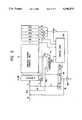
- FIG. 1is a block diagram of a first embodiment of the invention as a cache memory
- FIG. 2is a system configuration diagram showing how a microprocessor system is configured using the cache memory according to the invention
- FIG. 3is a circuit diagram showing how a data array, a gate and selector circuit and a full-write register are arranged in the cache memory according to the invention
- FIG. 4is a block diagram of a second embodiment of the invention as a cache memory
- FIG. 5is a system configuration diagram showing how a microprocessor system is configured using the cache memory of the second embodiment.
- FIG. 6is a diagram showing a configuration of a directory memory along with its peripheral circuits having a flag bit string which indicates whether any of the data in a data memory has been updated.
- FIG. 1depicts in a block diagram the first embodiment of the invention as a cache memory in a cache controller
- FIG. 2illustrates how a microprocessor system using this cache memory is configured.
- a cache memory 1 shown in FIG. 1is housed in a single chip on a semiconductor substrate.
- the memorythus constructed comprises an address array 11 as a directory memory, a data array 12 as a data memory, a block replacement control circuit 13 operating on the LRU (least recently used) algorithm, a tag comparator 14, a write buffer 15 which temporarily holds a write address and write data, and a control circuit 16 which controls the above circuits.
- the cache memory 1is installed between memory bus 21 to which a main memory 3 is connected, and an MPU bus 22.
- a 32-bit-long full-write register 19between the data array 12 and an internal data bus 17b via a gate and selector circuit 18.
- the address array 11contains, as a tag, high-order 10-plus bits of the main memory address for each data item in the same column position of the data array 12.
- An MPU 2supplies an address AD to the cache memory 1.
- a column address part CLM of that addressis fed to decoders of the address array 11 and data array 12, the corresponding address tag and data are read simultaneously from the same columns of both arrays.
- the data array 12is structured so that four-byte data is read at a time. Once read out, the data is placed temporarily in the full-write register 19.
- the address tag that was read from the address array 11is supplied to the tag comparator 14.
- the comparator 14is also supplied with the data of a tag part TAG of the address AD sent by the MPU 2.
- the tag from the address array 11 and the dataare then compared.
- a signal CHis output indicating whether the compare operation is a hit (match) or a miss (mismatch).
- the four-byte data that was read from the corresponding column position in the data array 12 and held in the full-write register 19is sent to the MPU 2 over the data bus 17b.
- the MPU 2gains direct access to the main memory 3 over the memory bus 21. If a miss is recognized during a data write operation, the address and the data held in the write buffer 15 are output onto the memory bus 21.
- the write buffer 15also functions as an address counter that generates a series of addresses needed for block transfer.
- the gate and selector circuit 18works as follows. A byte specification signal called a byte code (BC) is fed to the cache memory 1 from the MPU 2, a control signal is generated by the control circuit 16, and one-byte write data is set to the write buffer 15 during a data write operation. Using the control signal, the gate and selector circuit 18 stores selectively the write data in the full-write register 19 at its position corresponding to the byte code BC. At the same time, with one-word data having been read from the data array 12, the circuit 18 transfers to the full-write buffer 19 three bytes of the one-word data other than those bytes to be written. In addition, the gate and selector circuit 18 is structured so as to transfer the 32-bit data held in the full-write buffer 19 to both the data array 12 and the main memory 3, which is an external memory.
- BCbyte specification signal
- BCbyte code
- the memory buss 21is connected with a ROM 5 and an I/O register 6, as well as with a video data frame buffer 31, a file controller 32 and a DMA controller 33 via a system adapter 7.
- a memory control circuit 4is provided to control the data transfer between cache memory 1 and main memory 3.
- the memory control circuit 4is equipped with an ECC generator and an ECC checker, both not shown.
- An ECC codeof, say, 4 bits is generated and added to a 32-bit data item supplied from the cache memory 1.
- the datais stored in the main memory 3 along with the ECC code.
- the accompanying ECC codeis checked to correct an error bit as needed before the data is handed over to the cache memory 1.
- FIG. 3there is shown a typical circuit configuration of the data array 12, gate and selector circuit 18, and full-write register 19 in the cache memory whose block diagram is depicted in FIG. 1.
- the data array 12includes a dynamic RAM comprising single-element memory cells.
- this data arraywhich permits 32-bit parallel data read operations, there are provided 64 memory cell columns.
- the drain terminal of each of MOS Q's for selecting an odd-numbered column memory cellis connected to a common bit line BL; the drain terminal of each of MOS Q's for selecting an even-numbered column memory cell is connected to a common bit line BL.
- a total of 32 sense amplifiers SAare connected between the bit lines BL and BL.
- the gate terminals for the MOS Q's for selecting an odd-numbered column memory cellare connected to even-numbered word lines WL 2 and so on.
- the MOS Q's 32 memory cellsare turned on, causing the corresponding 32 sense amplifiers SA to read out one-word data simultaneously.
- each of the 64 bit lines BL and BLis divided into two branches.
- One branch lineis connected via two MOS gates Q 1 and Q 2 to latch circuits LT constituting the full-write register 19.
- the other branch lineis connected via MOS gates Q 3 to the same latch circuits LT.
- the data array 12is split into four blocks MB1 through MB4 in bytes, i.e., in eight bits.
- the bit lines BL' and BL'are connected with complementary output signal lines CO and CO of the write buffer 15.
- Each of the latch circuits LTis connected with a buffer that outputs latched data onto the data bus 17b shown in FIG. 1.
- the latch circuits LTmay be formed by differential amplifiers similar to the sense amplifiers SA of the data array 12.
- the MPU 2sends a byte control signal BC and eight-bit write data to the cache memory 1.
- the byte control signal BCis placed in the control circuit 16, while the eight-bit write data is set to predetermined eight buffer elements in the write buffer 15.
- the control circuit 16brings high only one control signal (Wi), out of the signals W 1 through W 4 for the MOS gate Q 2 , in order to select a block that corresponds to the specified byte. This causes the one-byte write data supplied by the MPU 2 to be written to the eight latch circuits LT corresponding to the byte code BC in the full-write register 19.
- the data array 12permits selection of the word line WL corresponding to the same column address CLM as that by which to retrieve the address array 11.
- an inverse signal Wi of the selection signal Witurns on the MOS gates Q 3 on the block that corresponds to the remaining three bytes to which write data (1 byte long) is not written. This causes the three bytes out of the four read from the data array 12 to be written to unoccupied latch circuits LT in the full-write register 19.
- a hit signal CHis output by the tag comparator 14. This brings high a control signal that corresponds to the byte control signal BC. That control signal is selected out of the signals H 1 through H 4 fed by the control circuit 16 to the MOS gates Q 1 . Bringing the control signal high turns on the MOS gates Q 1 connected to the latch circuits LT in which one-byte write data is held. The write data is then placed onto the bit lines of the data array 12, and is written to the selected memory cell by the sense amplifiers SA. Concurrently, the 32-bit data held by all the latch circuits LT is output to the external memory by buffers BFF via the data bus 17b .
- the selection signals W 1 through W 4 fed by the control circuit 16 to the gate and selector circuit 18are all brought to the selection level.
- the 32-bit write data held in the write buffer 15is written to all the latch circuits LT in the full-write register 19.
- a hit signal CHis output by the tag comparator 14, the 32 MOS gates Q 3 are all turned on.
- the one-word data in the full-write register 19is transferred both to the data array 12 and to the external memory via the buffer BFF.
- the first embodiment of the invention described aboveoperates on the so-called write-through method. Under this method, when any data item in the cache memory 1 is updated, the corresponding data item in the main memory 3 is updated simultaneoulsy.
- the circuitry of this embodimentcan also be applied to what is known as a copy-back cache memory. Under the copy-back method, when a block replacement occurs, the main memory is updated accordingly.
- the first embodiment of the inventionincludes a full-write register which can hold 32 bits of data at a time after a reading from a data array in a cache memory.
- the full-write registeris connected to the data array via gates.
- a selectoris provided between the full-write register on the one hand, and a write buffer holding write data or an internal bus arrangement on the other.
- the gates and the selectorare controlled in response to a byte control signal from a microprocessor unit (MPU).
- MPUmicroprocessor unit
- the updated 32-bit data in the full-write registeris at once stored in the data array and transferred to an external memory.
- the byte data subject to a partial-write operationcan be placed in the full-write register at the same time that data is read from the data array. This means that a partial-write operation may be performed on the data array in two cycles.
- a modified cache memory arrangementis one in which the 32-bit full-write register of the above-described embodiment may be replaced with a register capable of holding 64-bit or one-block (16-byte) data. Of the data thus held, four bytes are selected by a selector or the like for transfer to the main memory. Needless to say, the configuration of the gate and selector circuit that may be used in an eembodiment is not limited to what is depicted in FIG. 3.
- FIG. 4there will now be described the second embodiment of the invention as it is applied to a cache memory incorporated in a cache controller.
- This cache memorycan also be used in the microprocessor system shown in FIG. 2.
- a cache memory 1' shown in FIG. 4is housed in a single chip on a semiconductor substrate.
- the memorythus constructed comprises a directory memory 111, a data memory 112, a block replacement control circuit 113 operating on the LRU (least recently used) algorithm, tag comparators 114, a write buffer 115 which temporarily holds a write address and write data, and a control logic circuit 116 which controls the above circuits.
- LRUleast recently used
- a dualport block buffer 118capable of accommodating data of, say, 64 bytes per block.
- the cache memory of this embodimentadopts, but not limited to, the so-called set associative method whereby each block in the main memory is keyed to a plurality of blocks in the cache memory.
- the directory memory 111 and the data memory 112are each of a four-way type.
- the directory memory 111contains, as a tag, high-order 10-plus bits of the main memory address for each data item in the same column position of the data memory 112.
- the MPU 2supplies an address AD to the cache memory 1'.
- a column address part CLM of that addressis fed to decoders of the directory memory 111 and data memory 112
- the corresponding address tag and dataare read simultaneously from the same columns of both memories.
- the data memory 112is structured so that 16-byte data is read at a time. Once read out, the data is placed temporarily in the block buffer 118. Data transfer between data memory 112 and block buffer 118 is carried out in, but not limited to, 16 bytes.
- the address tag that was read from the directory memory 111is supplied to the tag comparators 114.
- the comparators 114are also supplied with the data of a tag part TAG in the address AD sent by the MPU.
- the tag from the directory memory 111 and the dataare then compared.
- a signal CHis output indicating whether the compare operation is a hit (match) or a miss (mismatch).
- the selectorselects the one-word (4-byte) data specified by the low-order two bits A 0 and A 1 of the current address out of the 16-byte data that was held in the block buffer 118 after being read from the corresponding position in the data memory 112.
- the selected datais supplied to the MPU 2 over the data bus 117b.
- the MPU bus 22 and the memory bus 21are connected via an internal address bus 117a and the internal data bus 117b. Using the memory bus 21, the MPU 2 gains direct access to the main memory 3. If a miss is recognized during a data write operation, the address that was read from the directory memory 111 is set to an address counter 119. The address is then incremented by a control signal coming from the control logic circuit 116. In this manner, a series of addresses are generated successively to provide for block transfer.
- the cache memory of the second embodimenthas a valid bit V and a block update bit BU.
- the valid bit Vindicates the validity of a block-length data item in that column position of the data memory which corresponds to each bit per column of the directory memory 111.
- the block update bit BUindicates whether there is any updated data item in each block. For this cache memory, one block has four words (16 bytes).
- the directory memory 111has data update bits DU1 through DU4. These bits indicate whether there is any updated word in the four words of data in each block.
- the flag bit V, BU, and DU1 through DU4 described aboveare read and supplied to the control logic circuit 116 at the same time that an address tag is read from the directory memory 111 based on the column address part CLM (A 2 through A 10 ) of an address AD of, say, 30 bits. The address is fed from the outside.
- the control logic circuit 116sets the bit V to "1" when one-block data is transferred from the main memory 111 to the data memory 112. If a write operation scores a hit in the cache memory and the corresponding data in the data memory 112 is updated accordingly, then a "1" is set on the bit DU that matches the one word specified by the lowest addresses A 0 and A 1 .
- Selecting one of the four data update bits DU1 through DU4is done by having a Y decoder Y-DEC (for decoding addresses A 0 and A 1 ) activate one of Y switches Y 1 through Y 4 .
- all the control logic circuit 116 has to dois to generate a write enable signal as well as the write data by which to set the data update bits (DU1-DU4) to "1" each in response to a cache hit signal HIT from the tag comparator 114.
- the signals that were read from the data update bits DU1 through DU4 upon read operationgo past the Y switches Y 1 through Y 4 before being OR'ed by a wired OR circuit to generate a logical sum signal DU.
- the logical sum signalis fed to the control logic circuit 116.
- the control logic circuit 116acts as follows. Without reading (i.e., abandoning) the block that is no longer needed, the circuit 116 latches onto the address counter 119 the address tag that was read from the directory memory 111 and the column address on the bus. By sending a count-up signal, the circuit 116 increments the address counter 119 to output addresses successively. Under the block transfer method, one block of data is transferred from the main memory to the cache memory for temporary storage in the block buffer 118. While the MPU 2 is not accessing the cache memory, the circuit 116 moves the block of data from the block buffer 118 to the data memory 112.
- the control logic circuit 116latches the address tag and the column address onto the address counter 119. Then if any of the data update bits DU1 through DU4 is "0," the circuit 116 counts up the address counter 119 at high speed. If any of the data update bits is "1,” the circuit 116 may, say, drive a tri-state buffer BBF to output to the outside the address from inside the address counter 119 and the corresponding data from inside the data memory 112. The address is retained long enough to permit writing to the main memory before the address counter 119 is incremented.
- the above-described arrangementprovides correspondence in content between main memory and cache memory. Because only the updated data in the cache memory is transferred, with the unchanged data left untouched, the time required for data transfer over the memory bus is substantially less than in conventional devices that transfer the entire block of data. As a result, the system throughput is improved.
- the second embodiment described aboveinvolves four words constituting a single block. It is to be noted that the number of words per block is not limited to four; it may be 8, 16 or otherwise. All that needs to be done in terms of per-block word count is to provide as many data update bits as required by the number of the words per block.
- the block buffer 118is provided between data array 112 and data bus 117b. In a modification, the block buffer 118 may be omitted. Alternatively, a bit may be provided to indicate if there exists effective data in the block buffer before data transfer occurs from the main memory to the data memory. In this case, a cache hit signal may also be generated so that the target data is read from the block buffer. This arrangement further boosts the processing speed.
- the second embodiment of the inventionincludes a bit string indicating whether or not any data in the data array has been updated in accordance with the tag in the address array acting as the directory memory.
- the bit stringis referenced so that only the updated data is transferred. Because each bit in the bit string corresponds to a word and not to a block for updating, the unchanged data need not be output to the outside. This improves the throughput of the memory bus and MPU bus.
- the four-way type set associative cache memory adopted in the second embodimentmay be replaced with a two-way type, five-way type or one that involves more than five ways.
- the inventioncan also be applied to a direct mapping cache memory.
Landscapes
- Engineering & Computer Science (AREA)
- Theoretical Computer Science (AREA)
- Databases & Information Systems (AREA)
- Microelectronics & Electronic Packaging (AREA)
- Computer Hardware Design (AREA)
- Physics & Mathematics (AREA)
- General Engineering & Computer Science (AREA)
- General Physics & Mathematics (AREA)
- Memory System Of A Hierarchy Structure (AREA)
Abstract
Description
Claims (8)
Priority Applications (1)
| Application Number | Priority Date | Filing Date | Title |
|---|---|---|---|
| US07/871,906US5202969A (en) | 1988-11-01 | 1992-04-21 | Single-chip-cache-buffer for selectively writing write-back and exclusively writing data-block portions to main-memory based upon indication of bits and bit-strings respectively |
Applications Claiming Priority (4)
| Application Number | Priority Date | Filing Date | Title |
|---|---|---|---|
| JP63-277624 | 1988-11-01 | ||
| JP63277624AJPH02122344A (en) | 1988-11-01 | 1988-11-01 | buffer storage |
| JP63-330040 | 1988-12-26 | ||
| JP63330040AJPH02171944A (en) | 1988-12-26 | 1988-12-26 | buffer storage |
Related Child Applications (1)
| Application Number | Title | Priority Date | Filing Date |
|---|---|---|---|
| US07/871,906DivisionUS5202969A (en) | 1988-11-01 | 1992-04-21 | Single-chip-cache-buffer for selectively writing write-back and exclusively writing data-block portions to main-memory based upon indication of bits and bit-strings respectively |
Publications (1)
| Publication Number | Publication Date |
|---|---|
| US5146573Atrue US5146573A (en) | 1992-09-08 |
Family
ID=26552479
Family Applications (1)
| Application Number | Title | Priority Date | Filing Date |
|---|---|---|---|
| US07/426,781Expired - LifetimeUS5146573A (en) | 1988-11-01 | 1989-10-25 | Single chip cache with partial-write circuit for transferring a preselected portion of data between memory and buffer register |
Country Status (2)
| Country | Link |
|---|---|
| US (1) | US5146573A (en) |
| KR (1) | KR900008516A (en) |
Cited By (27)
| Publication number | Priority date | Publication date | Assignee | Title |
|---|---|---|---|---|
| US5287512A (en)* | 1990-08-06 | 1994-02-15 | Ncr Corporation | Computer memory system and method for cleaning data elements |
| US5347643A (en)* | 1990-02-16 | 1994-09-13 | Hitachi, Ltd. | Bus system for coordinating internal and external direct memory access controllers |
| US5386540A (en)* | 1991-09-18 | 1995-01-31 | Ncr Corporation | Method and apparatus for transferring data within a computer using a burst sequence which includes modified bytes and a minimum number of unmodified bytes |
| US5420983A (en)* | 1992-08-12 | 1995-05-30 | Digital Equipment Corporation | Method for merging memory blocks, fetching associated disk chunk, merging memory blocks with the disk chunk, and writing the merged data |
| EP0661638A1 (en)* | 1993-12-28 | 1995-07-05 | International Business Machines Corporation | Method and apparatus for transferring data in a computer |
| US5448711A (en)* | 1990-06-07 | 1995-09-05 | Intel Corporation | Configuration apparatus for determining relative position of a cache memory in a cache memory array |
| US5491811A (en)* | 1992-04-20 | 1996-02-13 | International Business Machines Corporation | Cache system using mask bits to recorder the sequences for transfers of data through cache to system memory |
| US5511164A (en) | 1995-03-01 | 1996-04-23 | Unisys Corporation | Method and apparatus for determining the source and nature of an error within a computer system |
| US5530835A (en)* | 1991-09-18 | 1996-06-25 | Ncr Corporation | Computer memory data merging technique for computers with write-back caches |
| US5555391A (en)* | 1993-12-23 | 1996-09-10 | Unisys Corporation | System and method for storing partial blocks of file data in a file cache system by merging partial updated blocks with file block to be written |
| US5588012A (en)* | 1992-02-10 | 1996-12-24 | Fujitsu Limited | Apparatus and method for ensuring data in external storage system |
| US5680537A (en)* | 1995-03-01 | 1997-10-21 | Unisys Corporation | Method and apparatus for isolating an error within a computer system that transfers data via an interface device |
| US5784382A (en)* | 1995-03-01 | 1998-07-21 | Unisys Corporation | Method and apparatus for dynamically testing a memory within a computer system |
| US5784393A (en)* | 1995-03-01 | 1998-07-21 | Unisys Corporation | Method and apparatus for providing fault detection to a bus within a computer system |
| US5784712A (en)* | 1995-03-01 | 1998-07-21 | Unisys Corporation | Method and apparatus for locally generating addressing information for a memory access |
| US5828860A (en)* | 1992-10-16 | 1998-10-27 | Fujitsu Limited | Data processing device equipped with cache memory and a storage unit for storing data between a main storage or CPU cache memory |
| US5828823A (en)* | 1995-03-01 | 1998-10-27 | Unisys Corporation | Method and apparatus for storing computer data after a power failure |
| US5909701A (en)* | 1997-03-19 | 1999-06-01 | Micron Electronics | Interface for high speed memory |
| US5940826A (en)* | 1997-01-07 | 1999-08-17 | Unisys Corporation | Dual XPCS for disaster recovery in multi-host computer complexes |
| US5949970A (en)* | 1997-01-07 | 1999-09-07 | Unisys Corporation | Dual XPCS for disaster recovery |
| US6000013A (en)* | 1994-11-09 | 1999-12-07 | Sony Corporation | Method and apparatus for connecting memory chips to form a cache memory by assigning each chip a unique identification characteristic |
| US6233702B1 (en)* | 1992-12-17 | 2001-05-15 | Compaq Computer Corporation | Self-checked, lock step processor pairs |
| US6581142B1 (en)* | 2000-09-01 | 2003-06-17 | International Business Machines Corporation | Computer program product and method for partial paging and eviction of microprocessor instructions in an embedded computer |
| US20040162885A1 (en)* | 2003-02-18 | 2004-08-19 | Garg Sharad K. | Reducing communication for reads and updates in distributed object systems |
| US20090172363A1 (en)* | 2007-12-27 | 2009-07-02 | Doron Orenstien | Mixing instructions with different register sizes |
| US20090276562A1 (en)* | 2008-05-01 | 2009-11-05 | Sandisk Il Ltd. | Flash cache flushing method and system |
| US10108376B1 (en)* | 2017-05-04 | 2018-10-23 | Xilinx, Inc. | Memory initialization |
Citations (11)
| Publication number | Priority date | Publication date | Assignee | Title |
|---|---|---|---|---|
| US3820078A (en)* | 1972-10-05 | 1974-06-25 | Honeywell Inf Systems | Multi-level storage system having a buffer store with variable mapping modes |
| US3938097A (en)* | 1974-04-01 | 1976-02-10 | Xerox Corporation | Memory and buffer arrangement for digital computers |
| US4268907A (en)* | 1979-01-22 | 1981-05-19 | Honeywell Information Systems Inc. | Cache unit bypass apparatus |
| US4370710A (en)* | 1980-08-26 | 1983-01-25 | Control Data Corporation | Cache memory organization utilizing miss information holding registers to prevent lockup from cache misses |
| US4493026A (en)* | 1982-05-26 | 1985-01-08 | International Business Machines Corporation | Set associative sector cache |
| US4797813A (en)* | 1985-12-20 | 1989-01-10 | Kabushiki Kaisha Toshiba | Cache memory control apparatus |
| US4833642A (en)* | 1987-03-31 | 1989-05-23 | Nec Corporation | Cache controller giving versatility to cache memory structure |
| US4905188A (en)* | 1988-02-22 | 1990-02-27 | International Business Machines Corporation | Functional cache memory chip architecture for improved cache access |
| US4914582A (en)* | 1986-06-27 | 1990-04-03 | Hewlett-Packard Company | Cache tag lookaside |
| US4920478A (en)* | 1985-05-29 | 1990-04-24 | Kabushiki Kaisha Toshiba | Cache system used in a magnetic disk controller adopting an LRU system |
| US4970643A (en)* | 1988-03-07 | 1990-11-13 | Control Data Corporation | Mechanism for lock-up free cache operation with a remote address translation unit |
- 1989
- 1989-10-18KRKR1019890014987Apatent/KR900008516A/ennot_activeWithdrawn
- 1989-10-25USUS07/426,781patent/US5146573A/ennot_activeExpired - Lifetime
Patent Citations (11)
| Publication number | Priority date | Publication date | Assignee | Title |
|---|---|---|---|---|
| US3820078A (en)* | 1972-10-05 | 1974-06-25 | Honeywell Inf Systems | Multi-level storage system having a buffer store with variable mapping modes |
| US3938097A (en)* | 1974-04-01 | 1976-02-10 | Xerox Corporation | Memory and buffer arrangement for digital computers |
| US4268907A (en)* | 1979-01-22 | 1981-05-19 | Honeywell Information Systems Inc. | Cache unit bypass apparatus |
| US4370710A (en)* | 1980-08-26 | 1983-01-25 | Control Data Corporation | Cache memory organization utilizing miss information holding registers to prevent lockup from cache misses |
| US4493026A (en)* | 1982-05-26 | 1985-01-08 | International Business Machines Corporation | Set associative sector cache |
| US4920478A (en)* | 1985-05-29 | 1990-04-24 | Kabushiki Kaisha Toshiba | Cache system used in a magnetic disk controller adopting an LRU system |
| US4797813A (en)* | 1985-12-20 | 1989-01-10 | Kabushiki Kaisha Toshiba | Cache memory control apparatus |
| US4914582A (en)* | 1986-06-27 | 1990-04-03 | Hewlett-Packard Company | Cache tag lookaside |
| US4833642A (en)* | 1987-03-31 | 1989-05-23 | Nec Corporation | Cache controller giving versatility to cache memory structure |
| US4905188A (en)* | 1988-02-22 | 1990-02-27 | International Business Machines Corporation | Functional cache memory chip architecture for improved cache access |
| US4970643A (en)* | 1988-03-07 | 1990-11-13 | Control Data Corporation | Mechanism for lock-up free cache operation with a remote address translation unit |
Non-Patent Citations (4)
| Title |
|---|
| David A. Patterson, et al., "Computer Architecture A Quantitative Approach", 1990, pp. 403-425 and 454-474, (Provided in English). |
| David A. Patterson, et al., Computer Architecture A Quantitative Approach , 1990, pp. 403 425 and 454 474, (Provided in English).* |
| Nikkei Electronics, published by Nikkei McGraw Hill, Inc., Nov. 16, 1987, pp. 170 171, English translation provided.* |
| Nikkei Electronics, published by Nikkei-McGraw-Hill, Inc., Nov. 16, 1987, pp. 170-171, English translation provided. |
Cited By (31)
| Publication number | Priority date | Publication date | Assignee | Title |
|---|---|---|---|---|
| US5347643A (en)* | 1990-02-16 | 1994-09-13 | Hitachi, Ltd. | Bus system for coordinating internal and external direct memory access controllers |
| US5448711A (en)* | 1990-06-07 | 1995-09-05 | Intel Corporation | Configuration apparatus for determining relative position of a cache memory in a cache memory array |
| US5287512A (en)* | 1990-08-06 | 1994-02-15 | Ncr Corporation | Computer memory system and method for cleaning data elements |
| US5386540A (en)* | 1991-09-18 | 1995-01-31 | Ncr Corporation | Method and apparatus for transferring data within a computer using a burst sequence which includes modified bytes and a minimum number of unmodified bytes |
| US5530835A (en)* | 1991-09-18 | 1996-06-25 | Ncr Corporation | Computer memory data merging technique for computers with write-back caches |
| US5588012A (en)* | 1992-02-10 | 1996-12-24 | Fujitsu Limited | Apparatus and method for ensuring data in external storage system |
| US5491811A (en)* | 1992-04-20 | 1996-02-13 | International Business Machines Corporation | Cache system using mask bits to recorder the sequences for transfers of data through cache to system memory |
| US5420983A (en)* | 1992-08-12 | 1995-05-30 | Digital Equipment Corporation | Method for merging memory blocks, fetching associated disk chunk, merging memory blocks with the disk chunk, and writing the merged data |
| US5828860A (en)* | 1992-10-16 | 1998-10-27 | Fujitsu Limited | Data processing device equipped with cache memory and a storage unit for storing data between a main storage or CPU cache memory |
| US6233702B1 (en)* | 1992-12-17 | 2001-05-15 | Compaq Computer Corporation | Self-checked, lock step processor pairs |
| US5555391A (en)* | 1993-12-23 | 1996-09-10 | Unisys Corporation | System and method for storing partial blocks of file data in a file cache system by merging partial updated blocks with file block to be written |
| EP0661638A1 (en)* | 1993-12-28 | 1995-07-05 | International Business Machines Corporation | Method and apparatus for transferring data in a computer |
| US6000013A (en)* | 1994-11-09 | 1999-12-07 | Sony Corporation | Method and apparatus for connecting memory chips to form a cache memory by assigning each chip a unique identification characteristic |
| US5511164A (en) | 1995-03-01 | 1996-04-23 | Unisys Corporation | Method and apparatus for determining the source and nature of an error within a computer system |
| US5784382A (en)* | 1995-03-01 | 1998-07-21 | Unisys Corporation | Method and apparatus for dynamically testing a memory within a computer system |
| US5784393A (en)* | 1995-03-01 | 1998-07-21 | Unisys Corporation | Method and apparatus for providing fault detection to a bus within a computer system |
| US5828823A (en)* | 1995-03-01 | 1998-10-27 | Unisys Corporation | Method and apparatus for storing computer data after a power failure |
| US5680537A (en)* | 1995-03-01 | 1997-10-21 | Unisys Corporation | Method and apparatus for isolating an error within a computer system that transfers data via an interface device |
| US5784712A (en)* | 1995-03-01 | 1998-07-21 | Unisys Corporation | Method and apparatus for locally generating addressing information for a memory access |
| US5940826A (en)* | 1997-01-07 | 1999-08-17 | Unisys Corporation | Dual XPCS for disaster recovery in multi-host computer complexes |
| US5949970A (en)* | 1997-01-07 | 1999-09-07 | Unisys Corporation | Dual XPCS for disaster recovery |
| US5926838A (en)* | 1997-03-19 | 1999-07-20 | Micron Electronics | Interface for high speed memory |
| US5909701A (en)* | 1997-03-19 | 1999-06-01 | Micron Electronics | Interface for high speed memory |
| US6581142B1 (en)* | 2000-09-01 | 2003-06-17 | International Business Machines Corporation | Computer program product and method for partial paging and eviction of microprocessor instructions in an embedded computer |
| US20040162885A1 (en)* | 2003-02-18 | 2004-08-19 | Garg Sharad K. | Reducing communication for reads and updates in distributed object systems |
| US7266645B2 (en)* | 2003-02-18 | 2007-09-04 | Intel Corporation | Reducing communication for reads and updates in distributed object systems |
| US20090172363A1 (en)* | 2007-12-27 | 2009-07-02 | Doron Orenstien | Mixing instructions with different register sizes |
| US8694758B2 (en) | 2007-12-27 | 2014-04-08 | Intel Corporation | Mixing instructions with different register sizes |
| US20090276562A1 (en)* | 2008-05-01 | 2009-11-05 | Sandisk Il Ltd. | Flash cache flushing method and system |
| US9594679B2 (en)* | 2008-05-01 | 2017-03-14 | Sandisk Il Ltd. | Flash cache flushing method and system |
| US10108376B1 (en)* | 2017-05-04 | 2018-10-23 | Xilinx, Inc. | Memory initialization |
Also Published As
| Publication number | Publication date |
|---|---|
| KR900008516A (en) | 1990-06-04 |
Similar Documents
| Publication | Publication Date | Title |
|---|---|---|
| US5202969A (en) | Single-chip-cache-buffer for selectively writing write-back and exclusively writing data-block portions to main-memory based upon indication of bits and bit-strings respectively | |
| US5146573A (en) | Single chip cache with partial-write circuit for transferring a preselected portion of data between memory and buffer register | |
| US5416740A (en) | Semiconductor memory device including redundant memory cell array for repairing defect | |
| US5752260A (en) | High-speed, multiple-port, interleaved cache with arbitration of multiple access addresses | |
| KR940005684B1 (en) | Cash-embedded semiconductor device and its operation method | |
| US4426682A (en) | Fast cache flush mechanism | |
| US5226147A (en) | Semiconductor memory device for simple cache system | |
| US5574875A (en) | Cache memory system including a RAM for storing data and CAM cell arrays for storing virtual and physical addresses | |
| US6374325B1 (en) | Content addressable memory (CAM) | |
| US20040003315A1 (en) | Repairable block redundancy scheme | |
| US5717885A (en) | TLB organization with variable page size mapping and victim-caching | |
| US20040019763A1 (en) | Column/row redundancy architecture using latches programmed from a look up table | |
| US5396448A (en) | Associative memory system with hit entry detection circuit | |
| US5014240A (en) | Semiconductor memory device | |
| EP0689695B1 (en) | Fault tolerant memory system | |
| EP0523995A1 (en) | Integrated circuit memory device having flash clear | |
| US5060136A (en) | Four-way associative cache with dlat and separately addressable arrays used for updating certain bits without reading them out first | |
| US6295218B1 (en) | Semiconductor device | |
| US6603690B1 (en) | Low-power static column redundancy scheme for semiconductor memories | |
| US6525987B2 (en) | Dynamically configured storage array utilizing a split-decoder | |
| JPH07121439A (en) | Constituent body for usage of partially functional cache memory | |
| US6707752B2 (en) | Tag design for cache access with redundant-form address | |
| EP0523996B1 (en) | Integrated circuit memory device with redundant rows | |
| JP4004847B2 (en) | Associative memory device | |
| US5978245A (en) | Associative memory device having circuitry for storing a coincidence line output |
Legal Events
| Date | Code | Title | Description |
|---|---|---|---|
| AS | Assignment | Owner name:HITACHI, LTD., JAPAN Free format text:ASSIGNMENT OF ASSIGNORS INTEREST.;ASSIGNORS:SATO, KATSUYUKI;NISHIMUKAI, TADAHIKO;AOKI, HIROKAZU;AND OTHERS;REEL/FRAME:005996/0644 Effective date:19891019 Owner name:HITACHI VLSI ENGINEERING CORP., JAPAN Free format text:ASSIGNMENT OF ASSIGNORS INTEREST.;ASSIGNORS:SATO, KATSUYUKI;NISHIMUKAI, TADAHIKO;AOKI, HIROKAZU;AND OTHERS;REEL/FRAME:005996/0644 Effective date:19891019 Owner name:HITACHI, LTD., JAPAN Free format text:ASSIGNMENT OF ASSIGNORS INTEREST.;ASSIGNORS:OISHI, KANJI;FUKUTA, HIROSHI;KIKUCHI, TAKASHI;AND OTHERS;REEL/FRAME:005996/0640 Effective date:19891019 Owner name:HITACHI VLSI ENGINEERING CORP., JAPAN Free format text:ASSIGNMENT OF ASSIGNORS INTEREST.;ASSIGNORS:OISHI, KANJI;FUKUTA, HIROSHI;KIKUCHI, TAKASHI;AND OTHERS;REEL/FRAME:005996/0640 Effective date:19891019 | |
| STCF | Information on status: patent grant | Free format text:PATENTED CASE | |
| FEPP | Fee payment procedure | Free format text:PAYOR NUMBER ASSIGNED (ORIGINAL EVENT CODE: ASPN); ENTITY STATUS OF PATENT OWNER: LARGE ENTITY | |
| FPAY | Fee payment | Year of fee payment:4 | |
| FPAY | Fee payment | Year of fee payment:8 | |
| FPAY | Fee payment | Year of fee payment:12 |