US5146178A - Impedance-matched, class F high-frequency amplifier - Google Patents
Impedance-matched, class F high-frequency amplifierDownload PDFInfo
- Publication number
- US5146178A US5146178AUS07/759,565US75956591AUS5146178AUS 5146178 AUS5146178 AUS 5146178AUS 75956591 AUS75956591 AUS 75956591AUS 5146178 AUS5146178 AUS 5146178A
- Authority
- US
- United States
- Prior art keywords
- harmonic
- circuit
- output
- frequency
- impedance
- Prior art date
- Legal status (The legal status is an assumption and is not a legal conclusion. Google has not performed a legal analysis and makes no representation as to the accuracy of the status listed.)
- Expired - Lifetime
Links
- 239000010754BS 2869 Class FSubstances0.000titleabstractdescription20
- 230000005540biological transmissionEffects0.000claimsdescription34
- 239000003990capacitorSubstances0.000claims2
- 238000010586diagramMethods0.000description19
- 238000010276constructionMethods0.000description15
- 238000005094computer simulationMethods0.000description2
- 230000009466transformationEffects0.000description2
- 229910001218Gallium arsenideInorganic materials0.000description1
- 230000000903blocking effectEffects0.000description1
- 238000004891communicationMethods0.000description1
- 238000011960computer-aided designMethods0.000description1
- 230000003247decreasing effectEffects0.000description1
- 238000013461designMethods0.000description1
- 230000000694effectsEffects0.000description1
- 238000004806packaging method and processMethods0.000description1
- 230000000737periodic effectEffects0.000description1
- 238000012545processingMethods0.000description1
- 238000012360testing methodMethods0.000description1
Images


Classifications
- H—ELECTRICITY
- H03—ELECTRONIC CIRCUITRY
- H03F—AMPLIFIERS
- H03F3/00—Amplifiers with only discharge tubes or only semiconductor devices as amplifying elements
- H03F3/20—Power amplifiers, e.g. Class B amplifiers, Class C amplifiers
- H03F3/21—Power amplifiers, e.g. Class B amplifiers, Class C amplifiers with semiconductor devices only
- H03F3/217—Class D power amplifiers; Switching amplifiers
- H03F3/2176—Class E amplifiers
- H—ELECTRICITY
- H03—ELECTRONIC CIRCUITRY
- H03F—AMPLIFIERS
- H03F3/00—Amplifiers with only discharge tubes or only semiconductor devices as amplifying elements
- H03F3/20—Power amplifiers, e.g. Class B amplifiers, Class C amplifiers
- H03F3/21—Power amplifiers, e.g. Class B amplifiers, Class C amplifiers with semiconductor devices only
- H03F3/217—Class D power amplifiers; Switching amplifiers
- H03F3/2171—Class D power amplifiers; Switching amplifiers with field-effect devices
Definitions
- This inventionrelates to a high-frequency amplifier.
- High-frequency amplifiersare used as power amplifiers for communication systems which transmit and receive high-frequency signals.
- This inventionrelates, more particularly, to a high-frequency amplifier with a high power efficiency.
- the power efficiencyis represented by the ratio of a high-frequency output power against the supplied D.C. power.
- a class-F amplifieris formed by adding a harmonic processing circuit to a class-B amplifier to increase power efficiency in a high-frequency amplifier.
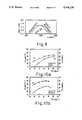
- FIG. 12shows an operating principle of the class-F amplifier.
- a FETis used as an active device in the following description, but the same effect is obtained when a bipolar transistor or an electron tube is used.
- the horizontal axisrepresents time t
- the vertical axisdrain volta V d and drain current i d .
- the time waveform of the drain voltage V dis expressed with a broken line while that of the drain current is expressed with a solid line.
- the time waveform of the drain voltage V dbecomes a square wave which is represented by the fundamental waveform and the odd harmonic frequency component.
- the time waveform of the drain current i dthen becomes a periodic half-wave which is represented by the fundamental wave and the even harmonic component. Therefore, when the drain current i d is passing, the drain volta V d becomes zero. Conversely, when the drain voltage is not zero, the drain current i d is not being passed. This makes the power consumption between the drain and the source zero, to thereby increase the power efficiency.
- the power efficiency ⁇ of a power amplifiercan be expressed by the ratio of the high frequency output power P RFout against the input DC power P DC inputted between the drain and the source. If expressed in percentage, the relation holds as below.
- P dissis the power consumed by the power amplifier. If P diss is made zero, the power efficiency ⁇ becomes 100%.
- FIG. 11is a block diagram to show an example of an ideal construction of a prior art class-F amplifier wherein a signal input at an input terminal 81 from a input transmission line is supplied to a gate terminal of a FET 85 via an input matching circuit 84.
- the source terminal S of the FET 85is grounded, and the output signal is transmitted from a drain terminal D to an output terminal 82 via an output matching circuit 86 and then to be outputted to the output transmission line.
- An even harmonic terminating circuit 88is connected to the drain terminal D of the FET 85 in the class-F amplifier.
- the input matching circuit 84is a circuit for impedance transformation, and realizes impedance matching between the output impedance of the input transmission line and the input impedance of the FET 85 for an input signal of the fundamental frequency f 0 .
- the output matching circuit 86is also a circuit for impedance transformation, but it realizes the impedance matching between the output impedance of the FET 85 and the impedance of the output transmission line at the fundamental frequency f 0 .
- the output matching circuit 86is designed to have a high impedance for the harmonic frequency.
- the even harmonic terminating circuit 88has impedance characteristics which make the circuit an open circuit for the fundamental frequency and the odd harmonic frequency but short-circuited for the even harmonic frequency.
- the input matching circuitsare typically passive L-C circuits. Therefore, the impedance frequency characteristics of the load at the output (drain) of the FET 85 are such that the impedance becomes matched at the fundamental frequency, short-circuited at the even harmonic frequencies and open at the odd harmonic
- the circuitis therefore usually constructed so as to be substantially short-circuited only for the second harmonic frequency, which has the largest power of all the even harmonic frequencies, and the even harmonic frequencies of the fourth or higher degrees are generally ignored. Since the odd harmonic frequencies are terminated to a high impedance, the even harmonic frequencies of the fourth or higher degrees are also frequently loaded with a high impedance. These circuits could provide a practically sufficient efficiency.
- FIG. 13shows a specific example of circuit structure of a prior art class-F amplifier using a FET.
- the same component partsare denoted with the same reference numerals as in FIG. 11.
- the FET 85is shown modeled as a FET device which is an ideal active device, and a reactance which is caused by wire-bonding, package characteristics, etc. and impedance of the chip itself.
- FIG. 13shows an equivalent circuit of the impedance as a reactance circuit 96 with inductance L and capacitance C.
- three terminals of a practical device, FET 85are referred to as a gate terminal, a drain terminal and a source terminal while those for an ideal FET are referred to simply as a gate, a drain and a source.
- the gate terminal of FET 85is supplied with a gate bias from a gate voltage supply terminal 91 via a choke coil 93g and an input matching circuit 84.
- the drain terminal of the FET 85is supplied with a drain bias from a drain voltage V d supply terminal 92 via a choke coil 93d.
- Condensers 94i and 94oare inserted respectively between the input terminal 81 and the input matching circuit 84 and between the output matching circuit 86 and the output terminal 82 in order to block direct current.
- a second harmonic terminating circuit 95comprises a series resonance circuit with inductance L and capacitance C so as to make the input impedance high at the fundamental frequency f 0 and short-circuited at the second harmonic frequency.
- the output matching circuit 86is a low-pass filter with inductance L and capacitance C and is designed to match the output transmission line with the input impedance of the FET 85 at the fundamental frequency and to have a high input impedance at the second harmonic frequency.
- the impedance which is shown by the reactance circuit 96exists not only at the fundamental frequency but also at the second harmonic frequency.
- the load impedanceis a combination of the two impedances of the second harmonic terminating circuit 95 and of the reactance circuit 96 at the second harmonic frequency. Therefore, even if the second harmonic terminating circuit resonates at the second harmonic frequency, the load when viewed from the drain is not usually short-circuited at the resonating impedance, and it is very difficult to realize the expected power efficiency.
- This inventionaims to provide a high-frequency amplifier with a high power efficiency at harmonic frequencies which is not affected by various type of stray reactance caused by the structure of the active devices or by the packaging configuration.
- this inventionprovides a high-frequency amplifier comprising an active device which amplifies a fundamental frequency of input high frequency signals in power and an output circuit which is inserted between an output of the active device and an output transmission on lines, the output circuit including an output matching circuit for matching the output from the active device with the output transmission line in impedance and an even harmonic terminating circuit which is designed to have high input impedance for the fundamental frequency and low input impedance for at least the second harmonic frequency thereof.
- the output matching circuitis configured to impedance match not only for the fundamental frequency but also for the second harmonic frequency thereof.
- the high frequency amplifier according to this inventionhas an even harmonic terminating circuit which is connected to the output side of the output matching circuit.
- impedance matching used hereinmeans that two impedance circuits which are connected with each other in complex conjugates.
- the even harmonic terminating circuitis preferably configured to have high input impedance for odd harmonic frequencies of the fundamental frequency. It is preferable that a reactance circuit be provided between the even harmonic terminating circuit and the output transmission line to have a high input impedance for the second harmonic frequency.
- the output matching circuitmay be configured to have a high input impedance for the third harmonic frequency or may achieve impedance matching for the third harmonic frequency.
- the even harmonic terminating circuitshould be structured to have high input impedance for the third harmonic frequency and a reactance circuit should be provided between the even harmonic terminating circuit and the output transmission line to achieve high input impedance for the third harmonic frequency thereof.
- a terminating circuit for the second harmonic being short-circuitedis provided in the succeeding stage of the output matching circuit which is configured to impedance match not only for the fundamental frequency but also for the second harmonic frequency thereof. This prevents the reactance presence at the output terminal of the active device from influencing the short-circuit conditions of the second harmonic. Therefore, the short-circuit conditions for the second harmonic frequency can be realized highly precisely as the output load on the active device, to thereby improve the power efficiency.
- the input impedancebecomes high for the second harmonic frequency, and therefore, the short-circuit load conditions for the second harmonic can be determined at a still higher precision to attain a higher power efficiency.
- the output matching circuitWhen the input impedance of the output matching circuit is set high for the third harmonic frequency, as the output matching circuit itself can realize open load conditions for the third harmonic, a power efficiency can be obtained at a level still higher than the case when the second harmonic frequency alone is used.
- the third harmonic frequencyis matched by the output matching circuit, because open impedance conditions can be determined in the succeeding stage of the even harmonic terminating circuit, the influence from the reactance on the output of the active device can be similarly avoided. More particularly, in addition to the short-circuit load conditions for the second harmonic, the open load conditions for the third harmonic can be realized at a higher precision, to thereby further improve the power efficiency.
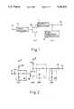
- FIG. 1is a block diagram to show the basic construction of this invention.
- FIG. 2is a circuit diagram to show the first embodiment of this invention.
- FIG. 3is a circuit diagram to show the second embodiment of this invention.
- FIG. 4is a circuit diagram to show the third embodiment of this invention.
- FIG. 5is a circuit diagram to show the fourth embodiment of this invention.
- FIG. 6is a circuit diagram to show the fifth embodiment of this invention.
- FIG. 7is a circuit diagram to show the sixth embodiment of this invention.
- FIG. 8is a circuit diagram to show the seventh embodiment of this invention.
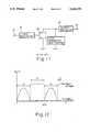
- FIG. 9is a graph to show the result of computer simulation of gain characteristics.
- FIGS. 10a and 10bare graphs to show the characteristics relative to the output power P 0 against the input power P i of an amplifier of the embodiments of this invention.
- FIG. 11is a block diagram to show an ideal example of the construction of prior art class-F amplifier.
- FIG. 12is a graph to show the operation principle of a class-F amplifier.
- FIG. 13is a circuit diagram to show a specific circuit construction of a prior art class-F amplifier using a FET.
- FIG. 1is a block diagram to show the basic construction of this invention.
- the inventionincludes an input terminal 81, an output terminal 82, an input matching circuit 84, a FET 85 and an even harmonics terminating circuit 88 which are similar to the corresponding circuits of the prior art class-F amplifier shown in FIG. 11.
- the amplifier of this embodimentalso includes an output matching circuit 11 which is constructed to match the impedance of the output from the FET 85 with that of the output transmission line connected to the output terminal 82 not only for the fundamental frequency but also for the second harmonic frequency thereof, and an even harmonic terminating circuit 88 is connected to the output side of the output matching circuit 11.
- the input matching circuit 84, the output matching circuit 11, and even harmonic terminating circuit 88may be constructed with lumped constant elements such as inductances and capacitances or distributed constant elements using microstrip lines. Structures with lumped constant elements will be described in the following explanation for illustration.
- FIG. 2is a circuit diagram to show the first embodiment of this invention wherein the output matching circuit 11 has an inductance L and capacitance C.
- the element constants of L and Care selected to match in conjugate the output impedance of the FET 85 with the impedance of the output transmission line for the fundamental frequency and the second harmonic frequency.
- the inductance Lis serially connected to the output transmission line while the capacitance C is connected in parallel to the load, but the characteristics necessary for the circuit 11 are those related to conjugate matching alone, and positions of the connections of L and of C may be reversed in selecting the element constants.
- the reactance component at the output impedance of the FET 85is offset by the output matching circuit 11 of the above structure, the real reactance to be connected to the drain terminal of the FET 85 becomes the second harmonic terminating circuit 95 along.
- the second harmonic terminating circuit 95is configured to short-circuit and resonate at the second harmonic frequency, short-circuit load conditions can be determined precisely for the second harmonic at the drain terminal of the FET 85 without being influenced by various types of stray reactance in the FET 85.
- the load conditionscan be determined very precisely for the second harmonic which is most important to the voltage/current waveforms necessary to operate an ideal class-F amplifier shown in FIG. 12 to thereby achieve a high efficiency.
- FIG. 3is a circuit diagram to show the second embodiment of this invention.
- This embodimenthas a parallel resonant circuit 21 with inductance L and capacitance C inserted between the second harmonic terminating circuit 95 and the output terminal 82.
- the circuit 21is set to have an element constant to resonate at the second harmonic frequency. This makes the impedance viewed from the side of the second harmonic terminating circuit 95 extremely high at a level which could be regarded as almost open at the second harmonic frequency.
- the second harmonic terminating circuit 95serially resonates at the second harmonic frequency to make its impedance extremely low.
- an output matching circuit 11'having an inductance and capacitance L and C at positions reversed to those of the circuit 11 shown in FIG. 2 is used.
- the condenser f 0 in FIG. 2is not necessary for preventing direct current.
- the load of the FET 85 at the second harmonic frequencyis given as a parallel impedance of the resonant impedance of the second harmonic terminating circuit 95 and the impedance of the output transmission line.
- the impedance on the side of the output transmission linebecomes extremely high compared to the second harmonic frequency when viewed from the circuit 95. This reduces influence on the resonance characteristics of the second harmonic terminating circuit 95 caused by the connection with the output transmission line. Accordingly, the load conditions of the FET 85 for the second harmonic can be determined more closely to the ideal conditions for the operating conditions of the class-F amplifier to further improve the power efficiency.
- FIG. 4is a circuit diagram to show the third embodiment of this invention which is different from the second embodiment in that a low pass filter 22 having inductances L and capacitances C in two-stage construction is used as the reactance circuit inserted between the second harmonic terminating circuit 95 and the output terminal 82.
- the element constants of L and C which constitute the low pass filter 22are set to have characteristics which pass the fundamental frequency with low loss and yet break at the second harmonic frequency with high impedance.
- the high impedance conditionswhich are realized in the structure shown in FIG. 3 by means of the parallel resonance circuit 21 are achieved by the low pass filter 22 for the second harmonic frequency.
- this inventionmay be alternately embodied by means of a low pass filter of one- or three-stage construction.
- FIG. 5is a circuit diagram to show the fourth embodiment of this invention wherein the output matching circuits 11, 11' used in the above two embodiments are replaced with an output matching circuit 31.
- the circuit 31comprises inductance L and capacitance C of which element constants are selected so that the output of the FET 85 is matched in conjugate with the output transmission line not only for the fundamental frequency and the second harmonic frequency but also for a third harmonic frequency.
- the output matching circuit 31is shown to have a construction equivalent to the circuit 11' of the aforementioned embodiment, the construction is not necessarily the same depending on the characteristics of the active device. As the circuit 31 allows the third harmonic frequency to pass, it is required to have a reactance circuit which becomes a high impedance for the third harmonic frequency at the succeeding stage.
- a parallel resonant circuit 32 with inductance L and capacitance Cis used.
- the L and C of the parallel resonant circuit 32have element constants selected to resonate at the third harmonic frequency. Therefore, when viewed from the output matching circuit 3-, the output transmission line is open at the third harmonic frequency.
- the second harmonic terminating circuit 95is short-circuited and resonates at the second harmonic frequency and shows the open characteristics of high impedance at other frequencies.
- the output load impedance characteristics at the drain terminal of the FET 85is load-matched at the fundamental frequency, short-circuited at the second harmonic frequency and open at the third harmonic frequency. More particularly, the load conditions required for the operation of class-F amplifier are realized not only at the second harmonic but also at the third harmonic to achieve a higher efficiency than above two embodiments.
- the parallel resonance circuit 32may be replaced with the low pass filter shown in FIG. 4.
- FIG. 6shows a circuit diagram of the fifth embodiment of this invention wherein the reactance circuit 31 which satisfies the matching conditions not only for the fundamental frequency and the second harmonic frequency but also for the third harmonic frequency and the output transmission line is formed by a low pass filter 41 of a two-stage construction comprising inductance L and capacitance C.
- the element constants of L and Care set so as to pass at the fundamental frequency with low loss and to break at the second and third harmonic frequencies with high impedance. As this has a high impedance for the second harmonic frequency, it has little influence on the resonance characteristics of the second harmonic terminating circuit 95. Therefore, the load conditions of the FET 85 for the second and third harmonics can be made closer to the ideal conditions of a class-F amplifier to thereby enhance the power efficiency.
- FIG. 7is a circuit diagram to show the sixth embodiment of this invention.
- an output matching circuit 51which assumes a high impedance, instead of matching, at the third harmonic frequency.
- the circuit 51comprises inductance L and capacitance C which have an element constant each of which matches in conjugate between the output transmission line at the fundamental frequency and the second harmonic frequency, and have high input impedance characteristics at the third harmonic frequency.
- the characteristics to make high input impedance at the third harmonic frequencymay be realized by the parallel resonant circuit 52 comprising L and C.
- the second harmonic terminating circuit 95is constructed to short-circuit and resonate at the second harmonic frequency and to have high impedance at other frequencies as described above. Therefore, the output load impedance characteristics of the drain terminal of the FET 85 are made to have matched loads at the fundamental frequency, be short-circuited at the second harmonic and open at the third harmonic to thereby satisfy the load conditions required for the operation of a class-F amplifier at the second and third harmonic frequencies and to achieve a higher power efficiency.
- FIG. 8is a circuit diagram to show the seventh embodiment of this invention. This embodiment is obtained by adding a parallel resonant circuit 21 which becomes open at the second harmonic frequency to the structure of the sixth embodiment shown in FIG. 7. It can realize low impedance characteristics that are closer to the short-circuit conditions as the load impedance conditions at the second harmonic frequency.
- the parallel resonance circuit 21may be replaced with the low pass filter shown in FIG. 4.
- a condenser 94 for blocking DCis connected at the stage preceding the transmission line.
- FIG. 9shows the result of a computer simulation of gain characteristics on a modeled one-stage amplifier using a standard packaged GaAs FET.
- the horizontal axisshows the frequency (in the unit of MHz) and the vertical axis shows the gain (in the unit of dB).
- this invention embodimentsdid not show a decrease in gain as shown with the bold line (2 GHz).
- the 0.5 dB decrease in gainleads to about an 8% decrease in efficiency if the amplifier of the gain 10 dB has 70% power added efficiency ⁇ add (P 0 -P i /P DC ⁇ 100), wherein the input power is denoted with P i , output power with P i , and the DC consumption power of the transistor with P DC . Decrease in gain is more marked as the frequency increases.
- FIGS. 10a and 10bshow characteristics of the input power P i and the output power P o of the amplifier of this embodiment.
- FIG. 10ashows the characteristics of the embodiment with a 2 GHz amplifier while
- FIG. 10bshows that of the embodiment with a 400 MHz amplifier.
- a sufficiently high gaincan be obtained with a Si bipolar transistor at 400 MHz as long as the transistor is used as an active device.
- the output matching circuitis realized with one-stage construction in the above embodiments, a multi-stage construction may be utilized to realize the predetermined matching conditions for higher efficiency.
Landscapes
- Engineering & Computer Science (AREA)
- Power Engineering (AREA)
- Amplifiers (AREA)
- Microwave Amplifiers (AREA)
Abstract
Description
=(P.sub.RFout /P.sub.DC)×100
=((P.sub.DC -P.sub.diss)/P.sub.dC)×100
Claims (20)
Applications Claiming Priority (2)
| Application Number | Priority Date | Filing Date | Title |
|---|---|---|---|
| JP2312503AJPH0732335B2 (en) | 1990-11-16 | 1990-11-16 | High frequency amplifier |
| JP2-312503 | 1990-11-16 |
Publications (1)
| Publication Number | Publication Date |
|---|---|
| US5146178Atrue US5146178A (en) | 1992-09-08 |
Family
ID=18030003
Family Applications (1)
| Application Number | Title | Priority Date | Filing Date |
|---|---|---|---|
| US07/759,565Expired - LifetimeUS5146178A (en) | 1990-11-16 | 1991-09-13 | Impedance-matched, class F high-frequency amplifier |
Country Status (2)
| Country | Link |
|---|---|
| US (1) | US5146178A (en) |
| JP (1) | JPH0732335B2 (en) |
Cited By (85)
| Publication number | Priority date | Publication date | Assignee | Title |
|---|---|---|---|---|
| US5270668A (en)* | 1991-03-27 | 1993-12-14 | Mitsubishi Denki Kabushiki Kaisha | Semiconductor amplifier |
| US5300895A (en)* | 1992-10-01 | 1994-04-05 | Texas Instruments Incorporated | Method for terminating harmonics of transistors |
| US5329249A (en)* | 1993-10-13 | 1994-07-12 | Pacific Monolithics, Inc. | High efficiency RF power amplifier |
| US5347229A (en)* | 1991-12-16 | 1994-09-13 | Texas Instruments Incorporated | Power amplifier with harmonically trapped heterojunction bipolar transistor |
| WO1995002277A1 (en)* | 1993-07-07 | 1995-01-19 | Wireless Access, Inc. | Stable, narrow bandwidth, high frequency amplifier with low power consumption |
| US5412347A (en)* | 1992-12-03 | 1995-05-02 | U.S. Philips Corporation | Compact cascadable microwave amplifier circuits |
| US5457427A (en)* | 1994-04-29 | 1995-10-10 | Philips Electronics North America Corporation | High-frequency amplifier means with enhanced output resistance |
| US5469107A (en)* | 1992-07-22 | 1995-11-21 | Mitsubishi Denki Kabushiki Kaisha | Microwave amplifier |
| US5535438A (en)* | 1994-05-10 | 1996-07-09 | Panasonic Technologies, Inc. | Phase linear class E amplifier for a satellite communication terminal which communicates with a low earth orbiting satellite |
| US5551075A (en)* | 1991-10-18 | 1996-08-27 | U.S. Philips Corporation | Semiconductor device including a plurality of interconnected functional integrated circuit blocks operating at high and ultrahigh frequencies, each having a DC distribution line |
| US5886595A (en)* | 1996-05-01 | 1999-03-23 | Raytheon Company | Odd order MESFET frequency multiplier |
| US5905409A (en)* | 1997-03-13 | 1999-05-18 | Mitsubishi Denki Kabushiki Kaisha | Microwave and millimeter wave circuit including amplifier and band elimination filters |
| US5939939A (en)* | 1998-02-27 | 1999-08-17 | Motorola, Inc. | Power combiner with harmonic selectivity |
| US6052033A (en)* | 1998-09-30 | 2000-04-18 | Logitech, Inc. | Radio frequency amplifier system and method |
| US6121840A (en)* | 1996-12-24 | 2000-09-19 | Murata Manufacturing Co., Ltd. | High-frequency amplifier |
| US6177841B1 (en)* | 1998-09-28 | 2001-01-23 | Mitsubishi Denki Kabushiki Kaisha | High frequency power amplifier |
| US6249186B1 (en)* | 1998-04-10 | 2001-06-19 | Taiyo Yuden Co., Ltd. | High-frequency power amplifier circuit and high-frequency power amplifier module |
| WO2001059927A1 (en)* | 2000-02-08 | 2001-08-16 | Mitsubishi Denski Kabushiki Kaisha | Multistage amplifier |
| CN1084548C (en)* | 1997-05-20 | 2002-05-08 | 松下电器产业株式会社 | High frequency amplifier with guard circuit and radio wave transmission apparatus including the same |
| US6388527B1 (en) | 1997-11-27 | 2002-05-14 | Nec Corporation | Semiconductor circuit with a stabilized gain slope |
| US20020118067A1 (en)* | 2001-02-23 | 2002-08-29 | Nec Corporation | Analog amplifier circuit |
| WO2002047256A3 (en)* | 2000-12-07 | 2003-01-03 | Ericsson Inc | Harmonic matching network for a saturated amplifier |
| CN1099755C (en)* | 1997-10-29 | 2003-01-22 | 日本电气株式会社 | Microwave amplifier for reducing pulsating noise |
| US6538515B2 (en) | 2001-01-19 | 2003-03-25 | Telefonaktiebolaget Lm Ericsson (Publ) | Power amplifier and method of operating a power amplifier having multiple output-power modes |
| WO2003043181A3 (en)* | 2001-11-15 | 2003-10-16 | Filtronic Plc | Class-f amplifier using an lc output filter network |
| US6724255B2 (en) | 2000-10-10 | 2004-04-20 | California Institute Of Technology | Class E/F switching power amplifiers |
| US6750711B2 (en)* | 2001-04-13 | 2004-06-15 | Eni Technology, Inc. | RF power amplifier stability |
| US6759908B2 (en)* | 2000-11-29 | 2004-07-06 | Mitsubishi Denki Kabushiki Kaisha | High frequency power amplifier |
| US20050151484A1 (en)* | 2003-05-27 | 2005-07-14 | Disney Donald R. | Electronic circuit control element with tap element |
| US20050275454A1 (en)* | 2002-03-11 | 2005-12-15 | Seyed-Ali Hajimiri | Cross-differential amplifier |
| US20050282503A1 (en)* | 2004-06-21 | 2005-12-22 | M/A-Com, Inc. | Combined matching and filter circuit |
| US20060176114A1 (en)* | 2005-02-10 | 2006-08-10 | Raytheon Company | Broadband microwave amplifier |
| US20060270367A1 (en)* | 2004-06-23 | 2006-11-30 | Burgener Mark L | Integrated RF front end with stacked transistor switch |
| US20060279362A1 (en)* | 2005-06-08 | 2006-12-14 | Sheng-Fuh Chang | Concurrent triple-band gain amplifier for multi-standard coexist communications |
| RU2306667C1 (en)* | 2005-12-22 | 2007-09-20 | Александр Владимирович Баранов | Switching power amplifier |
| US20080180170A1 (en)* | 2007-01-25 | 2008-07-31 | Research In Motion Limited | System and method for controlling radio frequency transmissions from an electronic device |
| US20080204139A1 (en)* | 2000-10-10 | 2008-08-28 | Abbas Komijani | Reconfigurable distributed active transformers |
| US20080252382A1 (en)* | 2007-04-12 | 2008-10-16 | Kabushiki Kaisha Toshiba | Class-f power amplifier circuit |
| US20090015328A1 (en)* | 2007-07-11 | 2009-01-15 | Axiom Microdevices, Inc. | Low offset envelope detector and method of use |
| US20090179714A1 (en)* | 2006-06-19 | 2009-07-16 | Ali-Ahmad Walid Y | Harmonic Termination Of Power Amplifiers Using BAW Filter Output Matching Circuits |
| RU2393624C1 (en)* | 2008-12-11 | 2010-06-27 | Александр Владимирович Баранов | Key power amplifier |
| US7860499B2 (en) | 2001-10-10 | 2010-12-28 | Peregrine Semiconductor Corporation | Switch circuit and method of switching radio frequency signals |
| CN102098009A (en)* | 2010-12-20 | 2011-06-15 | 芯通科技(成都)有限公司 | Output match circuit of radio frequency (RF) power amplifier and design method thereof |
| US20110140784A1 (en)* | 2009-12-16 | 2011-06-16 | Auriga Measurement Systems, LLC | Amplifier Circuit |
| US20110156819A1 (en)* | 2008-07-18 | 2011-06-30 | Tae Youn Kim | Low-Noise High Efficiency Bias Generation Circuits and Method |
| US8049563B2 (en) | 2000-10-10 | 2011-11-01 | California Institute Of Technology | Distributed circular geometry power amplifier architecture |
| US8378736B2 (en) | 2003-09-08 | 2013-02-19 | Peregrine Semiconductor Corporation | Low noise charge pump method and apparatus |
| US8405147B2 (en) | 2005-07-11 | 2013-03-26 | Peregrine Semiconductor Corporation | Method and apparatus for use in improving linearity of MOSFETs using an accumulated charge sink |
| US20130181788A1 (en)* | 2012-01-17 | 2013-07-18 | Richwave Technology Corp. | Matching circuit system |
| US8536636B2 (en) | 2007-04-26 | 2013-09-17 | Peregrine Semiconductor Corporation | Tuning capacitance to enhance FET stack voltage withstand |
| US8604864B2 (en) | 2008-02-28 | 2013-12-10 | Peregrine Semiconductor Corporation | Devices and methods for improving voltage handling and/or bi-directionality of stacks of elements when connected between terminals |
| US20130335147A1 (en)* | 2010-10-20 | 2013-12-19 | Nanyang Technological University | Power Amplifier and Linearization Techniques Using Active and Passive Devices |
| US8686787B2 (en) | 2011-05-11 | 2014-04-01 | Peregrine Semiconductor Corporation | High voltage ring pump with inverter stages and voltage boosting stages |
| US8723260B1 (en) | 2009-03-12 | 2014-05-13 | Rf Micro Devices, Inc. | Semiconductor radio frequency switch with body contact |
| US8729952B2 (en) | 2012-08-16 | 2014-05-20 | Triquint Semiconductor, Inc. | Switching device with non-negative biasing |
| US8742502B2 (en) | 2005-07-11 | 2014-06-03 | Peregrine Semiconductor Corporation | Method and apparatus for use in improving linearity of MOSFETs using an accumulated charge sink-harmonic wrinkle reduction |
| US8829967B2 (en) | 2012-06-27 | 2014-09-09 | Triquint Semiconductor, Inc. | Body-contacted partially depleted silicon on insulator transistor |
| US8847672B2 (en) | 2013-01-15 | 2014-09-30 | Triquint Semiconductor, Inc. | Switching device with resistive divider |
| US8923782B1 (en) | 2013-02-20 | 2014-12-30 | Triquint Semiconductor, Inc. | Switching device with diode-biased field-effect transistor (FET) |
| US8954902B2 (en) | 2005-07-11 | 2015-02-10 | Peregrine Semiconductor Corporation | Method and apparatus improving gate oxide reliability by controlling accumulated charge |
| US8977217B1 (en) | 2013-02-20 | 2015-03-10 | Triquint Semiconductor, Inc. | Switching device with negative bias circuit |
| US9203396B1 (en) | 2013-02-22 | 2015-12-01 | Triquint Semiconductor, Inc. | Radio frequency switch device with source-follower |
| US9214932B2 (en) | 2013-02-11 | 2015-12-15 | Triquint Semiconductor, Inc. | Body-biased switching device |
| US9264053B2 (en) | 2011-01-18 | 2016-02-16 | Peregrine Semiconductor Corporation | Variable frequency charge pump |
| US9379698B2 (en) | 2014-02-04 | 2016-06-28 | Triquint Semiconductor, Inc. | Field effect transistor switching circuit |
| US9397656B2 (en) | 2005-07-11 | 2016-07-19 | Peregrine Semiconductor Corporation | Circuit and method for controlling charge injection in radio frequency switches |
| US9406695B2 (en) | 2013-11-20 | 2016-08-02 | Peregrine Semiconductor Corporation | Circuit and method for improving ESD tolerance and switching speed |
| US9419565B2 (en) | 2013-03-14 | 2016-08-16 | Peregrine Semiconductor Corporation | Hot carrier injection compensation |
| US9503025B2 (en) | 2014-07-11 | 2016-11-22 | Skyworks Solutions, Inc. | Power amplifier with termination circuit and resonant circuit |
| EP2321901A4 (en)* | 2008-09-01 | 2016-11-30 | Ericsson Telefon Ab L M | Hybrid class amplifier |
| US9590674B2 (en) | 2012-12-14 | 2017-03-07 | Peregrine Semiconductor Corporation | Semiconductor devices with switchable ground-body connection |
| US9660590B2 (en) | 2008-07-18 | 2017-05-23 | Peregrine Semiconductor Corporation | Low-noise high efficiency bias generation circuits and method |
| US9673766B1 (en) | 2016-05-18 | 2017-06-06 | Nxp Usa, Inc. | Class F amplifiers using resonant circuits in an output matching network |
| US9831857B2 (en) | 2015-03-11 | 2017-11-28 | Peregrine Semiconductor Corporation | Power splitter with programmable output phase shift |
| US9948281B2 (en) | 2016-09-02 | 2018-04-17 | Peregrine Semiconductor Corporation | Positive logic digitally tunable capacitor |
| US10236872B1 (en) | 2018-03-28 | 2019-03-19 | Psemi Corporation | AC coupling modules for bias ladders |
| US10292271B2 (en) | 2015-10-26 | 2019-05-14 | Murata Manufacturing Co., Ltd. | High-frequency modules |
| EP3562036A1 (en) | 2018-04-26 | 2019-10-30 | Nxp B.V. | Power amplifier |
| US10505530B2 (en) | 2018-03-28 | 2019-12-10 | Psemi Corporation | Positive logic switch with selectable DC blocking circuit |
| US10886911B2 (en) | 2018-03-28 | 2021-01-05 | Psemi Corporation | Stacked FET switch bias ladders |
| US11011633B2 (en) | 2005-07-11 | 2021-05-18 | Psemi Corporation | Method and apparatus for use in improving linearity of MOSFETs using an accumulated charge sink-harmonic wrinkle reduction |
| USRE48965E1 (en) | 2005-07-11 | 2022-03-08 | Psemi Corporation | Method and apparatus improving gate oxide reliability by controlling accumulated charge |
| US11463055B2 (en) | 2019-12-05 | 2022-10-04 | Nxp Usa, Inc. | Amplifiers and manufacture method thereof |
| US11476849B2 (en) | 2020-01-06 | 2022-10-18 | Psemi Corporation | High power positive logic switch |
| CN115380470A (en)* | 2020-04-10 | 2022-11-22 | 株式会社村田制作所 | Power amplifying device |
Families Citing this family (9)
| Publication number | Priority date | Publication date | Assignee | Title |
|---|---|---|---|---|
| JP3306834B2 (en)* | 1993-01-27 | 2002-07-24 | 日本電信電話株式会社 | Power amplifier |
| JP2004112160A (en)* | 2002-09-17 | 2004-04-08 | Hitachi Metals Ltd | High frequency circuit |
| US7248120B2 (en)* | 2004-06-23 | 2007-07-24 | Peregrine Semiconductor Corporation | Stacked transistor method and apparatus |
| JP4936965B2 (en)* | 2007-04-12 | 2012-05-23 | 株式会社東芝 | Class F amplifier circuit |
| JP5204499B2 (en)* | 2008-01-31 | 2013-06-05 | 京セラ株式会社 | amplifier |
| KR100984079B1 (en)* | 2008-08-25 | 2010-09-28 | 광주과학기술원 | Cascode configured amplifier |
| US9419568B2 (en)* | 2013-06-03 | 2016-08-16 | Skyworks Solutions, Inc. | Circuits and methods related to power amplifier efficiency based on multi-harmonic approximation |
| JP6903499B2 (en)* | 2017-06-28 | 2021-07-14 | 株式会社東芝 | Digital amplitude modulator |
| CN109950307A (en)* | 2019-03-28 | 2019-06-28 | 厦门市三安集成电路有限公司 | Gallium nitride radio-frequency devices, parameter determination method and radio-frequency devices production method |
Citations (1)
| Publication number | Priority date | Publication date | Assignee | Title |
|---|---|---|---|---|
| US4717884A (en)* | 1986-04-14 | 1988-01-05 | Motorola, Inc. | High efficiency RF power amplifier |
- 1990
- 1990-11-16JPJP2312503Apatent/JPH0732335B2/ennot_activeExpired - Lifetime
- 1991
- 1991-09-13USUS07/759,565patent/US5146178A/ennot_activeExpired - Lifetime
Patent Citations (1)
| Publication number | Priority date | Publication date | Assignee | Title |
|---|---|---|---|---|
| US4717884A (en)* | 1986-04-14 | 1988-01-05 | Motorola, Inc. | High efficiency RF power amplifier |
Cited By (163)
| Publication number | Priority date | Publication date | Assignee | Title |
|---|---|---|---|---|
| US5270668A (en)* | 1991-03-27 | 1993-12-14 | Mitsubishi Denki Kabushiki Kaisha | Semiconductor amplifier |
| US5551075A (en)* | 1991-10-18 | 1996-08-27 | U.S. Philips Corporation | Semiconductor device including a plurality of interconnected functional integrated circuit blocks operating at high and ultrahigh frequencies, each having a DC distribution line |
| US5347229A (en)* | 1991-12-16 | 1994-09-13 | Texas Instruments Incorporated | Power amplifier with harmonically trapped heterojunction bipolar transistor |
| US5469107A (en)* | 1992-07-22 | 1995-11-21 | Mitsubishi Denki Kabushiki Kaisha | Microwave amplifier |
| US5300895A (en)* | 1992-10-01 | 1994-04-05 | Texas Instruments Incorporated | Method for terminating harmonics of transistors |
| US5412347A (en)* | 1992-12-03 | 1995-05-02 | U.S. Philips Corporation | Compact cascadable microwave amplifier circuits |
| US5406226A (en)* | 1993-07-07 | 1995-04-11 | Wireless Access, Inc. | Stable, narrow bandwidth, high frequency amplifier with low power consumption |
| WO1995002277A1 (en)* | 1993-07-07 | 1995-01-19 | Wireless Access, Inc. | Stable, narrow bandwidth, high frequency amplifier with low power consumption |
| US5329249A (en)* | 1993-10-13 | 1994-07-12 | Pacific Monolithics, Inc. | High efficiency RF power amplifier |
| US5457427A (en)* | 1994-04-29 | 1995-10-10 | Philips Electronics North America Corporation | High-frequency amplifier means with enhanced output resistance |
| US5535438A (en)* | 1994-05-10 | 1996-07-09 | Panasonic Technologies, Inc. | Phase linear class E amplifier for a satellite communication terminal which communicates with a low earth orbiting satellite |
| US5886595A (en)* | 1996-05-01 | 1999-03-23 | Raytheon Company | Odd order MESFET frequency multiplier |
| US6121840A (en)* | 1996-12-24 | 2000-09-19 | Murata Manufacturing Co., Ltd. | High-frequency amplifier |
| US5905409A (en)* | 1997-03-13 | 1999-05-18 | Mitsubishi Denki Kabushiki Kaisha | Microwave and millimeter wave circuit including amplifier and band elimination filters |
| CN1084548C (en)* | 1997-05-20 | 2002-05-08 | 松下电器产业株式会社 | High frequency amplifier with guard circuit and radio wave transmission apparatus including the same |
| CN1099755C (en)* | 1997-10-29 | 2003-01-22 | 日本电气株式会社 | Microwave amplifier for reducing pulsating noise |
| US6501335B2 (en) | 1997-11-27 | 2002-12-31 | Nec Corporation | Semiconductor circuit with a stabilized gain slope |
| US6388527B1 (en) | 1997-11-27 | 2002-05-14 | Nec Corporation | Semiconductor circuit with a stabilized gain slope |
| CN1085439C (en)* | 1997-11-27 | 2002-05-22 | 日本电气株式会社 | Semiconductor circuit having stable gain slope |
| US6476679B2 (en) | 1997-11-27 | 2002-11-05 | Nec Corporation | Semiconductor circuit with a stabilized gain slope |
| US5939939A (en)* | 1998-02-27 | 1999-08-17 | Motorola, Inc. | Power combiner with harmonic selectivity |
| US6249186B1 (en)* | 1998-04-10 | 2001-06-19 | Taiyo Yuden Co., Ltd. | High-frequency power amplifier circuit and high-frequency power amplifier module |
| US6177841B1 (en)* | 1998-09-28 | 2001-01-23 | Mitsubishi Denki Kabushiki Kaisha | High frequency power amplifier |
| US6052033A (en)* | 1998-09-30 | 2000-04-18 | Logitech, Inc. | Radio frequency amplifier system and method |
| WO2001059927A1 (en)* | 2000-02-08 | 2001-08-16 | Mitsubishi Denski Kabushiki Kaisha | Multistage amplifier |
| US6812794B1 (en) | 2000-02-08 | 2004-11-02 | Mitsubishi Denki Kabushiki Kaisha | Multistage amplifier |
| US20080204139A1 (en)* | 2000-10-10 | 2008-08-28 | Abbas Komijani | Reconfigurable distributed active transformers |
| US6724255B2 (en) | 2000-10-10 | 2004-04-20 | California Institute Of Technology | Class E/F switching power amplifiers |
| US8049563B2 (en) | 2000-10-10 | 2011-11-01 | California Institute Of Technology | Distributed circular geometry power amplifier architecture |
| US7733183B2 (en) | 2000-10-10 | 2010-06-08 | California Institute Of Technology | Reconfigurable distributed active transformers |
| US6759908B2 (en)* | 2000-11-29 | 2004-07-06 | Mitsubishi Denki Kabushiki Kaisha | High frequency power amplifier |
| WO2002047256A3 (en)* | 2000-12-07 | 2003-01-03 | Ericsson Inc | Harmonic matching network for a saturated amplifier |
| US6577199B2 (en) | 2000-12-07 | 2003-06-10 | Ericsson, Inc. | Harmonic matching network for a saturated amplifier |
| US6538515B2 (en) | 2001-01-19 | 2003-03-25 | Telefonaktiebolaget Lm Ericsson (Publ) | Power amplifier and method of operating a power amplifier having multiple output-power modes |
| US20020118067A1 (en)* | 2001-02-23 | 2002-08-29 | Nec Corporation | Analog amplifier circuit |
| US6750711B2 (en)* | 2001-04-13 | 2004-06-15 | Eni Technology, Inc. | RF power amplifier stability |
| US20110092179A1 (en)* | 2001-10-10 | 2011-04-21 | Burgener Mark L | Switch Circuit and Method of Switching Radio Frequency Signals |
| US10812068B2 (en) | 2001-10-10 | 2020-10-20 | Psemi Corporation | Switch circuit and method of switching radio frequency signals |
| US7860499B2 (en) | 2001-10-10 | 2010-12-28 | Peregrine Semiconductor Corporation | Switch circuit and method of switching radio frequency signals |
| US8583111B2 (en) | 2001-10-10 | 2013-11-12 | Peregrine Semiconductor Corporation | Switch circuit and method of switching radio frequency signals |
| US9225378B2 (en) | 2001-10-10 | 2015-12-29 | Peregrine Semiconductor Corpopration | Switch circuit and method of switching radio frequency signals |
| US10797694B2 (en) | 2001-10-10 | 2020-10-06 | Psemi Corporation | Switch circuit and method of switching radio frequency signals |
| WO2003043181A3 (en)* | 2001-11-15 | 2003-10-16 | Filtronic Plc | Class-f amplifier using an lc output filter network |
| CN100471043C (en)* | 2001-11-15 | 2009-03-18 | 飞创股份有限公司 | amplifier |
| GB2406009B (en)* | 2001-11-15 | 2005-11-23 | Filtronic Plc | Amplifier |
| US7161434B2 (en) | 2001-11-15 | 2007-01-09 | Filtronic Plc | Amplifier |
| GB2406009A (en)* | 2001-11-15 | 2005-03-16 | Filtronic Plc | Class-F amplifier using an LC output filter network |
| US7157975B2 (en) | 2002-03-11 | 2007-01-02 | California Institute Of Technology | Cross-differential amplifier |
| US7646249B2 (en) | 2002-03-11 | 2010-01-12 | California Institute Of Technology | Cross-differential amplifier |
| US7342457B2 (en) | 2002-03-11 | 2008-03-11 | California Institute Of Technology | Cross-differential amplifier |
| US20050275454A1 (en)* | 2002-03-11 | 2005-12-15 | Seyed-Ali Hajimiri | Cross-differential amplifier |
| US8362839B2 (en) | 2002-03-11 | 2013-01-29 | California Institute Of Technology | Cross-differential amplifier |
| US20080211584A1 (en)* | 2002-03-11 | 2008-09-04 | Seyed-Ali Hajimiri | Cross-differential amplifier |
| US7999621B2 (en) | 2002-03-11 | 2011-08-16 | California Institute Of Technology | Cross-differential amplifier |
| US20100117733A1 (en)* | 2002-03-11 | 2010-05-13 | California Institute Of Technology | Cross-differential amplifier |
| US20070096828A1 (en)* | 2002-03-11 | 2007-05-03 | Seyed-Ali Hajimiri | Cross-differential amplifier |
| US20050151484A1 (en)* | 2003-05-27 | 2005-07-14 | Disney Donald R. | Electronic circuit control element with tap element |
| US9190902B2 (en) | 2003-09-08 | 2015-11-17 | Peregrine Semiconductor Corporation | Low noise charge pump method and apparatus |
| US8378736B2 (en) | 2003-09-08 | 2013-02-19 | Peregrine Semiconductor Corporation | Low noise charge pump method and apparatus |
| US10965276B2 (en) | 2003-09-08 | 2021-03-30 | Psemi Corporation | Low noise charge pump method and apparatus |
| US7957706B2 (en)* | 2004-06-21 | 2011-06-07 | M/A-Com Technology Solutions Holdings, Inc. | Combined matching and filter circuit |
| US7660562B2 (en) | 2004-06-21 | 2010-02-09 | M/A-Com Technology Solutions Holdings, Inc. | Combined matching and filter circuit |
| WO2006009908A1 (en)* | 2004-06-21 | 2006-01-26 | M/A-Com, Inc. | Combined matching and filter circuit |
| US20100201456A1 (en)* | 2004-06-21 | 2010-08-12 | Peter Onno | Combined matching and filter circuit |
| US20050282503A1 (en)* | 2004-06-21 | 2005-12-22 | M/A-Com, Inc. | Combined matching and filter circuit |
| US8131251B2 (en) | 2004-06-23 | 2012-03-06 | Peregrine Semiconductor Corporation | Integrated RF front end with stacked transistor switch |
| US20060270367A1 (en)* | 2004-06-23 | 2006-11-30 | Burgener Mark L | Integrated RF front end with stacked transistor switch |
| US8649754B2 (en) | 2004-06-23 | 2014-02-11 | Peregrine Semiconductor Corporation | Integrated RF front end with stacked transistor switch |
| US11070244B2 (en) | 2004-06-23 | 2021-07-20 | Psemi Corporation | Integrated RF front end with stacked transistor switch |
| US8559907B2 (en) | 2004-06-23 | 2013-10-15 | Peregrine Semiconductor Corporation | Integrated RF front end with stacked transistor switch |
| US9369087B2 (en) | 2004-06-23 | 2016-06-14 | Peregrine Semiconductor Corporation | Integrated RF front end with stacked transistor switch |
| US9680416B2 (en) | 2004-06-23 | 2017-06-13 | Peregrine Semiconductor Corporation | Integrated RF front end with stacked transistor switch |
| US10715200B2 (en) | 2004-06-23 | 2020-07-14 | Psemi Corporation | Integrated RF front end with stacked transistor switch |
| US11588513B2 (en) | 2004-06-23 | 2023-02-21 | Psemi Corporation | Integrated RF front end with stacked transistor switch |
| US20060176114A1 (en)* | 2005-02-10 | 2006-08-10 | Raytheon Company | Broadband microwave amplifier |
| WO2006086542A1 (en)* | 2005-02-10 | 2006-08-17 | Raytheon Company | Broadband microwave amplifier |
| US7345539B2 (en) | 2005-02-10 | 2008-03-18 | Raytheon Company | Broadband microwave amplifier |
| US7193477B2 (en)* | 2005-06-08 | 2007-03-20 | Integrated System Solution Corp. | Concurrent triple-band gain amplifier for multi-standard coexist communications |
| US20060279362A1 (en)* | 2005-06-08 | 2006-12-14 | Sheng-Fuh Chang | Concurrent triple-band gain amplifier for multi-standard coexist communications |
| US8405147B2 (en) | 2005-07-11 | 2013-03-26 | Peregrine Semiconductor Corporation | Method and apparatus for use in improving linearity of MOSFETs using an accumulated charge sink |
| US8742502B2 (en) | 2005-07-11 | 2014-06-03 | Peregrine Semiconductor Corporation | Method and apparatus for use in improving linearity of MOSFETs using an accumulated charge sink-harmonic wrinkle reduction |
| US8954902B2 (en) | 2005-07-11 | 2015-02-10 | Peregrine Semiconductor Corporation | Method and apparatus improving gate oxide reliability by controlling accumulated charge |
| US9608619B2 (en) | 2005-07-11 | 2017-03-28 | Peregrine Semiconductor Corporation | Method and apparatus improving gate oxide reliability by controlling accumulated charge |
| US12074217B2 (en) | 2005-07-11 | 2024-08-27 | Psemi Corporation | Method and apparatus for use in improving linearity of MOSFETs using an accumulated charge sink-harmonic wrinkle reduction |
| US10797691B1 (en) | 2005-07-11 | 2020-10-06 | Psemi Corporation | Method and apparatus for use in improving linearity of MOSFETs using an accumulated charge sink |
| US9397656B2 (en) | 2005-07-11 | 2016-07-19 | Peregrine Semiconductor Corporation | Circuit and method for controlling charge injection in radio frequency switches |
| US9087899B2 (en) | 2005-07-11 | 2015-07-21 | Peregrine Semiconductor Corporation | Method and apparatus for use in improving linearity of MOSFETs using an accumulated charge sink-harmonic wrinkle reduction |
| US11011633B2 (en) | 2005-07-11 | 2021-05-18 | Psemi Corporation | Method and apparatus for use in improving linearity of MOSFETs using an accumulated charge sink-harmonic wrinkle reduction |
| USRE48944E1 (en) | 2005-07-11 | 2022-02-22 | Psemi Corporation | Method and apparatus for use in improving linearity of MOSFETS using an accumulated charge sink |
| US10804892B2 (en) | 2005-07-11 | 2020-10-13 | Psemi Corporation | Circuit and method for controlling charge injection in radio frequency switches |
| USRE48965E1 (en) | 2005-07-11 | 2022-03-08 | Psemi Corporation | Method and apparatus improving gate oxide reliability by controlling accumulated charge |
| US9130564B2 (en) | 2005-07-11 | 2015-09-08 | Peregrine Semiconductor Corporation | Method and apparatus for use in improving linearity of MOSFETs using an accumulated charge sink |
| RU2306667C1 (en)* | 2005-12-22 | 2007-09-20 | Александр Владимирович Баранов | Switching power amplifier |
| US7728696B2 (en)* | 2006-06-19 | 2010-06-01 | Maxim Integrated Products, Inc. | Harmonic termination of power amplifiers using BAW filter output matching circuits |
| US20090179714A1 (en)* | 2006-06-19 | 2009-07-16 | Ali-Ahmad Walid Y | Harmonic Termination Of Power Amplifiers Using BAW Filter Output Matching Circuits |
| US8269554B2 (en) | 2007-01-25 | 2012-09-18 | Research In Motion Limited | System and method for controlling radio frequency transmissions from an electronic device |
| US8723598B2 (en) | 2007-01-25 | 2014-05-13 | Blackberry Limited | System and method for controlling radio frequency transmissions from an electronic device |
| US20080180170A1 (en)* | 2007-01-25 | 2008-07-31 | Research In Motion Limited | System and method for controlling radio frequency transmissions from an electronic device |
| US8362834B2 (en) | 2007-01-25 | 2013-01-29 | Research In Motion Limited | System and method for controlling radio frequency transmissions from an electronic device |
| US8008971B2 (en) | 2007-01-25 | 2011-08-30 | Research In Motion Limited | System and method for controlling radio frequency transmissions from an electronic device |
| US8547171B2 (en) | 2007-01-25 | 2013-10-01 | Research In Motion Limited | System and method for controlling radio frequency transmissions from an electronic device |
| US20100188145A1 (en)* | 2007-01-25 | 2010-07-29 | Research In Motion Limited | System and method for controlling radio frequency transmissions from an electronic device |
| US7724084B2 (en)* | 2007-01-25 | 2010-05-25 | Research In Motion Limited | System and method for controlling radio frequency transmissions from an electronic device |
| US20080252382A1 (en)* | 2007-04-12 | 2008-10-16 | Kabushiki Kaisha Toshiba | Class-f power amplifier circuit |
| US7741907B2 (en)* | 2007-04-12 | 2010-06-22 | Kabushiki Kaisha Toshiba | Class-F power amplifier circuit |
| US8536636B2 (en) | 2007-04-26 | 2013-09-17 | Peregrine Semiconductor Corporation | Tuning capacitance to enhance FET stack voltage withstand |
| US9177737B2 (en) | 2007-04-26 | 2015-11-03 | Peregrine Semiconductor Corporation | Tuning capacitance to enhance FET stack voltage withstand |
| US10951210B2 (en) | 2007-04-26 | 2021-03-16 | Psemi Corporation | Tuning capacitance to enhance FET stack voltage withstand |
| US7710197B2 (en) | 2007-07-11 | 2010-05-04 | Axiom Microdevices, Inc. | Low offset envelope detector and method of use |
| US20090015328A1 (en)* | 2007-07-11 | 2009-01-15 | Axiom Microdevices, Inc. | Low offset envelope detector and method of use |
| US9106227B2 (en) | 2008-02-28 | 2015-08-11 | Peregrine Semiconductor Corporation | Devices and methods for improving voltage handling and/or bi-directionality of stacks of elements when connected between terminals |
| US8604864B2 (en) | 2008-02-28 | 2013-12-10 | Peregrine Semiconductor Corporation | Devices and methods for improving voltage handling and/or bi-directionality of stacks of elements when connected between terminals |
| US9197194B2 (en) | 2008-02-28 | 2015-11-24 | Peregrine Semiconductor Corporation | Methods and apparatuses for use in tuning reactance in a circuit device |
| US8669804B2 (en) | 2008-02-28 | 2014-03-11 | Peregrine Semiconductor Corporation | Devices and methods for improving voltage handling and/or bi-directionality of stacks of elements when connected between terminals |
| US9024700B2 (en) | 2008-02-28 | 2015-05-05 | Peregrine Semiconductor Corporation | Method and apparatus for use in digitally tuning a capacitor in an integrated circuit device |
| US9293262B2 (en) | 2008-02-28 | 2016-03-22 | Peregrine Semiconductor Corporation | Digitally tuned capacitors with tapered and reconfigurable quality factors |
| US20110156819A1 (en)* | 2008-07-18 | 2011-06-30 | Tae Youn Kim | Low-Noise High Efficiency Bias Generation Circuits and Method |
| US9660590B2 (en) | 2008-07-18 | 2017-05-23 | Peregrine Semiconductor Corporation | Low-noise high efficiency bias generation circuits and method |
| US8994452B2 (en) | 2008-07-18 | 2015-03-31 | Peregrine Semiconductor Corporation | Low-noise high efficiency bias generation circuits and method |
| EP2321901A4 (en)* | 2008-09-01 | 2016-11-30 | Ericsson Telefon Ab L M | Hybrid class amplifier |
| RU2393624C1 (en)* | 2008-12-11 | 2010-06-27 | Александр Владимирович Баранов | Key power amplifier |
| US8723260B1 (en) | 2009-03-12 | 2014-05-13 | Rf Micro Devices, Inc. | Semiconductor radio frequency switch with body contact |
| US20110140784A1 (en)* | 2009-12-16 | 2011-06-16 | Auriga Measurement Systems, LLC | Amplifier Circuit |
| US8289085B2 (en) | 2009-12-16 | 2012-10-16 | Auriga Measurement Systems, LLC | Amplifier circuit |
| US9130511B2 (en)* | 2010-10-20 | 2015-09-08 | Nanyang Technological University | Power amplifier and linearization techniques using active and passive devices |
| TWI548208B (en)* | 2010-10-20 | 2016-09-01 | 南洋理工大學 | Power amplifier and linearization techniques using active and passive devices |
| US20130335147A1 (en)* | 2010-10-20 | 2013-12-19 | Nanyang Technological University | Power Amplifier and Linearization Techniques Using Active and Passive Devices |
| CN102098009A (en)* | 2010-12-20 | 2011-06-15 | 芯通科技(成都)有限公司 | Output match circuit of radio frequency (RF) power amplifier and design method thereof |
| US9413362B2 (en) | 2011-01-18 | 2016-08-09 | Peregrine Semiconductor Corporation | Differential charge pump |
| US9264053B2 (en) | 2011-01-18 | 2016-02-16 | Peregrine Semiconductor Corporation | Variable frequency charge pump |
| US8686787B2 (en) | 2011-05-11 | 2014-04-01 | Peregrine Semiconductor Corporation | High voltage ring pump with inverter stages and voltage boosting stages |
| US9354654B2 (en) | 2011-05-11 | 2016-05-31 | Peregrine Semiconductor Corporation | High voltage ring pump with inverter stages and voltage boosting stages |
| US9148112B2 (en)* | 2012-01-17 | 2015-09-29 | Richwave Technology Corp. | Matching circuit system |
| US20130181788A1 (en)* | 2012-01-17 | 2013-07-18 | Richwave Technology Corp. | Matching circuit system |
| US8829967B2 (en) | 2012-06-27 | 2014-09-09 | Triquint Semiconductor, Inc. | Body-contacted partially depleted silicon on insulator transistor |
| US8729952B2 (en) | 2012-08-16 | 2014-05-20 | Triquint Semiconductor, Inc. | Switching device with non-negative biasing |
| US9590674B2 (en) | 2012-12-14 | 2017-03-07 | Peregrine Semiconductor Corporation | Semiconductor devices with switchable ground-body connection |
| US8847672B2 (en) | 2013-01-15 | 2014-09-30 | Triquint Semiconductor, Inc. | Switching device with resistive divider |
| US9214932B2 (en) | 2013-02-11 | 2015-12-15 | Triquint Semiconductor, Inc. | Body-biased switching device |
| US8923782B1 (en) | 2013-02-20 | 2014-12-30 | Triquint Semiconductor, Inc. | Switching device with diode-biased field-effect transistor (FET) |
| US8977217B1 (en) | 2013-02-20 | 2015-03-10 | Triquint Semiconductor, Inc. | Switching device with negative bias circuit |
| US9203396B1 (en) | 2013-02-22 | 2015-12-01 | Triquint Semiconductor, Inc. | Radio frequency switch device with source-follower |
| US9419565B2 (en) | 2013-03-14 | 2016-08-16 | Peregrine Semiconductor Corporation | Hot carrier injection compensation |
| US9406695B2 (en) | 2013-11-20 | 2016-08-02 | Peregrine Semiconductor Corporation | Circuit and method for improving ESD tolerance and switching speed |
| US9379698B2 (en) | 2014-02-04 | 2016-06-28 | Triquint Semiconductor, Inc. | Field effect transistor switching circuit |
| US10135408B2 (en) | 2014-07-11 | 2018-11-20 | Skyworks Solutions, Inc. | Amplifier with termination circuit and resonant circuit |
| US9503025B2 (en) | 2014-07-11 | 2016-11-22 | Skyworks Solutions, Inc. | Power amplifier with termination circuit and resonant circuit |
| US9831857B2 (en) | 2015-03-11 | 2017-11-28 | Peregrine Semiconductor Corporation | Power splitter with programmable output phase shift |
| US10292271B2 (en) | 2015-10-26 | 2019-05-14 | Murata Manufacturing Co., Ltd. | High-frequency modules |
| US9673766B1 (en) | 2016-05-18 | 2017-06-06 | Nxp Usa, Inc. | Class F amplifiers using resonant circuits in an output matching network |
| US9948281B2 (en) | 2016-09-02 | 2018-04-17 | Peregrine Semiconductor Corporation | Positive logic digitally tunable capacitor |
| US10862473B2 (en) | 2018-03-28 | 2020-12-08 | Psemi Corporation | Positive logic switch with selectable DC blocking circuit |
| US11018662B2 (en) | 2018-03-28 | 2021-05-25 | Psemi Corporation | AC coupling modules for bias ladders |
| US10886911B2 (en) | 2018-03-28 | 2021-01-05 | Psemi Corporation | Stacked FET switch bias ladders |
| US10505530B2 (en) | 2018-03-28 | 2019-12-10 | Psemi Corporation | Positive logic switch with selectable DC blocking circuit |
| US11870431B2 (en) | 2018-03-28 | 2024-01-09 | Psemi Corporation | AC coupling modules for bias ladders |
| US10236872B1 (en) | 2018-03-28 | 2019-03-19 | Psemi Corporation | AC coupling modules for bias ladders |
| US10826446B2 (en) | 2018-04-26 | 2020-11-03 | Nxp B.V. | Power amplifier |
| EP3562036A1 (en) | 2018-04-26 | 2019-10-30 | Nxp B.V. | Power amplifier |
| US11463055B2 (en) | 2019-12-05 | 2022-10-04 | Nxp Usa, Inc. | Amplifiers and manufacture method thereof |
| US11476849B2 (en) | 2020-01-06 | 2022-10-18 | Psemi Corporation | High power positive logic switch |
| US12081211B2 (en) | 2020-01-06 | 2024-09-03 | Psemi Corporation | High power positive logic switch |
| CN115380470A (en)* | 2020-04-10 | 2022-11-22 | 株式会社村田制作所 | Power amplifying device |
Also Published As
| Publication number | Publication date |
|---|---|
| JPH04183008A (en) | 1992-06-30 |
| JPH0732335B2 (en) | 1995-04-10 |
Similar Documents
| Publication | Publication Date | Title |
|---|---|---|
| US5146178A (en) | Impedance-matched, class F high-frequency amplifier | |
| KR930001293B1 (en) | High Frequency Power Amplifier | |
| USRE42612E1 (en) | Switched-mode power amplifier using lumped element impedance inverter for parallel combining | |
| US5274341A (en) | High-frequency power amplifier | |
| US5406224A (en) | Circuit for stabilizing RF amplifier | |
| US20020105384A1 (en) | Harmonic matching network for a saturated amplifier | |
| US20090085670A1 (en) | Multiband output impedance matching circuit having passive devices, amplifier including multiband input impedance matching circuit having passive devices, and amplifier including multiband input/output impedance matching circuit having passive devices | |
| JP2892452B2 (en) | Amplifier circuit | |
| US5172072A (en) | High efficiency harmonic injection power amplifier | |
| CN111010090A (en) | Broadband active frequency doubler | |
| WO2023078061A1 (en) | Doherty radio frequency power amplifier | |
| US6373331B1 (en) | Method and apparatus for reducing transistor amplifier hysteresis | |
| CN114531121B (en) | Linear power amplifier insensitive to temperature | |
| JP4184739B2 (en) | High frequency power amplifier | |
| KR20010106454A (en) | Microwave amplifier | |
| Kopp et al. | High efficiency power amplification for microwave and millimeter frequencies | |
| US5315265A (en) | Low intermodulation distortion FET amplifier using parasitic resonant matching | |
| CN211063579U (en) | X-waveband low-noise amplifier | |
| JP4335633B2 (en) | Class F amplifier circuit and load circuit for class F amplifier | |
| KR100377285B1 (en) | Microwave amplifier | |
| KR20230120441A (en) | Harmonic Suppression Matching Network and Power Amplifier including the same | |
| US11677358B2 (en) | Power amplifier circuit | |
| CN115514325A (en) | A L-band Monolithic Integrated Power Amplifier | |
| JPH09246889A (en) | High frequency power amplifier | |
| JP7286031B2 (en) | differential amplifier |
Legal Events
| Date | Code | Title | Description |
|---|---|---|---|
| AS | Assignment | Owner name:NIPPON TELEGRAPH AND TELEPHONE CORPORATION, JAPAN Free format text:ASSIGNMENT OF ASSIGNORS INTEREST.;ASSIGNORS:NOJIMA, TOSHIO;NISHIKI, SADAYUKI;REEL/FRAME:005912/0630 Effective date:19911025 | |
| STCF | Information on status: patent grant | Free format text:PATENTED CASE | |
| AS | Assignment | Owner name:NTT MOBILE COMMUNICATIONS NETWORK INC., JAPAN Free format text:ASSIGNMENT OF ASSIGNORS INTEREST;ASSIGNOR:NIPPON TELEGRAPH AND TELEPHONE CORPORATION;REEL/FRAME:007145/0565 Effective date:19940713 | |
| FEPP | Fee payment procedure | Free format text:PAYOR NUMBER ASSIGNED (ORIGINAL EVENT CODE: ASPN); ENTITY STATUS OF PATENT OWNER: LARGE ENTITY | |
| FPAY | Fee payment | Year of fee payment:4 | |
| AS | Assignment | Owner name:NIPPON TELEGRAPH AND TELEPHONE CORPORATION, JAPAN Free format text:CHANGE OF ADDRESS;ASSIGNOR:NIPPON TELEGRAPH AND TELEPHONE CORPORATION;REEL/FRAME:008022/0809 Effective date:19950918 | |
| FPAY | Fee payment | Year of fee payment:8 | |
| FEPP | Fee payment procedure | Free format text:PAYER NUMBER DE-ASSIGNED (ORIGINAL EVENT CODE: RMPN); ENTITY STATUS OF PATENT OWNER: LARGE ENTITY Free format text:PAYOR NUMBER ASSIGNED (ORIGINAL EVENT CODE: ASPN); ENTITY STATUS OF PATENT OWNER: LARGE ENTITY | |
| FPAY | Fee payment | Year of fee payment:12 |