US5145571A - Gold interconnect with sidewall-spacers - Google Patents
Gold interconnect with sidewall-spacersDownload PDFInfo
- Publication number
- US5145571A US5145571AUS07/562,265US56226590AUS5145571AUS 5145571 AUS5145571 AUS 5145571AUS 56226590 AUS56226590 AUS 56226590AUS 5145571 AUS5145571 AUS 5145571A
- Authority
- US
- United States
- Prior art keywords
- conductor lines
- metal
- sidewall spacers
- barrier layer
- metal conductor
- Prior art date
- Legal status (The legal status is an assumption and is not a legal conclusion. Google has not performed a legal analysis and makes no representation as to the accuracy of the status listed.)
- Expired - Lifetime
Links
- 239000010931goldSubstances0.000titleclaimsabstractdescription35
- PCHJSUWPFVWCPO-UHFFFAOYSA-NgoldChemical compound[Au]PCHJSUWPFVWCPO-UHFFFAOYSA-N0.000titleclaimsabstractdescription34
- 229910052737goldInorganic materials0.000titleclaimsabstractdescription34
- 229910052751metalInorganic materials0.000claimsabstractdescription105
- 239000002184metalSubstances0.000claimsabstractdescription105
- 230000004888barrier functionEffects0.000claimsabstractdescription68
- 125000006850spacer groupChemical group0.000claimsabstractdescription46
- 238000007747platingMethods0.000claimsabstractdescription23
- 238000005530etchingMethods0.000claimsabstractdescription19
- 229920002120photoresistant polymerPolymers0.000claimsabstractdescription14
- 238000000137annealingMethods0.000claimsabstractdescription7
- 238000000034methodMethods0.000claimsdescription41
- 230000008569processEffects0.000claimsdescription33
- 239000000758substrateSubstances0.000claimsdescription32
- 238000001465metallisationMethods0.000claimsdescription21
- 238000000151depositionMethods0.000claimsdescription17
- KDLHZDBZIXYQEI-UHFFFAOYSA-NPalladiumChemical compound[Pd]KDLHZDBZIXYQEI-UHFFFAOYSA-N0.000claimsdescription15
- 238000000059patterningMethods0.000claimsdescription9
- 229910052763palladiumInorganic materials0.000claimsdescription6
- 238000001039wet etchingMethods0.000claimsdescription6
- 229910052581Si3N4Inorganic materials0.000claimsdescription5
- HQVNEWCFYHHQES-UHFFFAOYSA-Nsilicon nitrideChemical compoundN12[Si]34N5[Si]62N3[Si]51N64HQVNEWCFYHHQES-UHFFFAOYSA-N0.000claimsdescription5
- 238000009713electroplatingMethods0.000claimsdescription4
- MAKDTFFYCIMFQP-UHFFFAOYSA-Ntitanium tungstenChemical compound[Ti].[W]MAKDTFFYCIMFQP-UHFFFAOYSA-N0.000claimsdescription4
- WFKWXMTUELFFGS-UHFFFAOYSA-NtungstenChemical compound[W]WFKWXMTUELFFGS-UHFFFAOYSA-N0.000claimsdescription3
- 229910052721tungstenInorganic materials0.000claimsdescription3
- 239000010937tungstenSubstances0.000claimsdescription3
- 239000000463materialSubstances0.000claimsdescription2
- 239000004020conductorSubstances0.000claims41
- 239000003989dielectric materialSubstances0.000claims1
- 230000000087stabilizing effectEffects0.000claims1
- 230000008021depositionEffects0.000description9
- 239000004065semiconductorSubstances0.000description8
- 239000000654additiveSubstances0.000description7
- 230000000996additive effectEffects0.000description7
- VYPSYNLAJGMNEJ-UHFFFAOYSA-NSilicium dioxideChemical compoundO=[Si]=OVYPSYNLAJGMNEJ-UHFFFAOYSA-N0.000description4
- XUIMIQQOPSSXEZ-UHFFFAOYSA-NSiliconChemical compound[Si]XUIMIQQOPSSXEZ-UHFFFAOYSA-N0.000description4
- 229910000939field's metalInorganic materials0.000description4
- 238000004519manufacturing processMethods0.000description4
- 229910052710siliconInorganic materials0.000description4
- 239000010703siliconSubstances0.000description4
- 230000015572biosynthetic processEffects0.000description2
- 230000004048modificationEffects0.000description2
- 238000012986modificationMethods0.000description2
- 150000004767nitridesChemical class0.000description2
- 229910052703rhodiumInorganic materials0.000description2
- 239000010948rhodiumSubstances0.000description2
- MHOVAHRLVXNVSD-UHFFFAOYSA-Nrhodium atomChemical compound[Rh]MHOVAHRLVXNVSD-UHFFFAOYSA-N0.000description2
- 235000012239silicon dioxideNutrition0.000description2
- 239000000377silicon dioxideSubstances0.000description2
- ZCYVEMRRCGMTRW-UHFFFAOYSA-N7553-56-2Chemical compound[I]ZCYVEMRRCGMTRW-UHFFFAOYSA-N0.000description1
- 229910001218Gallium arsenideInorganic materials0.000description1
- MHAJPDPJQMAIIY-UHFFFAOYSA-NHydrogen peroxideChemical compoundOOMHAJPDPJQMAIIY-UHFFFAOYSA-N0.000description1
- 230000008859changeEffects0.000description1
- 238000005260corrosionMethods0.000description1
- 230000007797corrosionEffects0.000description1
- 238000004070electrodepositionMethods0.000description1
- 230000006872improvementEffects0.000description1
- 229910052740iodineInorganic materials0.000description1
- 239000011630iodineSubstances0.000description1
- 238000005468ion implantationMethods0.000description1
- 150000002739metalsChemical class0.000description1
- 230000003647oxidationEffects0.000description1
- 238000007254oxidation reactionMethods0.000description1
- 229910021420polycrystalline siliconInorganic materials0.000description1
- 229920005591polysiliconPolymers0.000description1
- 239000000126substanceSubstances0.000description1
Images
Classifications
- H—ELECTRICITY
- H01—ELECTRIC ELEMENTS
- H01L—SEMICONDUCTOR DEVICES NOT COVERED BY CLASS H10
- H01L23/00—Details of semiconductor or other solid state devices
- H01L23/52—Arrangements for conducting electric current within the device in operation from one component to another, i.e. interconnections, e.g. wires, lead frames
- H01L23/522—Arrangements for conducting electric current within the device in operation from one component to another, i.e. interconnections, e.g. wires, lead frames including external interconnections consisting of a multilayer structure of conductive and insulating layers inseparably formed on the semiconductor body
- H01L23/532—Arrangements for conducting electric current within the device in operation from one component to another, i.e. interconnections, e.g. wires, lead frames including external interconnections consisting of a multilayer structure of conductive and insulating layers inseparably formed on the semiconductor body characterised by the materials
- H01L23/53204—Conductive materials
- H01L23/53209—Conductive materials based on metals, e.g. alloys, metal silicides
- H01L23/53242—Conductive materials based on metals, e.g. alloys, metal silicides the principal metal being a noble metal, e.g. gold
- H—ELECTRICITY
- H01—ELECTRIC ELEMENTS
- H01L—SEMICONDUCTOR DEVICES NOT COVERED BY CLASS H10
- H01L21/00—Processes or apparatus adapted for the manufacture or treatment of semiconductor or solid state devices or of parts thereof
- H01L21/70—Manufacture or treatment of devices consisting of a plurality of solid state components formed in or on a common substrate or of parts thereof; Manufacture of integrated circuit devices or of parts thereof
- H01L21/71—Manufacture of specific parts of devices defined in group H01L21/70
- H01L21/768—Applying interconnections to be used for carrying current between separate components within a device comprising conductors and dielectrics
- H01L21/76801—Applying interconnections to be used for carrying current between separate components within a device comprising conductors and dielectrics characterised by the formation and the after-treatment of the dielectrics, e.g. smoothing
- H01L21/76829—Applying interconnections to be used for carrying current between separate components within a device comprising conductors and dielectrics characterised by the formation and the after-treatment of the dielectrics, e.g. smoothing characterised by the formation of thin functional dielectric layers, e.g. dielectric etch-stop, barrier, capping or liner layers
- H01L21/76834—Applying interconnections to be used for carrying current between separate components within a device comprising conductors and dielectrics characterised by the formation and the after-treatment of the dielectrics, e.g. smoothing characterised by the formation of thin functional dielectric layers, e.g. dielectric etch-stop, barrier, capping or liner layers formation of thin insulating films on the sidewalls or on top of conductors
- H—ELECTRICITY
- H01—ELECTRIC ELEMENTS
- H01L—SEMICONDUCTOR DEVICES NOT COVERED BY CLASS H10
- H01L21/00—Processes or apparatus adapted for the manufacture or treatment of semiconductor or solid state devices or of parts thereof
- H01L21/70—Manufacture or treatment of devices consisting of a plurality of solid state components formed in or on a common substrate or of parts thereof; Manufacture of integrated circuit devices or of parts thereof
- H01L21/71—Manufacture of specific parts of devices defined in group H01L21/70
- H01L21/768—Applying interconnections to be used for carrying current between separate components within a device comprising conductors and dielectrics
- H01L21/76838—Applying interconnections to be used for carrying current between separate components within a device comprising conductors and dielectrics characterised by the formation and the after-treatment of the conductors
- H01L21/76885—By forming conductive members before deposition of protective insulating material, e.g. pillars, studs
- H—ELECTRICITY
- H01—ELECTRIC ELEMENTS
- H01L—SEMICONDUCTOR DEVICES NOT COVERED BY CLASS H10
- H01L23/00—Details of semiconductor or other solid state devices
- H01L23/52—Arrangements for conducting electric current within the device in operation from one component to another, i.e. interconnections, e.g. wires, lead frames
- H01L23/522—Arrangements for conducting electric current within the device in operation from one component to another, i.e. interconnections, e.g. wires, lead frames including external interconnections consisting of a multilayer structure of conductive and insulating layers inseparably formed on the semiconductor body
- H01L23/532—Arrangements for conducting electric current within the device in operation from one component to another, i.e. interconnections, e.g. wires, lead frames including external interconnections consisting of a multilayer structure of conductive and insulating layers inseparably formed on the semiconductor body characterised by the materials
- H01L23/53204—Conductive materials
- H01L23/53209—Conductive materials based on metals, e.g. alloys, metal silicides
- H01L23/53242—Conductive materials based on metals, e.g. alloys, metal silicides the principal metal being a noble metal, e.g. gold
- H01L23/53252—Additional layers associated with noble-metal layers, e.g. adhesion, barrier, cladding layers
- H—ELECTRICITY
- H01—ELECTRIC ELEMENTS
- H01L—SEMICONDUCTOR DEVICES NOT COVERED BY CLASS H10
- H01L2924/00—Indexing scheme for arrangements or methods for connecting or disconnecting semiconductor or solid-state bodies as covered by H01L24/00
- H01L2924/0001—Technical content checked by a classifier
- H01L2924/0002—Not covered by any one of groups H01L24/00, H01L24/00 and H01L2224/00
Definitions
- This inventionrelates to metallization of integrated circuitry and more particularly to an additive metallization process in which interconnect lines are formed of a conductive metal, such as gold, over a semiconductor substrate surface with an intervening layer of a barrier metal.
- a conductive metalsuch as gold
- Additive integrated circuit metallization processesare known to have a number of advantages over conventional substractive metallization techniques, and particularly in forming interconnects of a corrosion and oxidation resistant metal, such as gold.
- a known gold IC metallization processis disclosed in U.S. Pat. No. 4,687,552 to Early et al, and references cited therein. Briefly, such a process commences by depositing a barrier metal layer, such as tungsten or a titanium tungsten (TiW), over a surface of a semiconductor substrate, followed by deposition of a thin plating layer, such as palladium. These layers may be deposited in a substantially flat layer directly onto the semiconductor substrate surface or, as shown in Early et al, over an insulative layer that has been patterned to provide contact openings in which portions of the semiconductor substrate surface are exposed. Next, a positive photoresist layer is applied and patterned to expose an area of the circuit upon which the metal interconnect is to be formed.
- a barrier metal layersuch as tungsten or a titanium tungsten (TiW)
- a thin plating layersuch as palladium.
- Interconnect metalsuch as gold
- Interconnect metalis then electroplated upon the exposed surface regions of the plating metal to form the metal interconnect lines.
- the exposed areas of plating metal and barrier metalare etched away, using a conventional wet etch technique with the interconnect metal serving as a mask, to electrically isolate the interconnections.
- Thisforms a first-layer interconnect pattern.
- An insulative layer, such as silicon dioxide,can then be applied over the first-layer interconnections and the foregoing procedure can be repeated to form second layer interconnections.
- Third layer interconnectionscan be similarly formed.
- the foregoing approachhas a number of drawbacks.
- Oneis that the step of wet etching the plating and barrier metal layers tends to undercut the interconnect metal layers. Undercutting occurs because wet etching is essentially isotropic; thus, the barrier metal not masked by the interconnect metal is removed from a margin extending beneath the edges of the interconnect metal.
- Added problemsinclude the facts that using palladium as a plating layer catalyzes the undercutting, and that, due to topographic variations, it is necessary to overetch by 20-25%.
- a second problem, for which Early et al describe and propose one solutionis deformation of the interconnect metal line profiles during subsequent process steps, particularly annealing. This problem is enhanced by the fact that electroplating the gold metal lines into a photoresist pattern produces a retrograde sidewall, which is accentuated by deformation due to heat treating.
- RAreverse anneal
- the RA approachis a modification of the conventional process wherein the metal anneal is performed before the wet etch of the field metal.
- the major profile change of the metal lines during the annealling stepoccurs before the isotropic etch. This sequence moves the starting edge of the undercut outward to where the gold has relaxed.
- annealling while Pd/TiW or TiW layers are still continuous between the gold metal linesleads to conductive paths or "stringers" between metal lines, apparently composed of Au+Pd material. Such stringers can cause unacceptable electrical leakage between lines and degrade the reliability of the circuit.
- One object of the inventionis to improve upon prior additive metallization processes used in fabrication of integrated circuits.
- Another object of the inventionis to reduce undercutting of a barrier layer beneath the metal interconnection lines.
- a further object of the invention as aforementionedis to minimize deformation of interconnect line profiles, particularly when gold is used as the interconnect metallization.
- the inventionis an improved method of additive interconnect metallization wherein an interconnect metal line is electroplated over a barrier layer or plating and barrier layers, followed by a selective removal step to isolate the interconnect lines which includes wet etching of exposed portions of the barrier layer.
- an interconnect metal lineis electroplated over a barrier layer or plating and barrier layers, followed by a selective removal step to isolate the interconnect lines which includes wet etching of exposed portions of the barrier layer.
- sidewallsare formed on each side of the metal interconnect lines so as to limit lateral etching to a barrier layer margin protruding outward from the interconnect lines.
- the width or lateral thickness of the sidewallsis sized as to offset the amount of undercut of the barrier layer produced by wet etching the field metal.
- the sidewallsare preferably formed, after electroplating of the metal interconnect lines, by depositing a dielectric layer, such as chemical vapor deposited nitride, over the entire surface of the substrate and then etching this layer anisotropically, such as by reactive ion etch. After etching the field metal, the sidewall spacers are preferably left in place for subsequent processing steps, including annealing. With the spacers left in place, the profile of the gold interconnect lines remains essentially unchanged during subsequent heat cycles.
- a dielectric layersuch as chemical vapor deposited nitride
- the inventionhas demonstrated a substantial improvement in yield and/or reliability over prior gold metallization techniques.
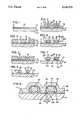
- FIG. 1is a cross-sectional view showing an intermediate stage of fabrication of an integrated circuit, preparatory to metallization in accordance with the invention.
- FIG. 2shows a cross section similar to FIG. 1 following application and patterning of a layer of positive photoresist on the upper surface of the substrate.
- FIG. 3is a view similar to FIG. 2 showing the step of additive metallization to form metal interconnect lines, shown in cross section, along exposed areas of the substrate surface.
- FIG. 4is a view similar to FIG. 3 following removal of the photoresist and intermediate plating layer.
- FIG. 5is a view similar to FIG. 4 following deposition of a dielectric layer over the semiconductor surface and metal interconnect lines.
- FIG. 6is a view similar to FIG. 5 indicating the regions of the dielectric which are removed by an anisotropic etch so as to leave sidewalls along the metal interconnect lines.
- FIG. 7is a view similar to FIG. 6 following isotropic etching of the barrier layer to laterally isolate the interconnect lines electrically from one another.
- FIG. 8is a view similar to FIG. 7 following deposition of dielectric layers over the metal lines and exposed areas of the substrate surface.
- a silicon or other suitable semiconductor substrate 10is processed in conventional manner to form circuit elements (not shown) therein.
- the semiconductor surfaceis passivated with a suitable dielectric, commonly referred to as field oxide.
- a suitable dielectriccommonly referred to as field oxide.
- substrate 10refers to the foregoing general structure.
- a barrier layer 12, such as tungsten or, preferably, titanium tungsten (TiW),is sputter-deposited onto the upper surface 11 of substrate 10 to a thickness of about 1500 angstroms.
- a palladium (Pd) plating layer 14is deposited over layer 12 to the thickness of 100-200 angstroms.
- a layer of photoresist 16is applied over the entire substrate, atop the upper surface 15 of the plating layer 14.
- the photoresistis masked and exposed to form a elongated narrow channel, such as openings 18, wherein the upper surface 15 of the plating layer 14 is exposed.
- a layer of goldis electrodeposited selectively onto the surface of plating layer 14 within openings 18 to a thickness of about 10,000 angstroms.
- This stepforms conductive metal lines 20, 22 with a slightly retrograde sidewall profile (not shown).
- Gold (Au)is preferred for metal interconnect lines in dense, high speed electronic circuits but other metals may be substituted.
- the photoresistis then stripped, exposing surface 15 of plating layer 14, which is then etched in an iodine-based etchant.
- This stepshown in FIG. 4, exposes the surface of the TiW barrier layer 12 as well as sidewalls 24, 26 of the metal lines and sidewalls 14A of the palladium layer.
- the sidewallsare ideally normal to substrate surface 11, as shown in FIG. 4, but are slightly retrograde in practice.
- a semi-conformal dielectric layer 25such as silicon nitride (Si x N y ) is deposited over the entire substrate surface to a thickness of about 4,000 angstroms.
- Layer 25is deposited in contact with the sidewalls 24, 26 and 14A of the metal lines as well as on the upward facing horizontal top surfaces of the metal lines 20, 22 and the exposed upper surface 12A of the barrier layer.
- portions of layer 25are selectively removed to form sidewall spacers 30, 32, as shown in FIG. 6 and 7.
- the portion of layer 25 designated as layer 25A in FIG. 6is removed by an anisotropic etch, herein referred to as the spacer etch.
- anisotropic etchherein referred to as the spacer etch.
- suitable anisotropic etchessuch as, for example, that available in a Tegal 903 reactive ion oxide etcher.
- Sufficient etchingis used to expose the top surfaces of the metal lines 20, 22 and the top surface of the barrier layer 12 in the field areas.
- the field areasare those regions at least 1 ⁇ outside of the edges of the metal lines 24, 26.
- an additional margin of etching 25Breferred to here as an overetch, is used to compensate for nonuniformities of dielectric deposition and anisotropic etch. Without this overetch some portions of the wafer could have dielectric covering areas of the barrier layer 12.
- the preceding etchesleave behind spacers 30, 32 along all the sidewalls of the metal lines 20, 22.
- the spacersserve to protect from subsequent etching an underlying margin of the barrier layer 12 that extends laterally beyond both sidewalls of all of the metal lines.
- the lateral length of this protected marginis principally determined by the deposited thickness of layer 25 (FIG. 5) and, to a lesser extent, by the amount of overetch 25B (FIG. 5A) that is used.
- the barrier layer 12is etched with hydrogen peroxide (H 2 O 2 ) to expose the underlying substrate surface 11 and to laterally isolate the metal interconnect lines electrically from one another.
- the barrier layeris removed from all areas except where it is protected from etching by the presence of the metal lines 20, 22 and the spacers 30, 32 on the sidewalls of the metal lines.
- the remaining areas of barrier metalare identified by reference numeral 12A.
- dielectric layers 36, 38such as silicon nitride and silicon dioxide, are deposited as shown in FIG. 8 to seal the tops of the metal lines.
- the presence of the spacers 30, 32prevents the profile of the gold interconnect lines 20, 22 from deforming during the preheat portion of the deposition cycle.
- the metal linesare completely sealed by the dielectric layers 36 and 38, the barrier layer 12A and the two spacers 30, 32, and are thus prevented from interacting with the substrate.
- the amount of undercut Dwill equal or slightly exceed the thickness of the barrier layer, assuming a slight overetch to assure complete removal of the barrier layer from the substrate surface 11.
- the overetchis in the range of 20-25%.
- a sidewall lateral thickness of about 2,000 angstromsis sufficient to prevent undercutting of the metal lines 20, 22. This thickness is provided by depositing nitride layer 25 to a thickness of about 3,500 angstroms before anisotropic etching to form the sidewall spacers.
Landscapes
- Engineering & Computer Science (AREA)
- Physics & Mathematics (AREA)
- Condensed Matter Physics & Semiconductors (AREA)
- General Physics & Mathematics (AREA)
- Computer Hardware Design (AREA)
- Microelectronics & Electronic Packaging (AREA)
- Power Engineering (AREA)
- Manufacturing & Machinery (AREA)
- Internal Circuitry In Semiconductor Integrated Circuit Devices (AREA)
Abstract
Description
Claims (18)
Priority Applications (1)
| Application Number | Priority Date | Filing Date | Title |
|---|---|---|---|
| US07/562,265US5145571A (en) | 1990-08-03 | 1990-08-03 | Gold interconnect with sidewall-spacers |
Applications Claiming Priority (1)
| Application Number | Priority Date | Filing Date | Title |
|---|---|---|---|
| US07/562,265US5145571A (en) | 1990-08-03 | 1990-08-03 | Gold interconnect with sidewall-spacers |
Publications (1)
| Publication Number | Publication Date |
|---|---|
| US5145571Atrue US5145571A (en) | 1992-09-08 |
Family
ID=24245523
Family Applications (1)
| Application Number | Title | Priority Date | Filing Date |
|---|---|---|---|
| US07/562,265Expired - LifetimeUS5145571A (en) | 1990-08-03 | 1990-08-03 | Gold interconnect with sidewall-spacers |
Country Status (1)
| Country | Link |
|---|---|
| US (1) | US5145571A (en) |
Cited By (17)
| Publication number | Priority date | Publication date | Assignee | Title |
|---|---|---|---|---|
| FR2766616A1 (en)* | 1997-07-26 | 1999-01-29 | Bosch Gmbh Robert | METHOD FOR MANUFACTURING METALLIC MICROSTRUCTURES |
| US5930890A (en)* | 1995-10-12 | 1999-08-03 | Fujitsu Limited | Structure and fabrication procedure for a stable post |
| WO1999040615A1 (en)* | 1998-02-04 | 1999-08-12 | Semitool, Inc. | Method and apparatus for low-temperature annealing of metallization micro-structures in the production of a microelectronic device |
| US6248656B1 (en)* | 1998-08-13 | 2001-06-19 | Tessera, Inc. | Metal-jacketed lead manufacturing process using resist layers |
| US20020022363A1 (en)* | 1998-02-04 | 2002-02-21 | Thomas L. Ritzdorf | Method for filling recessed micro-structures with metallization in the production of a microelectronic device |
| EP1213758A1 (en)* | 2000-12-11 | 2002-06-12 | STMicroelectronics S.r.l. | A method of forming interconnections in semiconductor devices |
| US20060157443A1 (en)* | 2005-01-18 | 2006-07-20 | Ping Mei | Pattern reversal process for self aligned imprint lithography and device |
| US20070273035A1 (en)* | 1998-12-21 | 2007-11-29 | Mou-Shiung Lin | Top layers of metal for high performance IC's |
| US7399713B2 (en) | 1998-03-13 | 2008-07-15 | Semitool, Inc. | Selective treatment of microelectric workpiece surfaces |
| USRE43674E1 (en)* | 2000-10-18 | 2012-09-18 | Megica Corporation | Post passivation metal scheme for high-performance integrated circuit devices |
| CN103681499A (en)* | 2012-09-12 | 2014-03-26 | 中芯国际集成电路制造(上海)有限公司 | Method for manufacturing semiconductor device |
| US20160049483A1 (en)* | 2014-08-15 | 2016-02-18 | Taiwan Semiconductor Manufacturing Company Ltd. | Semiconductor structure and manufacuting method of the same |
| IT201800007967A1 (en)* | 2018-08-08 | 2020-02-08 | St Microelectronics Srl | METHOD OF MANUFACTURING A REDISTRIBUTION LAYER, REDISTRIBUTION LAYER AND INTEGRATED CIRCUIT INCLUDING THE REDISTRIBUTION LAYER |
| IT201800007968A1 (en)* | 2018-08-08 | 2020-02-08 | St Microelectronics Srl | METHOD OF MANUFACTURING A REDISTRIBUTION LAYER, REDISTRIBUTION LAYER AND INTEGRATED CIRCUIT INCLUDING THE REDISTRIBUTION LAYER |
| US10699948B2 (en) | 2017-11-13 | 2020-06-30 | Analog Devices Global Unlimited Company | Plated metallization structures |
| US11469194B2 (en) | 2018-08-08 | 2022-10-11 | Stmicroelectronics S.R.L. | Method of manufacturing a redistribution layer, redistribution layer and integrated circuit including the redistribution layer |
| US12249618B2 (en) | 2022-02-28 | 2025-03-11 | Analog Devices International Unlimited Company | Shaped metal edge for galvanic or capacitive isolator |
Citations (3)
| Publication number | Priority date | Publication date | Assignee | Title |
|---|---|---|---|---|
| US4454014A (en)* | 1980-12-03 | 1984-06-12 | Memorex Corporation | Etched article |
| US4471522A (en)* | 1980-07-08 | 1984-09-18 | International Business Machines Corporation | Self-aligned metal process for field effect transistor integrated circuits using polycrystalline silicon gate electrodes |
| US4687552A (en)* | 1985-12-02 | 1987-08-18 | Tektronix, Inc. | Rhodium capped gold IC metallization |
- 1990
- 1990-08-03USUS07/562,265patent/US5145571A/ennot_activeExpired - Lifetime
Patent Citations (3)
| Publication number | Priority date | Publication date | Assignee | Title |
|---|---|---|---|---|
| US4471522A (en)* | 1980-07-08 | 1984-09-18 | International Business Machines Corporation | Self-aligned metal process for field effect transistor integrated circuits using polycrystalline silicon gate electrodes |
| US4454014A (en)* | 1980-12-03 | 1984-06-12 | Memorex Corporation | Etched article |
| US4687552A (en)* | 1985-12-02 | 1987-08-18 | Tektronix, Inc. | Rhodium capped gold IC metallization |
Cited By (41)
| Publication number | Priority date | Publication date | Assignee | Title |
|---|---|---|---|---|
| US5930890A (en)* | 1995-10-12 | 1999-08-03 | Fujitsu Limited | Structure and fabrication procedure for a stable post |
| FR2766616A1 (en)* | 1997-07-26 | 1999-01-29 | Bosch Gmbh Robert | METHOD FOR MANUFACTURING METALLIC MICROSTRUCTURES |
| US7462269B2 (en) | 1998-02-04 | 2008-12-09 | Semitool, Inc. | Method for low temperature annealing of metallization micro-structures in the production of a microelectronic device |
| US7244677B2 (en) | 1998-02-04 | 2007-07-17 | Semitool. Inc. | Method for filling recessed micro-structures with metallization in the production of a microelectronic device |
| US20020022363A1 (en)* | 1998-02-04 | 2002-02-21 | Thomas L. Ritzdorf | Method for filling recessed micro-structures with metallization in the production of a microelectronic device |
| US20020074233A1 (en)* | 1998-02-04 | 2002-06-20 | Semitool, Inc. | Method and apparatus for low temperature annealing of metallization micro-structures in the production of a microelectronic device |
| US6508920B1 (en) | 1998-02-04 | 2003-01-21 | Semitool, Inc. | Apparatus for low-temperature annealing of metallization microstructures in the production of a microelectronic device |
| US6753251B2 (en) | 1998-02-04 | 2004-06-22 | Semitool, Inc. | Method for filling recessed micro-structures with metallization in the production of a microelectronic device |
| US6806186B2 (en) | 1998-02-04 | 2004-10-19 | Semitool, Inc. | Submicron metallization using electrochemical deposition |
| US7001471B2 (en) | 1998-02-04 | 2006-02-21 | Semitool, Inc. | Method and apparatus for low-temperature annealing of metallization microstructures in the production of a microelectronic device |
| WO1999040615A1 (en)* | 1998-02-04 | 1999-08-12 | Semitool, Inc. | Method and apparatus for low-temperature annealing of metallization micro-structures in the production of a microelectronic device |
| US7144805B2 (en) | 1998-02-04 | 2006-12-05 | Semitool, Inc. | Method of submicron metallization using electrochemical deposition of recesses including a first deposition at a first current density and a second deposition at an increased current density |
| US7399713B2 (en) | 1998-03-13 | 2008-07-15 | Semitool, Inc. | Selective treatment of microelectric workpiece surfaces |
| US6248656B1 (en)* | 1998-08-13 | 2001-06-19 | Tessera, Inc. | Metal-jacketed lead manufacturing process using resist layers |
| US20070273035A1 (en)* | 1998-12-21 | 2007-11-29 | Mou-Shiung Lin | Top layers of metal for high performance IC's |
| US20070284753A1 (en)* | 1998-12-21 | 2007-12-13 | Mou-Shiung Lin | Top layers of metal for high performance IC's |
| US20070284751A1 (en)* | 1998-12-21 | 2007-12-13 | Mou-Shiung Lin | Top layers of metal for high performance IC's |
| US20070284752A1 (en)* | 1998-12-21 | 2007-12-13 | Mou-Shiung Lin | Top layers of metal for high performance IC's |
| US8531038B2 (en) | 1998-12-21 | 2013-09-10 | Megica Corporation | Top layers of metal for high performance IC's |
| US8415800B2 (en) | 1998-12-21 | 2013-04-09 | Megica Corporation | Top layers of metal for high performance IC's |
| US7863654B2 (en) | 1998-12-21 | 2011-01-04 | Megica Corporation | Top layers of metal for high performance IC's |
| US8471384B2 (en) | 1998-12-21 | 2013-06-25 | Megica Corporation | Top layers of metal for high performance IC's |
| US8022545B2 (en) | 1998-12-21 | 2011-09-20 | Megica Corporation | Top layers of metal for high performance IC's |
| US7884479B2 (en) | 1998-12-21 | 2011-02-08 | Megica Corporation | Top layers of metal for high performance IC's |
| US7999384B2 (en) | 1998-12-21 | 2011-08-16 | Megica Corporation | Top layers of metal for high performance IC's |
| USRE43674E1 (en)* | 2000-10-18 | 2012-09-18 | Megica Corporation | Post passivation metal scheme for high-performance integrated circuit devices |
| EP1213758A1 (en)* | 2000-12-11 | 2002-06-12 | STMicroelectronics S.r.l. | A method of forming interconnections in semiconductor devices |
| US6475898B2 (en) | 2000-12-11 | 2002-11-05 | Stmicroelectronics S.R.L. | Method of forming interconnectings in semiconductor devices |
| US20060157443A1 (en)* | 2005-01-18 | 2006-07-20 | Ping Mei | Pattern reversal process for self aligned imprint lithography and device |
| US7585424B2 (en)* | 2005-01-18 | 2009-09-08 | Hewlett-Packard Development Company, L.P. | Pattern reversal process for self aligned imprint lithography and device |
| CN103681499A (en)* | 2012-09-12 | 2014-03-26 | 中芯国际集成电路制造(上海)有限公司 | Method for manufacturing semiconductor device |
| CN103681499B (en)* | 2012-09-12 | 2017-08-01 | 中芯国际集成电路制造(上海)有限公司 | A method of manufacturing a semiconductor device |
| US20160049483A1 (en)* | 2014-08-15 | 2016-02-18 | Taiwan Semiconductor Manufacturing Company Ltd. | Semiconductor structure and manufacuting method of the same |
| US10084060B2 (en)* | 2014-08-15 | 2018-09-25 | Taiwan Semiconductor Manufacturing Company Ltd. | Semiconductor structure and manufacturing method of the same |
| US10699948B2 (en) | 2017-11-13 | 2020-06-30 | Analog Devices Global Unlimited Company | Plated metallization structures |
| US11862518B2 (en) | 2017-11-13 | 2024-01-02 | Analog Devices International Unlimited Company | Plated metallization structures |
| IT201800007967A1 (en)* | 2018-08-08 | 2020-02-08 | St Microelectronics Srl | METHOD OF MANUFACTURING A REDISTRIBUTION LAYER, REDISTRIBUTION LAYER AND INTEGRATED CIRCUIT INCLUDING THE REDISTRIBUTION LAYER |
| IT201800007968A1 (en)* | 2018-08-08 | 2020-02-08 | St Microelectronics Srl | METHOD OF MANUFACTURING A REDISTRIBUTION LAYER, REDISTRIBUTION LAYER AND INTEGRATED CIRCUIT INCLUDING THE REDISTRIBUTION LAYER |
| US11469194B2 (en) | 2018-08-08 | 2022-10-11 | Stmicroelectronics S.R.L. | Method of manufacturing a redistribution layer, redistribution layer and integrated circuit including the redistribution layer |
| US12021046B2 (en) | 2018-08-08 | 2024-06-25 | Stmicroelectronics S.R.L. | Redistribution layer and integrated circuit including redistribution layer |
| US12249618B2 (en) | 2022-02-28 | 2025-03-11 | Analog Devices International Unlimited Company | Shaped metal edge for galvanic or capacitive isolator |
Similar Documents
| Publication | Publication Date | Title |
|---|---|---|
| US5145571A (en) | Gold interconnect with sidewall-spacers | |
| KR100578676B1 (en) | Electroless Copper Deposition Method on Titanium-Containing Surfaces | |
| US4102733A (en) | Two and three mask process for IGFET fabrication | |
| US4714951A (en) | Integrated circuit device which includes a continous layer which consists of conducting portions which are of a silicide of a refractory metal and insulating portions which are of an oxide of the metal | |
| US5387535A (en) | Method of fabricating semiconductor devices in CMOS technology with local interconnects | |
| US4172004A (en) | Method for forming dense dry etched multi-level metallurgy with non-overlapped vias | |
| US4040891A (en) | Etching process utilizing the same positive photoresist layer for two etching steps | |
| EP0540446B1 (en) | Self-aligned contact studs for semiconductor structures | |
| EP0322244A2 (en) | Self-limiting mask undercut process | |
| JPH0391930A (en) | Method of manufacturing semiconductor device | |
| US4977100A (en) | Method of fabricating a MESFET | |
| US4933297A (en) | Method for etching windows having different depths | |
| US4923823A (en) | Method of fabricating a self aligned semiconductor device | |
| JPS6144470A (en) | Method of producing integrated circuit chip | |
| EP0538064A2 (en) | Method of fabricating wiring on a semiconductor substrate using a plating process | |
| US5556797A (en) | Method of fabricating a self-aligned double recess gate profile | |
| JPH0831456B2 (en) | Method for manufacturing semiconductor device | |
| US6194320B1 (en) | Method for preparing a semiconductor device | |
| US4082604A (en) | Semiconductor process | |
| US4400867A (en) | High conductivity metallization for semiconductor integrated circuits | |
| EP0289089B1 (en) | Method of manufacturing a semiconductor device having interconnections located both above a semiconductor region and above an isolation region adjoining it | |
| US5093274A (en) | Semiconductor device and method for manufacture thereof | |
| US5237192A (en) | MESFET semiconductor device having a T-shaped gate electrode | |
| US5620911A (en) | Method for fabricating a metal field effect transistor having a recessed gate | |
| US5136361A (en) | Stratified interconnect structure for integrated circuits |
Legal Events
| Date | Code | Title | Description |
|---|---|---|---|
| AS | Assignment | Owner name:BIPOLAR INTEGRATED TECHNOLOGY, INC., OREGON Free format text:ASSIGNMENT OF ASSIGNORS INTEREST.;ASSIGNORS:LANE, RICHARD H.;EBEL, TIMOTHY M.;REEL/FRAME:005398/0932 Effective date:19900801 | |
| FEPP | Fee payment procedure | Free format text:PAYOR NUMBER ASSIGNED (ORIGINAL EVENT CODE: ASPN); ENTITY STATUS OF PATENT OWNER: LARGE ENTITY | |
| STCF | Information on status: patent grant | Free format text:PATENTED CASE | |
| AS | Assignment | Owner name:OGC SCIENCE PARK LIMITED PARTNERSHIP II DBA SCIEN Free format text:STATUTORY LANDLORD'S LIEN;ASSIGNOR:BIPOLAR INTEGRATED TECHNOLOGY, INC.;REEL/FRAME:006459/0736 Effective date:19911221 | |
| CC | Certificate of correction | ||
| FPAY | Fee payment | Year of fee payment:4 | |
| AS | Assignment | Owner name:MICRON TECHNOLOGY, INC., IDAHO Free format text:ASSIGNMENT OF ASSIGNORS INTEREST;ASSIGNOR:BIT INCORPORATED;REEL/FRAME:007869/0635 Effective date:19960208 Owner name:BIPOLAR INTEGRATED TECHNOLOGY, INC., OREGON Free format text:RELEASE OF SECURITY INTEREST;ASSIGNOR:RAYTHEON COMPANY;REEL/FRAME:007869/0596 Effective date:19960207 Owner name:BIOPOLAR INTEGRATED TECHNOLOGY, INC., OREGON Free format text:RELEASE OF CLAIM OF LIEN UPON CHATTELS;ASSIGNOR:OGC SCIENCE PARK LIMITED PARTNERSHIP II;REEL/FRAME:007869/0594 Effective date:19960201 | |
| REMI | Maintenance fee reminder mailed | ||
| AS | Assignment | Owner name:MICRON TECHNOLOGY, INC., IDAHO Free format text:ASSIGNMENT OF ASSIGNORS INTEREST;ASSIGNOR:BIT INCORPORATED;REEL/FRAME:008753/0993 Effective date:19960408 | |
| FPAY | Fee payment | Year of fee payment:8 | |
| FPAY | Fee payment | Year of fee payment:12 |