US5144191A - Horizontal microelectronic field emission devices - Google Patents
Horizontal microelectronic field emission devicesDownload PDFInfo
- Publication number
- US5144191A US5144191AUS07/714,275US71427591AUS5144191AUS 5144191 AUS5144191 AUS 5144191AUS 71427591 AUS71427591 AUS 71427591AUS 5144191 AUS5144191 AUS 5144191A
- Authority
- US
- United States
- Prior art keywords
- emitter
- electrode
- sidewall
- horizontal
- insulating layer
- Prior art date
- Legal status (The legal status is an assumption and is not a legal conclusion. Google has not performed a legal analysis and makes no representation as to the accuracy of the status listed.)
- Expired - Lifetime
Links
Images


Classifications
- H—ELECTRICITY
- H01—ELECTRIC ELEMENTS
- H01J—ELECTRIC DISCHARGE TUBES OR DISCHARGE LAMPS
- H01J3/00—Details of electron-optical or ion-optical arrangements or of ion traps common to two or more basic types of discharge tubes or lamps
- H01J3/02—Electron guns
- H01J3/021—Electron guns using a field emission, photo emission, or secondary emission electron source
- H01J3/022—Electron guns using a field emission, photo emission, or secondary emission electron source with microengineered cathode, e.g. Spindt-type
Definitions
- This inventionrelates to semiconductor devices and fabrication methods and more particularly to microelectronic field emission devices and methods of fabricating the same.
- Microminiature emittersare well known in the microelectronics art, and are often referred to as "field emitters". These microminiature field emitters are finding widespread use as electron sources in microelectronic devices. For example, field emitters may be used as electron guns. When the electrons are directed to a cathodoluminescent material they may be used for high density display devices. Moreover, the field emitter may be coupled to appropriate microelectronic control electrodes to produce a microelectronic analog to a vacuum tube and thereby produce vacuum integrated circuits.
- a field emittertypically includes a microelectronic field emission electrode.
- the field emission electrodetypically includes a pointed tip, to enhance electron emissions. Conical pointed tips and linear pointed tips are often used.
- An extraction electrodeis typically provided adjacent but not touching the field emission tip, to form an electron emission gap therebetween. Upon application of an appropriate voltage between the field emission electrode and the extraction electrode, quantum mechanical tunneling or other known phenomena cause the tip to emit an electron beam.
- an array of field emission tipsmay be formed on the horizontal face of a substrate such as a silicon semiconductor substrate. Extraction electrodes and other electrodes as necessary may also be provided on the substrate. Support circuitry may also be fabricated on or in the substrate, using well known microelectronic techniques.
- Field emittersmay be classified as either “vertical” field emitters or “horizontal” field emitters, depending upon the orientation of the emitted electron beam relative to the horizontal substrate face.
- a vertical field emitterone or more emitter tips are formed on the horizontal face of a substrate to emit electrons vertically, i.e. perpendicular to the face of the substrate.
- a plurality of horizontal electrode layersmay be formed on, and generally parallel to, the substrate face, to provide extraction electrodes and other control electrodes as necessary.
- Such vertical field emittersare described in U.S. Pat. No. 4,008,412 to Yuito et al.; U.S. Pat. No. 4,163,949 to Shelton; U.S. Pat. No.
- the second class of emittersis generally referred to as "horizontal" emitters.
- Horizontal emittersemit a beam of electrons generally parallel to the horizontal face of the substrate on which they are formed.
- these emittersare formed by fabricating discrete horizontal emitters and horizontal electrodes in a single horizontal layer parallel to the horizontal face of the semiconductor substrate.
- horizontal emitters, horizontal extraction electrodes and horizontal collector or other electrodesare formed. See for example U.S. Pat. No. 4,728,851 to Lambe and U.S. Pat. No. 4,827,177 to Lee et al.
- horizontal field emittershave also been difficult to manufacture and have been limited in power handling capacity and speed.
- manufacture of a horizontal field emitterhas required the formation of discrete horizontal microelectronic structures in a single horizontal layer on a substrate. It has been difficult to fabricate these small, discrete horizontal structures with a small spacing therebetween.
- the emitter and electrode layershave typically been formed of thin film, closely spaced metallization layers, thereby limiting power handling capacity and device speed.
- a horizontal microelectronic field emitterwhich includes a electrode, on the horizontal face of a substrate. An end of the horizontal emitter electrode and an end of the vertical extraction electrode form an electron emission gap therebetween.
- the emitter electrodeis formed on an insulating layer on the face of a substrate.
- the insulating layeralso includes a sidewall, and the extraction electrode is formed on the sidewall with one end thereof extending adjacent one end of the emitter electrode. The one end of the emitter electrode and the one end of the extraction electrode form an electron emission gap therebetween.
- the emitter electrode of the present inventionis horizontal, it may be formed of thick layers of high conductivity metal surrounding a very thin emitter tip metal, so that high power handling may be provided, with low resistivity.
- the vertical extraction electrodeis formed on the sidewall of the insulating layer, a small electron emission gap may be obtained, with the gap size being determined by thin film deposition techniques rather than by lithography. High fields may thereby be obtained, at reasonable extraction currents and at moderate voltages.
- the extraction electrode and emitter electrodeare generally perpendicular to one another, the insulating layer may be relatively thick, thereby decreasing the capacitive coupling between the emitter and extraction electrodes to thereby provide a high speed device.
- the field emitter of the present inventionmay be formed in a number of configurations depending on the specific application involved.
- a second insulating layermay be formed on the substrate face, with the second insulating layer also having a sidewall, spaced from the first sidewall, to define a cavity.
- a collector electrodemay be formed on the sidewall of the second insulating layer, so that vertical extractor and collector electrodes may be provided for the horizontal emitter electrode.
- a capmay be formed on the first and second insulating layers, bridging the cavity, to encapsulate the cavity.
- the cavitymay be evacuated or filled with gas.
- the field emitter device of the present inventionmay be cylindrical, in which case the first insulating layer is a cylindrical insulating layer with a cylindrical first sidewall.
- the emitter electrodeis a circular (i.e. ring or disk shaped) emitter electrode on the top surface of the cylindrical sidewall
- the extraction electrodeis a cylindrical extraction electrode on the first sidewall.
- a circular electron emission gapis thereby formed, with electrons emitted radially outward from the circular emitter.
- a second insulating layermay be formed surrounding the first insulator, and having a second cylindrical sidewall concentric with the first cylindrical sidewall.
- a cylindrical collector electrodemay be formed on the second sidewall.
- a ring-shaped emittermay emit electrons radially inward, towards vertical, cylindrical, extractor and collector electrodes.
- the field emitter of the present inventionmay also be planar, as opposed to cylindrical.
- the first insulating layermay have a planar sidewall, with the emitter electrode being a planar horizontal electrode on the insulating layer, and the extraction electrode being a planar vertical electrode on the sidewall, to thereby form an elongated electron emission gap.
- a second insulating layermay be formed on the substrate.
- the second insulating layerincludes a second planar sidewall spaced from and parallel to the first planar sidewall, and a vertical collector electrode may be formed on the second planar sidewall. It will also be understood by those having skill in the art that shapes other than cylindrical and planar may be used for particular device applications.
- a plurality of horizontal emitter electrodesmay be vertically stacked on one another between one or more insulating layers.
- a single vertical extraction electrode or a plurality of extraction electrodesmay be formed on the resultant insulating layer sidewalls.
- one or more collector electrodesmay be formed.
- a collector electrodemay also be located on the face of the substrate adjacent the first sidewall, rather than, or in addition to, being located on a second sidewall spaced from the first sidewall.
- the collector electrodemay be a light emissive material or an x-ray emissive material, to form a light or x-ray source.
- the field emitter of the present inventionmay also include a metal layer, parallel to and spaced from an emitter electrode by an intervening insulating layer.
- the emitter electrode and the metal layerform a capacitive emitter structure.
- Chargemay be injected onto the capacitive emitter using a second emitter located opposite the capacitive emitter.
- a high speed, radiation hardened Dynamic Random Access Memory (DRAM) cellis thereby formed.
- a predetermined chargemay be stored on the capacitive emitter in a write operation, and stored charge may be sensed in a read operation.
- the DRAM cellmust be refreshed periodically, to restore charge that has leaked from the capacitive emitter.
- the field emitter of the present inventionmay also be coupled to a feedback capacitor to produce an oscillator.
- a programmable piezoelectric capacitorhaving a dielectric made from, for example, sol gel lead zirconate titanate, may also be produced.
- the shape of the emitted frequency bandsmay be varied, or multiple frequency oscillators may be produced. Such multiple frequency oscillators may be used to create a carrier frequency with signal overlay, or a multistate memory.
- the field emitter of the present inventionmay be fabricated by forming an insulating layer on the face of a substrate. An emitter electrode is formed on the insulating layer. A portion of the insulating layer is then removed to form a first sidewall. An extraction electrode is then formed on the first sidewall.
- a plurality of emitter electrodes and insulating layersmay be formed. A portion of the multiple emitter electrodes and insulating layers may then be etched to the substrate face, to form the first sidewall. The first sidewall may then be metallized to form the extraction electrodes. The etching process may also form the second sidewall, spaced from the first sidewall. The second sidewall may be metallized, simultaneous with the extraction electrode, to form the collector electrode.
- a horizontal emitter having a vertical extractor electrodemay thereby be formed using well known microelectronic techniques.
- FIG. 1illustrates a simplified cross-sectional view of a microelectronic field emitter according to the present invention.
- FIG. 3illustrates a perspective view of a planar microelectronic field emitter having multiple emitters on a sidewall according to the present invention.
- FIG. 4illustrates a perspective view of a field emitter having multiple emitters on a pair of sidewalls and a collector on the substrate face, according to the present invention.
- FIG. 6illustrates a perspective view of one quadrant of a first embodiment of cylindrical field emitter according to the present invention.
- FIG. 7illustrates a perspective view of one quadrant of a second embodiment of cylindrical field emitter according to the present invention.
- FIGS. 8A-8Jschematically illustrate cross-sectional views of a sequence of steps for fabricating a field emitter of the present invention.
- FIG. 9illustrates a perspective view of the field emitter device of FIG. 8J.
- FIG. 10illustrates a cross sectional view of a field emitter having a charge storing emitter electrode according to the present invention.
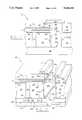
- Emitter electrode 12may be formed of thick layers 16 of high conductivity metal surrounding a thin emitter tip 14. Also shown in FIG. 1 are optional insulating layers 84 and 86, formed immediately above and below emitter electrode 12. Insulating layers 84 and 86 may be used to define the distance between extraction electrode 18 and the emitter tip 14 to make certain the electrodes do not touch, and a small, well defined electron emission gap 22 is formed.
- emitter connector 32electrically connects emitter 12 to substrate 28.
- Substrate 28may include external electrical connections for emitter electrode 12, extractor electrode 18 and collector electrode 24 (not shown), as will be described in detail below.
- Substrate 28may also include other microelectronic circuitry, not shown.
- Optional cap 34may be formed on second and third insulating layers 30 and 38, respectively. Cap 34 encapsulates cavity 36 in the microelectronic emitter to form a vacuum microelectronic integrated circuit structure. Other gases may also be encapsulated in cavity 36 for various applications. For example, hydrogen may be used to minimize chemical degradation of the emitter.
- the horizontal emitter electrode 12is sandwiched between thick dielectric layers 20 and 38, to thereby form a high speed device with reduced parasitic capacitance.
- the emitter electrode 12may be fabricated using thick emitter layers 16 and a thin emitter tip 14, thereby providing a low resistivity emitter.
- the extraction electrode 18may be separated from the emitter by thick dielectric layers 20 and 38, thereby further reducing stray capacitance.
- a small extraction electrode to emitter gap 22may be provided so that a high electric field and a large extracted current may be obtained at moderate extraction voltages. Accordingly, a high speed, high efficiency device may be fabricated.
- a variety of field emitter structuresmay be provided according to the present invention, to suit a variety of applications.
- a number of sample structureswill now be described.
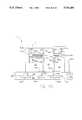
- field emitter 40includes a planar vertical extraction electrode 18a and a planar horizontal emitter electrode 12, to thereby form an elongated electron emission gap 22 therebetween.
- Extraction electrode 18ais formed on sidewall 20a of first insulating layer 20, and emitter either directly, or with optional insulating layer 86.
- a collector electrode 24may be formed on the sidewall 30a of second insulating layer 30.
- a third insulating layer 38may be formed on emitter 12, with an extraction electrode 18b formed on the sidewall 38a thereof.
- Optional insulating layer 84may also be formed.
- a top extractor electrode contact 62 and a top collector electrode contact 64may be used, together with or instead of bottom contacts 58 and 60, to electrically contact the extractor electrode 18b and collector electrode 24 respectively.
- layers 62 and 64may be formed as insulating layers, or these layers may be omitted.
- a cap(not shown in FIG. 2) may be provided on layers 62 and 64, bridging cavity 36, in order to allow evacuation of cavity 36 or filling of cavity 36 with an appropriate gas.
- FIG. 3a planar, multiple emitter structure 70 according to the invention is shown.
- a plurality of emitter electrodes 12a and 12bare connected to a common emitter connector 32 via backside connections.
- a plurality of extraction electrodes 18a-18cmay be individually or collectively controlled.
- the field emitter structure 70 of FIG. 3includes a single collector electrode 24. However, it will be understood by those having skill in the art that a plurality of collector electrodes may also be formed, and may be individually controlled.
- the multiple emitter structure 70 of FIG. 3may be used as a transistor which can produce current flow in either direction by simply changing the bias conditions. Moreover, by operating the multiple emitters in parallel, a source of high intensity electrons may be obtained. It will be understood by those having skill in the art that because microelectronic techniques allow emitter electrodes 12a and 12b to be precisely spaced from and aligned to one another, opposing, highly aligned electron beam sources may be produced. High intensity magnetic fields (not shown) may also be used to confine electrons in the cavity 36.
- a cap 34(not shown in FIG. 3) may be provided, which may have a mirrored bottom surface to create resonance of light beams and thereby create a coherent laser light source.
- FIGS. 2-5use planar emitters, extractors and collectors. It will be understood by those having skill in the art that a variety of nonplanar emitters, extractors and collectors may also be used. Referring now to FIGS. 6 and 7, an example of cylindrical field emitters will now be described. For ease of illustration, only one quadrant of the field emitter is shown. In general, reference numbers used in FIGS. 2-5 will be used, except prime (') notation will be used to indicate cylindrical or circular parts, as opposed to the planar parts.
- FIGS. 8A-8Ja sequence of steps for forming the planar emitter of FIG. 2 will be described. It will be understood by those having skill in the art that the sequence of steps described in connection with FIGS. 8A-8J may be modified to form the emitters described in FIGS. 3-7.
- first insulating layer 20is formed on substrate 28.
- Insulating layer 20may be formed of chemical vapor deposited silicon dioxide or may be preferably formed by spin coating polyimide. Insulating layer 20 is preferably fairly thick, on the order of 10 ⁇ m. As shown in FIG. 8B, insulator 20 tends to conformally deposit so that ridges are formed above pads 56, 58, and 60.
- Optional insulating layer 86is then formed on insulating layer 20. Insulating layer 86 is preferably 0.1 ⁇ m of silicon dioxide. However, silicon nitride may also be used. As shown, insulating layer 86 is conformally formed on insulating layer 20. It will be understood by those having skill in the art that insulator 86 is preferably differential etching material with insulator 20.
- the emitter connector 32is formed.
- a number of well known techniquesmay be used to form emitter connector 32.
- insulating layers 20 and 86may be patterned and etched, and then a conductor may be deposited therein.
- the conductormay be deposited using selective chemical vapor deposition of tungsten.
- evaporation or blanket deposition and etch techniquesmay also be used.
- nickelmay be electrodelessly deposited in the etched portion of insulator 20.
- the emitter electrode 12is formed.
- the thin emitter tip 14is formed between thick emitter layers 16.
- thick emitter layers 16are 0.4 ⁇ m thick layers of aluminum, and emitter tip 14 is a 0.01 ⁇ m thick layer of tungsten.
- chromium/copper layersmay also be used instead of aluminum.
- optional insulating layer 84is formed on upper thick emitter layer 16. Insulating layer 84 is preferably 0.1 ⁇ m of silicon dioxide, although silicon nitride may also be used.
- layers 86, 16, 14 and 84are etched to form the emitter 12 shown in FIG. 8D. It will be understood by those having skill in the art that lift-off techniques may also be used to form emitter electrode 12. It will also be understood by those having skill in the art that insulating layers 84 and 86 are optional, and may be used to define the distance between the extraction electrode 18 (formed in FIG. 8I) and the emitter tip 14 to make certain that the electrodes do not touch and a small, well defined electron emission gap is formed.
- emitter electrode 12need not be patterned at this point in the sequence of operations. Rather, the emitter 12 may be left unpatterned and may be patterned later, when cavity 36 is formed, as part of the processing of FIG. 8G.
- an optional sidewall spacer 88is formed around emitter 12, using well known photolithographic techniques.
- the sidewall spaceris preferably 0.2 ⁇ m silicon dioxide or silicon nitride.
- the sidewall spaceris used to protect the metal layers of emitter electrode 12 during subsequent fabrication steps.
- insulating layer 38is formed on the emitter structure.
- insulating layer 38is spun-on polyimide about 1 ⁇ m thick, although chemical vapor deposited silicon dioxide may also be used.
- insulating layer 84is preferably differential etching material with insulating layer 38. If conductors 62 and 64 will be used in the particular application, they may be photolithographically defined as shown. If conductors are not required, insulating layers 62 and 64 may nonetheless be formed, for use in defining the subsequent etch. If conductors are used, they are preferably 0.5 ⁇ m aluminum with optional TiN or Mo coatings. If insulators are used, 0.5 ⁇ m of silicon nitride is preferably used.
- cavity 36is formed by directionally etching insulating layers 20 and 38 using layers 62 and 64 as a mask. Accordingly, the emitter and extractor electrodes may be self-aligned.
- a suitable dry etchwhich can directionally etch insulator 38, insulator 20 and metal emitter electrode 12 is buffered HF in ethylene glycol.
- the sidewalls 20a, 30a and 38amay be etched back using oxygen plasma to etch back polyimide, or dilute hydrofluoric acid to etch back silicon dioxide, to cause the end of emitter 12 to protrude into cavity 36 as shown in FIG. 8G.
- the collector and extractor electrodesare formed by conformally depositing a conductor over the entire exposed surface.
- conductor 78may be conformally deposited using chemical vapor deposition.
- Conductor 78is preferably tungsten, 1.0 ⁇ m thick, although highly doped polysilicon or other known conductors may be used. It will be understood by those having skill in the art that an adhesion layer may be used to ensure adhesion of conformal conductor layer 78 to the underlying material.
- an anisotropic (directional) etchis performed on conformal conductor 78.
- conductor 78is tungsten
- a reactive ion etch in sulfur hexafluoridemay be performed.
- the directional etchsubstantially etches the horizontal surfaces of conformal conductor 78, but does not substantially etch the vertical surfaces of conductor 78.
- vertical extraction electrodes 18a, 18b and collector electrode 24are formed.
- the remaining vertical portions 82 of conformal conductor 78may be removed, or they may remain as shown.
- a wet etch of insulating layers 84 and 86may be performed.
- the thin emitter tip 14may be etched back to its desired position and the top and bottom emitter metals 16 may also be etched in order to form a sharp edge as shown in FIG. 8J.
- FIG. 9illustrates the completed structure of FIG. 8H in perspective.
- Cylindrical, ring-shaped and other nonplanar emittersmay be formed using a similar sequence of steps including patterning the desired shape.
- multiple emitters, extractors and/or collectorsmay be formed by repeating at least some of the illustrated steps.
- field emitter 110includes an emitter electrode 129 having a pair of metal plate layers 112a, 112b parallel thereto and spaced therefrom by insulating layers 86a and 84a, respectively.
- connector 32amay be used to electrically connect metal plates 112a and 112b.
- metal plates 112a and 112bmay be directly connected to one another without using connector 32a.
- emitter 12a and metal plate layers 112are electrically floating, i.e. they are insulated from one another and from the other elements of field emitter 110. Accordingly, charge placed on emitter electrode 12a will be capacitively stored between emitter electrode 12a and plates 112, limited only by charge leakage.
- Field emitter 110may form a cell of a DRAM, with a binary ONE or ZERO being indicated by the presence or absence of charge On emitter electrode 12a.
- chargemay be placed on emitter electrode 12a by emitter electrode 12b, which is coplanar to emitter electrode 12a and spaced therefrom across cavity 36.
- Datamay be read or sensed using extractor electrodes 18a and 18b to extract charge from emitter electrode 12a, if present, and using emitter electrode 12b and/or extractors 18c and 18d to sense the extracted charge, if any.
- Field emitter 110may be fabricated as described above in FIG. 9, with the additional steps of fabricating plate 112a on first insulating layer 20 before fabricating emitter 12a, and fabricating plate 112b on emitter 12a thereafter. A high speed, radiation hardened DRAM cell may thereby be formed.
Landscapes
- Cold Cathode And The Manufacture (AREA)
Abstract
Description
Claims (28)
Priority Applications (1)
| Application Number | Priority Date | Filing Date | Title |
|---|---|---|---|
| US07/714,275US5144191A (en) | 1991-06-12 | 1991-06-12 | Horizontal microelectronic field emission devices |
Applications Claiming Priority (1)
| Application Number | Priority Date | Filing Date | Title |
|---|---|---|---|
| US07/714,275US5144191A (en) | 1991-06-12 | 1991-06-12 | Horizontal microelectronic field emission devices |
Publications (1)
| Publication Number | Publication Date |
|---|---|
| US5144191Atrue US5144191A (en) | 1992-09-01 |
Family
ID=24869387
Family Applications (1)
| Application Number | Title | Priority Date | Filing Date |
|---|---|---|---|
| US07/714,275Expired - LifetimeUS5144191A (en) | 1991-06-12 | 1991-06-12 | Horizontal microelectronic field emission devices |
Country Status (1)
| Country | Link |
|---|---|
| US (1) | US5144191A (en) |
Cited By (72)
| Publication number | Priority date | Publication date | Assignee | Title |
|---|---|---|---|---|
| US5272411A (en)* | 1992-01-28 | 1993-12-21 | Itt Corporation | Coaxial triode apparatus |
| US5289077A (en)* | 1991-01-28 | 1994-02-22 | Sony Corporation | Microelectronic ballistic transistor |
| US5312777A (en)* | 1992-09-25 | 1994-05-17 | International Business Machines Corporation | Fabrication methods for bidirectional field emission devices and storage structures |
| US5343110A (en)* | 1991-06-04 | 1994-08-30 | Matsushita Electric Industrial Co., Ltd. | Electron emission element |
| US5384509A (en)* | 1991-07-18 | 1995-01-24 | Motorola, Inc. | Field emission device with horizontal emitter |
| US5502348A (en)* | 1993-12-20 | 1996-03-26 | Motorola, Inc. | Ballistic charge transport device with integral active contaminant absorption means |
| US5580467A (en)* | 1995-03-29 | 1996-12-03 | Samsung Display Devices Co., Ltd. | Method of fabricating a field emission micro-tip |
| WO1996038854A1 (en)* | 1995-06-02 | 1996-12-05 | Advanced Vision Technologies, Inc. | Lateral-emitter field-emission device with simplified anode and fabrication thereof |
| WO1996042113A1 (en)* | 1995-06-13 | 1996-12-27 | Advanced Vision Technologies, Inc. | Laminar composite lateral field-emission cathode and fabrication process |
| WO1997002586A1 (en)* | 1995-07-05 | 1997-01-23 | Advanced Vision Technologies, Inc. | Direct electron injection field-emission display device and fabrication process |
| US5600200A (en) | 1992-03-16 | 1997-02-04 | Microelectronics And Computer Technology Corporation | Wire-mesh cathode |
| US5601966A (en) | 1993-11-04 | 1997-02-11 | Microelectronics And Computer Technology Corporation | Methods for fabricating flat panel display systems and components |
| WO1997009733A1 (en)* | 1995-09-06 | 1997-03-13 | Advanced Vision Technologies, Inc. | High-frequency field-emission device and fabrication process |
| US5612712A (en) | 1992-03-16 | 1997-03-18 | Microelectronics And Computer Technology Corporation | Diode structure flat panel display |
| US5616061A (en)* | 1995-07-05 | 1997-04-01 | Advanced Vision Technologies, Inc. | Fabrication process for direct electron injection field-emission display device |
| US5618216A (en)* | 1995-06-02 | 1997-04-08 | Advanced Vision Technologies, Inc. | Fabrication process for lateral-emitter field-emission device with simplified anode |
| US5628663A (en)* | 1995-09-06 | 1997-05-13 | Advanced Vision Technologies, Inc. | Fabrication process for high-frequency field-emission device |
| US5629580A (en)* | 1994-10-28 | 1997-05-13 | International Business Machines Corporation | Lateral field emission devices for display elements and methods of fabrication |
| US5644190A (en)* | 1995-07-05 | 1997-07-01 | Advanced Vision Technologies, Inc. | Direct electron injection field-emission display device |
| US5647998A (en)* | 1995-06-13 | 1997-07-15 | Advanced Vision Technologies, Inc. | Fabrication process for laminar composite lateral field-emission cathode |
| US5651712A (en)* | 1994-09-18 | 1997-07-29 | International Business Machines Corporation | Multi-chromic lateral field emission devices with associated displays and methods of fabrication |
| US5666019A (en)* | 1995-09-06 | 1997-09-09 | Advanced Vision Technologies, Inc. | High-frequency field-emission device |
| US5669802A (en)* | 1995-10-30 | 1997-09-23 | Advanced Vision Technologies, Inc. | Fabrication process for dual carrier display device |
| US5675216A (en) | 1992-03-16 | 1997-10-07 | Microelectronics And Computer Technololgy Corp. | Amorphic diamond film flat field emission cathode |
| US5679043A (en) | 1992-03-16 | 1997-10-21 | Microelectronics And Computer Technology Corporation | Method of making a field emitter |
| US5684356A (en)* | 1996-03-29 | 1997-11-04 | Texas Instruments Incorporated | Hydrogen-rich, low dielectric constant gate insulator for field emission device |
| US5688158A (en)* | 1995-08-24 | 1997-11-18 | Fed Corporation | Planarizing process for field emitter displays and other electron source applications |
| US5703380A (en)* | 1995-06-13 | 1997-12-30 | Advanced Vision Technologies Inc. | Laminar composite lateral field-emission cathode |
| US5763997A (en) | 1992-03-16 | 1998-06-09 | Si Diamond Technology, Inc. | Field emission display device |
| EP0848406A3 (en)* | 1996-12-13 | 1998-08-12 | Motorola, Inc. | Method for fabricating a field emission device having reduced row-to-column leakage |
| US5811929A (en)* | 1995-06-02 | 1998-09-22 | Advanced Vision Technologies, Inc. | Lateral-emitter field-emission device with simplified anode |
| US5828288A (en)* | 1995-08-24 | 1998-10-27 | Fed Corporation | Pedestal edge emitter and non-linear current limiters for field emitter displays and other electron source applications |
| US5828163A (en)* | 1997-01-13 | 1998-10-27 | Fed Corporation | Field emitter device with a current limiter structure |
| US5831384A (en)* | 1995-10-30 | 1998-11-03 | Advanced Vision Technologies, Inc. | Dual carrier display device |
| WO1998032145A3 (en)* | 1996-12-30 | 1998-11-19 | Advanced Vision Tech Inc | Surface electron display device and fabrication process |
| US5844351A (en)* | 1995-08-24 | 1998-12-01 | Fed Corporation | Field emitter device, and veil process for THR fabrication thereof |
| US5861707A (en) | 1991-11-07 | 1999-01-19 | Si Diamond Technology, Inc. | Field emitter with wide band gap emission areas and method of using |
| US5872421A (en)* | 1996-12-30 | 1999-02-16 | Advanced Vision Technologies, Inc. | Surface electron display device with electron sink |
| US5907215A (en)* | 1996-04-18 | 1999-05-25 | Pixtech S.A. | Flat display screen with hydrogen source |
| US5920148A (en)* | 1995-05-08 | 1999-07-06 | Advanced Vision Technologies, Inc. | Field emission display cell structure |
| US5965971A (en)* | 1993-01-19 | 1999-10-12 | Kypwee Display Corporation | Edge emitter display device |
| US6015324A (en)* | 1996-12-30 | 2000-01-18 | Advanced Vision Technologies, Inc. | Fabrication process for surface electron display device with electron sink |
| US6127773A (en) | 1992-03-16 | 2000-10-03 | Si Diamond Technology, Inc. | Amorphic diamond film flat field emission cathode |
| US6404113B1 (en)* | 1999-01-21 | 2002-06-11 | Nec Corporation | Field emission type cold cathode element, method of fabricating the same, and display device |
| US6629869B1 (en) | 1992-03-16 | 2003-10-07 | Si Diamond Technology, Inc. | Method of making flat panel displays having diamond thin film cathode |
| US20040227212A1 (en)* | 2001-08-31 | 2004-11-18 | Klaus Goller | Making contact with the emitter contact of a semiconductor |
| US20050057178A1 (en)* | 2003-09-11 | 2005-03-17 | Tomio Yaguchi | Flat panel display device |
| EP1016113A4 (en)* | 1997-09-17 | 2005-08-17 | Candescent Intellectual Prop | Dual-layer metal for flat panel display |
| US20050242705A1 (en)* | 2004-04-29 | 2005-11-03 | You-Jong Kim | Electron emission device |
| US20070053495A1 (en)* | 2003-04-25 | 2007-03-08 | Morton Edward J | X-ray tube electron sources |
| US7684538B2 (en) | 2003-04-25 | 2010-03-23 | Rapiscan Systems, Inc. | X-ray scanning system |
| US20100289399A1 (en)* | 2009-05-14 | 2010-11-18 | Canon Kabushiki Kaisha | Electron beam apparatus and image display apparatus using the same |
| US7949101B2 (en) | 2005-12-16 | 2011-05-24 | Rapiscan Systems, Inc. | X-ray scanners and X-ray sources therefor |
| US8135110B2 (en) | 2005-12-16 | 2012-03-13 | Rapiscan Systems, Inc. | X-ray tomography inspection systems |
| US8451974B2 (en) | 2003-04-25 | 2013-05-28 | Rapiscan Systems, Inc. | X-ray tomographic inspection system for the identification of specific target items |
| US8837669B2 (en) | 2003-04-25 | 2014-09-16 | Rapiscan Systems, Inc. | X-ray scanning system |
| US9020095B2 (en) | 2003-04-25 | 2015-04-28 | Rapiscan Systems, Inc. | X-ray scanners |
| US9052403B2 (en) | 2002-07-23 | 2015-06-09 | Rapiscan Systems, Inc. | Compact mobile cargo scanning system |
| US9113839B2 (en) | 2003-04-25 | 2015-08-25 | Rapiscon Systems, Inc. | X-ray inspection system and method |
| US9218933B2 (en) | 2011-06-09 | 2015-12-22 | Rapidscan Systems, Inc. | Low-dose radiographic imaging system |
| US9223052B2 (en) | 2008-02-28 | 2015-12-29 | Rapiscan Systems, Inc. | Scanning systems |
| US9223050B2 (en) | 2005-04-15 | 2015-12-29 | Rapiscan Systems, Inc. | X-ray imaging system having improved mobility |
| US9223049B2 (en) | 2002-07-23 | 2015-12-29 | Rapiscan Systems, Inc. | Cargo scanning system with boom structure |
| US9285498B2 (en) | 2003-06-20 | 2016-03-15 | Rapiscan Systems, Inc. | Relocatable X-ray imaging system and method for inspecting commercial vehicles and cargo containers |
| US9332624B2 (en) | 2008-05-20 | 2016-05-03 | Rapiscan Systems, Inc. | Gantry scanner systems |
| US9420677B2 (en) | 2009-01-28 | 2016-08-16 | Rapiscan Systems, Inc. | X-ray tube electron sources |
| US9429530B2 (en) | 2008-02-28 | 2016-08-30 | Rapiscan Systems, Inc. | Scanning systems |
| US9726619B2 (en) | 2005-10-25 | 2017-08-08 | Rapiscan Systems, Inc. | Optimization of the source firing pattern for X-ray scanning systems |
| US9791590B2 (en) | 2013-01-31 | 2017-10-17 | Rapiscan Systems, Inc. | Portable security inspection system |
| US10483077B2 (en) | 2003-04-25 | 2019-11-19 | Rapiscan Systems, Inc. | X-ray sources having reduced electron scattering |
| US10591424B2 (en) | 2003-04-25 | 2020-03-17 | Rapiscan Systems, Inc. | X-ray tomographic inspection systems for the identification of specific target items |
| CN111093502A (en)* | 2017-07-26 | 2020-05-01 | 深圳帧观德芯科技有限公司 | Integrated X-ray source |
Citations (16)
| Publication number | Priority date | Publication date | Assignee | Title |
|---|---|---|---|---|
| US3982147A (en)* | 1975-03-07 | 1976-09-21 | Charles Redman | Electric device for processing signals in three dimensions |
| US4008412A (en)* | 1974-08-16 | 1977-02-15 | Hitachi, Ltd. | Thin-film field-emission electron source and a method for manufacturing the same |
| US4163949A (en)* | 1977-12-27 | 1979-08-07 | Joe Shelton | Tubistor |
| US4325084A (en)* | 1978-01-27 | 1982-04-13 | U.S. Philips Corporation | Semiconductor device and method of manufacturing same, as well as a pick-up device and a display device having such a semiconductor device |
| US4574216A (en)* | 1981-10-29 | 1986-03-04 | U.S. Philips Corporation | Cathode-ray tube and semiconductor device for use in such a cathode-ray tube |
| US4578614A (en)* | 1982-07-23 | 1986-03-25 | The United States Of America As Represented By The Secretary Of The Navy | Ultra-fast field emitter array vacuum integrated circuit switching device |
| US4663559A (en)* | 1982-09-17 | 1987-05-05 | Christensen Alton O | Field emission device |
| US4721885A (en)* | 1987-02-11 | 1988-01-26 | Sri International | Very high speed integrated microelectronic tubes |
| US4728851A (en)* | 1982-01-08 | 1988-03-01 | Ford Motor Company | Field emitter device with gated memory |
| JPS6433833A (en)* | 1987-07-29 | 1989-02-03 | Canon Kk | Electron emitting element |
| US4827177A (en)* | 1986-09-08 | 1989-05-02 | The General Electric Company, P.L.C. | Field emission vacuum devices |
| US4835438A (en)* | 1986-11-27 | 1989-05-30 | Commissariat A L'energie Atomique | Source of spin polarized electrons using an emissive micropoint cathode |
| US4916356A (en)* | 1988-09-26 | 1990-04-10 | The United States Of America As Represented By The Secretary Of The Air Force | High emissivity cold cathode ultrastructure |
| US4940916A (en)* | 1987-11-06 | 1990-07-10 | Commissariat A L'energie Atomique | Electron source with micropoint emissive cathodes and display means by cathodoluminescence excited by field emission using said source |
| US4956574A (en)* | 1989-08-08 | 1990-09-11 | Motorola, Inc. | Switched anode field emission device |
| US5053673A (en)* | 1988-10-17 | 1991-10-01 | Matsushita Electric Industrial Co., Ltd. | Field emission cathodes and method of manufacture thereof |
- 1991
- 1991-06-12USUS07/714,275patent/US5144191A/ennot_activeExpired - Lifetime
Patent Citations (18)
| Publication number | Priority date | Publication date | Assignee | Title |
|---|---|---|---|---|
| US4008412A (en)* | 1974-08-16 | 1977-02-15 | Hitachi, Ltd. | Thin-film field-emission electron source and a method for manufacturing the same |
| US3982147A (en)* | 1975-03-07 | 1976-09-21 | Charles Redman | Electric device for processing signals in three dimensions |
| US4163949A (en)* | 1977-12-27 | 1979-08-07 | Joe Shelton | Tubistor |
| US4325084A (en)* | 1978-01-27 | 1982-04-13 | U.S. Philips Corporation | Semiconductor device and method of manufacturing same, as well as a pick-up device and a display device having such a semiconductor device |
| US4554564A (en)* | 1978-01-27 | 1985-11-19 | U.S. Philips Corporation | Semiconductor device and method of manufacturing same, as well as a pick-up device and a display device having such a semiconductor device |
| US4574216A (en)* | 1981-10-29 | 1986-03-04 | U.S. Philips Corporation | Cathode-ray tube and semiconductor device for use in such a cathode-ray tube |
| US4728851A (en)* | 1982-01-08 | 1988-03-01 | Ford Motor Company | Field emitter device with gated memory |
| US4578614A (en)* | 1982-07-23 | 1986-03-25 | The United States Of America As Represented By The Secretary Of The Navy | Ultra-fast field emitter array vacuum integrated circuit switching device |
| US4663559A (en)* | 1982-09-17 | 1987-05-05 | Christensen Alton O | Field emission device |
| US4827177A (en)* | 1986-09-08 | 1989-05-02 | The General Electric Company, P.L.C. | Field emission vacuum devices |
| US4835438A (en)* | 1986-11-27 | 1989-05-30 | Commissariat A L'energie Atomique | Source of spin polarized electrons using an emissive micropoint cathode |
| US4721885A (en)* | 1987-02-11 | 1988-01-26 | Sri International | Very high speed integrated microelectronic tubes |
| JPS6433833A (en)* | 1987-07-29 | 1989-02-03 | Canon Kk | Electron emitting element |
| US4940916A (en)* | 1987-11-06 | 1990-07-10 | Commissariat A L'energie Atomique | Electron source with micropoint emissive cathodes and display means by cathodoluminescence excited by field emission using said source |
| US4940916B1 (en)* | 1987-11-06 | 1996-11-26 | Commissariat Energie Atomique | Electron source with micropoint emissive cathodes and display means by cathodoluminescence excited by field emission using said source |
| US4916356A (en)* | 1988-09-26 | 1990-04-10 | The United States Of America As Represented By The Secretary Of The Air Force | High emissivity cold cathode ultrastructure |
| US5053673A (en)* | 1988-10-17 | 1991-10-01 | Matsushita Electric Industrial Co., Ltd. | Field emission cathodes and method of manufacture thereof |
| US4956574A (en)* | 1989-08-08 | 1990-09-11 | Motorola, Inc. | Switched anode field emission device |
Cited By (121)
| Publication number | Priority date | Publication date | Assignee | Title |
|---|---|---|---|---|
| US5289077A (en)* | 1991-01-28 | 1994-02-22 | Sony Corporation | Microelectronic ballistic transistor |
| US5343110A (en)* | 1991-06-04 | 1994-08-30 | Matsushita Electric Industrial Co., Ltd. | Electron emission element |
| US5384509A (en)* | 1991-07-18 | 1995-01-24 | Motorola, Inc. | Field emission device with horizontal emitter |
| US5861707A (en) | 1991-11-07 | 1999-01-19 | Si Diamond Technology, Inc. | Field emitter with wide band gap emission areas and method of using |
| US5272411A (en)* | 1992-01-28 | 1993-12-21 | Itt Corporation | Coaxial triode apparatus |
| US6629869B1 (en) | 1992-03-16 | 2003-10-07 | Si Diamond Technology, Inc. | Method of making flat panel displays having diamond thin film cathode |
| US5686791A (en) | 1992-03-16 | 1997-11-11 | Microelectronics And Computer Technology Corp. | Amorphic diamond film flat field emission cathode |
| US5703435A (en) | 1992-03-16 | 1997-12-30 | Microelectronics & Computer Technology Corp. | Diamond film flat field emission cathode |
| US6127773A (en) | 1992-03-16 | 2000-10-03 | Si Diamond Technology, Inc. | Amorphic diamond film flat field emission cathode |
| US5600200A (en) | 1992-03-16 | 1997-02-04 | Microelectronics And Computer Technology Corporation | Wire-mesh cathode |
| US5679043A (en) | 1992-03-16 | 1997-10-21 | Microelectronics And Computer Technology Corporation | Method of making a field emitter |
| US5675216A (en) | 1992-03-16 | 1997-10-07 | Microelectronics And Computer Technololgy Corp. | Amorphic diamond film flat field emission cathode |
| US5612712A (en) | 1992-03-16 | 1997-03-18 | Microelectronics And Computer Technology Corporation | Diode structure flat panel display |
| US5763997A (en) | 1992-03-16 | 1998-06-09 | Si Diamond Technology, Inc. | Field emission display device |
| US5312777A (en)* | 1992-09-25 | 1994-05-17 | International Business Machines Corporation | Fabrication methods for bidirectional field emission devices and storage structures |
| US6023126A (en)* | 1993-01-19 | 2000-02-08 | Kypwee Display Corporation | Edge emitter with secondary emission display |
| US5965971A (en)* | 1993-01-19 | 1999-10-12 | Kypwee Display Corporation | Edge emitter display device |
| US5614353A (en) | 1993-11-04 | 1997-03-25 | Si Diamond Technology, Inc. | Methods for fabricating flat panel display systems and components |
| US5652083A (en) | 1993-11-04 | 1997-07-29 | Microelectronics And Computer Technology Corporation | Methods for fabricating flat panel display systems and components |
| US5601966A (en) | 1993-11-04 | 1997-02-11 | Microelectronics And Computer Technology Corporation | Methods for fabricating flat panel display systems and components |
| US5502348A (en)* | 1993-12-20 | 1996-03-26 | Motorola, Inc. | Ballistic charge transport device with integral active contaminant absorption means |
| US5691599A (en)* | 1994-09-18 | 1997-11-25 | International Business Machines Corporation | Multi-chromic lateral field emission devices with associated displays and methods of fabrication |
| US5651712A (en)* | 1994-09-18 | 1997-07-29 | International Business Machines Corporation | Multi-chromic lateral field emission devices with associated displays and methods of fabrication |
| US5712527A (en)* | 1994-09-18 | 1998-01-27 | International Business Machines Corporation | Multi-chromic lateral field emission devices with associated displays and methods of fabrication |
| US5629580A (en)* | 1994-10-28 | 1997-05-13 | International Business Machines Corporation | Lateral field emission devices for display elements and methods of fabrication |
| US5751097A (en)* | 1994-10-28 | 1998-05-12 | International Business Machines Corporation | Lateral field emission devices for display elements and methods of fabrication |
| US5736810A (en)* | 1994-10-28 | 1998-04-07 | International Business Machines Corporation | Non-evacuated lateral fed employing emitter-anode spacing less than mean free path distance of an electron in air |
| US5580467A (en)* | 1995-03-29 | 1996-12-03 | Samsung Display Devices Co., Ltd. | Method of fabricating a field emission micro-tip |
| US5920148A (en)* | 1995-05-08 | 1999-07-06 | Advanced Vision Technologies, Inc. | Field emission display cell structure |
| US6037708A (en)* | 1995-05-08 | 2000-03-14 | Advanced Vision Technologies, Inc. | Field emission display cell structure |
| US5700176A (en)* | 1995-06-02 | 1997-12-23 | Advanced Vision Technologies, Inc. | Method of gettering and sealing an evacuated chamber of a substrate |
| US5811929A (en)* | 1995-06-02 | 1998-09-22 | Advanced Vision Technologies, Inc. | Lateral-emitter field-emission device with simplified anode |
| WO1996038854A1 (en)* | 1995-06-02 | 1996-12-05 | Advanced Vision Technologies, Inc. | Lateral-emitter field-emission device with simplified anode and fabrication thereof |
| US5618216A (en)* | 1995-06-02 | 1997-04-08 | Advanced Vision Technologies, Inc. | Fabrication process for lateral-emitter field-emission device with simplified anode |
| US5703380A (en)* | 1995-06-13 | 1997-12-30 | Advanced Vision Technologies Inc. | Laminar composite lateral field-emission cathode |
| WO1996042113A1 (en)* | 1995-06-13 | 1996-12-27 | Advanced Vision Technologies, Inc. | Laminar composite lateral field-emission cathode and fabrication process |
| US5647998A (en)* | 1995-06-13 | 1997-07-15 | Advanced Vision Technologies, Inc. | Fabrication process for laminar composite lateral field-emission cathode |
| WO1997002586A1 (en)* | 1995-07-05 | 1997-01-23 | Advanced Vision Technologies, Inc. | Direct electron injection field-emission display device and fabrication process |
| US5616061A (en)* | 1995-07-05 | 1997-04-01 | Advanced Vision Technologies, Inc. | Fabrication process for direct electron injection field-emission display device |
| US5644190A (en)* | 1995-07-05 | 1997-07-01 | Advanced Vision Technologies, Inc. | Direct electron injection field-emission display device |
| US5844351A (en)* | 1995-08-24 | 1998-12-01 | Fed Corporation | Field emitter device, and veil process for THR fabrication thereof |
| US5688158A (en)* | 1995-08-24 | 1997-11-18 | Fed Corporation | Planarizing process for field emitter displays and other electron source applications |
| US5828288A (en)* | 1995-08-24 | 1998-10-27 | Fed Corporation | Pedestal edge emitter and non-linear current limiters for field emitter displays and other electron source applications |
| US5886460A (en)* | 1995-08-24 | 1999-03-23 | Fed Corporation | Field emitter device, and veil process for the fabrication thereof |
| WO1997009733A1 (en)* | 1995-09-06 | 1997-03-13 | Advanced Vision Technologies, Inc. | High-frequency field-emission device and fabrication process |
| US5666019A (en)* | 1995-09-06 | 1997-09-09 | Advanced Vision Technologies, Inc. | High-frequency field-emission device |
| US5628663A (en)* | 1995-09-06 | 1997-05-13 | Advanced Vision Technologies, Inc. | Fabrication process for high-frequency field-emission device |
| US5831384A (en)* | 1995-10-30 | 1998-11-03 | Advanced Vision Technologies, Inc. | Dual carrier display device |
| US5669802A (en)* | 1995-10-30 | 1997-09-23 | Advanced Vision Technologies, Inc. | Fabrication process for dual carrier display device |
| US5850123A (en)* | 1995-10-30 | 1998-12-15 | Advanced Vision Technologies, Inc | Dual carrier display device |
| US5772485A (en)* | 1996-03-29 | 1998-06-30 | Texas Instruments Incorporated | Method of making a hydrogen-rich, low dielectric constant gate insulator for field emission device |
| US5684356A (en)* | 1996-03-29 | 1997-11-04 | Texas Instruments Incorporated | Hydrogen-rich, low dielectric constant gate insulator for field emission device |
| US5907215A (en)* | 1996-04-18 | 1999-05-25 | Pixtech S.A. | Flat display screen with hydrogen source |
| EP0848406A3 (en)* | 1996-12-13 | 1998-08-12 | Motorola, Inc. | Method for fabricating a field emission device having reduced row-to-column leakage |
| US6015324A (en)* | 1996-12-30 | 2000-01-18 | Advanced Vision Technologies, Inc. | Fabrication process for surface electron display device with electron sink |
| US5872421A (en)* | 1996-12-30 | 1999-02-16 | Advanced Vision Technologies, Inc. | Surface electron display device with electron sink |
| WO1998032145A3 (en)* | 1996-12-30 | 1998-11-19 | Advanced Vision Tech Inc | Surface electron display device and fabrication process |
| US5828163A (en)* | 1997-01-13 | 1998-10-27 | Fed Corporation | Field emitter device with a current limiter structure |
| EP1016113A4 (en)* | 1997-09-17 | 2005-08-17 | Candescent Intellectual Prop | Dual-layer metal for flat panel display |
| US6404113B1 (en)* | 1999-01-21 | 2002-06-11 | Nec Corporation | Field emission type cold cathode element, method of fabricating the same, and display device |
| US20040227212A1 (en)* | 2001-08-31 | 2004-11-18 | Klaus Goller | Making contact with the emitter contact of a semiconductor |
| US10670769B2 (en) | 2002-07-23 | 2020-06-02 | Rapiscan Systems, Inc. | Compact mobile cargo scanning system |
| US9223049B2 (en) | 2002-07-23 | 2015-12-29 | Rapiscan Systems, Inc. | Cargo scanning system with boom structure |
| US10007019B2 (en) | 2002-07-23 | 2018-06-26 | Rapiscan Systems, Inc. | Compact mobile cargo scanning system |
| US9052403B2 (en) | 2002-07-23 | 2015-06-09 | Rapiscan Systems, Inc. | Compact mobile cargo scanning system |
| US8451974B2 (en) | 2003-04-25 | 2013-05-28 | Rapiscan Systems, Inc. | X-ray tomographic inspection system for the identification of specific target items |
| US10591424B2 (en) | 2003-04-25 | 2020-03-17 | Rapiscan Systems, Inc. | X-ray tomographic inspection systems for the identification of specific target items |
| US7684538B2 (en) | 2003-04-25 | 2010-03-23 | Rapiscan Systems, Inc. | X-ray scanning system |
| US20100195788A1 (en)* | 2003-04-25 | 2010-08-05 | Edward James Morton | X-Ray Scanning System |
| US11796711B2 (en) | 2003-04-25 | 2023-10-24 | Rapiscan Systems, Inc. | Modular CT scanning system |
| CN1795527B (en)* | 2003-04-25 | 2010-12-15 | Cxr有限公司 | X-ray tube electron source |
| US7903789B2 (en) | 2003-04-25 | 2011-03-08 | Rapiscan Systems, Inc. | X-ray tube electron sources |
| CN101635246B (en)* | 2003-04-25 | 2011-05-04 | Cxr有限公司 | X-ray tube electron sources |
| US10901112B2 (en) | 2003-04-25 | 2021-01-26 | Rapiscan Systems, Inc. | X-ray scanning system with stationary x-ray sources |
| US8085897B2 (en) | 2003-04-25 | 2011-12-27 | Rapiscan Systems, Inc. | X-ray scanning system |
| US7512215B2 (en)* | 2003-04-25 | 2009-03-31 | Rapiscan Systems, Inc. | X-ray tube electron sources |
| US9618648B2 (en) | 2003-04-25 | 2017-04-11 | Rapiscan Systems, Inc. | X-ray scanners |
| US9442082B2 (en) | 2003-04-25 | 2016-09-13 | Rapiscan Systems, Inc. | X-ray inspection system and method |
| US9675306B2 (en) | 2003-04-25 | 2017-06-13 | Rapiscan Systems, Inc. | X-ray scanning system |
| US8837669B2 (en) | 2003-04-25 | 2014-09-16 | Rapiscan Systems, Inc. | X-ray scanning system |
| US8885794B2 (en) | 2003-04-25 | 2014-11-11 | Rapiscan Systems, Inc. | X-ray tomographic inspection system for the identification of specific target items |
| US10483077B2 (en) | 2003-04-25 | 2019-11-19 | Rapiscan Systems, Inc. | X-ray sources having reduced electron scattering |
| US9020095B2 (en) | 2003-04-25 | 2015-04-28 | Rapiscan Systems, Inc. | X-ray scanners |
| US10175381B2 (en) | 2003-04-25 | 2019-01-08 | Rapiscan Systems, Inc. | X-ray scanners having source points with less than a predefined variation in brightness |
| US20070053495A1 (en)* | 2003-04-25 | 2007-03-08 | Morton Edward J | X-ray tube electron sources |
| US9113839B2 (en) | 2003-04-25 | 2015-08-25 | Rapiscon Systems, Inc. | X-ray inspection system and method |
| US9285498B2 (en) | 2003-06-20 | 2016-03-15 | Rapiscan Systems, Inc. | Relocatable X-ray imaging system and method for inspecting commercial vehicles and cargo containers |
| US7400083B2 (en)* | 2003-09-11 | 2008-07-15 | Hitachi Displays, Ltd. | Flat panel display device including electron beam sources and control electrodes |
| US20050057178A1 (en)* | 2003-09-11 | 2005-03-17 | Tomio Yaguchi | Flat panel display device |
| US20050242705A1 (en)* | 2004-04-29 | 2005-11-03 | You-Jong Kim | Electron emission device |
| US7511412B2 (en)* | 2004-04-29 | 2009-03-31 | Samsung Sdi Co., Ltd. | Electron emission device with enhanced focusing electrode structure |
| US9223050B2 (en) | 2005-04-15 | 2015-12-29 | Rapiscan Systems, Inc. | X-ray imaging system having improved mobility |
| US9726619B2 (en) | 2005-10-25 | 2017-08-08 | Rapiscan Systems, Inc. | Optimization of the source firing pattern for X-ray scanning systems |
| US8135110B2 (en) | 2005-12-16 | 2012-03-13 | Rapiscan Systems, Inc. | X-ray tomography inspection systems |
| US9048061B2 (en) | 2005-12-16 | 2015-06-02 | Rapiscan Systems, Inc. | X-ray scanners and X-ray sources therefor |
| US10976271B2 (en) | 2005-12-16 | 2021-04-13 | Rapiscan Systems, Inc. | Stationary tomographic X-ray imaging systems for automatically sorting objects based on generated tomographic images |
| US9638646B2 (en) | 2005-12-16 | 2017-05-02 | Rapiscan Systems, Inc. | X-ray scanners and X-ray sources therefor |
| US7949101B2 (en) | 2005-12-16 | 2011-05-24 | Rapiscan Systems, Inc. | X-ray scanners and X-ray sources therefor |
| US8625735B2 (en) | 2005-12-16 | 2014-01-07 | Rapiscan Systems, Inc. | X-ray scanners and X-ray sources therefor |
| US8958526B2 (en) | 2005-12-16 | 2015-02-17 | Rapiscan Systems, Inc. | Data collection, processing and storage systems for X-ray tomographic images |
| US10295483B2 (en) | 2005-12-16 | 2019-05-21 | Rapiscan Systems, Inc. | Data collection, processing and storage systems for X-ray tomographic images |
| US9223052B2 (en) | 2008-02-28 | 2015-12-29 | Rapiscan Systems, Inc. | Scanning systems |
| US9429530B2 (en) | 2008-02-28 | 2016-08-30 | Rapiscan Systems, Inc. | Scanning systems |
| US12386097B2 (en) | 2008-02-28 | 2025-08-12 | Rapiscan Systems, Inc. | Scanning systems |
| US10585207B2 (en) | 2008-02-28 | 2020-03-10 | Rapiscan Systems, Inc. | Scanning systems |
| US11275194B2 (en) | 2008-02-28 | 2022-03-15 | Rapiscan Systems, Inc. | Scanning systems |
| US11768313B2 (en) | 2008-02-28 | 2023-09-26 | Rapiscan Systems, Inc. | Multi-scanner networked systems for performing material discrimination processes on scanned objects |
| US10098214B2 (en) | 2008-05-20 | 2018-10-09 | Rapiscan Systems, Inc. | Detector support structures for gantry scanner systems |
| US9332624B2 (en) | 2008-05-20 | 2016-05-03 | Rapiscan Systems, Inc. | Gantry scanner systems |
| US9420677B2 (en) | 2009-01-28 | 2016-08-16 | Rapiscan Systems, Inc. | X-ray tube electron sources |
| US20100289399A1 (en)* | 2009-05-14 | 2010-11-18 | Canon Kabushiki Kaisha | Electron beam apparatus and image display apparatus using the same |
| US8084932B2 (en)* | 2009-05-14 | 2011-12-27 | Canon Kabushiki Kaisha | Electron beam apparatus and image display apparatus using the same |
| US9218933B2 (en) | 2011-06-09 | 2015-12-22 | Rapidscan Systems, Inc. | Low-dose radiographic imaging system |
| US11550077B2 (en) | 2013-01-31 | 2023-01-10 | Rapiscan Systems, Inc. | Portable vehicle inspection portal with accompanying workstation |
| US10317566B2 (en) | 2013-01-31 | 2019-06-11 | Rapiscan Systems, Inc. | Portable security inspection system |
| US9791590B2 (en) | 2013-01-31 | 2017-10-17 | Rapiscan Systems, Inc. | Portable security inspection system |
| EP3658030A4 (en)* | 2017-07-26 | 2021-06-30 | Shenzhen Xpectvision Technology Co., Ltd. | An integrated x-ray source |
| US11289300B2 (en)* | 2017-07-26 | 2022-03-29 | Shenzhen Xpectvision Technology Co., Ltd. | Integrated X-ray source |
| TWI788362B (en)* | 2017-07-26 | 2023-01-01 | 中國大陸商深圳幀觀德芯科技有限公司 | An integrated x-ray source, system and element analyzer comprising x-ray source |
| CN111093502B (en)* | 2017-07-26 | 2023-09-22 | 深圳帧观德芯科技有限公司 | Integrated X-ray source |
| CN111093502A (en)* | 2017-07-26 | 2020-05-01 | 深圳帧观德芯科技有限公司 | Integrated X-ray source |
Similar Documents
| Publication | Publication Date | Title |
|---|---|---|
| US5144191A (en) | Horizontal microelectronic field emission devices | |
| US5666019A (en) | High-frequency field-emission device | |
| US5233263A (en) | Lateral field emission devices | |
| US5312777A (en) | Fabrication methods for bidirectional field emission devices and storage structures | |
| US4983878A (en) | Field induced emission devices and method of forming same | |
| US5663608A (en) | Field emission display devices, and field emisssion electron beam source and isolation structure components therefor | |
| US5817201A (en) | Method of fabricating a field emission device | |
| JP3107818B2 (en) | Electron source and method of manufacturing the same | |
| JPH02501790A (en) | Microwave integrated distributed amplifier with field emission triode | |
| KR20010075312A (en) | Vacuum field-effect device and fabrication process therefor | |
| US5181874A (en) | Method of making microelectronic field emission device with air bridge anode | |
| US4973378A (en) | Method of making electronic devices | |
| US5136205A (en) | Microelectronic field emission device with air bridge anode | |
| US5628663A (en) | Fabrication process for high-frequency field-emission device | |
| KR100485917B1 (en) | Vacuum sealed field emission type electron source device and its manufacturing method | |
| CN101971285B (en) | High-frequency triode type field emission device and its manufacturing method | |
| US5145438A (en) | Method of manufacturing a planar microelectronic device | |
| JPH08329824A (en) | Field emission type cold cathode device and its manufacture | |
| US5604399A (en) | Optimal gate control design and fabrication method for lateral field emission devices | |
| US7140942B2 (en) | Gated electron emitter having supported gate | |
| US6572425B2 (en) | Methods for forming microtips in a field emission device | |
| JPH02271685A (en) | Superconducting 3-terminal element and manufacture thereof | |
| WO1997009733A1 (en) | High-frequency field-emission device and fabrication process | |
| JP3010304B2 (en) | Vacuum tube | |
| JP3211572B2 (en) | Field emission type electronic device and method of manufacturing the same |
Legal Events
| Date | Code | Title | Description |
|---|---|---|---|
| AS | Assignment | Owner name:MCNC A NON-PROFIT NORTH CAROLINA CORP., NORTH CAR Free format text:ASSIGNMENT OF ASSIGNORS INTEREST.;ASSIGNORS:JONES, GARY W.;SUNE, CHING-TZONG;REEL/FRAME:005747/0892 Effective date:19910603 | |
| STCF | Information on status: patent grant | Free format text:PATENTED CASE | |
| CC | Certificate of correction | ||
| FEPP | Fee payment procedure | Free format text:PAYOR NUMBER ASSIGNED (ORIGINAL EVENT CODE: ASPN); ENTITY STATUS OF PATENT OWNER: SMALL ENTITY | |
| FPAY | Fee payment | Year of fee payment:4 | |
| FEPP | Fee payment procedure | Free format text:PAT HOLDER CLAIMS SMALL ENTITY STATUS - SMALL BUSINESS (ORIGINAL EVENT CODE: SM02); ENTITY STATUS OF PATENT OWNER: SMALL ENTITY | |
| REMI | Maintenance fee reminder mailed | ||
| FPAY | Fee payment | Year of fee payment:8 | |
| SULP | Surcharge for late payment | ||
| AS | Assignment | Owner name:EMAGIN CORPORATION, NEW YORK Free format text:ASSIGNMENT OF ASSIGNORS INTEREST;ASSIGNOR:MCNC, A NORTH CAROLINA CORPORATION;REEL/FRAME:010984/0229 Effective date:20000411 Owner name:EMAGIN CORPORATION, NEW YORK Free format text:ASSIGNMENT OF ASSIGNORS INTEREST;ASSIGNOR:MCNC, A NORTH CAROLINA CORPORATION;REEL/FRAME:010984/0624 Effective date:20000411 | |
| AS | Assignment | Owner name:VERSUS SUPPORT SERVICES INC., NEW YORK Free format text:SECURITY INTEREST;ASSIGNOR:EMAGIN CORPORATION;REEL/FRAME:012454/0893 Effective date:20011121 | |
| AS | Assignment | Owner name:ALLIGATOR HOLDINGS, INC., NEW YORK Free format text:ASSIGNMENT OF SECURITY INTEREST;ASSIGNOR:VERUS SUPPORT SERVICES INC.;REEL/FRAME:012991/0057 Effective date:20020620 | |
| AS | Assignment | Owner name:ALLIGATOR HOLDINGS, INC., NEW YORK Free format text:SECURITY AGREEMENT;ASSIGNOR:EMAGIN CORPORATION;REEL/FRAME:012983/0846 Effective date:20020620 | |
| AS | Assignment | Owner name:ALLIGATOR HOLDINGS, INC., NEW YORK Free format text:SECURITY INTEREST;ASSIGNOR:EMAGIN CORPORATION;REEL/FRAME:014007/0352 Effective date:20030422 | |
| FEPP | Fee payment procedure | Free format text:PAT HOLDER CLAIMS SMALL ENTITY STATUS, ENTITY STATUS SET TO SMALL (ORIGINAL EVENT CODE: LTOS); ENTITY STATUS OF PATENT OWNER: SMALL ENTITY | |
| REMI | Maintenance fee reminder mailed | ||
| FPAY | Fee payment | Year of fee payment:12 | |
| SULP | Surcharge for late payment | Year of fee payment:11 | |
| AS | Assignment | Owner name:EMAGIN CORPORATION, NEW YORK Free format text:RELEASE BY SECURED PARTY;ASSIGNOR:ALLIGATOR HOLDINGS, INC.;REEL/FRAME:017858/0054 Effective date:20060630 | |
| AS | Assignment | Owner name:ALEXANDRA GLOBAL MASTER FUND LTD.,NEW YORK Free format text:SECURITY AGREEMENT;ASSIGNOR:EMAGIN CORPORATION;REEL/FRAME:017982/0743 Effective date:20060721 Owner name:ALEXANDRA GLOBAL MASTER FUND LTD., NEW YORK Free format text:SECURITY AGREEMENT;ASSIGNOR:EMAGIN CORPORATION;REEL/FRAME:017982/0743 Effective date:20060721 | |
| AS | Assignment | Owner name:MORIAH CAPITAL, L.P., NEW YORK Free format text:SECURITY AGREEMENT;ASSIGNOR:EMAGIN CORPORATION;REEL/FRAME:020098/0610 Effective date:20070807 Owner name:MORIAH CAPITAL, L.P.,NEW YORK Free format text:SECURITY AGREEMENT;ASSIGNOR:EMAGIN CORPORATION;REEL/FRAME:020098/0610 Effective date:20070807 | |
| AS | Assignment | Owner name:EMAGIN CORPORATION, NEW YORK Free format text:RELEASE BY SECURED PARTY;ASSIGNOR:MORIAH CAPITAL, L.P.;REEL/FRAME:025169/0107 Effective date:20101018 | |
| AS | Assignment | Owner name:EMAGIN CORPORATION, NEW YORK Free format text:RELEASE OF SECURITY INTEREST;ASSIGNOR:ALEXANDRA GLOBAL MASTER FUND LTD.;REEL/FRAME:033417/0309 Effective date:20140722 |