US5138472A - Display having light scattering centers - Google Patents
Display having light scattering centersDownload PDFInfo
- Publication number
- US5138472A US5138472AUS07/653,563US65356391AUS5138472AUS 5138472 AUS5138472 AUS 5138472AUS 65356391 AUS65356391 AUS 65356391AUS 5138472 AUS5138472 AUS 5138472A
- Authority
- US
- United States
- Prior art keywords
- display
- scattering
- liquid crystal
- medium
- display medium
- Prior art date
- Legal status (The legal status is an assumption and is not a legal conclusion. Google has not performed a legal analysis and makes no representation as to the accuracy of the status listed.)
- Expired - Lifetime
Links
Images


Classifications
- G—PHYSICS
- G02—OPTICS
- G02F—OPTICAL DEVICES OR ARRANGEMENTS FOR THE CONTROL OF LIGHT BY MODIFICATION OF THE OPTICAL PROPERTIES OF THE MEDIA OF THE ELEMENTS INVOLVED THEREIN; NON-LINEAR OPTICS; FREQUENCY-CHANGING OF LIGHT; OPTICAL LOGIC ELEMENTS; OPTICAL ANALOGUE/DIGITAL CONVERTERS
- G02F1/00—Devices or arrangements for the control of the intensity, colour, phase, polarisation or direction of light arriving from an independent light source, e.g. switching, gating or modulating; Non-linear optics
- G02F1/01—Devices or arrangements for the control of the intensity, colour, phase, polarisation or direction of light arriving from an independent light source, e.g. switching, gating or modulating; Non-linear optics for the control of the intensity, phase, polarisation or colour
- G02F1/13—Devices or arrangements for the control of the intensity, colour, phase, polarisation or direction of light arriving from an independent light source, e.g. switching, gating or modulating; Non-linear optics for the control of the intensity, phase, polarisation or colour based on liquid crystals, e.g. single liquid crystal display cells
- G02F1/133—Constructional arrangements; Operation of liquid crystal cells; Circuit arrangements
- G02F1/1333—Constructional arrangements; Manufacturing methods
- G02F1/1334—Constructional arrangements; Manufacturing methods based on polymer dispersed liquid crystals, e.g. microencapsulated liquid crystals
- G—PHYSICS
- G02—OPTICS
- G02F—OPTICAL DEVICES OR ARRANGEMENTS FOR THE CONTROL OF LIGHT BY MODIFICATION OF THE OPTICAL PROPERTIES OF THE MEDIA OF THE ELEMENTS INVOLVED THEREIN; NON-LINEAR OPTICS; FREQUENCY-CHANGING OF LIGHT; OPTICAL LOGIC ELEMENTS; OPTICAL ANALOGUE/DIGITAL CONVERTERS
- G02F1/00—Devices or arrangements for the control of the intensity, colour, phase, polarisation or direction of light arriving from an independent light source, e.g. switching, gating or modulating; Non-linear optics
- G02F1/01—Devices or arrangements for the control of the intensity, colour, phase, polarisation or direction of light arriving from an independent light source, e.g. switching, gating or modulating; Non-linear optics for the control of the intensity, phase, polarisation or colour
- G02F1/13—Devices or arrangements for the control of the intensity, colour, phase, polarisation or direction of light arriving from an independent light source, e.g. switching, gating or modulating; Non-linear optics for the control of the intensity, phase, polarisation or colour based on liquid crystals, e.g. single liquid crystal display cells
- G02F1/137—Devices or arrangements for the control of the intensity, colour, phase, polarisation or direction of light arriving from an independent light source, e.g. switching, gating or modulating; Non-linear optics for the control of the intensity, phase, polarisation or colour based on liquid crystals, e.g. single liquid crystal display cells characterised by the electro-optical or magneto-optical effect, e.g. field-induced phase transition, orientation effect, guest-host interaction or dynamic scattering
- G02F1/13706—Devices or arrangements for the control of the intensity, colour, phase, polarisation or direction of light arriving from an independent light source, e.g. switching, gating or modulating; Non-linear optics for the control of the intensity, phase, polarisation or colour based on liquid crystals, e.g. single liquid crystal display cells characterised by the electro-optical or magneto-optical effect, e.g. field-induced phase transition, orientation effect, guest-host interaction or dynamic scattering the liquid crystal having positive dielectric anisotropy
- G—PHYSICS
- G02—OPTICS
- G02F—OPTICAL DEVICES OR ARRANGEMENTS FOR THE CONTROL OF LIGHT BY MODIFICATION OF THE OPTICAL PROPERTIES OF THE MEDIA OF THE ELEMENTS INVOLVED THEREIN; NON-LINEAR OPTICS; FREQUENCY-CHANGING OF LIGHT; OPTICAL LOGIC ELEMENTS; OPTICAL ANALOGUE/DIGITAL CONVERTERS
- G02F2202/00—Materials and properties
- G02F2202/04—Materials and properties dye
- G02F2202/043—Materials and properties dye pleochroic
- G—PHYSICS
- G02—OPTICS
- G02F—OPTICAL DEVICES OR ARRANGEMENTS FOR THE CONTROL OF LIGHT BY MODIFICATION OF THE OPTICAL PROPERTIES OF THE MEDIA OF THE ELEMENTS INVOLVED THEREIN; NON-LINEAR OPTICS; FREQUENCY-CHANGING OF LIGHT; OPTICAL LOGIC ELEMENTS; OPTICAL ANALOGUE/DIGITAL CONVERTERS
- G02F2203/00—Function characteristic
- G02F2203/03—Function characteristic scattering
Definitions
- This inventionrelates to displays having improved viewability.
- Displaysmay be transmissive or reflective. In a transmissive display, the display lies between the viewer and the light source. In a reflective display, the viewer and the light source are on the same side of the display.
- Many displaysare liquid crystal displays, in which the element which transitions between one optical state and a second optical state in response to an input (e.g., an electrical signal) comprises liquid crystal material.
- a preferred type of liquid crystal displayemploys encapsulated liquid crystal material, in which liquid crystals are encapsulated or dispersed in a matrix (or containment medium) which can be, e.g., a polymer.
- a voltage corresponding to a sufficiently strong electric fieldis applied across the encapsulated liquid crystal material (the "field-on” condition)
- the alignment of the liquid crystalsis re-oriented in accordance with the field, so that incident light is transmitted.
- the alignment of the liquid crystalsis random and/or influenced by the liquid crystal-matrix interface, so that the liquid crystal material scatters incident light.
- the applied voltage at which the liquid crystal material begins to change from its field-off condition to its field-on conditionis called the threshold voltage. If a reflector is positioned behind the display, then a reflective display is obtained, which appears bright in the field-on condition and darker in the field-off condition. If a light source is positioned behind the display, then a transmissive display can be obtained.
- Encapsulated liquid crystal displayscan include a pleochroic dye in the liquid crystal material to provide light control capabilities through absorption.
- the alignment of the pleochroic dyeis determined by the alignment of the liquid crystals (which in turn is determined by the electric field). In this alignment, the absorption of incident light by the dye is at a minimum or substantially reduced, so that a substantial amount of incident light is transmitted.
- the alignment of the pleochroic dyealso conforms to the alignment of the liquid crystals (but which are now random or distorted), so that significant light absorption occurs.
- either a reflective or transmissive encapsulated liquid crystal displaycan be made to appear darker in the field-off condition by the scattering or the absorption of the incident light, or both, and brighter in the field-on condition because scattering and/or absorption is reduced, permitting the incident light to reach the reflector or be transmitted through the display, as applicable.
- the reflectorcan have an important effect on the perceived brightness.
- the reflectorcan be Lambertian, with excellent viewing angle, but low brightness.
- At the other end of the spectrumwould be a specular mirror with viewing angle limited by the surrounding lighting fixtures, but with the brightness of those fixtures.
- a display of this inventioncomprises a first electrode means; a second electrode means; a display medium positioned between the first and second electrode means, which display medium is switchable between a first state in which incident light is at least one of scattered and absorbed and a second state in which the amount of such scattering and/or absorption is reduced; and plural scattering centers for scattering incident light with a scattering half angle of between about 2 and about 40 degrees when the display medium is in its second state, while permitting at least 10% of the incident light to be transmitted.
- the second electrode meansis reflective, for reflecting light passing through the display medium back through the display medium.
- This inventionalso provides a liquid crystal display medium switchable between a first state in which incident light is at least one of scattered and absorbed and a second state in which the amount of such scattering and/or absorption is reduced in the presence of a sufficient electric field, comprising a containment medium; discrete volumes of liquid crystals dispersed in the containment medium; and plural scattering centers dispersed in the containment medium for scattering incident light with a scattering half angle of between about 2 and about 40 degrees when the display medium is in its second state, while permitting at least 10% of the incident light to be transmitted.
- FIGS. 1a and 1bdepict reflective displays having a layer of scattering particles between the display medium and the reflector means.
- FIGS. 2a and 2bdepict reflective displays having scattering centers dispersed in the display medium.
- FIG. 3depicts a transmissive display according to this invention.
- FIGS. 4a-b and 5a-billustrate schematically some possible scattering patterns of displays of this invention.
- a preferred display mediumis encapsulated liquid crystal material, whose preparation is disclosed in U.S. Pat. Nos. 4,435,047 (1984), 4,606,611 (1986), 4,616,903 (1986), and 4,707,080 (1987), all to Fergason; published European patent application EP 156,615 (1985), by Pearlman et al.; U.S. Pat. No. 4,671,618 (1987), to Wu et al.; U.S. Pat. Nos. 4,673,255 (1987) and 4,685,771 (1987), to West et al.; and U.S. Pat. No. 4,688,900 (1987) to Doane et al.; the disclosures of each which are incorporated herein by reference.
- liquid crystalsIn encapsulated liquid crystal material, discrete volumes of liquid crystals are encapsulated, dispersed, embedded or otherwise contained in a containment medium or matrix.
- "Liquid crystals”denotes a composition having liquid crystalline properties, whether that composition is a single discrete liquid crystalline compound, a mixture of different liquid crystalline compounds, or a mixture of liquid crystalline and non-liquid crystalline compounds.
- the liquid crystalsare nematic or operationally nematic. More preferably, they also have a positive dielectric anisotropy.
- Liquid crystalshave typically elongated molecular shapes, with a tendency to align or orient themselves with their long molecular axes parallel to each other.
- This alignmentcauses liquid crystals to be anisotropic, meaning that their measured physical, optical, and other properties are dependent on the direction of measurement (parallel or perpendicular to the direction of alignment).
- the alignment directioncan be influenced by an external stimulus, such as an electrical or magnetic field, causing the liquid crystals to exhibit a particular value of a physical characteristic in one direction when the stimulus is absent, but rapidly switching to a different value when the stimulus is applied. It is because of their anisotropy and their ready realignment that liquid crystals are useful as materials for displays.
- the containment mediumis preferably a polymeric material.
- Suitable containment mediainclude but are not limited to poly(vinyl alcohol) and poly(vinyl alcohol) copolymers, gelatin, polyurethane, poly(ethylene oxide), poly(vinyl pyrrolidone), cellulosic polymers, natural gums, acrylic and methacrylic polymers and copolymers, epoxies, polyolefins, vinyl polymers, and the like.
- Poly(vinyl alcohol)is a preferred containment medium.
- Encapsulated liquid crystal materialcan be formed by deposition from an emulsion containing both the containment medium and liquid crystals or by the evaporation of liquid from a solution containing both containment medium and liquid crystals. It can also be formed by making an initially homogeneous mixture containing both containment medium and liquid crystals at an elevated temperature, then cooling to phase-separate out liquid crystal volumes contained in the containment medium. Further, it can be formed by an in-situ polymerization process, in which the containment medium is polymerized and simultaneously encapsulates liquid crystal material. The liquid crystal need not be entirely surrounded by the polymer, and may exist as part of a system with co-continuous phases.
- encapsulated liquid crystal materialis substantially non-transparent in the absence of a sufficient electric field (the "field-off” state) and substantially transparent in the presence of a sufficient electric field (or “field-on” state).
- the electric fieldinduces a change in the alignment of the liquid crystals, in turn causing the encapsulated liquid crystal material to switch from a highly light-scattering (and/or absorbent) state to a highly non-scattering and substantially transparent state.
- the liquid crystalshave a positive dielectric anisotropy and that the ordinary index of refraction of the liquid crystals be matched with the refractive index of the containment medium, while the extraordinary index of refraction is substantially mismatched therewith.
- Pleochroic dyescan be mixed with liquid crystals to form a solution therewith.
- the molecules of pleochroic dyesgenerally align with the molecules of liquid crystals, so that the application of the electric field affects not only the predominant alignment of the liquid crystals, but also of the pleochroic dye.
- the pleochroic dyeis in a substantially more light absorbing state in the field-off condition and in a substantially more light transmissive state in the field-on condition.
- liquid crystalsalso means, in context, liquid crystals containing pleochroic dye dissolved therein.
- Pleochroic dyesmay be used in encapsulated liquid crystals to form colored displays.
- a display capable of displaying colored imagescan be formed by depositing side by side red, blue, and green pixels.
- the scattering centerscan be solid particles, such as particles of titanium dioxide.
- suitable particulate scattering centersinclude alumina, silica, other metallic oxides, hollows spheres (of a material such as glass), glass beads, and the like.
- the scattering centerscan comprise gas bubbles dispersed in a matrix material such as a polymer.
- the scattering centerspreferably have an average diameter of between 0.05 and 5 ⁇ , more preferably between 0.2 and 1 ⁇ .
- particulate scattering centersare positioned as a layer between the display material (held in place by a binder, if desirable) and the second electrode or dispersed in in an encapsulated liquid crystal display medium.
- the particulate scattering centersare not wetted by the liquid crystals, so that they are not resident inside the liquid crystal droplets.
- the scattering centerscan droplets dispersed in the containment medium of the encapsulated liquid crystal display medium.
- These dropletscan be chosen such that the refractive index of the liquid scattering centers is mismatched (meaning a refractive index differential of at least 0.01, preferably at least 0.05) compared to the refractive index of the containment medium and/or the ordinary refractive index of the liquid crystal droplets, or such that they change from a non-scattering state to a scattering one upon the application of a sufficient electric field to switch the display from the "field-off" to the "field-on” condition.
- Examplesinclude droplets of: silicon oil, a different liquid crystal material such as smectic or cholesteric liquid crystals, another nematic liquid crystal material, if it has a high threshold voltage, a negative dielectric anisotropy, or an ordinary refractive index substantially different from that of the optically switching liquid crystals. Latex particles can also be used. If a smectic liquid crystal is used, it is preferred that it forms a highly scattering focal conic texture, for example a smectic A liquid crystal. If a cholesteric liquid crystal is used, it is preferably a low pitch one, which forms focal conic textures or highly scattering "onion skin" textures.
- FIG. 1adepicts a display 1a having a display medium 2 comprising droplets of liquid crystals 3 dispersed in a containment medium 4.
- Behind display medium 2preferably immediately adjacent to and in contact therewith is a layer 5 of scattering centers 6, for example titanium dioxide particles, held in place by a binder 6a (for example a polymer or silica gel).
- Sandwiching display medium 2 and layer 5are electrodes means 7 and 8 for applying a voltage, which when greater than the threshold voltage, causes display medium 2 to switch from one optical state to the other.
- Electrode means 8can be reflective, for example a thin film of aluminum or other reflective material such as silver or a multilayer dielectric stack, for reflecting light passing through display medium 2 and back therethrough, to make a reflective display.
- the scattering centers 6/binder 6a combinationcan be deposited onto electrode means 8 by spin coating.
- Electrode means 7can be made of a transparent conductive material such as indium tin oxide (ITO).
- ITOindium tin oxide
- Display 1bdiffers from display 1a in that the rear electrode means, instead of being monolithic, comprises a plurality of smaller electrodes 8a-d. Such a construction is preferred where the display is intended to display a variable image, ranging from text to graphics, formed from the combination of a large number of pixels, each in the appropriate "on" or "off” state.
- Each of electrode means 8a-dcan apply an electric field to the display material above it, thereby defining a pixel.
- Each of electrode means 8a-dcan be individually controlled by switching means 9a-d such as a varistor, as described in copending commonly assigned applications nos.
- Electrode means 8a-dcan be reflective, to make display 1b a reflective display.
- FIGS. 2a and 2bdepict embodiments of the invention in which the scattering centers are dispersed inside the display medium.
- display 10acomprises a display medium 11 having a polymer matrix 12 containing dispersed or otherwise distributed therein droplets of operationally nematic liquid crystals 13 and scattering centers 14.
- Sandwiching display mediumare electrode means 15 and 16, which can be of construction similar to electrode means 7 and 8 in FIG. 1.
- FIG. 2bdepicts a display 10b which is similar to display 10a (like numerals referring to like elements), except that the rear electrode means comprises a plurality of electrode means 16a-d, analogously to electrode means 8a-d in FIG. 1a. As in the case of FIGS. 1a-b, electrode means 16a-d can be reflective.
- FIG. 3shows a transmissive display according to this invention.
- Display 20comprises a display medium 21 having a polymer matrix 22 containing dispersed droplets of operationally nematic liquid crystals 23 and scattering centers 24.
- display medium 21In front of display medium 21 is transparent electrode 25.
- Behind display medium 21is a transparent electrode 26, made for example of ITO.
- Light source 27provides the viewing light for the display.
- Light from source 26is transmitted through electrode 25 and 26 and display medium 21, but is scattered by centers 24 to provide more comfortable viewing.
- the scattering caused by the scattering centerscan be used to hide details of light source and to render the brightness of the display more uniform. Collimated light, for example from a parabolic mirror, can be used.
- the degree of scattering imparted by the scattering centersshould correspond to a scattering half angle between about 2 and about 40 degrees, preferably between about 10 and about 20 degrees, more preferably between 15 and 20 degrees.
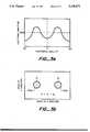
- the scattering half angle ( ⁇ s )means the square root of A/ ⁇ :
- Ain units of (degree) 2 ) is the area enclosed by the 50% contour(s), such area A corresponding to the area(s) within which the scattering is greater than 50% of the maximum.
- FIG. 4ashows the scattering diagram for a symmetric, unimodal, scattering situation.
- the 50% contourdefines an approximately circular area A, as shown in FIG. 4b.
- the scatteringis bimodal and/or asymmetric, as shown in FIG. 5a, then there are multiple areas A 1 and A 2 defined by the 50% contours, as shown in FIG. 5b, and A is their sum.
- the scattering centersshould be not so scattering such that they prevent incident light from reaching the reflector (in the instance of a reflective display) or prevent light from the light source from reaching the viewer (in the instance of a transmissive display).
- the scattering centersshould permit at least 10%, preferably at least 30% of the light impinging on them to be transmitted.
- the scattering by the scattering centers of this inventionprovide for a more pleasing display. If the degree of scattering is too low, i.e., as in prior art displays having a highly specular reflector and no scattering centers as taught in this invention, then the mirror-like reflections are not sufficiently suppressed. This effect is to some extent dependent on the size of the display. A small display, for example about 4 inches diagonal, can tolerate a lower degree of scattering than a larger display, for example about 14 inches diagonal, because the amount of structure seen in the reflector is likely to be much less.
- the brightnessis improved over a wider range of viewing angles than with a specular mirror which is only bright when the eye sees the images of the light sources in the room. Glare from the light sources is reduced, making display appearance (contrast, brightness, etc.) less dependent on the exact viewing angles and placement of the light sources in the room.
- thisdoes not mean that the higher the degree of scattering, the better the viewability of the display--rather, the degree of scattering should be within the ranges taught herein. If the degree of scattering is too high, then high angle scattered light is trapped in the display, to be absorbed by any pleochroic dye present, and the optical gain is too low for most viewing purposes.
- Silicone oil(5.50 g, refractive index 1.380 at 25° C., Petrarch Systems, Inc., Brystol, Pa.) was emulsified in 12.25 g of a solution of polyvinyl alcohol (Airvol 205, Airproducts and Chemicals, Inc., King of Prussia, Pa.) in 1:1 ethanol:water solvent to give an emulsion having a number average droplet size of 0.97 ⁇ m. Then 10.40 g water was added.
- polyvinyl alcoholAirvol 205, Airproducts and Chemicals, Inc., King of Prussia, Pa.
- This emulsion(1 part by weight) was blended with a previously prepared emulsion (6 parts by weight, volume average droplet size about 3 ⁇ m) of encapsulated nematic liquid crystal material, comprising 60% by weight water, 20% by weight Airvol 205, and 20% by weight positive dielectric nematic liquid crystal (ZLI 3401, Merck GmbH, Darmstatdt, Germany) containing 4% by weight pleochroic dye (S344, a black dichroic dye mixture from Mitsui Toatsu Dyes Ltd., Japan).
- a previously prepared emulsion(6 parts by weight, volume average droplet size about 3 ⁇ m) of encapsulated nematic liquid crystal material, comprising 60% by weight water, 20% by weight Airvol 205, and 20% by weight positive dielectric nematic liquid crystal (ZLI 3401, Merck GmbH, Darmstatdt, Germany) containing 4% by weight pleochroic dye (S344, a black dichroic dye mixture from Mitsui Toatsu Dyes Ltd.
- This blend of emulsionswas coated onto aluminum coated polyester film to give a dry film of thickness about 18 ⁇ m.
- An indium tin oxide (ITO) polyester filmwas laminated under pressure on top of the film to give a reflective liquid crystal cell. This cell initially appeared dark, but with the application of 40 volts the cell lightened up to reveal a scattering mirror-like surface with a scattering half-angle of 3.5 degrees.
- ITOindium tin oxide
- a mixture of 0.1 g hollow glass balls (Eccospheres MC-37, Emerson & Cuming, Canton, Mass.) and 3 g encapsulated liquid crystal emulsionwas hand stirred and then vortexed prior to coating.
- the glass ballshad been previously sieved through a 500 mesh screen to eliminate larger, less desirable particle sizes.
- the liquid crystalswere a nematic liquid crystal with positive dielectric anisotropy (ZLI 3401) containing 4% by weight of a pleochroic dye (S344).
- the liquid crystal emulsionhad a volume average droplet size of about 2.5 ⁇ m of encapsulated liquid crystals in a 1:2 weight ratio with 10% aqueous poly(vinyl alcohol) (Airvol 205) solution.
- the mixturewas coated onto aluminized Mylar poly(ethylene terephthalate) to give a dry film of about 20 ⁇ m thick.
- An indium tin oxide (ITO) coated polyester filmwas then laminated on top, with the ITO facing the film, under pressure to give a reflective liquid crystal display cell.
- the cellinitially appeared dark, but with the application of a voltage, the cell lightened to reveal a scattering surface.
- the brightnesswas not as high as in the cell of Example 1, possibly due to the wide range of particle sizes incorporated into the emulsion and/or the very low refractive index of air in the hollow spheres.
Landscapes
- Physics & Mathematics (AREA)
- Nonlinear Science (AREA)
- Chemical & Material Sciences (AREA)
- General Physics & Mathematics (AREA)
- Optics & Photonics (AREA)
- Dispersion Chemistry (AREA)
- Mathematical Physics (AREA)
- Crystallography & Structural Chemistry (AREA)
- Liquid Crystal (AREA)
- Electrochromic Elements, Electrophoresis, Or Variable Reflection Or Absorption Elements (AREA)
Abstract
Description
θ.sub.s =(A/π).sup.1/2
Claims (15)
Priority Applications (8)
| Application Number | Priority Date | Filing Date | Title |
|---|---|---|---|
| US07/653,563US5138472A (en) | 1991-02-11 | 1991-02-11 | Display having light scattering centers |
| CA002100336ACA2100336C (en) | 1991-02-11 | 1992-01-21 | Display having light scattering centers |
| DE69219321TDE69219321T2 (en) | 1991-02-11 | 1992-01-21 | DISPLAY DEVICE WITH LIGHT DISTRIBUTION CENTERS |
| PCT/US1992/000507WO1992014182A1 (en) | 1991-02-11 | 1992-01-21 | Display having light scattering centers |
| AT92906366TATE152252T1 (en) | 1991-02-11 | 1992-01-21 | DISPLAY DEVICE WITH LIGHT DIFFUSE CENTERS |
| JP04505691AJP3127303B2 (en) | 1991-02-11 | 1992-01-21 | Display device having light scattering nuclei |
| EP92906366AEP0571509B1 (en) | 1991-02-11 | 1992-01-21 | Display having light scattering centers |
| KR1019930702394AKR930703622A (en) | 1991-02-11 | 1993-08-11 | Display with light scattering center |
Applications Claiming Priority (1)
| Application Number | Priority Date | Filing Date | Title |
|---|---|---|---|
| US07/653,563US5138472A (en) | 1991-02-11 | 1991-02-11 | Display having light scattering centers |
Publications (1)
| Publication Number | Publication Date |
|---|---|
| US5138472Atrue US5138472A (en) | 1992-08-11 |
Family
ID=24621391
Family Applications (1)
| Application Number | Title | Priority Date | Filing Date |
|---|---|---|---|
| US07/653,563Expired - LifetimeUS5138472A (en) | 1991-02-11 | 1991-02-11 | Display having light scattering centers |
Country Status (8)
| Country | Link |
|---|---|
| US (1) | US5138472A (en) |
| EP (1) | EP0571509B1 (en) |
| JP (1) | JP3127303B2 (en) |
| KR (1) | KR930703622A (en) |
| AT (1) | ATE152252T1 (en) |
| CA (1) | CA2100336C (en) |
| DE (1) | DE69219321T2 (en) |
| WO (1) | WO1992014182A1 (en) |
Cited By (68)
| Publication number | Priority date | Publication date | Assignee | Title |
|---|---|---|---|---|
| US5202063A (en)* | 1991-02-11 | 1993-04-13 | Raychem Corporation | Method for making encapsulated liquid crystal material |
| US5216530A (en)* | 1985-06-03 | 1993-06-01 | Taliq Corporation | Encapsulated liquid crystal having a smectic phase |
| US5233445A (en)* | 1991-12-12 | 1993-08-03 | Raychem Corporation | Active matrix liquid crystal display with average dielectric constant greater than 6 and less than 1.8 meq/g cyano groups |
| WO1993023496A1 (en)* | 1992-05-18 | 1993-11-25 | Kent State University | Liquid crystalline light modulating device & material |
| US5307187A (en)* | 1991-06-28 | 1994-04-26 | Kabushiki Kaisha Toshiba | Liquid crystal element with higher resistivity in the encapsulation medium than in the liquid crystal |
| US5335101A (en)* | 1993-05-06 | 1994-08-02 | Raychem Corporation | Method of making liquid crystal material including polymerizing dispersion of prepolymer and liquid crystal which is immiscible in the prepolymer |
| US5499121A (en)* | 1993-03-18 | 1996-03-12 | Boit Inc. | Color variance polymer matrix display having two scattering states or N.sub.<or> both NE and NO |
| US5654784A (en)* | 1992-10-24 | 1997-08-05 | Sony Corporation | Liquid crystal devices comprising a multitude of domains having different threshold voltages for switching liquid crystals |
| US5668614A (en)* | 1995-05-01 | 1997-09-16 | Kent State University | Pixelized liquid crystal display materials including chiral material adopted to change its chirality upon photo-irradiation |
| US5691795A (en)* | 1991-05-02 | 1997-11-25 | Kent State University | Polymer stabilized liquid crystalline light modulating device and material |
| US5695682A (en)* | 1991-05-02 | 1997-12-09 | Kent State University | Liquid crystalline light modulating device and material |
| US5729320A (en)* | 1990-10-12 | 1998-03-17 | Rudolf Eidenschink | Liquid crystalline medium including closely packed particles and method for generating images using same |
| US5812230A (en)* | 1995-12-27 | 1998-09-22 | Sharp Kabushiki Kaisha | Liquid crystal display and manufacturing method thereof with isotropic microstructural elements between smectic layers |
| US5831698A (en)* | 1996-08-20 | 1998-11-03 | International Business Machines Corporation | Electrically variable diffuser |
| US5847798A (en)* | 1991-05-02 | 1998-12-08 | Kent State University | Polymer stabilized black-white cholesteric reflective display |
| US5872607A (en)* | 1994-12-27 | 1999-02-16 | Seiko Epson Corporation | Liquid crystal display device and method for producing such |
| US5905552A (en)* | 1992-11-09 | 1999-05-18 | Casio Computer Co., Ltd. | Polymer dispersed liquid crystal display device |
| US6067185A (en)* | 1997-08-28 | 2000-05-23 | E Ink Corporation | Process for creating an encapsulated electrophoretic display |
| US6120839A (en) | 1995-07-20 | 2000-09-19 | E Ink Corporation | Electro-osmotic displays and materials for making the same |
| US6249271B1 (en) | 1995-07-20 | 2001-06-19 | E Ink Corporation | Retroreflective electrophoretic displays and materials for making the same |
| US6262833B1 (en) | 1998-10-07 | 2001-07-17 | E Ink Corporation | Capsules for electrophoretic displays and methods for making the same |
| US6262706B1 (en) | 1995-07-20 | 2001-07-17 | E Ink Corporation | Retroreflective electrophoretic displays and materials for making the same |
| US6300932B1 (en) | 1997-08-28 | 2001-10-09 | E Ink Corporation | Electrophoretic displays with luminescent particles and materials for making the same |
| US6377387B1 (en) | 1999-04-06 | 2002-04-23 | E Ink Corporation | Methods for producing droplets for use in capsule-based electrophoretic displays |
| US6376828B1 (en) | 1998-10-07 | 2002-04-23 | E Ink Corporation | Illumination system for nonemissive electronic displays |
| US6445489B1 (en) | 1998-03-18 | 2002-09-03 | E Ink Corporation | Electrophoretic displays and systems for addressing such displays |
| US20020154382A1 (en)* | 2001-04-19 | 2002-10-24 | Morrison Ian D. | Electrochromic-nanoparticle displays |
| US6473072B1 (en) | 1998-05-12 | 2002-10-29 | E Ink Corporation | Microencapsulated electrophoretic electrostatically-addressed media for drawing device applications |
| US6498114B1 (en) | 1999-04-09 | 2002-12-24 | E Ink Corporation | Method for forming a patterned semiconductor film |
| US6515649B1 (en)* | 1995-07-20 | 2003-02-04 | E Ink Corporation | Suspended particle displays and materials for making the same |
| US6518949B2 (en) | 1998-04-10 | 2003-02-11 | E Ink Corporation | Electronic displays using organic-based field effect transistors |
| US20030053008A1 (en)* | 2001-09-19 | 2003-03-20 | Shoji Nakano | Reflection sheet and backlight unit using the same |
| US20030214695A1 (en)* | 2002-03-18 | 2003-11-20 | E Ink Corporation | Electro-optic displays, and methods for driving same |
| WO2002084695A3 (en)* | 2001-04-17 | 2003-11-27 | Koninkl Philips Electronics Nv | Liquid crystal shutter laminated on display panel of display device |
| USD485294S1 (en) | 1998-07-22 | 2004-01-13 | E Ink Corporation | Electrode structure for an electronic display |
| US6693620B1 (en) | 1999-05-03 | 2004-02-17 | E Ink Corporation | Threshold addressing of electrophoretic displays |
| US6704133B2 (en) | 1998-03-18 | 2004-03-09 | E-Ink Corporation | Electro-optic display overlays and systems for addressing such displays |
| US20040052079A1 (en)* | 2001-05-08 | 2004-03-18 | Shoji Nakano | Reflection sheet and backlight unit using the same |
| US6727881B1 (en) | 1995-07-20 | 2004-04-27 | E Ink Corporation | Encapsulated electrophoretic displays and methods and materials for making the same |
| US6750843B2 (en)* | 2000-09-05 | 2004-06-15 | Fuji Xerox Co., Ltd. | Display device |
| US6839158B2 (en) | 1997-08-28 | 2005-01-04 | E Ink Corporation | Encapsulated electrophoretic displays having a monolayer of capsules and materials and methods for making the same |
| US6842657B1 (en) | 1999-04-09 | 2005-01-11 | E Ink Corporation | Reactive formation of dielectric layers and protection of organic layers in organic semiconductor device fabrication |
| US20050036090A1 (en)* | 2002-02-12 | 2005-02-17 | Seiko Epson Corporation | Method for manufacturing electrooptical device and apparatus for manufacturing the same, electrooptical device and electronic appliances |
| US6864875B2 (en) | 1998-04-10 | 2005-03-08 | E Ink Corporation | Full color reflective display with multichromatic sub-pixels |
| US6865010B2 (en) | 2001-12-13 | 2005-03-08 | E Ink Corporation | Electrophoretic electronic displays with low-index films |
| US7002728B2 (en) | 1997-08-28 | 2006-02-21 | E Ink Corporation | Electrophoretic particles, and processes for the production thereof |
| US20060087865A1 (en)* | 2004-10-26 | 2006-04-27 | Ju-Hwa Ha | Light modulating plate, backlight assembly having the same and display device having the same |
| US7038655B2 (en) | 1999-05-03 | 2006-05-02 | E Ink Corporation | Electrophoretic ink composed of particles with field dependent mobilities |
| US7071913B2 (en) | 1995-07-20 | 2006-07-04 | E Ink Corporation | Retroreflective electrophoretic displays and materials for making the same |
| US7109968B2 (en) | 1995-07-20 | 2006-09-19 | E Ink Corporation | Non-spherical cavity electrophoretic displays and methods and materials for making the same |
| US7167155B1 (en)* | 1995-07-20 | 2007-01-23 | E Ink Corporation | Color electrophoretic displays |
| US7230750B2 (en) | 2001-05-15 | 2007-06-12 | E Ink Corporation | Electrophoretic media and processes for the production thereof |
| US20070146887A1 (en)* | 2003-12-26 | 2007-06-28 | Fuji Photo Film Co., Ltd. | Antireflection film, polarizing plate, method for producing them, liquid cryatal display element, liquid crystal display device, and image display device |
| US7242513B2 (en) | 1997-08-28 | 2007-07-10 | E Ink Corporation | Encapsulated electrophoretic displays having a monolayer of capsules and materials and methods for making the same |
| US7247379B2 (en) | 1997-08-28 | 2007-07-24 | E Ink Corporation | Electrophoretic particles, and processes for the production thereof |
| US7256766B2 (en)* | 1998-08-27 | 2007-08-14 | E Ink Corporation | Electrophoretic display comprising optical biasing element |
| US7312916B2 (en) | 2002-08-07 | 2007-12-25 | E Ink Corporation | Electrophoretic media containing specularly reflective particles |
| US7327511B2 (en) | 2004-03-23 | 2008-02-05 | E Ink Corporation | Light modulators |
| US7411719B2 (en) | 1995-07-20 | 2008-08-12 | E Ink Corporation | Electrophoretic medium and process for the production thereof |
| US7492497B2 (en) | 2006-08-02 | 2009-02-17 | E Ink Corporation | Multi-layer light modulator |
| US20090168183A1 (en)* | 2007-12-31 | 2009-07-02 | Seung-Mo Kim | Optical member and display having the same |
| US7667684B2 (en) | 1998-07-08 | 2010-02-23 | E Ink Corporation | Methods for achieving improved color in microencapsulated electrophoretic devices |
| WO2011075134A1 (en)* | 2009-12-18 | 2011-06-23 | Hewlett-Packard Development Company, L.P. | Reflective display |
| US7999787B2 (en) | 1995-07-20 | 2011-08-16 | E Ink Corporation | Methods for driving electrophoretic displays using dielectrophoretic forces |
| US8115729B2 (en) | 1999-05-03 | 2012-02-14 | E Ink Corporation | Electrophoretic display element with filler particles |
| US9005494B2 (en) | 2004-01-20 | 2015-04-14 | E Ink Corporation | Preparation of capsules |
| US10331005B2 (en) | 2002-10-16 | 2019-06-25 | E Ink Corporation | Electrophoretic displays |
| US11250794B2 (en) | 2004-07-27 | 2022-02-15 | E Ink Corporation | Methods for driving electrophoretic displays using dielectrophoretic forces |
Families Citing this family (4)
| Publication number | Priority date | Publication date | Assignee | Title |
|---|---|---|---|---|
| US5629783A (en)* | 1993-10-05 | 1997-05-13 | Casio Computer Co., Ltd. | Active matrix polymer dispersed liquid crystal display device with flourescent film |
| JP3068400B2 (en)* | 1994-03-17 | 2000-07-24 | シャープ株式会社 | Manufacturing method of liquid crystal display device |
| JP2998075B2 (en)* | 1996-06-20 | 2000-01-11 | セイコーインスツルメンツ株式会社 | Reflective liquid crystal display |
| CN109827096A (en)* | 2019-01-23 | 2019-05-31 | 厦门大学 | A laser lighting assembly using hollow alumina microspheres and its manufacturing method |
Citations (16)
| Publication number | Priority date | Publication date | Assignee | Title |
|---|---|---|---|---|
| US3905682A (en)* | 1974-06-14 | 1975-09-16 | Rca Corp | Liquid crystal devices of improved contrast |
| US3984176A (en)* | 1974-01-31 | 1976-10-05 | Kabushiki Kaisha Daini Seikosha | Reflective plates for a liquid crystal display device |
| JPS535996A (en)* | 1976-07-06 | 1978-01-19 | Seiko Epson Corp | Reflecting plate for liquid crystal display device |
| US4435047A (en)* | 1981-09-16 | 1984-03-06 | Manchester R & D Partnership | Encapsulated liquid crystal and method |
| US4591233A (en)* | 1983-03-21 | 1986-05-27 | Manchester R & D Partnership | Enhanced scattering in voltage sensitive encapsulated liquid crystal with spaced apart absorber |
| US4606611A (en)* | 1981-09-16 | 1986-08-19 | Manchester R & D Partnership | Enhanced scattering in voltage sensitive encapsulated liquid crystal |
| US4648691A (en)* | 1979-12-27 | 1987-03-10 | Seiko Epson Kabushiki Kaisha | Liquid crystal display device having diffusely reflective picture electrode and pleochroic dye |
| US4671618A (en)* | 1986-05-22 | 1987-06-09 | Wu Bao Gang | Liquid crystalline-plastic material having submillisecond switch times and extended memory |
| US4673255A (en)* | 1986-05-22 | 1987-06-16 | John West | Method of controlling microdroplet growth in polymeric dispersed liquid crystal |
| US4685771A (en)* | 1985-09-17 | 1987-08-11 | West John L | Liquid crystal display material comprising a liquid crystal dispersion in a thermoplastic resin |
| US4688900A (en)* | 1984-03-19 | 1987-08-25 | Kent State University | Light modulating material comprising a liquid crystal dispersion in a plastic matrix |
| US4707080A (en)* | 1981-09-16 | 1987-11-17 | Manchester R & D Partnership | Encapsulated liquid crystal material, apparatus and method |
| US4832458A (en)* | 1984-08-28 | 1989-05-23 | Talig Corporation | Display for contrast enhancement |
| EP0326248A2 (en)* | 1988-01-25 | 1989-08-02 | Raychem Corporation | Visual display |
| WO1990003593A1 (en)* | 1988-09-28 | 1990-04-05 | Taliq Corporation | Enhanced backscattering and light transmission in a guest host display |
| US5088807A (en)* | 1988-05-23 | 1992-02-18 | Imperial Chemical Industries Plc | Liquid crystal devices |
Family Cites Families (1)
| Publication number | Priority date | Publication date | Assignee | Title |
|---|---|---|---|---|
| JPS535996B2 (en)* | 1974-03-11 | 1978-03-03 |
- 1991
- 1991-02-11USUS07/653,563patent/US5138472A/ennot_activeExpired - Lifetime
- 1992
- 1992-01-21WOPCT/US1992/000507patent/WO1992014182A1/enactiveIP Right Grant
- 1992-01-21JPJP04505691Apatent/JP3127303B2/ennot_activeExpired - Lifetime
- 1992-01-21CACA002100336Apatent/CA2100336C/ennot_activeExpired - Lifetime
- 1992-01-21EPEP92906366Apatent/EP0571509B1/ennot_activeExpired - Lifetime
- 1992-01-21ATAT92906366Tpatent/ATE152252T1/ennot_activeIP Right Cessation
- 1992-01-21DEDE69219321Tpatent/DE69219321T2/ennot_activeExpired - Lifetime
- 1993
- 1993-08-11KRKR1019930702394Apatent/KR930703622A/ennot_activeCeased
Patent Citations (17)
| Publication number | Priority date | Publication date | Assignee | Title |
|---|---|---|---|---|
| US3984176A (en)* | 1974-01-31 | 1976-10-05 | Kabushiki Kaisha Daini Seikosha | Reflective plates for a liquid crystal display device |
| US3905682A (en)* | 1974-06-14 | 1975-09-16 | Rca Corp | Liquid crystal devices of improved contrast |
| JPS535996A (en)* | 1976-07-06 | 1978-01-19 | Seiko Epson Corp | Reflecting plate for liquid crystal display device |
| US4648691A (en)* | 1979-12-27 | 1987-03-10 | Seiko Epson Kabushiki Kaisha | Liquid crystal display device having diffusely reflective picture electrode and pleochroic dye |
| US4707080A (en)* | 1981-09-16 | 1987-11-17 | Manchester R & D Partnership | Encapsulated liquid crystal material, apparatus and method |
| US4435047A (en)* | 1981-09-16 | 1984-03-06 | Manchester R & D Partnership | Encapsulated liquid crystal and method |
| US4606611A (en)* | 1981-09-16 | 1986-08-19 | Manchester R & D Partnership | Enhanced scattering in voltage sensitive encapsulated liquid crystal |
| US4616903A (en)* | 1981-09-16 | 1986-10-14 | Manchester R & D Partnership | Encapsulated liquid crystal and method |
| US4591233A (en)* | 1983-03-21 | 1986-05-27 | Manchester R & D Partnership | Enhanced scattering in voltage sensitive encapsulated liquid crystal with spaced apart absorber |
| US4688900A (en)* | 1984-03-19 | 1987-08-25 | Kent State University | Light modulating material comprising a liquid crystal dispersion in a plastic matrix |
| US4832458A (en)* | 1984-08-28 | 1989-05-23 | Talig Corporation | Display for contrast enhancement |
| US4685771A (en)* | 1985-09-17 | 1987-08-11 | West John L | Liquid crystal display material comprising a liquid crystal dispersion in a thermoplastic resin |
| US4673255A (en)* | 1986-05-22 | 1987-06-16 | John West | Method of controlling microdroplet growth in polymeric dispersed liquid crystal |
| US4671618A (en)* | 1986-05-22 | 1987-06-09 | Wu Bao Gang | Liquid crystalline-plastic material having submillisecond switch times and extended memory |
| EP0326248A2 (en)* | 1988-01-25 | 1989-08-02 | Raychem Corporation | Visual display |
| US5088807A (en)* | 1988-05-23 | 1992-02-18 | Imperial Chemical Industries Plc | Liquid crystal devices |
| WO1990003593A1 (en)* | 1988-09-28 | 1990-04-05 | Taliq Corporation | Enhanced backscattering and light transmission in a guest host display |
Non-Patent Citations (6)
| Title |
|---|
| Haas, "Scattering Electro-Optic Cells," Xerox Disclosure Journal, vol. 3, No. 5, Sep./Oct. 1978, pp. 333-334. |
| Haas, Scattering Electro Optic Cells, Xerox Disclosure Journal, vol. 3, No. 5, Sep./Oct. 1978, pp. 333 334.* |
| J. Applied Phys. 62(9); Angular discrimination of light transmission through polymer dispersed liquid crystal films; Wu et al.; pp. 3925 3931 (1987).* |
| J. Applied Phys. 62(9); Angular discrimination of light transmission through polymer-dispersed liquid-crystal films; Wu et al.; pp. 3925-3931 (1987). |
| The Physics and Chemistry of Liquid Crystal Devices; IBM Research Library; pp. 190 194 (1979).* |
| The Physics and Chemistry of Liquid Crystal Devices; IBM Research Library; pp. 190-194 (1979). |
Cited By (91)
| Publication number | Priority date | Publication date | Assignee | Title |
|---|---|---|---|---|
| US5216530A (en)* | 1985-06-03 | 1993-06-01 | Taliq Corporation | Encapsulated liquid crystal having a smectic phase |
| US5729320A (en)* | 1990-10-12 | 1998-03-17 | Rudolf Eidenschink | Liquid crystalline medium including closely packed particles and method for generating images using same |
| US5202063A (en)* | 1991-02-11 | 1993-04-13 | Raychem Corporation | Method for making encapsulated liquid crystal material |
| US5691795A (en)* | 1991-05-02 | 1997-11-25 | Kent State University | Polymer stabilized liquid crystalline light modulating device and material |
| US5847798A (en)* | 1991-05-02 | 1998-12-08 | Kent State University | Polymer stabilized black-white cholesteric reflective display |
| US5695682A (en)* | 1991-05-02 | 1997-12-09 | Kent State University | Liquid crystalline light modulating device and material |
| US5437811A (en)* | 1991-05-02 | 1995-08-01 | Kent State University | Liquid crystalline light modulating device and material |
| US5307187A (en)* | 1991-06-28 | 1994-04-26 | Kabushiki Kaisha Toshiba | Liquid crystal element with higher resistivity in the encapsulation medium than in the liquid crystal |
| US5233445A (en)* | 1991-12-12 | 1993-08-03 | Raychem Corporation | Active matrix liquid crystal display with average dielectric constant greater than 6 and less than 1.8 meq/g cyano groups |
| WO1993023496A1 (en)* | 1992-05-18 | 1993-11-25 | Kent State University | Liquid crystalline light modulating device & material |
| US5654784A (en)* | 1992-10-24 | 1997-08-05 | Sony Corporation | Liquid crystal devices comprising a multitude of domains having different threshold voltages for switching liquid crystals |
| US6040884A (en)* | 1992-10-24 | 2000-03-21 | Sony Corporation | Liquid crystal devices comprising a multitude of domains having different threshold voltages for switching liquid crystals |
| US5905552A (en)* | 1992-11-09 | 1999-05-18 | Casio Computer Co., Ltd. | Polymer dispersed liquid crystal display device |
| US5499121A (en)* | 1993-03-18 | 1996-03-12 | Boit Inc. | Color variance polymer matrix display having two scattering states or N.sub.<or> both NE and NO |
| US5335101A (en)* | 1993-05-06 | 1994-08-02 | Raychem Corporation | Method of making liquid crystal material including polymerizing dispersion of prepolymer and liquid crystal which is immiscible in the prepolymer |
| US5872607A (en)* | 1994-12-27 | 1999-02-16 | Seiko Epson Corporation | Liquid crystal display device and method for producing such |
| US5668614A (en)* | 1995-05-01 | 1997-09-16 | Kent State University | Pixelized liquid crystal display materials including chiral material adopted to change its chirality upon photo-irradiation |
| US8593718B2 (en) | 1995-07-20 | 2013-11-26 | E Ink Corporation | Electro-osmotic displays and materials for making the same |
| US6727881B1 (en) | 1995-07-20 | 2004-04-27 | E Ink Corporation | Encapsulated electrophoretic displays and methods and materials for making the same |
| US7071913B2 (en) | 1995-07-20 | 2006-07-04 | E Ink Corporation | Retroreflective electrophoretic displays and materials for making the same |
| US6120839A (en) | 1995-07-20 | 2000-09-19 | E Ink Corporation | Electro-osmotic displays and materials for making the same |
| US6249271B1 (en) | 1995-07-20 | 2001-06-19 | E Ink Corporation | Retroreflective electrophoretic displays and materials for making the same |
| US6515649B1 (en)* | 1995-07-20 | 2003-02-04 | E Ink Corporation | Suspended particle displays and materials for making the same |
| US6262706B1 (en) | 1995-07-20 | 2001-07-17 | E Ink Corporation | Retroreflective electrophoretic displays and materials for making the same |
| US7391555B2 (en) | 1995-07-20 | 2008-06-24 | E Ink Corporation | Non-spherical cavity electrophoretic displays and materials for making the same |
| US7411719B2 (en) | 1995-07-20 | 2008-08-12 | E Ink Corporation | Electrophoretic medium and process for the production thereof |
| US7999787B2 (en) | 1995-07-20 | 2011-08-16 | E Ink Corporation | Methods for driving electrophoretic displays using dielectrophoretic forces |
| US7109968B2 (en) | 1995-07-20 | 2006-09-19 | E Ink Corporation | Non-spherical cavity electrophoretic displays and methods and materials for making the same |
| US7167155B1 (en)* | 1995-07-20 | 2007-01-23 | E Ink Corporation | Color electrophoretic displays |
| US7848007B2 (en) | 1995-07-20 | 2010-12-07 | E Ink Corporation | Electrophoretic medium and process for the production thereof |
| US7746544B2 (en) | 1995-07-20 | 2010-06-29 | E Ink Corporation | Electro-osmotic displays and materials for making the same |
| US5812230A (en)* | 1995-12-27 | 1998-09-22 | Sharp Kabushiki Kaisha | Liquid crystal display and manufacturing method thereof with isotropic microstructural elements between smectic layers |
| US5831698A (en)* | 1996-08-20 | 1998-11-03 | International Business Machines Corporation | Electrically variable diffuser |
| US6300932B1 (en) | 1997-08-28 | 2001-10-09 | E Ink Corporation | Electrophoretic displays with luminescent particles and materials for making the same |
| US7002728B2 (en) | 1997-08-28 | 2006-02-21 | E Ink Corporation | Electrophoretic particles, and processes for the production thereof |
| US7247379B2 (en) | 1997-08-28 | 2007-07-24 | E Ink Corporation | Electrophoretic particles, and processes for the production thereof |
| US7242513B2 (en) | 1997-08-28 | 2007-07-10 | E Ink Corporation | Encapsulated electrophoretic displays having a monolayer of capsules and materials and methods for making the same |
| US6392785B1 (en) | 1997-08-28 | 2002-05-21 | E Ink Corporation | Non-spherical cavity electrophoretic displays and materials for making the same |
| US6839158B2 (en) | 1997-08-28 | 2005-01-04 | E Ink Corporation | Encapsulated electrophoretic displays having a monolayer of capsules and materials and methods for making the same |
| US6067185A (en)* | 1997-08-28 | 2000-05-23 | E Ink Corporation | Process for creating an encapsulated electrophoretic display |
| US6445489B1 (en) | 1998-03-18 | 2002-09-03 | E Ink Corporation | Electrophoretic displays and systems for addressing such displays |
| US6704133B2 (en) | 1998-03-18 | 2004-03-09 | E-Ink Corporation | Electro-optic display overlays and systems for addressing such displays |
| US8466852B2 (en) | 1998-04-10 | 2013-06-18 | E Ink Corporation | Full color reflective display with multichromatic sub-pixels |
| US7075502B1 (en) | 1998-04-10 | 2006-07-11 | E Ink Corporation | Full color reflective display with multichromatic sub-pixels |
| US6518949B2 (en) | 1998-04-10 | 2003-02-11 | E Ink Corporation | Electronic displays using organic-based field effect transistors |
| US6864875B2 (en) | 1998-04-10 | 2005-03-08 | E Ink Corporation | Full color reflective display with multichromatic sub-pixels |
| US6738050B2 (en) | 1998-05-12 | 2004-05-18 | E Ink Corporation | Microencapsulated electrophoretic electrostatically addressed media for drawing device applications |
| US6473072B1 (en) | 1998-05-12 | 2002-10-29 | E Ink Corporation | Microencapsulated electrophoretic electrostatically-addressed media for drawing device applications |
| US9293511B2 (en) | 1998-07-08 | 2016-03-22 | E Ink Corporation | Methods for achieving improved color in microencapsulated electrophoretic devices |
| US7667684B2 (en) | 1998-07-08 | 2010-02-23 | E Ink Corporation | Methods for achieving improved color in microencapsulated electrophoretic devices |
| USD485294S1 (en) | 1998-07-22 | 2004-01-13 | E Ink Corporation | Electrode structure for an electronic display |
| US7256766B2 (en)* | 1998-08-27 | 2007-08-14 | E Ink Corporation | Electrophoretic display comprising optical biasing element |
| US6376828B1 (en) | 1998-10-07 | 2002-04-23 | E Ink Corporation | Illumination system for nonemissive electronic displays |
| US6262833B1 (en) | 1998-10-07 | 2001-07-17 | E Ink Corporation | Capsules for electrophoretic displays and methods for making the same |
| US6377387B1 (en) | 1999-04-06 | 2002-04-23 | E Ink Corporation | Methods for producing droplets for use in capsule-based electrophoretic displays |
| US6842657B1 (en) | 1999-04-09 | 2005-01-11 | E Ink Corporation | Reactive formation of dielectric layers and protection of organic layers in organic semiconductor device fabrication |
| US6498114B1 (en) | 1999-04-09 | 2002-12-24 | E Ink Corporation | Method for forming a patterned semiconductor film |
| US8115729B2 (en) | 1999-05-03 | 2012-02-14 | E Ink Corporation | Electrophoretic display element with filler particles |
| US7038655B2 (en) | 1999-05-03 | 2006-05-02 | E Ink Corporation | Electrophoretic ink composed of particles with field dependent mobilities |
| US6693620B1 (en) | 1999-05-03 | 2004-02-17 | E Ink Corporation | Threshold addressing of electrophoretic displays |
| US6750843B2 (en)* | 2000-09-05 | 2004-06-15 | Fuji Xerox Co., Ltd. | Display device |
| WO2002084695A3 (en)* | 2001-04-17 | 2003-11-27 | Koninkl Philips Electronics Nv | Liquid crystal shutter laminated on display panel of display device |
| US20020154382A1 (en)* | 2001-04-19 | 2002-10-24 | Morrison Ian D. | Electrochromic-nanoparticle displays |
| US20030189749A1 (en)* | 2001-04-19 | 2003-10-09 | E Ink Corporation | Electrochromic-nanoparticle displays |
| US7180649B2 (en) | 2001-04-19 | 2007-02-20 | E Ink Corporation | Electrochromic-nanoparticle displays |
| US6943855B2 (en)* | 2001-05-08 | 2005-09-13 | Keiwa Inc. | Reflection sheet and backlight unit using the same |
| US20040052079A1 (en)* | 2001-05-08 | 2004-03-18 | Shoji Nakano | Reflection sheet and backlight unit using the same |
| US7375875B2 (en) | 2001-05-15 | 2008-05-20 | E Ink Corporation | Electrophoretic media and processes for the production thereof |
| US7230750B2 (en) | 2001-05-15 | 2007-06-12 | E Ink Corporation | Electrophoretic media and processes for the production thereof |
| US7532388B2 (en) | 2001-05-15 | 2009-05-12 | E Ink Corporation | Electrophoretic media and processes for the production thereof |
| US6906761B2 (en) | 2001-09-19 | 2005-06-14 | Keiwa Inc. | Reflection sheet and backlight unit using the same |
| US20030053008A1 (en)* | 2001-09-19 | 2003-03-20 | Shoji Nakano | Reflection sheet and backlight unit using the same |
| US6865010B2 (en) | 2001-12-13 | 2005-03-08 | E Ink Corporation | Electrophoretic electronic displays with low-index films |
| US20050036090A1 (en)* | 2002-02-12 | 2005-02-17 | Seiko Epson Corporation | Method for manufacturing electrooptical device and apparatus for manufacturing the same, electrooptical device and electronic appliances |
| US7317281B2 (en)* | 2002-02-12 | 2008-01-08 | Seiko Epson Corporation | Method for manufacturing electrooptical device and apparatus for manufacturing the same, electrooptical device and electronic appliances |
| US20030214695A1 (en)* | 2002-03-18 | 2003-11-20 | E Ink Corporation | Electro-optic displays, and methods for driving same |
| US20050152018A1 (en)* | 2002-03-18 | 2005-07-14 | E Ink Corporation | Electro-optic displays, and methods for driving same |
| US6950220B2 (en) | 2002-03-18 | 2005-09-27 | E Ink Corporation | Electro-optic displays, and methods for driving same |
| US7787169B2 (en) | 2002-03-18 | 2010-08-31 | E Ink Corporation | Electro-optic displays, and methods for driving same |
| US7312916B2 (en) | 2002-08-07 | 2007-12-25 | E Ink Corporation | Electrophoretic media containing specularly reflective particles |
| US10331005B2 (en) | 2002-10-16 | 2019-06-25 | E Ink Corporation | Electrophoretic displays |
| US20070146887A1 (en)* | 2003-12-26 | 2007-06-28 | Fuji Photo Film Co., Ltd. | Antireflection film, polarizing plate, method for producing them, liquid cryatal display element, liquid crystal display device, and image display device |
| US8039065B2 (en)* | 2003-12-26 | 2011-10-18 | Fujifilm Corporation | Antireflection film, polarizing plate, method for producing them, liquid crystal display element, liquid crystal display device, and image display device |
| US9005494B2 (en) | 2004-01-20 | 2015-04-14 | E Ink Corporation | Preparation of capsules |
| US7327511B2 (en) | 2004-03-23 | 2008-02-05 | E Ink Corporation | Light modulators |
| US11250794B2 (en) | 2004-07-27 | 2022-02-15 | E Ink Corporation | Methods for driving electrophoretic displays using dielectrophoretic forces |
| US7569257B2 (en)* | 2004-10-26 | 2009-08-04 | Samsung Electronics Co., Ltd. | Light modulating plate, backlight assembly having the same and display device having the same |
| US20060087865A1 (en)* | 2004-10-26 | 2006-04-27 | Ju-Hwa Ha | Light modulating plate, backlight assembly having the same and display device having the same |
| US7492497B2 (en) | 2006-08-02 | 2009-02-17 | E Ink Corporation | Multi-layer light modulator |
| US20090168183A1 (en)* | 2007-12-31 | 2009-07-02 | Seung-Mo Kim | Optical member and display having the same |
| WO2011075134A1 (en)* | 2009-12-18 | 2011-06-23 | Hewlett-Packard Development Company, L.P. | Reflective display |
Also Published As
| Publication number | Publication date |
|---|---|
| CA2100336C (en) | 2001-11-06 |
| KR930703622A (en) | 1993-11-30 |
| ATE152252T1 (en) | 1997-05-15 |
| DE69219321T2 (en) | 1997-11-20 |
| CA2100336A1 (en) | 1992-08-12 |
| WO1992014182A1 (en) | 1992-08-20 |
| JP3127303B2 (en) | 2001-01-22 |
| DE69219321D1 (en) | 1997-05-28 |
| EP0571509A4 (en) | 1994-01-05 |
| JPH06505348A (en) | 1994-06-16 |
| EP0571509A1 (en) | 1993-12-01 |
| EP0571509B1 (en) | 1997-04-23 |
Similar Documents
| Publication | Publication Date | Title |
|---|---|---|
| US5138472A (en) | Display having light scattering centers | |
| US4693560A (en) | Double layer display | |
| US4772102A (en) | Display with light traps between reflector and scattering means | |
| US4832458A (en) | Display for contrast enhancement | |
| US5285299A (en) | Encapsulated liquid crystal apparatus having low off-axis haze, operable by a sine-wave power source and including a dye | |
| US4824208A (en) | Display for contrast enhancement | |
| US4732456A (en) | Scattering display for contrast enhancement including target | |
| US4726662A (en) | Display including a prismatic lens system or a prismatic reflective system | |
| JP2857159B2 (en) | Gain reflector and liquid crystal display | |
| US5076668A (en) | Gain reflector-liquid crystal display | |
| US6067143A (en) | High contrast micro display with off-axis illumination | |
| Spruce et al. | Polymer dispersed liquid crystal (PDLC) films | |
| KR100320157B1 (en) | Chiral nematic liquid crystal composition and devices comprising the same | |
| JPH06510139A (en) | General purpose liquid crystal display device | |
| EP0571459B1 (en) | Display having light scattering electro-optical element | |
| WO1993016410A1 (en) | Front lit liquid crystal displays | |
| JP2000347223A (en) | Liquid crystal dimming body | |
| JP3758634B2 (en) | Liquid crystal display element | |
| JP3205132B2 (en) | Liquid crystal display device | |
| EP0225410A1 (en) | Display with means for contrast enhancement |
Legal Events
| Date | Code | Title | Description |
|---|---|---|---|
| AS | Assignment | Owner name:RAYCHEM CORPORATION, 300 CONSTITUTION DRIVE, MENLO Free format text:ASSIGNMENT OF ASSIGNORS INTEREST.;ASSIGNORS:JONES, PHILIP J.;TOMITA, AKIRA;WARTENBERG, MARK F.;REEL/FRAME:005613/0676 Effective date:19910211 | |
| STCF | Information on status: patent grant | Free format text:PATENTED CASE | |
| FPAY | Fee payment | Year of fee payment:4 | |
| FPAY | Fee payment | Year of fee payment:8 | |
| AS | Assignment | Owner name:TYCO INTERNATIONAL LTD., A CORPORATION OF BERMUDA, Free format text:MERGER & REORGANIZATION;ASSIGNOR:RAYCHEM CORPORATION, A CORPORATION OF DELAWARE;REEL/FRAME:011682/0001 Effective date:19990812 Owner name:AMP INCORPORATED, A CORPORATION OF PENNSYLVANIA, P Free format text:MERGER & REORGANIZATION;ASSIGNOR:RAYCHEM CORPORATION, A CORPORATION OF DELAWARE;REEL/FRAME:011682/0001 Effective date:19990812 Owner name:TYCO INTERNATIONAL (PA), INC., A CORPORATION OF NE Free format text:MERGER & REORGANIZATION;ASSIGNOR:RAYCHEM CORPORATION, A CORPORATION OF DELAWARE;REEL/FRAME:011682/0001 Effective date:19990812 | |
| AS | Assignment | Owner name:TYCO ELECTRONICS CORPORATION, A CORPORATION OF PEN Free format text:CHANGE OF NAME;ASSIGNOR:AMP INCORPORATED, A CORPORATION OF PENNSYLVANIA;REEL/FRAME:011675/0436 Effective date:19990913 | |
| FPAY | Fee payment | Year of fee payment:12 |