US5138237A - Field emission electron device employing a modulatable diamond semiconductor emitter - Google Patents
Field emission electron device employing a modulatable diamond semiconductor emitterDownload PDFInfo
- Publication number
- US5138237A US5138237AUS07/747,564US74756491AUS5138237AUS 5138237 AUS5138237 AUS 5138237AUS 74756491 AUS74756491 AUS 74756491AUS 5138237 AUS5138237 AUS 5138237A
- Authority
- US
- United States
- Prior art keywords
- layer
- electron emitter
- diamond semiconductor
- conductive
- major surface
- Prior art date
- Legal status (The legal status is an assumption and is not a legal conclusion. Google has not performed a legal analysis and makes no representation as to the accuracy of the status listed.)
- Expired - Fee Related
Links
Images


Classifications
- H—ELECTRICITY
- H01—ELECTRIC ELEMENTS
- H01J—ELECTRIC DISCHARGE TUBES OR DISCHARGE LAMPS
- H01J1/00—Details of electrodes, of magnetic control means, of screens, or of the mounting or spacing thereof, common to two or more basic types of discharge tubes or lamps
- H01J1/02—Main electrodes
- H01J1/30—Cold cathodes, e.g. field-emissive cathode
- H01J1/304—Field-emissive cathodes
- H01J1/3042—Field-emissive cathodes microengineered, e.g. Spindt-type
- H—ELECTRICITY
- H01—ELECTRIC ELEMENTS
- H01J—ELECTRIC DISCHARGE TUBES OR DISCHARGE LAMPS
- H01J3/00—Details of electron-optical or ion-optical arrangements or of ion traps common to two or more basic types of discharge tubes or lamps
- H01J3/02—Electron guns
- H01J3/021—Electron guns using a field emission, photo emission, or secondary emission electron source
- H01J3/022—Electron guns using a field emission, photo emission, or secondary emission electron source with microengineered cathode, e.g. Spindt-type
- H—ELECTRICITY
- H01—ELECTRIC ELEMENTS
- H01J—ELECTRIC DISCHARGE TUBES OR DISCHARGE LAMPS
- H01J2201/00—Electrodes common to discharge tubes
- H01J2201/30—Cold cathodes
- H01J2201/304—Field emission cathodes
- H01J2201/30446—Field emission cathodes characterised by the emitter material
- H01J2201/30453—Carbon types
- H01J2201/30457—Diamond
- H—ELECTRICITY
- H01—ELECTRIC ELEMENTS
- H01J—ELECTRIC DISCHARGE TUBES OR DISCHARGE LAMPS
- H01J2201/00—Electrodes common to discharge tubes
- H01J2201/30—Cold cathodes
- H01J2201/319—Circuit elements associated with the emitters by direct integration
Definitions
- the diamond semiconductor material employed for the electron emitter in the present inventionexhibits an electron affinity of less than 1.0 electron volts corresponding to one crystallographic plane and an electron affinity of less than 0.0 electron volts corresponding to yet another crystallographic plane.
- a desired electron affinityis attained by depositing the diamond semiconductor material with emitting surface 120 lying in the chosen crystallographic plane. As such, much smaller magnitude electric fields may be employed to achieve substantial electron emission than is the case with electron emitters of the prior art. Further, there is no need to provide geometric discontinuities of small radius of curvature as required in prior art embodiments.
Landscapes
- Cold Cathode And The Manufacture (AREA)
- Cathode-Ray Tubes And Fluorescent Screens For Display (AREA)
- Electrodes For Cathode-Ray Tubes (AREA)
Abstract
Description
The present invention relates generally to field emission electron devices and more particularly to a field emission electron device employing an electron emitter with an emitting surface exhibiting low/negative electron affinity.
Field emission devices and field emission electron emitters are known in the art. Typically, these prior art structures employ preferentially shaped electron emitters wherein an emitting tip/edge having a geometric discontinuity of small radius of curvature is formed. The desire for such a tip/edge feature is obviated by the need to provide for very strong electric field enhancement near the region of the electron emitter so that electrons may be extracted. In an attempt to increase the susceptibility to emit electrons techniques have been employed to provide work-function lowering materials, such as cesium, onto the surface of/directly into the bulk of electron emitters.
The need for emitting tips/edges with small radius of curvature imposes a restriction on repeatable realization of electron emitters. The technique of applying special materials to the surface of/in the bulk of emitters introduces operational instabilities due to the difficulty in maintaining the materials at/in the electron emitter.
Electron emitters of the prior art and field emission devices employing electron emitters of the prior art also suffer from damage incurred as a result of ion bombardment at the electron emitter. In the presence of very low residual gas pressures the emitters are still subjected to occasional ion attack which may damage the emitting tip/edge and render it useless.
Some other prior art field emission electron emitters do not employ tips/edges of small radius of curvature. However, such structures exhibit electron emission characteristics which impose significant limitations on emitter utility such as, for example, effectively controlling the emission current and emission trajectory.
Accordingly, there exists a need for a field emission device and a field emission electron emitter which overcomes at least some of the shortcomings of the prior art.
This need and others are substantially met through provision of an electrically modulatable electron emitter including a diamond semiconductor electron emitter having an emitting surface for emitting electrons and a major surface, and a layer of conductive/semiconductive material disposed at least partially on the major surface of the diamond semiconductor electron emitter.
This need and others are further met through a method of producing an electrically modulatable electron emitter including the steps of forming a diamond semiconductor electron emitter with an emitting surface for emitting electrons and a major surface, and forming a layer of conductive/semiconductive material in contact with the major surface of the diamond semiconductor electron emitter such that an electron depletion region, and a depletion region width associated therewith, is formed at an interface between the diamond semiconductor electron emitter and the layer of conductive/semiconductive material.
This need and others are still further met through provision of a field emission device including a supporting substrate having a major surface, a first layer of selectively patterned conductive/semiconductive material disposed on the major surface of the supporting substrate, a first selectively shaped diamond semiconductor electron emitter having a major surface and at least an emitting surface, the diamond shaped semiconductor electron emitter being disposed on the first layer of selectively patterned conductive/semiconductive material, a layer of insulator material disposed on the major surface of the supporting substrate and a part of the major surface of the diamond semiconductor electron emitter, a second layer of conductive/semiconductive material disposed on the layer of insulator material and in physical contact with the major surface of the diamond semiconductor electron emitter such that a junction having a depletion region, and a depletion region width associated therewith, is formed at the interface corresponding thereto, and an anode distally disposed with respect to the emitting surface of the diamond semiconductor electron emitter for collecting emitted electrons.
FIG. 1A is a side elevational depiction of an embodiment of a field emission device in accordance with the present invention.
FIG. 1B is a second depiction of the embodiment described in FIG. 1A.
FIG. 2 is a partial perspective view of a field emission device in accordance with the present invention.
FIG. 3A is a side elevational depiction of another embodiment of a field emission device in accordance with the present invention.
FIG. 3B is a second depiction of the embodiment described in FIG. 3A.
FIG. 4 is a partial perspective view of a field emission device in accordance with the present invention.
FIG. 5 is a partial perspective view of a modified field emission device similar to FIG. 4.
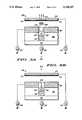
Referring now to FIG. 1A there is depicted a side elevational cross-sectional view of an embodiment of afield emission device 100 in accordance with the present invention. A supportingsubstrate 101 having a major surface is provided. A selectively shaped diamondsemiconductor electron emitter 102 having amajor surface 130 and anemitting surface 120, for emitting electrons, is disposed on the major surface of supportingsubstrate 101.Electron emitter 102 is selectively shaped, in a first method of realizing the diamond emitters, by initially growing a layer of diamond directly onto the major surface of supportingsubstrate 101 and subsequently selectively etching some of the diamond layer to selectively shape diamondsemiconductor electron emitter 102. Alayer 103 of insulator material is deposited on exposed parts of the major surface of supportingsubstrate 101 and disposed onmajor surface 130 of diamondsemiconductor electron emitter 102. Alayer 104 of conductive/semiconductive material is deposited onlayer 103 and disposed on at least a part ofmajor surface 130 of diamondsemiconductor electron emitter 102.
A junction having adepletion region 110, and a depletion region width associated therewith, is formed at the interface between diamondsemiconductor electron emitter 102 andlayer 104 disposed thereon. Ananode 108 is distally disposed with respect to emittingsurface 120 of diamondsemiconductor electron emitter 102 to collect emitted electrons, depicted byarrows 109. While diamondsemiconductor electron emitter 102, anddevice 100, is illustrated as being generally perpendicular to supportingsubstrate 101, it should be understood thatfield emission device 100 could alternatively be formed, generally as described herein, in a horizontal position on a nonconducting supporting substrate.
FIG. 1A further depicts a first externally providedvoltage source 106 operably coupled tolayer 104 of conductive/semiconductive material.Voltage source 106 provides a variable voltage tolayer 104 which will cause the width ofjunction depletion region 110 to vary correspondingly. This modulation of the width ofjunction depletion region 110 results in modulation of the electrons made available at emittingsurface 120 of diamondsemiconductor electron emitter 102.
A second externally providedvoltage source 107 is operably coupled toanode 108 so that emittedelectrons 109 are collected atanode 108.Voltage source 107 further provides an accelerating electric field in the region betweenanode 108 and emittingsurface 120 of diamondsemiconductor electron emitter 102. This electric field is utilized to remove electrons residing at/near emittingsurface 120 of diamondsemiconductor electron emitter 102 and sweep them into the free-space region betweenanode 108 and emittingsurface 120 of diamondsemiconductor electron emitter 102. In the absence of any accelerating electric field, electrons will not transit the region betweenanode 108 and diamondsemiconductor electron emitter 102.
A third externally providedvoltage source 105 is operably coupled to supportingsubstrate 101. Alternatively, supportingsubstrate 101 may be operably coupled to a ground reference potential corresponding to 0.0 volts in place ofvoltage source 105.
FIG. 1B depictsstructure 100 wherein electrons arrive at emittingsurface 120 of diamondsemiconductor electron emitter 102 by transmitting the bulk of the diamond semiconductor and are subsequently swept away from emittingsurface 120 by any accelerating electric field. However, modulation of the width ofjunction depletion region 110 is shown to effectively control the availability of electrons at emittingsurface 120. By so doing electron emission rates are effectively modulated. Increasing the magnitude of the voltage operably coupled tolayer 104 results in an increase in the width ofjunction depletion region 110. Sincejunction depletion region 110 is substantially void of conduction band electrons and since electrons transiting the bulk of the diamond semiconductor do not traversejunction depletion region 110, it is possible to stop the flow of electrons to emittingsurface 120 by applying a voltage of appropriate magnitude tolayer 104, in which casefield emission device 100 is effectively placed in the OFF mode and electron emission is cut-off. FIG. 1B depicts the width ofjunction depletion region 110 as being so extensive as to effectively traverse the entire width of diamondsemiconductor electron emitter 102.
It is one object of the diamond semiconductor of the present invention to provide a field emission electron device which does not suffer from the breakdown mechanisms inherent in the structures of the prior art wherein very high electric fields must be generated at the electron emitter in order to induce electron emission. The diamond semiconductor material employed for the electron emitter in the present invention exhibits an electron affinity of less than 1.0 electron volts corresponding to one crystallographic plane and an electron affinity of less than 0.0 electron volts corresponding to yet another crystallographic plane. A desired electron affinity is attained by depositing the diamond semiconductor material with emittingsurface 120 lying in the chosen crystallographic plane. As such, much smaller magnitude electric fields may be employed to achieve substantial electron emission than is the case with electron emitters of the prior art. Further, there is no need to provide geometric discontinuities of small radius of curvature as required in prior art embodiments.
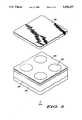
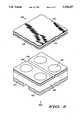
FIG. 2 is a partial perspective view of an embodiment of afield emission device 200 in accordance with the present invention wherein features corresponding to those first described in FIGS. 1A & 1B are similarly referenced beginning with the numeral "2".Device 200 includes a plurality of diamondsemiconductor electron emitters 202 disposed as an array of electron emitters within a single structure. Device operation is essentially similar to that described previously wherein electron emission is substantially controlled by providing a modulating voltage to alayer 204 of conductive/semiconductive material as described previously with reference to FIG. IB. Emitted electrons are collected by ananode 208.
FIG. 3A is a side elevational cross sectional depiction of another embodiment of afield emission device 300 employing a diamondsemiconductor electron emitter 302 in accordance with the present invention and wherein features corresponding to features previously identified with reference to FIGS. 1A & 1B are similarly referenced beginning with the numeral "3". Indevice 300, diamondsemiconductor electron emitter 302 is disposed on afirst layer 315 of conductive/semiconductive material which is selectively patterned subsequent to deposition on the major surface of supportingsubstrate 301. Alternatively, the major surface of supportingsubstrate 301 may be selectively exposed by providing a patterned mask layer, andlayer 315 of conductive/semiconductive material selectively deposited onto the selectively exposed part of the major surface of the supporting substrate. Both techniques are commonly employed in the known art. In this embodiment asecond layer 304 of conductive/semiconductive material corresponds to and performs the same function aslayer 104 of conductive/semiconductive material described previously with reference to FIG. 1A.
FIG. 3A further depicts ananode 308 comprising a plurality of layers including a substantially opticallytransparent faceplate 311 having a surface, a layer ofcathodoluminescent material 312 disposed on the surface offaceplate 311, and aconductive layer 313 disposed oncathodoluminescent layer 312. Emitted electrons, depicted byarrows 309, traversing the region between emitting surface of diamondsemiconductor electron emitter 302 and distally disposedanode 308 imparts energy to active sites withincathodoluminescent layer 312 to stimulate photon emission, depicted byarrows 314, which is observed through substantially opticallytransparent faceplate 311.
FIG. 3B is a side elevational cross-sectional depiction ofdevice 300 functioning as described previously with reference to FIG. 1B. Voltage supplies 305, 306 and 307 are connected and operate as previously described. Indevice 300, electron emission from diamondsemiconductor electron emitter 302 is effectively modulated by applying an appropriate externally provided voltage to layer 304 of conductive/semiconductive material to modulate the width ofjunction depletion region 310. Modulation of electron emission modulates photon emission fromcathodoluminescent layer 312 to produce a visual display.
Referring now to FIG. 4 there is depicted a partial perspective view of adevice 400 wherein features corresponding to features previously identified with reference to FlG. 3A & 3B are similarly referenced beginning with the numeral "4". Indevice 400, a selectively patternedfirst layer 415 of conductive/semiconductive material is realized as a plurality of electrically independent stripes. Similarly in device 400 asecond layer 404 of conductive/semiconductive material is selectively patterned as a plurality of stripes. It should be understood that the term strips is herein defined to encompass any shapes utilized for specific applications, including but not limited to regions or areas, in which layers 415 and 404 are constructed with electrically separate portions. So formed, each of a plurality of diamondsemiconductor electron emitters 402 are selectively placed in the ON/OFF mode and electron emission controlled through provision of selecting the voltage applied to each of the electrically independent stripes. By so doing selected regions of acathodoluminescent layer 412 are induced to emit photons resulting in the formation of an image observable through a substantially opticallytransparent faceplate 411.
Referring now to FIG. 5 there is depicted a partial perspective view of adevice 500 wherein features corresponding to features previously identified with reference to FIG. 4 are similarly referenced beginning with the numeral "5".Device 500, further depicts ananode 508 comprising a plurality of layers including a substantially opticallytransparent faceplate 511 having a surface, aconductive layer 513 disposed on the surface offaceplate 511, and a layer ofcathodoluminescent material 512 disposed onconductive layer 513. It will of course be understood that in this specific embodimentconductive layer 513 is formed of substantially optically transparent material so that photons emitted bycathodoluminescent layer 512 are observable throughfaceplate 511 andconductive layer 513.
Thus, improved electron emitters are disclosed which include diamond semiconductor material for the electron emitter, which exhibits an electron affinity of less than 1.0 electron volts corresponding to one crystallographic plane and an electron affinity of less than 0.0 electron volts corresponding to yet another crystallographic plane. As such, much smaller magnitude electric fields may be employed to achieve substantial electron emission than is the case with electron emitters of the prior art. Because of this reduced electron affinity the electron emitters are not limited to geometric formations, such as tips/edges of small radius of curvature, that incur damage as a result of ion bombardment. Further, in the presence of very low residual gas pressures the emitters are not subjected to ion attack which damages the emitting tip/edge and renders it useless.
While we have shown and described specific embodiments of the present invention, further modifications and improvements will occur to those skilled in the art. We desire it to be understood, therefore, that this invention is not limited to the particular forms shown and we intend in the append claims to cover all modifications that do not depart from the spirit and scope of this invention.
Claims (50)
1. An electrically modulatable electron emitter comprising:
a diamond semiconductor electron emitter having an emitting surface for emitting electrons and a major surface; and
a layer of conductive/semiconductive material disposed at least partially on the major surface of the diamond semiconductor electron emitter and forming a junction depletion region therewith.
2. The electron emitter of claim 1 wherein the diamond semiconductor electron emitter is disposed on a supporting substrate.
3. The electron emitter of claim 1 wherein at least a part of the emitting surface exhibits an electron affinity of less than 1 electron volt.
4. The electron emitter of claim 1 wherein at least a part of the emitting surface exhibits an electron affinity of less than zero volts.
5. An electrically modulatable electron emitter comprising:
a diamond semiconductor electron emitter having a bulk of diamond semiconductor material with an emitting surface for emitting electrons and a major surface;
a layer of conductive/semiconductive material at least partially disposed on the major surface of the diamond semiconductor electron emitter such that a junction having a depletion region, and a depletion region width associated therewith, is formed at the interface corresponding thereto; and
a voltage source operably coupled to the layer of conductive/semiconductive material, such that modulation of the voltage source causes modulation of the junction depletion region width and effectively controls electrons transiting the bulk of the diamond semiconductor material to the emitting surface.
6. The electron emitter of claim 5 wherein the diamond semiconductor electron emitter is disposed on a supporting substrate.
7. The electron emitter of claim 5 wherein at least a part of the emitting surface exhibits an electron affinity of less than 1 electron volt.
8. The electron emitter of claim 5 wherein at least a part of the emitting surface exhibits an electron affinity of less than zero volts.
9. A field emission device comprising:
a supporting substrate having a major surface;
a selectively shaped diamond semiconductor electron emitter having a major surface and an emitting surface, the diamond semiconductor electron emitter being disposed on the major surface of the supporting substrate;
a layer of insulator material disposed on the major surface of the supporting substrate and on a part of the major surface of the diamond semiconductor electron emitter; and
a layer of conductive/semiconductive material disposed on the layer of insulator material and in physical contact with a part of the major surface of the diamond semiconductor electron emitter, such that a junction having a depletion region, and a depletion region width associated therewith, is formed at the interface corresponding thereto.
10. The field emission device of claim 9 and further comprising a plurality of selectively shaped diamond semiconductor electron emitters.
11. The field emission device of claim 9 wherein the layer of conductive/semiconductive material is selectively formed as a plurality of electrically independent stripes.
12. The field emission device of claim 9 wherein at least a part of the emitting surface of the electron emitter exhibits an electron affinity of less than 1 electron volt.
13. The field emission device of claim 9 wherein at least a part of the emitting surface of the electron emitter exhibits an electron affinity of less than zero volts.
14. A field emission device comprising:
a supporting substrate having a major surface;
a first layer of selectively patterned conductive/semiconductive material disposed on the major surface of the supporting substrate;
a selectively shaped diamond semiconductor electron emitter having a major surface and an emitting surface, the diamond semiconductor electron emitter being disposed on the first layer of selectively patterned conductive/semiconductive material;
a layer of insulator material disposed on the major surface of the supporting substrate and at least a part of the major surface of the diamond semiconductor electron emitter; and
a second layer of conductive/semiconductive material disposed on the layer of insulator material and in physical contact with the major surface of the diamond semiconductor electron emitter, such that a junction having a depletion region and having a depletion region width associated therewith is formed at the interface between the layer of conductive/semiconductive material and the diamond semiconductor electron emitter major surface.
15. The field emission device of claim 14 wherein the first layer of conductive/semiconductive material is selectively formed as a plurality of electrically independent stripes.
16. The field emission device of claim 14 wherein the second layer of conductive/semiconductive material is selectively formed as a plurality of electrically independent stripes.
17. The field emission device of claim 14 wherein at least a part of the emitting surface of the diamond semiconductor electron emitter exhibits an electron affinity of less than 1 electron volt.
18. The field emission device of claim 14 wherein at least a part of the emitting surface of the diamond semiconductor electron emitter exhibits an electron affinity of less than zero volts.
19. A field emission device comprising:
a supporting substrate having a major surface;
a first layer of selectively patterned conductive/semiconductive material disposed on the major surface of the supporting substrate;
a first selectively shaped diamond semiconductor electron emitter having a major surface and an emitting surface, the diamond shaped semiconductor electron emitter being disposed on the first layer of selectively patterned conductive/semiconductive material;
a layer of insulator material disposed on the major surface of the supporting substrate and a part of the major surface of the diamond semiconductor electron emitter;
a second layer of conductive/semiconductive material disposed on the layer of insulator material and in physical contact with the major surface of the diamond semiconductor electron emitter such that a junction having a depletion region, and a depletion region width associated therewith, is formed at the interface corresponding thereto; and
an anode distally disposed with respect to the emitting surface of the diamond semiconductor electron emitter for collecting emitted electrons.
20. The field emission device of claim 19 wherein the first layer of conductive/semiconductive material is selectively formed as a plurality of electrically independent stripes.
21. The field emission device of claim 19 wherein the second layer of conductive/semiconductive material is selectively formed as a plurality of electrically independent stripes.
22. The field emission device of claim 19 wherein at least a part of the emitting surface of the diamond semiconductor electron emitter exhibits an electron affinity of less than 1 electron volt.
23. The field emission device of claim 19 wherein at least a part of the emitting surface of the diamond semiconductor electron emitter exhibits an electron affinity of less than zero volts.
24. The field emission device of claim 19 wherein the anode electrode includes
a substantially optically transparent faceplate having a surface,
a layer of cathodoluminescent material disposed on the surface of the faceplate, and
a conductive layer disposed on the layer of cathodoluminescent material.
25. The field emission device of claim 19 wherein the anode electrode includes
a substantially optically transparent faceplate having a surface,
a conductive layer disposed on the surface of the faceplate, and
a layer of cathodoluminescent material disposed on the conductive layer.
26. A field emission device comprising:
a supporting substrate having a major surface;
a first selectively shaped diamond semiconductor electron emitter having a major surface and an emitting surface, the diamond semiconductor electron emitter being disposed on the major surface of the supporting substrate;
a layer of insulator material disposed on the major surface of the supporting substrate and a part of the major surface of the diamond semiconductor electron emitter;
a layer of conductive/semiconductive material disposed on the layer of insulator material and in physical contact with the major surface of the diamond semiconductor electron emitter such that a junction having a depletion region, and having an associated depletion region width, is formed at the interface between the layer of conductive/semiconductive material and the diamond semiconductor electron emitter major surface; and
an anode distally disposed with respect to the emitting surface of the diamond semiconductor electron emitter for collecting emitted electrons.
27. The field emission device of claim 26 wherein the anode electrode includes
a substantially optically transparent faceplate having a surface,
a layer of cathodoluminescent material disposed on the surface of the faceplate, and
a conductive layer disposed on the layer of cathodoluminescent material.
28. The field emission device of claim 26 wherein at least a part of the emitting surface of the diamond semiconductor electron emitter exhibits an electron affinity of less than 1 electron volt.
29. The electron emitter of claim 26 wherein at least a part of the emitting surface of the diamond semiconductor electron emitter exhibits an electron affinity of less than zero volts.
30. A field emission device comprising:
a supporting substrate having a major surface; electron emitter having a bulk with a major surface and an emitting surface, the diamond semiconductor electron emitter being disposed on a part of the major surface of the supporting substrate;
a layer of insulator material disposed on the major surface of the supporting substrate and a part of the major surface of the diamond semiconductor electron emitter;
a layer of conductive/semiconductive material disposed on the layer of insulator material and in physical contact with the major surface of the diamond semiconductor electron emitter such that a junction having a depletion region, and having a depletion region width associated therewith, is formed at the interface between the layer of conductive/semiconductive material and the diamond semiconductor electron emitter major surface and extending into the bulk of the diamond semiconductor electron emitter; and
a first externally provided voltage source operably coupled to the layer of conductive/semiconductive material and modulating the width of the junction depletion region, such that modulation of the junction width effectively controls the availability of electrons at the emitting surface of the diamond semiconductor electron emitter.
31. The field emission device of claim 30 wherein at least a part of the emitting surface of the diamond semiconductor electron emitter exhibits an electron affinity of less than 1 electron volt.
32. The field emission device of claim 30 wherein at least a part of the emitting surface of the diamond semiconductor electron emitter exhibits an electron affinity of less than zero volts.
33. A field emission device comprising:
a supporting substrate having a major surface;
a first selectively shaped diamond semiconductor electron emitter having a bulk with a major surface and an emitting surface, the diamond semiconductor electron emitter being disposed on a part of the major surface of the supporting substrate;
a layer of insulator material disposed on the major surface of the supporting substrate and a part of the major surface of the diamond semiconductor electron emitter;
a layer of conductive/semiconductive material disposed on the layer of insulator material and in physical contact with the major surface of the diamond semiconductor electron emitter such that a junction having a depletion region, and having a depletion region width associated therewith, is formed at the interface between the layer of conductive/semiconductive material and the diamond semiconductor electron emitter major surface and extending into the bulk of the diamond semiconductor electron emitter;
a voltage source operably coupled to the layer of conductive/semiconductive material for modulating the width of the junction depletion region; and
an anode for collecting electrons emitted from the diamond semiconductor electron emitter emitting surface, such that modulation of the junction width effectively controls the availability of electrons at the emitting surface of the diamond semiconductor electron emitter.
34. The field emission device of claim 33 wherein the anode electrode includes
a substantially optically transparent faceplate having a surface, and
a layer of cathodoluminescent material disposed on the surface of the faceplate, and
a conductive layer disposed on the layer of cathodoluminescent material.
35. The field emission device of claim 33 wherein the anode electrode includes
a substantially optically transparent faceplate having a surface,
a conductive layer disposed on the surface of the faceplate, and
a layer of cathodoluminescent material disposed on the conductive layer.
36. The field emission device of claim 33 wherein at least a part of the emitting surface of the diamond semiconductor electron emitter exhibits an electron affinity of less than 1 electron volt.
37. The field emission device of claim 33 wherein at least a part of the emitting surface of the diamond semiconductor electron emitter exhibits an electron affinity of less than zero volts.
38. A field emission device comprising:
a supporting substrate having a major surface;
a first layer of selectively patterned conductive/semiconductive material disposed on the major surface of the supporting substrate;
a selectively shaped diamond semiconductor electron emitter having a major surface and an emitting surface, the diamond semiconductor electron emitter being disposed on the first layer of selectively patterned conductive/semiconductive material;
a layer of insulator material disposed on the major surface of the supporting substrate and a part of the major surface of the diamond semiconductor electron emitter;
a second layer of conductive/semiconductive material disposed on the layer of insulator material and in physical contact with the major surface of the diamond semiconductor electron emitter such that a junction having a depletion region, and a depletion region width associated therewith, is formed at the interface corresponding thereto;
a voltage source operably coupled to the second layer of conductive/semiconductive material for modulating the width of the junction depletion region; and
an anode for collecting electrons emitted from the emitting surface of the diamond semiconductor electron emitter, such that modulation of the junction width effectively controls the availability of electrons at the emitting surface of the diamond semiconductor electron emitter.
39. The field emission device of claim 38 wherein the first layer of conductive/semiconductive material is selectively formed as a plurality of electrically independent stripes.
40. The field emission device of claim 38 wherein the second layer of conductive/semiconductive material is selectively formed as a plurality of electrically independent stripes.
41. The field emission device of claim 38 wherein the anode electrode includes
a substantially optically transparent faceplate having a surface,
a layer of cathodoluminescent material disposed on the surface of the faceplate, and
a conductive layer disposed on the layer of cathodoluminescent material.
42. The field emission device of claim 38 wherein the anode electrode includes
a substantially optically transparent faceplate having a surface,
a conductive layer disposed on the surface of the faceplate, and
a layer of cathodoluminescent material disposed on the conductive layer.
43. The field emission device of claim 38 wherein at least a part of the emitting surface of the diamond semiconductor electron emitter exhibits an electron affinity of less than 1 electron volt.
44. The field emission device of claim 38 wherein at least a part of the emitting surface of the diamond semiconductor electron emitter exhibits an electron affinity of less than zero volts.
45. A method of producing an electrically modulatable electron emitter comprising the steps of:
forming a diamond semiconductor electron emitter with an emitting surface for emitting electrons and a major surface; and
forming a layer of conductive/semiconductive material in contact with the major surface of the diamond semiconductor electron emitter such that an electron depletion region, and a depletion region width associated therewith, is formed at an interface between the diamond semiconductor electron emitter and the layer of conductive/semiconductive material.
46. A method of producing an electrically modulatable electron emitter as set forth in claim 45 including in addition the step of coupling a voltage source to the layer of conductive/semiconductive material, such that modulation of the voltage source causes modulation of the depletion region width and effectively controls electrons transiting the bulk of the diamond semiconductor material to the emitting surface.
47. A method of producing a field emission device comprising the steps of:
forming a selectively shaped diamond semiconductor electron emitter with a major surface and an emitting surface;
forming a layer of conductive/semiconductive material in physical contact with the major surface of the diamond semiconductor electron emitter such that a junction having a depletion region, and a depletion region width associated therewith, is formed at an interface between the diamond semiconductor electron emitter and the layer of conductive/semiconductive material; and
forming an anode distally disposed with respect to the emitting surface of the diamond semiconductor electron emitter for collecting emitted electrons from the emitting surface of the diamond semiconductor electron emitter, such that modulation of the junction width effectively controls the availability of electrons at the emitting surface of the diamond semiconductor electron emitter.
48. A method of producing a field emission device as claimed in claim 47 including in addition the step of coupling a voltage source to the layer of conductive/semiconductive material for modulating the width of the junction depletion region.
49. A method of producing a field emission device as claimed in claim 47 wherein the step of forming the anode includes
forming a substantially optically transparent faceplate having a surface,
disposing a layer of cathodoluminescent material on the surface of the faceplate, and
disposing a conductive layer on the layer of cathodoluminescent material.
50. A method of producing a field emission device as claimed in claim 47 wherein the step of forming the anode includes
forming a substantially optically transparent faceplate having a surface,
disposing a conductive layer on the surface of the faceplate, and
disposing a layer of cathodoluminescent material on the conductive layer.
Priority Applications (5)
| Application Number | Priority Date | Filing Date | Title |
|---|---|---|---|
| US07/747,564US5138237A (en) | 1991-08-20 | 1991-08-20 | Field emission electron device employing a modulatable diamond semiconductor emitter |
| CA002070942ACA2070942A1 (en) | 1991-08-20 | 1992-06-10 | Field emission electron device employing a modulatable diamond semiconductor emitter |
| CN 92105455CN1069825A (en) | 1991-08-20 | 1992-07-06 | Adopt the field emission electron device of adjustable diamond semiconductor emitter |
| EP92113952AEP0528390A1 (en) | 1991-08-20 | 1992-08-17 | A field emission electron device employing a modulatable diamond semiconductor emitter |
| JP24000192AJPH05205612A (en) | 1991-08-20 | 1992-08-17 | Field emission electronic device and manufacture thereof |
Applications Claiming Priority (1)
| Application Number | Priority Date | Filing Date | Title |
|---|---|---|---|
| US07/747,564US5138237A (en) | 1991-08-20 | 1991-08-20 | Field emission electron device employing a modulatable diamond semiconductor emitter |
Publications (1)
| Publication Number | Publication Date |
|---|---|
| US5138237Atrue US5138237A (en) | 1992-08-11 |
Family
ID=25005652
Family Applications (1)
| Application Number | Title | Priority Date | Filing Date |
|---|---|---|---|
| US07/747,564Expired - Fee RelatedUS5138237A (en) | 1991-08-20 | 1991-08-20 | Field emission electron device employing a modulatable diamond semiconductor emitter |
Country Status (5)
| Country | Link |
|---|---|
| US (1) | US5138237A (en) |
| EP (1) | EP0528390A1 (en) |
| JP (1) | JPH05205612A (en) |
| CN (1) | CN1069825A (en) |
| CA (1) | CA2070942A1 (en) |
Cited By (76)
| Publication number | Priority date | Publication date | Assignee | Title |
|---|---|---|---|---|
| US5278475A (en)* | 1992-06-01 | 1994-01-11 | Motorola, Inc. | Cathodoluminescent display apparatus and method for realization using diamond crystallites |
| US5289086A (en)* | 1992-05-04 | 1994-02-22 | Motorola, Inc. | Electron device employing a diamond film electron source |
| US5340997A (en)* | 1993-09-20 | 1994-08-23 | Hewlett-Packard Company | Electrostatically shielded field emission microelectronic device |
| US5341063A (en)* | 1991-11-07 | 1994-08-23 | Microelectronics And Computer Technology Corporation | Field emitter with diamond emission tips |
| WO1995012835A1 (en)* | 1993-11-04 | 1995-05-11 | Microelectronics And Computer Technology Corporation | Methods for fabricating flat panel display systems and components |
| US5430348A (en)* | 1992-06-01 | 1995-07-04 | Motorola, Inc. | Inversion mode diamond electron source |
| EP0645793A3 (en)* | 1993-09-24 | 1995-09-13 | Sumitomo Electric Industries | Electron device. |
| EP0700066A1 (en) | 1994-08-31 | 1996-03-06 | AT&T Corp. | Spaced-gate emission device and method for making same |
| US5505649A (en)* | 1994-07-27 | 1996-04-09 | Samsung Display Devices Co., Ltd. | Field emission display device and method for producing such display device |
| EP0709870A1 (en) | 1994-10-31 | 1996-05-01 | AT&T Corp. | Methods and apparatus for making enhanced particulate field emitters and resulting products |
| EP0709869A1 (en) | 1994-10-31 | 1996-05-01 | AT&T Corp. | Field emission devices employing enhanced diamond field emitters |
| US5531880A (en)* | 1994-09-13 | 1996-07-02 | Microelectronics And Computer Technology Corporation | Method for producing thin, uniform powder phosphor for display screens |
| US5536193A (en)* | 1991-11-07 | 1996-07-16 | Microelectronics And Computer Technology Corporation | Method of making wide band gap field emitter |
| US5545946A (en)* | 1993-12-17 | 1996-08-13 | Motorola | Field emission display with getter in vacuum chamber |
| US5550426A (en)* | 1994-06-30 | 1996-08-27 | Motorola | Field emission device |
| US5551903A (en)* | 1992-03-16 | 1996-09-03 | Microelectronics And Computer Technology | Flat panel display based on diamond thin films |
| US5561340A (en)* | 1995-01-31 | 1996-10-01 | Lucent Technologies Inc. | Field emission display having corrugated support pillars and method for manufacturing |
| US5578901A (en)* | 1994-02-14 | 1996-11-26 | E. I. Du Pont De Nemours And Company | Diamond fiber field emitters |
| US5580380A (en)* | 1991-12-20 | 1996-12-03 | North Carolina State University | Method for forming a diamond coated field emitter and device produced thereby |
| WO1996038853A1 (en)* | 1995-06-01 | 1996-12-05 | Microelectronics And Computer Technology Corporation | A field emission display device |
| US5588894A (en)* | 1994-08-31 | 1996-12-31 | Lucent Technologies Inc. | Field emission device and method for making same |
| US5592053A (en)* | 1994-12-06 | 1997-01-07 | Kobe Steel Usa, Inc. | Diamond target electron beam device |
| US5598056A (en)* | 1995-01-31 | 1997-01-28 | Lucent Technologies Inc. | Multilayer pillar structure for improved field emission devices |
| US5600200A (en) | 1992-03-16 | 1997-02-04 | Microelectronics And Computer Technology Corporation | Wire-mesh cathode |
| US5602439A (en)* | 1994-02-14 | 1997-02-11 | The Regents Of The University Of California, Office Of Technology Transfer | Diamond-graphite field emitters |
| US5612712A (en) | 1992-03-16 | 1997-03-18 | Microelectronics And Computer Technology Corporation | Diode structure flat panel display |
| US5616368A (en)* | 1995-01-31 | 1997-04-01 | Lucent Technologies Inc. | Field emission devices employing activated diamond particle emitters and methods for making same |
| US5628659A (en)* | 1995-04-24 | 1997-05-13 | Microelectronics And Computer Corporation | Method of making a field emission electron source with random micro-tip structures |
| EP0773574A1 (en) | 1995-11-09 | 1997-05-14 | AT&T Corp. | Field emission devices employing emitters on metal foil and methods for making such devices |
| US5631196A (en)* | 1994-07-18 | 1997-05-20 | Motorola | Method for making inversion mode diamond electron source |
| US5647998A (en)* | 1995-06-13 | 1997-07-15 | Advanced Vision Technologies, Inc. | Fabrication process for laminar composite lateral field-emission cathode |
| US5675216A (en) | 1992-03-16 | 1997-10-07 | Microelectronics And Computer Technololgy Corp. | Amorphic diamond film flat field emission cathode |
| US5679895A (en)* | 1995-05-01 | 1997-10-21 | Kobe Steel Usa, Inc. | Diamond field emission acceleration sensor |
| US5679043A (en) | 1992-03-16 | 1997-10-21 | Microelectronics And Computer Technology Corporation | Method of making a field emitter |
| US5703380A (en)* | 1995-06-13 | 1997-12-30 | Advanced Vision Technologies Inc. | Laminar composite lateral field-emission cathode |
| US5710478A (en)* | 1995-08-25 | 1998-01-20 | Agency Of Industrial Science & Technology, Ministry Of International Trade & Industry | Field emitter having source, channel, and drain layers |
| US5709577A (en)* | 1994-12-22 | 1998-01-20 | Lucent Technologies Inc. | Method of making field emission devices employing ultra-fine diamond particle emitters |
| US5747918A (en)* | 1994-03-30 | 1998-05-05 | Lucent Technologies Inc. | Display apparatus comprising diamond field emitters |
| US5747815A (en)* | 1993-09-22 | 1998-05-05 | Northrop Grumman Corporation | Micro-miniature ionizer for gas sensor applications and method of making micro-miniature ionizer |
| US5751262A (en)* | 1995-01-24 | 1998-05-12 | Micron Display Technology, Inc. | Method and apparatus for testing emissive cathodes |
| US5757344A (en)* | 1991-09-30 | 1998-05-26 | Kabushiki Kaisha Kobe Seiko Sho | Cold cathode emitter element |
| WO1998044529A1 (en)* | 1996-06-25 | 1998-10-08 | Vanderbilt University | Microtip vacuum field emitter structures, arrays, and devices, and methods of fabrication |
| US5844252A (en)* | 1993-09-24 | 1998-12-01 | Sumitomo Electric Industries, Ltd. | Field emission devices having diamond field emitter, methods for making same, and methods for fabricating porous diamond |
| US5888113A (en)* | 1997-03-27 | 1999-03-30 | Universities Research Association, Inc. | Process for making a cesiated diamond film field emitter and field emitter formed therefrom |
| US5892231A (en)* | 1997-02-05 | 1999-04-06 | Lockheed Martin Energy Research Corporation | Virtual mask digital electron beam lithography |
| US5916005A (en)* | 1996-02-01 | 1999-06-29 | Korea Institute Of Science And Technology | High curvature diamond field emitter tip fabrication method |
| US5965971A (en)* | 1993-01-19 | 1999-10-12 | Kypwee Display Corporation | Edge emitter display device |
| US6020677A (en)* | 1996-11-13 | 2000-02-01 | E. I. Du Pont De Nemours And Company | Carbon cone and carbon whisker field emitters |
| US6060839A (en)* | 1995-08-09 | 2000-05-09 | Thermotrex Corporation | Thin diamond electron beam amplifier |
| EP0971386A3 (en)* | 1992-12-23 | 2000-05-17 | SI Diamond Technology, Inc. | Triode structure flat panel display employing flat field emission cathodes |
| WO2000033351A1 (en)* | 1998-11-30 | 2000-06-08 | Koninklijke Philips Electronics N.V. | Discharge lamp |
| US6127773A (en) | 1992-03-16 | 2000-10-03 | Si Diamond Technology, Inc. | Amorphic diamond film flat field emission cathode |
| US6181055B1 (en) | 1998-10-12 | 2001-01-30 | Extreme Devices, Inc. | Multilayer carbon-based field emission electron device for high current density applications |
| US6204834B1 (en) | 1994-08-17 | 2001-03-20 | Si Diamond Technology, Inc. | System and method for achieving uniform screen brightness within a matrix display |
| US6250984B1 (en) | 1999-01-25 | 2001-06-26 | Agere Systems Guardian Corp. | Article comprising enhanced nanotube emitter structure and process for fabricating article |
| US6283812B1 (en) | 1999-01-25 | 2001-09-04 | Agere Systems Guardian Corp. | Process for fabricating article comprising aligned truncated carbon nanotubes |
| US6296740B1 (en) | 1995-04-24 | 2001-10-02 | Si Diamond Technology, Inc. | Pretreatment process for a surface texturing process |
| US6351254B2 (en)* | 1998-07-06 | 2002-02-26 | The Regents Of The University Of California | Junction-based field emission structure for field emission display |
| US6441550B1 (en) | 1998-10-12 | 2002-08-27 | Extreme Devices Inc. | Carbon-based field emission electron device for high current density applications |
| US6498349B1 (en) | 1997-02-05 | 2002-12-24 | Ut-Battelle | Electrostatically focused addressable field emission array chips (AFEA's) for high-speed massively parallel maskless digital E-beam direct write lithography and scanning electron microscopy |
| US6553096B1 (en) | 2000-10-06 | 2003-04-22 | The University Of North Carolina Chapel Hill | X-ray generating mechanism using electron field emission cathode |
| US6630772B1 (en) | 1998-09-21 | 2003-10-07 | Agere Systems Inc. | Device comprising carbon nanotube field emitter structure and process for forming device |
| US20040028183A1 (en)* | 2000-10-06 | 2004-02-12 | Jianping Lu | Method and apparatus for controlling electron beam current |
| US6741019B1 (en) | 1999-10-18 | 2004-05-25 | Agere Systems, Inc. | Article comprising aligned nanowires |
| US20050226361A1 (en)* | 2000-10-06 | 2005-10-13 | The University Of North Carolina At Chapel Hill | Computed tomography scanning system and method using a field emission x-ray source |
| US20060008047A1 (en)* | 2000-10-06 | 2006-01-12 | The University Of North Carolina At Chapel Hill | Computed tomography system for imaging of human and small animal |
| US20060018432A1 (en)* | 2000-10-06 | 2006-01-26 | The University Of North Carolina At Chapel Hill | Large-area individually addressable multi-beam x-ray system and method of forming same |
| US20080069420A1 (en)* | 2006-05-19 | 2008-03-20 | Jian Zhang | Methods, systems, and computer porgram products for binary multiplexing x-ray radiography |
| US20090022264A1 (en)* | 2007-07-19 | 2009-01-22 | Zhou Otto Z | Stationary x-ray digital breast tomosynthesis systems and related methods |
| US20100239064A1 (en)* | 2005-04-25 | 2010-09-23 | Unc-Chapel Hill | Methods, systems, and computer program products for multiplexing computed tomography |
| US20100329413A1 (en)* | 2009-01-16 | 2010-12-30 | Zhou Otto Z | Compact microbeam radiation therapy systems and methods for cancer treatment and research |
| RU2446506C1 (en)* | 2010-07-12 | 2012-03-27 | Борис Исаакович Горфинкель | Cell with field emission and method of its production |
| US8358739B2 (en) | 2010-09-03 | 2013-01-22 | The University Of North Carolina At Chapel Hill | Systems and methods for temporal multiplexing X-ray imaging |
| US9782136B2 (en) | 2014-06-17 | 2017-10-10 | The University Of North Carolina At Chapel Hill | Intraoral tomosynthesis systems, methods, and computer readable media for dental imaging |
| US10835199B2 (en) | 2016-02-01 | 2020-11-17 | The University Of North Carolina At Chapel Hill | Optical geometry calibration devices, systems, and related methods for three dimensional x-ray imaging |
| US10980494B2 (en) | 2014-10-20 | 2021-04-20 | The University Of North Carolina At Chapel Hill | Systems and related methods for stationary digital chest tomosynthesis (s-DCT) imaging |
Families Citing this family (2)
| Publication number | Priority date | Publication date | Assignee | Title |
|---|---|---|---|---|
| JP3026484B2 (en)* | 1996-08-23 | 2000-03-27 | 日本電気株式会社 | Field emission cold cathode |
| CN1652283B (en)* | 2005-01-01 | 2011-01-12 | 中国海洋大学 | A field emission electron source device and its preparation method |
Citations (13)
| Publication number | Priority date | Publication date | Assignee | Title |
|---|---|---|---|---|
| US3921022A (en)* | 1974-09-03 | 1975-11-18 | Rca Corp | Field emitting device and method of making same |
| US3970887A (en)* | 1974-06-19 | 1976-07-20 | Micro-Bit Corporation | Micro-structure field emission electron source |
| US3998678A (en)* | 1973-03-22 | 1976-12-21 | Hitachi, Ltd. | Method of manufacturing thin-film field-emission electron source |
| US4008412A (en)* | 1974-08-16 | 1977-02-15 | Hitachi, Ltd. | Thin-film field-emission electron source and a method for manufacturing the same |
| US4084942A (en)* | 1975-08-27 | 1978-04-18 | Villalobos Humberto Fernandez | Ultrasharp diamond edges and points and method of making |
| US4095133A (en)* | 1976-04-29 | 1978-06-13 | U.S. Philips Corporation | Field emission device |
| US4513308A (en)* | 1982-09-23 | 1985-04-23 | The United States Of America As Represented By The Secretary Of The Navy | p-n Junction controlled field emitter array cathode |
| US4780684A (en)* | 1987-10-22 | 1988-10-25 | Hughes Aircraft Company | Microwave integrated distributed amplifier with field emission triodes |
| JPH0260024A (en)* | 1988-08-24 | 1990-02-28 | Canon Inc | electron-emitting device |
| JPH0296532A (en)* | 1988-10-03 | 1990-04-09 | Akiomi Yamaguchi | Liver disease treatment consisting of a water-soluble extract from a plant of the Tiberaceae family. |
| US4990766A (en)* | 1989-05-22 | 1991-02-05 | Murasa International | Solid state electron amplifier |
| US5053673A (en)* | 1988-10-17 | 1991-10-01 | Matsushita Electric Industrial Co., Ltd. | Field emission cathodes and method of manufacture thereof |
| US5064396A (en)* | 1990-01-29 | 1991-11-12 | Coloray Display Corporation | Method of manufacturing an electric field producing structure including a field emission cathode |
Family Cites Families (2)
| Publication number | Priority date | Publication date | Assignee | Title |
|---|---|---|---|---|
| JPH0275902A (en)* | 1988-09-13 | 1990-03-15 | Seiko Instr Inc | Diamond probe and its forming method |
| US5007873A (en)* | 1990-02-09 | 1991-04-16 | Motorola, Inc. | Non-planar field emission device having an emitter formed with a substantially normal vapor deposition process |
- 1991
- 1991-08-20USUS07/747,564patent/US5138237A/ennot_activeExpired - Fee Related
- 1992
- 1992-06-10CACA002070942Apatent/CA2070942A1/ennot_activeAbandoned
- 1992-07-06CNCN 92105455patent/CN1069825A/enactivePending
- 1992-08-17JPJP24000192Apatent/JPH05205612A/enactivePending
- 1992-08-17EPEP92113952Apatent/EP0528390A1/ennot_activeWithdrawn
Patent Citations (13)
| Publication number | Priority date | Publication date | Assignee | Title |
|---|---|---|---|---|
| US3998678A (en)* | 1973-03-22 | 1976-12-21 | Hitachi, Ltd. | Method of manufacturing thin-film field-emission electron source |
| US3970887A (en)* | 1974-06-19 | 1976-07-20 | Micro-Bit Corporation | Micro-structure field emission electron source |
| US4008412A (en)* | 1974-08-16 | 1977-02-15 | Hitachi, Ltd. | Thin-film field-emission electron source and a method for manufacturing the same |
| US3921022A (en)* | 1974-09-03 | 1975-11-18 | Rca Corp | Field emitting device and method of making same |
| US4084942A (en)* | 1975-08-27 | 1978-04-18 | Villalobos Humberto Fernandez | Ultrasharp diamond edges and points and method of making |
| US4095133A (en)* | 1976-04-29 | 1978-06-13 | U.S. Philips Corporation | Field emission device |
| US4513308A (en)* | 1982-09-23 | 1985-04-23 | The United States Of America As Represented By The Secretary Of The Navy | p-n Junction controlled field emitter array cathode |
| US4780684A (en)* | 1987-10-22 | 1988-10-25 | Hughes Aircraft Company | Microwave integrated distributed amplifier with field emission triodes |
| JPH0260024A (en)* | 1988-08-24 | 1990-02-28 | Canon Inc | electron-emitting device |
| JPH0296532A (en)* | 1988-10-03 | 1990-04-09 | Akiomi Yamaguchi | Liver disease treatment consisting of a water-soluble extract from a plant of the Tiberaceae family. |
| US5053673A (en)* | 1988-10-17 | 1991-10-01 | Matsushita Electric Industrial Co., Ltd. | Field emission cathodes and method of manufacture thereof |
| US4990766A (en)* | 1989-05-22 | 1991-02-05 | Murasa International | Solid state electron amplifier |
| US5064396A (en)* | 1990-01-29 | 1991-11-12 | Coloray Display Corporation | Method of manufacturing an electric field producing structure including a field emission cathode |
Cited By (117)
| Publication number | Priority date | Publication date | Assignee | Title |
|---|---|---|---|---|
| US5757344A (en)* | 1991-09-30 | 1998-05-26 | Kabushiki Kaisha Kobe Seiko Sho | Cold cathode emitter element |
| US5536193A (en)* | 1991-11-07 | 1996-07-16 | Microelectronics And Computer Technology Corporation | Method of making wide band gap field emitter |
| US5341063A (en)* | 1991-11-07 | 1994-08-23 | Microelectronics And Computer Technology Corporation | Field emitter with diamond emission tips |
| US5861707A (en) | 1991-11-07 | 1999-01-19 | Si Diamond Technology, Inc. | Field emitter with wide band gap emission areas and method of using |
| US5580380A (en)* | 1991-12-20 | 1996-12-03 | North Carolina State University | Method for forming a diamond coated field emitter and device produced thereby |
| US5686791A (en) | 1992-03-16 | 1997-11-11 | Microelectronics And Computer Technology Corp. | Amorphic diamond film flat field emission cathode |
| US5612712A (en) | 1992-03-16 | 1997-03-18 | Microelectronics And Computer Technology Corporation | Diode structure flat panel display |
| US6127773A (en) | 1992-03-16 | 2000-10-03 | Si Diamond Technology, Inc. | Amorphic diamond film flat field emission cathode |
| US5551903A (en)* | 1992-03-16 | 1996-09-03 | Microelectronics And Computer Technology | Flat panel display based on diamond thin films |
| US5675216A (en) | 1992-03-16 | 1997-10-07 | Microelectronics And Computer Technololgy Corp. | Amorphic diamond film flat field emission cathode |
| US5703435A (en) | 1992-03-16 | 1997-12-30 | Microelectronics & Computer Technology Corp. | Diamond film flat field emission cathode |
| US6629869B1 (en) | 1992-03-16 | 2003-10-07 | Si Diamond Technology, Inc. | Method of making flat panel displays having diamond thin film cathode |
| US5600200A (en) | 1992-03-16 | 1997-02-04 | Microelectronics And Computer Technology Corporation | Wire-mesh cathode |
| US5679043A (en) | 1992-03-16 | 1997-10-21 | Microelectronics And Computer Technology Corporation | Method of making a field emitter |
| US5763997A (en) | 1992-03-16 | 1998-06-09 | Si Diamond Technology, Inc. | Field emission display device |
| US5289086A (en)* | 1992-05-04 | 1994-02-22 | Motorola, Inc. | Electron device employing a diamond film electron source |
| US5430348A (en)* | 1992-06-01 | 1995-07-04 | Motorola, Inc. | Inversion mode diamond electron source |
| US5278475A (en)* | 1992-06-01 | 1994-01-11 | Motorola, Inc. | Cathodoluminescent display apparatus and method for realization using diamond crystallites |
| EP0971386A3 (en)* | 1992-12-23 | 2000-05-17 | SI Diamond Technology, Inc. | Triode structure flat panel display employing flat field emission cathodes |
| US5965971A (en)* | 1993-01-19 | 1999-10-12 | Kypwee Display Corporation | Edge emitter display device |
| US6023126A (en)* | 1993-01-19 | 2000-02-08 | Kypwee Display Corporation | Edge emitter with secondary emission display |
| US5340997A (en)* | 1993-09-20 | 1994-08-23 | Hewlett-Packard Company | Electrostatically shielded field emission microelectronic device |
| US5747815A (en)* | 1993-09-22 | 1998-05-05 | Northrop Grumman Corporation | Micro-miniature ionizer for gas sensor applications and method of making micro-miniature ionizer |
| EP0645793A3 (en)* | 1993-09-24 | 1995-09-13 | Sumitomo Electric Industries | Electron device. |
| US5552613A (en)* | 1993-09-24 | 1996-09-03 | Sumitomo Electric Industries, Ltd. | Electron device |
| US5844252A (en)* | 1993-09-24 | 1998-12-01 | Sumitomo Electric Industries, Ltd. | Field emission devices having diamond field emitter, methods for making same, and methods for fabricating porous diamond |
| US5614353A (en) | 1993-11-04 | 1997-03-25 | Si Diamond Technology, Inc. | Methods for fabricating flat panel display systems and components |
| US5601966A (en) | 1993-11-04 | 1997-02-11 | Microelectronics And Computer Technology Corporation | Methods for fabricating flat panel display systems and components |
| RU2141698C1 (en)* | 1993-11-04 | 1999-11-20 | Микроэлектроникс энд Компьютер Текнолоджи Корпорейшн | Process of manufacture of systems of display with planar screen and of their components |
| WO1995012835A1 (en)* | 1993-11-04 | 1995-05-11 | Microelectronics And Computer Technology Corporation | Methods for fabricating flat panel display systems and components |
| US5652083A (en) | 1993-11-04 | 1997-07-29 | Microelectronics And Computer Technology Corporation | Methods for fabricating flat panel display systems and components |
| US5545946A (en)* | 1993-12-17 | 1996-08-13 | Motorola | Field emission display with getter in vacuum chamber |
| US5602439A (en)* | 1994-02-14 | 1997-02-11 | The Regents Of The University Of California, Office Of Technology Transfer | Diamond-graphite field emitters |
| US5578901A (en)* | 1994-02-14 | 1996-11-26 | E. I. Du Pont De Nemours And Company | Diamond fiber field emitters |
| US5747918A (en)* | 1994-03-30 | 1998-05-05 | Lucent Technologies Inc. | Display apparatus comprising diamond field emitters |
| US5550426A (en)* | 1994-06-30 | 1996-08-27 | Motorola | Field emission device |
| US5631196A (en)* | 1994-07-18 | 1997-05-20 | Motorola | Method for making inversion mode diamond electron source |
| US5505649A (en)* | 1994-07-27 | 1996-04-09 | Samsung Display Devices Co., Ltd. | Field emission display device and method for producing such display device |
| US6204834B1 (en) | 1994-08-17 | 2001-03-20 | Si Diamond Technology, Inc. | System and method for achieving uniform screen brightness within a matrix display |
| US5698934A (en)* | 1994-08-31 | 1997-12-16 | Lucent Technologies Inc. | Field emission device with randomly distributed gate apertures |
| US5588894A (en)* | 1994-08-31 | 1996-12-31 | Lucent Technologies Inc. | Field emission device and method for making same |
| US5681196A (en)* | 1994-08-31 | 1997-10-28 | Lucent Technologies Inc. | Spaced-gate emission device and method for making same |
| US5808401A (en)* | 1994-08-31 | 1998-09-15 | Lucent Technologies Inc. | Flat panel display device |
| US5504385A (en)* | 1994-08-31 | 1996-04-02 | At&T Corp. | Spaced-gate emission device and method for making same |
| EP0700066A1 (en) | 1994-08-31 | 1996-03-06 | AT&T Corp. | Spaced-gate emission device and method for making same |
| US5531880A (en)* | 1994-09-13 | 1996-07-02 | Microelectronics And Computer Technology Corporation | Method for producing thin, uniform powder phosphor for display screens |
| US5811916A (en)* | 1994-10-31 | 1998-09-22 | Lucent Technologies Inc. | Field emission devices employing enhanced diamond field emitters |
| EP0709870A1 (en) | 1994-10-31 | 1996-05-01 | AT&T Corp. | Methods and apparatus for making enhanced particulate field emitters and resulting products |
| EP0709869A1 (en) | 1994-10-31 | 1996-05-01 | AT&T Corp. | Field emission devices employing enhanced diamond field emitters |
| US5637950A (en)* | 1994-10-31 | 1997-06-10 | Lucent Technologies Inc. | Field emission devices employing enhanced diamond field emitters |
| US5623180A (en)* | 1994-10-31 | 1997-04-22 | Lucent Technologies Inc. | Electron field emitters comprising particles cooled with low voltage emitting material |
| US5592053A (en)* | 1994-12-06 | 1997-01-07 | Kobe Steel Usa, Inc. | Diamond target electron beam device |
| US5977697A (en)* | 1994-12-22 | 1999-11-02 | Lucent Technologies Inc. | Field emission devices employing diamond particle emitters |
| US5709577A (en)* | 1994-12-22 | 1998-01-20 | Lucent Technologies Inc. | Method of making field emission devices employing ultra-fine diamond particle emitters |
| US5751262A (en)* | 1995-01-24 | 1998-05-12 | Micron Display Technology, Inc. | Method and apparatus for testing emissive cathodes |
| US6429835B1 (en) | 1995-01-24 | 2002-08-06 | Micron Technologies, Inc. | Method and apparatus for testing emissive cathodes |
| US5561340A (en)* | 1995-01-31 | 1996-10-01 | Lucent Technologies Inc. | Field emission display having corrugated support pillars and method for manufacturing |
| US5616368A (en)* | 1995-01-31 | 1997-04-01 | Lucent Technologies Inc. | Field emission devices employing activated diamond particle emitters and methods for making same |
| US5690530A (en)* | 1995-01-31 | 1997-11-25 | Lucent Technologies Inc. | Multilayer pillar structure for improved field emission devices |
| US5598056A (en)* | 1995-01-31 | 1997-01-28 | Lucent Technologies Inc. | Multilayer pillar structure for improved field emission devices |
| US5628659A (en)* | 1995-04-24 | 1997-05-13 | Microelectronics And Computer Corporation | Method of making a field emission electron source with random micro-tip structures |
| US6296740B1 (en) | 1995-04-24 | 2001-10-02 | Si Diamond Technology, Inc. | Pretreatment process for a surface texturing process |
| US5679895A (en)* | 1995-05-01 | 1997-10-21 | Kobe Steel Usa, Inc. | Diamond field emission acceleration sensor |
| WO1996038853A1 (en)* | 1995-06-01 | 1996-12-05 | Microelectronics And Computer Technology Corporation | A field emission display device |
| US5647998A (en)* | 1995-06-13 | 1997-07-15 | Advanced Vision Technologies, Inc. | Fabrication process for laminar composite lateral field-emission cathode |
| US5703380A (en)* | 1995-06-13 | 1997-12-30 | Advanced Vision Technologies Inc. | Laminar composite lateral field-emission cathode |
| US6100639A (en)* | 1995-08-09 | 2000-08-08 | Thermotrex Corporation | Thin diamond electron beam amplifier for amplifying an electron beam and method of producing an amplified electron beam using same |
| US6060839A (en)* | 1995-08-09 | 2000-05-09 | Thermotrex Corporation | Thin diamond electron beam amplifier |
| US5710478A (en)* | 1995-08-25 | 1998-01-20 | Agency Of Industrial Science & Technology, Ministry Of International Trade & Industry | Field emitter having source, channel, and drain layers |
| EP0773574A1 (en) | 1995-11-09 | 1997-05-14 | AT&T Corp. | Field emission devices employing emitters on metal foil and methods for making such devices |
| US5648699A (en)* | 1995-11-09 | 1997-07-15 | Lucent Technologies Inc. | Field emission devices employing improved emitters on metal foil and methods for making such devices |
| US5916005A (en)* | 1996-02-01 | 1999-06-29 | Korea Institute Of Science And Technology | High curvature diamond field emitter tip fabrication method |
| US7256535B2 (en) | 1996-06-25 | 2007-08-14 | Vanderbilt University | Diamond triode devices with a diamond microtip emitter |
| US6132278A (en)* | 1996-06-25 | 2000-10-17 | Vanderbilt University | Mold method for forming vacuum field emitters and method for forming diamond emitters |
| WO1998044529A1 (en)* | 1996-06-25 | 1998-10-08 | Vanderbilt University | Microtip vacuum field emitter structures, arrays, and devices, and methods of fabrication |
| US6762543B1 (en) | 1996-06-25 | 2004-07-13 | Vanderbilt University | Diamond diode devices with a diamond microtip emitter |
| US6020677A (en)* | 1996-11-13 | 2000-02-01 | E. I. Du Pont De Nemours And Company | Carbon cone and carbon whisker field emitters |
| US6917043B2 (en) | 1997-02-05 | 2005-07-12 | Ut-Battelle Llc | Individually addressable cathodes with integrated focusing stack or detectors |
| US5892231A (en)* | 1997-02-05 | 1999-04-06 | Lockheed Martin Energy Research Corporation | Virtual mask digital electron beam lithography |
| US6498349B1 (en) | 1997-02-05 | 2002-12-24 | Ut-Battelle | Electrostatically focused addressable field emission array chips (AFEA's) for high-speed massively parallel maskless digital E-beam direct write lithography and scanning electron microscopy |
| US5888113A (en)* | 1997-03-27 | 1999-03-30 | Universities Research Association, Inc. | Process for making a cesiated diamond film field emitter and field emitter formed therefrom |
| US6351254B2 (en)* | 1998-07-06 | 2002-02-26 | The Regents Of The University Of California | Junction-based field emission structure for field emission display |
| US6630772B1 (en) | 1998-09-21 | 2003-10-07 | Agere Systems Inc. | Device comprising carbon nanotube field emitter structure and process for forming device |
| US6441550B1 (en) | 1998-10-12 | 2002-08-27 | Extreme Devices Inc. | Carbon-based field emission electron device for high current density applications |
| US6329745B2 (en) | 1998-10-12 | 2001-12-11 | Extreme Devices, Inc. | Electron gun and cathode ray tube having multilayer carbon-based field emission cathode |
| US6181055B1 (en) | 1998-10-12 | 2001-01-30 | Extreme Devices, Inc. | Multilayer carbon-based field emission electron device for high current density applications |
| WO2000033351A1 (en)* | 1998-11-30 | 2000-06-08 | Koninklijke Philips Electronics N.V. | Discharge lamp |
| US6283812B1 (en) | 1999-01-25 | 2001-09-04 | Agere Systems Guardian Corp. | Process for fabricating article comprising aligned truncated carbon nanotubes |
| US6250984B1 (en) | 1999-01-25 | 2001-06-26 | Agere Systems Guardian Corp. | Article comprising enhanced nanotube emitter structure and process for fabricating article |
| US6741019B1 (en) | 1999-10-18 | 2004-05-25 | Agere Systems, Inc. | Article comprising aligned nanowires |
| US6850595B2 (en) | 2000-10-06 | 2005-02-01 | The University Of North Carolina At Chapel Hill | X-ray generating mechanism using electron field emission cathode |
| US20060274889A1 (en)* | 2000-10-06 | 2006-12-07 | University Of North Carolina At Chapel Hill | Method and apparatus for controlling electron beam current |
| US20050226361A1 (en)* | 2000-10-06 | 2005-10-13 | The University Of North Carolina At Chapel Hill | Computed tomography scanning system and method using a field emission x-ray source |
| US20060008047A1 (en)* | 2000-10-06 | 2006-01-12 | The University Of North Carolina At Chapel Hill | Computed tomography system for imaging of human and small animal |
| US20060018432A1 (en)* | 2000-10-06 | 2006-01-26 | The University Of North Carolina At Chapel Hill | Large-area individually addressable multi-beam x-ray system and method of forming same |
| US7082182B2 (en) | 2000-10-06 | 2006-07-25 | The University Of North Carolina At Chapel Hill | Computed tomography system for imaging of human and small animal |
| US7085351B2 (en) | 2000-10-06 | 2006-08-01 | University Of North Carolina At Chapel Hill | Method and apparatus for controlling electron beam current |
| US20040028183A1 (en)* | 2000-10-06 | 2004-02-12 | Jianping Lu | Method and apparatus for controlling electron beam current |
| US20070009081A1 (en)* | 2000-10-06 | 2007-01-11 | The University Of North Carolina At Chapel Hill | Computed tomography system for imaging of human and small animal |
| US7227924B2 (en) | 2000-10-06 | 2007-06-05 | The University Of North Carolina At Chapel Hill | Computed tomography scanning system and method using a field emission x-ray source |
| US6553096B1 (en) | 2000-10-06 | 2003-04-22 | The University Of North Carolina Chapel Hill | X-ray generating mechanism using electron field emission cathode |
| US8155262B2 (en) | 2005-04-25 | 2012-04-10 | The University Of North Carolina At Chapel Hill | Methods, systems, and computer program products for multiplexing computed tomography |
| US20100239064A1 (en)* | 2005-04-25 | 2010-09-23 | Unc-Chapel Hill | Methods, systems, and computer program products for multiplexing computed tomography |
| US20080069420A1 (en)* | 2006-05-19 | 2008-03-20 | Jian Zhang | Methods, systems, and computer porgram products for binary multiplexing x-ray radiography |
| US8189893B2 (en) | 2006-05-19 | 2012-05-29 | The University Of North Carolina At Chapel Hill | Methods, systems, and computer program products for binary multiplexing x-ray radiography |
| US7751528B2 (en) | 2007-07-19 | 2010-07-06 | The University Of North Carolina | Stationary x-ray digital breast tomosynthesis systems and related methods |
| US20090022264A1 (en)* | 2007-07-19 | 2009-01-22 | Zhou Otto Z | Stationary x-ray digital breast tomosynthesis systems and related methods |
| US20100329413A1 (en)* | 2009-01-16 | 2010-12-30 | Zhou Otto Z | Compact microbeam radiation therapy systems and methods for cancer treatment and research |
| US8600003B2 (en) | 2009-01-16 | 2013-12-03 | The University Of North Carolina At Chapel Hill | Compact microbeam radiation therapy systems and methods for cancer treatment and research |
| US8995608B2 (en) | 2009-01-16 | 2015-03-31 | The University Of North Carolina At Chapel Hill | Compact microbeam radiation therapy systems and methods for cancer treatment and research |
| RU2446506C1 (en)* | 2010-07-12 | 2012-03-27 | Борис Исаакович Горфинкель | Cell with field emission and method of its production |
| US8358739B2 (en) | 2010-09-03 | 2013-01-22 | The University Of North Carolina At Chapel Hill | Systems and methods for temporal multiplexing X-ray imaging |
| US9782136B2 (en) | 2014-06-17 | 2017-10-10 | The University Of North Carolina At Chapel Hill | Intraoral tomosynthesis systems, methods, and computer readable media for dental imaging |
| US9907520B2 (en) | 2014-06-17 | 2018-03-06 | The University Of North Carolina At Chapel Hill | Digital tomosynthesis systems, methods, and computer readable media for intraoral dental tomosynthesis imaging |
| US10980494B2 (en) | 2014-10-20 | 2021-04-20 | The University Of North Carolina At Chapel Hill | Systems and related methods for stationary digital chest tomosynthesis (s-DCT) imaging |
| US12193852B2 (en) | 2014-10-20 | 2025-01-14 | The University Of North Carolina At Chapel Hill | Systems and related methods for stationary digital chest tomosynthesis (s-DCT) imaging |
| US10835199B2 (en) | 2016-02-01 | 2020-11-17 | The University Of North Carolina At Chapel Hill | Optical geometry calibration devices, systems, and related methods for three dimensional x-ray imaging |
Also Published As
| Publication number | Publication date |
|---|---|
| CA2070942A1 (en) | 1993-02-21 |
| JPH05205612A (en) | 1993-08-13 |
| EP0528390A1 (en) | 1993-02-24 |
| CN1069825A (en) | 1993-03-10 |
Similar Documents
| Publication | Publication Date | Title |
|---|---|---|
| US5138237A (en) | Field emission electron device employing a modulatable diamond semiconductor emitter | |
| US5473218A (en) | Diamond cold cathode using patterned metal for electron emission control | |
| US5278475A (en) | Cathodoluminescent display apparatus and method for realization using diamond crystallites | |
| CA1194082A (en) | Cathode ray tube with semiconductor cathode having deflection electrodes | |
| US7268482B2 (en) | Preventing junction leakage in field emission devices | |
| EP0523494B1 (en) | An electron device employing a low/negative electron affinity electron source | |
| US5757344A (en) | Cold cathode emitter element | |
| US5256888A (en) | Transistor device apparatus employing free-space electron emission from a diamond material surface | |
| US5289086A (en) | Electron device employing a diamond film electron source | |
| EP0644570B1 (en) | An electrostatically shielded field emission microelectronic device | |
| EP0658915A1 (en) | Field emission display employing a peripheral diamond material edge electron emitter | |
| JPS62226530A (en) | Semiconductor device for electron beam generation | |
| US5430348A (en) | Inversion mode diamond electron source | |
| US5719406A (en) | Field emission device having a charge bleed-off barrier | |
| US5612587A (en) | Field emission cathode | |
| US5587628A (en) | Field emitter with a tapered gate for flat panel display | |
| US5929560A (en) | Field emission display having an ion shield | |
| JP3776314B2 (en) | Structure and manufacture of a flat panel display with spacers including laterally divided surface electrodes | |
| US5804909A (en) | Edge emission field emission device | |
| US5631196A (en) | Method for making inversion mode diamond electron source | |
| US5865658A (en) | Method for efficient positioning of a getter | |
| US5773920A (en) | Graded electron affinity semiconductor field emitter | |
| JPS62229731A (en) | Semiconductor device for electron beam generation |
Legal Events
| Date | Code | Title | Description |
|---|---|---|---|
| AS | Assignment | Owner name:MOTOROLA, INC., ILLINOIS Free format text:ASSIGNMENT OF ASSIGNORS INTEREST.;ASSIGNORS:KANE, ROBERT C.;JASKIE, JAMES E.;REEL/FRAME:005815/0258 Effective date:19910819 | |
| REMI | Maintenance fee reminder mailed | ||
| LAPS | Lapse for failure to pay maintenance fees | ||
| FP | Expired due to failure to pay maintenance fee | Effective date:19960814 | |
| STCH | Information on status: patent discontinuation | Free format text:PATENT EXPIRED DUE TO NONPAYMENT OF MAINTENANCE FEES UNDER 37 CFR 1.362 |