US5136260A - PLL clock synthesizer using current controlled ring oscillator - Google Patents
PLL clock synthesizer using current controlled ring oscillatorDownload PDFInfo
- Publication number
- US5136260A US5136260AUS07/666,224US66622491AUS5136260AUS 5136260 AUS5136260 AUS 5136260AUS 66622491 AUS66622491 AUS 66622491AUS 5136260 AUS5136260 AUS 5136260A
- Authority
- US
- United States
- Prior art keywords
- transistor
- coupled
- delay
- output
- current
- Prior art date
- Legal status (The legal status is an assumption and is not a legal conclusion. Google has not performed a legal analysis and makes no representation as to the accuracy of the status listed.)
- Expired - Lifetime
Links
Images


Classifications
- H—ELECTRICITY
- H03—ELECTRONIC CIRCUITRY
- H03K—PULSE TECHNIQUE
- H03K3/00—Circuits for generating electric pulses; Monostable, bistable or multistable circuits
- H03K3/02—Generators characterised by the type of circuit or by the means used for producing pulses
- H03K3/027—Generators characterised by the type of circuit or by the means used for producing pulses by the use of logic circuits, with internal or external positive feedback
- H03K3/03—Astable circuits
- H03K3/0315—Ring oscillators
- H—ELECTRICITY
- H03—ELECTRONIC CIRCUITRY
- H03K—PULSE TECHNIQUE
- H03K3/00—Circuits for generating electric pulses; Monostable, bistable or multistable circuits
- H03K3/02—Generators characterised by the type of circuit or by the means used for producing pulses
- H03K3/353—Generators characterised by the type of circuit or by the means used for producing pulses by the use, as active elements, of field-effect transistors with internal or external positive feedback
- H03K3/354—Astable circuits
- H—ELECTRICITY
- H03—ELECTRONIC CIRCUITRY
- H03L—AUTOMATIC CONTROL, STARTING, SYNCHRONISATION OR STABILISATION OF GENERATORS OF ELECTRONIC OSCILLATIONS OR PULSES
- H03L7/00—Automatic control of frequency or phase; Synchronisation
- H03L7/06—Automatic control of frequency or phase; Synchronisation using a reference signal applied to a frequency- or phase-locked loop
- H03L7/08—Details of the phase-locked loop
- H03L7/099—Details of the phase-locked loop concerning mainly the controlled oscillator of the loop
- H03L7/0995—Details of the phase-locked loop concerning mainly the controlled oscillator of the loop the oscillator comprising a ring oscillator
- H—ELECTRICITY
- H03—ELECTRONIC CIRCUITRY
- H03L—AUTOMATIC CONTROL, STARTING, SYNCHRONISATION OR STABILISATION OF GENERATORS OF ELECTRONIC OSCILLATIONS OR PULSES
- H03L7/00—Automatic control of frequency or phase; Synchronisation
- H03L7/06—Automatic control of frequency or phase; Synchronisation using a reference signal applied to a frequency- or phase-locked loop
- H03L7/16—Indirect frequency synthesis, i.e. generating a desired one of a number of predetermined frequencies using a frequency- or phase-locked loop
- H03L7/22—Indirect frequency synthesis, i.e. generating a desired one of a number of predetermined frequencies using a frequency- or phase-locked loop using more than one loop
- H03L7/23—Indirect frequency synthesis, i.e. generating a desired one of a number of predetermined frequencies using a frequency- or phase-locked loop using more than one loop with pulse counters or frequency dividers
Definitions
- the present inventionrelates to digital electronics.
- the present inventionrelates to clock signal synthesizer circuits, ring oscillator circuits, delay circuits and phase locked loop digital circuits.
- Circuits used to generate a high frequency periodic signalare employed in a wide variety of applications, for example, in computer, video and other applications.
- a computer applicationis in a microprocessor clock generation circuit.
- An example of a video applicationis in a pixel clock generation circuit.
- Another video applicationis in a memory clock generation circuit.
- These two video applicationsmay both be required in a single video graphics board.
- video graphics boardsmay need to be compatible with several applications, each requiring different frequency clock signals. Therefore, conventionally a large number of clock signal generation chips would be required for such a video graphics board.
- such applicationsmay require extremely high frequency periodic signals, for example, 14 MHz or greater. Providing such high frequency signals presents difficult stability and accuracy problems due to inherent limitations in the switching speed of the component transistors.
- PLLphase locked loop
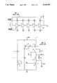
- FIG. 1A conventional ring oscillator circuit design is illustrated schematically in FIG. 1.
- the basic construction of such a ring oscillatorincludes an odd number of inverting delay stages, delay stages 1 1 -1 N , arranged in series in a ring configuration.
- a simple tracing of a DC signal through the ring oscillator of FIG. 1will show that a periodic signal is generated at the output, the output signal having a frequency of 1/2NT, where T is the delay of each inverting stage and N is the number of stages.
- the delay of each stagein turn is controlled by the control signal, illustrated as dashed lines 2 in FIG. 1, which signal is typically a control current.
- the control currentis in turn provided to each of the inverter gates 3 1 -3 N , as illustrated by the current source symbols for each stage.
- This control currentcontrols the switching speed of each inverter and hence the delay of each stage 1 1 -1 N .
- the overall arrangementis referred to as a voltage controlled oscillator (VCO).
- the ring oscillatorSince the ring oscillator is designed to provide a stable output frequency which varies as a function of the input control signal, it is desirable that the amount of delay be a linear function of the control signal. This linearity is approximately satisfied for conventional ring oscillator circuits at lower frequencies. As the frequency increases, however, transient effects due to the switching of the inverter gates 3 1 -3 N introduce significant nonlinearities, rendering the amount of delay a less predictable function of the control current.
- a conventional delay stage 1employs a CMOS inverter including p-channel and n-channel switching field effect transistors, 4 and 5, respectively. These switching transistors 4, 5 receive an input signal on the gates thereof provided from the preceding stage in the ring configuration. Switching transistors 4, 5 are coupled to V DD and ground, respectively, through transistors 6 and 7. Transistors 6, 7 are biased via diode connected p-channel and n-channel transistors 8 and 9, respectively. This configuration results in control bias voltages V P and V N applied to the gate of transistors 6 and 7, respectively, to control their respective resistances so as to mirror current I through these transistors.
- the delay of the stagewill essentially be the time it takes to charge the load capacitance C L by the current I.
- the switching speed of the transistors 4, 5will be relatively negligible relative to the charge time of the output load capacitance C L and therefore transient effects may be ignored and current I to the output treated as constant.
- the transient effectsbecome significant.
- the charging or discharging of the parasitic capacitances C PP and C PNcause significant fluctuations in the current flow.
- the time to charge C Land thus the overall delay time of the delay stage, is subject to fluctuations.
- the present inventionprovides a high frequency clock signal synthesizer circuit which provides one or more variable high frequency signals having predictable frequency characteristics even at very high frequencies.
- the present inventionemploys a single externally provided reference clock signal, which is used to generate one or more output signals, each having a variable frequency.
- the reference clock signalis provided to a phase comparator.
- the phase comparatorcompares the phase of the reference signal and the output signal of the circuit, which output has been down converted in frequency by a counter, and generates a phase lag or lead signal.
- the countermay be set to a variable count value N by an externally provided delay control signal and a delay control register.
- a charge pumpestablishes a control voltage from these lag and lead signals and provides the control voltage to a voltage controlled oscillator. The magnitude of this control voltage is determined by N, the divide count of the counter. By controlling the count value N, several discrete frequencies may thus be provided from a single reference clock.
- the voltage controlled oscillatorincludes a ring oscillator having a frequency characteristic which is a highly linear function of the control current, even for very high frequencies.
- the ring oscillator of the present inventionemploys an odd number of inverting delay stages, each delay stage including an input, an output, an inverter, and a controllable current source positioned between the inverter and the output.
- the controllable current sourcebuffers the output from parasitic capacitances of the switching transistors of the inverter
- a bias networkis employed to receive an input control current and mirror the control current in the current source in each of the delay stages of the ring oscillator.
- the bias networkincludes a load matching the loads of the switching transistors in the inverters. This additional load in the bias network allows the control current to be replicated exactly in each of the delay stages. This provides a reproducible control current directly at the output to thereby control the charging of the output capacitance, and hence the delay of each stage, in a manner which is a substantially linear function of the control signal.
- each delay stage of the ring oscillatoremploys a CMOS inverter having an input coupled to the gates of a p-channel and an n-channel switching FET.
- P-channel and n-channel current source FETsare provided between the switching FETs and the output.
- the gates of the current source transistorsare biased by a biasing network.
- the biasing networkreceives the control signal, for example, from a voltage to current converter in the case of a voltage controlled oscillator application, and biases the current source transistors to a desired current value.
- the biasing networkincludes a p-channel biasing circuit and an n-channel biasing circuit.
- the p-channel biasing circuitincludes a p-channel load transistor and a diode connected p-channel transistor to bias the p-channel branch of the delay stage.
- the n-channel biasing circuitsimilarly includes an n-channel load transistor and a diode coupled n-channel transistor for the n-channel branch of the delay stage.
- This biasing networkthus matches the loads in the delay stage and results in the control current being mirrored in the p-channel and n-channel branches of the delay stage, respectively. Due to the current source transistors coupled directly to the output, the effects of the parasitic capacitances of the switching transistors forming the inverter are buffered from the output during transitions. This prevents the parasitic capacitances from introducing nonlinearities into the current at the output and thus rendering the delay a nonlinear function of the control current.
- FIG. 1is an electrical schematic drawing of a prior art ring oscillator circuit.
- FIG. 2is an electrical schematic drawing of a prior art delay stage such as employed in the ring oscillator circuit of FIG. 1.
- FIG. 3is an electrical schematic drawing of a high frequency clock signal synthesizer circuit in accordance with the present invention.
- FIG. 4is an electrical schematic drawing of a ring oscillator circuit in accordance with the present invention.
- FIG. 5is an electrical schematic drawing of a delay circuit in accordance with the present invention.
- FIG. 6ais a graphical representation of the response of the prior art delay circuit of FIG. 2 to a step voltage input.
- FIG. 6bis a graphical representation of the response of the delay circuit of the present invention to a step voltage input.
- the frequency synthesizer circuitemploys two matching variable frequency synthesizer circuits 10a and 10b for providing output frequencies FREQ1 and FREQ2, respectively.
- This configurationallows two adjustable high frequency signals to be generated in a compact chip layout.
- one preferred applicationis in a video graphics board where a pixel clock and a video memory clock signal may be provided as FREQ1 and FREQ2, respectively, in a compact circuit readily implemented in a single integrated circuit chip.
- a single high frequency signal synthesizer circuit 10amay be employed.
- additional matching high frequency signal synthesizer circuitsmay be provided where the application requires three or more separate high frequency signals to be generated.
- circuit 10areceives an externally provided signal REF, which may be provided by an external clock generation chip or other source of high frequency periodic signals.
- the circuit 10a of FIG. 3employs a phase comparator 11a, which may be of conventional design, to phase compare the input reference signal to the output signal FREQ1, which output is circulated back from the output of the circuit through counter 12a.
- Counter 12aprovides an adjustable down conversion in frequency by a count divide factor 1/N to signal FREQ1.
- the divide count factor 1/Nis variable and is set by frequency register 13a which receives an externally provided frequency setting signal.
- the conversion factor Nmay be set to one of 256 different values by the frequency setting signal and frequency register 13a. These various settings in turn allow the frequency of the output signal FREQ1 to be varied in discrete frequency steps. Providing a separate register 13b in turn allows the second output signal FREQ2 to have a different frequency.
- two separate clock signals FREQ1 and FREQ2may be provided, each adjustable over a wide frequency range, while only a single off chip reference clock signal REF is required. This could, for example, be employed to generate a pixel clock signal and memory clock signal in a video graphics board where different applications of the board require different clock frequencies.
- the phase comparator 11adetermines whether the reference frequency lags or leads the output frequency FREQ1, in the former case providing an up signal and in the latter case providing a down signal, to charge pump 14a.
- Charge pump 14ain conjunction with filter 15a, stores repeated up or down signals provided from the phase comparator 11a to build up a control voltage V C at node 16a. The number of such signals and hence the magnitude of the control voltage will be determined by the count number N of counter 12a.
- This control voltageis in turn provided to a voltage controlled oscillator including voltage to current converter 17a and ring oscillator 18a.
- Converter 17amay preferably employ a Wilson current source and a conventional voltage to current converter circuit.
- the voltage to current converter 17aprovides a control current I C , corresponding to the control voltage V C , to ring oscillator 18a.
- Ring oscillator 18ain turn provides the high frequency output signal FREQ1 which has a frequency which is a linear function of the control current I C .
- the structure and operation of ring oscillator 18ais described in detail below with reference to FIGS. 4 and 5.
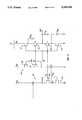
- a preferred embodiment of the ring oscillator circuit 18a of the present inventionis illustrated in an electrical schematic form.
- the ring oscillator circuit 18aincludes three delay stages 19, 20, 21. It will be appreciated, however, that any odd number of delay stages may be employed with three delay stages being chosen merely for ease of illustration.
- the specific layout shown in FIG. 4is illustrative only and various other configurations may be employed without departing from the present invention.
- the preferred embodiment illustrated in FIG. 4is shown implemented in a complementary metal oxide semiconductor (CMOS) implementation, other implementations such as NMOS or PMOS are also possible.
- CMOScomplementary metal oxide semiconductor
- delay stages 19, 20, 21each include a CMOS inverter coupled between a first reference voltage V DD and a second reference potential; for example, V DD may be +5 volts for typical CMOS applications and the second reference potential may be ground.
- delay stage 19includes a CMOS inverter formed by p-channel transistor 22 and n-channel transistor 23, coupled to V DD and ground, respectively. This inverter formed by the transistors 22 and 23 receives an input signal provided at input node 24 and provides an inverted signal at output node 25. The output at node 25 in turn is provided to the input node 26 of delay stage 20.
- Delay stage 20similarly employs a CMOS inverter formed by p-channel transistor 28 and n-channel transistor 30 to invert the signal at input node 26 and provide the inverted signal at output node 32.
- third delay stage 21includes input node 34, an inverter formed by p-channel transistor 36 and n-channel transistor 38, and output node 40.
- the output signal at output node 40is in turn coupled back to input node 24 of the first delay stage 19 to form the ring configuration. Additionally, the output at node 40 is provided to ring oscillator output 42 to provide the desired oscillating output signal.
- the configuration of an odd number of inverting delay stages 19, 20, 21 in a ring configurationresults in an oscillating output signal having a frequency (f) of 1/2NT, where N is the number of stages and T is the delay of each stage.
- ffrequency of 1/2NT
- each delay stagefurther includes a first and second current source configured between the p and n-channel transistors making up the CMOS inverter and the output node of each stage. More specifically, first inverting delay stage 19 includes a first current source 44 and second current source 46 coupled between inverting transistors 22, 23 and output node 25. Similarly, second delay stage 20 includes a first current source 48 and second current source 50 coupled between inverting transistors 28, 30 and output node 32, and third delay stage 21 includes first and second current sources 52, 54 coupled between transistors 36, 38 and output node 40.
- Each of the first current sources 44, 48 and 52are driven by a first biasing circuit 56 which mirrors control current I at each of the delay stages.
- the first biasing circuit 56includes load 58 to match the load in the p-channel legs of delay stages 19, 20 and 21.
- second current sources 46, 50 and 54are driven by a second bias circuit 60 having load 62 which matches that in the n-channel legs of each of the delay stages 19, 20 and 21.
- the first and second bias circuits 56, 60thus allow control current I, established therein by externally provided control signals, to be mirrored in each of the first and second current sources 44, 46, 48, 50, 52 and 54.
- the ring oscillator of the present inventionprovides a stable current source between each of the switching transistors 22, 23, 28, 30, 36, 38 of the inverters of each delay stage and the respective delay stage output node.
- These stable current sources 44-54provide a buffer between the output node and the transient effects associated with the switching action of the p-channel and n-channel transistors making up the inverters of each delay stage. Since the delay (T) of each stage is proportional to the current flowing through the output node thereof, it will be appreciated that the provision of a stable current I at the output node serves to establish a well defined delay. Therefore, the ring oscillator of FIG. 4 provides an oscillating signal at output 42 having a frequency which is a well defined function of the control signal.
- FIG. 5a specific implementation of the biasing circuit in conjunction with a single delay stage is illustrated.
- the delay stage illustrated in FIG. 5may be taken to correspond to delay stage 19 in FIG. 4 and like numerals are used accordingly.
- the parasitic capacitances of various circuit elementsare illustrated schematically therein.
- the first and second current sources, 44, 46, respectivelymay take the form of p-channel and n-channel transistors with their gates tied to the first and second bias circuits, 56, 60, respectively.
- First bias circuit 56includes a p-channel transistor 62 with its gate coupled to ground so as to mirror the load provided by p-channel switching transistor 22 when it is in an on state.
- First bias circuit 56further includes a second p-channel transistor 64 in a diode coupled configuration.
- P-channel transistor 64has its gate tied to the gate of p-channel transistor 44 thereby also ensuring that transistor 64 mirrors the load of current source 44.
- second bias circuit 60includes an n-channel transistor 66 with its gate coupled to V DD , transistor 66 matching n-channel switching transistor 23 in load characteristics when it is in an on state. Second bias circuit 60 also includes diode connected n-channel transistor 68 with its gate tied to n-channel transistor 46 to thereby mirror load characteristics of transistor 46. In the same way, the current I established in the second bias circuit 60 is mirrored in transistor 46 as indicated.
- the parasitic capacitance C PP of the p-channel switching transistor 22, the parasitic capacitance C PN of the n-channel switching transistor 23 and the output load capacitance C Lare buffered from the output load capacitance C L by the current source transistors 44, 46. Therefore, no charge sharing occurs between parasitic capacitances C PP , C PN and output load capacitance C L , avoiding transient effects in the charging of the output capacitance C L by the current I. Also, the positioning of the current source transistors adjacent the output node provides a high output impedance during transitions at the input, which limits the current flow into C L to a value equal to or less than I. It will thus be appreciated that the reconfiguration of the switching inverter transistors 22, 23 outside current source transistors 44, 46 significantly increases the predictability and linearity of the delay circuit 19 in response to high frequency transitions.
- the reduction in parasitic and other transient effects by the illustrated configuration of FIG. 5may be appreciated qualitatively by considering the operation during a transition at the input node, e.g., from a 1 to 0 logic state (V DD to ground).
- V DDlogic state
- the output capacitance C Lhas been discharged to ground through the conductive n-channel transistors 46 and 23.
- the p-channel switching transistor 22is off and the voltage on the p-channel parasitic capacitance is exactly equal to one threshold above the bias voltage V P applied to the gate of p-channel transistor 44.
- the p-channel switching transistor 22begins to turn on and the parasitic capacitance thereof moves toward the power supply V DD until it reaches the same voltage as point A in the first bias circuit.
- the current source to the load capacitance C Lis equal to I, as desired, and C L is charged with a time constant determined linearly by I.
- the p-channel current source transistor 44since the p-channel current source transistor 44 always starts in the saturation region, the output impedance thereof is high at the beginning of the transition. Therefore, the charge on the p-channel parasitic capacitance C PP never gets shared with the charge on the output load capacitance C L , due to the buffering of the saturated transistor 44.
- the rate of charging of the output load capacitance C Lis always a function of the current in the current source transistor 44 and does not jump during a fast input transition as in conventional delay stages. Furthermore, since the parasitic capacitance is a very process dependent variable, and the capacitance of C L is user defined, the buffering provided by the saturated current source transistors 44 and 46 which serves to isolate the capacitance of C L from the capacitance of C PP and C PN allows a more controllable delay in the face of process variations.
- FIG. 6bThe foregoing qualitative advantages of the delay stage of the present invention are illustrated graphically in FIG. 6b and may be compared to a conventional delay stage illustrated in FIG. 6a.
- the graphs of FIGS. 6a and 6billustrate the voltage versus time characteristics of the output node of a delay stage in response to a step transition at the input thereof. That is, at approximately 1 nanosecond (ns), the input begins a transition from 0 to 1 (ground to V DD ) then at approximately 9 ns, the input begins a sharp transition from 1 to 0 (V DD to ground).
- the graphical representations of FIG. 6a and 6bwere generated by a computer simulation of the basic circuit configurations of FIGS. 2 and 5, respectively.
- the transition from 0 to +5 voltsresults in a very smooth curve having a relatively constant slope dV/dt through substantially the entire transition time.
- the transitionis smooth and results in a substantially constant slope dV/dt.
- the present inventionprovides a much more constant current throughout the transition time as compared to a conventional delay stage. Accordingly, the delay time provided by the delay stage can be a relatively predictable function of the control signal and will be stable at even relatively high oscillation frequencies.
Landscapes
- Pulse Circuits (AREA)
Abstract
Description
Claims (7)
Priority Applications (1)
| Application Number | Priority Date | Filing Date | Title |
|---|---|---|---|
| US07/666,224US5136260A (en) | 1991-03-08 | 1991-03-08 | PLL clock synthesizer using current controlled ring oscillator |
Applications Claiming Priority (1)
| Application Number | Priority Date | Filing Date | Title |
|---|---|---|---|
| US07/666,224US5136260A (en) | 1991-03-08 | 1991-03-08 | PLL clock synthesizer using current controlled ring oscillator |
Publications (1)
| Publication Number | Publication Date |
|---|---|
| US5136260Atrue US5136260A (en) | 1992-08-04 |
Family
ID=24673325
Family Applications (1)
| Application Number | Title | Priority Date | Filing Date |
|---|---|---|---|
| US07/666,224Expired - LifetimeUS5136260A (en) | 1991-03-08 | 1991-03-08 | PLL clock synthesizer using current controlled ring oscillator |
Country Status (1)
| Country | Link |
|---|---|
| US (1) | US5136260A (en) |
Cited By (59)
| Publication number | Priority date | Publication date | Assignee | Title |
|---|---|---|---|---|
| US5281927A (en)* | 1993-05-20 | 1994-01-25 | Codex Corp. | Circuit and method of controlling a VCO with capacitive loads |
| US5289060A (en)* | 1992-09-16 | 1994-02-22 | Texas Instruments Incorporated | Programmable glitch filter |
| US5300823A (en)* | 1991-07-17 | 1994-04-05 | Sharp Kabushiki Kaisha | Internal voltage dropping circuit for semiconductor device |
| US5302920A (en)* | 1992-10-13 | 1994-04-12 | Ncr Corporation | Controllable multi-phase ring oscillators with variable current sources and capacitances |
| US5331295A (en)* | 1993-02-03 | 1994-07-19 | National Semiconductor Corporation | Voltage controlled oscillator with efficient process compensation |
| US5334951A (en)* | 1993-02-18 | 1994-08-02 | Northern Telecom Limited | Phase lock loops and methods for their operation |
| WO1994017592A1 (en)* | 1993-01-19 | 1994-08-04 | Credence Systems Corporation | Retriggered oscillator for jitter-free phase locked loop frequency synthesis |
| US5349311A (en)* | 1992-11-23 | 1994-09-20 | National Semiconductor Corporation | Current starved inverter voltage controlled oscillator |
| US5373257A (en)* | 1992-10-28 | 1994-12-13 | Fujitsu Limited | Phase synchronization circuit having a loop filter including two voltage/current converters |
| US5382921A (en)* | 1992-11-23 | 1995-01-17 | National Semiconductor Corporation | Automatic selection of an operating frequency in a low-gain broadband phase lock loop system |
| US5406228A (en)* | 1994-07-12 | 1995-04-11 | General Instrument | Ring oscillator with frequency control loop |
| US5471176A (en)* | 1994-06-07 | 1995-11-28 | Quantum Corporation | Glitchless frequency-adjustable ring oscillator |
| US5477198A (en)* | 1994-06-23 | 1995-12-19 | At&T Global Information Solutions Company | Extendible-range voltage controlled oscillator |
| US5485126A (en)* | 1994-01-25 | 1996-01-16 | International Business Machines Corporation | Ring oscillator circuit having output with fifty percent duty cycle |
| US5495512A (en)* | 1994-09-12 | 1996-02-27 | Analog Devices, Inc. | Hybrid phase locked loop |
| US5552733A (en)* | 1993-01-19 | 1996-09-03 | Credence Systems Corporation | Precise and agile timing signal generator based on a retriggered oscillator |
| US5559473A (en)* | 1994-06-23 | 1996-09-24 | At&T Global Information Solutions Company | Multi-range voltage controlled oscillator |
| US5559477A (en)* | 1994-02-10 | 1996-09-24 | International Microcircuits, Inc. | Pulse generator having controlled delay to control duty cycle |
| US5576666A (en)* | 1993-11-12 | 1996-11-19 | Nippondenso Technical Center Usa, Inc. | Fractional-N frequency synthesizer with temperature compensation |
| US5617454A (en)* | 1994-07-15 | 1997-04-01 | U.S. Philips Corporation | Transmission system |
| US5657359A (en)* | 1994-11-04 | 1997-08-12 | Fujitsu, Limited | Phase synchronizer and data reproducing apparatus |
| DE19703986A1 (en)* | 1996-05-31 | 1997-12-04 | Mitsubishi Electric Corp | Signal shaper for input signal wave form reshaping |
| US5705947A (en)* | 1994-06-06 | 1998-01-06 | Deog-Kyoon Jeog | Clock generator |
| US5748050A (en)* | 1996-03-29 | 1998-05-05 | Symbios Logic Inc. | Linearization method and apparatus for voltage controlled oscillator |
| US5770975A (en)* | 1996-01-24 | 1998-06-23 | Nec Corporation | Phase-locked loop circuit having a high-speed forcible pulling-in function |
| US5781055A (en)* | 1996-05-31 | 1998-07-14 | Sun Microsystems, Inc. | Apparatus and method for instantaneous stretching of clock signals in a delay-locked loop multi-phase clock generator |
| US5861766A (en)* | 1997-04-17 | 1999-01-19 | Western Digital Corporation | Multimode frequency synthesizer having high loop gain in frequency seek mode |
| US5898336A (en)* | 1996-08-21 | 1999-04-27 | Nec Corporation | Charging pump circuit and a phase-locked loop circuit using the same |
| US6157266A (en)* | 1998-02-12 | 2000-12-05 | Hewlett-Packard Company | Delay elements arranged for a signal controlled oscillator |
| US6188285B1 (en)* | 1998-10-23 | 2001-02-13 | Mitsubishi Denki Kabushiki Kaisha | Phase-locked loop circuit and voltage-controlled oscillator capable of producing oscillations in a plurality of frequency ranges |
| US6194929B1 (en)* | 1997-06-25 | 2001-02-27 | Sun Microsystems, Inc. | Delay locking using multiple control signals |
| US6211727B1 (en)* | 1998-02-26 | 2001-04-03 | Stmicroelectronics, Inc. | Circuit and method for intelligently regulating a supply voltage |
| EP1120912A1 (en)* | 1993-02-05 | 2001-08-01 | Sun Microsystems, Inc. | Method and apparatus for timing control |
| US6586986B2 (en)* | 2000-12-27 | 2003-07-01 | Hynix Semiconductor Inc. | Circuit for generating internal power voltage in a semiconductor device |
| US20030179318A1 (en)* | 2002-03-22 | 2003-09-25 | Mohammad Alkhalili | Self-adjusting pixel clock and method therefor |
| US20040012449A1 (en)* | 2002-07-16 | 2004-01-22 | Illegems Paul F. | Ring oscillator with frequency stabilization |
| US7095348B1 (en) | 2000-05-23 | 2006-08-22 | Marvell International Ltd. | Communication driver |
| US7113121B1 (en) | 2000-05-23 | 2006-09-26 | Marvell International Ltd. | Communication driver |
| EP1359592A3 (en)* | 1995-10-31 | 2006-12-20 | STMicroelectronics S.r.l. | Clock generator for electrically programmable nonvolatile memory cells |
| US20070057735A1 (en)* | 2005-09-12 | 2007-03-15 | P.A. Semi, Inc. | Voltage-controlled oscillator for low-voltage, wide frequency range operation |
| US7194037B1 (en) | 2000-05-23 | 2007-03-20 | Marvell International Ltd. | Active replica transformer hybrid |
| US7312662B1 (en) | 2005-08-09 | 2007-12-25 | Marvell International Ltd. | Cascode gain boosting system and method for a transmitter |
| US7312739B1 (en) | 2000-05-23 | 2007-12-25 | Marvell International Ltd. | Communication driver |
| US7327995B1 (en) | 2000-07-31 | 2008-02-05 | Marvell International Ltd. | Active resistance summer for a transformer hybrid |
| EP1916769A1 (en)* | 2006-10-27 | 2008-04-30 | Interuniversitair Microelektronica Centrum | Device and method for generating a signal with predefined transient at start-up |
| EP1916768A1 (en)* | 2006-10-27 | 2008-04-30 | Interuniversitair Micro-Elektronica Centrum Vzw | Device and method for generating a signal with predefined transient at start-up |
| US20080111639A1 (en)* | 2006-10-27 | 2008-05-15 | Interuniversitair Microelektronica Centrum (Imec) | Device and method for generating a signal with predefined transcient at start-up |
| US7433665B1 (en) | 2000-07-31 | 2008-10-07 | Marvell International Ltd. | Apparatus and method for converting single-ended signals to a differential signal, and transceiver employing same |
| US7577892B1 (en) | 2005-08-25 | 2009-08-18 | Marvell International Ltd | High speed iterative decoder |
| US7606547B1 (en) | 2000-07-31 | 2009-10-20 | Marvell International Ltd. | Active resistance summer for a transformer hybrid |
| USRE40971E1 (en) | 2000-12-18 | 2009-11-17 | Marvell International Ltd. | Direct drive programmable high speed power digital-to-analog converter |
| USRE41831E1 (en) | 2000-05-23 | 2010-10-19 | Marvell International Ltd. | Class B driver |
| USRE42250E1 (en)* | 1994-12-29 | 2011-03-29 | Stmicroelectronics, Inc. | Delay circuit and method |
| US20110080381A1 (en)* | 2009-10-06 | 2011-04-07 | Mstar Semiconductor, Inc. | Portable Control Apparatus and Method Thereof |
| US8111107B2 (en)* | 2010-07-07 | 2012-02-07 | Taiwan Semiconductor Manufacturing Company, Ltd. | Charge pump control scheme |
| TWI594576B (en)* | 2013-02-25 | 2017-08-01 | 三星電子股份有限公司 | Phase locked loop for preventing harmonic lock, method of operating the same, and devices including the same |
| TWI697210B (en)* | 2019-05-10 | 2020-06-21 | 國立中山大學 | Phase-locked loop with automatic band selector and multi-band voltage control oscillator thereof |
| CN115184762A (en)* | 2022-07-12 | 2022-10-14 | 长鑫存储技术有限公司 | Test circuit, test method and device using test circuit |
| US11894850B1 (en)* | 2022-09-16 | 2024-02-06 | Changxin Memory Technologies, Inc. | Delay circuits and semiconductor devices |
Citations (2)
| Publication number | Priority date | Publication date | Assignee | Title |
|---|---|---|---|---|
| US4988960A (en)* | 1988-12-21 | 1991-01-29 | Yamaha Corporation | FM demodulation device and FM modulation device employing a CMOS signal delay device |
| US5036216A (en)* | 1990-03-08 | 1991-07-30 | Integrated Circuit Systems, Inc. | Video dot clock generator |
- 1991
- 1991-03-08USUS07/666,224patent/US5136260A/ennot_activeExpired - Lifetime
Patent Citations (2)
| Publication number | Priority date | Publication date | Assignee | Title |
|---|---|---|---|---|
| US4988960A (en)* | 1988-12-21 | 1991-01-29 | Yamaha Corporation | FM demodulation device and FM modulation device employing a CMOS signal delay device |
| US5036216A (en)* | 1990-03-08 | 1991-07-30 | Integrated Circuit Systems, Inc. | Video dot clock generator |
Non-Patent Citations (2)
| Title |
|---|
| "Design of PLL-Based Clock Generation Circuits", D. K. Jeong, et al., IEEE Journal of Solid State Circuits, vol. SC-22, No. 2, Apr. 1987, pp. 255-261. |
| Design of PLL Based Clock Generation Circuits , D. K. Jeong, et al., IEEE Journal of Solid State Circuits, vol. SC 22, No. 2, Apr. 1987, pp. 255 261.* |
Cited By (82)
| Publication number | Priority date | Publication date | Assignee | Title |
|---|---|---|---|---|
| US5300823A (en)* | 1991-07-17 | 1994-04-05 | Sharp Kabushiki Kaisha | Internal voltage dropping circuit for semiconductor device |
| US5289060A (en)* | 1992-09-16 | 1994-02-22 | Texas Instruments Incorporated | Programmable glitch filter |
| US5302920A (en)* | 1992-10-13 | 1994-04-12 | Ncr Corporation | Controllable multi-phase ring oscillators with variable current sources and capacitances |
| US5373257A (en)* | 1992-10-28 | 1994-12-13 | Fujitsu Limited | Phase synchronization circuit having a loop filter including two voltage/current converters |
| US5349311A (en)* | 1992-11-23 | 1994-09-20 | National Semiconductor Corporation | Current starved inverter voltage controlled oscillator |
| US5382921A (en)* | 1992-11-23 | 1995-01-17 | National Semiconductor Corporation | Automatic selection of an operating frequency in a low-gain broadband phase lock loop system |
| WO1994017592A1 (en)* | 1993-01-19 | 1994-08-04 | Credence Systems Corporation | Retriggered oscillator for jitter-free phase locked loop frequency synthesis |
| US5345186A (en)* | 1993-01-19 | 1994-09-06 | Credence Systems Corporation | Retriggered oscillator for jitter-free phase locked loop frequency synthesis |
| US5552733A (en)* | 1993-01-19 | 1996-09-03 | Credence Systems Corporation | Precise and agile timing signal generator based on a retriggered oscillator |
| US5331295A (en)* | 1993-02-03 | 1994-07-19 | National Semiconductor Corporation | Voltage controlled oscillator with efficient process compensation |
| EP1120912A1 (en)* | 1993-02-05 | 2001-08-01 | Sun Microsystems, Inc. | Method and apparatus for timing control |
| US5334951A (en)* | 1993-02-18 | 1994-08-02 | Northern Telecom Limited | Phase lock loops and methods for their operation |
| US5281927A (en)* | 1993-05-20 | 1994-01-25 | Codex Corp. | Circuit and method of controlling a VCO with capacitive loads |
| US5576666A (en)* | 1993-11-12 | 1996-11-19 | Nippondenso Technical Center Usa, Inc. | Fractional-N frequency synthesizer with temperature compensation |
| US5485126A (en)* | 1994-01-25 | 1996-01-16 | International Business Machines Corporation | Ring oscillator circuit having output with fifty percent duty cycle |
| US5559477A (en)* | 1994-02-10 | 1996-09-24 | International Microcircuits, Inc. | Pulse generator having controlled delay to control duty cycle |
| US5705947A (en)* | 1994-06-06 | 1998-01-06 | Deog-Kyoon Jeog | Clock generator |
| US5471176A (en)* | 1994-06-07 | 1995-11-28 | Quantum Corporation | Glitchless frequency-adjustable ring oscillator |
| US5559473A (en)* | 1994-06-23 | 1996-09-24 | At&T Global Information Solutions Company | Multi-range voltage controlled oscillator |
| US5477198A (en)* | 1994-06-23 | 1995-12-19 | At&T Global Information Solutions Company | Extendible-range voltage controlled oscillator |
| EP0692879B1 (en)* | 1994-07-12 | 2003-12-10 | General Instrument Corporation | Ring oscillator with frequency control loop |
| US5406228A (en)* | 1994-07-12 | 1995-04-11 | General Instrument | Ring oscillator with frequency control loop |
| US5617454A (en)* | 1994-07-15 | 1997-04-01 | U.S. Philips Corporation | Transmission system |
| US5495512A (en)* | 1994-09-12 | 1996-02-27 | Analog Devices, Inc. | Hybrid phase locked loop |
| US5657359A (en)* | 1994-11-04 | 1997-08-12 | Fujitsu, Limited | Phase synchronizer and data reproducing apparatus |
| US5982836A (en)* | 1994-11-04 | 1999-11-09 | Fujitsu Limited | Phase synchronizer and data reproducing apparatus |
| USRE42250E1 (en)* | 1994-12-29 | 2011-03-29 | Stmicroelectronics, Inc. | Delay circuit and method |
| EP1359592A3 (en)* | 1995-10-31 | 2006-12-20 | STMicroelectronics S.r.l. | Clock generator for electrically programmable nonvolatile memory cells |
| US5770975A (en)* | 1996-01-24 | 1998-06-23 | Nec Corporation | Phase-locked loop circuit having a high-speed forcible pulling-in function |
| US6285263B1 (en) | 1996-03-29 | 2001-09-04 | Lsi Logic Corporation | Linearization method and apparatus for voltage controlled oscillator |
| US5748050A (en)* | 1996-03-29 | 1998-05-05 | Symbios Logic Inc. | Linearization method and apparatus for voltage controlled oscillator |
| DE19703986C2 (en)* | 1996-05-31 | 1999-09-02 | Mitsubishi Electric Corp | Waveform shaping device and clock signal feed device |
| US5883534A (en)* | 1996-05-31 | 1999-03-16 | Mitsubishi Denki Kabushiki Kaisha | Waveform shaping device and clock supply apparatus |
| DE19703986A1 (en)* | 1996-05-31 | 1997-12-04 | Mitsubishi Electric Corp | Signal shaper for input signal wave form reshaping |
| US5781055A (en)* | 1996-05-31 | 1998-07-14 | Sun Microsystems, Inc. | Apparatus and method for instantaneous stretching of clock signals in a delay-locked loop multi-phase clock generator |
| US5898336A (en)* | 1996-08-21 | 1999-04-27 | Nec Corporation | Charging pump circuit and a phase-locked loop circuit using the same |
| US5861766A (en)* | 1997-04-17 | 1999-01-19 | Western Digital Corporation | Multimode frequency synthesizer having high loop gain in frequency seek mode |
| US6194929B1 (en)* | 1997-06-25 | 2001-02-27 | Sun Microsystems, Inc. | Delay locking using multiple control signals |
| US6157266A (en)* | 1998-02-12 | 2000-12-05 | Hewlett-Packard Company | Delay elements arranged for a signal controlled oscillator |
| US6211727B1 (en)* | 1998-02-26 | 2001-04-03 | Stmicroelectronics, Inc. | Circuit and method for intelligently regulating a supply voltage |
| US6188285B1 (en)* | 1998-10-23 | 2001-02-13 | Mitsubishi Denki Kabushiki Kaisha | Phase-locked loop circuit and voltage-controlled oscillator capable of producing oscillations in a plurality of frequency ranges |
| US8009073B2 (en) | 2000-05-23 | 2011-08-30 | Marvell International Ltd. | Method and apparatus for generating an analog signal having a pre-determined pattern |
| US7312739B1 (en) | 2000-05-23 | 2007-12-25 | Marvell International Ltd. | Communication driver |
| USRE41831E1 (en) | 2000-05-23 | 2010-10-19 | Marvell International Ltd. | Class B driver |
| US7095348B1 (en) | 2000-05-23 | 2006-08-22 | Marvell International Ltd. | Communication driver |
| US7113121B1 (en) | 2000-05-23 | 2006-09-26 | Marvell International Ltd. | Communication driver |
| US7804904B1 (en) | 2000-05-23 | 2010-09-28 | Marvell International Ltd. | Active replica transformer hybrid |
| US7729429B1 (en) | 2000-05-23 | 2010-06-01 | Marvell International Ltd. | Active replica transformer hybrid |
| US7194037B1 (en) | 2000-05-23 | 2007-03-20 | Marvell International Ltd. | Active replica transformer hybrid |
| US7649483B1 (en) | 2000-05-23 | 2010-01-19 | Marvell International Ltd. | Communication driver |
| US7606547B1 (en) | 2000-07-31 | 2009-10-20 | Marvell International Ltd. | Active resistance summer for a transformer hybrid |
| US8045946B2 (en) | 2000-07-31 | 2011-10-25 | Marvell International Ltd. | Active resistive summer for a transformer hybrid |
| US8880017B1 (en) | 2000-07-31 | 2014-11-04 | Marvell International Ltd. | Active resistive summer for a transformer hybrid |
| US8503961B1 (en) | 2000-07-31 | 2013-08-06 | Marvell International Ltd. | Active resistive summer for a transformer hybrid |
| US8050645B1 (en) | 2000-07-31 | 2011-11-01 | Marvell International Ltd. | Active resistive summer for a transformer hybrid |
| US7433665B1 (en) | 2000-07-31 | 2008-10-07 | Marvell International Ltd. | Apparatus and method for converting single-ended signals to a differential signal, and transceiver employing same |
| US7466971B1 (en) | 2000-07-31 | 2008-12-16 | Marvell International Ltd. | Active resistive summer for a transformer hybrid |
| US7536162B1 (en) | 2000-07-31 | 2009-05-19 | Marvell International Ltd. | Active resistive summer for a transformer hybrid |
| US7327995B1 (en) | 2000-07-31 | 2008-02-05 | Marvell International Ltd. | Active resistance summer for a transformer hybrid |
| US7761076B1 (en) | 2000-07-31 | 2010-07-20 | Marvell International Ltd. | Apparatus and method for converting single-ended signals to a differential signal, and transceiver employing same |
| USRE40971E1 (en) | 2000-12-18 | 2009-11-17 | Marvell International Ltd. | Direct drive programmable high speed power digital-to-analog converter |
| US6586986B2 (en)* | 2000-12-27 | 2003-07-01 | Hynix Semiconductor Inc. | Circuit for generating internal power voltage in a semiconductor device |
| US7136109B2 (en)* | 2002-03-22 | 2006-11-14 | Pelco | Self-adjusting pixel clock and method therefor |
| US20030179318A1 (en)* | 2002-03-22 | 2003-09-25 | Mohammad Alkhalili | Self-adjusting pixel clock and method therefor |
| US20040012449A1 (en)* | 2002-07-16 | 2004-01-22 | Illegems Paul F. | Ring oscillator with frequency stabilization |
| US7737788B1 (en) | 2005-08-09 | 2010-06-15 | Marvell International Ltd. | Cascode gain boosting system and method for a transmitter |
| US7312662B1 (en) | 2005-08-09 | 2007-12-25 | Marvell International Ltd. | Cascode gain boosting system and method for a transmitter |
| US7853855B1 (en) | 2005-08-25 | 2010-12-14 | Marvell International Ltd. | High speed iterative decoder |
| US7577892B1 (en) | 2005-08-25 | 2009-08-18 | Marvell International Ltd | High speed iterative decoder |
| US7268633B2 (en)* | 2005-09-12 | 2007-09-11 | P.A. Semi, Inc. | Voltage-controlled oscillator for low-voltage, wide frequency range operation |
| US20070057735A1 (en)* | 2005-09-12 | 2007-03-15 | P.A. Semi, Inc. | Voltage-controlled oscillator for low-voltage, wide frequency range operation |
| EP1916768A1 (en)* | 2006-10-27 | 2008-04-30 | Interuniversitair Micro-Elektronica Centrum Vzw | Device and method for generating a signal with predefined transient at start-up |
| US20080111639A1 (en)* | 2006-10-27 | 2008-05-15 | Interuniversitair Microelektronica Centrum (Imec) | Device and method for generating a signal with predefined transcient at start-up |
| US7719373B2 (en) | 2006-10-27 | 2010-05-18 | Imec | Device and method for generating a signal with predefined transcient at start-up |
| EP1916769A1 (en)* | 2006-10-27 | 2008-04-30 | Interuniversitair Microelektronica Centrum | Device and method for generating a signal with predefined transient at start-up |
| US20110080381A1 (en)* | 2009-10-06 | 2011-04-07 | Mstar Semiconductor, Inc. | Portable Control Apparatus and Method Thereof |
| US9093985B2 (en)* | 2009-10-06 | 2015-07-28 | Mstar Semiconductor, Inc. | Portable control apparatus and method thereof for calibrating an oscillating circuit |
| US8111107B2 (en)* | 2010-07-07 | 2012-02-07 | Taiwan Semiconductor Manufacturing Company, Ltd. | Charge pump control scheme |
| TWI594576B (en)* | 2013-02-25 | 2017-08-01 | 三星電子股份有限公司 | Phase locked loop for preventing harmonic lock, method of operating the same, and devices including the same |
| TWI697210B (en)* | 2019-05-10 | 2020-06-21 | 國立中山大學 | Phase-locked loop with automatic band selector and multi-band voltage control oscillator thereof |
| CN115184762A (en)* | 2022-07-12 | 2022-10-14 | 长鑫存储技术有限公司 | Test circuit, test method and device using test circuit |
| US11894850B1 (en)* | 2022-09-16 | 2024-02-06 | Changxin Memory Technologies, Inc. | Delay circuits and semiconductor devices |
Similar Documents
| Publication | Publication Date | Title |
|---|---|---|
| US5136260A (en) | PLL clock synthesizer using current controlled ring oscillator | |
| KR920004335B1 (en) | Voltage controlled oscillation circuit | |
| US5552748A (en) | Digitally-tuned oscillator including a self-calibrating RC oscillator circuit | |
| US5594388A (en) | Self-calibrating RC oscillator | |
| US5426384A (en) | Voltage controlled oscillator (VCO) with symmetrical output and logic gate for use in same | |
| US8212599B2 (en) | Temperature-stable oscillator circuit having frequency-to-current feedback | |
| US4641048A (en) | Digital integrated circuit propagation delay time controller | |
| Flynn et al. | A 1.2-mu m CMOS current-controlled oscillator | |
| EP0598260B1 (en) | High frequency voltage controlled oscillator | |
| EP0735677B1 (en) | Oscillator circuit having oscillation frequency independent from the supply voltage value | |
| US5485126A (en) | Ring oscillator circuit having output with fifty percent duty cycle | |
| US5663675A (en) | Multiple stage tracking filter using a self-calibrating RC oscillator circuit | |
| KR910008522B1 (en) | Voltage controlled oscillation circuit | |
| US7196561B2 (en) | Programmable reset signal that is independent of supply voltage ramp rate | |
| US5059838A (en) | Signal delay circuit using charge pump circuit | |
| US5463353A (en) | Resistorless VCO including current source and sink controlling a current controlled oscillator | |
| US6271730B1 (en) | Voltage-controlled oscillator including current control element | |
| JPH0879072A (en) | Ring oscillator with frequency control loop | |
| US5481228A (en) | Method and apparatus for controlling oscillator duty cycle | |
| US5585765A (en) | Low power RC oscillator using a low voltage bias circuit | |
| US5365204A (en) | CMOS voltage controlled ring oscillator | |
| KR100293769B1 (en) | Charge pumping circuit and PLL frequency synthesizer | |
| US5638029A (en) | Circuit for externally overdriving an internal clock | |
| US6211744B1 (en) | Ring oscillator having an externally adjustable variable frequency | |
| US4383224A (en) | NMOS Crystal oscillator |
Legal Events
| Date | Code | Title | Description |
|---|---|---|---|
| AS | Assignment | Owner name:BANK OF AMERICA NATIONAL TRUST AND SAVINGS ASSOCIA Free format text:SECURITY INTEREST;ASSIGNOR:WESTERN DIGITAL CORPORATION, A CORP. OF DE;REEL/FRAME:005926/0103 Effective date:19911031 | |
| STCF | Information on status: patent grant | Free format text:PATENTED CASE | |
| FPAY | Fee payment | Year of fee payment:4 | |
| AS | Assignment | Owner name:BANKBOSTON, N.A., AS AGENT, MASSACHUSETTS Free format text:PATENT COLLATERAL ASSIGNMENT AND SECURITY AGREEMENT DATED AS OF NOVEMBER 4, 1998;ASSIGNOR:WESTERN DIGITAL CORPORATION, A DELAWARE CORPORATION;REEL/FRAME:009596/0487 Effective date:19981104 | |
| FPAY | Fee payment | Year of fee payment:8 | |
| AS | Assignment | Owner name:WESTERN DIGITAL CORPORATION, CALIFORNIA Free format text:RELEASE BY SECURED PARTY;ASSIGNOR:FLEET NATIONAL BANK (F/K/A BANKBOSTON, N.A.);REEL/FRAME:011089/0459 Effective date:20000330 | |
| AS | Assignment | Owner name:GENERAL ELECTRIC CAPITAL CORPORATION, CALIFORNIA Free format text:SECURITY AGREEMENT;ASSIGNOR:WESTERN DIGITAL CORPORATION;REEL/FRAME:011170/0948 Effective date:20000920 | |
| AS | Assignment | Owner name:WESTERN DIGITAL TECHNOLOGIES, INC., CALIFORNIA Free format text:AMENDED AND RESTATED CERTIFICATE OF INCORPORATION OF WESTERN DIGITAL CORP.;ASSIGNOR:WESTERN DIGITAL CORPORATION;REEL/FRAME:011967/0481 Effective date:20010406 | |
| FPAY | Fee payment | Year of fee payment:12 | |
| AS | Assignment | Owner name:WESTERN DIGITAL TECHNOLOGIES, INC., CALIFORNIA Free format text:RELEASE BY SECURED PARTY;ASSIGNOR:GENERAL ELECTRIC CAPITAL CORPORATION, AS AGENT;REEL/FRAME:021502/0451 Effective date:20070809 |