US5134399A - Subranging analog-to-digital converter with dither - Google Patents
Subranging analog-to-digital converter with ditherDownload PDFInfo
- Publication number
- US5134399A US5134399AUS07/593,441US59344190AUS5134399AUS 5134399 AUS5134399 AUS 5134399AUS 59344190 AUS59344190 AUS 59344190AUS 5134399 AUS5134399 AUS 5134399A
- Authority
- US
- United States
- Prior art keywords
- bit
- analog
- word
- digital
- signal
- Prior art date
- Legal status (The legal status is an assumption and is not a legal conclusion. Google has not performed a legal analysis and makes no representation as to the accuracy of the status listed.)
- Expired - Lifetime
Links
- 238000006243chemical reactionMethods0.000claimsabstractdescription40
- 238000000034methodMethods0.000claimsdescription11
- 239000002131composite materialSubstances0.000claimsdescription9
- 230000000694effectsEffects0.000description5
- 238000010586diagramMethods0.000description2
- 230000003321amplificationEffects0.000description1
- 230000003247decreasing effectEffects0.000description1
- 230000002939deleterious effectEffects0.000description1
- 238000003199nucleic acid amplification methodMethods0.000description1
- 230000035945sensitivityEffects0.000description1
- 230000007704transitionEffects0.000description1
Images

Classifications
- H—ELECTRICITY
- H03—ELECTRONIC CIRCUITRY
- H03M—CODING; DECODING; CODE CONVERSION IN GENERAL
- H03M1/00—Analogue/digital conversion; Digital/analogue conversion
- H03M1/12—Analogue/digital converters
- H03M1/20—Increasing resolution using an n bit system to obtain n + m bits
- H03M1/201—Increasing resolution using an n bit system to obtain n + m bits by dithering
- H—ELECTRICITY
- H03—ELECTRONIC CIRCUITRY
- H03M—CODING; DECODING; CODE CONVERSION IN GENERAL
- H03M1/00—Analogue/digital conversion; Digital/analogue conversion
- H03M1/12—Analogue/digital converters
- H03M1/14—Conversion in steps with each step involving the same or a different conversion means and delivering more than one bit
- H03M1/144—Conversion in steps with each step involving the same or a different conversion means and delivering more than one bit the steps being performed sequentially in a single stage, i.e. recirculation type
Definitions
- the present inventionrelates to subranging analog-to-digital converters employing dither to improve resolution accuracy, and more particularly relates to such converters wherein the dither is resolved to bits that are nominally insignificant with respect to the converter's internal ADC.
- Subranging analog-to-digital convertersare well known in the art, as shown by U.S. Pat. Nos. 3,597,761, 3,956,746, 4,550,309 and 4,733,217.
- U.S. Pat. No. 4,550,309shows a residue converter in which resolution is enhanced by introducing a random dither signal into the process.
- the apparatus 10 disclosed in U.S. Pat. No. 4,500,309includes a sample and hold circuit 12, first pass and second pass scaling circuits 14, 16, an 8-bit analog-to-digital (ADC) converter 18, a digital-to-analog converter (DAC) 20, an analog difference circuit 22, a 13-bit accumulator 24, and a 13-bit latch 26.
- ADCanalog-to-digital
- DACdigital-to-analog converter
- To these foregoing elementsare added a digital noise source 28, a second 13-bit accumulator 30, and a second 13-bit latch 32.
- the converter 10operates by first scaling an analog input signal by a factor of K in scaling circuit 14.
- the scaled analog input signalis then converted into a first pass 8-bit digital word approximately corresponding thereto by the ADC 18.
- the first pass output from ADC 18is loaded into the 8 most significant bits of the 13-bit second accumulator 30.
- a 6-bit digital noise word from noise source 28is loaded into the least significant bits of this accumulator, forming a one-bit overlap with the ADC output word.
- the composite, accumulated value of these data wordsis latched by the latch circuit 32 and loaded into the output accumulator 24.
- the accumulated word latched into the latch 32is converted into analog form by the DAC 20.
- This analog signalis subtracted from the input analog signal by the analog subtraction circuit 22.
- the result of this subtractiontermed an analog residue signal, is provided to the second pass scaling circuit 16.
- the 8-bit output word from the ADC 18 corresponding to the scaled residue signalis loaded into the 8 least significant bits of the output accumulator 24 and accumulated with the 13-bit composite word that was loaded during the first pass.
- the dither component of the composite wordis an error term that is reflected (negatively) in the analog residue signal converted in the second pass.
- the second pass conversionwhen accumulated with the first pass composite word, thus operates to cancel the dither error.
- the output from the accumulator 24is latched by the latch circuit 26 and provides the final digital output signal.
- the first pass scaling circuit 14has a gain K of 0.125.
- the second pass scaling circuit 16has a gain L of 4.
- the analog signal applied to the ADC 18 in the second passis amplified by a factor of 32 relative to the first pass.
- overlaprefers to the fact that the second pass 8-bit output of the ADC 18 is shifted 5 bits from the first pass output to provide 13-bit "resolution" or sensitivity of the final output digital signal representing the input analog signal.
- the three least significant bits of the first pass conversionthus overlap and are combined with the three most significant bits of the second pass conversion.
- the five most significant bits of the first pass conversionmay also be affected if there is carryover from combining overlapped bits.
- the manner by which the dithering operation improves the overall ADC linearitymay be understood by assuming that an input signal varies slowly in the vicinity of a value for which the ADC exhibits a significant jump or discontinuity. That is, the ADC produces a value which differs by a full bit from the previous signal. Further, the ADC may exhibit hysteresis, i.e., successive conversions from slowly increasing signals may not match those from slowly decreasing signals. Dithering reduces the deleterious effect of such ADC anomalies by producing, for a given value of input signal, a sequence of conversions derived from a neighborhood around that signal value. Particular conversion errors are thus randomized. Erroneous conversions from ADC anomalies may then be averaged with correct conversions, and the effect of the anomalies is diluted.
- the amount of error that can be corrected by ditheris related to the amount of overlap between the first and second pass conversions.
- the ADC 18resolves eight bits, so the overlap between passes is three bits. That is, the lower three bits of the first pass conversion have the same weight as the upper three bits of the second pass conversion.
- the magnification in the second pass conversionis 32 (the ratio between the gain of the second scaling circuit 16 to the gain of the first scaling circuit 18), or the equivalent of a 5-bit shift in position (rather than eight, which would be the case if there were no overlap). Due to this overlap, the second pass conversion can resolve errors in the first pass of up to eight times (three bits of position--the overlap) the weight of the least significant bit of the first pass. This overlap permits the error reducing dither signal to be introduced.
- the first pass conversion(which is loaded into the DAC 20 for the second pass) contains inaccuracies. These can be errors in the first pass conversion, but in the case of dither, they are deliberately added. If the DAC 20 is highly linear, the second pass conversion resolves the inaccuracies and they subtract in the final accumulator 24 (the sign through the DAC signal path is negative). The amount of overlap determines the size of errors, including dither, that can be tolerated in the first pass conversion.
- the obvious solutionis reduce the overlap. This requires that the dither also be reduced, reducing the performance advantages it offers. Alternatively, the resolution of both the ADC 18 and the DAC 20 could be increased.
- each bit of the dither wordhas a direct effect on the output from ADC 18 in the second pass conversion.
- the least significant bit of the dither wordis the 13th (and least significant) bit of the composite signal latched by the latch 32. This signal is converted into analog form by converter 20.
- this analog output signalis converted into a residue signal, it is, as noted earlier, amplified by a factor of 32 or 2 5 , relative to the first pass.
- This gaincauses the least significant bit of the 13-bit composite word (the noise LSB) effectively to be shifted 5 bits to the left. In so doing, it becomes the least significant bit of the 8-bit second pass data word output by the ADC 18.
- a change in the least significant bit of the digital noise wordis reflected as a change in the least significant bit of ADC 18 in the second pass conversion word produced by the ADC 18.
- One or more of the least significant bits of the digital noise wordare of such fine bit-resolution that, even after scaling, they are still not large enough to always change the least significant bit of the ADC 18 when producing the second pass conversion.
- FIG. 1is a block diagram of a dithered residue converter according to the prior art.
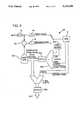
- FIG. 2is a block diagram of a dithered residue converter according to one embodiment of the present invention.
- a dithered residue converter 36uses basically the same apparatus as the prior art converter 10, but employs a different methodology.
- the crux of the differenceis that the noise source 28a produces noise words of sufficiently fine resolution that the second pass conversion from the ADC 18 does not always change with a change in the least significant bits of the dither word.
- the resolution of the DAC 20ais extended from 13 bits to 16, but the resolution of the ADC 18 remains at 8 bits.
- the dither wordcomprises nine bits.
- the accumulators 24a, 30a and latches 32a, 26aare 16-bit devices to accommodate the enhanced resolution provided by the illustrated form of the invention.
- the first pass output from the 8-bit ADC 18is justified into the eight most significant bits of the accumulator 30.
- a nine bit noise wordis justified into the least significant bits of this accumulator. As in the FIG. 1 system, the most significant of the noise word overlaps with the least significant bit of the first pass conversion in this accumulator. The remaining eight bits of the noise word do not overlap.
- the resultant 16-bit wordis loaded into the latch 32a and the output accumulator 24a.
- the 16-bit word latched into the latch 32ais converted into analog form by the 16-bit DAC 20a.
- the residue signal output by the difference circuit 22is again amplified by a factor of 32 (relative to the first pass). Accordingly, the five most significant non-overlapped bits of the dither word are amplified in significance to the point that they fall within the 8-bit resolution of the ADC 18 in the second pass.
- the three least significant bits of the noise wordeven after this amplification, still are insufficient to always toggle even the least significant bit of the converter 18 in the second pass conversion. These three bits, however, bias the result of the second pass ADC conversion, allowing the whole converter to resolve smaller levels than one count of the second pass ADC conversion when the three new dither bits are added in, as detailed below.
- the 8-bit word produced by the ADC 18 in the second passis loaded into the output accumulator 24a.
- this second pass wordis not justified into the accumulator's least significant bits. Rather, this word is offset from the accumulator's least significant bit by the number of noise bits that are insufficient to toggle the ADC 18. In the illustrated system, there are three such bits, so the least significant bit of the second pass conversion is justified into the accumulator so that its least significant bit is aligned with the accumulator's fourth least significant bit.
- the next lower increment of the 13 bit conversionwould be 0000000000000000, extended to 16 bits, so the input is only bracketed between 0 and 8, 13 bit resolution.
- a special caseis when the dither is 001. Subtracting the dither (of value 1) from the input signal (of value 9) results in an ADC input of value 8, which is exactly one count of the ADC. This places the ADC exactly on the threshold of the 00000000 to 00000001 transition. Since either ADC state is equally likely, the foregoing table reflects 1/16 probability for each value. If the dither is greater than one count, then the ADC sees an input of less than a value of 8 and so always produces a conversion of 00000000. (A larger dither corresponds to a smaller residue due to the signal path through the analog difference circuit 22.) If the dither is less than one of its counts, then the ADC sees an input greater than a value of 8 and so always produces 00000001.
- the average output codeis 5. This is biased 4 counts (1/2 count of the second pass ADC conversion) below the actual input, equivalent to 9 counts. (If the equivalent input had been 12, the average would have been 8, etc.) Since this bias is fixed, it can be subtracted out if needed.
- the output codeis greater than 5 as much as it is less than 5. Consequently, a check of this converter with a tracking loop to determine the input threshold for each of its 16-bit output codes yields results that are indistinguishable from those produced with a conventional 16-bit converter.
- N 1be the resolution of the ADC 18 on the first pass
- N 2be the resolution of the ADC 18 on the second pass
- Kbe the first pass analog scaling factor
- Mthe number of bits in the digital noise words
- Pbe the number of bits in the composite first pass/dither word (and, in this example, the number of bits in the final output word);
- the number of bits, X, of the M-bit noise word that are too fine to be reflected in the second pass output of the ADC 18can be computed as follows:
- the present inventionmay be characterized as any in which the value of X is greater than 0.
- the value of Xis three, indicating that three bits of the noise word are too finely resolved to be reflected in the second pass output of the ADC 18.
- 16-bit accuracycan be obtained with an 8-bit ADC without sacrificing the error correcting benefits of dither.
Landscapes
- Engineering & Computer Science (AREA)
- Theoretical Computer Science (AREA)
- Analogue/Digital Conversion (AREA)
Abstract
Description
TABLE I ______________________________________ com- DAC Prob- Output pared LSBs ADC ability Code counts to 5 ______________________________________ 000 00000001 1/8 0000000000001000 8 > 001 00000001 1/16 0000000000001001 9 > 001 00000000 1/16 0000000000000001 1 < 010 00000000 1/8 0000000000000010 2 < 011 00000000 1/8 0000000000000011 3 < 100 00000000 1/8 0000000000000100 4 < 101 00000000 1/8 0000000000000101 5 = 110 00000000 1/8 0000000000000110 6 > 111 00000000 1/8 0000000000000111 7 > probability weighted average = 5 ______________________________________
X=P-N.sub.2 -log.sub.2 (L/K)
TABLE II ______________________________________PRIOR ART CONVERTER 36 ______________________________________ N.sub.1 8 8 N.sub.2 8 8 K .125 .125 L 4 4M 6 9P 13 16 X 0 3 ______________________________________
Claims (10)
X=P-N.sub.2 -log.sub.2 (L/K), and X≧1.
P-N-log.sub.2 (L/K)≦1.
Priority Applications (2)
| Application Number | Priority Date | Filing Date | Title |
|---|---|---|---|
| US07/593,441US5134399A (en) | 1990-10-05 | 1990-10-05 | Subranging analog-to-digital converter with dither |
| US07/817,710US5187481A (en) | 1990-10-05 | 1992-01-07 | Combined and simplified multiplexing and dithered analog to digital converter |
Applications Claiming Priority (1)
| Application Number | Priority Date | Filing Date | Title |
|---|---|---|---|
| US07/593,441US5134399A (en) | 1990-10-05 | 1990-10-05 | Subranging analog-to-digital converter with dither |
Related Child Applications (1)
| Application Number | Title | Priority Date | Filing Date |
|---|---|---|---|
| US07/817,710Continuation-In-PartUS5187481A (en) | 1990-10-05 | 1992-01-07 | Combined and simplified multiplexing and dithered analog to digital converter |
Publications (1)
| Publication Number | Publication Date |
|---|---|
| US5134399Atrue US5134399A (en) | 1992-07-28 |
Family
ID=24374725
Family Applications (1)
| Application Number | Title | Priority Date | Filing Date |
|---|---|---|---|
| US07/593,441Expired - LifetimeUS5134399A (en) | 1990-10-05 | 1990-10-05 | Subranging analog-to-digital converter with dither |
Country Status (1)
| Country | Link |
|---|---|
| US (1) | US5134399A (en) |
Cited By (14)
| Publication number | Priority date | Publication date | Assignee | Title |
|---|---|---|---|---|
| US5189418A (en)* | 1992-04-16 | 1993-02-23 | Hewlett-Packard Company | Dither error correction |
| US5250948A (en)* | 1991-12-19 | 1993-10-05 | Eastman Kodak Company | High level resolution enhancement for dual-range A/D conversion |
| US5483238A (en)* | 1993-12-16 | 1996-01-09 | At&T Ipm Corp. | Data converter with gain scaling including dither |
| US5493298A (en)* | 1993-03-01 | 1996-02-20 | Hewlett-Packard Company | Dithered analog-to-digital converter |
| US5629703A (en)* | 1995-08-09 | 1997-05-13 | Tektronix, Inc. | Method for reducing harmonic distortion in an analog-to-digital converter system |
| FR2741213A1 (en)* | 1995-11-13 | 1997-05-16 | Valeo Electronique | Analog=digital converter for car temperature control |
| US5680870A (en)* | 1995-01-04 | 1997-10-28 | Johnson & Johnson Medical, Inc. | Oscillometric blood pressure monitor which acquires blood pressure signals from composite arterial pulse signal |
| US5717396A (en)* | 1996-06-17 | 1998-02-10 | Lucent Technologies Inc. | Analog-to-digital converter signal storage capacitor perturbation |
| US5731775A (en)* | 1996-06-17 | 1998-03-24 | Lucent Technologies Inc. | Subranging converter with plurality of resistor strings and transistor switches |
| US5990815A (en)* | 1997-09-30 | 1999-11-23 | Raytheon Company | Monolithic circuit and method for adding a randomized dither signal to the fine quantizer element of a subranging analog-to digital converter (ADC) |
| US6014097A (en)* | 1998-09-30 | 2000-01-11 | National Semiconductor Corporation | Fully differential interpolating comparator bank and method |
| US20060022854A1 (en)* | 2004-07-29 | 2006-02-02 | Johnny Bjornsen | Method and apparatus for operating correlator of an ADC circuit |
| US20190245550A1 (en)* | 2018-02-02 | 2019-08-08 | Analog Devices, Inc. | Background calibration of non-linearity of samplers and amplifiers in adcs |
| US20220263645A1 (en)* | 2019-07-25 | 2022-08-18 | Nippon Telegraph And Telephone Corporation | Synchronous detection apparatus, synchronous detection method, and program |
Citations (3)
| Publication number | Priority date | Publication date | Assignee | Title |
|---|---|---|---|---|
| US4550309A (en)* | 1984-02-16 | 1985-10-29 | Hewlett Packard Company | Analog to digital converter |
| US4814767A (en)* | 1987-10-08 | 1989-03-21 | Analog Devices, Inc. | Sub-ranging A/D converter with flash converter having balanced input |
| US4903023A (en)* | 1985-11-06 | 1990-02-20 | Westinghouse Electric Corp. | Subranging analog-to-digital converter with digital error correction |
- 1990
- 1990-10-05USUS07/593,441patent/US5134399A/ennot_activeExpired - Lifetime
Patent Citations (3)
| Publication number | Priority date | Publication date | Assignee | Title |
|---|---|---|---|---|
| US4550309A (en)* | 1984-02-16 | 1985-10-29 | Hewlett Packard Company | Analog to digital converter |
| US4903023A (en)* | 1985-11-06 | 1990-02-20 | Westinghouse Electric Corp. | Subranging analog-to-digital converter with digital error correction |
| US4814767A (en)* | 1987-10-08 | 1989-03-21 | Analog Devices, Inc. | Sub-ranging A/D converter with flash converter having balanced input |
Cited By (20)
| Publication number | Priority date | Publication date | Assignee | Title |
|---|---|---|---|---|
| US5250948A (en)* | 1991-12-19 | 1993-10-05 | Eastman Kodak Company | High level resolution enhancement for dual-range A/D conversion |
| US5189418A (en)* | 1992-04-16 | 1993-02-23 | Hewlett-Packard Company | Dither error correction |
| US5493298A (en)* | 1993-03-01 | 1996-02-20 | Hewlett-Packard Company | Dithered analog-to-digital converter |
| US5483238A (en)* | 1993-12-16 | 1996-01-09 | At&T Ipm Corp. | Data converter with gain scaling including dither |
| US5680870A (en)* | 1995-01-04 | 1997-10-28 | Johnson & Johnson Medical, Inc. | Oscillometric blood pressure monitor which acquires blood pressure signals from composite arterial pulse signal |
| US5629703A (en)* | 1995-08-09 | 1997-05-13 | Tektronix, Inc. | Method for reducing harmonic distortion in an analog-to-digital converter system |
| FR2741213A1 (en)* | 1995-11-13 | 1997-05-16 | Valeo Electronique | Analog=digital converter for car temperature control |
| US5717396A (en)* | 1996-06-17 | 1998-02-10 | Lucent Technologies Inc. | Analog-to-digital converter signal storage capacitor perturbation |
| US5731775A (en)* | 1996-06-17 | 1998-03-24 | Lucent Technologies Inc. | Subranging converter with plurality of resistor strings and transistor switches |
| US5990815A (en)* | 1997-09-30 | 1999-11-23 | Raytheon Company | Monolithic circuit and method for adding a randomized dither signal to the fine quantizer element of a subranging analog-to digital converter (ADC) |
| US6014097A (en)* | 1998-09-30 | 2000-01-11 | National Semiconductor Corporation | Fully differential interpolating comparator bank and method |
| US6104332A (en)* | 1998-09-30 | 2000-08-15 | National Semiconductor Corporation | Absolute value circuit and method |
| US6121912A (en)* | 1998-09-30 | 2000-09-19 | National Semiconductor Corporation | Subranging analog-to-digital converter and method |
| US20060022854A1 (en)* | 2004-07-29 | 2006-02-02 | Johnny Bjornsen | Method and apparatus for operating correlator of an ADC circuit |
| US20190245550A1 (en)* | 2018-02-02 | 2019-08-08 | Analog Devices, Inc. | Background calibration of non-linearity of samplers and amplifiers in adcs |
| CN110138385A (en)* | 2018-02-02 | 2019-08-16 | 美国亚德诺半导体公司 | The background calibration of sampler and amplifier nonlinearity in ADC |
| US10659069B2 (en)* | 2018-02-02 | 2020-05-19 | Analog Devices, Inc. | Background calibration of non-linearity of samplers and amplifiers in ADCs |
| CN110138385B (en)* | 2018-02-02 | 2023-11-03 | 美国亚德诺半导体公司 | Non-linear background calibration of samplers and amplifiers in an ADC |
| US20220263645A1 (en)* | 2019-07-25 | 2022-08-18 | Nippon Telegraph And Telephone Corporation | Synchronous detection apparatus, synchronous detection method, and program |
| US11711198B2 (en)* | 2019-07-25 | 2023-07-25 | Nippon Telegraph And Telephone Corporation | Synchronous detection apparatus, synchronous detection method, and program |
Similar Documents
| Publication | Publication Date | Title |
|---|---|---|
| KR970005828B1 (en) | Multiple analog/digital converter for pipeline structure | |
| US5134399A (en) | Subranging analog-to-digital converter with dither | |
| US4415882A (en) | Analog to digital converter | |
| US5668549A (en) | Radix 2 architecture and calibration technique for pipelined analog to digital converters | |
| JP2819006B2 (en) | Thermometer binary encoding method | |
| EP1131888B1 (en) | Method of calibrating an analog-to-digital converter, and a calibration equipment | |
| US5043732A (en) | Analog-to-digital converter employing a pipeline multi-stage architecture | |
| US20070052573A1 (en) | Pipeline ADC with Minimum Overhead Digital Error Correction | |
| US5463395A (en) | Semi-flash type A/D converter employing a correction encoder for eliminating errors in the output signals due to noise, and a corresponding method therefor | |
| US5353027A (en) | Multistep analog-to-digital converter with error correction | |
| US8564469B2 (en) | Pipelined analog digital convertor | |
| US6285309B1 (en) | Nested pipelined analog-to-digital converter | |
| US5926123A (en) | Self calibration circuitry and algorithm for multipass analog to digital converter interstage gain correction | |
| CN111585574B (en) | Pipeline analog-to-digital converter | |
| US7209068B1 (en) | Analog to digital converter elements and methods for using such | |
| US6825783B2 (en) | Multi-stage analog-to-digital converter with pipeline structure and method for coding the same | |
| US8749412B1 (en) | Anti-noise successive approximation analog to digital conversion method | |
| US6124820A (en) | Error correction architecture for pipeline analog to digital converters | |
| US5623265A (en) | Flash analog-to-digital converter and method of operation | |
| US5977894A (en) | Digital calibration for analog-to-digital converters with implicit gain proration | |
| US5739781A (en) | Sub-ranging analog-to-digital converter with open-loop differential amplifiers | |
| US8487792B2 (en) | Method of gain calibration of an ADC stage and an ADC stage | |
| US11025262B1 (en) | Pipelined analog-to-digital converter | |
| CN118018021A (en) | A foreground calibration system and implementation method for pipeline ADC | |
| US20060114140A1 (en) | Two step flash analog to digital converter |
Legal Events
| Date | Code | Title | Description |
|---|---|---|---|
| AS | Assignment | Owner name:HEWLETT-PACKARD COMPANY, PALO ALTO, CA A CORP. OF Free format text:ASSIGNMENT OF ASSIGNORS INTEREST.;ASSIGNOR:HILLER, DONALD R.;REEL/FRAME:005552/0021 Effective date:19900911 | |
| STCF | Information on status: patent grant | Free format text:PATENTED CASE | |
| FEPP | Fee payment procedure | Free format text:PAYOR NUMBER ASSIGNED (ORIGINAL EVENT CODE: ASPN); ENTITY STATUS OF PATENT OWNER: LARGE ENTITY | |
| FPAY | Fee payment | Year of fee payment:4 | |
| FPAY | Fee payment | Year of fee payment:8 | |
| AS | Assignment | Owner name:HEWLETT-PACKARD COMPANY, A DELAWARE CORPORATION, C Free format text:MERGER;ASSIGNOR:HEWLETT-PACKARD COMPANY, A CALIFORNIA CORPORATION;REEL/FRAME:010841/0649 Effective date:19980520 | |
| AS | Assignment | Owner name:AGILENT TECHNOLOGIES INC., CALIFORNIA Free format text:ASSIGNMENT OF ASSIGNORS INTEREST;ASSIGNOR:HEWLETT-PACKARD COMPANY, A DELAWARE CORPORATION;REEL/FRAME:010901/0336 Effective date:20000520 | |
| FPAY | Fee payment | Year of fee payment:12 |