US5130275A - Post fabrication processing of semiconductor chips - Google Patents
Post fabrication processing of semiconductor chipsDownload PDFInfo
- Publication number
- US5130275A US5130275AUS07/547,652US54765290AUS5130275AUS 5130275 AUS5130275 AUS 5130275AUS 54765290 AUS54765290 AUS 54765290AUS 5130275 AUS5130275 AUS 5130275A
- Authority
- US
- United States
- Prior art keywords
- bumps
- semiconductor device
- pattern
- walls
- electrically conductive
- Prior art date
- Legal status (The legal status is an assumption and is not a legal conclusion. Google has not performed a legal analysis and makes no representation as to the accuracy of the status listed.)
- Expired - Lifetime
Links
Images


Classifications
- H—ELECTRICITY
- H01—ELECTRIC ELEMENTS
- H01L—SEMICONDUCTOR DEVICES NOT COVERED BY CLASS H10
- H01L24/00—Arrangements for connecting or disconnecting semiconductor or solid-state bodies; Methods or apparatus related thereto
- H01L24/01—Means for bonding being attached to, or being formed on, the surface to be connected, e.g. chip-to-package, die-attach, "first-level" interconnects; Manufacturing methods related thereto
- H01L24/10—Bump connectors ; Manufacturing methods related thereto
- H01L24/12—Structure, shape, material or disposition of the bump connectors prior to the connecting process
- C—CHEMISTRY; METALLURGY
- C23—COATING METALLIC MATERIAL; COATING MATERIAL WITH METALLIC MATERIAL; CHEMICAL SURFACE TREATMENT; DIFFUSION TREATMENT OF METALLIC MATERIAL; COATING BY VACUUM EVAPORATION, BY SPUTTERING, BY ION IMPLANTATION OR BY CHEMICAL VAPOUR DEPOSITION, IN GENERAL; INHIBITING CORROSION OF METALLIC MATERIAL OR INCRUSTATION IN GENERAL
- C23F—NON-MECHANICAL REMOVAL OF METALLIC MATERIAL FROM SURFACE; INHIBITING CORROSION OF METALLIC MATERIAL OR INCRUSTATION IN GENERAL; MULTI-STEP PROCESSES FOR SURFACE TREATMENT OF METALLIC MATERIAL INVOLVING AT LEAST ONE PROCESS PROVIDED FOR IN CLASS C23 AND AT LEAST ONE PROCESS COVERED BY SUBCLASS C21D OR C22F OR CLASS C25
- C23F1/00—Etching metallic material by chemical means
- C23F1/10—Etching compositions
- C23F1/14—Aqueous compositions
- C23F1/32—Alkaline compositions
- C23F1/38—Alkaline compositions for etching refractory metals
- H—ELECTRICITY
- H01—ELECTRIC ELEMENTS
- H01L—SEMICONDUCTOR DEVICES NOT COVERED BY CLASS H10
- H01L24/00—Arrangements for connecting or disconnecting semiconductor or solid-state bodies; Methods or apparatus related thereto
- H01L24/01—Means for bonding being attached to, or being formed on, the surface to be connected, e.g. chip-to-package, die-attach, "first-level" interconnects; Manufacturing methods related thereto
- H01L24/02—Bonding areas ; Manufacturing methods related thereto
- H01L24/03—Manufacturing methods
- H—ELECTRICITY
- H01—ELECTRIC ELEMENTS
- H01L—SEMICONDUCTOR DEVICES NOT COVERED BY CLASS H10
- H01L24/00—Arrangements for connecting or disconnecting semiconductor or solid-state bodies; Methods or apparatus related thereto
- H01L24/01—Means for bonding being attached to, or being formed on, the surface to be connected, e.g. chip-to-package, die-attach, "first-level" interconnects; Manufacturing methods related thereto
- H01L24/10—Bump connectors ; Manufacturing methods related thereto
- H01L24/11—Manufacturing methods
- H—ELECTRICITY
- H01—ELECTRIC ELEMENTS
- H01L—SEMICONDUCTOR DEVICES NOT COVERED BY CLASS H10
- H01L24/00—Arrangements for connecting or disconnecting semiconductor or solid-state bodies; Methods or apparatus related thereto
- H01L24/01—Means for bonding being attached to, or being formed on, the surface to be connected, e.g. chip-to-package, die-attach, "first-level" interconnects; Manufacturing methods related thereto
- H01L24/10—Bump connectors ; Manufacturing methods related thereto
- H01L24/15—Structure, shape, material or disposition of the bump connectors after the connecting process
- H01L24/16—Structure, shape, material or disposition of the bump connectors after the connecting process of an individual bump connector
- H—ELECTRICITY
- H01—ELECTRIC ELEMENTS
- H01L—SEMICONDUCTOR DEVICES NOT COVERED BY CLASS H10
- H01L2224/00—Indexing scheme for arrangements for connecting or disconnecting semiconductor or solid-state bodies and methods related thereto as covered by H01L24/00
- H01L2224/01—Means for bonding being attached to, or being formed on, the surface to be connected, e.g. chip-to-package, die-attach, "first-level" interconnects; Manufacturing methods related thereto
- H01L2224/02—Bonding areas; Manufacturing methods related thereto
- H01L2224/03—Manufacturing methods
- H01L2224/0347—Manufacturing methods using a lift-off mask
- H—ELECTRICITY
- H01—ELECTRIC ELEMENTS
- H01L—SEMICONDUCTOR DEVICES NOT COVERED BY CLASS H10
- H01L2224/00—Indexing scheme for arrangements for connecting or disconnecting semiconductor or solid-state bodies and methods related thereto as covered by H01L24/00
- H01L2224/01—Means for bonding being attached to, or being formed on, the surface to be connected, e.g. chip-to-package, die-attach, "first-level" interconnects; Manufacturing methods related thereto
- H01L2224/02—Bonding areas; Manufacturing methods related thereto
- H01L2224/03—Manufacturing methods
- H01L2224/036—Manufacturing methods by patterning a pre-deposited material
- H01L2224/0361—Physical or chemical etching
- H—ELECTRICITY
- H01—ELECTRIC ELEMENTS
- H01L—SEMICONDUCTOR DEVICES NOT COVERED BY CLASS H10
- H01L2224/00—Indexing scheme for arrangements for connecting or disconnecting semiconductor or solid-state bodies and methods related thereto as covered by H01L24/00
- H01L2224/01—Means for bonding being attached to, or being formed on, the surface to be connected, e.g. chip-to-package, die-attach, "first-level" interconnects; Manufacturing methods related thereto
- H01L2224/02—Bonding areas; Manufacturing methods related thereto
- H01L2224/03—Manufacturing methods
- H01L2224/039—Methods of manufacturing bonding areas involving a specific sequence of method steps
- H01L2224/03912—Methods of manufacturing bonding areas involving a specific sequence of method steps the bump being used as a mask for patterning the bonding area
- H—ELECTRICITY
- H01—ELECTRIC ELEMENTS
- H01L—SEMICONDUCTOR DEVICES NOT COVERED BY CLASS H10
- H01L2224/00—Indexing scheme for arrangements for connecting or disconnecting semiconductor or solid-state bodies and methods related thereto as covered by H01L24/00
- H01L2224/01—Means for bonding being attached to, or being formed on, the surface to be connected, e.g. chip-to-package, die-attach, "first-level" interconnects; Manufacturing methods related thereto
- H01L2224/02—Bonding areas; Manufacturing methods related thereto
- H01L2224/04—Structure, shape, material or disposition of the bonding areas prior to the connecting process
- H01L2224/0401—Bonding areas specifically adapted for bump connectors, e.g. under bump metallisation [UBM]
- H—ELECTRICITY
- H01—ELECTRIC ELEMENTS
- H01L—SEMICONDUCTOR DEVICES NOT COVERED BY CLASS H10
- H01L2224/00—Indexing scheme for arrangements for connecting or disconnecting semiconductor or solid-state bodies and methods related thereto as covered by H01L24/00
- H01L2224/01—Means for bonding being attached to, or being formed on, the surface to be connected, e.g. chip-to-package, die-attach, "first-level" interconnects; Manufacturing methods related thereto
- H01L2224/10—Bump connectors; Manufacturing methods related thereto
- H01L2224/11—Manufacturing methods
- H01L2224/1147—Manufacturing methods using a lift-off mask
- H—ELECTRICITY
- H01—ELECTRIC ELEMENTS
- H01L—SEMICONDUCTOR DEVICES NOT COVERED BY CLASS H10
- H01L2224/00—Indexing scheme for arrangements for connecting or disconnecting semiconductor or solid-state bodies and methods related thereto as covered by H01L24/00
- H01L2224/01—Means for bonding being attached to, or being formed on, the surface to be connected, e.g. chip-to-package, die-attach, "first-level" interconnects; Manufacturing methods related thereto
- H01L2224/10—Bump connectors; Manufacturing methods related thereto
- H01L2224/11—Manufacturing methods
- H01L2224/119—Methods of manufacturing bump connectors involving a specific sequence of method steps
- H01L2224/11901—Methods of manufacturing bump connectors involving a specific sequence of method steps with repetition of the same manufacturing step
- H01L2224/11902—Multiple masking steps
- H01L2224/11903—Multiple masking steps using different masks
- H—ELECTRICITY
- H01—ELECTRIC ELEMENTS
- H01L—SEMICONDUCTOR DEVICES NOT COVERED BY CLASS H10
- H01L2224/00—Indexing scheme for arrangements for connecting or disconnecting semiconductor or solid-state bodies and methods related thereto as covered by H01L24/00
- H01L2224/01—Means for bonding being attached to, or being formed on, the surface to be connected, e.g. chip-to-package, die-attach, "first-level" interconnects; Manufacturing methods related thereto
- H01L2224/10—Bump connectors; Manufacturing methods related thereto
- H01L2224/12—Structure, shape, material or disposition of the bump connectors prior to the connecting process
- H01L2224/13—Structure, shape, material or disposition of the bump connectors prior to the connecting process of an individual bump connector
- H01L2224/13001—Core members of the bump connector
- H01L2224/1301—Shape
- H01L2224/13016—Shape in side view
- H01L2224/13018—Shape in side view comprising protrusions or indentations
- H01L2224/13019—Shape in side view comprising protrusions or indentations at the bonding interface of the bump connector, i.e. on the surface of the bump connector
- H—ELECTRICITY
- H01—ELECTRIC ELEMENTS
- H01L—SEMICONDUCTOR DEVICES NOT COVERED BY CLASS H10
- H01L2224/00—Indexing scheme for arrangements for connecting or disconnecting semiconductor or solid-state bodies and methods related thereto as covered by H01L24/00
- H01L2224/01—Means for bonding being attached to, or being formed on, the surface to be connected, e.g. chip-to-package, die-attach, "first-level" interconnects; Manufacturing methods related thereto
- H01L2224/10—Bump connectors; Manufacturing methods related thereto
- H01L2224/12—Structure, shape, material or disposition of the bump connectors prior to the connecting process
- H01L2224/13—Structure, shape, material or disposition of the bump connectors prior to the connecting process of an individual bump connector
- H01L2224/13001—Core members of the bump connector
- H01L2224/13075—Plural core members
- H01L2224/1308—Plural core members being stacked
- H—ELECTRICITY
- H01—ELECTRIC ELEMENTS
- H01L—SEMICONDUCTOR DEVICES NOT COVERED BY CLASS H10
- H01L2224/00—Indexing scheme for arrangements for connecting or disconnecting semiconductor or solid-state bodies and methods related thereto as covered by H01L24/00
- H01L2224/01—Means for bonding being attached to, or being formed on, the surface to be connected, e.g. chip-to-package, die-attach, "first-level" interconnects; Manufacturing methods related thereto
- H01L2224/10—Bump connectors; Manufacturing methods related thereto
- H01L2224/12—Structure, shape, material or disposition of the bump connectors prior to the connecting process
- H01L2224/13—Structure, shape, material or disposition of the bump connectors prior to the connecting process of an individual bump connector
- H01L2224/13001—Core members of the bump connector
- H01L2224/13099—Material
- H—ELECTRICITY
- H01—ELECTRIC ELEMENTS
- H01L—SEMICONDUCTOR DEVICES NOT COVERED BY CLASS H10
- H01L2924/00—Indexing scheme for arrangements or methods for connecting or disconnecting semiconductor or solid-state bodies as covered by H01L24/00
- H01L2924/01—Chemical elements
- H01L2924/01006—Carbon [C]
- H—ELECTRICITY
- H01—ELECTRIC ELEMENTS
- H01L—SEMICONDUCTOR DEVICES NOT COVERED BY CLASS H10
- H01L2924/00—Indexing scheme for arrangements or methods for connecting or disconnecting semiconductor or solid-state bodies as covered by H01L24/00
- H01L2924/01—Chemical elements
- H01L2924/01012—Magnesium [Mg]
- H—ELECTRICITY
- H01—ELECTRIC ELEMENTS
- H01L—SEMICONDUCTOR DEVICES NOT COVERED BY CLASS H10
- H01L2924/00—Indexing scheme for arrangements or methods for connecting or disconnecting semiconductor or solid-state bodies as covered by H01L24/00
- H01L2924/01—Chemical elements
- H01L2924/01013—Aluminum [Al]
- H—ELECTRICITY
- H01—ELECTRIC ELEMENTS
- H01L—SEMICONDUCTOR DEVICES NOT COVERED BY CLASS H10
- H01L2924/00—Indexing scheme for arrangements or methods for connecting or disconnecting semiconductor or solid-state bodies as covered by H01L24/00
- H01L2924/01—Chemical elements
- H01L2924/01014—Silicon [Si]
- H—ELECTRICITY
- H01—ELECTRIC ELEMENTS
- H01L—SEMICONDUCTOR DEVICES NOT COVERED BY CLASS H10
- H01L2924/00—Indexing scheme for arrangements or methods for connecting or disconnecting semiconductor or solid-state bodies as covered by H01L24/00
- H01L2924/01—Chemical elements
- H01L2924/01019—Potassium [K]
- H—ELECTRICITY
- H01—ELECTRIC ELEMENTS
- H01L—SEMICONDUCTOR DEVICES NOT COVERED BY CLASS H10
- H01L2924/00—Indexing scheme for arrangements or methods for connecting or disconnecting semiconductor or solid-state bodies as covered by H01L24/00
- H01L2924/01—Chemical elements
- H01L2924/0102—Calcium [Ca]
- H—ELECTRICITY
- H01—ELECTRIC ELEMENTS
- H01L—SEMICONDUCTOR DEVICES NOT COVERED BY CLASS H10
- H01L2924/00—Indexing scheme for arrangements or methods for connecting or disconnecting semiconductor or solid-state bodies as covered by H01L24/00
- H01L2924/01—Chemical elements
- H01L2924/01022—Titanium [Ti]
- H—ELECTRICITY
- H01—ELECTRIC ELEMENTS
- H01L—SEMICONDUCTOR DEVICES NOT COVERED BY CLASS H10
- H01L2924/00—Indexing scheme for arrangements or methods for connecting or disconnecting semiconductor or solid-state bodies as covered by H01L24/00
- H01L2924/01—Chemical elements
- H01L2924/01024—Chromium [Cr]
- H—ELECTRICITY
- H01—ELECTRIC ELEMENTS
- H01L—SEMICONDUCTOR DEVICES NOT COVERED BY CLASS H10
- H01L2924/00—Indexing scheme for arrangements or methods for connecting or disconnecting semiconductor or solid-state bodies as covered by H01L24/00
- H01L2924/01—Chemical elements
- H01L2924/01029—Copper [Cu]
- H—ELECTRICITY
- H01—ELECTRIC ELEMENTS
- H01L—SEMICONDUCTOR DEVICES NOT COVERED BY CLASS H10
- H01L2924/00—Indexing scheme for arrangements or methods for connecting or disconnecting semiconductor or solid-state bodies as covered by H01L24/00
- H01L2924/01—Chemical elements
- H01L2924/0103—Zinc [Zn]
- H—ELECTRICITY
- H01—ELECTRIC ELEMENTS
- H01L—SEMICONDUCTOR DEVICES NOT COVERED BY CLASS H10
- H01L2924/00—Indexing scheme for arrangements or methods for connecting or disconnecting semiconductor or solid-state bodies as covered by H01L24/00
- H01L2924/01—Chemical elements
- H01L2924/01033—Arsenic [As]
- H—ELECTRICITY
- H01—ELECTRIC ELEMENTS
- H01L—SEMICONDUCTOR DEVICES NOT COVERED BY CLASS H10
- H01L2924/00—Indexing scheme for arrangements or methods for connecting or disconnecting semiconductor or solid-state bodies as covered by H01L24/00
- H01L2924/01—Chemical elements
- H01L2924/0105—Tin [Sn]
- H—ELECTRICITY
- H01—ELECTRIC ELEMENTS
- H01L—SEMICONDUCTOR DEVICES NOT COVERED BY CLASS H10
- H01L2924/00—Indexing scheme for arrangements or methods for connecting or disconnecting semiconductor or solid-state bodies as covered by H01L24/00
- H01L2924/01—Chemical elements
- H01L2924/01074—Tungsten [W]
- H—ELECTRICITY
- H01—ELECTRIC ELEMENTS
- H01L—SEMICONDUCTOR DEVICES NOT COVERED BY CLASS H10
- H01L2924/00—Indexing scheme for arrangements or methods for connecting or disconnecting semiconductor or solid-state bodies as covered by H01L24/00
- H01L2924/01—Chemical elements
- H01L2924/01079—Gold [Au]
- H—ELECTRICITY
- H01—ELECTRIC ELEMENTS
- H01L—SEMICONDUCTOR DEVICES NOT COVERED BY CLASS H10
- H01L2924/00—Indexing scheme for arrangements or methods for connecting or disconnecting semiconductor or solid-state bodies as covered by H01L24/00
- H01L2924/01—Chemical elements
- H01L2924/01082—Lead [Pb]
- H—ELECTRICITY
- H01—ELECTRIC ELEMENTS
- H01L—SEMICONDUCTOR DEVICES NOT COVERED BY CLASS H10
- H01L2924/00—Indexing scheme for arrangements or methods for connecting or disconnecting semiconductor or solid-state bodies as covered by H01L24/00
- H01L2924/013—Alloys
- H01L2924/0132—Binary Alloys
- H01L2924/01327—Intermediate phases, i.e. intermetallics compounds
- H—ELECTRICITY
- H01—ELECTRIC ELEMENTS
- H01L—SEMICONDUCTOR DEVICES NOT COVERED BY CLASS H10
- H01L2924/00—Indexing scheme for arrangements or methods for connecting or disconnecting semiconductor or solid-state bodies as covered by H01L24/00
- H01L2924/013—Alloys
- H01L2924/014—Solder alloys
- H—ELECTRICITY
- H01—ELECTRIC ELEMENTS
- H01L—SEMICONDUCTOR DEVICES NOT COVERED BY CLASS H10
- H01L2924/00—Indexing scheme for arrangements or methods for connecting or disconnecting semiconductor or solid-state bodies as covered by H01L24/00
- H01L2924/10—Details of semiconductor or other solid state devices to be connected
- H01L2924/11—Device type
- H01L2924/14—Integrated circuits
Definitions
- This inventionrelates to the post fabrication processing of semiconductor chips. After circuits are patterned on semiconductor wafers, and the wafers are separated into individual chips in the chip fabrication process, a number of steps are done to prepare the chip for use in a piece of electronic equipment, such as a computer.
- the semiconductor devicesIn order to communicate data with the piece of electronic equipment, the semiconductor devices must be electrically connected to the piece of electronic equipment, most commonly by electrically and mechanically attaching the semiconductor device to a circuit board. This interconnection is typically done by attaching the semiconductor device to electrical leads, which are then attached to the circuit board, or by attaching the semiconductor device to a substrate, which is then attached to a circuit board.
- Bumpsare portions of conductive material placed on the interconnect pads of semiconductor devices. Since interconnect pads are commonly placed on an axis of alignment parallel and proximate to each edge of the semiconductor device, the bumps are situated in a similar pattern. Bumps serve as both conductive paths and mechanical standoffs. A discussion of bumps is contained in U.S. Pat. No. 4,510,017, issued on Apr. 9, 1985 to Barber.
- intermetallicsare materials formed at the interface between two metals by the diffusion of one metal into the other. The degree to which intermetallics form is dependent on a number of properties of the two metals.
- Intermetallicsmay have undesirable electrical properties, such as poor or unpredictable conductivity, or undesirable mechanical properties, such as brittleness.
- Aluminumis a common choice for the interconnect pads and gold is a common material for the bumps. However, the combination of aluminum and gold is prone to the formation of intermetallics.
- a barrier metalis a metal that does not form harmful intermetallics with either of the two metals that would be in contact, but has desirable electrical and mechanical properties, such as high and predictable conductivity, ductility, and resistance to corrosion. Chromium and titanium tungsten alloy are common materials used for a barrier metal layer between gold and aluminum.
- the barrier metal layer metal layercan be added as a thin layer over the entire semiconductor device by a process such as sputtering. After further processing, the portion of the barrier metal layer, except the portion lying under the bumps is removed.
- a common material for removing a barrier layer composed of titanium tungsten alloyis a 30% solution of hydrogen peroxide in water.
- barrier metal materialssuch as titanium tungsten alloys
- the surface of the barrier metal layermay oxidize during subsequent processing steps. This oxide layer may prevent subsequent layers from adhering to the barrier layer. Therefore, a layer of another metal such as gold, which is not subject to oxidation, is sometimes applied immediately after the application of the barrier layer.
- the bump materialis gold
- the oxidization preventing layercan also serve as a base on which the gold bump can be built, and for that reason it is often referred to as a "seed layer".
- the bumpis formed, and the portion of the seed layer not lying under the bumps is removed by later processing.
- a common material for removing a gold seed layeris potassium cyanide.
- compression bondingis two common methods for accomplishing mechanical and electrical connection.
- An example of compression bondingcan be found in U.S. Pat. No. 4,000,842, issued Jan. 4, 1977 to Burns, and in U.S. Pat. No. 4,188,438, issued Feb. 12, 1980, also to Burns.
- Burns patentsboth specify a temperature of 550 degrees C. and a pressure of 100 grams per bump or 8 grams per square mil. Such high temperatures and pressures can damage the bumped device, the electrical leads, or the circuit board. Modern bumped devices may have as many as 600 bumps, which would require 60,000 grams of pressure according to the teaching of the Burns patents. This amount of force is sufficient to cause significant damage to semiconductor devices. Semiconductor devices are incapable of withstanding such pressure. The amount of pressure that must be applied at one time can be reduced by bonding only a portion of the bumps with each application of pressure. However, this results in a longer, more expensive manufacturing process, and may exposes the circuit board to the high temperature for a longer time.
- a bead of flowable metalsuch as tin or tin-lead solder, is applied to each bump.
- a typical method of applying the flowable metalis illustrated in U.S. Pat. No. 3,625,837, issued Dec. 7, 1971 to Nelson et al.
- Nelson et al.a calcium magnesium aluminosilicate glass layer is formed over the semiconductor device by a sputtering process. The portion of glass layer over the terminal areas is then etched away.
- layers of chromium and copperare deposited on the entire semiconductor device.
- a maskis then formed over the semiconductor device using photoresist and photographic techniques to leave an opening in the photoresist layer that is slightly larger than the openings below them in the glass layer.
- solderis then applied to the openings using electrodeposition.
- the portion of the copper and chromium layers that are exposed, that is that do not lie under the solder,are then removed by a suitable etchant. Heat is then applied, which causes the solder to form rounded bumps.
- nominal bump spacingIn recent years, the number of bumps on each chip has increased. One result has been that the nominal distance between the adjacent edges of adjacent bumps (hereinafter referred to as "nominal bump spacing") has decreased. In a typical modern semiconductor device, the nominal bump spacing is 0.006 in. (0.1524 mm), with some devices having a nominal bump spacing of 0.004 in. (0.1016 mm).
- Tin whiskeringis the propensity of metals such as tin to grow thin crystals projecting outward from the portions of solder on the bumps. Tin whiskers tend to grow in the same direction as the crystals of the hardened solder. Tin whiskering is discussed in more detail in the article "A Model for the Spontaneous Growth of Zinc, Cadmium, and Tin Whiskers", by U. Lindborg, published on pages 181 through 186 in Acta Metallurgica, Vol. 24 (Pergamon Press, 1976).
- Tin whiskers growing on solder beads or on tin electronic leadsmay eventually grow long enough that they touch the adjacent solder bead or the adjacent electronic lead or they may touch a tin whisker growing from an adjacent solder bead or electronic lead. This can result in an electrical short circuit. Electrical short circuits caused by tin whiskers are particularly troublesome, because it is difficult to predict where and when they will occur.
- Semiconductor chipsare normally processed such that the circuitry is patterned on only one side of the substrate.
- the side on which the circuitry is patternedis called the active side of the substrate.
- the other side of the chipis called the passive side or the backside of the substrate.
- Chip performancecan be improved by processing the passive side of the substrate.
- Two operations that are often done to the passive side of the substrateare thinning and depositing a protective layer to the passive side of the substrate.
- Thinningis typically done by a lapping process in which an abrasive substance removes material from the passive side of the substrate.
- Thinningmay also be done by the action of chemicals. This is typically done during the fabrication process. If it is done during the fabrication process, the active side of the semiconductor device needs to be protected from the chemical, which adds and extra process step.
- the material deposited on the passive side of the substrateis typically a conductor such as gold, and is typically deposited by electrodeposition.
- the post fabrication processing of bumped semiconductor devicesincludes the steps of placing a barrier metal layer on the interconnect pads of the semiconductor device; applying a seed layer on top of the barrier metal layer; depositing a bump on the portion of the seed layer which lie over the interconnect pads of the semiconductor device; depositing a solder bead over the exposed surfaces of the bump; optionally, depositing a coating on the passive side of the substrate; removing the portion of the seed layer which does not lie under the bumps; and removing the portion of the barrier metal layer with a 30% hydrogen peroxide solution.
- the active side of a semiconductor devicesuch as an integrated circuit chip which has interconnect pads on the active side, is first coated with a barrier metal layer, then a seed layer.
- a layer of photoresistis then applied to the active side of the semiconductor device, and an opening is formed in the photoresist layer on each of the interconnect pads of the device, using photolithography. Bumps are then deposited in the openings by electrodeposition.
- the semiconductor deviceis then made thinner, by removing material from the passive side of the semiconductor device. The material is removed by exposing the passive side to a chemical which dissolves the substance form which the substrate of the semiconductor device is made. The photoresist layer is then removed.
- a passive side coatingis desired, it is then applied and annealed.
- a layer of photoresistis formed on the active side of the device.
- An opening in the photoresist layeris then created over each bump using common photolithographic techniques.
- Each opening in the photoresist layeris 15 to 30% narrower than the bump on which it is placed, when measured along a line connecting the bump with the adjacent bump.
- Solderis then deposited in the openings in the photoresist layer using electrodeposition.
- the photoresist layeris then removed. If a coating has been deposited on the second side, it is then covered by a protective coating. The portions of the seed layer not lying under the solder bead is removed.
- the portion of the barrier metal layer not lying under the bumpare then removed from the active side of the semiconductor device using a peroxide solution, with sufficient hydroxide ions added to bring the pH to between 9 and 11.
- the protective layeris then removed from the passive side of the semiconductor device.
- the conductive padseach of which consists of an interconnect pad, a bump, and a solder bead, are then attached to a circuit board or to an electrical lead.
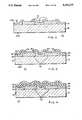
- FIG. 1is a perspective view of a semiconductor device as it comes from the semiconductor fabrication process.
- FIG. 2is a cross sectional view of a semiconductor device as it comes from the semiconductor fabrication process.
- FIGS. 3 through 16are cross sectional views of the semiconductor device at different stages of the sequential processing.
- FIGS. 17a and 17bare perspective views of a TAB lead attached to an electrically conductive pad made according to the invention.
- FIGS. 18a and 18bare cross sectional views of a semiconductor device with a conductive pad made according to the invention, attached to a pad on a substrate.
- FIG. 1shows the semiconductor device 10 which is manufactured by processes well known in the art.
- the semiconductor device 10consists of a substrate 12 on which is patterned the transistors and other elements (not shown), the power and signal paths interconnecting the transistors and other elements (not shown), and the power and signal paths (not shown) which terminate at interconnect pads 14.
- Substrate 12is generally rectangular or square, typically a piece of silicon approximately 0.019 inches (0.4826 mm) thick or gallium arsenide approximately 0.007 inches (0.1778 mm) thick and with sides 0.1 inches (2.54 mm) to 0.5 inches (16.129 mm) in width.
- the thickness of the substrate 12is the original thickness, as not thinning has yet been performed.
- the top and bottom surfacesare generally planar and parallel.
- Interconnect pads 14provide a point at which signals can be transmitted to and from the semiconductor device and at which power can be transmitted to the device.
- Interconnect pads 14are made of an electrically conductive material, typically aluminum or gold, and, when viewed from above, are usually square or round, but may be some other convenient shape. They are typically 100 microns across and between 1 and 3 microns thick. There may be over a hundred integrated circuit interconnect pads 14 on the semiconductor device 10. Interconnect pads 14 are normally aligned, with the axis of alignment parallel and proximate to the side 82 of the integrated circuit chip 10. There may be more than one row along an edge of the integrated circuit chip 10. In addition, other bump patterns are possible, with bumps placed at many points on the semiconductor device.
- the transistors and other elementsare on the active side 22a of the substrate 12. There are typically no transistors or elements on the passive side 22b of the substrate 12.
- Passivation layer 16which covers the active side 22a of the substrate 12 is a layer of an electrical insulator, such as silicon dioxide, that electrically isolates the integrated circuit chip 10 and protects the substrate 12 from damage during subsequent manufacturing steps.
- the passivation layer 16is formed as a part of the fabrication process of the semiconductor device 10.
- the thickness of the passivation layeris typically 2000 Angstrom Units.
- the barrier metal layer 18 of an alloy of 10% by weight titanium and 90% by weight tungstenis placed on the entire active side 22a of the substrate 12 immediately above the passivation layer 16 and the interconnect pads 14, as shown in FIG. 3.
- the barrier metal layer 18is a coating that is thin relative to the substrate 12. The coating is of a relatively uniform thickness.
- the bottom surface of the barrier metal layer 18conforms to the top surface of the passivation layer 16 and the interconnect pads 14.
- the top surface of barrier metal layer 18takes on a rounded shape 62 at corners 60 of the passivation layer 16 which are at approximately right angles.
- the nominal thickness of the barrier metal layer 18is typically 3000 to 7000 Angstrom units and can be deposited by a number of processes well known to the art, such as sputtering.
- FIG. 4shows the semiconductor device 10 after the deposition of the seed layer 26.
- Seed layer 26covers the entire barrier metal layer 18.
- Seed layer 26is a coating that is thin relative to the substrate 12, and is of a relatively uniform thickness.
- the top and bottom surfaces of seed layer 26conform to top surface of the barrier layer 18.
- Seed layer 26is often composed of the same material as the bump, but may be some other material. Common seed layer materials are copper or gold.
- Seed layer 26is normally between 1000 and 4000 Angstrom units thick and can be deposited by a number of processes familiar to the art, such as sputtering.
- Layer of photoresist 28is deposited on the seed layer 26.
- the bottom surface of photoresist layer 28conforms to the top surface of the seed layer 26 and the top surface of the the photoresist is relatively planar.
- the thickness of the photoresistis layer 28 at the location of the bump is greater than the thickness of the bump which is added in a subsequent step.
- a typical bump thicknessis 25 microns and a typical thickness bf a photoresist layer at the location of the bump is 35 microns.
- the photoresist layeris composed of materials well known to the art, and is deposited by spinning or spin casting.
- an opening 30is formed in the photoresist layer 28. Openings 30, when viewed from above are approximately the same shape as interconnect pads 14. The size of openings 30, when viewed from above is slightly smaller than the size of the interconnect pads 14, but slightly larger than the opening in the passivation layer 16.
- the photoresist layer 28serves as a mask to ensure that the bump material gets deposited on the bump location, but not at other areas of the semiconductor device 10.
- Bumps 34are then deposited into the holes 30 in the photoresist layer,resulting in a configuration as shown in FIG. 6.
- Bumps 34are typically composed of gold or copper, and are deposited by methods familiar to the art, such as electrodeposition.
- the edges 72 of the bumpsare defined by the walls 74 of the openings 30, which are approximately perpendicular to the plane of the active side 22a of the semiconductor device 10.
- the top surface of the bump 34conforms to the top surface of the seed layer 18.
- the bottom surface of the bump 34conforms to the top surface of seed layer 18.
- materialis removed from the passive side 22b of the substrate 12.
- the materialis removed uniformly, from the entire surface of the passive side 22b of the substrate 12, so that the passive side 22b of the substrate 12 remains planar.
- the materialis removed by exposing the passive side 22b to a chemical, such as a solution of 10% by volume reagent grade hydrofluoric acid and 90% by volume reagent grade nitric acid that dissolves the material of the substrate 12, typically silicon, but does not react with the photoresist layer 28 or the bumps 34.
- a chemicalsuch as a solution of 10% by volume reagent grade hydrofluoric acid and 90% by volume reagent grade nitric acid that dissolves the material of the substrate 12, typically silicon, but does not react with the photoresist layer 28 or the bumps 34.
- a mixture of these proportionswill normally remove 0.0001 in of semiconductor grade silicon per minute. Therefore, to accomplish a typical reduction of 0.003 in, the substrate 12 is exposed to the hydrogen peroxide and hydrofluoric acid solution for 30 minutes
- the photoresist layer 28 and the bumps 34protects the active side 22a of the substrate 12, no material is removed from the active side 22a of the substrate 12.
- the photoresist layer 28serves both as a mask for the deposition of the bumps and as a protective coating to prevent damage to the active side 22a of the substrate 12 while material is removed from the passive side 22b of the substrate 12.
- the remaining photoresistis removed by methods well known to the art, resulting in FIG. 8.
- the removal of the remaining photoresistexposes the bumps 34 and the portion of the seed layer 26 not lying under the bumps 34.
- passive side coating 36is now deposited, using a methods well known to the art, such as sputtering.
- the materialis deposited uniformly, so that both surfaces of the coating are generally planar and parallel to the passive side 22b of the substrate 12.
- Passive side coating 36is then annealed by exposing the semiconductor device 10 to a temperature of 350 to 400 degrees Celsius for a time of 20 to 30 minutes. The annealing aids the bonding of the passive side coating 36 to the passive side 22b, and repairs any damage to transistors that may have been caused by the sputtering process.
- the passive side coating 36is made of gold, and is 1000-3000 Angstrom units thick. This deposition of passive side coating 36 is optional. Subsequent drawings will show the coating 36, but those skilled in the art will recognize that subsequent steps in the process can be performed without coating 36.
- the next stepis a photolithography step that results in the configuration shown in FIG. 10.
- a photoresist layer 38is deposited on the seed layer 26 and the bumps 34.
- the bottom surface of photoresist layer 38conforms to the top surface of the seed layer 26 and the bumps 34.
- the top surface of photoresist layer 38is relatively planar.
- the photoresist layeris composed of materials well known to the art, and is deposited by spinning or spin casting.
- the thickness of photoresist layer 38 at the location of the solder beadis greater than the thickness of the solder bead to be applied subsequently to ensure that the solder beads are contained in the openings 40 and to allow for variations in the thickness of the photoresist.
- a typical solder bead thicknessis 4 microns and a typical photoresist layer thickness at the location of the photoresist is 35 microns.
- openings 40in the photoresist layer 38 which lie above the bumps 34.
- Openings 40when viewed from above are approximately the same shape of the bumps 34.
- the walls 46 of the openings 40are perpendicular to the plane of the top of the active side 22a of the substrate 12.
- the distance between opposite walls 46 of the openings 40, measured along a line connecting each wall 46 with the adjacent opening 40,is 15 to 30% less than the nominal width of the bumps 34, measured along the same line.
- Opening 40is situated such that the distance between the adjacent edges of adjacent bumps is less than the distance between adjacent walls of adjacent openings.
- the photoresist layer 38serves as a mask to ensure that the solder bead material gets deposited on the bump location, but not at other areas of the semiconductor device 10, and ensures that the solder bead 44 is narrower than the bump 44, when measured on a line connecting the bump with the adjacent bump.
- FIG. 11shows the semiconductor device 10 after the flowable alloy, in the preferred embodiment a solder bead 44 of tin, is deposited in the openings 40 in the photoresist layer 38 by methods well known to the art, such as electroplating.
- the thickness of the solder bead 44is dependent on the solder material. If the solder is tin, the thickness is typically 2 to 4 microns.
- the edges 94 of the solder bead 44are defined by the walls 46 of the openings 40.
- the top and bottom surfaces of the solder bead 44conform to the top of the bump 34 over which it lies. Therefore, the top and bottom surfaces of the solder bead 44 may slope upwardly as shown in the drawings, or may be planar, depending on the topology of the portion of the bump covered by the solder beads 44.
- the photoresist layeris then stripped away by methods well known to the art, exposing the solder bead 44, the portion of the bumps 34 not lying under the solder bead 44, and the portion of the seed layer 26 not lying under the bumps 34.
- the nominal width of the solder beadsis 15 to 30% less than the nominal width of the bumps 34.
- the nominal distance between the adjacent edges of adjacent solder beadsis greater than the nominal distance between the adjacent edges of adjacent bumps.
- a protective layer 46is applied over the entire surface of the passive side coating 36.
- the protective layer 46may be photoresist or a protective tape, and is typically uniform in thickness. This step may be omitted if application of passive side coating 36 has been omitted.
- FIG. 14shows the semiconductor device after the portion of the seed layer 26 not lying under a bump is etched away, exposing the portion of the barrier metal layer 18 not lying under one of the bumps 34.
- the seed layer 26is gold, it is removed by exposure to a 10% solution of Potassium Cyanide for 90 seconds. Since the bumps 44 are also gold, the potassium cyanide solution also attacks the bumps 44. However since the bumps 44 are 25 microns thick while the seed layer 26 is 0.3 microns thick, the amount of each bump that is removed is a small fraction of the bump.
- a typical etchantis a source of unstable oxygen, normally referred to as a peroxide.
- the most commonis a 30% solution of hydrogen peroxide in water.
- peroxidescan corrode the solder bead 44 as well as dissolve the barrier metal layer 18.
- a method of preventing the peroxide from attacking the solder bead 44is to add a source of OH ions such that the pH of the solution is between 9 and 11.
- the etchantis a 7% solution of oxidized ammonium persulfate and hydrogen peroxide at 1 to 2% with sufficient ammonium hydroxide added to bring the pH to between 9 and 11.
- the etchantmay also attack the portion of the barrier metal layer lying under the bump, but the amount removed is minimal, due to fact that the barrier metal layer is wide (in the range of 100 microns) relative to its thickness (in the range of 0.3 microns).
- the passive side protective layer 46is removed by methods well known to the art, thereby exposing passive side coating 36.
- Conductive pads 80each consisting of a solder bead 44, a bump 34, and an interconnect pad 14 have now been formed, and the semiconductor device is now ready to be attached to the circuit board or an electrical lead.
- FIGS. 17a and 17bshow the semiconductor device if a tape automated bonding (TAB) lead is to be attached to the conductive pad. For clarity, the portion of passivation layer 16 which covers the side and a portion of the top of interconnect pad 14 is not shown.
- the TAB lead 50is placed against the solder bead 44.
- the TAB lead 50is typically an elongated base of copper, which may covered, by one or more layers of metal and a width of no greater than the width of the solder bead 44. Downward pressure sufficient to hold the TAB lead 50 in place and to maintain contact between the solder bead 44 and the TAB lead 50, is applied. Pressure of 15 grams per lead per lead is normally sufficient.
- solderis then heated to a temperature sufficient to cause the solder to begin to flow, normally in the range of 500 degrees Celsius.
- the solderis then cooled to room temperature (approximately 20 degrees Celsius) causing it to solidify, thereby forming a mechanical, electrically conductive bond between the TAB lead 50 and the conductive pad 80 on semiconductor device 10.
- room temperatureapproximately 20 degrees Celsius
- the material of the solder bead 44begins to flow outwardly, causing the solder bead 44 to deform.
- the solder outward flow of the solderwill result in solder beads 44 that are at most the same width as the bumps 44, but typically narrower than the bumps 44, as shown in FIG. 17b.
- Surface tensionmay cause the solder to adhere to the sides of TAB lead 50, not shown in this figure. While only one TAB lead is shown, those skilled in the art will recognize that this same process is applicable to the more common case of up to 600 leads.
- FIGS. 18a and 18bAnother method of connecting the semiconductor device 10 to a substrate 52 is shown in FIGS. 18a and 18b.
- the semiconductor device 10is inverted and placed on the substrate 52, with the solder bead 44 facing down.
- Solder bead 44is placed such that it is in contact with a substrate interconnect pad 96.
- Pressure in the range of one poundis then applied, and solder bead 44 is heated to a temperature sufficient to cause the solder bead 44 to flow, typically 300 to 500 degrees Celsius in the case of tin solder.
- the solder bead 44is then cooled to room temperature (approximately 20 degrees Celsius) causing it to solidify, thereby forming a mechanical, electrically conductive connection between the semiconductor device 10 and the substrate interconnect pad 96.
- the material of the solder bead 44begins to flow outwardly. If the initial width of the solder bead 44 is at least 15 to 30% less than the width of the bump, the solder outward flow of the solder will result in a solder bead that is at most the same width as bump 44 but typically narrower than the bump, as shown in FIG. 18b.
Landscapes
- Engineering & Computer Science (AREA)
- Computer Hardware Design (AREA)
- Microelectronics & Electronic Packaging (AREA)
- Power Engineering (AREA)
- Chemical & Material Sciences (AREA)
- Manufacturing & Machinery (AREA)
- Chemical Kinetics & Catalysis (AREA)
- General Chemical & Material Sciences (AREA)
- Materials Engineering (AREA)
- Mechanical Engineering (AREA)
- Metallurgy (AREA)
- Organic Chemistry (AREA)
- Wire Bonding (AREA)
Abstract
Description
Claims (23)
Priority Applications (2)
| Application Number | Priority Date | Filing Date | Title |
|---|---|---|---|
| US07/547,652US5130275A (en) | 1990-07-02 | 1990-07-02 | Post fabrication processing of semiconductor chips |
| US07/899,084US5277756A (en) | 1990-07-02 | 1992-06-15 | Post fabrication processing of semiconductor chips |
Applications Claiming Priority (1)
| Application Number | Priority Date | Filing Date | Title |
|---|---|---|---|
| US07/547,652US5130275A (en) | 1990-07-02 | 1990-07-02 | Post fabrication processing of semiconductor chips |
Related Child Applications (1)
| Application Number | Title | Priority Date | Filing Date |
|---|---|---|---|
| US07/899,084DivisionUS5277756A (en) | 1990-07-02 | 1992-06-15 | Post fabrication processing of semiconductor chips |
Publications (1)
| Publication Number | Publication Date |
|---|---|
| US5130275Atrue US5130275A (en) | 1992-07-14 |
Family
ID=24185556
Family Applications (2)
| Application Number | Title | Priority Date | Filing Date |
|---|---|---|---|
| US07/547,652Expired - LifetimeUS5130275A (en) | 1990-07-02 | 1990-07-02 | Post fabrication processing of semiconductor chips |
| US07/899,084Expired - LifetimeUS5277756A (en) | 1990-07-02 | 1992-06-15 | Post fabrication processing of semiconductor chips |
Family Applications After (1)
| Application Number | Title | Priority Date | Filing Date |
|---|---|---|---|
| US07/899,084Expired - LifetimeUS5277756A (en) | 1990-07-02 | 1992-06-15 | Post fabrication processing of semiconductor chips |
Country Status (1)
| Country | Link |
|---|---|
| US (2) | US5130275A (en) |
Cited By (42)
| Publication number | Priority date | Publication date | Assignee | Title |
|---|---|---|---|---|
| US5242861A (en)* | 1991-06-06 | 1993-09-07 | Nec Corporation | Method for manufacturing semiconductor device having a multilayer wiring structure |
| US5266519A (en)* | 1991-11-12 | 1993-11-30 | Nec Corporation | Method for forming a metal conductor in semiconductor device |
| US5277756A (en)* | 1990-07-02 | 1994-01-11 | Digital Equipment Corporation | Post fabrication processing of semiconductor chips |
| US5296407A (en)* | 1990-08-30 | 1994-03-22 | Seiko Epson Corporation | Method of manufacturing a contact structure for integrated circuits |
| US5396702A (en)* | 1993-12-15 | 1995-03-14 | At&T Corp. | Method for forming solder bumps on a substrate using an electrodeposition technique |
| US5462638A (en)* | 1994-06-15 | 1995-10-31 | International Business Machines Corporation | Selective etching of TiW for C4 fabrication |
| US5515604A (en)* | 1992-10-07 | 1996-05-14 | Fujitsu Limited | Methods for making high-density/long-via laminated connectors |
| US5587336A (en)* | 1994-12-09 | 1996-12-24 | Vlsi Technology | Bump formation on yielded semiconductor dies |
| WO1997001854A1 (en)* | 1995-06-28 | 1997-01-16 | Bell Communication Research, Inc. | Barrier layer for ferroelectric capacitor integrated on silicon |
| US5693565A (en)* | 1996-07-15 | 1997-12-02 | Dow Corning Corporation | Semiconductor chips suitable for known good die testing |
| US5800726A (en)* | 1995-07-26 | 1998-09-01 | International Business Machines Corporation | Selective chemical etching in microelectronics fabrication |
| US5825078A (en)* | 1992-09-23 | 1998-10-20 | Dow Corning Corporation | Hermetic protection for integrated circuits |
| US6013571A (en)* | 1997-06-16 | 2000-01-11 | Motorola, Inc. | Microelectronic assembly including columnar interconnections and method for forming same |
| US6090214A (en)* | 1998-06-22 | 2000-07-18 | Fujitsu Limited | Cleaning method using ammonium persulphate to remove slurry particles from CMP substrates |
| EP0628998B1 (en)* | 1993-05-28 | 2000-07-26 | Kabushiki Kaisha Toshiba | Wiring layer for semi conductor device and method for manufacturing the same |
| US6130170A (en)* | 1997-10-30 | 2000-10-10 | International Business Machines Corporation | Process improvements for titanium-tungsten etching in the presence of electroplated C4's |
| US6332988B1 (en) | 1999-06-02 | 2001-12-25 | International Business Machines Corporation | Rework process |
| US6426281B1 (en)* | 2001-01-16 | 2002-07-30 | Taiwan Semiconductor Manufacturing Company | Method to form bump in bumping technology |
| US6486054B1 (en)* | 2002-01-28 | 2002-11-26 | Taiwan Semiconductor Manufacturing Company | Method to achieve robust solder bump height |
| US6627979B2 (en)* | 2001-06-15 | 2003-09-30 | Dongbu Electronics Co., Ltd. | Semiconductor package and fabrication method of the same |
| US20040209406A1 (en)* | 2003-02-18 | 2004-10-21 | Jong-Rong Jan | Methods of selectively bumping integrated circuit substrates and related structures |
| US20050006792A1 (en)* | 1999-04-26 | 2005-01-13 | Fujitsu Limited | Semiconductor device and method of manufacturing the same |
| US20050087863A1 (en)* | 2000-09-04 | 2005-04-28 | Fumiaki Matsushima | Method for forming a bump, semiconductor device and method of fabricating same, semiconductor chip, circuit board, and electronic instrument |
| US20060030139A1 (en)* | 2002-06-25 | 2006-02-09 | Mis J D | Methods of forming lead free solder bumps and related structures |
| US20060076679A1 (en)* | 2002-06-25 | 2006-04-13 | Batchelor William E | Non-circular via holes for bumping pads and related structures |
| US20070210450A1 (en)* | 2006-03-13 | 2007-09-13 | Jang Woo-Jin | Method of forming a bump and a connector structure having the bump |
| US20080264898A1 (en)* | 2007-04-27 | 2008-10-30 | International Business Machines Corporation | SELECTIVE ETCH OF TiW FOR CAPTURE PAD FORMATION |
| US20090057921A1 (en)* | 2007-09-05 | 2009-03-05 | Sungkyunkwan University Foundation For Corporate Collaboration | Flip chip for electrical function test and manufacturing method thereof |
| US20090242854A1 (en)* | 2008-03-05 | 2009-10-01 | Applied Nanotech Holdings, Inc. | Additives and modifiers for solvent- and water-based metallic conductive inks |
| US20090274833A1 (en)* | 2007-05-18 | 2009-11-05 | Ishihara Chemical Co., Ltd. | Metallic ink |
| US20090283602A1 (en)* | 2006-07-10 | 2009-11-19 | Nxp B.V. | Integrated Circuit Transponder, Method of Producing an Integrated Circuit and Method of Producing a Transponder |
| US20090286383A1 (en)* | 2008-05-15 | 2009-11-19 | Applied Nanotech Holdings, Inc. | Treatment of whiskers |
| US20090311440A1 (en)* | 2008-05-15 | 2009-12-17 | Applied Nanotech Holdings, Inc. | Photo-curing process for metallic inks |
| US20100000762A1 (en)* | 2008-07-02 | 2010-01-07 | Applied Nanotech Holdings, Inc. | Metallic pastes and inks |
| US20100032802A1 (en)* | 2008-08-11 | 2010-02-11 | Texas Instruments Incorporated | Assembling of Electronic Members on IC Chip |
| US20100237497A1 (en)* | 2001-07-25 | 2010-09-23 | Rohm Co., Ltd. | Semiconductor device and method of manufacturing the same |
| US7879715B2 (en) | 2002-06-25 | 2011-02-01 | Unitive International Limited | Methods of forming electronic structures including conductive shunt layers and related structures |
| US20110043965A1 (en)* | 2009-07-15 | 2011-02-24 | Applied Nanotech, Inc. | Applying Optical Energy to Nanoparticles to Produce a Specified Nanostructure |
| US8647979B2 (en) | 2009-03-27 | 2014-02-11 | Applied Nanotech Holdings, Inc. | Buffer layer to enhance photo and/or laser sintering |
| US9598776B2 (en) | 2012-07-09 | 2017-03-21 | Pen Inc. | Photosintering of micron-sized copper particles |
| US10231344B2 (en) | 2007-05-18 | 2019-03-12 | Applied Nanotech Holdings, Inc. | Metallic ink |
| USRE48422E1 (en)* | 2007-09-05 | 2021-02-02 | Research & Business Foundation Sungkyunkwan Univ. | Method of making flip chip |
Families Citing this family (16)
| Publication number | Priority date | Publication date | Assignee | Title |
|---|---|---|---|---|
| US5503286A (en)* | 1994-06-28 | 1996-04-02 | International Business Machines Corporation | Electroplated solder terminal |
| WO1996030933A2 (en)* | 1995-03-20 | 1996-10-03 | Mcnc | Solder bump fabrication methods and structure including a titanium barrier layer |
| US6020640A (en)* | 1996-12-19 | 2000-02-01 | Texas Instruments Incorporated | Thick plated interconnect and associated auxillary interconnect |
| US6082610A (en)* | 1997-06-23 | 2000-07-04 | Ford Motor Company | Method of forming interconnections on electronic modules |
| JP2000012607A (en)* | 1998-05-28 | 2000-01-14 | Xerox Corp | Integrated circuit device and method for making flip chip bonded combination |
| US6495442B1 (en) | 2000-10-18 | 2002-12-17 | Magic Corporation | Post passivation interconnection schemes on top of the IC chips |
| US6538328B1 (en) | 1999-11-10 | 2003-03-25 | Em Microelectronic | Metal film protection of the surface of a structure formed on a semiconductor substrate during etching of the substrate by a KOH etchant |
| ATE339012T1 (en)* | 1999-11-10 | 2006-09-15 | Em Microelectronic Marin Sa | PROTECTIVE METAL LAYER FOR STRUCTURE ON SEMICONDUCTOR SUBSTRATE WHEN ETCHING WITH KOH |
| FR2811475B1 (en) | 2000-07-07 | 2002-08-23 | Alstom | METHOD FOR MANUFACTURING AN ELECTRONIC POWER COMPONENT, AND ELECTRONIC POWER COMPONENT THUS OBTAINED |
| TWI415978B (en)* | 2009-10-27 | 2013-11-21 | Univ Nat Taiwan Science Tech | Method for inhibiting growth of tin whiskers |
| US9142533B2 (en)* | 2010-05-20 | 2015-09-22 | Taiwan Semiconductor Manufacturing Company, Ltd. | Substrate interconnections having different sizes |
| US9425136B2 (en) | 2012-04-17 | 2016-08-23 | Taiwan Semiconductor Manufacturing Company, Ltd. | Conical-shaped or tier-shaped pillar connections |
| US9646923B2 (en) | 2012-04-17 | 2017-05-09 | Taiwan Semiconductor Manufacturing Company, Ltd. | Semiconductor devices, methods of manufacture thereof, and packaged semiconductor devices |
| US9299674B2 (en) | 2012-04-18 | 2016-03-29 | Taiwan Semiconductor Manufacturing Company, Ltd. | Bump-on-trace interconnect |
| US9111817B2 (en) | 2012-09-18 | 2015-08-18 | Taiwan Semiconductor Manufacturing Company, Ltd. | Bump structure and method of forming same |
| US11031342B2 (en) | 2017-11-15 | 2021-06-08 | Taiwan Semiconductor Manufacturing Company, Ltd. | Semiconductor package and method |
Citations (16)
| Publication number | Priority date | Publication date | Assignee | Title |
|---|---|---|---|---|
| US3625837A (en)* | 1969-09-18 | 1971-12-07 | Singer Co | Electroplating solder-bump connectors on microcircuits |
| US4000842A (en)* | 1975-06-02 | 1977-01-04 | National Semiconductor Corporation | Copper-to-gold thermal compression gang bonding of interconnect leads to semiconductive devices |
| US4087314A (en)* | 1976-09-13 | 1978-05-02 | Motorola, Inc. | Bonding pedestals for semiconductor devices |
| US4188438A (en)* | 1975-06-02 | 1980-02-12 | National Semiconductor Corporation | Antioxidant coating of copper parts for thermal compression gang bonding of semiconductive devices |
| US4505029A (en)* | 1981-03-23 | 1985-03-19 | General Electric Company | Semiconductor device with built-up low resistance contact |
| JPS6054456A (en)* | 1983-09-05 | 1985-03-28 | Oki Electric Ind Co Ltd | Forming method of bump electrode |
| US4519872A (en)* | 1984-06-11 | 1985-05-28 | International Business Machines Corporation | Use of depolymerizable polymers in the fabrication of lift-off structure for multilevel metal processes |
| JPS6211251A (en)* | 1985-07-09 | 1987-01-20 | Toshiba Corp | Bump electrode manufacturing method |
| US4787958A (en)* | 1987-08-28 | 1988-11-29 | Motorola Inc. | Method of chemically etching TiW and/or TiWN |
| JPS63308330A (en)* | 1987-06-10 | 1988-12-15 | Nec Corp | Manufacture of semiconductor integrated circuit device |
| US4792532A (en)* | 1985-12-25 | 1988-12-20 | Hitachi, Ltd. | Semiconductor device and process for producing the same, and tape carrier used in said process |
| US4810620A (en)* | 1985-06-26 | 1989-03-07 | National Semiconductor Corporation | Nickel plated tape |
| US4812421A (en)* | 1987-10-26 | 1989-03-14 | Motorola, Inc. | Tab-type semiconductor process |
| EP0316912A2 (en)* | 1987-11-18 | 1989-05-24 | Casio Computer Company Limited | A bump electrode structure of a semiconductor device and a method for forming the same |
| US4922322A (en)* | 1989-02-09 | 1990-05-01 | National Semiconductor Corporation | Bump structure for reflow bonding of IC devices |
| US4927505A (en)* | 1988-07-05 | 1990-05-22 | Motorola Inc. | Metallization scheme providing adhesion and barrier properties |
Family Cites Families (3)
| Publication number | Priority date | Publication date | Assignee | Title |
|---|---|---|---|---|
| US4701363A (en)* | 1986-01-27 | 1987-10-20 | Olin Corporation | Process for manufacturing bumped tape for tape automated bonding and the product produced thereby |
| US4671852A (en)* | 1986-05-07 | 1987-06-09 | The Standard Oil Company | Method of forming suspended gate, chemically sensitive field-effect transistor |
| US5130275A (en)* | 1990-07-02 | 1992-07-14 | Digital Equipment Corp. | Post fabrication processing of semiconductor chips |
- 1990
- 1990-07-02USUS07/547,652patent/US5130275A/ennot_activeExpired - Lifetime
- 1992
- 1992-06-15USUS07/899,084patent/US5277756A/ennot_activeExpired - Lifetime
Patent Citations (16)
| Publication number | Priority date | Publication date | Assignee | Title |
|---|---|---|---|---|
| US3625837A (en)* | 1969-09-18 | 1971-12-07 | Singer Co | Electroplating solder-bump connectors on microcircuits |
| US4000842A (en)* | 1975-06-02 | 1977-01-04 | National Semiconductor Corporation | Copper-to-gold thermal compression gang bonding of interconnect leads to semiconductive devices |
| US4188438A (en)* | 1975-06-02 | 1980-02-12 | National Semiconductor Corporation | Antioxidant coating of copper parts for thermal compression gang bonding of semiconductive devices |
| US4087314A (en)* | 1976-09-13 | 1978-05-02 | Motorola, Inc. | Bonding pedestals for semiconductor devices |
| US4505029A (en)* | 1981-03-23 | 1985-03-19 | General Electric Company | Semiconductor device with built-up low resistance contact |
| JPS6054456A (en)* | 1983-09-05 | 1985-03-28 | Oki Electric Ind Co Ltd | Forming method of bump electrode |
| US4519872A (en)* | 1984-06-11 | 1985-05-28 | International Business Machines Corporation | Use of depolymerizable polymers in the fabrication of lift-off structure for multilevel metal processes |
| US4810620A (en)* | 1985-06-26 | 1989-03-07 | National Semiconductor Corporation | Nickel plated tape |
| JPS6211251A (en)* | 1985-07-09 | 1987-01-20 | Toshiba Corp | Bump electrode manufacturing method |
| US4792532A (en)* | 1985-12-25 | 1988-12-20 | Hitachi, Ltd. | Semiconductor device and process for producing the same, and tape carrier used in said process |
| JPS63308330A (en)* | 1987-06-10 | 1988-12-15 | Nec Corp | Manufacture of semiconductor integrated circuit device |
| US4787958A (en)* | 1987-08-28 | 1988-11-29 | Motorola Inc. | Method of chemically etching TiW and/or TiWN |
| US4812421A (en)* | 1987-10-26 | 1989-03-14 | Motorola, Inc. | Tab-type semiconductor process |
| EP0316912A2 (en)* | 1987-11-18 | 1989-05-24 | Casio Computer Company Limited | A bump electrode structure of a semiconductor device and a method for forming the same |
| US4927505A (en)* | 1988-07-05 | 1990-05-22 | Motorola Inc. | Metallization scheme providing adhesion and barrier properties |
| US4922322A (en)* | 1989-02-09 | 1990-05-01 | National Semiconductor Corporation | Bump structure for reflow bonding of IC devices |
Non-Patent Citations (2)
| Title |
|---|
| U. Lindborg, "A Model for the Spontaneous Growth of Zinc, Cadmium, and Tin Whiskers" ACTA Metallurgica, vol. 24, pp. 181-186, Pergamon Press 1976. |
| U. Lindborg, A Model for the Spontaneous Growth of Zinc, Cadmium, and Tin Whiskers ACTA Metallurgica, vol. 24, pp. 181 186, Pergamon Press 1976.* |
Cited By (67)
| Publication number | Priority date | Publication date | Assignee | Title |
|---|---|---|---|---|
| US5277756A (en)* | 1990-07-02 | 1994-01-11 | Digital Equipment Corporation | Post fabrication processing of semiconductor chips |
| US5296407A (en)* | 1990-08-30 | 1994-03-22 | Seiko Epson Corporation | Method of manufacturing a contact structure for integrated circuits |
| US5242861A (en)* | 1991-06-06 | 1993-09-07 | Nec Corporation | Method for manufacturing semiconductor device having a multilayer wiring structure |
| US5266519A (en)* | 1991-11-12 | 1993-11-30 | Nec Corporation | Method for forming a metal conductor in semiconductor device |
| US5825078A (en)* | 1992-09-23 | 1998-10-20 | Dow Corning Corporation | Hermetic protection for integrated circuits |
| US5515604A (en)* | 1992-10-07 | 1996-05-14 | Fujitsu Limited | Methods for making high-density/long-via laminated connectors |
| EP0628998B1 (en)* | 1993-05-28 | 2000-07-26 | Kabushiki Kaisha Toshiba | Wiring layer for semi conductor device and method for manufacturing the same |
| US5396702A (en)* | 1993-12-15 | 1995-03-14 | At&T Corp. | Method for forming solder bumps on a substrate using an electrodeposition technique |
| EP0687751A1 (en) | 1994-06-15 | 1995-12-20 | International Business Machines Corporation | Selective etching of TiW for C4 fabrication |
| US5462638A (en)* | 1994-06-15 | 1995-10-31 | International Business Machines Corporation | Selective etching of TiW for C4 fabrication |
| US5587336A (en)* | 1994-12-09 | 1996-12-24 | Vlsi Technology | Bump formation on yielded semiconductor dies |
| WO1997001854A1 (en)* | 1995-06-28 | 1997-01-16 | Bell Communication Research, Inc. | Barrier layer for ferroelectric capacitor integrated on silicon |
| US5838035A (en)* | 1995-06-28 | 1998-11-17 | Bell Communications Research, Inc. | Barrier layer for ferroelectric capacitor integrated on silicon |
| US5800726A (en)* | 1995-07-26 | 1998-09-01 | International Business Machines Corporation | Selective chemical etching in microelectronics fabrication |
| US5693565A (en)* | 1996-07-15 | 1997-12-02 | Dow Corning Corporation | Semiconductor chips suitable for known good die testing |
| US6013571A (en)* | 1997-06-16 | 2000-01-11 | Motorola, Inc. | Microelectronic assembly including columnar interconnections and method for forming same |
| US6130170A (en)* | 1997-10-30 | 2000-10-10 | International Business Machines Corporation | Process improvements for titanium-tungsten etching in the presence of electroplated C4's |
| US6090214A (en)* | 1998-06-22 | 2000-07-18 | Fujitsu Limited | Cleaning method using ammonium persulphate to remove slurry particles from CMP substrates |
| US20050006792A1 (en)* | 1999-04-26 | 2005-01-13 | Fujitsu Limited | Semiconductor device and method of manufacturing the same |
| US7276386B2 (en)* | 1999-04-26 | 2007-10-02 | Fujitsu Limited | Semiconductor device and method of manufacturing the same |
| US6332988B1 (en) | 1999-06-02 | 2001-12-25 | International Business Machines Corporation | Rework process |
| US7355280B2 (en) | 2000-09-04 | 2008-04-08 | Seiko Epson Corporation | Method for forming a bump, semiconductor device and method of fabricating same, semiconductor chip, circuit board, and electronic instrument |
| US7579692B2 (en) | 2000-09-04 | 2009-08-25 | Seiko Epson Corporation | Method for forming a bump, semiconductor device and method of fabricating same, semiconductor chip, circuit board, and electronic instrument |
| US20050087863A1 (en)* | 2000-09-04 | 2005-04-28 | Fumiaki Matsushima | Method for forming a bump, semiconductor device and method of fabricating same, semiconductor chip, circuit board, and electronic instrument |
| US20080073783A1 (en)* | 2000-09-04 | 2008-03-27 | Fumiaki Matsushima | Method for forming a bump, semiconductor device and method of fabricating same, semiconductor chip, circuit board, and electronic instrument |
| US6426281B1 (en)* | 2001-01-16 | 2002-07-30 | Taiwan Semiconductor Manufacturing Company | Method to form bump in bumping technology |
| US6627979B2 (en)* | 2001-06-15 | 2003-09-30 | Dongbu Electronics Co., Ltd. | Semiconductor package and fabrication method of the same |
| US8049343B2 (en)* | 2001-07-25 | 2011-11-01 | Rohm Co., Ltd. | Semiconductor device and method of manufacturing the same |
| US20100237497A1 (en)* | 2001-07-25 | 2010-09-23 | Rohm Co., Ltd. | Semiconductor device and method of manufacturing the same |
| US6486054B1 (en)* | 2002-01-28 | 2002-11-26 | Taiwan Semiconductor Manufacturing Company | Method to achieve robust solder bump height |
| US7879715B2 (en) | 2002-06-25 | 2011-02-01 | Unitive International Limited | Methods of forming electronic structures including conductive shunt layers and related structures |
| US7839000B2 (en) | 2002-06-25 | 2010-11-23 | Unitive International Limited | Solder structures including barrier layers with nickel and/or copper |
| US20060076679A1 (en)* | 2002-06-25 | 2006-04-13 | Batchelor William E | Non-circular via holes for bumping pads and related structures |
| US20110084392A1 (en)* | 2002-06-25 | 2011-04-14 | Nair Krishna K | Electronic Structures Including Conductive Layers Comprising Copper and Having a Thickness of at Least 0.5 Micrometers |
| US20060030139A1 (en)* | 2002-06-25 | 2006-02-09 | Mis J D | Methods of forming lead free solder bumps and related structures |
| US7531898B2 (en) | 2002-06-25 | 2009-05-12 | Unitive International Limited | Non-Circular via holes for bumping pads and related structures |
| US7547623B2 (en) | 2002-06-25 | 2009-06-16 | Unitive International Limited | Methods of forming lead free solder bumps |
| US8294269B2 (en) | 2002-06-25 | 2012-10-23 | Unitive International | Electronic structures including conductive layers comprising copper and having a thickness of at least 0.5 micrometers |
| US20060231951A1 (en)* | 2003-02-18 | 2006-10-19 | Jong-Rong Jan | Electronic devices including offset conductive bumps |
| US20040209406A1 (en)* | 2003-02-18 | 2004-10-21 | Jong-Rong Jan | Methods of selectively bumping integrated circuit substrates and related structures |
| US7579694B2 (en) | 2003-02-18 | 2009-08-25 | Unitive International Limited | Electronic devices including offset conductive bumps |
| US7081404B2 (en) | 2003-02-18 | 2006-07-25 | Unitive Electronics Inc. | Methods of selectively bumping integrated circuit substrates and related structures |
| US20070210450A1 (en)* | 2006-03-13 | 2007-09-13 | Jang Woo-Jin | Method of forming a bump and a connector structure having the bump |
| US20090283602A1 (en)* | 2006-07-10 | 2009-11-19 | Nxp B.V. | Integrated Circuit Transponder, Method of Producing an Integrated Circuit and Method of Producing a Transponder |
| US8844826B2 (en)* | 2006-07-10 | 2014-09-30 | Nxp B.V. | Integrated circuit transponder, method of producing an integrated circuit and method of producing a transponder |
| US8025812B2 (en) | 2007-04-27 | 2011-09-27 | International Business Machines Corporation | Selective etch of TiW for capture pad formation |
| US20080264898A1 (en)* | 2007-04-27 | 2008-10-30 | International Business Machines Corporation | SELECTIVE ETCH OF TiW FOR CAPTURE PAD FORMATION |
| US8404160B2 (en) | 2007-05-18 | 2013-03-26 | Applied Nanotech Holdings, Inc. | Metallic ink |
| US10231344B2 (en) | 2007-05-18 | 2019-03-12 | Applied Nanotech Holdings, Inc. | Metallic ink |
| US20090274833A1 (en)* | 2007-05-18 | 2009-11-05 | Ishihara Chemical Co., Ltd. | Metallic ink |
| USRE48422E1 (en)* | 2007-09-05 | 2021-02-02 | Research & Business Foundation Sungkyunkwan Univ. | Method of making flip chip |
| USRE49286E1 (en)* | 2007-09-05 | 2022-11-08 | Research & Business Foundation Sungkyunkwan Univ. | Method of making flip chip |
| US20090057921A1 (en)* | 2007-09-05 | 2009-03-05 | Sungkyunkwan University Foundation For Corporate Collaboration | Flip chip for electrical function test and manufacturing method thereof |
| US8048793B2 (en)* | 2007-09-05 | 2011-11-01 | Sungkyunkwan University Foundation For Corporate Collaboration | Flip chip for electrical function test and manufacturing method thereof |
| USRE48421E1 (en)* | 2007-09-05 | 2021-02-02 | Research & Business Foundation Sungkyunkwan Univ. | Flip chip and method of making flip chip |
| US8506849B2 (en) | 2008-03-05 | 2013-08-13 | Applied Nanotech Holdings, Inc. | Additives and modifiers for solvent- and water-based metallic conductive inks |
| US20090242854A1 (en)* | 2008-03-05 | 2009-10-01 | Applied Nanotech Holdings, Inc. | Additives and modifiers for solvent- and water-based metallic conductive inks |
| US9730333B2 (en) | 2008-05-15 | 2017-08-08 | Applied Nanotech Holdings, Inc. | Photo-curing process for metallic inks |
| US20090286383A1 (en)* | 2008-05-15 | 2009-11-19 | Applied Nanotech Holdings, Inc. | Treatment of whiskers |
| US20090311440A1 (en)* | 2008-05-15 | 2009-12-17 | Applied Nanotech Holdings, Inc. | Photo-curing process for metallic inks |
| US20100000762A1 (en)* | 2008-07-02 | 2010-01-07 | Applied Nanotech Holdings, Inc. | Metallic pastes and inks |
| US20100032802A1 (en)* | 2008-08-11 | 2010-02-11 | Texas Instruments Incorporated | Assembling of Electronic Members on IC Chip |
| US9131610B2 (en) | 2009-03-27 | 2015-09-08 | Pen Inc. | Buffer layer for sintering |
| US8647979B2 (en) | 2009-03-27 | 2014-02-11 | Applied Nanotech Holdings, Inc. | Buffer layer to enhance photo and/or laser sintering |
| US8422197B2 (en) | 2009-07-15 | 2013-04-16 | Applied Nanotech Holdings, Inc. | Applying optical energy to nanoparticles to produce a specified nanostructure |
| US20110043965A1 (en)* | 2009-07-15 | 2011-02-24 | Applied Nanotech, Inc. | Applying Optical Energy to Nanoparticles to Produce a Specified Nanostructure |
| US9598776B2 (en) | 2012-07-09 | 2017-03-21 | Pen Inc. | Photosintering of micron-sized copper particles |
Also Published As
| Publication number | Publication date |
|---|---|
| US5277756A (en) | 1994-01-11 |
Similar Documents
| Publication | Publication Date | Title |
|---|---|---|
| US5130275A (en) | Post fabrication processing of semiconductor chips | |
| US5508229A (en) | Method for forming solder bumps in semiconductor devices | |
| US4087314A (en) | Bonding pedestals for semiconductor devices | |
| US5492235A (en) | Process for single mask C4 solder bump fabrication | |
| US7190052B2 (en) | Semiconductor devices with oxide coatings selectively positioned over exposed features including semiconductor material | |
| US3761309A (en) | Ctor components into housings method of producing soft solderable contacts for installing semicondu | |
| EP0382080A2 (en) | Bump structure for reflow bonding of IC devices | |
| JPS62145758A (en) | Method for protecting copper bonding pad from oxidation using palladium | |
| US5527734A (en) | Method of manufacturing a semiconductor device by forming pyramid shaped bumps using a stabilizer | |
| JP3274381B2 (en) | Method for forming bump electrode of semiconductor device | |
| JPS63122248A (en) | Manufacture of semiconductor device | |
| JPH04217323A (en) | Method for manufacturing bump electrodes for semiconductor devices | |
| JP2717835B2 (en) | Method for manufacturing semiconductor device | |
| JP3147698B2 (en) | Bump electrode and manufacturing method thereof | |
| JP2003218151A (en) | Method of forming electroless plating bump, semiconductor device and method of manufacturing the same | |
| JP3308882B2 (en) | Method for manufacturing electrode structure of semiconductor device | |
| JPH03268431A (en) | Wafer bump formation method for semiconductor devices | |
| TW556293B (en) | Bump process | |
| JPH03190240A (en) | Manufacture of semiconductor device | |
| KR100237671B1 (en) | Semiconductor device manufacturing method | |
| JP2839513B2 (en) | Method of forming bump | |
| JPH02244722A (en) | Forming method for bump electrode of semiconductor element | |
| JPH03132036A (en) | Manufacturing method of semiconductor device | |
| JPS61141157A (en) | Method for manufacturing semiconductor devices | |
| JPH04250628A (en) | Manufacture of semiconductor device |
Legal Events
| Date | Code | Title | Description |
|---|---|---|---|
| AS | Assignment | Owner name:DIGITAL EQUIPMENT CORPORATION, MASSACHUSETTS Free format text:ASSIGNMENT OF ASSIGNORS INTEREST.;ASSIGNOR:DION, JOHN B.;REEL/FRAME:005396/0851 Effective date:19900628 | |
| STCF | Information on status: patent grant | Free format text:PATENTED CASE | |
| FEPP | Fee payment procedure | Free format text:PAYOR NUMBER ASSIGNED (ORIGINAL EVENT CODE: ASPN); ENTITY STATUS OF PATENT OWNER: LARGE ENTITY | |
| FPAY | Fee payment | Year of fee payment:4 | |
| FPAY | Fee payment | Year of fee payment:8 | |
| AS | Assignment | Owner name:COMPAQ COMPUTER CORPORATION, TEXAS Free format text:MERGER;ASSIGNOR:DIGITAL EQUIPMENT CORPORATION;REEL/FRAME:011400/0715 Effective date:19991209 | |
| AS | Assignment | Owner name:COMPAQ INFORMATION TECHNOLOGIES GROUP, L.P., TEXAS Free format text:ASSIGNMENT OF ASSIGNORS INTEREST;ASSIGNOR:COMPAQ COMPUTER CORPORATION;REEL/FRAME:012418/0222 Effective date:20010620 | |
| FPAY | Fee payment | Year of fee payment:12 | |
| AS | Assignment | Owner name:HEWLETT-PACKARD DEVELOPMENT COMPANY, L.P., TEXAS Free format text:CHANGE OF NAME;ASSIGNOR:COMPAQ INFORMATION TECHNOLOGIES GROUP, LP;REEL/FRAME:015000/0305 Effective date:20021001 |