US5129009A - Method for automatic semiconductor wafer inspection - Google Patents
Method for automatic semiconductor wafer inspectionDownload PDFInfo
- Publication number
- US5129009A US5129009AUS07/533,207US53320790AUS5129009AUS 5129009 AUS5129009 AUS 5129009AUS 53320790 AUS53320790 AUS 53320790AUS 5129009 AUS5129009 AUS 5129009A
- Authority
- US
- United States
- Prior art keywords
- image
- direction edge
- anomaly
- integrated circuit
- images
- Prior art date
- Legal status (The legal status is an assumption and is not a legal conclusion. Google has not performed a legal analysis and makes no representation as to the accuracy of the status listed.)
- Expired - Lifetime
Links
Images


Classifications
- G—PHYSICS
- G06—COMPUTING OR CALCULATING; COUNTING
- G06T—IMAGE DATA PROCESSING OR GENERATION, IN GENERAL
- G06T7/00—Image analysis
- G06T7/0002—Inspection of images, e.g. flaw detection
- G06T7/0004—Industrial image inspection
- G06T7/001—Industrial image inspection using an image reference approach
- G—PHYSICS
- G01—MEASURING; TESTING
- G01N—INVESTIGATING OR ANALYSING MATERIALS BY DETERMINING THEIR CHEMICAL OR PHYSICAL PROPERTIES
- G01N21/00—Investigating or analysing materials by the use of optical means, i.e. using sub-millimetre waves, infrared, visible or ultraviolet light
- G01N21/84—Systems specially adapted for particular applications
- G01N21/88—Investigating the presence of flaws or contamination
- G01N21/95—Investigating the presence of flaws or contamination characterised by the material or shape of the object to be examined
- G01N21/956—Inspecting patterns on the surface of objects
- G—PHYSICS
- G06—COMPUTING OR CALCULATING; COUNTING
- G06T—IMAGE DATA PROCESSING OR GENERATION, IN GENERAL
- G06T2207/00—Indexing scheme for image analysis or image enhancement
- G06T2207/10—Image acquisition modality
- G06T2207/10024—Color image
- G—PHYSICS
- G06—COMPUTING OR CALCULATING; COUNTING
- G06T—IMAGE DATA PROCESSING OR GENERATION, IN GENERAL
- G06T2207/00—Indexing scheme for image analysis or image enhancement
- G06T2207/10—Image acquisition modality
- G06T2207/10141—Special mode during image acquisition
- G06T2207/10152—Varying illumination
- G—PHYSICS
- G06—COMPUTING OR CALCULATING; COUNTING
- G06T—IMAGE DATA PROCESSING OR GENERATION, IN GENERAL
- G06T2207/00—Indexing scheme for image analysis or image enhancement
- G06T2207/20—Special algorithmic details
- G06T2207/20172—Image enhancement details
- G06T2207/20192—Edge enhancement; Edge preservation
- G—PHYSICS
- G06—COMPUTING OR CALCULATING; COUNTING
- G06T—IMAGE DATA PROCESSING OR GENERATION, IN GENERAL
- G06T2207/00—Indexing scheme for image analysis or image enhancement
- G06T2207/30—Subject of image; Context of image processing
- G06T2207/30108—Industrial image inspection
- G06T2207/30148—Semiconductor; IC; Wafer
- Y—GENERAL TAGGING OF NEW TECHNOLOGICAL DEVELOPMENTS; GENERAL TAGGING OF CROSS-SECTIONAL TECHNOLOGIES SPANNING OVER SEVERAL SECTIONS OF THE IPC; TECHNICAL SUBJECTS COVERED BY FORMER USPC CROSS-REFERENCE ART COLLECTIONS [XRACs] AND DIGESTS
- Y10—TECHNICAL SUBJECTS COVERED BY FORMER USPC
- Y10S—TECHNICAL SUBJECTS COVERED BY FORMER USPC CROSS-REFERENCE ART COLLECTIONS [XRACs] AND DIGESTS
- Y10S706/00—Data processing: artificial intelligence
- Y10S706/902—Application using ai with detail of the ai system
Definitions
- This inventionrelates in general to inspection of integrated circuit wafers, and more particularly, to a method for automatically inspecting a patterned wafer.
- Defect densityis known to be a major yield limit in semiconductor manufacture and must be monitored to provide data for yield control. Accurate defect density measurements can also be used to predict reliability and lifetime of an integrated circuit. Unfortunately, due to the time consuming nature of manual inspection only a few circuits out of several hundred, or thousand, which are formed on a single wafer are ever inspected. Further, as the circuits become more complicated and patterns become smaller, it becomes increasingly difficult to see defects, let alone classify such defects. Present methods of integrated circuit inspection provide only estimates of defect density and thus can not fulfill the greater needs of the semiconductor industry.
- Another object of the present inventionis to provide an integrated circuit inspection system with a high immunity to variable light conditions such as lighting intensity, magnification, and rotation of the circuits under inspection.
- a further object of the present inventionis to provide an integrated circuit inspection system which can classify defects and anomalies on the surface of the integrated circuit.
- Still another object of the present inventionis to provide a method of inspecting pattered integrated circuits using direction edge enhanced images of the integrated circuit.
- a further object of the present inventionis to provide a method of inspecting semiconductor wafers and classifying defects thereon using a plurality of images of the defect obtained by varying light conditions.
- an automatic integrated circuit inspection systemwherein an image of a first integrated circuit is obtained and a first direction edge enhancement is performed. An image of an integrated circuit under inspection is then obtained and the direction edge enhancement performed. The second edge enhanced image is then logically compared to the first edge enhanced image.
- the first edge enhanced imageis dilated while the second edge enhanced image is skeletonized to improve robustness of the system allowing for magnification and rotation errors in either the sample image or the image under inspection.
- Defects which are locatedare then classified by obtaining a plurality of images of the defect while changing light conditions. For example, by exposing the defect to red, green, and blue light alternately and/or exposing the defect to light at varying angles of incidence, a variety of defect features such as texture, size, shape, location and the like can be identified.
- the plurality of defect imagesare analyzed to provide and together to form a feature matrix which is then compared against an expert system database having a large number of feature matrices associated with defect classifications.
- FIG. 1illustrates a top view of a small portion of an integrated circuit which can be inspected using the method of the present invention
- FIG. 2illustrates a direction edge enhanced image of a portion of the integrated circuit shown in FIG. 1;
- FIG. 3illustrates a morphologically dilated image of a sample integrated circuit
- FIG. 4illustrates a skeletonized image of an integrated circuit under inspection
- FIGS. 5A-Billustrate comparisons between skeletonized images and dilated images
- FIG. 6A-Billustrate operation of the defect classification system of the present invention.
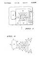
- FIG. 7illustrates, in block diagram form, an integrated circuit inspection system of the present invention.
- FIG. 1illustrates a highly magnified view of a portion of an integrated circuit 11.
- a relatively simple bipolar integrated circuitis shown for ease of description, it should be understood that the method of the present invention is equally applicable to very complex integrated circuits having thousands or millions of components and is applicable to CMOS, bipolar, or any similar integrated circuit manufacturing technology.
- Integrated circuit 11comprises an isolation region 18 in which is formed a collector region 17.
- Base region 16is formed in collector region 17 and emitter region (not shown) is formed near the central portion of base region 16 under emitter electrode 14.
- Base region 16is contacted by base fingers 13 which are coupled to bonding pad 12.
- Bonding pad 12, base fingers 13, and emitter interconnect 14are formed of metal, while base 16, collector 17, and isolation region 18 are covered by oxides of various thicknesses. Because oxide over various portions of integrated circuit 11 have different thicknesses, each region appears to have a different color when exposed to white light.
- the emitter, base, collector, and isolation regions, as well as device regionsare easily discernible under white light, although occasionally it may be necessary to filter the light to increase definition between regions.
- a difficulty with conventional inspection systemsis that the actual color of each of the regions may vary significantly from wafer to wafer or even from device to device on a single wafer. While each of the regions remains easily discernible to the naked eye, this change in absolute color often confuses an image processing system. This confusion leads to judgment errors in identifying good and bad device structures and leads to an increased amount of operator intervention to fine tune optics or manually inspect portions of a wafer.
- a particular advantage of the present inventionis its ability to accurately inspect the surface of an integrated circuit with even widely varying colors across a single wafer. It is this aspect of the present invention which is referred to as "robustness".
- FIG. 2illustrates a direction edge enhanced image of bonding pad 12, base fingers 13, and emitter electrode 14.
- FIG. 2shows the metallization pattern which is shown in FIG. 1 including bonding pad 12, base fingers 13, and emitter interconnect 14.
- Base 16, collector 17, and isolation region 18have been omitted from FIG. 2 for ease of illustration, but it should be understood that the alignment and quality of these regions can be inspected simultaneously with the metallization pattern shown in FIG. 2. It should also be understood that by varying light conditions and/or intelligently varying the threshold conditions of the image analysis system, that specific areas or layers of integrated circuit 11 can be analyzed while ignoring other layers. This feature will become more apparent during the discussion of defect classification which follows.
- a direction edge enhanced imageidentifies edges of interest in the pattern shown in FIG. 1 using any of a number of well known image analysis algorithms.
- the direction edge enhanced imageincludes east edges 21, West edges 22, South edges 23, and North edges 24.
- the direction edgescombine to form a direction edge shape which is merely a shape contained by a series of connecting direction edges.
- Direction edge enhancementaffords many advantages in image processing including reduced quantity of data, greater flexibility of data, and immunity to such variations as illumination intensity and color variation in the image.
- the direction edge enhanced imagecontains all information of interest in inspection while using a fraction of the data which would be required using a pure gray scale analysis technology.
- the method of the present inventioncompares direction edge images of two similar integrated circuits to identify anomalies or defects in one of the integrated circuits.
- the two integrated circuitsmay be adjacent to each other or located in different areas of the wafer, or indeed located on entirely different wafers. It is useful, however, if the integrated circuits are adjacent to each other as this greatly eases compensation for color variation and pattern magnification which occurs during normal semiconductor processing.
- first image, or sample imageis obtained and analyzed.
- the analysisincludes a direction edge enhancement of the sample image as shown in FIG. 2, and preferably includes a morphological dilation, as shown in FIG. 3.
- Morphological dilation of the direction edge shapeis nothing more than a mathematical transformation of the direction edge shape which has the effect of growing the direction edge shape's boundary by one or more picture elements or pixels. This results in a swelled, or dilated direction edge image illustrated by dashed line 26 in FIG. 3. Dilated direction edge shapes of the sample integrated circuit are stored for future comparison.
- FIG. 4illustrates a direction edge shape of an integrated circuit under inspection which will be compared to the dilated direction edge shape 26 shown in FIG. 3.
- the direction edges in FIG. 4 and FIG. 3are not individually labeled as they were in FIG. 2 but it should be understood both FIG. 4 and FIG. 3 illustrate in solid lines the same direction edge enhanced image shown in FIG. 2.
- the direction edge shape of the integrated circuit under inspectionis skeletonized or eroded to produce a skeletonized direction edge shape illustrated by dashed lines 27.
- the skeletonizd processis another mathematical transformation opposite the dilation process in that direction edge shapes are shrunk by one or more picture elements.
- Mask flaw 28 and debris 29also produce direction edge shapes which are skeletonized.
- the skeletonization processreduces the overall size of the direction edge shape while maintaining critical information such as overall shape and position.
- the dilation process illustrated in FIG. 3 and the skeletonization process shown in FIG. 4are optional but greatly improve the robustness of the image analysis system.
- Skeletonized shape 27is subsequently compared to dilated shape 26 as shown in FIG. 5A.
- This comparisonis performed by logically comparing points which make up skeletonized image 27 to determine if they fit within the boundaries defined by dilated image 26. Those points which do not fit within the boundaries of dilated image 26 indicate anomalies or defects in the pattern. The location for each anomaly or defect is determined and recorded. Additionally, further information such as size and shape of each defect can be recorded. Further analysis and classification of defects 29 and 28 will be described hereinafter in reference to FIG. 6.
- the logical comparison stepcan be performed by a system computer which is coupled to image analysis computer.
- FIG. 5Billustrates the advantage of the dilation and skeletonization processes.
- skeletonized image 27is rotted somewhat with respect to dilated image 26.
- Acceptable image variationsinclude rotation, as shown in FIG. 5B, as well as absolute location variation, also called x or y shift, and magnification variation.
- Such image variationscan easily occur in a manufacturing environment due to either misregistration of a wafer under inspection or shifting of the optics which make up the inspection system. It can be seen however that skeletonized image 27 still remains within the boundaries of dilated image 26 except for flaw 28 and defect 29. Thus, even when normal errors occur in the inspection equipment a correct analysis of the integrated circuit is provided.
- analysis of the sample integrated circuit and analysis of the integrated circuit under inspectioncan be performed sequentially or in parallel depending on the equipment setup.
- parallel inspectionwould require two sets of optics to view the sample integrated circuit and the integrated circuit under inspection simultaneously.
- the direction edge image or dilated direction edge image 26 shown in FIG. 2must be stored while the image of the integrated circuit under inspection is analyzed. Since the logical comparison between the two images is performed digitally by a computer either parallel inspection or sequential inspection and comparison are acceptable applications of the present invention. Particular choice of operation will be decided by capital expenditure and operating speed demands.
- defects 29 and 28are identified it is very useful to automatically classify these defects. This classification provides useful information for process control and reliability prediction.
- Basic informationsuch as defect location, size, and shape can be obtained directly by mathematical analysis of the direction edge shape which has been identified as a defect. More detailed analysis can be provided by obtaining a plurality of images of each defect under a variety of lighting conditions. For example, each defect can be illuminated with red, blue, and green light and/or can be illuminated with light at varying angles of incidence.
- FIG. 6A and 6Billustrate a defect which is illuminated under two different light conditions. Both FIG. 6A and 6B show a highly magnified portion of integrated circuit 11 with a defect 31 which occurs over an active region 32.
- FIGS. 6A and 6Bshow direction edge images obtained by the image analysis system under differing light conditions. Background region 33 may be another active device region or an inactive portion of integrated circuit 11.
- Direction edges, which are derived from the image,are shown in solid lines, while dashed lines indicate portions of the actual image which are not represented by direction edges under a particular lighting condition.
- Direction edges of an imageare identified by locating portions of the image where reflected light intensity changes. If two portions of the image reflect nearly the same light intensity, edge information is difficult to discern as the two portions of the image appear to be one continuous portion. Usually, direction edge analysis is performed under broad spectrum lighting to maximize the difference in reflected light intensity.
- the present inventionuses predetermined lighting conditions to selectively enhance and diminish edge features.
- FIG. 6Bshows the same integrated circuit under a different lighting condition in which the difference between active area 32 and background 33 is not discernable, but defect 31 is discernable.
- the set of direction edge data shown by solid lines in FIG. 6Bforms a second feature vector describing the defect and surrounding integrated circuit. It should be noted that the direction edge information contained in each of the feature vectors is unique to the lighting condition.
- any number of lighting angles and lighting colorscan be used to provide additional feature vectors although lighting with the primary colors red, green, and blue combined with just a few incident light angles is believed to provide enough information to correctly classify most defects.
- the plurality of feature vectorsare combined to form a feature matrix describing the defect.
- This feature matrixis then fed into an expert system database which compiles information on feature matrices and associates feature matrices with defect classifications. As this database builds up it can be used to classify defects without assistance from an expert.
- FIG. 7A block diagram of the expert system defect classification of the present invention is shown in FIG. 7.
- Integrated circuits 11are illuminated by a variety of light sources 34 which are described hereinbefore.
- An industrial television camera 38detects the image from integrated circuits 11 and feeds the image information to a high speed image computer 35.
- High speed image computer 35is particularly adapted for processing both binary and gray level images and performing such functions as direction edge enhancement, morphological dilation, and morphological skeletonization. This processed image is then sent to a monitor on which an operator can visually observe the inspection process.
- High speed image computer 35is also coupled to a system computer 37 which performs such functions as determining a location size and shape of various features and defects on integrated circuit 11.
- System computer 37also compiles feature vectors and build feature matrices during defect classification process. Feature matrices are then fed to expert system 38 which classified the defects and stores the feature matrices with the defect classification for future reference.
- defect locationscan be easily identified and stored on a real time basis for all of the integrated circuits on a wafer. Further, defects which are located can be analyzed using a variety of lighting sources to obtain a plurality of defect images which are converted to feature vectors. Feature vectors are combined to build feature matrices which are then unique identifiers which can be used to classify the defects providing valuable information for process control and circuit reliability.
Landscapes
- Engineering & Computer Science (AREA)
- General Physics & Mathematics (AREA)
- Physics & Mathematics (AREA)
- Immunology (AREA)
- Analytical Chemistry (AREA)
- Biochemistry (AREA)
- General Health & Medical Sciences (AREA)
- Chemical & Material Sciences (AREA)
- Life Sciences & Earth Sciences (AREA)
- Pathology (AREA)
- Health & Medical Sciences (AREA)
- Quality & Reliability (AREA)
- Computer Vision & Pattern Recognition (AREA)
- Theoretical Computer Science (AREA)
- Testing Or Measuring Of Semiconductors Or The Like (AREA)
- Investigating Materials By The Use Of Optical Means Adapted For Particular Applications (AREA)
Abstract
Description
Claims (3)
Priority Applications (1)
| Application Number | Priority Date | Filing Date | Title |
|---|---|---|---|
| US07/533,207US5129009A (en) | 1990-06-04 | 1990-06-04 | Method for automatic semiconductor wafer inspection |
Applications Claiming Priority (1)
| Application Number | Priority Date | Filing Date | Title |
|---|---|---|---|
| US07/533,207US5129009A (en) | 1990-06-04 | 1990-06-04 | Method for automatic semiconductor wafer inspection |
Publications (1)
| Publication Number | Publication Date |
|---|---|
| US5129009Atrue US5129009A (en) | 1992-07-07 |
Family
ID=24124959
Family Applications (1)
| Application Number | Title | Priority Date | Filing Date |
|---|---|---|---|
| US07/533,207Expired - LifetimeUS5129009A (en) | 1990-06-04 | 1990-06-04 | Method for automatic semiconductor wafer inspection |
Country Status (1)
| Country | Link |
|---|---|
| US (1) | US5129009A (en) |
Cited By (59)
| Publication number | Priority date | Publication date | Assignee | Title |
|---|---|---|---|---|
| US5237621A (en)* | 1991-08-08 | 1993-08-17 | Philip Morris Incorporated | Product appearance inspection methods and apparatus employing low variance filter |
| US5237404A (en)* | 1990-06-28 | 1993-08-17 | Mazda Motor Corporation | Inspection apparatus with improved detection of surface defects over large and curved surfaces |
| US5293324A (en)* | 1991-04-15 | 1994-03-08 | Matsushita Electric Industrial Co., Ltd. | Method and apparatus for inspecting solder portions using fuzzy inference |
| US5351307A (en)* | 1991-11-15 | 1994-09-27 | Societe Nationale D'etude Et De Construction De Moteurs D'aviation "S.N.E.C.M.A." | Process and apparatus for the acquisition and processing of screen images |
| US5365596A (en)* | 1992-12-17 | 1994-11-15 | Philip Morris Incorporated | Methods and apparatus for automatic image inspection of continuously moving objects |
| US5452368A (en)* | 1993-08-02 | 1995-09-19 | Motorola, Inc. | Method of detecting defects in semiconductor package leads |
| US5544256A (en)* | 1993-10-22 | 1996-08-06 | International Business Machines Corporation | Automated defect classification system |
| US5600734A (en)* | 1991-10-04 | 1997-02-04 | Fujitsu Limited | Electron beam tester |
| US5649169A (en)* | 1995-06-20 | 1997-07-15 | Advanced Micro Devices, Inc. | Method and system for declustering semiconductor defect data |
| US5682440A (en)* | 1992-09-07 | 1997-10-28 | Matsushita Electric Industrial Co., Ltd. | Method of extracting pixels constituting intensity changes in an image and method of identifying collection of intensity changes |
| WO1998006874A1 (en)* | 1995-08-09 | 1998-02-19 | The Regents Of The University Of California | Systems for generating and analyzing stimulus-response output signal matrices |
| US5801764A (en)* | 1994-07-11 | 1998-09-01 | Tokyo Electron Limited | Monitor device and monitor method |
| US5801965A (en)* | 1993-12-28 | 1998-09-01 | Hitachi, Ltd. | Method and system for manufacturing semiconductor devices, and method and system for inspecting semiconductor devices |
| US5859698A (en)* | 1997-05-07 | 1999-01-12 | Nikon Corporation | Method and apparatus for macro defect detection using scattered light |
| US5978501A (en)* | 1997-01-03 | 1999-11-02 | International Business Machines Corporation | Adaptive inspection method and system |
| US5982920A (en)* | 1997-01-08 | 1999-11-09 | Lockheed Martin Energy Research Corp. Oak Ridge National Laboratory | Automated defect spatial signature analysis for semiconductor manufacturing process |
| AU720427B2 (en)* | 1996-08-12 | 2000-06-01 | Regents Of The University Of California, The | Systems for generating and analyzing stimulus-response output signal matrices |
| US6097428A (en)* | 1997-05-23 | 2000-08-01 | Inspex, Inc. | Method and apparatus for inspecting a semiconductor wafer using a dynamic threshold |
| WO2000055636A1 (en)* | 1999-03-16 | 2000-09-21 | Proteome Systems Ltd. | Method and apparatus for manipulating arrays |
| US6177287B1 (en)* | 1998-09-28 | 2001-01-23 | Advanced Micro Devices, Inc. | Simplified inter database communication system |
| US6304680B1 (en) | 1997-10-27 | 2001-10-16 | Assembly Guidance Systems, Inc. | High resolution, high accuracy process monitoring system |
| US6326140B1 (en) | 1995-08-09 | 2001-12-04 | Regents Of The University Of California | Systems for generating and analyzing stimulus-response output signal matrices |
| US6418353B1 (en)* | 1998-04-22 | 2002-07-09 | Lsi Logic Corporation | Automating photolithography in the fabrication of integrated circuits |
| US6444992B1 (en) | 1998-09-30 | 2002-09-03 | Trellis Bioscience, Inc. | High throughput microscopy |
| US6535776B1 (en) | 1999-09-20 | 2003-03-18 | Ut-Battelle, Llc | Method for localizing and isolating an errant process step |
| US6546308B2 (en) | 1993-12-28 | 2003-04-08 | Hitachi, Ltd, | Method and system for manufacturing semiconductor devices, and method and system for inspecting semiconductor devices |
| US20030072481A1 (en)* | 2001-10-11 | 2003-04-17 | Advanced Micro Devices, Inc. | Method for evaluating anomalies in a semiconductor manufacturing process |
| WO2003044741A1 (en)* | 2001-11-16 | 2003-05-30 | Proteome Systems Intellectual Property Pty Ltd | Method for locating the edge of an object |
| US20030175321A1 (en)* | 1999-01-26 | 2003-09-18 | Sapieszko Ronald S. | Inorganic shaped bodies and methods for their production and use |
| WO2003081531A1 (en)* | 2002-03-21 | 2003-10-02 | Camtek Ltd. | A morphological inspection method based on skeletonization |
| AU766920B2 (en)* | 2001-01-30 | 2003-10-23 | Randox Laboratories Ltd. | Imaging method |
| US6667800B1 (en)* | 1997-02-17 | 2003-12-23 | Volvo Car Corporation | Method and device for measuring and quantifying surface defects on a test surface |
| US20040047140A1 (en)* | 1999-04-27 | 2004-03-11 | Kurt Pelsue | Programmable illuminator for vision system |
| US20040165762A1 (en)* | 2003-02-25 | 2004-08-26 | Lamda-Lite Enterprises, Inc. | System and method for detecting and reporting fabrication defects using a multi-variant image analysis |
| US20040179726A1 (en)* | 1996-08-14 | 2004-09-16 | James Burdorf | Process for detecting defects in photomasks |
| US6868175B1 (en)* | 1999-08-26 | 2005-03-15 | Nanogeometry Research | Pattern inspection apparatus, pattern inspection method, and recording medium |
| US20050146714A1 (en)* | 1999-08-26 | 2005-07-07 | Tadashi Kitamura | Pattern inspection apparatus and method |
| USRE38900E1 (en) | 1995-08-08 | 2005-11-29 | Lsi Logic Corporation | Automating photolithography in the fabrication of integrated circuits |
| US20060067570A1 (en)* | 2004-09-29 | 2006-03-30 | Dainippon Screen Mfg. Co., Ltd. | Apparatus and method for inspecting pattern |
| US20060072850A1 (en)* | 2002-01-04 | 2006-04-06 | America Online, Inc. A Delaware Corporation | Registration of separations |
| US20060245636A1 (en)* | 1999-08-26 | 2006-11-02 | Tadashi Kitamura | Pattern inspection apparatus and method |
| US20080130982A1 (en)* | 2006-12-05 | 2008-06-05 | Tadashi Kitamura | Pattern inspection apparatus and method |
| US20080240544A1 (en)* | 2003-03-14 | 2008-10-02 | Kabushiki Kaisha Toshiba | System for creating an inspection recipe, system for reviewing defects, method for creating an inspection recipe and method for reviewing defects |
| US7558419B1 (en)* | 2003-08-14 | 2009-07-07 | Brion Technologies, Inc. | System and method for detecting integrated circuit pattern defects |
| US20090239315A1 (en)* | 2008-03-24 | 2009-09-24 | Promos Technologies Inc. | Method and system for processing test wafer in photolithography process |
| WO2010049924A1 (en)* | 2008-10-28 | 2010-05-06 | Orbotech Ltd. | Producing electrical circuit patterns using multi-population transformation |
| US20100158393A1 (en)* | 2008-12-19 | 2010-06-24 | Hong Fu Jin Precision Industry (Shenzhen) Co., Ltd. | Image comparison system and method |
| CN103018265A (en)* | 2012-11-28 | 2013-04-03 | 上海华力微电子有限公司 | Method for positioning defect of semiconductor |
| US20140168419A1 (en)* | 2011-07-13 | 2014-06-19 | Koh Young Technology Inc. | Inspection method |
| US9241128B2 (en) | 2013-02-14 | 2016-01-19 | Warner Bros. Entertainment Inc. | Video conversion technology |
| US9265458B2 (en) | 2012-12-04 | 2016-02-23 | Sync-Think, Inc. | Application of smooth pursuit cognitive testing paradigms to clinical drug development |
| US9380976B2 (en) | 2013-03-11 | 2016-07-05 | Sync-Think, Inc. | Optical neuroinformatics |
| US20160275670A1 (en)* | 2015-03-17 | 2016-09-22 | MTU Aero Engines AG | Method and device for the quality evaluation of a component produced by means of an additive manufacturing method |
| US9612273B2 (en) | 2014-11-28 | 2017-04-04 | Exnodes Inc. | Distributed wafer inspection |
| US20170160338A1 (en)* | 2015-12-07 | 2017-06-08 | Intel Corporation | Integrated circuit reliability assessment apparatus and method |
| WO2018134286A1 (en)* | 2017-01-18 | 2018-07-26 | Asml Netherlands B.V. | Defect pattern grouping method and system |
| CN108665439A (en)* | 2017-08-22 | 2018-10-16 | 深圳安博电子有限公司 | Method of testing substrate and terminal device |
| WO2025038524A1 (en)* | 2023-08-16 | 2025-02-20 | Applied Materials, Inc. | Large format continuous imaging system |
| WO2025049065A1 (en)* | 2023-09-01 | 2025-03-06 | Applied Materials, Inc. | Multidirectional illumination for hybrid bonding defect detection |
Citations (11)
| Publication number | Priority date | Publication date | Assignee | Title |
|---|---|---|---|---|
| US4441207A (en)* | 1982-01-19 | 1984-04-03 | Environmental Research Institute Of Michigan | Design rule checking using serial neighborhood processors |
| US4477926A (en)* | 1980-12-18 | 1984-10-16 | International Business Machines Corporation | Process for inspecting and automatically sorting objects showing patterns with constant dimensional tolerances and apparatus for carrying out said process |
| US4481664A (en)* | 1980-12-18 | 1984-11-06 | International Business Machines Corporation | Process for inspecting objects showing patterns with dimensional tolerances and reject criteria varying with the locations of said patterns and apparatus and circuits for carrying out said process |
| US4618938A (en)* | 1984-02-22 | 1986-10-21 | Kla Instruments Corporation | Method and apparatus for automatic wafer inspection |
| US4648052A (en)* | 1983-11-14 | 1987-03-03 | Sentient Systems Technology, Inc. | Eye-tracker communication system |
| US4659220A (en)* | 1984-10-22 | 1987-04-21 | International Business Machines Corporation | Optical inspection system for semiconductor wafers |
| US4731855A (en)* | 1984-04-06 | 1988-03-15 | Hitachi, Ltd. | Pattern defect inspection apparatus |
| US4805123A (en)* | 1986-07-14 | 1989-02-14 | Kla Instruments Corporation | Automatic photomask and reticle inspection method and apparatus including improved defect detector and alignment sub-systems |
| US4853967A (en)* | 1984-06-29 | 1989-08-01 | International Business Machines Corporation | Method for automatic optical inspection analysis of integrated circuits |
| US4893346A (en)* | 1985-03-14 | 1990-01-09 | Beltronics, Inc. | Apparatus for automatically inspecting objects and identifying or recognizing known and unknown portions thereof, including defects and the like, and method |
| US4965842A (en)* | 1986-07-22 | 1990-10-23 | Schlumberger Technologies, Inc. | Method and apparatus for measuring feature dimensions using controlled dark-field illumination |
- 1990
- 1990-06-04USUS07/533,207patent/US5129009A/ennot_activeExpired - Lifetime
Patent Citations (12)
| Publication number | Priority date | Publication date | Assignee | Title |
|---|---|---|---|---|
| US4477926A (en)* | 1980-12-18 | 1984-10-16 | International Business Machines Corporation | Process for inspecting and automatically sorting objects showing patterns with constant dimensional tolerances and apparatus for carrying out said process |
| US4481664A (en)* | 1980-12-18 | 1984-11-06 | International Business Machines Corporation | Process for inspecting objects showing patterns with dimensional tolerances and reject criteria varying with the locations of said patterns and apparatus and circuits for carrying out said process |
| US4441207A (en)* | 1982-01-19 | 1984-04-03 | Environmental Research Institute Of Michigan | Design rule checking using serial neighborhood processors |
| US4648052A (en)* | 1983-11-14 | 1987-03-03 | Sentient Systems Technology, Inc. | Eye-tracker communication system |
| US4618938A (en)* | 1984-02-22 | 1986-10-21 | Kla Instruments Corporation | Method and apparatus for automatic wafer inspection |
| US4731855A (en)* | 1984-04-06 | 1988-03-15 | Hitachi, Ltd. | Pattern defect inspection apparatus |
| US4853967A (en)* | 1984-06-29 | 1989-08-01 | International Business Machines Corporation | Method for automatic optical inspection analysis of integrated circuits |
| US4659220A (en)* | 1984-10-22 | 1987-04-21 | International Business Machines Corporation | Optical inspection system for semiconductor wafers |
| US4893346A (en)* | 1985-03-14 | 1990-01-09 | Beltronics, Inc. | Apparatus for automatically inspecting objects and identifying or recognizing known and unknown portions thereof, including defects and the like, and method |
| US4805123A (en)* | 1986-07-14 | 1989-02-14 | Kla Instruments Corporation | Automatic photomask and reticle inspection method and apparatus including improved defect detector and alignment sub-systems |
| US4805123B1 (en)* | 1986-07-14 | 1998-10-13 | Kla Instr Corp | Automatic photomask and reticle inspection method and apparatus including improved defect detector and alignment sub-systems |
| US4965842A (en)* | 1986-07-22 | 1990-10-23 | Schlumberger Technologies, Inc. | Method and apparatus for measuring feature dimensions using controlled dark-field illumination |
Cited By (107)
| Publication number | Priority date | Publication date | Assignee | Title |
|---|---|---|---|---|
| US5825912A (en)* | 1901-12-16 | 1998-10-20 | Fujitsu Limited | Electron beam tester |
| US5237404A (en)* | 1990-06-28 | 1993-08-17 | Mazda Motor Corporation | Inspection apparatus with improved detection of surface defects over large and curved surfaces |
| US5293324A (en)* | 1991-04-15 | 1994-03-08 | Matsushita Electric Industrial Co., Ltd. | Method and apparatus for inspecting solder portions using fuzzy inference |
| US5537670A (en)* | 1991-08-08 | 1996-07-16 | Philip Morris Incorporated | Product appearance inspection methods and apparatus employing low variance filter |
| US5237621A (en)* | 1991-08-08 | 1993-08-17 | Philip Morris Incorporated | Product appearance inspection methods and apparatus employing low variance filter |
| US5600734A (en)* | 1991-10-04 | 1997-02-04 | Fujitsu Limited | Electron beam tester |
| US5872862A (en)* | 1991-10-04 | 1999-02-16 | Fujitsu Limited | Electron beam tester |
| US5351307A (en)* | 1991-11-15 | 1994-09-27 | Societe Nationale D'etude Et De Construction De Moteurs D'aviation "S.N.E.C.M.A." | Process and apparatus for the acquisition and processing of screen images |
| US5682440A (en)* | 1992-09-07 | 1997-10-28 | Matsushita Electric Industrial Co., Ltd. | Method of extracting pixels constituting intensity changes in an image and method of identifying collection of intensity changes |
| US5365596A (en)* | 1992-12-17 | 1994-11-15 | Philip Morris Incorporated | Methods and apparatus for automatic image inspection of continuously moving objects |
| US5452368A (en)* | 1993-08-02 | 1995-09-19 | Motorola, Inc. | Method of detecting defects in semiconductor package leads |
| US5544256A (en)* | 1993-10-22 | 1996-08-06 | International Business Machines Corporation | Automated defect classification system |
| US6546308B2 (en) | 1993-12-28 | 2003-04-08 | Hitachi, Ltd, | Method and system for manufacturing semiconductor devices, and method and system for inspecting semiconductor devices |
| US6438438B1 (en) | 1993-12-28 | 2002-08-20 | Hitachi, Ltd. | Method and system for manufacturing semiconductor devices, and method and system for inspecting semiconductor devices |
| US5801965A (en)* | 1993-12-28 | 1998-09-01 | Hitachi, Ltd. | Method and system for manufacturing semiconductor devices, and method and system for inspecting semiconductor devices |
| US5801764A (en)* | 1994-07-11 | 1998-09-01 | Tokyo Electron Limited | Monitor device and monitor method |
| US5831865A (en)* | 1995-06-20 | 1998-11-03 | Advanced Micro Devices, Inc. | Method and system for declusturing semiconductor defect data |
| US5649169A (en)* | 1995-06-20 | 1997-07-15 | Advanced Micro Devices, Inc. | Method and system for declustering semiconductor defect data |
| USRE38900E1 (en) | 1995-08-08 | 2005-11-29 | Lsi Logic Corporation | Automating photolithography in the fabrication of integrated circuits |
| US6574568B2 (en) | 1995-08-09 | 2003-06-03 | Regents Of The University Of California | Systems for generating and analyzing stimulus-response output signal matrices |
| WO1998006874A1 (en)* | 1995-08-09 | 1998-02-19 | The Regents Of The University Of California | Systems for generating and analyzing stimulus-response output signal matrices |
| US20020064797A1 (en)* | 1995-08-09 | 2002-05-30 | Regents Of The University Of California | Systems for generating and analyzing stimulus-response output signal matrices |
| US6326140B1 (en) | 1995-08-09 | 2001-12-04 | Regents Of The University Of California | Systems for generating and analyzing stimulus-response output signal matrices |
| US5777888A (en)* | 1995-08-09 | 1998-07-07 | Regents Of The University Of California | Systems for generating and analyzing stimulus-response output signal matrices |
| AU720427B2 (en)* | 1996-08-12 | 2000-06-01 | Regents Of The University Of California, The | Systems for generating and analyzing stimulus-response output signal matrices |
| US20040179726A1 (en)* | 1996-08-14 | 2004-09-16 | James Burdorf | Process for detecting defects in photomasks |
| US5978501A (en)* | 1997-01-03 | 1999-11-02 | International Business Machines Corporation | Adaptive inspection method and system |
| US5982920A (en)* | 1997-01-08 | 1999-11-09 | Lockheed Martin Energy Research Corp. Oak Ridge National Laboratory | Automated defect spatial signature analysis for semiconductor manufacturing process |
| US6667800B1 (en)* | 1997-02-17 | 2003-12-23 | Volvo Car Corporation | Method and device for measuring and quantifying surface defects on a test surface |
| US5859698A (en)* | 1997-05-07 | 1999-01-12 | Nikon Corporation | Method and apparatus for macro defect detection using scattered light |
| US6097428A (en)* | 1997-05-23 | 2000-08-01 | Inspex, Inc. | Method and apparatus for inspecting a semiconductor wafer using a dynamic threshold |
| US6304680B1 (en) | 1997-10-27 | 2001-10-16 | Assembly Guidance Systems, Inc. | High resolution, high accuracy process monitoring system |
| US6418353B1 (en)* | 1998-04-22 | 2002-07-09 | Lsi Logic Corporation | Automating photolithography in the fabrication of integrated circuits |
| US6177287B1 (en)* | 1998-09-28 | 2001-01-23 | Advanced Micro Devices, Inc. | Simplified inter database communication system |
| US6444992B1 (en) | 1998-09-30 | 2002-09-03 | Trellis Bioscience, Inc. | High throughput microscopy |
| US20030175321A1 (en)* | 1999-01-26 | 2003-09-18 | Sapieszko Ronald S. | Inorganic shaped bodies and methods for their production and use |
| WO2000055636A1 (en)* | 1999-03-16 | 2000-09-21 | Proteome Systems Ltd. | Method and apparatus for manipulating arrays |
| US20040047140A1 (en)* | 1999-04-27 | 2004-03-11 | Kurt Pelsue | Programmable illuminator for vision system |
| US20050226494A1 (en)* | 1999-08-26 | 2005-10-13 | Nanogeometry Research | Pattern inspection apparatus, pattern inspection method, and recording medium |
| US7796801B2 (en) | 1999-08-26 | 2010-09-14 | Nanogeometry Research Inc. | Pattern inspection apparatus and method |
| US7817844B2 (en) | 1999-08-26 | 2010-10-19 | Nanogeometry Research Inc. | Pattern inspection apparatus and method |
| US6868175B1 (en)* | 1999-08-26 | 2005-03-15 | Nanogeometry Research | Pattern inspection apparatus, pattern inspection method, and recording medium |
| US20050146714A1 (en)* | 1999-08-26 | 2005-07-07 | Tadashi Kitamura | Pattern inspection apparatus and method |
| US20060245636A1 (en)* | 1999-08-26 | 2006-11-02 | Tadashi Kitamura | Pattern inspection apparatus and method |
| US7660455B2 (en) | 1999-08-26 | 2010-02-09 | Nanogeometry Research Inc. | Pattern inspection apparatus, pattern inspection method, and recording medium |
| US6535776B1 (en) | 1999-09-20 | 2003-03-18 | Ut-Battelle, Llc | Method for localizing and isolating an errant process step |
| AU766920B2 (en)* | 2001-01-30 | 2003-10-23 | Randox Laboratories Ltd. | Imaging method |
| US20030072481A1 (en)* | 2001-10-11 | 2003-04-17 | Advanced Micro Devices, Inc. | Method for evaluating anomalies in a semiconductor manufacturing process |
| US20050053268A1 (en)* | 2001-11-16 | 2005-03-10 | Breen Edmond Joseph | Method for locating the edge of an object |
| WO2003044741A1 (en)* | 2001-11-16 | 2003-05-30 | Proteome Systems Intellectual Property Pty Ltd | Method for locating the edge of an object |
| US7272268B2 (en)* | 2002-01-04 | 2007-09-18 | Aol Llc | Registration of separations |
| US8818088B2 (en) | 2002-01-04 | 2014-08-26 | Warner Bros. Entertainment Inc. | Registration of separations |
| US20060072850A1 (en)* | 2002-01-04 | 2006-04-06 | America Online, Inc. A Delaware Corporation | Registration of separations |
| US20080056614A1 (en)* | 2002-01-04 | 2008-03-06 | Warner Bros. Entertainment Inc. | Registration of separations |
| US9104938B2 (en) | 2002-01-04 | 2015-08-11 | Warner Bros. Entertainment Inc. | Registration of separations |
| US20080137979A1 (en)* | 2002-01-04 | 2008-06-12 | Warner Bros. Entertainment Inc. | Registration of separations |
| US9773314B2 (en) | 2002-01-04 | 2017-09-26 | Warner Bros. Entertainment Inc. | Registration of separations |
| US20100150469A1 (en)* | 2002-01-04 | 2010-06-17 | Warner Bros. Entertainment Inc. | Registration of Separations |
| US7486842B2 (en) | 2002-01-04 | 2009-02-03 | Warner Bros. Entertainment Inc. | Registration of separations |
| US8094972B2 (en) | 2002-01-04 | 2012-01-10 | Warner Bros. Entertainment Inc. | Registration of separations |
| US7672541B2 (en) | 2002-01-04 | 2010-03-02 | Warner Bros. Entertainment Inc. | Registration of separations |
| US8401337B2 (en) | 2002-01-04 | 2013-03-19 | Warner Bros. Entertainment Inc. | Registration of separations |
| US20060233433A1 (en)* | 2002-03-21 | 2006-10-19 | Roni Flieswasser | Morphological inspection method based on skeletonization |
| US7570799B2 (en) | 2002-03-21 | 2009-08-04 | Camtek Ltd. | Morphological inspection method based on skeletonization |
| WO2003081531A1 (en)* | 2002-03-21 | 2003-10-02 | Camtek Ltd. | A morphological inspection method based on skeletonization |
| US20040165762A1 (en)* | 2003-02-25 | 2004-08-26 | Lamda-Lite Enterprises, Inc. | System and method for detecting and reporting fabrication defects using a multi-variant image analysis |
| US7463765B2 (en) | 2003-02-25 | 2008-12-09 | Lamda-Lite Enterprises Incorporated | System and method for detecting and reporting fabrication defects using a multi-variant image analysis |
| US20110001820A1 (en)* | 2003-03-14 | 2011-01-06 | Kabushiki Kaisha Toshiba | System for creating an inspection recipe, system for reviewing defects, method for creating an inspection recipe and method for reviewing defects |
| US20080240544A1 (en)* | 2003-03-14 | 2008-10-02 | Kabushiki Kaisha Toshiba | System for creating an inspection recipe, system for reviewing defects, method for creating an inspection recipe and method for reviewing defects |
| US7558419B1 (en)* | 2003-08-14 | 2009-07-07 | Brion Technologies, Inc. | System and method for detecting integrated circuit pattern defects |
| US7689029B2 (en)* | 2004-09-29 | 2010-03-30 | Dainippon Screen Mfg. Co., Ltd. | Apparatus and method for inspecting pattern |
| US20060067570A1 (en)* | 2004-09-29 | 2006-03-30 | Dainippon Screen Mfg. Co., Ltd. | Apparatus and method for inspecting pattern |
| US20100150426A1 (en)* | 2004-09-29 | 2010-06-17 | Dainippon Screen Mfg. Co., Ltd. | Apparatus and method for inspecting pattern |
| US9189843B2 (en) | 2006-12-05 | 2015-11-17 | Ngr Inc. | Pattern inspection apparatus and method |
| US20110235895A1 (en)* | 2006-12-05 | 2011-09-29 | Ngr Inc. | Pattern inspection apparatus and method |
| US7983471B2 (en) | 2006-12-05 | 2011-07-19 | Ngr Inc. | Pattern inspection apparatus and method |
| US8285031B2 (en) | 2006-12-05 | 2012-10-09 | Ngr Inc. | Pattern inspection apparatus and method |
| US20080130982A1 (en)* | 2006-12-05 | 2008-06-05 | Tadashi Kitamura | Pattern inspection apparatus and method |
| US20090239315A1 (en)* | 2008-03-24 | 2009-09-24 | Promos Technologies Inc. | Method and system for processing test wafer in photolithography process |
| US20110155424A1 (en)* | 2008-10-28 | 2011-06-30 | Orbotech Ltd. | Producing electrical circuit patterns using multi-population transformation |
| WO2010049924A1 (en)* | 2008-10-28 | 2010-05-06 | Orbotech Ltd. | Producing electrical circuit patterns using multi-population transformation |
| CN102197397B (en)* | 2008-10-28 | 2015-05-06 | 奥博泰克有限公司 | Producing electrical circuit patterns using multi-population transformation |
| US8769471B2 (en) | 2008-10-28 | 2014-07-01 | Orbotech Ltd. | Producing electrical circuit patterns using multi-population transformation |
| CN101751575B (en)* | 2008-12-19 | 2012-12-19 | 鸿富锦精密工业(深圳)有限公司 | Image comparison system and method |
| US8249363B2 (en)* | 2008-12-19 | 2012-08-21 | Hong Fu Jin Precision Industry (Shenzhen) Co., Ltd. | Image comparison system and method |
| US20100158393A1 (en)* | 2008-12-19 | 2010-06-24 | Hong Fu Jin Precision Industry (Shenzhen) Co., Ltd. | Image comparison system and method |
| US20140168419A1 (en)* | 2011-07-13 | 2014-06-19 | Koh Young Technology Inc. | Inspection method |
| US10706521B2 (en)* | 2011-07-13 | 2020-07-07 | Koh Young Technology Inc. | Inspection method |
| CN103018265B (en)* | 2012-11-28 | 2015-05-20 | 上海华力微电子有限公司 | Method for positioning defect of semiconductor |
| CN103018265A (en)* | 2012-11-28 | 2013-04-03 | 上海华力微电子有限公司 | Method for positioning defect of semiconductor |
| US9265458B2 (en) | 2012-12-04 | 2016-02-23 | Sync-Think, Inc. | Application of smooth pursuit cognitive testing paradigms to clinical drug development |
| US9723257B2 (en) | 2013-02-14 | 2017-08-01 | Warner Bros. Entertainment Inc. | Video conversion technology |
| US10277862B2 (en) | 2013-02-14 | 2019-04-30 | Warner Bros. Entertainment Inc. | Video conversion technology |
| US11997417B2 (en) | 2013-02-14 | 2024-05-28 | Warner Bros. Entertainment Inc. | Video conversion technology |
| US9241128B2 (en) | 2013-02-14 | 2016-01-19 | Warner Bros. Entertainment Inc. | Video conversion technology |
| US10687017B2 (en) | 2013-02-14 | 2020-06-16 | Warner Bros. Entertainment Inc. | Video conversion technology |
| US9380976B2 (en) | 2013-03-11 | 2016-07-05 | Sync-Think, Inc. | Optical neuroinformatics |
| US9612273B2 (en) | 2014-11-28 | 2017-04-04 | Exnodes Inc. | Distributed wafer inspection |
| US10043257B2 (en)* | 2015-03-17 | 2018-08-07 | MTU Aero Engines AG | Method and device for the quality evaluation of a component produced by means of an additive manufacturing method |
| US20160275670A1 (en)* | 2015-03-17 | 2016-09-22 | MTU Aero Engines AG | Method and device for the quality evaluation of a component produced by means of an additive manufacturing method |
| US20170160338A1 (en)* | 2015-12-07 | 2017-06-08 | Intel Corporation | Integrated circuit reliability assessment apparatus and method |
| WO2018134286A1 (en)* | 2017-01-18 | 2018-07-26 | Asml Netherlands B.V. | Defect pattern grouping method and system |
| TWI660249B (en)* | 2017-01-18 | 2019-05-21 | 荷蘭商Asml荷蘭公司 | Defect pattern grouping method and system |
| US11238579B2 (en) | 2017-01-18 | 2022-02-01 | Asml Netherlands B.V. | Defect pattern grouping method and system |
| CN108665439A (en)* | 2017-08-22 | 2018-10-16 | 深圳安博电子有限公司 | Method of testing substrate and terminal device |
| WO2025038524A1 (en)* | 2023-08-16 | 2025-02-20 | Applied Materials, Inc. | Large format continuous imaging system |
| WO2025049065A1 (en)* | 2023-09-01 | 2025-03-06 | Applied Materials, Inc. | Multidirectional illumination for hybrid bonding defect detection |
Similar Documents
| Publication | Publication Date | Title |
|---|---|---|
| US5129009A (en) | Method for automatic semiconductor wafer inspection | |
| US6198529B1 (en) | Automated inspection system for metallic surfaces | |
| US4928313A (en) | Method and system for automatically visually inspecting an article | |
| US8089058B2 (en) | Method for establishing a wafer testing recipe | |
| JP5275017B2 (en) | Defect inspection method and apparatus | |
| US7173693B2 (en) | Method for inspecting defects and an apparatus of the same | |
| JP4095860B2 (en) | Defect inspection method and apparatus | |
| US20040228515A1 (en) | Method of inspecting defects | |
| US20110320149A1 (en) | Selecting One or More Parameters for Inspection of a Wafer | |
| US7440086B2 (en) | Methods and systems for creating a recipe for a defect review process | |
| EP2212909B1 (en) | Patterned wafer defect inspection system and method | |
| JP2003529741A (en) | Automated wafer defect inspection system and method for performing such inspection | |
| JP2004294358A (en) | Defect inspection method and apparatus | |
| US5115475A (en) | Automatic semiconductor package inspection method | |
| JPH1074812A (en) | Method of inspecting inspected pattern, method of diagnosing manufacturing process, and method of manufacturing semiconductor substrate | |
| IL189010A (en) | Advanced cell-to-cell inspection | |
| Zhang et al. | The development of an automatic post-sawing inspection system using computer vision techniques | |
| US20090278923A1 (en) | Defect review method and apparatus | |
| JPH02159681A (en) | Geometrical characteristic discrimination | |
| Breaux et al. | Automatic defect classification system for patterned semiconductor wafers | |
| EP1485872B1 (en) | A morphological inspection method based on skeletonization | |
| JP2015200658A (en) | Defect inspection method and apparatus | |
| US6978041B2 (en) | Review work supporting system | |
| US20070031982A1 (en) | Method of classifying defects and apparatus for performing the method | |
| JP2013068633A (en) | Automated wafer defect inspection system and method for executing inspection |
Legal Events
| Date | Code | Title | Description |
|---|---|---|---|
| AS | Assignment | Owner name:MOTOROLA, INC., A CORP. OF DE, ILLINOIS Free format text:ASSIGNMENT OF ASSIGNORS INTEREST.;ASSIGNOR:LEBEAU, CHRISTOPHER J.;REEL/FRAME:005332/0297 Effective date:19900530 | |
| STCF | Information on status: patent grant | Free format text:PATENTED CASE | |
| FEPP | Fee payment procedure | Free format text:PAYOR NUMBER ASSIGNED (ORIGINAL EVENT CODE: ASPN); ENTITY STATUS OF PATENT OWNER: LARGE ENTITY | |
| FPAY | Fee payment | Year of fee payment:4 | |
| FPAY | Fee payment | Year of fee payment:8 | |
| FPAY | Fee payment | Year of fee payment:12 | |
| AS | Assignment | Owner name:FREESCALE SEMICONDUCTOR, INC., TEXAS Free format text:ASSIGNMENT OF ASSIGNORS INTEREST;ASSIGNOR:MOTOROLA, INC.;REEL/FRAME:015698/0657 Effective date:20040404 Owner name:FREESCALE SEMICONDUCTOR, INC.,TEXAS Free format text:ASSIGNMENT OF ASSIGNORS INTEREST;ASSIGNOR:MOTOROLA, INC.;REEL/FRAME:015698/0657 Effective date:20040404 | |
| AS | Assignment | Owner name:CITIBANK, N.A. AS COLLATERAL AGENT, NEW YORK Free format text:SECURITY AGREEMENT;ASSIGNORS:FREESCALE SEMICONDUCTOR, INC.;FREESCALE ACQUISITION CORPORATION;FREESCALE ACQUISITION HOLDINGS CORP.;AND OTHERS;REEL/FRAME:018855/0129 Effective date:20061201 Owner name:CITIBANK, N.A. AS COLLATERAL AGENT,NEW YORK Free format text:SECURITY AGREEMENT;ASSIGNORS:FREESCALE SEMICONDUCTOR, INC.;FREESCALE ACQUISITION CORPORATION;FREESCALE ACQUISITION HOLDINGS CORP.;AND OTHERS;REEL/FRAME:018855/0129 Effective date:20061201 | |
| AS | Assignment | Owner name:CITIBANK, N.A., AS COLLATERAL AGENT,NEW YORK Free format text:SECURITY AGREEMENT;ASSIGNOR:FREESCALE SEMICONDUCTOR, INC.;REEL/FRAME:024397/0001 Effective date:20100413 Owner name:CITIBANK, N.A., AS COLLATERAL AGENT, NEW YORK Free format text:SECURITY AGREEMENT;ASSIGNOR:FREESCALE SEMICONDUCTOR, INC.;REEL/FRAME:024397/0001 Effective date:20100413 | |
| AS | Assignment | Owner name:FREESCALE SEMICONDUCTOR, INC., TEXAS Free format text:PATENT RELEASE;ASSIGNOR:CITIBANK, N.A., AS COLLATERAL AGENT;REEL/FRAME:037354/0225 Effective date:20151207 Owner name:FREESCALE SEMICONDUCTOR, INC., TEXAS Free format text:PATENT RELEASE;ASSIGNOR:CITIBANK, N.A., AS COLLATERAL AGENT;REEL/FRAME:037356/0143 Effective date:20151207 Owner name:FREESCALE SEMICONDUCTOR, INC., TEXAS Free format text:PATENT RELEASE;ASSIGNOR:CITIBANK, N.A., AS COLLATERAL AGENT;REEL/FRAME:037356/0553 Effective date:20151207 |