US5125093A - Interrupt control for multiprocessor computer system - Google Patents
Interrupt control for multiprocessor computer systemDownload PDFInfo
- Publication number
- US5125093A US5125093AUS07/567,399US56739990AUS5125093AUS 5125093 AUS5125093 AUS 5125093AUS 56739990 AUS56739990 AUS 56739990AUS 5125093 AUS5125093 AUS 5125093A
- Authority
- US
- United States
- Prior art keywords
- interrupt
- pic
- address
- computer system
- bus
- Prior art date
- Legal status (The legal status is an assumption and is not a legal conclusion. Google has not performed a legal analysis and makes no representation as to the accuracy of the status listed.)
- Expired - Fee Related
Links
Images


Classifications
- G—PHYSICS
- G06—COMPUTING OR CALCULATING; COUNTING
- G06F—ELECTRIC DIGITAL DATA PROCESSING
- G06F13/00—Interconnection of, or transfer of information or other signals between, memories, input/output devices or central processing units
- G06F13/14—Handling requests for interconnection or transfer
- G06F13/20—Handling requests for interconnection or transfer for access to input/output bus
- G06F13/24—Handling requests for interconnection or transfer for access to input/output bus using interrupt
Definitions
- the present inventionrelates generally to interrupts in a computer system, and more specifically to a programmable interrupt controller (PIC) configuration for use in a multiprocessing environment.
- PICprogrammable interrupt controller
- a programmable interrupt controlleris a device for handling multi-level priority interrupts in a computer system.
- the PICreceives requests from peripheral devices requiring service, prioritizes the requests, and issues an interrupt to the CPU. For each type of interrupt there is typically an interrupt service routine that the CPU executes. When the CPU acknowledges the interrupt, the PIC provides a pointer (vector) to an address in a table so that the CPU can begin executing the appropriate service routine.
- the Chips and Technologies 82C226 System Peripheral Chipprovides a number of logic support functions and includes a PIC.
- the PICincludes sixteen incoming interrupt request lines to which are connected external devices capable of generating interrupts. Internal registers can be configured to mask out selected incoming interrupt requests. An interrupt request on one of these lines causes the PIC to assert a signal on its interrupt line to the CPU. Thereafter, the CPU initiates an interrupt acknowledge cycle on the system data bus, in response to which the PIC provides a vector for the highest priority interrupting device.
- the PICscan be cascaded to provide additional levels of interrupt.
- the PICwould send all interrupts to one of the CPUs, designated the master, and the system would include a mechanism, such as a set of radial attention lines and a set of message buffers, for the CPUs to communicate with each other.
- the master CPUin response to an interrupt, would perform the initial vectoring, but the interrupt service routine could specify that some other CPU, referred to as a slave, should service the interrupt.
- the master CPUwould then set the appropriate message buffer entries, and assert a signal on the slave CPU's attention line.
- the slave CPUwould then look in the message buffer to find the starting address for servicing the interrupt.
- the present inventionprovides a technique that efficiently allocates the servicing of interrupts among a plurality of CPUs in a multiprocessor computer system.
- the inventionrequires no change in software that was written for a system with one CPU and one PIC.
- the present inventioncan be implemented in a symmetric or asymmetric configuration. Both configurations contemplate a primary CPU and one or more secondary CPU's responding to and servicing multiple sets of interrupts. Both configurations include interrupt supervisory logic to support such operation.
- the symmetric configurationprovides a PIC for each CPU in the system, and each PIC's interrupt line is communicated only to that PIC's corresponding CPU.
- all the PICsare located at the same I/O address, and separate provision is made to specify which PIC is to respond to an interrupt acknowledge cycle initiated by a particular CPU.
- the bus protocoldefines a Master ID field which allows the CPU driving the bus to specify its slot position.
- the interrupt supervisory logicincludes screening logic responsive to the Master ID field for allowing only the appropriate PIC to put its vector on the data bus.
- the computer systempreferably includes an attention (ATTN) facility wherein each CPU has an associated ATTN bit, which can be set or reset by any CPU in the system.
- the ATTN bitsare used to generate ATTN interrupts which are communicated to the respective PICs.
- the systemallows an ATTN interrupt for a given CPU to be directed to a selected one of two predetermined inputs on that CPU's PIC.
- interruptsmay be responded to by more than one PIC.
- more than one CPUreceives the interrupt, and separate mechanisms are provided (typically by the operating system software) to allow an interrupted CPU to determine whether or not it is to service the interrupt.
- Other interruptsmay be responded to by only one PIC, in which case only one CPU receives the interrupt, and proceeds to service it.
- the symmetric configurationretains the ability to operate in the master/slave mode. More particularly, the PIC for the CPU that is to act as the master has its internal register set to enable all incoming interrupts while the PICs for the CPUs that are to be slaves have their registers set to disable all interrupts.
- the asymmetric configuration of the present inventionprovides a PIC for the primary CPU only. That PIC's interrupt line is communicated only to the primary CPU.
- Another mechanismsuch as an ATTN facility, is provided to drive the secondary CPU's interrupt inputs.
- the ATTN bit for each of the secondary CPUsmay be communicated to the corresponding CPU rather than to the secondary PICs as in the symmetric configuration.
- the secondary CPUslack PICs, there is provided logic that responds to an interrupt acknowledge operation from any of the secondary CPUs by driving a fixed, interrupt vector onto the data bus.
- the interrupt supervisory logicdetermines which CPU is initiating the interrupt acknowledge cycle on the basis of the Master ID field.
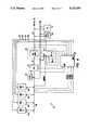
- FIG. 1is a simplified block diagram of a multiprocessor computer system incorporating the symmetric interrupt controller configuration of the present invention
- FIG. 2is a block diagram of a specific implementation of the symmetric configuration
- FIG. 3is a logic schematic of the symmetric configuration's PIC control logic
- FIG. 4is a logic schematic of one of the symmetric configuration's secondary PICs
- FIG. 5is a simplified block diagram of a multiprocessor computer system incorporating the asymmetric interrupt controller configuration of the present invention
- FIG. 6is a block diagram of a specific implementation of the asymmetric configuration.
- FIG. 7is a logic schematic of the asymmetric configuration's interrupt control logic.
- Appendix 1describes the system bus (NexBus) signals
- Appendix 2sets forth the AD-bus format during the address/status phase
- Appendix 3sets forth the interrupt assignments
- Appendix 4sets forth the PAL equations for the symmetric configuration interrupt control logic
- Appendix 5sets forth the PAL equations for the asymmetric configuration interrupt control logic.
- the following description of the techniques for handling interrupts in a multiprocessor environmentdeals with two configurations, referred to as the symmetric configuration and the asymmetric configuration.
- the primary CPU and the secondary CPUseach have a programmable interrupt controller (PIC).
- PICprogrammable interrupt controller
- the asymmetric configurationonly the primary CPU has a PIC, and other mechanisms are provided to generate interrupts and to provide an interrupt vector in response to an interrupt acknowledge operation.
- the same reference numeralswill be used for elements that are the same as those in the symmetric configuration, while primed reference numerals will be used for those elements that generally correspond.
- FIG. 1is a simplified block diagram of a computer system 10 incorporating the symmetric multiprocessor configuration of the present invention.
- CPUsprocessing units
- PICsprogrammable interrupt controllers
- FIG. 1shows four CPUs 15a-d and their associated PICs 20a-d.
- CPU 15ais referred to as the primary CPU and CPUs 15b-d are referred to as the secondary CPUs. Similar nomenclature applies to PIC 20a and PICs 20b-d. Signals and other references pertaining to a particular CPU or PIC will sometimes have suffixes 0-3 corresponding to the suffixes a-d on the reference numerals.
- the systemalso includes interrupt supervisory logic 22, general support logic 23, and a number of peripherals including a disk controller 25 and a keyboard controller 27.
- the CPUs, PICs, and peripheralscommunicate with each other via a number of buses and control lines, including an address bus 32, a data bus 35, a set of interrupt request (IRQ) lines 37, and a set of Master ID (MID) lines 40.
- PICs 20a-dcommunicate interrupts to their respective CPUs on interrupt lines 45a-d.
- Each of the CPUsis coupled to the address and data buses in the normal fashion.
- Each CPUwhen it is controlling the address and data buses, drives a code unique to itself on MID bus 40.
- the codecorresponds to the CPU's slot ID.
- Each PICis coupled to data bus 35 and at least some of IRQ lines 37.
- Each of the peripheralsis coupled to the address and data buses in the normal fashion, and to a selected IRQ line.
- Interrupt supervisory logic 22receives signals from the MID lines, address information either directly from the address bus or as decoded by support logic 23, and other control signals and configuration information from the support logic. Logic 22 communicates with PICs 20a-d via respective radial sets 47a-d of PIC control lines. As will be seen below, it is convenient to refer to interrupt supervisory logic 22 and secondary PICs 15b-d collectively as the multiprocessor interrupt control logic, referred to as MPIC 50, since it is the MPIC that provides the multiprocessor interrupt support.
- the CPUUpon receiving an interrupt from its associated PIC, the CPU performs a first interrupt acknowledge operation to latch the state of its associated PIC and a second operation to transfer the interrupt vector from the PIC to the CPU via the data bus. The CPU then proceeds to service the interrupt request by executing an interrupt handler pointed to by the interrupt vector.
- interruptsmay be responded to by more than one PIC.
- more than one CPUreceives the interrupt, and separate mechanisms are provided (typically by the operating system software) to allow an interrupted CPU to determine whether or not it is to service the interrupt.
- Other interruptsmay be responded to by only one PIC, in which case only one CPU receives the interrupt, and proceeds to service it.
- FIG. 2is a block diagram of a particular implementation of computer system 10 incorporating the symmetric configuration. Elements corresponding to those in FIG. 1 will be shown with corresponding reference numerals.
- each of CPUs 15a-dincludes an Intel 80386 microprocessor or the like and an associated numeric co-processor, and is coupled through a suitable bus interface to a proprietary system bus 60, sometimes referred to as the NexBus. Devices coupled via such bus interfaces to the NexBus are referred to as NexBus adapters.
- the bus linesare implemented as signal traces on a backplane circuit board referred to as a motherboard, and the adapters and at least some control logic are built on circuit boards, which are plugged into connectors on the motherboard.
- the connectorsare referred to as slots and are numbered from 0 to 15.
- Each slotsupports 4 sub-slots, which may correspond to separate functional units contained on a single adapter board (as determined by the type of primary functional unit in sub-slot 0).
- Appendix 1provides a description of the NexBus signals.
- the signal names in the appendices and schematicshave a minus sign prefix or an asterisk suffix foractive low signals.
- NexBus 60includes a 64-bit multiplexed address and data bus (AD-Bus). Bit positions on the AD-bus are numbered from 63 (most significant) to 0 (least significant).
- a NexBus master(such as one of the CPUs) communicates address and status in one bus phase, and the master or the addressed slave communicates data in a data phase, not necessarily in the same bus cycle.
- Appendix 2sets forth the information that is communicated during the address/status phase.
- the MID linesare AD ⁇ 45:40>, allowing the specification of 16 slots, each with 4 sub-slots.
- a 3-bit OPTYPE field AD ⁇ 48:46>specifies the type of bus operation.
- the adaptersinclude: CPU 15a, referred to as the primary CPU, in slot 15; CPUs 15b-d, referred to as secondary CPUs, in slots 14, 13, and 12; and an alternate bus interface (ABI) 65.
- the ABIis defined to occupy slot 0 although it is physically part of the motherboard logic.
- Other adapterswould include one or more memory subsystems shared between the processors, and optional high-speed I/O devices.
- Adapters plugged into the NexBus slotsare initialized through memory mapped registers that are located in the upper ranges of the 4GB memory space. Accesses to these locations enable the system to determine what type of device is plugged into the slot, and to configure each adapter.
- the address range for system initializationis from (4GB-16MB) or FF000000 to (4GB-8MB-1) or FF7FFFFF. This 8MB area is divided into 16 regions, each corresponding to a slot. Each region is subdivided into four sub-slot regions, each of which has a memory space of 32 4KB pages.
- the processorsinitialize themselves by reading their own SLOTID bits to determine whether they are primary or secondary CPUs, and branch accordingly to the proper POST (Power On Self Test) code.
- POSTPower On Self Test
- ABI 65couples the NexBus to a bus 75, referred to as the 386 bus, that has the same protocol as the local buses on an Intel 80386 microprocessor.
- the interface between the 386 bus and the MCA-busis provided by a Microchannel Interface (MCI) 80, which provides the logic support for a 386-based system using the MCA.
- MCIMicrochannel Interface
- MCI 80is part of the motherboard logic and is implemented in a commercially available chip set, namely a Chips and Technologies CHIPS/280 PS/2 Model 70/80 compatible chip set.
- the chip setincludes an 82C226 System Peripheral Chip, which provides a PIC as well as other peripheral functions. This is shown as primary PIC 20a, and in a typical prior art system would be the only PIC.
- Secondary PICs 20b-d and interrupt supervisory logic 22are part of MPIC 50, which supports the multiprocessor interrupts.
- the MPICis coupled to AB 70 and is further responsive to certain NexBus and MCA-bus signals, signals derived from them, and other signals from the ABI.
- MPIC 50may be implemented on the motherboard or on a small circuit board that plugs into a connector on the motherboard.
- Additional support logic 95 on the motherboard, associated with the ABI,provides an attention (ATTN) facility wherein any master can gain the attention of any of the CPUs.
- APNattention
- each of the CPU sub-slot regionscontains 32 pages. Any read operation to any address in page 3 sets an ATTN flag in the motherboard logic dedicated to support that processor slot, and any write to any address in page 3 clears the ATTN flag.
- the primary CPUsets up the page map table to specify which CPU(s) have read and write access to page 3 of the various sub-slot regions. In one typical configuration, read access will be given to all CPUs but write access only to the CPU corresponding to that sub-slot. Thus, in this configuration any CPU can set any other CPU's ATTN flag, but a CPU can only clear its own ATTN flag.
- Appendix 3is a list of the interrupt assignments.
- -IRQ ⁇ 3:7,9:12,14:15>are shared interrupts for devices such as disk controllers and serial ports. They are available as lines on the NexBus and the MCA-bus and are level sensitive, meaning that they may be easily shared by use of open collector drivers.
- system interrupt requestsinclude a periodic timer (-IRQ ⁇ 0>), a real time clock (-IRQ ⁇ 8>), and a numeric processor (NP) error indicator (-NPIRQ).
- NPnumeric processor error indicator
- the sources of these interruptsare duplicated for each CPU, and each CPU can access and respond to only its own timer, clock, and NP.
- -IRQ ⁇ 1>is available only to primary CPU 15a.
- AISATTN IRQ Select
- -IRQ ⁇ 13>has the advantage of a low level of usage and so it makes a good fallback position if -IRQ ⁇ 11> cannot be used.
- FIG. 3is a logic schematic of interrupt supervisory logic 22 within MPIC 50.
- Logic 22preferably comprises four programmable array logic (PAL) devices 101, 102, 103, and 104, programmed for operation as described below.
- PALprogrammable array logic
- PAL 101is coupled to the XA-bus (local I/O address bus on the MCA-bus) and provides a Select bit for address redirection.
- the purpose of address redirectionis to allow all the CPUs to access the non-PIC peripherals (real time clock, printer port, etc.) in a single System Peripheral Chip, namely the one on the motherboard.
- the address redirectionis not implemented, and the Select bit is set to 1.
- PAL 102receives latched versions of the NexBus MID lines as well as OBIOP and INTA signals from the MCI.
- OBIOPis derived from the I/O address and specifies an access to the System Peripheral chips.
- PAL 102provides radial OBIOP and INTA signals to a selected one of the four PICs.
- An optionis provided for CPU 15a to assert the radial OBIOP for any of PICs 20b-d depending on the value of a 2-bit register SETUP -- SEL on the NexBus side of the motherboard.
- a value of 0specifies normal operation where each CPU (including CPU 15a) accesses its own PIC only.
- PIC 20ais also selected in the event that a master on the MCA-bus asserts HLDA386.
- PAL 103generates ATTN interrupts for the CPUs.
- a 2-bit IRQSEL signalspecifies the particular CPU to be interrupted.
- An ATTN strobe signal generated by the ABIvalidates the setting or clearing of the ATTN interrupts, and a write signal (W/-R) derived from OPTYPE on the NexBus determines whether the ATTN is to be set or cleared.
- W/-Rwrite signal derived from OPTYPE on the NexBus determines whether the ATTN is to be set or cleared.
- -INTSENSEis a pin connected to ground on MPIC 50 and pulled up on MCI 80. This allows the system to determine whether an MPIC board is present. When the MPIC is absent, all PIC accesses are routed to the primary PIC.
- the -NPIRQ signals from the secondary CPUsare also communicated on the respective radial -IRQ13 lines while -NPIRQ0 is communicated directly to the -IRQ ⁇ 13> input on PIC 20a. This is shown as a wire OR in FIG. 2 since open collector devices are used.
- FIG. 4is a logic schematic of one of the secondary PICs, say PIC 20b.
- PICs 20c and 20dare connected the same way except that they receive their own respective signals corresponding to -OBIOP1, -INTA1, -IRQ11-1, and -IRQ13-1; provide their own respective signals corresponding to AUDIO1 and INTR1; and have their own pullups.
- FIG. 5is a simplified block diagram of a computer system 10' incorporating the asymmetric multiprocessor configuration of the present invention.
- the systemis shown with four CPUs 15a-d, but unlike the symmetric configuration discussed above, only primary CPU 15a has an associated PIC 20a.
- the systemalso includes interrupt supervisory logic 22', general support logic 23, and a number of peripherals.
- the CPUs, PIC, and peripheralscommunicate with each other via an address bus 32, a data bus 35, a set of IRQ lines 37, and a set of MID lines 40.
- PIC 20acommunicates interrupts to CPU 15a on an interrupt line 45a
- interrupt supervisory logic 22'communicates interrupts to CPUs 15b-d on a set of interrupt lines 45b'-45d'.
- the various elementsare shown to be connected to the buses and lines as in the symmetric configuration.
- Interrupt supervisory logic 22'receives signals from the MID lines, address information either directly from the address bus or is decoded by support logic 23, and other control signals and configuration information from the support logic. Logic 22' communicates with PIC 20a via a set 47a' of PIC control lines. Logic 22' is coupled to a vector generator 48. Logic 22' and vector generator 48 together define MPIC 50'.
- Possible sources of interrupts for primary CPU 15aare communicated to PIC 20a while potential sources for interrupts for the secondary CPUs are communicated to the interrupts supervisory logic 22', which, as noted above, communicates interrupt to the secondary CPUs.
- the primary CPUUpon receiving an interrupt, the primary CPU performs interrupt acknowledge operations and the PIC transfers the interrupt vector to the CPU via the data bus. This is the same as in the case of the symmetric configuration. However, in the asymmetric configuration, the secondary CPUs have no PICs.
- the interrupt supervisory logicdetermines (on the basis of the MID lines) that an interrupt acknowledge operation is being initiated by one of the secondary CPUs, logic 22' causes vector generator 48 to write a fixed interrupt vector onto the data bus.
- FIG. 6is a block diagram of a particular implementation of computer system 10' incorporating the asymmetric configuration.
- the diagram at this levelis very similar to the block diagram of FIG. 2, except that MPIC 50' is not coupled to all the shared interrupt lines, since it does not contain PICs. MPIC 50' still receives the NPIRQ and ATTN interrupts.
- FIG. 7is a logic schematic of interrupt supervisory logic 22' and vector generator 48 within MPIC 50'.
- Logic 22'preferably comprises four PAL devices 120, 122, and 125, programmed for operation as described below.
- Vector generator 48is also preferably implemented as a PAL device. The PAL equations are set forth in Appendix 5.
- PAL 120corresponds generally to PAL 102 in the symmetric MPIC. It receives latched versions of the MID lines and the OBIOP and INTA signals, and based on this provides INTA0 and OBIOP0 signals to PIC 20a when the MID field signifies the primary CPU and an INTA signal to vector generator 48 when the MID field indicates a secondary CPU.
- PALs 122 and 125together perform operations corresponding generally to PALs 103 and 104 together in the symmetric MPIC.
- PAL 122derives four ATTN signals.
- One, ATTN0is used to enable IRQ11 and IRQ13 lines to PIC 20a, while the other three, ATTN1, ATTN2, and ATTN3, are input to PAL 125.
- PAL 125receives the NPIRQ signals from the secondary processors, and combines them with the secondary ATTN signals to provide interrupt signals -INTR1, -INTR2, and -INTR3, which are communicated to the interrupt inputs of secondary CPUs.
- the present inventionprovides a flexible and transparent interrupt support for multiprocessor computer systems.
- vector generator 48 in the asymmetric configurationcould be a programmable register rather than a hardwired one.
- separate vector registerscould be provided for the secondary CPUs.
- AD ⁇ 63:0>Address, Status and Data bits 63 through 0: This bus conveys either address and status or data.
- AD ⁇ 63:0>contains address and status information defining a bus operation.
- this buscontains up to 64 bits of data.
- -ALE[n]Address Latch Enable: The -ALE[n] signals are issued by the master.
- the GALE signalis monitored by all devices on the NexBus to latch the address placed on the bus by the master.
- -AREQ[n]The Alternate Bus Request signals are driven by would-be masters on the NexBus to secure bus mastership together with control of the AB.
- the arbiterexamines these signals together with the -NREQ signals (q.v.) and the state of the Alternate Bus Interface to determine which device is to be granted mastership of the NexBus. It also passes AB requests to the ABI to cause it to gain control of the AB.
- the requesting devicesdrive these signals active at the rising edge of the BCLK.
- AUDIOThis is an audio sum node used to drive audio signals from an adapter to the system audio output, or to transfer audio signals between adapters.
- This lineis electrically compatible with the similar line defined on the Microchannel bus, and in a system having a Microchannel bus as an AB it may be electrically connected to the Microchannel's AUDIO line.
- AUDIO GNDThis is a separate ground for the audio subsytem. It must never be connected to system GND at any point except the subsystem's audio amplifier (radial grounding).
- +/-BCLKare the TTL-level bus clock and its inversion which define the NexBus clock period. They are received on each board by a clock chip and are terminated on-board by a 180 ohm resistor connecting +BCLK to -BCLK.
- -CACHBL[n]GCACHBL: Cacheable: The -CACHBL[n] signals are driven active by slaves to indicate that portions of their address space may be cacheable. The ABI may drive this signal as non-cacheable to indicate that all the devices on the Alternate Bus are non-cacheable. If a slave does not assert its -CACHBL signal, it cannot support block transfers.
- -CHCHKChannel Check is generated on the adapters on the NexBus upon detection of a systemwide error condition. It is gated by logic in the ABI to cause the -NMI pin of the primary processor on the NexBus to be asserted.
- GDCLDirty Cache Lock
- the -DCL[n] signalsare issued by all the caching devices on the bus. The purpose of this signal is to let the caching devices indicate that the current read or write operation hit in a dirty cache block.
- GDCLindicates to the master that data supplied by the slave is stale.
- the -DCL linesare used to preemptively gain control of the bus so that the intervenor can supply updated memory to the requestor and to memory by doing a block write.
- GATEA20This signal, which exists only on the Primary Processor slot, slot 0Fh, is driven by the ABI and received by the primary processor. When this signal is active, the processor drives bit 20 of the address line to any desired value. When this bit is inactive bit 20 of the address is set to zero. The purpose of this signal is to replicate the method in which IBM PC's work around an 80286 bug in implementing address wrap around for addresses above the address limit.
- the Bus Grant signalsare driven by the arbiter to the arbitrating devices on the NexBus to indicate that the bus has been granted to the requesting device. These signals are driven active at the rising edge of the BCLK.
- the Hold Bus for 32-Bit Transfer signalsare asserted by a 32-bit wide device receiving data (either a master performing a read operation or a slave in a write operation) to tell the arbiter not to immediately re-grant the bus after the fall of GXACK and to cause the swapping logic to latch and transfer the high-order four bytes of data from AD ⁇ 63:32> onto AD ⁇ 31:0>.
- the Interrupt signalsare generated by the interrupt controllers on the ABI and dispatched radially to each processor slot (primary or secondary) on the NexBus.
- -IRQ ⁇ 3:7,9:12,14:15>The Interrupt Request signals are logically combined with the interrupt request lines on the AB, and are used by individual devices on the NexBus to gain the attention of a processor.
- Certain interrupt levelsare pre-defined: -IRQ ⁇ 0> is a periodic interrupt from the system timers; -IRQ ⁇ 1> is the interrupt from the Keyboard Controller; -IRQ ⁇ 2> is an internal cascade signal from one interrupt controller to another and is not available for use; -IRQ ⁇ 8> is used as a general purpose interrupt from the Real Time Clock.
- -IRQ ⁇ 13>is derived from -NPIRQ[n] lines (as described below). Therefore, only levels 3:7,9:12, and 14:15 are available as lines on the NexBus.
- -LATCH32[n]The Latch 32 Bits of Data signals are driven by a 32-bit wide data provider (a master doing a write operation or a slave in a read operation) to cause the swapping logic to latch the contents of AD ⁇ 31:0> and transfer it to AD ⁇ 63:32>.
- -NMIThe Non-Maskable Interrupt, which exists only on the Primary Processor slot, SlotID 0Fh, is generated by the ABI in response to any of several error conditions, including -CHCHK on the NexBus or Alternate Bus. It drives the -NMI pin of the primary processor on the NexBus.
- the NexBus Request signalsare driven by the masters on the NexBus.
- the arbiterexamines them in conjunction with the -AREQ lines and the state of the ABI to arbitrate bus mastership at the end of each bus sequence. At any time one or more of these signals may be active, requesting the bus, but only one can be granted the NexBus.
- the bus request signalsnormally remain active until the corresponding grant line goes active.
- the requesting devicesdrive these signals active at the rising edge of the BCLK.
- the Reset signalis driven by the bus backplane and received by all the devices on the bus. The purpose of this signal is to reset all the adapters on the NexBus. It is redundant, since the same information is contained on the SR signal.
- the Reset CPU signalwhich exists only on the Primary Processor slot, slotID 0Fh, is generated by the ABI and received by the primary processor. The purpose of the this signal is to reset one designated processor.
- GSHAREShared Data: The -SHARE[n] signals are issued by all the caching devices on the bus. The purpose of this signal is to let the caching devices indicate that the current read operation hit in a cache block that is present in another device's cache. During reads, GSHARE indicates to the master that data being read must be cached as SHARED (if cached at all), unless the master has asserted -OWN (transmitted on AD ⁇ 49> during the address/status phase of a bus operation). The state of GSHARE must be ignored during any operations with -OWN asserted.
- the Sync/Reset signalwhich originates in the master Clock Distribution (CDIS) chip, is distributed radially on the backplane. It conveys a serial code which includes timing information to synchronize all CDIS chips on all adapters. It also conveys the System RESET signal and bus operating frequency information.
- CDISmaster Clock Distribution
- SLOTID ⁇ 3:0>Slot ID bits 3 through 0 are encoded on the connector to geographically distinguish one slot from another. This will allow the NexBus to have a maximum of sixteen slots.
- the Try Again Later signalindicates to the master that the current operation cannot be completed at this time because the AB is not available.
- the TAL signalis transmitted by the ABI, and monitored by all master devices on the NexBus. Upon detecting an active TAL, the master will abort the current operation and will re-try it later. In order to secure the bus for re-trying the operation, the master must assert its -AREQ, thereby assuring that the AB will be available when it is re-granted the bus.
- GXACKTransfer Acknowledge:
- the -XACK[n] signalsare driven by the slave after it has decoded the address and determined that it is a party in the current operation.
- the ABImonitors GXACK to determine whether a NexBus device responds to an address within three clocks, to decide whether it needs to perform a crossing operation.
- the mastermonitors GXACK and GXHLD to determine when data is available on the bus.
- the masteragain monitors these signals to determine when data is accepted by the slave.
- -XHLD[n]Transfer Hold:
- the -XHLD[n] signalsmay be driven by the master, the slave, or by a third party monitoring an operation, in order to insert wait states into an operation. Both master and slave must monitor GXHLD to synchronize data transfer.
- ADRS ⁇ 2>is used as the least-significant 4-byte Word address for I/O operations. It is not used for memory-reference operations and may be driven to either defined state (either 0 or 1).
- ADRS ⁇ 15:3>specifies a DWord address within the 64-Kbyte I/O address space for I/O operations, and AD ⁇ 31:16> must be 0.
- Byte-Enable bits 7 through 0are framing bits associated with the data of the current bus operation.
- -BE ⁇ 7:4>are not used and must be driven high (inactive), while -BE ⁇ 3:0> specify the byte(s) to be transferred on AD ⁇ 31:0>.
- a memory operationall eight bits are used to specify the byte(s) to be transferred on AD ⁇ 63:0>.
- the BE'sIn a multi-DWord block transfer operation the BE's have meaning only for the first DWord of the transfer, and only for write operations; the rest of the DWords have implicit byte enable bits of all 0's, i.e., all bytes are to be transferred in each of the other DWords. Even if a master is requesting a block read operation, it should use the BE's to specify the bytes that it needs immediately, since a non-cacheable slave may force a single-DWord transfer operation and then needs only to return to the master only those bytes for which BE's are asserted.
- AD ⁇ 48:46>: OP -- TYPE ⁇ 2:0>are driven by the master to define the type of operation to be performed. Note that AD ⁇ 48:46> have the same meaning that these signals have in the 80386 microprocessor.
- AD ⁇ 49>: -OWNmay be driven active during read or write operations. This signal is driven by the master during such operations requesting the ownership of data in its cache. If this operation hits in the cache of another caching master, then that master must change the status of its cache line to the ABSENT, rather than SHARED, state.
- these two bitsdefine the size of data requested to be transferred in the operation, as shown in Table 2, below.
- the bytes to be transferred in the first DWordhence, the size of the transfer, can be specified by the Byte Enable bits described above. Note that if the slave is incapable of transferring more than a single DWord it may deny a request for a larger block by negating its XACK signal after a single DWord, or the bytes thereof specified by the Byte Enable bits, have been transferred. These bits should be "1" for I/O operations.
Landscapes
- Engineering & Computer Science (AREA)
- Theoretical Computer Science (AREA)
- Physics & Mathematics (AREA)
- General Engineering & Computer Science (AREA)
- General Physics & Mathematics (AREA)
- Bus Control (AREA)
Abstract
Description
______________________________________ AD<48> AD<47> AD<46> BUS M/-IO D/-C W/-R OPERATION TYPE ______________________________________ 0 0 0 INTERRUPTACK 0 0 1 HALT,SHUTDOWN 0 1 0 I/O DATA READ 0 1 1 I/O DATA WRITE 1 0 0MEM CODE READ 1 0 1 HALT,SHUTDOWN 1 1 0MEM DATA READ 1 1 1 MEM DATA WRITE ______________________________________
______________________________________ -BLOCK4 -BLOCK2 AD<51> AD<50> BLOCK SIZE ______________________________________ 1 1 Single DWord (0 to 8 bytes) 1 0 2-DWord Block (8 to 16 bytes) 0 1 4-DWord Block (24 to 32 bytes) 0 0 not used: Specified as "don't care" ______________________________________
__________________________________________________________________________Request Meaning Notes __________________________________________________________________________-IRQ<0> Periodic Timer Interrupt per-CPU timers -IRQ<1> Keyboard Interface Ctrl. -IRQ<2> Not Used Cascade from -IRQ<15:8> -IRQ<3>Serial Port 2 Depends on System Conf. -IRQ<4>Serial Port 1 Depends on System Conf. -IRQ<5>Parallel Port 2 Depends on System Conf. -IRQ<6> Diskette Controller -IRQ<7>Parallel Port 1 Depends on System Conf. -IRQ<8> Real-Time Clock per-CPU clock -IRQ<9> Unassigned -IRQ<10> Unassigned -IRQ<11> ATTN (Primary, AIS=0) common -IRQ<11> line -IRQ<12> Mouse Interface Ctrl. -IRQ<13> Numeric Proc./ Alt. ATTN per-CPU -IRQ<14> Fixed Disk Controller -IRQ<15> Unassigned __________________________________________________________________________
__________________________________________________________________________U1 - Address Decode (Symmetric) Inputs: XA0 Outputs: SELECT XA1 XA2 XA3 XA4 XA5 XA6 XA7 XA8 XA9 Equations SELECT = 1 Symbol Meanings: & signifies logical AND. # signifies logical OR. U2 - Interrupt Control (Symmetric) Inputs: MID2 Outputs: -INTA0 MID3 -INTA1 MID4 -INTA2 MID5 -INTA3 -INTA -OBIOP0 -OBIOP -OBIOP1 SETUP.sub.-- SEL0 -OBIOP2 SETUP.sub.-- SEL1 -OBIOP3 HLDA386 SELECT Declarations SETUP = SETUP.sub.-- SEL<1:01> ID = MID<5:2> OPER.sub.-- MODE = (SETUP .EQ. 0) SETUP.sub.-- PIC1 = (SETUP .EQ. 1) SETUP.sub.-- PIC2 = (SETUP .EQ. 2) SETUP.sub.-- PIC3 = (SETUP .EQ. 3) CPU0 = (ID .EQ. 15) CPU1 = (ID .EQ. 14) CPU2 = (ID .EQ. 13) CPU3 = (ID .EQ. 12) Equations INTA0 = CPU0 & INTA INTA1 = CPU1 & INTA INTA2 = CPU2 & INTA INTA3 = CPU3 & INTA OBIOP0 = OBIOP & CPU0 & OPER.sub.-- MODE # OBIOP & HLDA386 OBIOP1 = OBIOP & CPU0 & SETUP.sub.-- PIC1 # OBIOP & CPU1 & OPER.sub.-- MODE & SELECT OBIOP2 = OBIOP & CPU0 & SETUP.sub.-- PIC2 # OBIOP & CPU2 & OPER.sub.-- MODE & SELECT OBIOP3 = OBIOP & CPU0 & SETUP.sub.-- PIC3 # OBIOP & CPU3 & OPER.sub.-- MODE & SELECT U3 - Attention Control (Symmetric) Inputs: IRQSEL0 Outputs: ATTN0 IRQSEL1 ATTN1 W.sub.-- R ATTN2 ATTN.sub.-- STB ATTN3 RESET4 INTSENSE Declarations IRQ.sub.-- SEL = IRQSEL <0:1> ATTN.sub.-- SET = (ATTN.sub.-- STB & -W.sub.-- R) ATTN.sub.-- CLR = (ATTN.sub.-- STB & W.sub.-- R) SET0 = ( (IRQ.sub.-- SEL .EQ. 0) & ATTN.sub.-- SET ) SET1 = ( (IRQ.sub.-- SEL .EQ. 1) & ATTN.sub.-- SET ) SET2 = ( (IRQ.sub.-- SEL .EQ. 2) & ATTN.sub.-- SET ) SET3 = ( (IRQ.sub.-- SEL .EQ. 3) & ATTN.sub.-- SET ) RESET0 = ( (IRQ.sub.-- SEL .EQ. 0) & ATTN.sub.-- CLR ) # RESET4 RESET1 = ( (IRQ.sub.-- SEL .EQ. 1) & ATTN.sub.-- CLR ) # RESET4 RESET2 = ( (IRQ.sub.-- SEL .EQ. 2) & ATTN.sub.-- CLR ) # RESET4 RESET3 = ( (IRQ.sub.-- SEL .EQ. 3) & ATTN.sub.-- CLR ) # RESET4 Equations INTSENSE = 0 WHEN ( RESET0 ) THEN ATTN0 = 0 WHEN ( RESET1 ) THEN ATTN1 = 0 WHEN ( RESET2 ) THEN ATTN2 = 0 WHEN ( RESET3 ) THEN ATTN3 = 0 WHEN ( -RESET0 & SET0 ) THEN ATTN0 = 1 WHEN ( -RESET1 & SET1 ) THEN ATTN1 = 1 WHEN ( -RESET2 & SET2 ) THEN ATTN2 = 1 WHEN ( -RESET3 & SET3 ) THEN ATTN3 = 1 WHEN ( -RESET0 & -SET0 ) THEN ATTN0 = ATTN0 WHEN ( -RESET1 & -SET1 ) THEN ATTN1 = ATTN1 WHEN ( -RESET2 & -SET2 ) THEN ATTN2 = ATTN2 WHEN ( -RESET3 & -SET3 ) THEN ATTN3 = ATTN3 (RESET overrides SET) U4 - Interrupt Generation (Symmetric) Inputs: INTR.sub.-- 13.sub.-- 11 Outputs: -IRQ11OUT ATTN0 -IRQ11.sub.-- 1 ATTN1 -IRQ11.sub.-- 2 ATTN2 -IRQ11.sub.-- 3 ATTN3 IRQ13OUT -NPIRQ1 -IRQ13.sub.-- 1 -NPIRQ2 -IRQ13.sub.-- 2 -NPIRQ3 -IRQ13.sub.-- 3 -IRQ11IN Equations IRQ11OUT = (ATTN0 & -INTR.sub.-- 13.sub.-- 11) # IRQ11IN IRQ11.sub.-- 1 = (ATTN1 & -INTR.sub.-- 13.sub.-- 11) # IRQ11IN IRQ11.sub.-- 2 = (ATTN2 & -INTR.sub.-- 13.sub.-- 11) # IRQ11IN IRQ11.sub.-- 3 = (ATTN3 & -INTR.sub.-- 13.sub.-- 11) # IRQ11IN IRQ13OUT = 0 ENABLE IRQ13OUT = (ATTN0 & INTR.sub.-- 13.sub.-- 11) IRQ13.sub.-- 1 = (ATTN1 & INTR.sub.-- 13.sub.-- 11) # NPIRQ1 IRQ13.sub.-- 2 = (ATTN2 & INTR.sub.-- 13.sub.-- 11) # NPIRQ2 IRQ13.sub.-- 3 = (ATTN3 & INTR.sub.-- 13.sub.-- 11) # NPIRQ3 __________________________________________________________________________
__________________________________________________________________________U1 - Attention Control (Asymmetric) Inputs: IRQSEL0 Outputs: ATTN0 IRQSEL1 ATTN1 W.sub.-- R ATTN2 ATTN.sub.-- STB ATTN3 RESET4 -IRQ11OUT INTR13/11 -IRQ13OUT RESET4 Declarations IRQ.sub.-- SEL = IRQSEL <0:1> ATTN.sub.-- SET = (ATTN.sub.-- STB & -W.sub.-- R) ATTN.sub.-- CLR = (ATTN.sub.-- STB & W.sub.-- R) SET0 = ( (IRQ.sub.-- SEL .EQ. 0) & ATTN.sub.-- SET ) SET1 = ( (IRQ.sub.-- SEL .EQ. 1) & ATTN.sub.-- SET ) SET2 = ( (IRQ.sub.-- SEL .EQ. 2) & ATTN.sub.-- SET ) SET3 = ( (IRQ.sub.-- SEL .EQ. 3) & ATTN.sub.-- SET ) RESET0 = ( (IRQ.sub.-- SEL .EQ. 0) & ATTN.sub.-- CLR ) # RESET4 RESET1 = ( (IRQ.sub.-- SEL .EQ. 1) & ATTN.sub.-- CLR ) # RESET4 RESET2 = ( (IRQ.sub.-- SEL .EQ. 2) & ATTN.sub.-- CLR ) # RESET4 RESET3 = ( (IRQ.sub.-- SEL .EQ. 3) & ATTN.sub.-- CLR ) # RESET4 Equations WHEN ( RESET0 ) THEN ATTN0 = 0 WHEN ( RESET1 ) THEN ATTN1 = 0 WHEN ( RESET2 ) THEN ATTN2 = 0 WHEN ( RESET3 ) THEN ATTN3 = 0 WHEN ( -RESET0 & SET0 ) THEN ATTN0 = 1 WHEN ( -RESET1 & SET1 ) THEN ATTN1 = 1 WHEN ( -RESET2 & SET2 ) THEN ATTN2 = 1 WHEN ( -RESET3 & SET3 ) THEN ATTN3 = 1 WHEN ( -RESET0 & -SET0 ) THEN ATTN0 = ATTN0 WHEN ( -RESET1 & -SET1 ) THEN ATTN1 = ATTN1 WHEN ( -RESET2 & -SET2 ) THEN ATTN2 = ATTN2 WHEN ( -RESET3 & -SET3 ) THEN ATTN3 = ATTN3 IRQ11OUT = 0 ENABLE IRQ13OUT = (ATTN0 & -INTR.sub.-- 13.sub.-- 11) IRQ13OUT = 0 ENABLE IRQ13OUT = (ATTN0 & INTR.sub.-- 13.sub.-- 11) Symbol Meanings: & signifies logical AND. # signifies logical OR. U2 - Interrupt Generation (Asymmetric) Inputs: ATTN1 Outputs: -INTR1 ATTN2 -INTR2 ATTN3 -INTR3 -NPIRQ1 -NPIRQ2 -NPIRQ3 Equations INTR1 = ATTN1 # NPIRQ1 INTR2 = ATTN2 # NPIRQ2 INTR3 = ATTN3 # NPIRQ3 U3 - Interrupt Control (Asymmetric) Inputs: MID2 Outputs: -INTA0 MID3 -INTA1 MID4 -OBIOP0 -INTA -INTSENSE -OBIOP Declarations SETUP = SETUP.sub.-- SEL<1:01> ID = MID<5:2> OPER.sub.-- MODE = (SETUP .EQ. 0) SETUP.sub.-- PIC1 = (SETUP .EQ. 1) SETUP.sub.-- PIC2 = (SETUP .EQ. 2) SETUP.sub.-- PIC3 = (SETUP .EQ. 3) CPU0 = (ID .EQ. 15) CPU1 = (ID .EQ. 14) CPU2 = (ID .EQ. 13) CPU3 = (ID .EQ. 12) Equations INTA0 = CPU0 & INTA INTA1 = -CPU0 & INTA OBIOP0 = OBIOP INTSENSE = 0 U4 - Interrupt Vector (Asymmetric) Inputs: INTA1 Outputs: XD<7:0> Declaration XD = XD<7:0> Equations XD = 80 (hex) ENABLE XD = INTA1 __________________________________________________________________________
Claims (16)
Priority Applications (2)
| Application Number | Priority Date | Filing Date | Title |
|---|---|---|---|
| US07/567,399US5125093A (en) | 1990-08-14 | 1990-08-14 | Interrupt control for multiprocessor computer system |
| PCT/US1991/005474WO1992003793A1 (en) | 1990-08-14 | 1991-08-01 | Interrupt control for multiprocessor computer system |
Applications Claiming Priority (1)
| Application Number | Priority Date | Filing Date | Title |
|---|---|---|---|
| US07/567,399US5125093A (en) | 1990-08-14 | 1990-08-14 | Interrupt control for multiprocessor computer system |
Publications (1)
| Publication Number | Publication Date |
|---|---|
| US5125093Atrue US5125093A (en) | 1992-06-23 |
Family
ID=24266995
Family Applications (1)
| Application Number | Title | Priority Date | Filing Date |
|---|---|---|---|
| US07/567,399Expired - Fee RelatedUS5125093A (en) | 1990-08-14 | 1990-08-14 | Interrupt control for multiprocessor computer system |
Country Status (2)
| Country | Link |
|---|---|
| US (1) | US5125093A (en) |
| WO (1) | WO1992003793A1 (en) |
Cited By (55)
| Publication number | Priority date | Publication date | Assignee | Title |
|---|---|---|---|---|
| US5265215A (en)* | 1991-04-22 | 1993-11-23 | International Business Machines Corporation | Multiprocessor system and interrupt arbiter thereof |
| US5283904A (en)* | 1990-12-21 | 1994-02-01 | Intel Corporation | Multi-processor programmable interrupt controller system |
| US5313640A (en)* | 1992-09-23 | 1994-05-17 | International Business Machines Corporation | Method and system for the efficient response to multiple different types of interrupts |
| US5317747A (en)* | 1990-03-08 | 1994-05-31 | Hitachi, Ltd. | Multiprocessor system and interruption control device for controlling interruption requests between processors and peripheral devices in the multiprocessor system |
| US5369769A (en)* | 1992-09-09 | 1994-11-29 | Intel Corporation | Method and circuitry for selecting a free interrupt request level from a multiplicity of interrupt request levels in a personal computer system |
| US5379434A (en)* | 1992-12-18 | 1995-01-03 | International Business Machines Corporation | Apparatus and method for managing interrupts in a multiprocessor system |
| US5404457A (en)* | 1992-02-14 | 1995-04-04 | Advanced Micro Devices, Inc. | Apparatus for managing system interrupt operations in a computing system |
| US5410710A (en)* | 1990-12-21 | 1995-04-25 | Intel Corporation | Multiprocessor programmable interrupt controller system adapted to functional redundancy checking processor systems |
| US5414820A (en)* | 1991-08-23 | 1995-05-09 | Nexgen, Inc. | Crossing transfers for maximizing the effective bandwidth in a dual-bus architecture |
| US5423049A (en)* | 1991-01-31 | 1995-06-06 | Nec Corporation | Multiprocessor circuit |
| US5428799A (en)* | 1991-02-13 | 1995-06-27 | Hewlett-Packard Company | Redirection of interrupts to microprocessors |
| US5481725A (en)* | 1993-08-03 | 1996-01-02 | Intel Corporation | Method for providing programmable interrupts for embedded hardware used with programmable interrupt controllers |
| US5517624A (en)* | 1992-10-02 | 1996-05-14 | Compaq Computer Corporation | Multiplexed communication protocol between central and distributed peripherals in multiprocessor computer systems |
| US5561772A (en)* | 1993-02-10 | 1996-10-01 | Elonex Technologies, Inc. | Expansion bus system for replicating an internal bus as an external bus with logical interrupts replacing physical interrupt lines |
| US5579523A (en)* | 1992-10-13 | 1996-11-26 | Sony Corporation | Method for controlled locking/unlocking of a system using a locking mode flag during an interrupt routine |
| US5581770A (en)* | 1992-06-04 | 1996-12-03 | Mitsubishi Denki Kabushiki Kaisha | Floating interruption handling system and method |
| US5594907A (en)* | 1992-10-13 | 1997-01-14 | Sony Corporation | Apparatus for locking/unlocking a number of units connected to a master unit |
| US5603035A (en)* | 1991-08-22 | 1997-02-11 | Telemecanique | Programmable interrupt controller, interrupt system and interrupt control process |
| US5613128A (en)* | 1990-12-21 | 1997-03-18 | Intel Corporation | Programmable multi-processor interrupt controller system with a processor integrated local interrupt controller |
| US5613126A (en)* | 1994-05-31 | 1997-03-18 | Advanced Micro Devices, Inc. | Timer tick auto-chaining technique within a symmetrical multiprocessing system |
| US5613129A (en)* | 1994-05-02 | 1997-03-18 | Digital Equipment Corporation | Adaptive mechanism for efficient interrupt processing |
| US5619705A (en)* | 1993-12-16 | 1997-04-08 | Intel Corporation | System and method for cascading multiple programmable interrupt controllers utilizing separate bus for broadcasting interrupt request data packet in a multi-processor system |
| US5634130A (en)* | 1993-09-20 | 1997-05-27 | International Business Machines Corporation | Method and apparatus for spurious interrupt detection in a data processing system |
| US5701495A (en)* | 1993-09-20 | 1997-12-23 | International Business Machines Corporation | Scalable system interrupt structure for a multi-processing system |
| US5768617A (en)* | 1991-08-07 | 1998-06-16 | Adaptec, Inc. | Intelligent hardware for automatically reading and writing multiple sectors of data between a computer bus and a disk drive |
| US5778236A (en)* | 1996-05-17 | 1998-07-07 | Advanced Micro Devices, Inc. | Multiprocessing interrupt controller on I/O bus |
| US5781187A (en)* | 1994-05-31 | 1998-07-14 | Advanced Micro Devices, Inc. | Interrupt transmission via specialized bus cycle within a symmetrical multiprocessing system |
| US5850555A (en)* | 1995-12-19 | 1998-12-15 | Advanced Micro Devices, Inc. | System and method for validating interrupts before presentation to a CPU |
| US5850558A (en)* | 1995-12-19 | 1998-12-15 | Advanced Micro Devices | System and method for referencing interrupt request information in a programmable interrupt controller |
| US5894578A (en)* | 1995-12-19 | 1999-04-13 | Advanced Micro Devices, Inc. | System and method for using random access memory in a programmable interrupt controller |
| US5905897A (en)* | 1997-03-20 | 1999-05-18 | Industrial Technology Research Institute | Method and apparatus for selecting a nonblocked interrupt request |
| US5918057A (en)* | 1997-03-20 | 1999-06-29 | Industrial Technology Research Institute | Method and apparatus for dispatching multiple interrupt requests simultaneously |
| US5931930A (en)* | 1994-06-29 | 1999-08-03 | Intel Corporation | Processor that indicates system bus ownership in an upgradable multiprocessor computer system |
| DE4413459C2 (en)* | 1993-04-19 | 2000-04-06 | Intel Corp | Programmable interrupt controller system |
| US6205508B1 (en)* | 1999-02-16 | 2001-03-20 | Advanced Micro Devices, Inc. | Method for distributing interrupts in a multi-processor system |
| US6249830B1 (en) | 1996-08-20 | 2001-06-19 | Compaq Computer Corp. | Method and apparatus for distributing interrupts in a scalable symmetric multiprocessor system without changing the bus width or bus protocol |
| US6295573B1 (en) | 1999-02-16 | 2001-09-25 | Advanced Micro Devices, Inc. | Point-to-point interrupt messaging within a multiprocessing computer system |
| US6338112B1 (en) | 1997-02-21 | 2002-01-08 | Novell, Inc. | Resource management in a clustered computer system |
| US6389526B1 (en) | 1999-08-24 | 2002-05-14 | Advanced Micro Devices, Inc. | Circuit and method for selectively stalling interrupt requests initiated by devices coupled to a multiprocessor system |
| US6430593B1 (en)* | 1998-03-10 | 2002-08-06 | Motorola Inc. | Method, device and article of manufacture for efficient task scheduling in a multi-tasking preemptive priority-based real-time operating system |
| US6557068B2 (en) | 1998-09-03 | 2003-04-29 | Hewlett-Packard Development Company, L.P. | High speed peripheral interconnect apparatus, method and system |
| US6606676B1 (en)* | 1999-11-08 | 2003-08-12 | International Business Machines Corporation | Method and apparatus to distribute interrupts to multiple interrupt handlers in a distributed symmetric multiprocessor system |
| US6681281B1 (en)* | 2000-11-17 | 2004-01-20 | Advanced Micro Devices, Inc. | System and method for implementing a multi-level interrupt scheme in a computer system |
| KR100399385B1 (en)* | 1995-03-21 | 2004-02-05 | 아드밴스트 마이크로 디이바이시스 인코포레이티드 | Multiprocessing system using adaptive interrupt mapping mechanism and method |
| US20040068598A1 (en)* | 2002-10-07 | 2004-04-08 | Renesas Technology Corp. | Multiprocessor system having interrupt controller |
| US6816934B2 (en) | 2000-12-22 | 2004-11-09 | Hewlett-Packard Development Company, L.P. | Computer system with registered peripheral component interconnect device for processing extended commands and attributes according to a registered peripheral component interconnect protocol |
| US20060112208A1 (en)* | 2004-11-22 | 2006-05-25 | International Business Machines Corporation | Interrupt thresholding for SMT and multi processor systems |
| US7225285B1 (en)* | 2004-09-07 | 2007-05-29 | Altera Corporation | Assigning interrupts in multi-master systems |
| US20070130567A1 (en)* | 1999-08-25 | 2007-06-07 | Peter Van Der Veen | Symmetric multi-processor system |
| US20070156941A1 (en)* | 2004-10-14 | 2007-07-05 | Dell Products L.P. | Method for synchronizing processors following a memory hot plug event |
| US7263567B1 (en)* | 2000-09-25 | 2007-08-28 | Intel Corporation | Method and apparatus for lowering the die temperature of a microprocessor and maintaining the temperature below the die burn out |
| US20080082710A1 (en)* | 2006-09-29 | 2008-04-03 | Dell Products L.P. | System and method for managing system management interrupts in a multiprocessor computer system |
| US20080168202A1 (en)* | 2007-01-05 | 2008-07-10 | International Business Machines Corporation | Directly initiating by external adapters the setting of interruption initiatives |
| US10684965B2 (en) | 2017-11-08 | 2020-06-16 | Advanced Micro Devices, Inc. | Method to reduce write responses to improve bandwidth and efficiency |
| US20220309026A1 (en)* | 2021-03-29 | 2022-09-29 | Foundation Of Soongsil University Industry Cooperation | Processor for processing external service requests using a symmetrical network interface |
Citations (6)
| Publication number | Priority date | Publication date | Assignee | Title |
|---|---|---|---|---|
| US4149243A (en)* | 1977-10-20 | 1979-04-10 | International Business Machines Corporation | Distributed control architecture with post and wait logic |
| US4495569A (en)* | 1982-06-28 | 1985-01-22 | Mitsubishi Denki Kabushiki Kaisha | Interrupt control for multiprocessor system with storage data controlling processor interrupted by devices |
| US4598356A (en)* | 1983-12-30 | 1986-07-01 | International Business Machines Corporation | Data processing system including a main processor and a co-processor and co-processor error handling logic |
| US4604500A (en)* | 1981-12-02 | 1986-08-05 | At&T Bell Laboratories | Multiprocessing interrupt arrangement |
| US4722048A (en)* | 1985-04-03 | 1988-01-26 | Honeywell Bull Inc. | Microcomputer system with independent operating systems |
| US4935866A (en)* | 1981-04-03 | 1990-06-19 | Compagnie Industrial Des Telecommunications Cit-Alcatel | Multiprocessor control system |
Family Cites Families (1)
| Publication number | Priority date | Publication date | Assignee | Title |
|---|---|---|---|---|
| US4495596A (en)* | 1982-06-10 | 1985-01-22 | Rockwell International Corporation | Data accumulator and transponder with power back-up for time of day clock |
- 1990
- 1990-08-14USUS07/567,399patent/US5125093A/ennot_activeExpired - Fee Related
- 1991
- 1991-08-01WOPCT/US1991/005474patent/WO1992003793A1/enunknown
Patent Citations (6)
| Publication number | Priority date | Publication date | Assignee | Title |
|---|---|---|---|---|
| US4149243A (en)* | 1977-10-20 | 1979-04-10 | International Business Machines Corporation | Distributed control architecture with post and wait logic |
| US4935866A (en)* | 1981-04-03 | 1990-06-19 | Compagnie Industrial Des Telecommunications Cit-Alcatel | Multiprocessor control system |
| US4604500A (en)* | 1981-12-02 | 1986-08-05 | At&T Bell Laboratories | Multiprocessing interrupt arrangement |
| US4495569A (en)* | 1982-06-28 | 1985-01-22 | Mitsubishi Denki Kabushiki Kaisha | Interrupt control for multiprocessor system with storage data controlling processor interrupted by devices |
| US4598356A (en)* | 1983-12-30 | 1986-07-01 | International Business Machines Corporation | Data processing system including a main processor and a co-processor and co-processor error handling logic |
| US4722048A (en)* | 1985-04-03 | 1988-01-26 | Honeywell Bull Inc. | Microcomputer system with independent operating systems |
Cited By (71)
| Publication number | Priority date | Publication date | Assignee | Title |
|---|---|---|---|---|
| US5317747A (en)* | 1990-03-08 | 1994-05-31 | Hitachi, Ltd. | Multiprocessor system and interruption control device for controlling interruption requests between processors and peripheral devices in the multiprocessor system |
| US5410710A (en)* | 1990-12-21 | 1995-04-25 | Intel Corporation | Multiprocessor programmable interrupt controller system adapted to functional redundancy checking processor systems |
| US5283904A (en)* | 1990-12-21 | 1994-02-01 | Intel Corporation | Multi-processor programmable interrupt controller system |
| US5701496A (en)* | 1990-12-21 | 1997-12-23 | Intel Corporation | Multi-processor computer system with interrupt controllers providing remote reading |
| US5696976A (en)* | 1990-12-21 | 1997-12-09 | Intel Corporation | Protocol for interrupt bus arbitration in a multi-processor system |
| US5613128A (en)* | 1990-12-21 | 1997-03-18 | Intel Corporation | Programmable multi-processor interrupt controller system with a processor integrated local interrupt controller |
| US5423049A (en)* | 1991-01-31 | 1995-06-06 | Nec Corporation | Multiprocessor circuit |
| US5428799A (en)* | 1991-02-13 | 1995-06-27 | Hewlett-Packard Company | Redirection of interrupts to microprocessors |
| US5265215A (en)* | 1991-04-22 | 1993-11-23 | International Business Machines Corporation | Multiprocessor system and interrupt arbiter thereof |
| US5768617A (en)* | 1991-08-07 | 1998-06-16 | Adaptec, Inc. | Intelligent hardware for automatically reading and writing multiple sectors of data between a computer bus and a disk drive |
| US5603035A (en)* | 1991-08-22 | 1997-02-11 | Telemecanique | Programmable interrupt controller, interrupt system and interrupt control process |
| US5414820A (en)* | 1991-08-23 | 1995-05-09 | Nexgen, Inc. | Crossing transfers for maximizing the effective bandwidth in a dual-bus architecture |
| US5627976A (en)* | 1991-08-23 | 1997-05-06 | Advanced Micro Devices, Inc. | Crossing transfers for maximizing the effective bandwidth in a dual-bus architecture |
| US5404457A (en)* | 1992-02-14 | 1995-04-04 | Advanced Micro Devices, Inc. | Apparatus for managing system interrupt operations in a computing system |
| US5581770A (en)* | 1992-06-04 | 1996-12-03 | Mitsubishi Denki Kabushiki Kaisha | Floating interruption handling system and method |
| US5369769A (en)* | 1992-09-09 | 1994-11-29 | Intel Corporation | Method and circuitry for selecting a free interrupt request level from a multiplicity of interrupt request levels in a personal computer system |
| US5313640A (en)* | 1992-09-23 | 1994-05-17 | International Business Machines Corporation | Method and system for the efficient response to multiple different types of interrupts |
| US5517624A (en)* | 1992-10-02 | 1996-05-14 | Compaq Computer Corporation | Multiplexed communication protocol between central and distributed peripherals in multiprocessor computer systems |
| US5594907A (en)* | 1992-10-13 | 1997-01-14 | Sony Corporation | Apparatus for locking/unlocking a number of units connected to a master unit |
| US5579523A (en)* | 1992-10-13 | 1996-11-26 | Sony Corporation | Method for controlled locking/unlocking of a system using a locking mode flag during an interrupt routine |
| US5379434A (en)* | 1992-12-18 | 1995-01-03 | International Business Machines Corporation | Apparatus and method for managing interrupts in a multiprocessor system |
| US5561772A (en)* | 1993-02-10 | 1996-10-01 | Elonex Technologies, Inc. | Expansion bus system for replicating an internal bus as an external bus with logical interrupts replacing physical interrupt lines |
| DE4413459C2 (en)* | 1993-04-19 | 2000-04-06 | Intel Corp | Programmable interrupt controller system |
| US5481725A (en)* | 1993-08-03 | 1996-01-02 | Intel Corporation | Method for providing programmable interrupts for embedded hardware used with programmable interrupt controllers |
| US5634130A (en)* | 1993-09-20 | 1997-05-27 | International Business Machines Corporation | Method and apparatus for spurious interrupt detection in a data processing system |
| US5701495A (en)* | 1993-09-20 | 1997-12-23 | International Business Machines Corporation | Scalable system interrupt structure for a multi-processing system |
| US5619705A (en)* | 1993-12-16 | 1997-04-08 | Intel Corporation | System and method for cascading multiple programmable interrupt controllers utilizing separate bus for broadcasting interrupt request data packet in a multi-processor system |
| US5613129A (en)* | 1994-05-02 | 1997-03-18 | Digital Equipment Corporation | Adaptive mechanism for efficient interrupt processing |
| US5613126A (en)* | 1994-05-31 | 1997-03-18 | Advanced Micro Devices, Inc. | Timer tick auto-chaining technique within a symmetrical multiprocessing system |
| US5781187A (en)* | 1994-05-31 | 1998-07-14 | Advanced Micro Devices, Inc. | Interrupt transmission via specialized bus cycle within a symmetrical multiprocessing system |
| US5931930A (en)* | 1994-06-29 | 1999-08-03 | Intel Corporation | Processor that indicates system bus ownership in an upgradable multiprocessor computer system |
| KR100399385B1 (en)* | 1995-03-21 | 2004-02-05 | 아드밴스트 마이크로 디이바이시스 인코포레이티드 | Multiprocessing system using adaptive interrupt mapping mechanism and method |
| US5850558A (en)* | 1995-12-19 | 1998-12-15 | Advanced Micro Devices | System and method for referencing interrupt request information in a programmable interrupt controller |
| US5894578A (en)* | 1995-12-19 | 1999-04-13 | Advanced Micro Devices, Inc. | System and method for using random access memory in a programmable interrupt controller |
| US5850555A (en)* | 1995-12-19 | 1998-12-15 | Advanced Micro Devices, Inc. | System and method for validating interrupts before presentation to a CPU |
| US5778236A (en)* | 1996-05-17 | 1998-07-07 | Advanced Micro Devices, Inc. | Multiprocessing interrupt controller on I/O bus |
| US6249830B1 (en) | 1996-08-20 | 2001-06-19 | Compaq Computer Corp. | Method and apparatus for distributing interrupts in a scalable symmetric multiprocessor system without changing the bus width or bus protocol |
| US6338112B1 (en) | 1997-02-21 | 2002-01-08 | Novell, Inc. | Resource management in a clustered computer system |
| US6353898B1 (en) | 1997-02-21 | 2002-03-05 | Novell, Inc. | Resource management in a clustered computer system |
| US5905897A (en)* | 1997-03-20 | 1999-05-18 | Industrial Technology Research Institute | Method and apparatus for selecting a nonblocked interrupt request |
| US5918057A (en)* | 1997-03-20 | 1999-06-29 | Industrial Technology Research Institute | Method and apparatus for dispatching multiple interrupt requests simultaneously |
| US6430593B1 (en)* | 1998-03-10 | 2002-08-06 | Motorola Inc. | Method, device and article of manufacture for efficient task scheduling in a multi-tasking preemptive priority-based real-time operating system |
| US7099986B2 (en) | 1998-09-03 | 2006-08-29 | Hewlett-Packard Development Company, L.P. | High speed peripheral interconnect apparatus, method and system |
| US20060031621A1 (en)* | 1998-09-03 | 2006-02-09 | Compaq Computer Corporation | High speed peripheral interconnect apparatus, method and system |
| US6557068B2 (en) | 1998-09-03 | 2003-04-29 | Hewlett-Packard Development Company, L.P. | High speed peripheral interconnect apparatus, method and system |
| US7464207B2 (en) | 1998-09-03 | 2008-12-09 | Hewlett-Packard Development Company, L.P. | Device operating according to a communication protocol |
| US20050273534A1 (en)* | 1998-09-03 | 2005-12-08 | Compaq Computer Corporation | High speed peripheral interconnect apparatus, method and system |
| US20050033893A1 (en)* | 1998-09-03 | 2005-02-10 | Compaq Computer Corporation | High speed peripheral interconnect apparatus, method and system |
| US7587542B2 (en) | 1998-09-03 | 2009-09-08 | Hewlett-Packard Development Company, L.P. | Device adapted to send information in accordance with a communication protocol |
| US6205508B1 (en)* | 1999-02-16 | 2001-03-20 | Advanced Micro Devices, Inc. | Method for distributing interrupts in a multi-processor system |
| US6295573B1 (en) | 1999-02-16 | 2001-09-25 | Advanced Micro Devices, Inc. | Point-to-point interrupt messaging within a multiprocessing computer system |
| US6389526B1 (en) | 1999-08-24 | 2002-05-14 | Advanced Micro Devices, Inc. | Circuit and method for selectively stalling interrupt requests initiated by devices coupled to a multiprocessor system |
| US7996843B2 (en) | 1999-08-25 | 2011-08-09 | Qnx Software Systems Gmbh & Co. Kg | Symmetric multi-processor system |
| US8572626B2 (en) | 1999-08-25 | 2013-10-29 | Qnx Software Systems Limited | Symmetric multi-processor system |
| US20070130567A1 (en)* | 1999-08-25 | 2007-06-07 | Peter Van Der Veen | Symmetric multi-processor system |
| US6606676B1 (en)* | 1999-11-08 | 2003-08-12 | International Business Machines Corporation | Method and apparatus to distribute interrupts to multiple interrupt handlers in a distributed symmetric multiprocessor system |
| CN100419631C (en)* | 2000-09-25 | 2008-09-17 | 英特尔公司 | Method and apparatus for maintaining microprocessor temperature using a firmware assisted interrupt mechanism |
| US7263567B1 (en)* | 2000-09-25 | 2007-08-28 | Intel Corporation | Method and apparatus for lowering the die temperature of a microprocessor and maintaining the temperature below the die burn out |
| US6681281B1 (en)* | 2000-11-17 | 2004-01-20 | Advanced Micro Devices, Inc. | System and method for implementing a multi-level interrupt scheme in a computer system |
| US6816934B2 (en) | 2000-12-22 | 2004-11-09 | Hewlett-Packard Development Company, L.P. | Computer system with registered peripheral component interconnect device for processing extended commands and attributes according to a registered peripheral component interconnect protocol |
| US20040068598A1 (en)* | 2002-10-07 | 2004-04-08 | Renesas Technology Corp. | Multiprocessor system having interrupt controller |
| US7225285B1 (en)* | 2004-09-07 | 2007-05-29 | Altera Corporation | Assigning interrupts in multi-master systems |
| US20070156941A1 (en)* | 2004-10-14 | 2007-07-05 | Dell Products L.P. | Method for synchronizing processors following a memory hot plug event |
| US7500040B2 (en)* | 2004-10-14 | 2009-03-03 | Dell Products L.P. | Method for synchronizing processors following a memory hot plug event |
| US20060112208A1 (en)* | 2004-11-22 | 2006-05-25 | International Business Machines Corporation | Interrupt thresholding for SMT and multi processor systems |
| US20080082710A1 (en)* | 2006-09-29 | 2008-04-03 | Dell Products L.P. | System and method for managing system management interrupts in a multiprocessor computer system |
| US20080168202A1 (en)* | 2007-01-05 | 2008-07-10 | International Business Machines Corporation | Directly initiating by external adapters the setting of interruption initiatives |
| US7478185B2 (en)* | 2007-01-05 | 2009-01-13 | International Business Machines Corporation | Directly initiating by external adapters the setting of interruption initiatives |
| US10684965B2 (en) | 2017-11-08 | 2020-06-16 | Advanced Micro Devices, Inc. | Method to reduce write responses to improve bandwidth and efficiency |
| US20220309026A1 (en)* | 2021-03-29 | 2022-09-29 | Foundation Of Soongsil University Industry Cooperation | Processor for processing external service requests using a symmetrical network interface |
| US12182061B2 (en)* | 2021-03-29 | 2024-12-31 | Foundation Of Soongsil University Industry Cooperation | Processor for processing external service requests using a symmetrical network interface |
Also Published As
| Publication number | Publication date |
|---|---|
| WO1992003793A1 (en) | 1992-03-05 |
Similar Documents
| Publication | Publication Date | Title |
|---|---|---|
| US5125093A (en) | Interrupt control for multiprocessor computer system | |
| US5437042A (en) | Arrangement of DMA, interrupt and timer functions to implement symmetrical processing in a multiprocessor computer system | |
| US5392436A (en) | Two level system bus arbitration having lower priority multiprocessor arbitration and higher priority in a single processor and a plurality of bus masters arbitration | |
| KR100306636B1 (en) | PCI-ISA Interrupt Protocol Converter and Selection Mechanism | |
| US5414820A (en) | Crossing transfers for maximizing the effective bandwidth in a dual-bus architecture | |
| US5913045A (en) | Programmable PCI interrupt routing mechanism | |
| US6493803B1 (en) | Direct memory access controller with channel width configurability support | |
| US5884027A (en) | Architecture for an I/O processor that integrates a PCI to PCI bridge | |
| US6401156B1 (en) | Flexible PC/AT-compatible microcontroller | |
| CA2160500C (en) | Pci/isa bridge having an arrangement for responding to pci bridge address parity errors for internal pci slaves in the pci/isa bridge | |
| US5388227A (en) | Transparent data bus sizing | |
| US5420985A (en) | Bus arbiter system and method utilizing hardware and software which is capable of operation in distributed mode or central mode | |
| US5764996A (en) | Method and apparatus for optimizing PCI interrupt binding and associated latency in extended/bridged PCI busses | |
| US6253304B1 (en) | Collation of interrupt control devices | |
| CA2116826C (en) | Data processing system using a non-multiplexed, asynchronous address/data bus system | |
| KR950008231B1 (en) | Personal computer systems | |
| JP2001502088A (en) | Bus interface control circuit | |
| US6339808B1 (en) | Address space conversion to retain software compatibility in new architectures | |
| AU688718B2 (en) | Signaling protocol conversion between a processor and a high-performance system bus | |
| US5933613A (en) | Computer system and inter-bus control circuit | |
| US5590338A (en) | Combined multiprocessor interrupt controller and interprocessor communication mechanism | |
| KR950008229B1 (en) | Personal computer with local bus arbitration | |
| US5878239A (en) | Method and apparatus for processing a target retry from a PCI target device to an ISA master devise using a PCI/ISA bridge | |
| US5517671A (en) | System for designating a plurality of I/O devices to a plurality of I/O channels and connecting and buffering the plurality of I/O channels to a single system bus | |
| JP2831083B2 (en) | Multiprocessor system and interrupt controller |
Legal Events
| Date | Code | Title | Description |
|---|---|---|---|
| AS | Assignment | Owner name:NEXGEN MICROSYSTEMS, CALIFORNIA Free format text:ASSIGNMENT OF ASSIGNORS INTEREST.;ASSIGNOR:MC FARLAND, HAROLD L.;REEL/FRAME:005450/0969 Effective date:19900918 | |
| AS | Assignment | Owner name:PHEMUS CORPORATION, MASSACHUSETTS Free format text:SECURITY INTEREST;ASSIGNOR:NEXGEN MICROSYSTEMS, INC.;REEL/FRAME:006801/0513 Effective date:19930722 | |
| FEPP | Fee payment procedure | Free format text:PAT HOLDER CLAIMS SMALL ENTITY STATUS - SMALL BUSINESS (ORIGINAL EVENT CODE: SM02); ENTITY STATUS OF PATENT OWNER: LARGE ENTITY | |
| AS | Assignment | Owner name:ADVANCED MICRO DEVICES, INC., CALIFORNIA Free format text:SECURITY INTEREST;ASSIGNOR:NEXGEN, INC., A DELAWARE CORPORATION;REEL/FRAME:007696/0914 Effective date:19951020 | |
| AS | Assignment | Owner name:NEXGEN, INC., CALIFORNIA Free format text:CHANGE OF NAME;ASSIGNOR:NEXGEN MICROSYSTEMS;REEL/FRAME:007696/0073 Effective date:19940526 | |
| FPAY | Fee payment | Year of fee payment:4 | |
| FEPP | Fee payment procedure | Free format text:PAYOR NUMBER ASSIGNED (ORIGINAL EVENT CODE: ASPN); ENTITY STATUS OF PATENT OWNER: LARGE ENTITY | |
| FEPP | Fee payment procedure | Free format text:PAT HLDR NO LONGER CLAIMS SMALL ENT STAT AS SMALL BUSINESS (ORIGINAL EVENT CODE: LSM2); ENTITY STATUS OF PATENT OWNER: LARGE ENTITY | |
| FPAY | Fee payment | Year of fee payment:8 | |
| REMI | Maintenance fee reminder mailed | ||
| LAPS | Lapse for failure to pay maintenance fees | ||
| FP | Lapsed due to failure to pay maintenance fee | Effective date:20040623 | |
| STCH | Information on status: patent discontinuation | Free format text:PATENT EXPIRED DUE TO NONPAYMENT OF MAINTENANCE FEES UNDER 37 CFR 1.362 |