US5124660A - Identification of pin-open faults by capacitive coupling through the integrated circuit package - Google Patents
Identification of pin-open faults by capacitive coupling through the integrated circuit packageDownload PDFInfo
- Publication number
- US5124660A US5124660AUS07/631,609US63160990AUS5124660AUS 5124660 AUS5124660 AUS 5124660AUS 63160990 AUS63160990 AUS 63160990AUS 5124660 AUS5124660 AUS 5124660A
- Authority
- US
- United States
- Prior art keywords
- current
- printed circuit
- circuit board
- conductive electrodes
- pin
- Prior art date
- Legal status (The legal status is an assumption and is not a legal conclusion. Google has not performed a legal analysis and makes no representation as to the accuracy of the status listed.)
- Expired - Lifetime
Links
Images


Classifications
- G—PHYSICS
- G01—MEASURING; TESTING
- G01R—MEASURING ELECTRIC VARIABLES; MEASURING MAGNETIC VARIABLES
- G01R31/00—Arrangements for testing electric properties; Arrangements for locating electric faults; Arrangements for electrical testing characterised by what is being tested not provided for elsewhere
- G01R31/28—Testing of electronic circuits, e.g. by signal tracer
- G01R31/302—Contactless testing
- G01R31/312—Contactless testing by capacitive methods
- G—PHYSICS
- G01—MEASURING; TESTING
- G01R—MEASURING ELECTRIC VARIABLES; MEASURING MAGNETIC VARIABLES
- G01R31/00—Arrangements for testing electric properties; Arrangements for locating electric faults; Arrangements for electrical testing characterised by what is being tested not provided for elsewhere
- G01R31/50—Testing of electric apparatus, lines, cables or components for short-circuits, continuity, leakage current or incorrect line connections
- G01R31/66—Testing of connections, e.g. of plugs or non-disconnectable joints
- G01R31/70—Testing of connections between components and printed circuit boards
Definitions
- This inventionrelates to measuring and testing devices and more particularly to in-circuit testing devices. Even more particularly, the invention relates to in-circuit testing of connections between an integrated circuit and a printed circuit board.
- Functional testinguses a procedure of applying predetermined input signals and monitoring the output of a printed circuit board to determine if all of the components are present and operating properly on the circuit board. While functional testing provides a way of determining whether the P.C. board is functioning properly, it provides little or no information regarding the functioning of individual components on the board. Complex programming techniques have been used to provide limited information as to the location of non-functioning components on the board by carefully selecting input data and analyzing the output results. Such systems are complex, often costly to implement, and normally provide only vague information as to the location of malfunctioning components.
- in-circuit testing techniqueshave been used to individually test the components on the printed circuit board to determine if these components are working properly.
- This processuses a "bed of nails" tester to access each individual component and test that component individually. In this manner, non-functioning components can be identified and replaced to prevent the entire circuit board from being scrapped. This process works well for simple components where circuit inside the component is known and can be easily tested. If the component being tested is very complex, or if the circuit inside the component is unknown, in-circuit testing may not achieve satisfactory results.
- Manufacturing defect analyzersare another class of testing devices that provide simpler tests and are less expensive to implement. These devices are designed to locate manufacturing faults, such as shorts on a printed circuit board, missing integrated circuits, bent component pins, etc. Although these devices do a reasonably good job of finding shorts and gross analog faults, they are marginal when testing digital sections of the board.
- the above and other aspects of the present inventionare accomplished in a system that overcomes the disadvantages and limitations of the prior art by providing an apparatus and method for determining whether semiconductor components are present and properly connected to a printed circuit board.
- the present inventiondetermines whether all connector pins, including input, output, power and ground, are connected to the printed circuit board regardless of the integrated circuit family being used.
- the inventionuses a metallic electrode, such as copper foil, placed on top of a non-conducting integrated circuit package.
- a connectionis then made, through a bed of nails tester, to a printed circuit board wiring trace that connects to the pin being tested.
- This connectionis in turn connected to a current measuring device and an oscillator.
- An output of the oscillatoris connected to the metallic foil.
- the oscillatoris then set to supply a current to the copper foil, typically a one megaHertz (1 MHz) signal at ten (10) volts, and this current is capacitively coupled through the integrated circuit package to the pin being tested. Current is measured flowing out of the pin onto the printed circuit board wiring trace, and if this current exceeds a predetermined threshold, the pin is considered to be connected.
- the metallic electrodecovers the entire integrated circuit package, it also capacitively couples to all other pins on the package and these pins conduct into the printed circuit wiring traces to which they are connected. Since printed circuit traces often run in parallel, a small capacitive coupling occurs between the printed circuit traces, causing a secondary or shunt current to be conducted from these other pins to the wiring trace being tested. Therefore, the current measured from the pin under test must exceed a threshold, larger than the shunt current, before the pin is considered to be connected to the printed circuit board. Typically, eighty percent (80%) of the current flowing out of the pin under test flows out of the pin under test, and twenty percent (20%) is provided by the shunt current capacitively coupled from the other pins.
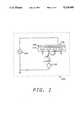
- FIG. 1shows a schematic diagram of the invention
- FIG. 2shows a top cutaway view of an integrated circuit
- FIG. 3shows a side cutaway view of an integrated circuit and illustrates, along with FIG. 2, how the capacitive coupling occurs;
- FIG. 4shows an integrated circuit and associated printed circuit traces, and illustrates shunt current
- FIG. 5shows the invention being used to test a plurality of integrated circuits on a printed circuit board.
- FIG. 1shows a schematic diagram of the invention.
- the system of the present invention 102uses an oscillator 104 which supplies an alternating current signal, typically one megaHertz (1 MHz) at ten (10) volts.
- the output of the oscillator 104is connected to a metallic electrode 106 which is placed on top of an integrated circuit package 110.
- An insulator 108may be placed between the electrode 106 and the integrated circuit package 110.
- a pin under test 112is connected to an integrated circuit trace 114 which is connected to a current measuring device, such as an ammeter, 116.
- the connection to the ammeter 116is typically made through a bed of nails connecting device.
- the oscillator 104When the test is performed, the oscillator 104 is activated and a current is conducted to the electrode 106. Through capacitive coupling, the current is passed to the pin 112 of the integrated circuit 110. The current 112 then passes through a connection to a printed circuit board trace 114 and the current then passes to the ammeter 116 which measures the amount of current. If a threshold amount of current is measured by the ammeter 116, then the pin 112 must be connected to the integrated circuit trace 114 at location 118. If the pin 112 is not connected at location 118, no current will be conducted to the integrated circuit trace 114 and no current will be measured by the ammeter 116 indicating that a pin open fault is present.
- FIG. 2shows a top cut away view of the integrated circuit 110 and the electrode 106
- FIG. 3shows a side cut away view of the integrated circuit 110 and the electrode 106
- FIGS. 2 and 3illustrated how the capacitive coupling occurs between the electrode and the pins of the integrated circuit.
- the integrated circuit package 110contains an integrated circuit 202.
- the integrated circuit 202contains connections, however, which must be made to the outside of the integrated circuit package 110. Therefore, the pin 112 is connected to an internal conductor 204 which connects the pin 112 to a location just adjacent the integrated circuit 202. There a small wire spans between the conductor 204 and a location on the integrated circuit 202. Similar connections are made to all the other pins of the integrated circuit package 110.
- the conductor 204forms a metallic plate, which acts as one plate of a capacitor.
- the other plate of the capacitoris the electrode 106, here illustrated by dashed lines, indicating that the conductor 106 is placed over the top of the integrated circuit package 110.
- the capacitor created in this manneris small, it is sufficient to conduct a signal from the electrode 106 to the pin 112.
- FIG. 4shows an integrated circuit package and associated printed circuit traces that connect the leads to other circuits.
- an integrated circuit package 402contains a pin 404 which is to be tested using the system of the present invention.
- the pin 404is connected to a printed circuit wiring trace 408 which connects it to other integrated circuits on the printed circuit board.
- An electrode 420here illustrated by dashed lines, is placed over the integrated circuit package 402 and connected to an oscillator (not shown in FIG. 4), as described above with respect to FIG. 1.
- the bed of nails tester(not shown) connects to the printed circuit 408 at 418 and also connects to an ammeter (not shown) which will measure the current from tune pin 404.
- the oscillatorWhen the oscillator is activated, the signal from electrode 420 is conducted to pin 404 and if a soldered connection has been made, where pin 404 contacts the printed circuit board, the current from pin 404 will flow through the printed circuit 408 and out to the ammeter (not shown) through the connection at 418.
- the electrode 420covers the entire integrated circuit package 402, current will also be conducted to the other seven pins of the integrated circuit package 402. Through the same process that current is conducted to pin 404, current is also conducted to pin 424 and pin 422, etc.
- the current that flows to pin 424flows through printed circuit wiring trace 406. Because the printed circuit wiring trace 406 and the printed circuit wiring trace 408 run parallel to each other on the printed circuit board, the wiring traces form plates of a small capacitor, here illustrated by the capacitor 412 formed with dashed lines. This capacitor will conduct some of the current flowing through in printed circuit wiring trace 406 to the printed circuit wiring trace 408. Likewise, current flowing from pin 422 into printed circuit trace 410 will be conducted to the printed circuit wiring trace 408 through capacitors 414 and 416. Therefore, the current being measured at location 418 is the sum of the current flowing through pin 404 and current flowing through pins 424 and 422 after the current passes through the capacitors 412, 414 and 416.
- capacitors 412, 414 and 416The current that flows through capacitors 412, 414 and 416 is called shunt current, and comprises about twenty (20%) to fifty percent (50%) of the current that will flow through connection 418. Note that capacitors 412, 414, and 416 are not components on the printed circuit board, but instead are formed by the printed circuit wiring traces running in parallel.
- the ammetermust detect a certain threshold amount of current before the pin under test is considered connected. Although typically the shunt current is approximately twenty percent (20%) of the total current, it could be higher. This shunt current can be reduced by grounding all the printed circuit wiring traces that are not being used in the test. Also, the power input and ground pins of the integrated circuit being tested can be grounded to decrease the amount of shunt current.
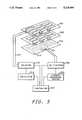
- FIG. 5shows a diagram of the invention when used to test an entire printed circuit board.
- a printed circuit board 500contains a plurality of integrated circuits 506, 508, 510, etc.
- a board 501which contains a plurality of electrodes 502, 503, 504, etc., is placed over the top of the printed circuit board 500.
- a bed of nails tester 513containing a plurality of probe pins 512, 514, etc., is brought into contact with the bottom of the printed circuit board 500 to connect to the printed circuit wiring traces on the printed circuit board 500.
- An oscillator 518supplies a current to a selector 516.
- the selector 516has a plurality of outputs, one for each of the metallic electrodes on the board 501.
- a cable 517containing wires to connect to all the electrodes, connects the output of the selector to the board 501.
- a multiplexor 520contains a series of inputs, one for each of the pins on the bed of nails tester 513. The output of the multiplexor is connected to a current measuring device 522.
- a controller 524is connected to the oscillator 518, the selector 516, the multiplexor 520, and the current measuring device 522.
- the controllerTo test all the integrated circuits on the printed circuit board 500, the controller first selects one of the electrodes on the board 501 by programming the selector 516. The controller then activates the oscillator 518 to supply a current through the selector 516 to the electrode on the board 501 which is directly over the top of the integrated circuit being tested. The controller 524 then selects one of the pins from the bed of nails tester 513 by programming the multiplexor 520. The pin selected will be the pin that connects to a printed circuit board trace on the printed circuit board 500 which is connected to the particular pin of the particular integrated circuit being tested. After the multiplexor is programmed to select the correct pin, the controller activates the current measuring device 522 to determine whether the proper amount of current is present on the printed circuit board trace on the board 500.
- the correct amount of currentis determined, as described above with respect to FIG. 4, by first determining the amount of shunt current (using a fully functional board in a separate test) that will be capacitively coupled to the trace and then determining whether the current measured exceeds the shunt current.
- This processis then repeated for each pin of each integrated circuit on the board. It is important to note that this process is independent of the integrated circuit family, and easily tests TTL, CMOS, etc., and can test multiple families on the same printed circuit board.
Landscapes
- Physics & Mathematics (AREA)
- General Physics & Mathematics (AREA)
- Engineering & Computer Science (AREA)
- General Engineering & Computer Science (AREA)
- Testing Of Short-Circuits, Discontinuities, Leakage, Or Incorrect Line Connections (AREA)
- Tests Of Electronic Circuits (AREA)
Abstract
Description
Claims (11)
Priority Applications (7)
| Application Number | Priority Date | Filing Date | Title |
|---|---|---|---|
| US07/631,609US5124660A (en) | 1990-12-20 | 1990-12-20 | Identification of pin-open faults by capacitive coupling through the integrated circuit package |
| DE69128189TDE69128189T2 (en) | 1990-12-20 | 1991-11-26 | Identification of non-connected pins by capacitive coupling through the housing of the integrated circuit |
| EP91310861AEP0492806B1 (en) | 1990-12-20 | 1991-11-26 | Identification of pin-open faults by capacitive coupling through the integrated circuit package |
| JP35492191AJP3228982B2 (en) | 1990-12-20 | 1991-12-20 | In-circuit test equipment |
| US07/892,868US5254953A (en) | 1990-12-20 | 1992-06-03 | Identification of pin-open faults by capacitive coupling through the integrated circuit package |
| US08/139,362US5625292A (en) | 1990-12-20 | 1993-10-19 | System for measuring the integrity of an electrical contact |
| US08/400,787US5557209A (en) | 1990-12-20 | 1995-03-07 | Identification of pin-open faults by capacitive coupling through the integrated circuit package |
Applications Claiming Priority (1)
| Application Number | Priority Date | Filing Date | Title |
|---|---|---|---|
| US07/631,609US5124660A (en) | 1990-12-20 | 1990-12-20 | Identification of pin-open faults by capacitive coupling through the integrated circuit package |
Related Child Applications (1)
| Application Number | Title | Priority Date | Filing Date |
|---|---|---|---|
| US07/892,868Continuation-In-PartUS5254953A (en) | 1990-12-20 | 1992-06-03 | Identification of pin-open faults by capacitive coupling through the integrated circuit package |
Publications (1)
| Publication Number | Publication Date |
|---|---|
| US5124660Atrue US5124660A (en) | 1992-06-23 |
Family
ID=24531971
Family Applications (1)
| Application Number | Title | Priority Date | Filing Date |
|---|---|---|---|
| US07/631,609Expired - LifetimeUS5124660A (en) | 1990-12-20 | 1990-12-20 | Identification of pin-open faults by capacitive coupling through the integrated circuit package |
Country Status (4)
| Country | Link |
|---|---|
| US (1) | US5124660A (en) |
| EP (1) | EP0492806B1 (en) |
| JP (1) | JP3228982B2 (en) |
| DE (1) | DE69128189T2 (en) |
Cited By (62)
| Publication number | Priority date | Publication date | Assignee | Title |
|---|---|---|---|---|
| US5254953A (en)* | 1990-12-20 | 1993-10-19 | Hewlett-Packard Company | Identification of pin-open faults by capacitive coupling through the integrated circuit package |
| US5268645A (en)* | 1991-04-10 | 1993-12-07 | Atg Electronic Gmbh | Method of and apparatus for testing circuit boards and the like with an inhomogeneous electric field |
| EP0560484A3 (en)* | 1992-03-10 | 1994-06-08 | Hewlett Packard Co | Identification of pin-open faults by capacitive coupling |
| US5391993A (en)* | 1994-01-27 | 1995-02-21 | Genrad, Inc. | Capacitive open-circuit test employing threshold determination |
| DE4417580A1 (en)* | 1993-09-15 | 1995-03-16 | Hewlett Packard Co | Testing electronic assemblies using rotor technology to assemble the sensors |
| US5404110A (en)* | 1993-03-25 | 1995-04-04 | International Business Machines Corporation | System using induced current for contactless testing of wiring networks |
| US5420500A (en)* | 1992-11-25 | 1995-05-30 | Hewlett-Packard Company | Pacitive electrode system for detecting open solder joints in printed circuit assemblies |
| US5424633A (en)* | 1991-01-22 | 1995-06-13 | Advanced Test Technologies Inc. | Contactless test method and system for testing printed circuit boards |
| US5426372A (en)* | 1993-07-30 | 1995-06-20 | Genrad, Inc. | Probe for capacitive open-circuit tests |
| US5459738A (en)* | 1994-01-26 | 1995-10-17 | Watari; Hiromichi | Apparatus and method for digital circuit testing |
| US5489851A (en)* | 1992-08-06 | 1996-02-06 | Hewlett-Packard Company | Identification of pin-open faults by measuring current or voltage change resulting from temperature change |
| US5517110A (en)* | 1995-04-06 | 1996-05-14 | Yentec Inc. | Contactless test method and system for testing printed circuit boards |
| US5554928A (en)* | 1994-10-25 | 1996-09-10 | Teradyne, Inc. | Manufacturing defect analyzer |
| US5557209A (en)* | 1990-12-20 | 1996-09-17 | Hewlett-Packard Company | Identification of pin-open faults by capacitive coupling through the integrated circuit package |
| US5578930A (en)* | 1995-03-16 | 1996-11-26 | Teradyne, Inc. | Manufacturing defect analyzer with improved fault coverage |
| US5625292A (en)* | 1990-12-20 | 1997-04-29 | Hewlett-Packard Company | System for measuring the integrity of an electrical contact |
| US5631572A (en)* | 1993-09-17 | 1997-05-20 | Teradyne, Inc. | Printed circuit board tester using magnetic induction |
| US5639390A (en)* | 1993-12-24 | 1997-06-17 | Tokyo Electron Limited | Conductor pattern check apparatus for locating and repairing open circuits |
| US5680057A (en)* | 1994-01-06 | 1997-10-21 | Hewlett-Packard Company | Integrated circuit testing assembly and method |
| US5694053A (en)* | 1995-06-07 | 1997-12-02 | Xerox Corporation | Display matrix tester |
| US5712570A (en)* | 1994-09-27 | 1998-01-27 | Anam Industrial Co., Ltd. | Method for checking a wire bond of a semiconductor package |
| US5811980A (en)* | 1995-08-21 | 1998-09-22 | Genrad, Inc. | Test system for determining the orientation of components on a circuit board |
| US5818246A (en)* | 1996-05-07 | 1998-10-06 | Zhong; George Guozhen | Automatic multi-probe PWB tester |
| WO1998053382A3 (en)* | 1997-05-20 | 1999-03-25 | Hayes Microcomputer Prod | Testing the integrity of an electrical connection to a device using an onboard controllable signal source |
| WO1999064879A1 (en)* | 1998-06-09 | 1999-12-16 | Zen Licensing Group, Llp | A method and apparatus for finding and locating manufacturing defects on a printed circuit board |
| US6087842A (en)* | 1996-04-29 | 2000-07-11 | Agilent Technologies | Integrated or intrapackage capability for testing electrical continuity between an integrated circuit and other circuitry |
| US6124715A (en)* | 1998-04-13 | 2000-09-26 | Lucent Technologies, Inc. | Testing of live circuit boards |
| US6181152B1 (en)* | 1997-11-18 | 2001-01-30 | Stmicroelectronics S.A. | Method and system for testing an integrated circuit input capacitance, particularly for a contactless operating integrated circuit |
| US6188235B1 (en)* | 1993-06-15 | 2001-02-13 | Scorpion Technologies Ag | System and method for verifying proper connection of an integrated circuit to a circuit board |
| US6201398B1 (en) | 1996-03-28 | 2001-03-13 | Oht Inc. | Non-contact board inspection probe |
| US6201403B1 (en)* | 1997-09-22 | 2001-03-13 | Nortel Networks Limited | Integrated circuit package shielding characterization method and apparatus |
| US6268719B1 (en)* | 1998-09-23 | 2001-07-31 | Delaware Capital Formation, Inc. | Printed circuit board test apparatus |
| US20020163342A1 (en)* | 2000-06-16 | 2002-11-07 | Shogo Ishioka | Device and method for inspection |
| US6496013B1 (en)* | 1997-09-24 | 2002-12-17 | Scorpion Technologies Ag | Device for testing circuit boards |
| US6529019B1 (en) | 2000-10-23 | 2003-03-04 | Agilent Technologies, Inc. | Multiple axis magnetic test for open integrated circuit pins |
| US6600325B2 (en)* | 2001-02-06 | 2003-07-29 | Sun Microsystems, Inc. | Method and apparatus for probing an integrated circuit through capacitive coupling |
| US6710607B2 (en)* | 2000-03-24 | 2004-03-23 | Oht, Inc. | Method and apparatus for inspection |
| US20040075067A1 (en)* | 2002-10-16 | 2004-04-22 | Mcauliffe Robert E. | Method for detecting missing components at electrical board test using optoelectronic fixture-mounted sensors |
| US6734681B2 (en) | 2001-08-10 | 2004-05-11 | James Sabey | Apparatus and methods for testing circuit boards |
| US6788078B2 (en) | 2001-11-16 | 2004-09-07 | Delaware Capital Formation, Inc. | Apparatus for scan testing printed circuit boards |
| US20040235265A1 (en)* | 2003-05-20 | 2004-11-25 | Philip Neaves | System and method for balancing capacitively coupled signal lines |
| US20050040839A1 (en)* | 2003-08-21 | 2005-02-24 | Philip Neaves | System and method for testing devices utilizing capacitively coupled signaling |
| US20050077546A1 (en)* | 2003-10-13 | 2005-04-14 | Philip Neaves | Structure and method for forming a capacitively coupled chip-to-chip signaling interface |
| US20070001686A1 (en)* | 2005-06-29 | 2007-01-04 | Parker Kenneth P | Methods and apparatus for non-contact testing and diagnosing of open connections on non-probed nodes |
| US20070001687A1 (en)* | 2005-06-29 | 2007-01-04 | Schneider Myron J | Method for using internal semiconductor junctions to aid in non-contact testing |
| US20070013383A1 (en)* | 2005-07-12 | 2007-01-18 | Parker Kenneth P | Methods and apparatus for unpowered testing of open connections on power and ground nodes of circuit devices |
| US20070018672A1 (en)* | 2005-07-23 | 2007-01-25 | Jacobsen Chris R | Method and apparatus for engineering a testability interposer for testing sockets and connectors on printed circuit boards |
| US7224169B2 (en) | 2004-11-02 | 2007-05-29 | Agilent Technologies, Inc. | Methods and apparatus for non-contact testing and diagnosing of inaccessible shorted connections |
| US20070152688A1 (en)* | 2005-12-29 | 2007-07-05 | Samsung Electronics Co., Ltd. | Probe card capable of multi-probing |
| US7295031B1 (en) | 2006-07-12 | 2007-11-13 | Agilent Technologies, Inc. | Method for non-contact testing of marginal integrated circuit connections |
| US20100090679A1 (en)* | 2008-10-15 | 2010-04-15 | Test Research, Inc | Apparatus for testing printed circuit and method therefor |
| US20110148446A1 (en)* | 2009-12-22 | 2011-06-23 | Suto Anthony J | Capacitive opens testing in low signal environments |
| US20110148450A1 (en)* | 2009-12-22 | 2011-06-23 | Suto Anthony J | Low capacitance probe for testing circuit assembly |
| US20110156718A1 (en)* | 2009-12-31 | 2011-06-30 | Su-Wei Tsai | Electrical connection defect detection device |
| US20110156717A1 (en)* | 2009-12-31 | 2011-06-30 | Su-Wei Tsai | Electrical connection defect detection system and method |
| US20110210759A1 (en)* | 2008-11-14 | 2011-09-01 | Teradyne, Inc | Fast open circuit detection for open power and ground pins |
| US20120326698A1 (en)* | 2010-03-25 | 2012-12-27 | Yazaki Corporation | Joint connector and method for identifying bus bar pattern in joint connector |
| WO2013124711A1 (en)* | 2012-02-24 | 2013-08-29 | Freescale Semiconductor, Inc. | A semiconductor device comprising an output driver circuitry, a packaged semiconductor device and associated methods |
| US20140300381A1 (en)* | 2007-08-03 | 2014-10-09 | Rosenberger Hochfrequenztechnik Gmbh & Co. Kg | Contactless measuring system |
| CN104569727A (en)* | 2015-01-23 | 2015-04-29 | 珠海隆芯电子科技有限公司 | Non-contact electronic circuit testing device and testing method |
| TWI512308B (en)* | 2013-04-09 | 2015-12-11 | Nidec Read Corp | Inspecting method and inspecting apparatus |
| US10942225B2 (en)* | 2018-07-10 | 2021-03-09 | Kabushiki Kaisha Toshiba | Wiring open detection circuit |
Families Citing this family (5)
| Publication number | Priority date | Publication date | Assignee | Title |
|---|---|---|---|---|
| IT1261074B (en)* | 1993-07-05 | 1996-05-08 | Luciano Bonaria | METHOD AND TESTING DEVICE FOR ELECTRONIC BOARDS |
| JP3006431U (en)* | 1994-07-04 | 1995-01-24 | 有限会社チェック電子 | Inspection device for liquid crystal display substrate by non-connection signal detection plate |
| GB2353399A (en)* | 1999-08-20 | 2001-02-21 | 3Com Corp | Testing printed or integrated circuits |
| EP2131204B1 (en) | 2008-06-06 | 2012-11-14 | Texas Instruments France | A method and system for testing a semiconductor package |
| JP2013181567A (en) | 2012-02-29 | 2013-09-12 | Honda Motor Co Ltd | Balancer shaft |
Citations (6)
| Publication number | Priority date | Publication date | Assignee | Title |
|---|---|---|---|---|
| US4056773A (en)* | 1976-08-25 | 1977-11-01 | Sullivan Donald F | Printed circuit board open circuit tester |
| US4186338A (en)* | 1976-12-16 | 1980-01-29 | Genrad, Inc. | Phase change detection method of and apparatus for current-tracing the location of faults on printed circuit boards and similar systems |
| GB2143954A (en)* | 1983-07-22 | 1985-02-20 | Sharetree Ltd | A capacitive method and apparatus for checking connections of a printed circuit board |
| US4779041A (en)* | 1987-05-20 | 1988-10-18 | Hewlett-Packard Company | Integrated circuit transfer test device system |
| US4789829A (en)* | 1986-07-18 | 1988-12-06 | Science Application International Corporation | Method and apparatus for determining RE gasket shielding effectiveness |
| US5006808A (en)* | 1989-03-21 | 1991-04-09 | Bath Scientific Limited | Testing electrical circuits |
Family Cites Families (4)
| Publication number | Priority date | Publication date | Assignee | Title |
|---|---|---|---|---|
| US4055801A (en)* | 1970-08-18 | 1977-10-25 | Pike Harold L | Automatic electronic test equipment and method |
| US4695788A (en)* | 1984-12-11 | 1987-09-22 | Hughes Aircraft Company | Open fault location system for photovoltaic module strings |
| GB8521139D0 (en)* | 1985-08-23 | 1985-10-02 | Bicc Plc | Terminating electrical connectors |
| FR2623615B1 (en) | 1987-11-20 | 1991-01-25 | Thomson Csf | ELECTRONIC MEASUREMENT OF A SURFACE, ESPECIALLY APPLICABLE TO CONNECTION CONTROL |
- 1990
- 1990-12-20USUS07/631,609patent/US5124660A/ennot_activeExpired - Lifetime
- 1991
- 1991-11-26DEDE69128189Tpatent/DE69128189T2/ennot_activeExpired - Fee Related
- 1991-11-26EPEP91310861Apatent/EP0492806B1/ennot_activeExpired - Lifetime
- 1991-12-20JPJP35492191Apatent/JP3228982B2/ennot_activeExpired - Fee Related
Patent Citations (6)
| Publication number | Priority date | Publication date | Assignee | Title |
|---|---|---|---|---|
| US4056773A (en)* | 1976-08-25 | 1977-11-01 | Sullivan Donald F | Printed circuit board open circuit tester |
| US4186338A (en)* | 1976-12-16 | 1980-01-29 | Genrad, Inc. | Phase change detection method of and apparatus for current-tracing the location of faults on printed circuit boards and similar systems |
| GB2143954A (en)* | 1983-07-22 | 1985-02-20 | Sharetree Ltd | A capacitive method and apparatus for checking connections of a printed circuit board |
| US4789829A (en)* | 1986-07-18 | 1988-12-06 | Science Application International Corporation | Method and apparatus for determining RE gasket shielding effectiveness |
| US4779041A (en)* | 1987-05-20 | 1988-10-18 | Hewlett-Packard Company | Integrated circuit transfer test device system |
| US5006808A (en)* | 1989-03-21 | 1991-04-09 | Bath Scientific Limited | Testing electrical circuits |
Cited By (109)
| Publication number | Priority date | Publication date | Assignee | Title |
|---|---|---|---|---|
| US5254953A (en)* | 1990-12-20 | 1993-10-19 | Hewlett-Packard Company | Identification of pin-open faults by capacitive coupling through the integrated circuit package |
| US5625292A (en)* | 1990-12-20 | 1997-04-29 | Hewlett-Packard Company | System for measuring the integrity of an electrical contact |
| US5557209A (en)* | 1990-12-20 | 1996-09-17 | Hewlett-Packard Company | Identification of pin-open faults by capacitive coupling through the integrated circuit package |
| US5424633A (en)* | 1991-01-22 | 1995-06-13 | Advanced Test Technologies Inc. | Contactless test method and system for testing printed circuit boards |
| US5268645A (en)* | 1991-04-10 | 1993-12-07 | Atg Electronic Gmbh | Method of and apparatus for testing circuit boards and the like with an inhomogeneous electric field |
| US5469064A (en)* | 1992-01-14 | 1995-11-21 | Hewlett-Packard Company | Electrical assembly testing using robotic positioning of probes |
| EP0560484A3 (en)* | 1992-03-10 | 1994-06-08 | Hewlett Packard Co | Identification of pin-open faults by capacitive coupling |
| US5696451A (en)* | 1992-03-10 | 1997-12-09 | Hewlett-Packard Co. | Identification of pin-open faults by capacitive coupling |
| EP0573159A3 (en)* | 1992-06-03 | 1994-05-11 | Hewlett Packard Co | Identification of pin-open faults by capacitive coupling through the integrated circuit package |
| US5489851A (en)* | 1992-08-06 | 1996-02-06 | Hewlett-Packard Company | Identification of pin-open faults by measuring current or voltage change resulting from temperature change |
| US5420500A (en)* | 1992-11-25 | 1995-05-30 | Hewlett-Packard Company | Pacitive electrode system for detecting open solder joints in printed circuit assemblies |
| US5404110A (en)* | 1993-03-25 | 1995-04-04 | International Business Machines Corporation | System using induced current for contactless testing of wiring networks |
| US5612626A (en)* | 1993-03-25 | 1997-03-18 | International Business Machines Corporation | System using induced current for contactless testing of wiring networks |
| US6188235B1 (en)* | 1993-06-15 | 2001-02-13 | Scorpion Technologies Ag | System and method for verifying proper connection of an integrated circuit to a circuit board |
| US5426372A (en)* | 1993-07-30 | 1995-06-20 | Genrad, Inc. | Probe for capacitive open-circuit tests |
| DE4417580A1 (en)* | 1993-09-15 | 1995-03-16 | Hewlett Packard Co | Testing electronic assemblies using rotor technology to assemble the sensors |
| US5631572A (en)* | 1993-09-17 | 1997-05-20 | Teradyne, Inc. | Printed circuit board tester using magnetic induction |
| US5844199A (en)* | 1993-12-24 | 1998-12-01 | Tokyo Electron Ltd | Conductor pattern check apparatus for locating and repairing short and open circuits |
| US5639390A (en)* | 1993-12-24 | 1997-06-17 | Tokyo Electron Limited | Conductor pattern check apparatus for locating and repairing open circuits |
| US5680057A (en)* | 1994-01-06 | 1997-10-21 | Hewlett-Packard Company | Integrated circuit testing assembly and method |
| US5459738A (en)* | 1994-01-26 | 1995-10-17 | Watari; Hiromichi | Apparatus and method for digital circuit testing |
| US5786697A (en)* | 1994-01-27 | 1998-07-28 | Genrad, Inc. | Capacitive open-circuit and short-circuit tests of component connections to circuit boards |
| US5391993A (en)* | 1994-01-27 | 1995-02-21 | Genrad, Inc. | Capacitive open-circuit test employing threshold determination |
| US5712570A (en)* | 1994-09-27 | 1998-01-27 | Anam Industrial Co., Ltd. | Method for checking a wire bond of a semiconductor package |
| US5554928A (en)* | 1994-10-25 | 1996-09-10 | Teradyne, Inc. | Manufacturing defect analyzer |
| US5578930A (en)* | 1995-03-16 | 1996-11-26 | Teradyne, Inc. | Manufacturing defect analyzer with improved fault coverage |
| US5517110A (en)* | 1995-04-06 | 1996-05-14 | Yentec Inc. | Contactless test method and system for testing printed circuit boards |
| US5694053A (en)* | 1995-06-07 | 1997-12-02 | Xerox Corporation | Display matrix tester |
| US5811980A (en)* | 1995-08-21 | 1998-09-22 | Genrad, Inc. | Test system for determining the orientation of components on a circuit board |
| US6373258B2 (en) | 1996-03-28 | 2002-04-16 | Naoya Takada | Non-contact board inspection probe |
| US6201398B1 (en) | 1996-03-28 | 2001-03-13 | Oht Inc. | Non-contact board inspection probe |
| US6087842A (en)* | 1996-04-29 | 2000-07-11 | Agilent Technologies | Integrated or intrapackage capability for testing electrical continuity between an integrated circuit and other circuitry |
| US6097203A (en)* | 1996-04-29 | 2000-08-01 | Agilent Technologies | Integrated or intrapackage capability for testing electrical continuity between an integrated circuit and other circuitry |
| US5818246A (en)* | 1996-05-07 | 1998-10-06 | Zhong; George Guozhen | Automatic multi-probe PWB tester |
| US6104198A (en)* | 1997-05-20 | 2000-08-15 | Zen Licensing Group Llp | Testing the integrity of an electrical connection to a device using an onboard controllable signal source |
| WO1998053382A3 (en)* | 1997-05-20 | 1999-03-25 | Hayes Microcomputer Prod | Testing the integrity of an electrical connection to a device using an onboard controllable signal source |
| US6201403B1 (en)* | 1997-09-22 | 2001-03-13 | Nortel Networks Limited | Integrated circuit package shielding characterization method and apparatus |
| US6496013B1 (en)* | 1997-09-24 | 2002-12-17 | Scorpion Technologies Ag | Device for testing circuit boards |
| US6181152B1 (en)* | 1997-11-18 | 2001-01-30 | Stmicroelectronics S.A. | Method and system for testing an integrated circuit input capacitance, particularly for a contactless operating integrated circuit |
| US6124715A (en)* | 1998-04-13 | 2000-09-26 | Lucent Technologies, Inc. | Testing of live circuit boards |
| US6144210A (en)* | 1998-06-09 | 2000-11-07 | Zen Licensing Group, Llp | Method and apparatus for finding and locating manufacturing defects on a printed circuit board |
| WO1999064879A1 (en)* | 1998-06-09 | 1999-12-16 | Zen Licensing Group, Llp | A method and apparatus for finding and locating manufacturing defects on a printed circuit board |
| US6268719B1 (en)* | 1998-09-23 | 2001-07-31 | Delaware Capital Formation, Inc. | Printed circuit board test apparatus |
| US6710607B2 (en)* | 2000-03-24 | 2004-03-23 | Oht, Inc. | Method and apparatus for inspection |
| US7138805B2 (en)* | 2000-06-16 | 2006-11-21 | Oht, Inc. | Device and method for inspection |
| US20020163342A1 (en)* | 2000-06-16 | 2002-11-07 | Shogo Ishioka | Device and method for inspection |
| US6529019B1 (en) | 2000-10-23 | 2003-03-04 | Agilent Technologies, Inc. | Multiple axis magnetic test for open integrated circuit pins |
| US6600325B2 (en)* | 2001-02-06 | 2003-07-29 | Sun Microsystems, Inc. | Method and apparatus for probing an integrated circuit through capacitive coupling |
| US6734681B2 (en) | 2001-08-10 | 2004-05-11 | James Sabey | Apparatus and methods for testing circuit boards |
| US6788078B2 (en) | 2001-11-16 | 2004-09-07 | Delaware Capital Formation, Inc. | Apparatus for scan testing printed circuit boards |
| US7071716B2 (en) | 2001-11-16 | 2006-07-04 | Delaware Capital Formation, Inc. | Apparatus for scan testing printed circuit boards |
| US20050001640A1 (en)* | 2001-11-16 | 2005-01-06 | Delaware Capital Formation, Inc. | Apparatus for scan testing printed circuit boards |
| US20040075067A1 (en)* | 2002-10-16 | 2004-04-22 | Mcauliffe Robert E. | Method for detecting missing components at electrical board test using optoelectronic fixture-mounted sensors |
| SG129257A1 (en)* | 2002-10-16 | 2007-02-26 | Agilent Technologies Inc | A method for detecting missing components at electrical board test using optoelectronic fixture-mounted sensors |
| US6903360B2 (en)* | 2002-10-16 | 2005-06-07 | Agilent Technologies, Inc. | Method for detecting missing components at electrical board test using optoelectronic fixture-mounted sensors |
| US6937067B2 (en) | 2003-05-20 | 2005-08-30 | Micron Technology, Inc. | System and method for balancing capacitively coupled signal lines |
| US7075330B2 (en) | 2003-05-20 | 2006-07-11 | Micron Technology, Inc. | System and method for balancing capacitively coupled signal lines |
| US20050280444A1 (en)* | 2003-05-20 | 2005-12-22 | Philip Neaves | System and method for balancing capacitively coupled signal lines |
| US20040235265A1 (en)* | 2003-05-20 | 2004-11-25 | Philip Neaves | System and method for balancing capacitively coupled signal lines |
| US20050206403A1 (en)* | 2003-08-21 | 2005-09-22 | Philip Neaves | System and method for testing devices utilizing capacitively coupled signaling |
| US7274204B2 (en) | 2003-08-21 | 2007-09-25 | Micron Technology, Inc. | System and method for testing devices utilizing capacitively coupled signaling |
| US20060152243A1 (en)* | 2003-08-21 | 2006-07-13 | Philip Neaves | System and method for testing devices utilizing capacitively coupled signaling |
| US20060170446A1 (en)* | 2003-08-21 | 2006-08-03 | Philip Neaves | System and method for testing devices utilizing capacitively coupled signaling |
| US20060181301A1 (en)* | 2003-08-21 | 2006-08-17 | Philip Neaves | System and method for testing devices utilizing capacitively coupled signaling |
| US7112980B2 (en)* | 2003-08-21 | 2006-09-26 | Micron Technology, Inc. | System and method for testing devices utilizing capacitively coupled signaling |
| US20050040839A1 (en)* | 2003-08-21 | 2005-02-24 | Philip Neaves | System and method for testing devices utilizing capacitively coupled signaling |
| US7352201B2 (en)* | 2003-08-21 | 2008-04-01 | Micron Technology, Inc. | System and method for testing devices utilizing capacitively coupled signaling |
| US7276928B2 (en)* | 2003-08-21 | 2007-10-02 | Micron Technology, Inc. | System and method for testing devices utilizing capacitively coupled signaling |
| US20060152244A1 (en)* | 2003-08-21 | 2006-07-13 | School Juridical Person, Kinki University | System and method for testing devices utilizing capacitively coupled signaling |
| US7274205B2 (en)* | 2003-08-21 | 2007-09-25 | Micron Technology, Inc. | System and method for testing devices utilizing capacitively coupled signaling |
| US7183790B2 (en)* | 2003-08-21 | 2007-02-27 | Micron Technology, Inc. | System and method for testing devices utilizing capacitively coupled signaling |
| US20050077546A1 (en)* | 2003-10-13 | 2005-04-14 | Philip Neaves | Structure and method for forming a capacitively coupled chip-to-chip signaling interface |
| US20100283158A1 (en)* | 2003-10-13 | 2010-11-11 | Micron Technology, Inc. | Structure and method for forming a capacitively coupled chip-to-chip signaling interface |
| US8049331B2 (en) | 2003-10-13 | 2011-11-01 | Micron Technology, Inc. | Structure and method for forming a capacitively coupled chip-to-chip signaling interface |
| US7462935B2 (en) | 2003-10-13 | 2008-12-09 | Micron Technology, Inc. | Structure and method for forming a capacitively coupled chip-to-chip signaling interface |
| US7763497B2 (en) | 2003-10-13 | 2010-07-27 | Micron Technology, Inc. | Structure and method for forming a capacitively coupled chip-to-chip signaling interface |
| US20090072389A1 (en)* | 2003-10-13 | 2009-03-19 | Micron Technology, Inc. | Structure and method for forming a capacitively coupled chip-to-chip signaling interface |
| US7224169B2 (en) | 2004-11-02 | 2007-05-29 | Agilent Technologies, Inc. | Methods and apparatus for non-contact testing and diagnosing of inaccessible shorted connections |
| US20070001687A1 (en)* | 2005-06-29 | 2007-01-04 | Schneider Myron J | Method for using internal semiconductor junctions to aid in non-contact testing |
| US7327148B2 (en) | 2005-06-29 | 2008-02-05 | Agilent Technologies, Inc. | Method for using internal semiconductor junctions to aid in non-contact testing |
| US20070001686A1 (en)* | 2005-06-29 | 2007-01-04 | Parker Kenneth P | Methods and apparatus for non-contact testing and diagnosing of open connections on non-probed nodes |
| US7362106B2 (en) | 2005-06-29 | 2008-04-22 | Agilent Technologies, Inc. | Methods and apparatus for non-contact testing and diagnosing of open connections on non-probed nodes |
| US20070013383A1 (en)* | 2005-07-12 | 2007-01-18 | Parker Kenneth P | Methods and apparatus for unpowered testing of open connections on power and ground nodes of circuit devices |
| US7307427B2 (en) | 2005-07-23 | 2007-12-11 | Agilent Technologies, Inc. | Method and apparatus for engineering a testability interposer for testing sockets and connectors on printed circuit boards |
| US20070018672A1 (en)* | 2005-07-23 | 2007-01-25 | Jacobsen Chris R | Method and apparatus for engineering a testability interposer for testing sockets and connectors on printed circuit boards |
| US7659735B2 (en)* | 2005-12-29 | 2010-02-09 | Min-Gu Kim | Probe card capable of multi-probing |
| US20070152688A1 (en)* | 2005-12-29 | 2007-07-05 | Samsung Electronics Co., Ltd. | Probe card capable of multi-probing |
| US7295031B1 (en) | 2006-07-12 | 2007-11-13 | Agilent Technologies, Inc. | Method for non-contact testing of marginal integrated circuit connections |
| US9291644B2 (en)* | 2007-08-03 | 2016-03-22 | Rosenberger Hochfrequenztechnik Gmbh & Co. Kg. | Contactless measuring system for contactless decoupling of a signal running on a signal waveguide |
| US20140300381A1 (en)* | 2007-08-03 | 2014-10-09 | Rosenberger Hochfrequenztechnik Gmbh & Co. Kg | Contactless measuring system |
| US8179143B2 (en) | 2008-10-15 | 2012-05-15 | Test Research, Inc. | Apparatus for testing printed circuit and method therefor |
| US20100090679A1 (en)* | 2008-10-15 | 2010-04-15 | Test Research, Inc | Apparatus for testing printed circuit and method therefor |
| US8760183B2 (en)* | 2008-11-14 | 2014-06-24 | Teradyne, Inc. | Fast open circuit detection for open power and ground pins |
| US20110210759A1 (en)* | 2008-11-14 | 2011-09-01 | Teradyne, Inc | Fast open circuit detection for open power and ground pins |
| US8310256B2 (en) | 2009-12-22 | 2012-11-13 | Teradyne, Inc. | Capacitive opens testing in low signal environments |
| US8760185B2 (en) | 2009-12-22 | 2014-06-24 | Anthony J. Suto | Low capacitance probe for testing circuit assembly |
| US20110148446A1 (en)* | 2009-12-22 | 2011-06-23 | Suto Anthony J | Capacitive opens testing in low signal environments |
| US20110148450A1 (en)* | 2009-12-22 | 2011-06-23 | Suto Anthony J | Low capacitance probe for testing circuit assembly |
| US8350575B2 (en)* | 2009-12-31 | 2013-01-08 | Test Research, Inc. | Electrical connection defect detection system and method |
| US20110156718A1 (en)* | 2009-12-31 | 2011-06-30 | Su-Wei Tsai | Electrical connection defect detection device |
| US20110156717A1 (en)* | 2009-12-31 | 2011-06-30 | Su-Wei Tsai | Electrical connection defect detection system and method |
| US8324908B2 (en)* | 2009-12-31 | 2012-12-04 | Test Research, Inc. | Electrical connection defect detection device |
| US20120326698A1 (en)* | 2010-03-25 | 2012-12-27 | Yazaki Corporation | Joint connector and method for identifying bus bar pattern in joint connector |
| US9214775B2 (en)* | 2010-03-25 | 2015-12-15 | Yazaki Corporation | Joint connector and method for identifying bus bar pattern in joint connector |
| WO2013124711A1 (en)* | 2012-02-24 | 2013-08-29 | Freescale Semiconductor, Inc. | A semiconductor device comprising an output driver circuitry, a packaged semiconductor device and associated methods |
| US9575118B2 (en) | 2012-02-24 | 2017-02-21 | Nxp Usa, Inc. | Semiconductor device comprising an output driver circuitry, a packaged semiconductor device and associated methods |
| TWI512308B (en)* | 2013-04-09 | 2015-12-11 | Nidec Read Corp | Inspecting method and inspecting apparatus |
| CN104569727A (en)* | 2015-01-23 | 2015-04-29 | 珠海隆芯电子科技有限公司 | Non-contact electronic circuit testing device and testing method |
| US10942225B2 (en)* | 2018-07-10 | 2021-03-09 | Kabushiki Kaisha Toshiba | Wiring open detection circuit |
Also Published As
| Publication number | Publication date |
|---|---|
| EP0492806A2 (en) | 1992-07-01 |
| DE69128189T2 (en) | 1998-03-12 |
| EP0492806B1 (en) | 1997-11-12 |
| JP3228982B2 (en) | 2001-11-12 |
| JPH04309875A (en) | 1992-11-02 |
| EP0492806A3 (en) | 1992-10-14 |
| DE69128189D1 (en) | 1997-12-18 |
Similar Documents
| Publication | Publication Date | Title |
|---|---|---|
| US5124660A (en) | Identification of pin-open faults by capacitive coupling through the integrated circuit package | |
| EP0560484B1 (en) | Identification of pin-open faults by capacitive coupling | |
| US5557209A (en) | Identification of pin-open faults by capacitive coupling through the integrated circuit package | |
| US5254953A (en) | Identification of pin-open faults by capacitive coupling through the integrated circuit package | |
| US5420500A (en) | Pacitive electrode system for detecting open solder joints in printed circuit assemblies | |
| JP3784412B2 (en) | Manufacturing defect analyzer with expanded fault coverage | |
| US5631572A (en) | Printed circuit board tester using magnetic induction | |
| US5517110A (en) | Contactless test method and system for testing printed circuit boards | |
| US6930494B2 (en) | Capacitive probe assembly with flex circuit | |
| JPH09264919A (en) | Method and device for inspecting board | |
| JPH01112179A (en) | Circuit board inspection instrument | |
| JPH0682509A (en) | Device and method for testing circuit | |
| US7075307B1 (en) | Method and apparatus for detecting shorts on inaccessible pins using capacitive measurements | |
| KR100476740B1 (en) | Method for testing rlc parallel circuit on the printed circuit board | |
| JP2002131365A (en) | Inspection method and inspection device | |
| US20080088318A1 (en) | Method to test transparent-to-test capacitors | |
| KR20050068118A (en) | Method for testing the needle of probe card | |
| Hashizume et al. | Test Circuit for Open Lead Detection of CMOS ICs Based on Supply Current | |
| KR19990025832A (en) | Inspection substrate with resonant circuit for measuring noise in specific frequency band | |
| JPH05121499A (en) | Circuit connection tester | |
| JPH07140193A (en) | Method and equipment for checking burn-in board |
Legal Events
| Date | Code | Title | Description |
|---|---|---|---|
| AS | Assignment | Owner name:HEWLETT-PACKARD COMPANY, A CORP. OF CA, CALIFORNIA Free format text:ASSIGNMENT OF ASSIGNORS INTEREST.;ASSIGNOR:CILINGIROGLU, UGUR;REEL/FRAME:005602/0862 Effective date:19901213 | |
| STCF | Information on status: patent grant | Free format text:PATENTED CASE | |
| FEPP | Fee payment procedure | Free format text:PAYOR NUMBER ASSIGNED (ORIGINAL EVENT CODE: ASPN); ENTITY STATUS OF PATENT OWNER: LARGE ENTITY | |
| FPAY | Fee payment | Year of fee payment:4 | |
| FPAY | Fee payment | Year of fee payment:8 | |
| AS | Assignment | Owner name:HEWLETT-PACKARD COMPANY, A DELAWARE CORPORATION, C Free format text:MERGER;ASSIGNOR:HEWLETT-PACKARD COMPANY, A CALIFORNIA CORPORATION;REEL/FRAME:010841/0649 Effective date:19980520 | |
| AS | Assignment | Owner name:AGILENT TECHNOLOGIES INC., CALIFORNIA Free format text:ASSIGNMENT OF ASSIGNORS INTEREST;ASSIGNOR:HEWLETT-PACKARD COMPANY, A DELAWARE CORPORATION;REEL/FRAME:010901/0336 Effective date:20000520 | |
| AS | Assignment | Owner name:AGILENT TECHNOLOGIES, INC., COLORADO Free format text:ASSIGNMENT OF ASSIGNORS INTEREST;ASSIGNOR:HEWLETT-PACKARD COMPANY, A DELAWARE CORPORATION;REEL/FRAME:012381/0616 Effective date:20011119 | |
| CC | Certificate of correction | ||
| FPAY | Fee payment | Year of fee payment:12 |