US5123848A - Computer signal interconnect apparatus - Google Patents
Computer signal interconnect apparatusDownload PDFInfo
- Publication number
- US5123848A US5123848AUS07/556,024US55602490AUS5123848AUS 5123848 AUS5123848 AUS 5123848AUS 55602490 AUS55602490 AUS 55602490AUS 5123848 AUS5123848 AUS 5123848A
- Authority
- US
- United States
- Prior art keywords
- interconnect
- board
- connector
- middle layer
- holes
- Prior art date
- Legal status (The legal status is an assumption and is not a legal conclusion. Google has not performed a legal analysis and makes no representation as to the accuracy of the status listed.)
- Expired - Lifetime
Links
Images
Classifications
- G—PHYSICS
- G06—COMPUTING OR CALCULATING; COUNTING
- G06F—ELECTRIC DIGITAL DATA PROCESSING
- G06F13/00—Interconnection of, or transfer of information or other signals between, memories, input/output devices or central processing units
- G06F13/38—Information transfer, e.g. on bus
- G06F13/40—Bus structure
- G06F13/4063—Device-to-bus coupling
- G06F13/409—Mechanical coupling
- H—ELECTRICITY
- H01—ELECTRIC ELEMENTS
- H01R—ELECTRICALLY-CONDUCTIVE CONNECTIONS; STRUCTURAL ASSOCIATIONS OF A PLURALITY OF MUTUALLY-INSULATED ELECTRICAL CONNECTING ELEMENTS; COUPLING DEVICES; CURRENT COLLECTORS
- H01R12/00—Structural associations of a plurality of mutually-insulated electrical connecting elements, specially adapted for printed circuits, e.g. printed circuit boards [PCB], flat or ribbon cables, or like generally planar structures, e.g. terminal strips, terminal blocks; Coupling devices specially adapted for printed circuits, flat or ribbon cables, or like generally planar structures; Terminals specially adapted for contact with, or insertion into, printed circuits, flat or ribbon cables, or like generally planar structures
- H01R12/50—Fixed connections
- H01R12/51—Fixed connections for rigid printed circuits or like structures
- H01R12/52—Fixed connections for rigid printed circuits or like structures connecting to other rigid printed circuits or like structures
- H01R12/523—Fixed connections for rigid printed circuits or like structures connecting to other rigid printed circuits or like structures by an interconnection through aligned holes in the boards or multilayer board
- H—ELECTRICITY
- H01—ELECTRIC ELEMENTS
- H01R—ELECTRICALLY-CONDUCTIVE CONNECTIONS; STRUCTURAL ASSOCIATIONS OF A PLURALITY OF MUTUALLY-INSULATED ELECTRICAL CONNECTING ELEMENTS; COUPLING DEVICES; CURRENT COLLECTORS
- H01R13/00—Details of coupling devices of the kinds covered by groups H01R12/70 or H01R24/00 - H01R33/00
- H01R13/02—Contact members
- H01R13/33—Contact members made of resilient wire
Definitions
- This inventionrelates generally to a method and apparatus for electrically interconnecting logic boards in computer systems.
- itis directed to an electrical backplane comprised of an assembly pressure connector and connector interconnect board that electrically connect logic boards to external wiring.
- Electrical backplaneswhich are well known in the art, are designed to provide electrical interconnection for logic boards or assemblies in computer systems. However, as logic board densities increase, it becomes more important to increase the density of interconnections in the electrical backplanes.
- Pressure connectorshave been used in the prior art to make these high density interconnections.
- Pressure connectorshave bumps, usually comprised of solder or gold, on their surfaces.
- the pressure connectoris placed adjacent to the logic board and the bumps on the pressure connector are aligned with the contact points on the logic board so as to make the electrical interconnection when the pressure connector is pressed against the logic board.
- the problem with direct interconnection between pressure connector bumps and logic board contact pointsis that after a period of time the bumps become permanently deformed from the pressure. The deformation can be exacerbated if the pressure connector is moved or unseated. Eventually, the pressure connector forms a less reliable connection with the logic board due to the permanent deformation.
- the inventionprovides an electrical backplane for high density electrical connections with logic boards in a computer system.
- the electrical backplaneis comprised of an assembly pressure connector and a connector interconnect board that connects the logic boards to external wiring.
- the assembly pressure connectorhas electrical contact bumps on its surfaces for making electrical connections with contact points on the surface of the logic boards.
- the assembly pressure connectorprevents the permanent deformation of its electrical contact bumps by using resilient bumps.
- the resilient bumpsare formed from the end portions of interconnecting wires extending through the assembly pressure connector.
- the interconnecting wiresare bent in the shape of a leaf spring. Thus, the wires are compressed within the elastic range of their composing material and are not permanently deformed by the force applied to the assembly pressure connector.
- FIG. 1shows the electrical backplane as it would be used to electrically interconnect logic boards
- FIG. 2shows an end view of the assembly pressure connector
- FIG. 3shows a cross-sectional view of the assembly pressure connector
- FIG. 4shows the assembly pressure connector of FIG. 2 in a compressed state
- FIG. 5shows the configuration of a compressed wire in the assembly pressure connector.
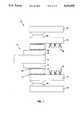
- FIG. 1shows an electrical backplane 10 according to the invention.
- the electrical backplane 10electrically interconnects logic boards, for example, 12, in a computer system.
- a logic board 12is comprised of a Substrate Power Bus (SPB) 14, with Low Density Interconnect (LDI) substrates 16 mounted on either side thereof.
- High Density Interconnect (HDI) substrates(not shown) may be mounted on top of the LDI substrates 16. Further information on the logic boards 12 is disclosed in the co-pending and commonly assigned application Ser. No. 07/444,747 filed on Dec. 1, 1989 by L. T. Shepherd et al.
- An assembly pressure connector 18is mounted adjacent each of the LDI substrates 16, so that one surface of the assembly pressure connector 18 lies in a closely-spaced parallel relationship with the surface of the LDI substrate 16. Electrical contact bumps 20 on the surface of the assembly pressure connector 18 are aligned with contact points (not shown) on the surface of the LDI substrate 16.
- the assembly pressure connector 18is also mounted adjacent to a connector interconnect board 22.
- the surface of the assembly pressure connector 18 opposite the LDI substrate 16lies in a closely-spaced parallel relationship with the surface of the connector interconnect board 22.
- Electrical contact bumps 24 on the surface of the assembly pressure connector 18are aligned with contact points (not shown) on the surface of the connector interconnect board 26.
- a bladder 26forces the surface of the connector interconnect board 22 against the surface of the assembly pressure connector 18, which in turn, forces the surface of the assembly pressure connector 18 against the surface of the LDI substrate 16.
- a push-pull or turn-key cammay be substituted for the bladder 26.
- the bumps 20 on the assembly pressure connector 18are thereby brought into electrical contact with the contact points on the LDI substrate 16.
- the bumps 24 on the assembly pressure connector 18are also thereby brought into electrical contact with the contact points on the connector interconnect board 22.
- the assembly pressure connector 18thus electrically interconnects the LDI substrate 16 with the connector interconnect board 22.
- the connector interconnect board 22is preferably a multi-layer PCB.
- the contact points thereonare electrically connected to traces (not shown) on or in the connector interconnect board 22.
- the tracesare electrically connected to external wiring.
- the tracesare connected to twisted pair wiring 28.
- the connector interconnect board 22provides for the connection of 1374 twisted pairs 28.
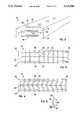
- FIG. 2shows an end view of the assembly pressure connector 18.
- the layers 32, 34, and 36 comprising the housing 30are manufactured of cellulose acetate butyrate.
- the top layer 32 and bottom layer 36are preferably rectangular with dimensions measuring 5.50 inches long by 0.280 inches wide by 0.020 thick.
- the middle layer 34is preferably rectangular with dimensions measuring 5.500 inches long by 0.280 inches wide by 0.030 inches thick.
- a plurality of axially-aligned hole combinations 38, 40, and 42extend through all three layers 32, 34, and 36 of the housing 30.
- the holes 38, 40, and 42are preferably made by accurately drilling through the housing 30.
- Holes 38 and 42are preferably 5.9 mils in diameter.
- Holes 40are preferably 10.6 mils in diameter.
- FIG. 3shows a cross-sectional view of the assembly pressure connector 18 that better describes its configuration.
- the hole combinations 38, 40, and 42are aligned and a 1 inch length of 4 mil diameter gold-plated beryllium-copper wire 44 is inserted therethrough.
- top layer 32 and bottom layer 36are held rigid, and the middle layer 34 is pushed, pulled, or otherwise shifted in relation to layers 32 and 36, to bend the wires 44.
- the screw arrangement 46shifts the middle layer 34. The leaf-spring effect keeps the ires 44 from permanently deforming.
- end portions 52 and 54 of the wires 44extend through the top layer 32 and bottom layer 36 of the assembly pressure connector 18. After bending, the end portions 52 and 54 of the wire 44 are trimmed as close as possible to the surface of the assembly pressure connector 18. The ends 52 and 54 are then milled using, for example, a mini-tool or a Dremel bit. The end portions 52 and 54 are then plated with gold to enhance their electrical interconnection with the contact points on the LDI substrate 16 and connector interconnect board 22.
- a first alternative embodimentcould file the end portions 52 and 54 of the wire, although this technique has a greater tendency to bend the wire 44 and stress the holes 38, 40, and 42.
- a second alternative embodimentcould use a bead blaster to achieve rounded end portions 52 and 54 for the wire 44.
- a third alternative embodimentcould use precut precision wire 44.
- pressureis not only created in the vertical direction 48 by the compressed wires 44, but a horizontal scrubbing action 50 is created that ensures improved electrical contact between the bumps, i.e., the end portions 52 and 54 of the wires 44, and the contact points on either the connector interconnect board of the LDI substrate.
- neither end 52 nor end 54is secured to the surface of the LDI substrate 16 or connector interconnect board 22.
- one or both ends 52 or 54 of the wire 44may be secured to the contact point, typically by soldering.
- the inventionprovides an electrical backplane for high density electrical connections with logic boards in a computer system.
- the electrical backplaneis comprised of an assembly pressure connector and a connector interconnect board that connects the logic boards to external wiring.
- the assembly pressure connectorhas electrical contact bumps on its surfaces for making electrical connections with contact points on the surface of the logic boards.
- the assembly pressure connectorprevents the permanent deformation of its electrical contact bumps by using resilient bumps.
- the resilient bumpsare formed from the end portions of interconnecting wires extending through the assembly pressure connector.
- the interconnecting wiresare bent in the shape of a leaf spring. Thus, the wires are compressed within the elastic range of their composing material and are not permanently deformed by the force applied to the assembly pressure connector.
Landscapes
- Engineering & Computer Science (AREA)
- General Engineering & Computer Science (AREA)
- Theoretical Computer Science (AREA)
- Computer Hardware Design (AREA)
- Physics & Mathematics (AREA)
- General Physics & Mathematics (AREA)
- Coupling Device And Connection With Printed Circuit (AREA)
Abstract
Description
Claims (3)
Priority Applications (1)
| Application Number | Priority Date | Filing Date | Title |
|---|---|---|---|
| US07/556,024US5123848A (en) | 1990-07-20 | 1990-07-20 | Computer signal interconnect apparatus |
Applications Claiming Priority (1)
| Application Number | Priority Date | Filing Date | Title |
|---|---|---|---|
| US07/556,024US5123848A (en) | 1990-07-20 | 1990-07-20 | Computer signal interconnect apparatus |
Publications (1)
| Publication Number | Publication Date |
|---|---|
| US5123848Atrue US5123848A (en) | 1992-06-23 |
Family
ID=24219570
Family Applications (1)
| Application Number | Title | Priority Date | Filing Date |
|---|---|---|---|
| US07/556,024Expired - LifetimeUS5123848A (en) | 1990-07-20 | 1990-07-20 | Computer signal interconnect apparatus |
Country Status (1)
| Country | Link |
|---|---|
| US (1) | US5123848A (en) |
Cited By (10)
| Publication number | Priority date | Publication date | Assignee | Title |
|---|---|---|---|---|
| US5385477A (en)* | 1993-07-30 | 1995-01-31 | Ck Technologies, Inc. | Contactor with elastomer encapsulated probes |
| US5611696A (en)* | 1994-12-14 | 1997-03-18 | International Business Machines Corporation | High density and high current capacity pad-to-pad connector comprising of spring connector elements (SCE) |
| EP0915342A3 (en)* | 1997-11-05 | 2001-01-24 | Feinmetall GmbH | Test head for microstructures with interface |
| US6205532B1 (en) | 1998-05-22 | 2001-03-20 | Avici Systems, Inc. | Apparatus and methods for connecting modules using remote switching |
| US6285679B1 (en) | 1997-08-22 | 2001-09-04 | Avici Systems, Inc. | Methods and apparatus for event-driven routing |
| US6370145B1 (en) | 1997-08-22 | 2002-04-09 | Avici Systems | Internet switch router |
| US6709279B2 (en)* | 2000-12-28 | 2004-03-23 | Yamaichi Electronics Co., Ltd. | Contact pin module and testing device provided with the same |
| US6832917B1 (en) | 2004-01-16 | 2004-12-21 | Intercon Systems, Inc. | Interposer assembly |
| US20120152602A1 (en)* | 2010-12-15 | 2012-06-21 | Hon Hai Precision Industry Co., Ltd. | Printed circuit board |
| US20140115876A1 (en)* | 2012-10-31 | 2014-05-01 | Toyota Jidosha Kabushiki Kaisha | Manufacturing method of segment coil |
Citations (41)
| Publication number | Priority date | Publication date | Assignee | Title |
|---|---|---|---|---|
| CA608258A (en)* | 1960-11-08 | Johnson, Matthey And Mallory Limited | Spring pin cascaded circuits | |
| US3212049A (en)* | 1963-04-30 | 1965-10-12 | Ind Electronic Hardware Corp | Multilayer circuitry with placed bushings |
| US3370203A (en)* | 1965-07-19 | 1968-02-20 | United Aircraft Corp | Integrated circuit modules |
| US3400358A (en)* | 1965-10-21 | 1968-09-03 | Ibm | Electrical connector |
| US3526869A (en)* | 1969-01-21 | 1970-09-01 | Itt | Cam actuated printed circuit board connector |
| US3529213A (en)* | 1969-04-08 | 1970-09-15 | North American Rockwell | Extendable package for electronic assemblies |
| US3537063A (en)* | 1968-06-17 | 1970-10-27 | Ibm | Circuit card connector |
| US3541490A (en)* | 1967-08-21 | 1970-11-17 | Quentin Berg | Connector block |
| US3576515A (en)* | 1968-08-27 | 1971-04-27 | Amp Inc | Printed circuit edge connector |
| US3793609A (en)* | 1971-12-13 | 1974-02-19 | Microdot Inc | Low insertion force printed board connector |
| US3899234A (en)* | 1974-03-20 | 1975-08-12 | Amp Inc | Low insertion force cam actuated printed circuit board connector |
| US3977747A (en)* | 1974-10-10 | 1976-08-31 | Bunker Ramo Corporation | Zero insertion force connector |
| US3982807A (en)* | 1975-03-27 | 1976-09-28 | International Telephone And Telegraph Corporation | Zero force printed circuit board connector |
| US4080027A (en)* | 1976-07-30 | 1978-03-21 | Gte Sylvania Incorporated | Electrical contact and connector |
| US4159154A (en)* | 1978-04-10 | 1979-06-26 | International Telephone And Telegraph Corporation | Zero insertion force connector |
| US4159861A (en)* | 1977-12-30 | 1979-07-03 | International Telephone And Telegraph Corporation | Zero insertion force connector |
| US4178053A (en)* | 1978-02-13 | 1979-12-11 | Ncr Corporation | Zero-insertion force electrical connector |
| US4220382A (en)* | 1978-12-15 | 1980-09-02 | Amp Incorporated | Bussing connector |
| US4327955A (en)* | 1979-09-24 | 1982-05-04 | Minter Jerry B | Reduced insertion force connector |
| US4350402A (en)* | 1980-09-17 | 1982-09-21 | Amp Incorporated | Board mount zero insertion force connector |
| US4352533A (en)* | 1978-10-31 | 1982-10-05 | Fujitsu Limited | Connector device for printed boards |
| DE3123627A1 (en)* | 1981-06-15 | 1982-12-30 | Siemens AG, 1000 Berlin und 8000 München | DEVICE FOR SIMULTANEOUSLY CONTACTING MULTIPLE CLOSE-UP CHECK POINTS, IN PARTICULAR OF GRID FIELDS |
| US4392700A (en)* | 1981-09-08 | 1983-07-12 | Amp Incorporated | Cam actuated zero insertion force mother/daughter board connector |
| US4400049A (en)* | 1981-08-12 | 1983-08-23 | Ncr Corporation | Connector for interconnecting circuit boards |
| US4423376A (en)* | 1981-03-20 | 1983-12-27 | International Business Machines Corporation | Contact probe assembly having rotatable contacting probe elements |
| US4428635A (en)* | 1982-02-24 | 1984-01-31 | Amp Incorporated | One piece zif connector |
| US4445735A (en)* | 1980-12-05 | 1984-05-01 | Compagnie Internationale Pour L'informatique Cii-Honeywell Bull (Societe Anonyme) | Electrical connection device for high density contacts |
| US4540228A (en)* | 1983-06-27 | 1985-09-10 | Sperry Corporation | Low insertion force connector with improved cam actuator |
| US4560221A (en)* | 1984-05-14 | 1985-12-24 | Amp Incorporated | High density zero insertion force connector |
| US4591218A (en)* | 1983-08-29 | 1986-05-27 | Gte Communication Systems Corporation | Low insertion force connection arrangement |
| US4591219A (en)* | 1983-08-29 | 1986-05-27 | Gte Communication Systems Corporation | Low insertion force connection arrangement |
| US4597619A (en)* | 1983-08-29 | 1986-07-01 | Gte Communication Systems Corporation | Low insertion force connection arrangement |
| US4626056A (en)* | 1984-02-21 | 1986-12-02 | Amp Incorporated | Card edge connector |
| US4629270A (en)* | 1984-07-16 | 1986-12-16 | Amp Incorporated | Zero insertion force card edge connector with flexible film circuitry |
| US4684194A (en)* | 1984-07-16 | 1987-08-04 | Trw Inc. | Zero insertion force connector |
| US4700996A (en)* | 1986-10-08 | 1987-10-20 | Cray Research, Inc. | ZIE edge connector |
| USRE32559E (en)* | 1982-12-27 | 1987-12-15 | Amp Incorporated | Card edge connector locking device |
| US4744764A (en)* | 1986-05-27 | 1988-05-17 | Rogers Corporation | Connector arrangement |
| US4806104A (en)* | 1988-02-09 | 1989-02-21 | Itt Corporation | High density connector |
| US4911645A (en)* | 1988-12-14 | 1990-03-27 | Cray Research, Inc. | Parallel board ZIF module connector |
| US4998886A (en)* | 1989-07-07 | 1991-03-12 | Teledyne Kinetics | High density stacking connector |
- 1990
- 1990-07-20USUS07/556,024patent/US5123848A/ennot_activeExpired - Lifetime
Patent Citations (42)
| Publication number | Priority date | Publication date | Assignee | Title |
|---|---|---|---|---|
| CA608258A (en)* | 1960-11-08 | Johnson, Matthey And Mallory Limited | Spring pin cascaded circuits | |
| US3212049A (en)* | 1963-04-30 | 1965-10-12 | Ind Electronic Hardware Corp | Multilayer circuitry with placed bushings |
| US3370203A (en)* | 1965-07-19 | 1968-02-20 | United Aircraft Corp | Integrated circuit modules |
| US3400358A (en)* | 1965-10-21 | 1968-09-03 | Ibm | Electrical connector |
| US3541490A (en)* | 1967-08-21 | 1970-11-17 | Quentin Berg | Connector block |
| US3537063A (en)* | 1968-06-17 | 1970-10-27 | Ibm | Circuit card connector |
| US3576515A (en)* | 1968-08-27 | 1971-04-27 | Amp Inc | Printed circuit edge connector |
| US3526869A (en)* | 1969-01-21 | 1970-09-01 | Itt | Cam actuated printed circuit board connector |
| US3529213A (en)* | 1969-04-08 | 1970-09-15 | North American Rockwell | Extendable package for electronic assemblies |
| US3793609A (en)* | 1971-12-13 | 1974-02-19 | Microdot Inc | Low insertion force printed board connector |
| US3899234A (en)* | 1974-03-20 | 1975-08-12 | Amp Inc | Low insertion force cam actuated printed circuit board connector |
| US3977747A (en)* | 1974-10-10 | 1976-08-31 | Bunker Ramo Corporation | Zero insertion force connector |
| US3982807A (en)* | 1975-03-27 | 1976-09-28 | International Telephone And Telegraph Corporation | Zero force printed circuit board connector |
| US4080027A (en)* | 1976-07-30 | 1978-03-21 | Gte Sylvania Incorporated | Electrical contact and connector |
| US4159861A (en)* | 1977-12-30 | 1979-07-03 | International Telephone And Telegraph Corporation | Zero insertion force connector |
| US4178053A (en)* | 1978-02-13 | 1979-12-11 | Ncr Corporation | Zero-insertion force electrical connector |
| US4159154A (en)* | 1978-04-10 | 1979-06-26 | International Telephone And Telegraph Corporation | Zero insertion force connector |
| US4352533A (en)* | 1978-10-31 | 1982-10-05 | Fujitsu Limited | Connector device for printed boards |
| US4220382A (en)* | 1978-12-15 | 1980-09-02 | Amp Incorporated | Bussing connector |
| US4327955A (en)* | 1979-09-24 | 1982-05-04 | Minter Jerry B | Reduced insertion force connector |
| US4350402A (en)* | 1980-09-17 | 1982-09-21 | Amp Incorporated | Board mount zero insertion force connector |
| US4445735A (en)* | 1980-12-05 | 1984-05-01 | Compagnie Internationale Pour L'informatique Cii-Honeywell Bull (Societe Anonyme) | Electrical connection device for high density contacts |
| US4423376A (en)* | 1981-03-20 | 1983-12-27 | International Business Machines Corporation | Contact probe assembly having rotatable contacting probe elements |
| DE3123627A1 (en)* | 1981-06-15 | 1982-12-30 | Siemens AG, 1000 Berlin und 8000 München | DEVICE FOR SIMULTANEOUSLY CONTACTING MULTIPLE CLOSE-UP CHECK POINTS, IN PARTICULAR OF GRID FIELDS |
| US4400049A (en)* | 1981-08-12 | 1983-08-23 | Ncr Corporation | Connector for interconnecting circuit boards |
| US4392700A (en)* | 1981-09-08 | 1983-07-12 | Amp Incorporated | Cam actuated zero insertion force mother/daughter board connector |
| US4428635A (en)* | 1982-02-24 | 1984-01-31 | Amp Incorporated | One piece zif connector |
| USRE32559E (en)* | 1982-12-27 | 1987-12-15 | Amp Incorporated | Card edge connector locking device |
| US4540228A (en)* | 1983-06-27 | 1985-09-10 | Sperry Corporation | Low insertion force connector with improved cam actuator |
| US4591218A (en)* | 1983-08-29 | 1986-05-27 | Gte Communication Systems Corporation | Low insertion force connection arrangement |
| US4591219A (en)* | 1983-08-29 | 1986-05-27 | Gte Communication Systems Corporation | Low insertion force connection arrangement |
| US4597619A (en)* | 1983-08-29 | 1986-07-01 | Gte Communication Systems Corporation | Low insertion force connection arrangement |
| US4626056A (en)* | 1984-02-21 | 1986-12-02 | Amp Incorporated | Card edge connector |
| US4560221A (en)* | 1984-05-14 | 1985-12-24 | Amp Incorporated | High density zero insertion force connector |
| US4684194A (en)* | 1984-07-16 | 1987-08-04 | Trw Inc. | Zero insertion force connector |
| US4629270A (en)* | 1984-07-16 | 1986-12-16 | Amp Incorporated | Zero insertion force card edge connector with flexible film circuitry |
| US4744764A (en)* | 1986-05-27 | 1988-05-17 | Rogers Corporation | Connector arrangement |
| US4700996A (en)* | 1986-10-08 | 1987-10-20 | Cray Research, Inc. | ZIE edge connector |
| EP0263585A2 (en)* | 1986-10-08 | 1988-04-13 | Cray Research, Inc. | Zif edge connector |
| US4806104A (en)* | 1988-02-09 | 1989-02-21 | Itt Corporation | High density connector |
| US4911645A (en)* | 1988-12-14 | 1990-03-27 | Cray Research, Inc. | Parallel board ZIF module connector |
| US4998886A (en)* | 1989-07-07 | 1991-03-12 | Teledyne Kinetics | High density stacking connector |
Non-Patent Citations (4)
| Title |
|---|
| IBM Bulletin, Faure, vol. 17, No. 2, p. 444, Jul. 1974.* |
| IBM Bulletin, Schick, vol. 6, No. 10, p. 66, Mar. 1964.* |
| ITT Cannon Connectors Catalog, 1984 1985, p. 280.* |
| ITT Cannon Connectors Catalog, 1984-1985, p. 280. |
Cited By (21)
| Publication number | Priority date | Publication date | Assignee | Title |
|---|---|---|---|---|
| US5385477A (en)* | 1993-07-30 | 1995-01-31 | Ck Technologies, Inc. | Contactor with elastomer encapsulated probes |
| WO1995004447A1 (en)* | 1993-07-30 | 1995-02-09 | Ck Technologies, Inc. | Buckling beam test probe with elastomer encapsulated probe wires |
| US5611696A (en)* | 1994-12-14 | 1997-03-18 | International Business Machines Corporation | High density and high current capacity pad-to-pad connector comprising of spring connector elements (SCE) |
| US20030118048A1 (en)* | 1997-08-22 | 2003-06-26 | Avici Systems | Internet switch router |
| US8325715B2 (en) | 1997-08-22 | 2012-12-04 | Futurewei Technologies, Inc. | Internet switch router |
| US6285679B1 (en) | 1997-08-22 | 2001-09-04 | Avici Systems, Inc. | Methods and apparatus for event-driven routing |
| US6370145B1 (en) | 1997-08-22 | 2002-04-09 | Avici Systems | Internet switch router |
| US6563831B1 (en) | 1997-08-22 | 2003-05-13 | Avici Systems | Router with virtual channel allocation |
| US7187679B2 (en) | 1997-08-22 | 2007-03-06 | Avici Systems, Inc. | Internet switch router |
| US6654381B2 (en) | 1997-08-22 | 2003-11-25 | Avici Systems, Inc. | Methods and apparatus for event-driven routing |
| US20070140240A1 (en)* | 1997-08-22 | 2007-06-21 | Dally William J | Internet switch router |
| US20040160970A1 (en)* | 1997-08-22 | 2004-08-19 | Avici Systems, Inc. | Methods and apparatus for event-driven routing |
| US6417684B1 (en) | 1997-11-05 | 2002-07-09 | Feinmetall Gmbh | Securement of test points in a test head |
| EP0915342A3 (en)* | 1997-11-05 | 2001-01-24 | Feinmetall GmbH | Test head for microstructures with interface |
| US6606656B2 (en) | 1998-05-22 | 2003-08-12 | Avici Systems, Inc. | Apparatus and methods for connecting modules using remote switching |
| US6976064B2 (en) | 1998-05-22 | 2005-12-13 | Avici Systems, Inc. | Apparatus and methods for connecting modules using remote switching |
| US6205532B1 (en) | 1998-05-22 | 2001-03-20 | Avici Systems, Inc. | Apparatus and methods for connecting modules using remote switching |
| US6709279B2 (en)* | 2000-12-28 | 2004-03-23 | Yamaichi Electronics Co., Ltd. | Contact pin module and testing device provided with the same |
| US6832917B1 (en) | 2004-01-16 | 2004-12-21 | Intercon Systems, Inc. | Interposer assembly |
| US20120152602A1 (en)* | 2010-12-15 | 2012-06-21 | Hon Hai Precision Industry Co., Ltd. | Printed circuit board |
| US20140115876A1 (en)* | 2012-10-31 | 2014-05-01 | Toyota Jidosha Kabushiki Kaisha | Manufacturing method of segment coil |
Similar Documents
| Publication | Publication Date | Title |
|---|---|---|
| EP0699354B1 (en) | Planar cable array | |
| US6358064B2 (en) | Z-axis electrical interconnect | |
| US5118300A (en) | Active electrical connector | |
| US7417871B2 (en) | Memory module | |
| US4992052A (en) | Modular connector system with high contact element density | |
| US7227759B2 (en) | Signal-segregating connector system | |
| US5386344A (en) | Flex circuit card elastomeric cable connector assembly | |
| US5137456A (en) | High density, separable connector and contact for use therein | |
| US6273759B1 (en) | Multi-slot connector with integrated bus providing contact between adjacent modules | |
| EP0147039A2 (en) | Surface mount connector | |
| WO2002003462A2 (en) | Self retained pressure connection | |
| JP3343719B2 (en) | Right angle connector for cable | |
| JPH0757831A (en) | Connector for substrate connection | |
| US5123848A (en) | Computer signal interconnect apparatus | |
| JPH0888062A (en) | Connector and board mounting method | |
| JPH06223895A (en) | Connector and its method | |
| US4645277A (en) | Connector for connecting boards | |
| US6074220A (en) | Direct circuit to circuit stored energy connector | |
| US5554036A (en) | Circuit board electrical connector | |
| US5507654A (en) | Low profile electrical adaptor | |
| US5683256A (en) | Integral thru-hole contacts | |
| US6462955B1 (en) | Component alignment casing system | |
| EP0393251A1 (en) | Modular connector system with high contact element density surface mounted connectors | |
| JPS63146370A (en) | Connector and manufacture thereof | |
| GB2092839A (en) | Improvements in or relating to electrical connection arrangements |
Legal Events
| Date | Code | Title | Description |
|---|---|---|---|
| AS | Assignment | Owner name:CRAY RESEARCH, INC., A CORP OF DE, MINNESOTA Free format text:ASSIGNMENT OF ASSIGNORS INTEREST.;ASSIGNORS:AUGUST, MELVIN C.;NEBEL, MARY;NEUMANN, EUGENE F.;REEL/FRAME:005378/0797 Effective date:19900627 | |
| STCF | Information on status: patent grant | Free format text:PATENTED CASE | |
| CC | Certificate of correction | ||
| FEPP | Fee payment procedure | Free format text:PAYOR NUMBER ASSIGNED (ORIGINAL EVENT CODE: ASPN); ENTITY STATUS OF PATENT OWNER: LARGE ENTITY | |
| FPAY | Fee payment | Year of fee payment:4 | |
| FPAY | Fee payment | Year of fee payment:8 | |
| AS | Assignment | Owner name:TERA COMPUTER COMPANY, WASHINGTON Free format text:ASSIGNMENT OF ASSIGNORS INTEREST;ASSIGNOR:CRAY RESEARCH, L.L.C.;REEL/FRAME:011231/0132 Effective date:20000524 | |
| AS | Assignment | Owner name:CRAY, INC., WASHINGTON Free format text:CHANGE OF NAME;ASSIGNOR:TERA COMPUTER COMPANY;REEL/FRAME:011712/0145 Effective date:20010423 | |
| AS | Assignment | Owner name:FOOTHILL CAPITAL CORPORATION (A CALIFORNIA CORPORA Free format text:SECURITY INTEREST;ASSIGNOR:CRAY, INC. (A WASHINGTON CORPORATION);REEL/FRAME:011763/0716 Effective date:20010328 | |
| AS | Assignment | Owner name:CRAY INC., WASHINGTON Free format text:CORRECTIVE ASSIGNMENT TO CORRECT THE NAME OF THE ASSIGNEE, FILED ON 12-31-2001. RECORDED ON REEL 012322, FRAME 0143;ASSIGNOR:TERA COMPUTER COMPANY;REEL/FRAME:012322/0143 Effective date:20000403 | |
| FPAY | Fee payment | Year of fee payment:12 | |
| AS | Assignment | Owner name:WELLS FARGO BANK, N.A.,CALIFORNIA Free format text:SECURITY AGREEMENT;ASSIGNOR:CRAY INC.;REEL/FRAME:016446/0675 Effective date:20050531 Owner name:WELLS FARGO BANK, N.A., CALIFORNIA Free format text:SECURITY AGREEMENT;ASSIGNOR:CRAY INC.;REEL/FRAME:016446/0675 Effective date:20050531 |