US5122988A - Data stream smoothing using a FIFO memory - Google Patents
Data stream smoothing using a FIFO memoryDownload PDFInfo
- Publication number
- US5122988A US5122988AUS07/732,351US73235191AUS5122988AUS 5122988 AUS5122988 AUS 5122988AUS 73235191 AUS73235191 AUS 73235191AUS 5122988 AUS5122988 AUS 5122988A
- Authority
- US
- United States
- Prior art keywords
- memory
- dram
- refresh
- signal
- fifo memory
- Prior art date
- Legal status (The legal status is an assumption and is not a legal conclusion. Google has not performed a legal analysis and makes no representation as to the accuracy of the status listed.)
- Expired - Lifetime
Links
Images

Classifications
- G—PHYSICS
- G06—COMPUTING OR CALCULATING; COUNTING
- G06F—ELECTRIC DIGITAL DATA PROCESSING
- G06F5/00—Methods or arrangements for data conversion without changing the order or content of the data handled
- G06F5/06—Methods or arrangements for data conversion without changing the order or content of the data handled for changing the speed of data flow, i.e. speed regularising or timing, e.g. delay lines, FIFO buffers; over- or underrun control therefor
- G06F5/10—Methods or arrangements for data conversion without changing the order or content of the data handled for changing the speed of data flow, i.e. speed regularising or timing, e.g. delay lines, FIFO buffers; over- or underrun control therefor having a sequence of storage locations each being individually accessible for both enqueue and dequeue operations, e.g. using random access memory
- G06F5/12—Means for monitoring the fill level; Means for resolving contention, i.e. conflicts between simultaneous enqueue and dequeue operations
- G06F5/14—Means for monitoring the fill level; Means for resolving contention, i.e. conflicts between simultaneous enqueue and dequeue operations for overflow or underflow handling, e.g. full or empty flags
- G—PHYSICS
- G01—MEASURING; TESTING
- G01R—MEASURING ELECTRIC VARIABLES; MEASURING MAGNETIC VARIABLES
- G01R31/00—Arrangements for testing electric properties; Arrangements for locating electric faults; Arrangements for electrical testing characterised by what is being tested not provided for elsewhere
- G01R31/28—Testing of electronic circuits, e.g. by signal tracer
- G01R31/317—Testing of digital circuits
- G01R31/3181—Functional testing
- G01R31/319—Tester hardware, i.e. output processing circuits
- G01R31/31917—Stimuli generation or application of test patterns to the device under test [DUT]
- G01R31/31919—Storing and outputting test patterns
- G—PHYSICS
- G11—INFORMATION STORAGE
- G11C—STATIC STORES
- G11C11/00—Digital stores characterised by the use of particular electric or magnetic storage elements; Storage elements therefor
- G11C11/21—Digital stores characterised by the use of particular electric or magnetic storage elements; Storage elements therefor using electric elements
- G11C11/34—Digital stores characterised by the use of particular electric or magnetic storage elements; Storage elements therefor using electric elements using semiconductor devices
- G11C11/40—Digital stores characterised by the use of particular electric or magnetic storage elements; Storage elements therefor using electric elements using semiconductor devices using transistors
- G11C11/401—Digital stores characterised by the use of particular electric or magnetic storage elements; Storage elements therefor using electric elements using semiconductor devices using transistors forming cells needing refreshing or charge regeneration, i.e. dynamic cells
- G11C11/406—Management or control of the refreshing or charge-regeneration cycles
Definitions
- This inventionrelates to integrated circuit testing devices, and more particularly to the use of a FIFO memory to promote uniform communication of test data from a dynamic random access memory (DRAM) to a device under test.
- DRAMdynamic random access memory
- LSI component testersAs large scale integrated circuit (LSI) components become more complex, the need for larger local memory in LSI component testers increases accordingly. For example, state of the art LSI component testers must have the capability of storing up to eight million or more vectors in local memory. The increase is caused by the ever increasing length of test patterns for complex devices, especially those which are CAD generated. Because of such memory requirements, it is desirable to use dynamic random access memories (DRAM's) as the components used in building the local memories because they provide the largest amount of storage per dollar.
- DRAM'sdynamic random access memories
- a DRAM running in one of the fast access modescan do only a limited number of fast accesses before it must revert to a normal, slower write or read cycle.
- a DRAM running in one of the fast access modese.g., static column mode, page mode. nibble mode, etc.
- static column mode cyclescan be 60 ns, the longer cycle which occurs when crossing a row boundary is at least twice as long. This amounts to a break in the smooth data stream.
- the present inventionis directed to the use of a FIFO memory for communicating data from a DRAM to a testing device in a continuous data stream despite interruptions for refresh cycles or long memory access cycles. Unnecessary duplication of circuitry is eliminated, together with the added control circuitry required of such duplicate systems.
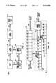
- FIG. 1is a block diagram of a particular embodiment of an LSI testing device according to the present invention.
- FIG. 2is a block diagram of a particular embodiment of the FIFO memory and memory status circuit shown in FIG. 1.
- FIG. 4is a block diagram of a particular embodiment of the memory access counter shown in FIG. 3.
- FIG. 1is a block diagram of a memory test system 10 according to the present invention.
- Test system 10includes a DRAM 14 for storing data used in the testing process, a FIFO memory 18 for receiving the data from DRAM 14 over a bus 22, a memory control circuit 26 which communicates with FIFO memory 18 over a bus 30 for monitoring the status of FIFO memory 18, and a DRAM address/refresh circuit 34 for receiving FIFO memory status information from memory control circuit 26 over a bus 38 and for controlling the addressing and refresh of DRAM 14 through a bus 42.
- the data in FIFO memory 18is communicated to a test station 46 over a bus 50 at a substantially uninterrupted rate.
- Test station 46formats the data from FIFO memory 18 and communicates the formatted data to a device under test 54 over a bus 58 for testing the device.
- FIG. 2is a more detailed block diagram of FIFO memory 18 and memory control circuit 26.
- FIFO memory 18comprises a plurality of latches 62 for moving data from DRAM 14 to test station 46.
- Memory control circuit 26comprises a read address register 66, a write address register 70 and a memory status circuit 74.
- Read address register 66comprises a plurality of flip-flops 78 which are interconnected to form a shifter wherein the output of the last flip-flop is coupled to the input of the first flip-flop so that a binary sequence may be shifted in a continuous ring.
- only one active bit (a one)exists in the address register at any one time, and the remaining bits are all zero.
- flip-flop 78there is one flip-flop 78 per latch 62 in FIFO memory 18, and the flip-flop which contains the active bit determines which latch 62 has been read most recently.
- the bit configuration in read address register 66is communicated to memory status circuit 74 over a bus 82.
- Write address register 70comprises a plurality of flip-flops 84 which are connected together and function in the same way as read address register 66. In this case, the single active bit within write address register 70 corresponds to the most recently written to latch 62 in FIFO memory 18. The bit configuration of write address register 70 is communicated to memory status circuit 74 over a bus 88. Buses 82 and 88 form a part of bus 30 in FIG. 1.
- Memory status circuit 74receives the bit patterns from read address register 66 and write address register 70 and determines, from the relative location of the most recently read from and written to latches, the state of FIFO memory 18. In particular, memory status circuit 74 determines whether or not FIFO memory is "full" through the use of suitable combinational logic. In this embodiment, FIFO memory 18 is full whenever 8, 9 or 10 latches 62 in FIFO memory 18 contain data that has yet to be sent to test station 46. When memory status circuit 74 determines that FIFO memory 18 is full, it provides a memory-full status signal on bus 38 to DRAM access/refresh circuit 34.
- FIG. 3is a more detailed block diagram of DRAM access/refresh circuit 34.
- DRAM access/refresh circuit 34comprises a memory access control circuit 92, a refresh timer 96, a refresh counter 100 and a memory access counter 112.
- Refresh timer 96provides a "refresh due" signal on a bus 104 whenever DRAM 14 should be refreshed.
- the time interval after which the refresh due signal is generatedtypically is determined by the size of the DRAM and the amount of time by which the entire DRAM must be refreshed. For example, if the entire memory must be refreshed every eight milliseconds, and if the DRAM contains 512 rows of data, then a refresh due signal must be generated at least 512 times within the eight millisecond period.
- Refresh counter 100is a modulo-n counter where n equals the number of rows in DRAM 14.
- the value of refresh counter 100is communicated to memory access control circuit 92 over a bus 108 for sequentially refreshing each row in DRAM 14.
- Memory access counter 112provides DRAM address signals to memory access control circuit 92 over a bus 116.
- memory access counter 112comprises a column counter 120 and a row counter 124.
- Column counter 120provides the least significant bits (LSB's) of the DRAM address
- row counter 124provides the most significant bits (MSB's) of the DRAM address.
- Row counter 124operates in response to carry-out signals received from column counter 120 over a bus 128.
- the values of column counter 120 and row counter 124are output on bus 116.
- memory access control circuit 92In operation, memory access control circuit 92 generates DRAM read accesses in response to address signals received over bus 116 whenever FIFO memory 18 is less than full. Additionally, memory access control circuit 92 operates to refresh DRAM 14 in response to the memory status signal received from bus 38, the refresh due signal received from bus 104, and the row address received on bus 108. When a refresh due signal is received from refresh timer 96, memory access control 92 waits until the appropriate memory-full signal is received from memory control circuit 26. When this occurs, memory access control 92 refreshes the row in DRAM 14 addressed by row counter 100, typically by performing a memory access to that location.
- datamay be communicated from DRAM 14 to FIFO memory 18 at the DRAM data rate and thereafter read out of FIFO memory 18 at the rate required by test station 46, even if the two data rates are different.
- Datais communicated from DRAM 14 to FIFO memory 18 as long as FIFO memory is less than full. Refresh accesses are allowed when FIFO memory 18 is full.
- the FIFOcan also be used for DRAM loading with a higher data source rate uninterrupted by refresh requests.
- the FIFOis filled at a constant rate, and the FIFO logic generates DRAM write accesses whenever the FIFO is more than empty.
- This manner of loading local memoryallows the use of a synchronous source bus, and no handshakes are required. Consequently, the scope of the invention should not be limited except as described in the claims.
Landscapes
- Engineering & Computer Science (AREA)
- General Engineering & Computer Science (AREA)
- Physics & Mathematics (AREA)
- General Physics & Mathematics (AREA)
- Theoretical Computer Science (AREA)
- Microelectronics & Electronic Packaging (AREA)
- Computer Hardware Design (AREA)
- Dram (AREA)
Abstract
Description
Claims (16)
Applications Claiming Priority (1)
| Application Number | Priority Date | Filing Date | Title |
|---|---|---|---|
| US41076789A | 1989-09-21 | 1989-09-21 |
Related Parent Applications (1)
| Application Number | Title | Priority Date | Filing Date |
|---|---|---|---|
| US41076789AContinuation | 1989-09-21 | 1989-09-21 |
Publications (1)
| Publication Number | Publication Date |
|---|---|
| US5122988Atrue US5122988A (en) | 1992-06-16 |
Family
ID=23626131
Family Applications (1)
| Application Number | Title | Priority Date | Filing Date |
|---|---|---|---|
| US07/732,351Expired - LifetimeUS5122988A (en) | 1989-09-21 | 1991-07-17 | Data stream smoothing using a FIFO memory |
Country Status (1)
| Country | Link |
|---|---|
| US (1) | US5122988A (en) |
Cited By (20)
| Publication number | Priority date | Publication date | Assignee | Title |
|---|---|---|---|---|
| US5345574A (en)* | 1990-05-15 | 1994-09-06 | Seiko Epson Corporation | Memory card having controller providing adjustable refresh to a plurality of DRAMs |
| US5388074A (en)* | 1992-12-17 | 1995-02-07 | Vlsi Technology, Inc. | FIFO memory using single output register |
| US5412610A (en)* | 1993-06-29 | 1995-05-02 | Mitsubishi Denki Kabushiki Kaisha | Serial data transfer device |
| US5566188A (en)* | 1995-03-29 | 1996-10-15 | Teradyne, Inc. | Low cost timing generator for automatic test equipment operating at high data rates |
| US5617118A (en)* | 1991-06-10 | 1997-04-01 | International Business Machines Corporation | Mode dependent minimum FIFO fill level controls processor access to video memory |
| US6014764A (en)* | 1997-05-20 | 2000-01-11 | Schlumberger Technologies Inc. | Providing test vectors with pattern chaining definition |
| US6097655A (en)* | 1998-04-03 | 2000-08-01 | International Business Machines Corporation | Pull through FIFO memory device |
| US6286120B1 (en) | 1994-09-01 | 2001-09-04 | Teradyne, Inc. | Memory architecture for automatic test equipment using vector module table |
| US20040100943A1 (en)* | 2002-11-21 | 2004-05-27 | Kasper David J. | Managing a finite queue |
| US6748564B1 (en) | 2000-10-24 | 2004-06-08 | Nptest, Llc | Scan stream sequencing for testing integrated circuits |
| US20060087902A1 (en)* | 2003-09-30 | 2006-04-27 | Infineon Technologies Ag | Selective bank refresh |
| US20080098284A1 (en)* | 2006-10-18 | 2008-04-24 | Kencast, Inc. | Systems, methods, apparatus, and computer program products for providing forward error correction with low latency |
| US20080165605A1 (en)* | 2007-01-05 | 2008-07-10 | Innovative Silicon S.A. | Method and apparatus for variable memory cell refresh |
| US20080164149A1 (en)* | 2007-01-05 | 2008-07-10 | Artz Matthew R | Rapid gel electrophoresis system |
| US20100218074A1 (en)* | 2005-02-17 | 2010-08-26 | Kencast, Inc. | System, Method and Apparatus for Reducing Blockage Losses on Information Distribution Networks |
| US20170085331A1 (en)* | 2015-09-18 | 2017-03-23 | Qualcomm Incorporated | Synchronization of endpoints using tunable latency |
| US20170132144A1 (en)* | 2014-03-29 | 2017-05-11 | Empire Technology Development Llc | Energy-efficient dynamic dram cache sizing |
| US9990293B2 (en) | 2014-08-12 | 2018-06-05 | Empire Technology Development Llc | Energy-efficient dynamic dram cache sizing via selective refresh of a cache in a dram |
| US20200168270A1 (en)* | 2018-11-26 | 2020-05-28 | Birad - Research & Development Company Ltd. | Refresh controller for first-in first-out memories |
| CN112114747A (en)* | 2020-08-31 | 2020-12-22 | 山东华芯半导体有限公司 | Method for improving NAND Flash read stability in SSD |
Citations (5)
| Publication number | Priority date | Publication date | Assignee | Title |
|---|---|---|---|---|
| US4631701A (en)* | 1983-10-31 | 1986-12-23 | Ncr Corporation | Dynamic random access memory refresh control system |
| US4642797A (en)* | 1983-11-10 | 1987-02-10 | Monolithic Memories, Inc. | High speed first-in-first-out memory |
| US4777624A (en)* | 1985-07-16 | 1988-10-11 | Fuji-Xerox Company, Ltd. | Dynamic memory device |
| US4882710A (en)* | 1986-09-18 | 1989-11-21 | Texas Instruments Incorporated | FIFO memory including dynamic memory elements |
| US4891788A (en)* | 1988-05-09 | 1990-01-02 | Kreifels Gerard A | FIFO with almost full/almost empty flag |
- 1991
- 1991-07-17USUS07/732,351patent/US5122988A/ennot_activeExpired - Lifetime
Patent Citations (5)
| Publication number | Priority date | Publication date | Assignee | Title |
|---|---|---|---|---|
| US4631701A (en)* | 1983-10-31 | 1986-12-23 | Ncr Corporation | Dynamic random access memory refresh control system |
| US4642797A (en)* | 1983-11-10 | 1987-02-10 | Monolithic Memories, Inc. | High speed first-in-first-out memory |
| US4777624A (en)* | 1985-07-16 | 1988-10-11 | Fuji-Xerox Company, Ltd. | Dynamic memory device |
| US4882710A (en)* | 1986-09-18 | 1989-11-21 | Texas Instruments Incorporated | FIFO memory including dynamic memory elements |
| US4891788A (en)* | 1988-05-09 | 1990-01-02 | Kreifels Gerard A | FIFO with almost full/almost empty flag |
Cited By (34)
| Publication number | Priority date | Publication date | Assignee | Title |
|---|---|---|---|---|
| US5345574A (en)* | 1990-05-15 | 1994-09-06 | Seiko Epson Corporation | Memory card having controller providing adjustable refresh to a plurality of DRAMs |
| US5617118A (en)* | 1991-06-10 | 1997-04-01 | International Business Machines Corporation | Mode dependent minimum FIFO fill level controls processor access to video memory |
| US5388074A (en)* | 1992-12-17 | 1995-02-07 | Vlsi Technology, Inc. | FIFO memory using single output register |
| US5412610A (en)* | 1993-06-29 | 1995-05-02 | Mitsubishi Denki Kabushiki Kaisha | Serial data transfer device |
| US6286120B1 (en) | 1994-09-01 | 2001-09-04 | Teradyne, Inc. | Memory architecture for automatic test equipment using vector module table |
| US5566188A (en)* | 1995-03-29 | 1996-10-15 | Teradyne, Inc. | Low cost timing generator for automatic test equipment operating at high data rates |
| US6014764A (en)* | 1997-05-20 | 2000-01-11 | Schlumberger Technologies Inc. | Providing test vectors with pattern chaining definition |
| US6097655A (en)* | 1998-04-03 | 2000-08-01 | International Business Machines Corporation | Pull through FIFO memory device |
| US20040255212A1 (en)* | 2000-10-24 | 2004-12-16 | Cullen Jamie S. | Scan stream sequencing for testing integrated circuits |
| US20060005096A1 (en)* | 2000-10-24 | 2006-01-05 | Cullen Jamie S | Scan stream sequencing for testing integrated circuits |
| US6748564B1 (en) | 2000-10-24 | 2004-06-08 | Nptest, Llc | Scan stream sequencing for testing integrated circuits |
| US7454678B2 (en) | 2000-10-24 | 2008-11-18 | Credence Systems Corporation | Scan stream sequencing for testing integrated circuits |
| US20040100943A1 (en)* | 2002-11-21 | 2004-05-27 | Kasper David J. | Managing a finite queue |
| US7512142B2 (en)* | 2002-11-21 | 2009-03-31 | Adc Dsl Systems, Inc. | Managing a finite queue |
| US20060087902A1 (en)* | 2003-09-30 | 2006-04-27 | Infineon Technologies Ag | Selective bank refresh |
| US7193919B2 (en)* | 2003-09-30 | 2007-03-20 | Infineon Technologies Ag | Selective bank refresh |
| US20100218074A1 (en)* | 2005-02-17 | 2010-08-26 | Kencast, Inc. | System, Method and Apparatus for Reducing Blockage Losses on Information Distribution Networks |
| US8402350B2 (en) | 2005-02-17 | 2013-03-19 | Kencast, Inc. | System, method and apparatus for reducing blockage losses on information distribution networks |
| US10164736B2 (en) | 2006-10-18 | 2018-12-25 | Kencast, Inc. | Systems, methods, apparatus, and computer program products for providing forward error correction with low latency |
| US20080098284A1 (en)* | 2006-10-18 | 2008-04-24 | Kencast, Inc. | Systems, methods, apparatus, and computer program products for providing forward error correction with low latency |
| US8707139B2 (en)* | 2006-10-18 | 2014-04-22 | Kencast, Inc. | Systems, methods, apparatus, and computer program products for providing forward error correction with low latency |
| US9397783B2 (en) | 2006-10-18 | 2016-07-19 | Kencast, Inc. | Systems, methods, apparatus, and computer program products for providing forward error correction with low latency |
| US20080164149A1 (en)* | 2007-01-05 | 2008-07-10 | Artz Matthew R | Rapid gel electrophoresis system |
| US7619944B2 (en) | 2007-01-05 | 2009-11-17 | Innovative Silicon Isi Sa | Method and apparatus for variable memory cell refresh |
| US20080165605A1 (en)* | 2007-01-05 | 2008-07-10 | Innovative Silicon S.A. | Method and apparatus for variable memory cell refresh |
| US20170132144A1 (en)* | 2014-03-29 | 2017-05-11 | Empire Technology Development Llc | Energy-efficient dynamic dram cache sizing |
| US10176107B2 (en)* | 2014-03-29 | 2019-01-08 | Empire Technology Development Llc | Methods and systems for dynamic DRAM cache sizing |
| US9990293B2 (en) | 2014-08-12 | 2018-06-05 | Empire Technology Development Llc | Energy-efficient dynamic dram cache sizing via selective refresh of a cache in a dram |
| US20170085331A1 (en)* | 2015-09-18 | 2017-03-23 | Qualcomm Incorporated | Synchronization of endpoints using tunable latency |
| US9705620B2 (en)* | 2015-09-18 | 2017-07-11 | Qualcomm Incorporated | Synchronization of endpoints using tunable latency |
| US20200168270A1 (en)* | 2018-11-26 | 2020-05-28 | Birad - Research & Development Company Ltd. | Refresh controller for first-in first-out memories |
| US10803920B2 (en)* | 2018-11-26 | 2020-10-13 | Birad—Research & Development Company Ltd. | Refresh controller for first-in first-out memories |
| CN112114747A (en)* | 2020-08-31 | 2020-12-22 | 山东华芯半导体有限公司 | Method for improving NAND Flash read stability in SSD |
| CN112114747B (en)* | 2020-08-31 | 2024-02-09 | 山东华芯半导体有限公司 | Method for improving NAND Flash read stability in SSD |
Similar Documents
| Publication | Publication Date | Title |
|---|---|---|
| US5122988A (en) | Data stream smoothing using a FIFO memory | |
| EP0549139B1 (en) | Programmable memory timing | |
| US6173238B1 (en) | Memory testing apparatus | |
| US4667330A (en) | Semiconductor memory device | |
| US6381684B1 (en) | Quad data rate RAM | |
| US5283877A (en) | Single in-line DRAM memory module including a memory controller and cross bar switches | |
| US4644502A (en) | Semiconductor memory device typically used as a video ram | |
| JP4128234B2 (en) | Memory device, processing system, method for controlling memory device and method for operating dynamic random access memory | |
| US5265231A (en) | Refresh control arrangement and a method for refreshing a plurality of random access memory banks in a memory system | |
| US5261073A (en) | Method and apparatus for providing memory system status signals | |
| KR100494201B1 (en) | Memory Systems, I / O Subsystem Devices, and How to Operate Memory Devices | |
| EP0187289A2 (en) | Hierarchical memory system | |
| US5329489A (en) | DRAM having exclusively enabled column buffer blocks | |
| JPS5942396B2 (en) | semiconductor memory device | |
| KR0142795B1 (en) | Dram refresh circuit | |
| CA2008669C (en) | Multiple mode memory module | |
| JPH01125795A (en) | Virtual type static semiconductor memory device | |
| US4954994A (en) | FIFO memory capable of simultaneously selecting a plurality of word lines | |
| KR100284477B1 (en) | DRAM integrated semiconductor integrated circuit | |
| JP2593060B2 (en) | Dynamic random access memory, dynamic random access memory access method and system | |
| US6295620B1 (en) | Memory test facilitation circuit using stored test data repeatedly | |
| US4807196A (en) | Refresh address counter test control circuit for dynamic random access memory system | |
| US6778461B2 (en) | Dynamic random access memory device externally functionally equivalent to a static random access memory | |
| US20060087904A1 (en) | Memory device capable of refreshing data using buffer and refresh method thereof | |
| US6408356B1 (en) | Apparatus and method for modifying signals from a CPU to a memory card |
Legal Events
| Date | Code | Title | Description |
|---|---|---|---|
| FEPP | Fee payment procedure | Free format text:PAYOR NUMBER ASSIGNED (ORIGINAL EVENT CODE: ASPN); ENTITY STATUS OF PATENT OWNER: LARGE ENTITY | |
| STCF | Information on status: patent grant | Free format text:PATENTED CASE | |
| FPAY | Fee payment | Year of fee payment:4 | |
| FPAY | Fee payment | Year of fee payment:8 | |
| AS | Assignment | Owner name:NPTEST, LLC, CALIFORNIA Free format text:ASSIGNMENT OF ASSIGNORS INTEREST;ASSIGNOR:SCHLUMBERGER TECHNOLOGIES, INC.;REEL/FRAME:014268/0115 Effective date:20020510 | |
| FPAY | Fee payment | Year of fee payment:12 | |
| AS | Assignment | Owner name:CREDENCE SYSTEMS CORPORATION, CALIFORNIA Free format text:ASSIGNMENT OF ASSIGNORS INTEREST;ASSIGNOR:NPTEST, LLC;REEL/FRAME:015242/0574 Effective date:20040713 | |
| AS | Assignment | Owner name:SILICON VALLEY BANK, AS ADMINISTRATIVE AGENT, CALI Free format text:SECURITY AGREEMENT;ASSIGNORS:LTX-CREDENCE CORPORATION;EVERETT CHARLES TECHNOLOGIES LLC;REEL/FRAME:032086/0476 Effective date:20131127 | |
| AS | Assignment | Owner name:XCERRA CORPORATION, MASSACHUSETTS Free format text:CHANGE OF NAME;ASSIGNOR:LTX-CREDENCE CORPORATION;REEL/FRAME:033032/0768 Effective date:20140520 | |
| AS | Assignment | Owner name:EVERETT CHARLES TECHNOLOGIES LLC, MASSACHUSETTS Free format text:RELEASE OF SECURITY INTEREST IN UNITED STATES PATENTS;ASSIGNOR:SILICON VALLEY BANK, AS ADMINISTRATIVE AGENT;REEL/FRAME:034660/0394 Effective date:20141215 Owner name:SILICON VALLEY BANK, AS ADMINISTRATIVE AGENT, CALI Free format text:SECURITY AGREEMENT;ASSIGNORS:XCERRA CORPORATION;EVERETT CHARLES TECHNOLOGIES LLC;REEL/FRAME:034660/0188 Effective date:20141215 Owner name:XCERRA CORPORATION, MASSACHUSETTS Free format text:RELEASE OF SECURITY INTEREST IN UNITED STATES PATENTS;ASSIGNOR:SILICON VALLEY BANK, AS ADMINISTRATIVE AGENT;REEL/FRAME:034660/0394 Effective date:20141215 | |
| AS | Assignment | Owner name:SILICON VALLEY BANK, AS ADMINISTRATIVE AGENT, CALI Free format text:CORRECTIVE ASSIGNMENT TO CORRECT THE INCORRECT PATENT NUMBER 7261561 AND REPLACE WITH PATENT NUMBER 7231561 PREVIOUSLY RECORDED ON REEL 034660 FRAME 0188. ASSIGNOR(S) HEREBY CONFIRMS THE SECURITY AGREEMENT;ASSIGNORS:XCERRA CORPORATION;EVERETT CHARLES TECHNOLOGIES LLC;REEL/FRAME:037824/0372 Effective date:20141215 |