US5122391A - Method for producing highly conductive and transparent films of tin and fluorine doped indium oxide by APCVD - Google Patents
Method for producing highly conductive and transparent films of tin and fluorine doped indium oxide by APCVDDownload PDFInfo
- Publication number
- US5122391A US5122391AUS07/668,858US66885891AUS5122391AUS 5122391 AUS5122391 AUS 5122391AUS 66885891 AUS66885891 AUS 66885891AUS 5122391 AUS5122391 AUS 5122391A
- Authority
- US
- United States
- Prior art keywords
- substrate
- tin
- substrates
- steps
- chemical
- Prior art date
- Legal status (The legal status is an assumption and is not a legal conclusion. Google has not performed a legal analysis and makes no representation as to the accuracy of the status listed.)
- Expired - Lifetime
Links
- 229910052731fluorineInorganic materials0.000titleclaimsabstractdescription20
- 239000011737fluorineSubstances0.000titleclaimsabstractdescription20
- ATJFFYVFTNAWJD-UHFFFAOYSA-NTinChemical compound[Sn]ATJFFYVFTNAWJD-UHFFFAOYSA-N0.000titleclaimsabstractdescription18
- 229910003437indium oxideInorganic materials0.000titleclaimsabstractdescription13
- PJXISJQVUVHSOJ-UHFFFAOYSA-Nindium(iii) oxideChemical compound[O-2].[O-2].[O-2].[In+3].[In+3]PJXISJQVUVHSOJ-UHFFFAOYSA-N0.000titleclaimsabstractdescription13
- 238000004519manufacturing processMethods0.000titleclaimsdescription8
- 238000001505atmospheric-pressure chemical vapour depositionMethods0.000titleabstractdescription19
- YCKRFDGAMUMZLT-UHFFFAOYSA-NFluorine atomChemical compound[F]YCKRFDGAMUMZLT-UHFFFAOYSA-N0.000titleabstractdescription18
- IJGRMHOSHXDMSA-UHFFFAOYSA-NAtomic nitrogenChemical compoundN#NIJGRMHOSHXDMSA-UHFFFAOYSA-N0.000claimsabstractdescription37
- 239000000758substrateSubstances0.000claimsabstractdescription37
- 239000000126substanceSubstances0.000claimsabstractdescription36
- 229910052757nitrogenInorganic materials0.000claimsabstractdescription18
- 238000006243chemical reactionMethods0.000claimsabstractdescription16
- APFVFJFRJDLVQX-UHFFFAOYSA-Nindium atomChemical compound[In]APFVFJFRJDLVQX-UHFFFAOYSA-N0.000claimsabstractdescription12
- 229910052738indiumInorganic materials0.000claimsabstractdescription10
- 238000010926purgeMethods0.000claimsabstractdescription8
- XLYOFNOQVPJJNP-UHFFFAOYSA-NwaterSubstancesOXLYOFNOQVPJJNP-UHFFFAOYSA-N0.000claimsabstractdescription6
- 239000007800oxidant agentSubstances0.000claimsabstractdescription5
- 230000009977dual effectEffects0.000claimsabstractdescription4
- 238000000034methodMethods0.000claimsdescription24
- 239000007789gasSubstances0.000claimsdescription14
- QVGXLLKOCUKJST-UHFFFAOYSA-Natomic oxygenChemical compound[O]QVGXLLKOCUKJST-UHFFFAOYSA-N0.000claimsdescription11
- 239000001301oxygenSubstances0.000claimsdescription11
- 229910052760oxygenInorganic materials0.000claimsdescription11
- 239000010409thin filmSubstances0.000claimsdescription10
- VXKWYPOMXBVZSJ-UHFFFAOYSA-NtetramethyltinChemical compoundC[Sn](C)(C)CVXKWYPOMXBVZSJ-UHFFFAOYSA-N0.000claimsdescription9
- 239000000203mixtureSubstances0.000claimsdescription7
- RJCQBQGAPKAMLL-UHFFFAOYSA-NbromotrifluoromethaneChemical compoundFC(F)(F)BrRJCQBQGAPKAMLL-UHFFFAOYSA-N0.000claimsdescription6
- IBEFSUTVZWZJEL-UHFFFAOYSA-NtrimethylindiumChemical compoundC[In](C)CIBEFSUTVZWZJEL-UHFFFAOYSA-N0.000claimsdescription6
- 239000012808vapor phaseSubstances0.000claimsdescription6
- 239000000463materialSubstances0.000claimsdescription5
- 230000008569processEffects0.000claimsdescription5
- 238000002955isolationMethods0.000claimsdescription4
- 125000001153fluoro groupChemical groupF*0.000claimsdescription3
- 238000002347injectionMethods0.000claimsdescription2
- 239000007924injectionSubstances0.000claimsdescription2
- 238000010438heat treatmentMethods0.000claims4
- PXGOKWXKJXAPGV-UHFFFAOYSA-NFluorineChemical compoundFFPXGOKWXKJXAPGV-UHFFFAOYSA-N0.000claims2
- 238000001816coolingMethods0.000claims2
- 238000009501film coatingMethods0.000claims2
- 230000001590oxidative effectEffects0.000claims2
- 238000010924continuous productionMethods0.000claims1
- 238000010923batch productionMethods0.000abstractdescription3
- 239000010408filmSubstances0.000description20
- 229910052718tinInorganic materials0.000description10
- XOLBLPGZBRYERU-UHFFFAOYSA-Ntin dioxideChemical compoundO=[Sn]=OXOLBLPGZBRYERU-UHFFFAOYSA-N0.000description10
- 238000000576coating methodMethods0.000description9
- 239000011521glassSubstances0.000description9
- 229910001887tin oxideInorganic materials0.000description7
- VYPSYNLAJGMNEJ-UHFFFAOYSA-NSilicium dioxideChemical compoundO=[Si]=OVYPSYNLAJGMNEJ-UHFFFAOYSA-N0.000description4
- 230000008901benefitEffects0.000description4
- 239000011248coating agentSubstances0.000description4
- AMGQUBHHOARCQH-UHFFFAOYSA-Nindium;oxotinChemical compound[In].[Sn]=OAMGQUBHHOARCQH-UHFFFAOYSA-N0.000description4
- MYMOFIZGZYHOMD-UHFFFAOYSA-NDioxygenChemical compoundO=OMYMOFIZGZYHOMD-UHFFFAOYSA-N0.000description3
- DGAQECJNVWCQMB-PUAWFVPOSA-MIlexoside XXIXChemical compoundC[C@@H]1CC[C@@]2(CC[C@@]3(C(=CC[C@H]4[C@]3(CC[C@@H]5[C@@]4(CC[C@@H](C5(C)C)OS(=O)(=O)[O-])C)C)[C@@H]2[C@]1(C)O)C)C(=O)O[C@H]6[C@@H]([C@H]([C@@H]([C@H](O6)CO)O)O)O.[Na+]DGAQECJNVWCQMB-PUAWFVPOSA-M0.000description3
- 230000008020evaporationEffects0.000description3
- 238000001704evaporationMethods0.000description3
- 238000003475laminationMethods0.000description3
- 229910052708sodiumInorganic materials0.000description3
- 239000011734sodiumSubstances0.000description3
- 239000007921spraySubstances0.000description3
- 238000004544sputter depositionMethods0.000description3
- 238000001771vacuum depositionMethods0.000description3
- 229910009201Sn(CH3)4Inorganic materials0.000description2
- 230000004075alterationEffects0.000description2
- 229910052787antimonyInorganic materials0.000description2
- WATWJIUSRGPENY-UHFFFAOYSA-Nantimony atomChemical compound[Sb]WATWJIUSRGPENY-UHFFFAOYSA-N0.000description2
- 229910052681coesiteInorganic materials0.000description2
- 229910052906cristobaliteInorganic materials0.000description2
- 229910001882dioxygenInorganic materials0.000description2
- 239000002184metalSubstances0.000description2
- 229910052751metalInorganic materials0.000description2
- 238000012986modificationMethods0.000description2
- 230000004048modificationEffects0.000description2
- 125000004430oxygen atomChemical groupO*0.000description2
- 239000004065semiconductorSubstances0.000description2
- 239000000377silicon dioxideSubstances0.000description2
- 229910052682stishoviteInorganic materials0.000description2
- 238000012360testing methodMethods0.000description2
- 229910052905tridymiteInorganic materials0.000description2
- 150000001450anionsChemical class0.000description1
- 230000004888barrier functionEffects0.000description1
- 229910002056binary alloyInorganic materials0.000description1
- 230000015572biosynthetic processEffects0.000description1
- 229910052793cadmiumInorganic materials0.000description1
- 150000001768cationsChemical class0.000description1
- 230000002950deficientEffects0.000description1
- 238000000151depositionMethods0.000description1
- 230000008021depositionEffects0.000description1
- 238000010586diagramMethods0.000description1
- 238000009792diffusion processMethods0.000description1
- 239000002019doping agentSubstances0.000description1
- 239000011152fibreglassSubstances0.000description1
- 239000005357flat glassSubstances0.000description1
- 239000012535impuritySubstances0.000description1
- 238000009413insulationMethods0.000description1
- 239000004973liquid crystal related substanceSubstances0.000description1
- 230000007246mechanismEffects0.000description1
- 150000002739metalsChemical class0.000description1
- 238000004377microelectronicMethods0.000description1
- 239000000615nonconductorSubstances0.000description1
- 230000003287optical effectEffects0.000description1
- 239000002574poisonSubstances0.000description1
- 231100000614poisonToxicity0.000description1
- 239000000843powderSubstances0.000description1
- 229910002059quaternary alloyInorganic materials0.000description1
- 150000003839saltsChemical class0.000description1
- 235000012239silicon dioxideNutrition0.000description1
- 239000005361soda-lime glassSubstances0.000description1
- 125000004436sodium atomChemical group0.000description1
- 239000007787solidSubstances0.000description1
- 239000000243solutionSubstances0.000description1
- 238000005118spray pyrolysisMethods0.000description1
- 238000005507sprayingMethods0.000description1
- 229940071182stannateDrugs0.000description1
- 238000006557surface reactionMethods0.000description1
- 238000010257thawingMethods0.000description1
- 238000000427thin-film depositionMethods0.000description1
- KSBAEPSJVUENNK-UHFFFAOYSA-Ltin(ii) 2-ethylhexanoateChemical compound[Sn+2].CCCCC(CC)C([O-])=O.CCCCC(CC)C([O-])=OKSBAEPSJVUENNK-UHFFFAOYSA-L0.000description1
Images


Classifications
- C—CHEMISTRY; METALLURGY
- C23—COATING METALLIC MATERIAL; COATING MATERIAL WITH METALLIC MATERIAL; CHEMICAL SURFACE TREATMENT; DIFFUSION TREATMENT OF METALLIC MATERIAL; COATING BY VACUUM EVAPORATION, BY SPUTTERING, BY ION IMPLANTATION OR BY CHEMICAL VAPOUR DEPOSITION, IN GENERAL; INHIBITING CORROSION OF METALLIC MATERIAL OR INCRUSTATION IN GENERAL
- C23C—COATING METALLIC MATERIAL; COATING MATERIAL WITH METALLIC MATERIAL; SURFACE TREATMENT OF METALLIC MATERIAL BY DIFFUSION INTO THE SURFACE, BY CHEMICAL CONVERSION OR SUBSTITUTION; COATING BY VACUUM EVAPORATION, BY SPUTTERING, BY ION IMPLANTATION OR BY CHEMICAL VAPOUR DEPOSITION, IN GENERAL
- C23C16/00—Chemical coating by decomposition of gaseous compounds, without leaving reaction products of surface material in the coating, i.e. chemical vapour deposition [CVD] processes
- C23C16/44—Chemical coating by decomposition of gaseous compounds, without leaving reaction products of surface material in the coating, i.e. chemical vapour deposition [CVD] processes characterised by the method of coating
- C23C16/54—Apparatus specially adapted for continuous coating
- C—CHEMISTRY; METALLURGY
- C03—GLASS; MINERAL OR SLAG WOOL
- C03C—CHEMICAL COMPOSITION OF GLASSES, GLAZES OR VITREOUS ENAMELS; SURFACE TREATMENT OF GLASS; SURFACE TREATMENT OF FIBRES OR FILAMENTS MADE FROM GLASS, MINERALS OR SLAGS; JOINING GLASS TO GLASS OR OTHER MATERIALS
- C03C17/00—Surface treatment of glass, not in the form of fibres or filaments, by coating
- C03C17/001—General methods for coating; Devices therefor
- C03C17/002—General methods for coating; Devices therefor for flat glass, e.g. float glass
- C—CHEMISTRY; METALLURGY
- C03—GLASS; MINERAL OR SLAG WOOL
- C03C—CHEMICAL COMPOSITION OF GLASSES, GLAZES OR VITREOUS ENAMELS; SURFACE TREATMENT OF GLASS; SURFACE TREATMENT OF FIBRES OR FILAMENTS MADE FROM GLASS, MINERALS OR SLAGS; JOINING GLASS TO GLASS OR OTHER MATERIALS
- C03C17/00—Surface treatment of glass, not in the form of fibres or filaments, by coating
- C03C17/22—Surface treatment of glass, not in the form of fibres or filaments, by coating with other inorganic material
- C03C17/23—Oxides
- C03C17/245—Oxides by deposition from the vapour phase
- C03C17/2453—Coating containing SnO2
- C—CHEMISTRY; METALLURGY
- C23—COATING METALLIC MATERIAL; COATING MATERIAL WITH METALLIC MATERIAL; CHEMICAL SURFACE TREATMENT; DIFFUSION TREATMENT OF METALLIC MATERIAL; COATING BY VACUUM EVAPORATION, BY SPUTTERING, BY ION IMPLANTATION OR BY CHEMICAL VAPOUR DEPOSITION, IN GENERAL; INHIBITING CORROSION OF METALLIC MATERIAL OR INCRUSTATION IN GENERAL
- C23C—COATING METALLIC MATERIAL; COATING MATERIAL WITH METALLIC MATERIAL; SURFACE TREATMENT OF METALLIC MATERIAL BY DIFFUSION INTO THE SURFACE, BY CHEMICAL CONVERSION OR SUBSTITUTION; COATING BY VACUUM EVAPORATION, BY SPUTTERING, BY ION IMPLANTATION OR BY CHEMICAL VAPOUR DEPOSITION, IN GENERAL
- C23C16/00—Chemical coating by decomposition of gaseous compounds, without leaving reaction products of surface material in the coating, i.e. chemical vapour deposition [CVD] processes
- C23C16/44—Chemical coating by decomposition of gaseous compounds, without leaving reaction products of surface material in the coating, i.e. chemical vapour deposition [CVD] processes characterised by the method of coating
- C23C16/448—Chemical coating by decomposition of gaseous compounds, without leaving reaction products of surface material in the coating, i.e. chemical vapour deposition [CVD] processes characterised by the method of coating characterised by the method used for generating reactive gas streams, e.g. by evaporation or sublimation of precursor materials
- C23C16/4481—Chemical coating by decomposition of gaseous compounds, without leaving reaction products of surface material in the coating, i.e. chemical vapour deposition [CVD] processes characterised by the method of coating characterised by the method used for generating reactive gas streams, e.g. by evaporation or sublimation of precursor materials by evaporation using carrier gas in contact with the source material
- C23C16/4482—Chemical coating by decomposition of gaseous compounds, without leaving reaction products of surface material in the coating, i.e. chemical vapour deposition [CVD] processes characterised by the method of coating characterised by the method used for generating reactive gas streams, e.g. by evaporation or sublimation of precursor materials by evaporation using carrier gas in contact with the source material by bubbling of carrier gas through liquid source material
- C—CHEMISTRY; METALLURGY
- C23—COATING METALLIC MATERIAL; COATING MATERIAL WITH METALLIC MATERIAL; CHEMICAL SURFACE TREATMENT; DIFFUSION TREATMENT OF METALLIC MATERIAL; COATING BY VACUUM EVAPORATION, BY SPUTTERING, BY ION IMPLANTATION OR BY CHEMICAL VAPOUR DEPOSITION, IN GENERAL; INHIBITING CORROSION OF METALLIC MATERIAL OR INCRUSTATION IN GENERAL
- C23C—COATING METALLIC MATERIAL; COATING MATERIAL WITH METALLIC MATERIAL; SURFACE TREATMENT OF METALLIC MATERIAL BY DIFFUSION INTO THE SURFACE, BY CHEMICAL CONVERSION OR SUBSTITUTION; COATING BY VACUUM EVAPORATION, BY SPUTTERING, BY ION IMPLANTATION OR BY CHEMICAL VAPOUR DEPOSITION, IN GENERAL
- C23C16/00—Chemical coating by decomposition of gaseous compounds, without leaving reaction products of surface material in the coating, i.e. chemical vapour deposition [CVD] processes
- C23C16/44—Chemical coating by decomposition of gaseous compounds, without leaving reaction products of surface material in the coating, i.e. chemical vapour deposition [CVD] processes characterised by the method of coating
- C23C16/453—Chemical coating by decomposition of gaseous compounds, without leaving reaction products of surface material in the coating, i.e. chemical vapour deposition [CVD] processes characterised by the method of coating passing the reaction gases through burners or torches, e.g. atmospheric pressure CVD
- C—CHEMISTRY; METALLURGY
- C03—GLASS; MINERAL OR SLAG WOOL
- C03C—CHEMICAL COMPOSITION OF GLASSES, GLAZES OR VITREOUS ENAMELS; SURFACE TREATMENT OF GLASS; SURFACE TREATMENT OF FIBRES OR FILAMENTS MADE FROM GLASS, MINERALS OR SLAGS; JOINING GLASS TO GLASS OR OTHER MATERIALS
- C03C2217/00—Coatings on glass
- C03C2217/20—Materials for coating a single layer on glass
- C03C2217/21—Oxides
- C03C2217/215—In2O3
- C—CHEMISTRY; METALLURGY
- C03—GLASS; MINERAL OR SLAG WOOL
- C03C—CHEMICAL COMPOSITION OF GLASSES, GLAZES OR VITREOUS ENAMELS; SURFACE TREATMENT OF GLASS; SURFACE TREATMENT OF FIBRES OR FILAMENTS MADE FROM GLASS, MINERALS OR SLAGS; JOINING GLASS TO GLASS OR OTHER MATERIALS
- C03C2217/00—Coatings on glass
- C03C2217/20—Materials for coating a single layer on glass
- C03C2217/21—Oxides
- C03C2217/23—Mixtures
- C03C2217/231—In2O3/SnO2
- C—CHEMISTRY; METALLURGY
- C03—GLASS; MINERAL OR SLAG WOOL
- C03C—CHEMICAL COMPOSITION OF GLASSES, GLAZES OR VITREOUS ENAMELS; SURFACE TREATMENT OF GLASS; SURFACE TREATMENT OF FIBRES OR FILAMENTS MADE FROM GLASS, MINERALS OR SLAGS; JOINING GLASS TO GLASS OR OTHER MATERIALS
- C03C2217/00—Coatings on glass
- C03C2217/20—Materials for coating a single layer on glass
- C03C2217/21—Oxides
- C03C2217/24—Doped oxides
- C03C2217/241—Doped oxides with halides
- C—CHEMISTRY; METALLURGY
- C03—GLASS; MINERAL OR SLAG WOOL
- C03C—CHEMICAL COMPOSITION OF GLASSES, GLAZES OR VITREOUS ENAMELS; SURFACE TREATMENT OF GLASS; SURFACE TREATMENT OF FIBRES OR FILAMENTS MADE FROM GLASS, MINERALS OR SLAGS; JOINING GLASS TO GLASS OR OTHER MATERIALS
- C03C2218/00—Methods for coating glass
- C03C2218/10—Deposition methods
- C03C2218/15—Deposition methods from the vapour phase
- C03C2218/152—Deposition methods from the vapour phase by cvd
Definitions
- the inventionrelates generally to producing thin films of tin and/or fluorine doped indium oxide and especially to doing so with atmospheric pressure chemical vapor deposition (APCVD) from the indium chemical sources of trimethylindium or trimethylindiumdiethyletherate, the tin chemical source tetramethyltin, the fluorine chemical source bromotrifluoromethane, and the oxygen sources of molecular oxygen (O 2 ) or water.
- APCVDatmospheric pressure chemical vapor deposition
- Tin doped indium oxide (indium-tin-oxide, or ITO) filmsexhibit the relatively rare combination of transparency to light and good electrical conductivity.
- Transparent conductive oxides (TCOs)such as ITO films, are commonly used in liquid crystal, electroluminescent, plasma, and vacuum fluorescent information displays. TCOs are also useful in photocells and the gate electrodes in charge injection devices (CIDs) and charge coupled devices (CCDs) used in such places as video cameras.
- CIDscharge injection devices
- CCDscharge coupled devices
- transparent electrical resistorssuch layers are used for defrosting windows in airplanes, cars, etc.
- the heat reflecting property of such films on glass substrateshas been used to enhance the efficiency of solar thermal collectors, building windows, ovens, furnaces, sodium-vapor lamps, and fiberglass insulation.
- Impurities of tin, antimony, and fluorine in semiconductorswill contribute to the conductivity of a device and can be deliberately introduced during the application of the above coatings and films.
- Fluorinehas an advantage over antimony as a dopant for tin oxide, in that the transparency and conductivity of the fluorine-doped stannic oxide films is higher than that of the antimony-doped ones.
- Gordon points out that fluorine dopinghas only been demonstrated in the less satisfactory spray method. CVD, evaporation, and sputtering are not believed to have been shown to produce fluorine doping.
- the advantage of fluorineis important to solar cell and solar collector applications, among others. By using a spray method, Gillery, as described in U.S. Pat. No.
- Oxides of metalscan usually be expected to act as good electrical insulators. Tin-oxide is no exception, however oxygen deficient tin-oxide exhibits a degree of electrical conductivity and is transparent to visible light when deposited as a film. Indium-oxide is another material that exhibits a degree of electrical conductivity and is transparent to visible light when deposited as a film. In a binary system the indium chemical, In(CH 3 ) 3 O(C 2 H 5 ) 2 , reacts with molecular oxygen, O 2 , in the theoretically stoichiometric way:
- tin (Sn)substitutes for indium (In) as a cation electron donor, such that electrical conductivity can be more reliably controlled in manufacturing, as in (2), below.
- Two minus "x" In(CH 3 ) 3 O(C 2 H 5 ) 2 moleculescombine with "x" number of Sn(CH 3 ) 4 molecules, and an appropriate number of O 2 molecules to form indium-tin-oxide (ITO) with "x" number of tin atoms substituting for indium atoms.
- ITOindium-tin-oxide
- fluorine (F)substitutes for oxygen (O) as an anion electron donor, and is again such that electrical conductivity can be more reliably controlled in manufacturing, as in (3), below.
- Two In(CH 3 ) 3 O(C 2 H 5 ) 2 moleculescombine with "y" divided by three number of CF 3 Br molecules, and an appropriate number of O 2 molecules to form indium-flourine-oxide (IFO) with "y" number of fluorine atoms substituting for oxygen atoms.
- an atmospheric pressure chemical vapor deposition (APCVD) systemfor formation of indium oxide films doped with tin and fluorine; either singly or in combination.
- APCVDatmospheric pressure chemical vapor deposition
- Such a filmforms a solid state electronic system with either single-species, or dual species electron donors.
- the APCVD systemhas a conveyor belt and drive system for continuous processing through one or more reaction chambers separated by nitrogen purge curtains.
- a substrate passing through the systementers a muffle heated by several heaters and the reaction chambers are supplied by a source chemical delivery system comprising an oxidizer source, a fluorine chemical source, a nitrogen source, rotometers for the above sources, a mass flow controller, a tin chemical bubbler, heated lines, an indium chemical bubbler, a pair of water baths with heaters, and associated valving.
- a source chemical delivery systemcomprising an oxidizer source, a fluorine chemical source, a nitrogen source, rotometers for the above sources, a mass flow controller, a tin chemical bubbler, heated lines, an indium chemical bubbler, a pair of water baths with heaters, and associated valving.
- An advantage of the present inventionis that continuous, rather than batch processing may be employed to deposit transparent, electrically-conductive thin films on glass substrates.
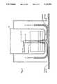
- FIG. 1is a top elevational view of preferred embodiment of the present invention that is an atmospheric pressure chemical vapor deposition (APCVD) system. For clarity the system enclosure is shown only as a dashed outline;
- APCVDatmospheric pressure chemical vapor deposition
- FIG. 2is a cross-sectional view of the system of FIG. 1 taken along the line 2--2 in FIG. 1.
- the system enclosureis shown only as a dashed outline, and the bypass chambers are not shown so that the muffle can be illustrated clearly;
- FIG. 3is a cross-sectional view of the main reaction chamber of the APCVD system of FIG. 1;
- FIG. 4is a diagram of an exemplary source chemical delivery system for supplying source chemicals to the APCVD system of FIG. 1.
- FIGS. 1 and 2illustrate a preferred embodiment of the present invention that is an atmospheric pressure chemical vapor deposition (APCVD) system, referred to by the general reference numeral 10, comprising a conveyor belt 12, a drive system 13, a load station 14, an unload station 16, a muffle 17, a plurality of nitrogen purge curtains 18, an inner bypass isolation chamber 20, an outer bypass isolation chamber 22, a plurality of bypass chamber vents 24, a plurality of heaters 26, a pre-process chamber 28, a main reaction chamber 30, a post-process chamber 32, and a system enclosure 34 (shown with dashed lines so that the other elements can be pictured here).
- APCVDatmospheric pressure chemical vapor deposition
- a substrateis placed on conveyor belt 12 at load station 14.
- the substrateis typically comprised of glass, but other materials are also practical.
- Conveyor belt 12is continuously moving from station 14 to station 16 by virtue of drive system 13.
- belt 12moves about 380 mm/minute.
- As the substrateis drawn into muffle 17 it passes one of the nitrogen purge curtains 18 that isolate the gas atmospheres.
- As the substrate enters enclosure 34it becomes heated to approximately 500° C. by heaters 26.
- Outer bypass isolation chamber 22draws excess gasses through bypass chamber vents 24.
- the next curtain 18seals the entrance to pre-process chamber 28 where a SiO 2 coating may be applied to the substrate.
- a SiO 2 coatingis necessary as a diffusion barrier to highly mobile sodium atoms that exist in soda-lime glass, such as ordinary window glass.
- Sodiumcan poison the electrical conductivity of any film that may be laid down in later steps. Even if the substrate is low in sodium, or has no sodium at all, it may nevertheless be advantageous to lay down a pre-coat of SiO 2 to improve the surface finish and optical properties of the glass substrate.
- Two more nitrogen purge curtains 18isolate chambers 28 and 30. The discussion below relating to FIG. 3 details how the indium-tin-oxide with fluorine (ITO:F) coating is applied to the substrate in main reaction chamber 30.
- Two more nitrogen purge curtains 18isolate chambers 30 and 32.
- Post-process chamber 32can be an additional ITO:F chamber to lay down thicker, more conductive films than is possible with just the single main reaction chamber 30.
- the substratethen exits past two more nitrogen purge curtains 18 and cools down as it reaches unload station 16.
- the indium chemicalis abbreviated “IC” and preferably comprises either trimethylindium-diethyletherate or trimethylindium.
- ICtrimethylindium
- the trimethylindiumis commercially and readily available and is slightly more costly than the trimethylrndium-diethyletherate.
- TCtetramethyltin
- the fluorine chemicalis abbreviated "FC” and comprises bromotrifluoromethane, which is also known as CF 3 Br, and is sold commercially as FREON 13B1.
- the oxygen sourceis preferably water vapor or pure oxygen (O 2 ), and the best results have been obtained when using oxygen.
- the chemicals and methods described hereallow the source chemical delivery system to be operated at temperatures under 200° C.
- FIG. 3details main reaction chamber 30 in system 10. If gas IC is simply exposed to air a useless white powder will be formed. It is crucial in a continuous APCVD process to control the introduction of IC and oxygen to each other and to the surface of a substrate to be coated.
- Reaction chamber 30comprises an injector 50 that establishes a laminar gas flow 52 over the surface of the substrate.
- a relatively inert vapor phase TC and nitrogen mixtureseparates the highly reactive vapor phase IC from the oxygen until surface reaction favoring mechanisms begin.
- a chemical input from a source chemical delivery system(described below) supplies IC and FC in their vapor phase through injector 50 to a first gas lamination that is in contact with the heated substrate.
- the vapor phase ICbecomes adsorbed (stuck on the surface of the substrate).
- a second gas lamination of nitrogen (N 2 ) and TCthen controls the rate that oxygen (O 2 ) from a third gas lamination can pass through to react with the adsorbed layer to form the desired film.
- N 2nitrogen
- O 2oxygen
- FIG. 4illustrates a source chemical delivery system (SCDS) 60 able to supply the necessary chemical inputs to APCVD system 10.
- SCDS 60comprises an oxidizer source, a fluorine chemical source, a nitrogen source, rotometers for the above sources, a mass flow controller, a tin chemical bubbler, heated lines, an indium chemical bubbler, a pair of water baths with heaters, and associated valving.
- the arrangement and use of such a chemical delivery systemis considered to be routine and familiar to a person skilled in the art.
- SCDS 60supplies oxygen from an output line 62, TC and nitrogen from an output line 64, and FC and IC from an output line 66.
Landscapes
- Chemical & Material Sciences (AREA)
- Engineering & Computer Science (AREA)
- Materials Engineering (AREA)
- Chemical Kinetics & Catalysis (AREA)
- General Chemical & Material Sciences (AREA)
- Organic Chemistry (AREA)
- Mechanical Engineering (AREA)
- Metallurgy (AREA)
- Geochemistry & Mineralogy (AREA)
- Life Sciences & Earth Sciences (AREA)
- Physics & Mathematics (AREA)
- Plasma & Fusion (AREA)
- Chemical Vapour Deposition (AREA)
- Manufacturing Of Electric Cables (AREA)
Abstract
Description
2In(CH.sub.3).sub.3 O(C.sub.2 H.sub.5).sub.2 +24O.sub.2 →In.sub.2 O.sub.3 +14CO.sub.2 +19H.sub.2 O (1)
(2-x)In(CH.sub.3).sub.3 O(C.sub.2 H.sub.5).sub.2 +xSn(CH.sub.3).sub.4 +(24-17x/4)O.sub.2 →2In.sub.2-x Sn.sub.x O.sub.3 +(14-3x)CO.sub.2 +(19-7x/2)H.sub.2 O (2)
2In(CH.sub.3).sub.3 O(C.sub.2 H.sub.5).sub.2 +(y/3)CF.sub.3 Br+(24-y/4)O.sub.2 →In.sub.2 O.sub.3-y F.sub.y +(14+y/3)CO.sub.2 +(19-y/6)H.sub.2 O+(y/3)HBr (3)
(2-x)In(CH.sub.3).sub.3 O(C.sub.2 H.sub.5).sub.2 +xSn(CH.sub.3).sub.4 +(y/3)CF.sub.3 Br+(24-17x/4-y/4)O.sub.2 →In.sub.2-x Sn.sub.x O.sub.3-y Fy+(14-3x+y/3)CO.sub.2 +(19-7x/2-y/6)H.sub.2 O+(y/3)HBr(4)
Claims (8)
Priority Applications (4)
| Application Number | Priority Date | Filing Date | Title |
|---|---|---|---|
| US07/668,858US5122391A (en) | 1991-03-13 | 1991-03-13 | Method for producing highly conductive and transparent films of tin and fluorine doped indium oxide by APCVD |
| EP92103329AEP0503382A1 (en) | 1991-03-13 | 1992-02-27 | Method and apparatus for producing highly conductive and transparent films of tin and fluorine doped indium oxide by APCVD |
| JP4053519AJPH04337077A (en) | 1991-03-13 | 1992-03-12 | Method and device for manufacturing high conductive transparent film of indium oxide, to which tin and fluorine are doped, by apcvd |
| KR1019920004058AKR920017802A (en) | 1991-03-13 | 1992-03-12 | Method and apparatus for manufacturing a highly conductive transparent film of indium oxide doped with tin and fluorine by APCVD |
Applications Claiming Priority (1)
| Application Number | Priority Date | Filing Date | Title |
|---|---|---|---|
| US07/668,858US5122391A (en) | 1991-03-13 | 1991-03-13 | Method for producing highly conductive and transparent films of tin and fluorine doped indium oxide by APCVD |
Publications (1)
| Publication Number | Publication Date |
|---|---|
| US5122391Atrue US5122391A (en) | 1992-06-16 |
Family
ID=24684022
Family Applications (1)
| Application Number | Title | Priority Date | Filing Date |
|---|---|---|---|
| US07/668,858Expired - LifetimeUS5122391A (en) | 1991-03-13 | 1991-03-13 | Method for producing highly conductive and transparent films of tin and fluorine doped indium oxide by APCVD |
Country Status (4)
| Country | Link |
|---|---|
| US (1) | US5122391A (en) |
| EP (1) | EP0503382A1 (en) |
| JP (1) | JPH04337077A (en) |
| KR (1) | KR920017802A (en) |
Cited By (58)
| Publication number | Priority date | Publication date | Assignee | Title |
|---|---|---|---|---|
| US5393563A (en)* | 1991-10-29 | 1995-02-28 | Ellis, Jr.; Frank B. | Formation of tin oxide films on glass substrates |
| US5413671A (en)* | 1993-08-09 | 1995-05-09 | Advanced Micro Devices, Inc. | Apparatus and method for removing deposits from an APCVD system |
| US5487783A (en)* | 1994-04-14 | 1996-01-30 | International Business Machines Corporation | Method and apparatus for preventing rupture and contamination of an ultra-clean APCVD reactor during shutdown |
| EP0611733A3 (en)* | 1993-02-16 | 1997-05-07 | Ppg Industries Inc | Apparatus and method for coating glass, compounds and compositions for coating glass and coated glass substrates. |
| KR970048923A (en)* | 1995-12-22 | 1997-07-29 | 김주용 | Method for manufacturing selective oxide mask of semiconductor device |
| US5776236A (en)* | 1993-02-16 | 1998-07-07 | Ppg Industries, Inc. | Mixed metal oxide film having an accelerant |
| US5863337A (en)* | 1993-02-16 | 1999-01-26 | Ppg Industries, Inc. | Apparatus for coating a moving glass substrate |
| US5873388A (en)* | 1996-06-07 | 1999-02-23 | Atmi Ecosys Corporation | System for stabilization of pressure perturbations from oxidation systems for treatment of process gases from semiconductor manufacturing operations |
| US5944900A (en)* | 1997-02-13 | 1999-08-31 | Watkins Johnson Company | Protective gas shield for chemical vapor deposition apparatus |
| US6200389B1 (en) | 1994-07-18 | 2001-03-13 | Silicon Valley Group Thermal Systems Llc | Single body injector and deposition chamber |
| US6241823B1 (en)* | 1998-05-29 | 2001-06-05 | Angewandte Solarenergie Ase Gmbh | Array and method for coating of objects |
| WO2002093628A1 (en)* | 2001-05-17 | 2002-11-21 | Shapiro Nathan P | Continuous processing chamber |
| US20030113451A1 (en)* | 2001-11-01 | 2003-06-19 | Mayer Bruce Edwin | System and method for preferential chemical vapor deposition |
| US6748264B2 (en) | 2002-02-04 | 2004-06-08 | Fook Tin Technologies Limited | Body fat analyzer with integral analog measurement electrodes |
| US6859617B2 (en) | 2000-08-17 | 2005-02-22 | Thermo Stone Usa, Llc | Porous thin film heater and method |
| US20050051090A1 (en)* | 2002-03-29 | 2005-03-10 | Cheon-Soo Cho | Surface treatment system and method |
| KR100521997B1 (en)* | 2003-11-11 | 2005-10-17 | 참이앤티 주식회사 | System for making thin film |
| US20060104879A1 (en)* | 2004-11-12 | 2006-05-18 | Applied Materials, Inc. | Reactor design to reduce particle deposition during process abatement |
| US20070169889A1 (en)* | 2005-10-31 | 2007-07-26 | Clark Daniel O | Methods and apparatus for selectively coupling process tools to abatement reactors |
| US20090010816A1 (en)* | 2003-12-19 | 2009-01-08 | Applied Materials, Inc. | Apparatus and method for controlled combustion of gaseous pollutants |
| US20090081885A1 (en)* | 2007-09-26 | 2009-03-26 | Levy David H | Deposition system for thin film formation |
| US20090117371A1 (en)* | 2006-04-07 | 2009-05-07 | Interpane Entwicklungs-Und Beratungsgesellschaft Mbh & Co. Kg | Weather-resistant layer system |
| US20090130858A1 (en)* | 2007-01-08 | 2009-05-21 | Levy David H | Deposition system and method using a delivery head separated from a substrate by gas pressure |
| US20090165715A1 (en)* | 2007-12-27 | 2009-07-02 | Oh Jae-Eung | Vapor deposition reactor |
| US20090186191A1 (en)* | 2008-01-19 | 2009-07-23 | Peter Lechner | Method of making a transparent metal oxide coated glass panel for photovoltaic module |
| US20100041213A1 (en)* | 2008-08-13 | 2010-02-18 | Synos Technology, Inc. | Vapor Deposition Reactor For Forming Thin Film |
| US20100037820A1 (en)* | 2008-08-13 | 2010-02-18 | Synos Technology, Inc. | Vapor Deposition Reactor |
| US20100092668A1 (en)* | 2008-10-10 | 2010-04-15 | Alta Devices, Inc. | Concentric Showerhead For Vapor Deposition |
| US20100209620A1 (en)* | 2008-05-30 | 2010-08-19 | Alta Devices, Inc. | Method for vapor deposition |
| US20100212591A1 (en)* | 2008-05-30 | 2010-08-26 | Alta Devices, Inc. | Reactor lid assembly for vapor deposition |
| US20100261012A1 (en)* | 2009-04-10 | 2010-10-14 | Jen-Shiun Huang | Flexible Display Panel and Method of Manufacturing the same |
| US20100310771A1 (en)* | 2009-06-08 | 2010-12-09 | Synos Technology, Inc. | Vapor deposition reactor and method for forming thin film |
| US20110076421A1 (en)* | 2009-09-30 | 2011-03-31 | Synos Technology, Inc. | Vapor deposition reactor for forming thin film on curved surface |
| US20110168094A1 (en)* | 2010-01-13 | 2011-07-14 | Honda Motor Co., Ltd. | Plasma film forming apparatus |
| DE102010013038A1 (en)* | 2010-03-26 | 2011-09-29 | Sunfilm Ag | Method for processing substrate for thin film photovoltaic cell, involves arranging electrical conductive layer on surface area, after changing material property in region of substrate, where region abuts on surface area |
| WO2011141516A3 (en)* | 2010-05-11 | 2012-01-26 | Ultra High Vaccum Solutions Ltd. T/A Nines Engineering | Method and apparatus to control surface texture modification of silicon wafers for photovoltaic cell devices |
| US20120055407A1 (en)* | 2009-05-26 | 2012-03-08 | Beneq Oy | Arrangement for processing substrate and substrate carrier |
| WO2012057770A3 (en)* | 2009-10-28 | 2012-06-21 | Alta Devices, Inc. | Reactor clean |
| US20120321786A1 (en)* | 2011-06-17 | 2012-12-20 | Intermolecular, Inc. | System for multi-region processing |
| WO2013019285A2 (en) | 2011-03-23 | 2013-02-07 | Pilkington Group Limited | Apparatus for depositing thin film coatings and method of deposition utilizing such apparatus |
| DE102012204346A1 (en)* | 2012-03-19 | 2013-09-19 | Gebr. Schmid Gmbh | Method for producing a semiconductor wafer doped differently on both sides |
| US20130334089A1 (en)* | 2012-06-15 | 2013-12-19 | Michael P. Remington, Jr. | Glass Container Insulative Coating |
| US20140102368A1 (en)* | 2012-10-12 | 2014-04-17 | Institute Of Nuclear Energy Research Atomic Energy Council, Executive Yuan | Gas isolation chamber and plasma deposition apparatus thereof |
| US8840958B2 (en) | 2011-02-14 | 2014-09-23 | Veeco Ald Inc. | Combined injection module for sequentially injecting source precursor and reactant precursor |
| US20150034008A1 (en)* | 2013-08-02 | 2015-02-05 | Samsung Display Co., Ltd. | Vapor deposition apparatus |
| US9175393B1 (en)* | 2011-08-31 | 2015-11-03 | Alta Devices, Inc. | Tiled showerhead for a semiconductor chemical vapor deposition reactor |
| US9212422B2 (en) | 2011-08-31 | 2015-12-15 | Alta Devices, Inc. | CVD reactor with gas flow virtual walls |
| US9267205B1 (en) | 2012-05-30 | 2016-02-23 | Alta Devices, Inc. | Fastener system for supporting a liner plate in a gas showerhead reactor |
| RU2586956C2 (en)* | 2011-11-22 | 2016-06-10 | Пикосан Ой | Atomic layer deposition reactor for processing batch of substrates and method of processing batch of substrates |
| US20160226031A1 (en)* | 2015-01-29 | 2016-08-04 | Samsung Display Co., Ltd. | Apparatus for manufacturing display apparatus and method of manufacturing display apparatus |
| EP2376397A4 (en)* | 2008-12-23 | 2016-09-28 | Beneq Oy | Glass coating process and apparatus |
| WO2017216065A1 (en)* | 2016-06-13 | 2017-12-21 | Aixtron Se | Device and method for sequentially depositing a multiplicity of layers on substrates, and receiving unit for use in a depositing device |
| US10030307B2 (en)* | 2011-08-01 | 2018-07-24 | Gebr. Schmid Gmbh | Apparatus and process for producing thin layers |
| US10066297B2 (en)* | 2011-08-31 | 2018-09-04 | Alta Devices, Inc. | Tiled showerhead for a semiconductor chemical vapor deposition reactor |
| EP3494246A1 (en)* | 2016-08-04 | 2019-06-12 | Gottfried Wilhelm Leibniz Universität Hannover | Method for surface-coating a component, and coating apparatus for carrying out the method |
| US10400332B2 (en)* | 2017-03-14 | 2019-09-03 | Eastman Kodak Company | Deposition system with interlocking deposition heads |
| US20210355575A1 (en)* | 2018-02-22 | 2021-11-18 | Universal Display Corporation | Modular confined organic print head and system |
| US11584991B2 (en)* | 2015-10-12 | 2023-02-21 | Universal Display Corporation | Apparatus and method for printing multilayer organic thin films from vapor phase in an ultra-pure gas ambient |
Families Citing this family (10)
| Publication number | Priority date | Publication date | Assignee | Title |
|---|---|---|---|---|
| JPH06196419A (en)* | 1992-12-24 | 1994-07-15 | Canon Inc | Chemical vapor deposition apparatus and semiconductor device manufacturing method using the same |
| US5773086A (en)* | 1996-08-13 | 1998-06-30 | Libbey-Owens-Ford Co. | Method of coating flat glass with indium oxide |
| KR20010083628A (en)* | 2000-02-17 | 2001-09-01 | 박종섭 | Belt type cvd apparatus for semiconductor wafer |
| KR20030078454A (en)* | 2002-03-29 | 2003-10-08 | 주식회사 엘지이아이 | Surface treatment device, surface treatment method, surface treated prouct |
| JP4508856B2 (en)* | 2004-12-22 | 2010-07-21 | 三菱重工業株式会社 | Glass substrate deposition equipment |
| JP2009149951A (en)* | 2007-12-21 | 2009-07-09 | Mitsubishi Heavy Ind Ltd | Film thickness adjustment method for film deposition system |
| DE102011077833A1 (en) | 2011-06-20 | 2012-12-20 | Gebr. Schmid Gmbh | Method for processing substrates and apparatus therefor |
| JP5148743B1 (en)* | 2011-12-20 | 2013-02-20 | シャープ株式会社 | Thin film deposition apparatus, thin film deposition method, and thin film solar cell manufacturing method |
| CN103508679B (en)* | 2013-06-04 | 2016-06-15 | 漳州旗滨玻璃有限公司 | A kind of transparent conductive oxide film glass production method and film coating apparatus |
| JP6094513B2 (en)* | 2014-02-28 | 2017-03-15 | 東京エレクトロン株式会社 | Processing gas generator, processing gas generation method, substrate processing method, and storage medium |
Family Cites Families (5)
| Publication number | Priority date | Publication date | Assignee | Title |
|---|---|---|---|---|
| BE560882A (en)* | 1957-09-17 | |||
| US4265974A (en)* | 1976-11-01 | 1981-05-05 | Gordon Roy G | Electrically conductive, infrared reflective, transparent coatings of stannic oxide |
| CA1134214A (en)* | 1978-03-08 | 1982-10-26 | Roy G. Gordon | Deposition method |
| JPH0645888B2 (en)* | 1985-12-17 | 1994-06-15 | キヤノン株式会社 | Deposited film formation method |
| US4834020A (en)* | 1987-12-04 | 1989-05-30 | Watkins-Johnson Company | Atmospheric pressure chemical vapor deposition apparatus |
- 1991
- 1991-03-13USUS07/668,858patent/US5122391A/ennot_activeExpired - Lifetime
- 1992
- 1992-02-27EPEP92103329Apatent/EP0503382A1/ennot_activeCeased
- 1992-03-12JPJP4053519Apatent/JPH04337077A/enactivePending
- 1992-03-12KRKR1019920004058Apatent/KR920017802A/ennot_activeCeased
Non-Patent Citations (4)
| Title |
|---|
| "Thin Films by Conveyorized Atmospheric CVD," presented at the International Society for Hybrid Microelectronics-Internepcon Tech. Sem., Jan. 1983. |
| Gralenski, N. "Advanced APCVD Reactors for Thin Film Deposition," Microelectronic Mfg. & Testing, Sep./Oct., 1987. |
| Gralenski, N. Advanced APCVD Reactors for Thin Film Deposition, Microelectronic Mfg. & Testing, Sep./Oct., 1987.* |
| Thin Films by Conveyorized Atmospheric CVD, presented at the International Society for Hybrid Microelectronics Internepcon Tech. Sem., Jan. 1983.* |
Cited By (93)
| Publication number | Priority date | Publication date | Assignee | Title |
|---|---|---|---|---|
| US5393563A (en)* | 1991-10-29 | 1995-02-28 | Ellis, Jr.; Frank B. | Formation of tin oxide films on glass substrates |
| US5776236A (en)* | 1993-02-16 | 1998-07-07 | Ppg Industries, Inc. | Mixed metal oxide film having an accelerant |
| EP0611733A3 (en)* | 1993-02-16 | 1997-05-07 | Ppg Industries Inc | Apparatus and method for coating glass, compounds and compositions for coating glass and coated glass substrates. |
| US5863337A (en)* | 1993-02-16 | 1999-01-26 | Ppg Industries, Inc. | Apparatus for coating a moving glass substrate |
| US5413671A (en)* | 1993-08-09 | 1995-05-09 | Advanced Micro Devices, Inc. | Apparatus and method for removing deposits from an APCVD system |
| US5487783A (en)* | 1994-04-14 | 1996-01-30 | International Business Machines Corporation | Method and apparatus for preventing rupture and contamination of an ultra-clean APCVD reactor during shutdown |
| US5635242A (en)* | 1994-04-14 | 1997-06-03 | International Business Machines Corporation | Method and apparatus for preventing rupture and contamination of an ultra-clean APCVD reactor during shutdown |
| US6521048B2 (en) | 1994-07-18 | 2003-02-18 | Asml Us, Inc. | Single body injector and deposition chamber |
| US6200389B1 (en) | 1994-07-18 | 2001-03-13 | Silicon Valley Group Thermal Systems Llc | Single body injector and deposition chamber |
| KR970048923A (en)* | 1995-12-22 | 1997-07-29 | 김주용 | Method for manufacturing selective oxide mask of semiconductor device |
| US5873388A (en)* | 1996-06-07 | 1999-02-23 | Atmi Ecosys Corporation | System for stabilization of pressure perturbations from oxidation systems for treatment of process gases from semiconductor manufacturing operations |
| US5944900A (en)* | 1997-02-13 | 1999-08-31 | Watkins Johnson Company | Protective gas shield for chemical vapor deposition apparatus |
| US6241823B1 (en)* | 1998-05-29 | 2001-06-05 | Angewandte Solarenergie Ase Gmbh | Array and method for coating of objects |
| US6859617B2 (en) | 2000-08-17 | 2005-02-22 | Thermo Stone Usa, Llc | Porous thin film heater and method |
| US6626997B2 (en)* | 2001-05-17 | 2003-09-30 | Nathan P. Shapiro | Continuous processing chamber |
| WO2002093628A1 (en)* | 2001-05-17 | 2002-11-21 | Shapiro Nathan P | Continuous processing chamber |
| US20030113451A1 (en)* | 2001-11-01 | 2003-06-19 | Mayer Bruce Edwin | System and method for preferential chemical vapor deposition |
| US20040231588A1 (en)* | 2001-11-01 | 2004-11-25 | Mayer Bruce Edwin | System and method for preferential chemical vapor deposition |
| US6748264B2 (en) | 2002-02-04 | 2004-06-08 | Fook Tin Technologies Limited | Body fat analyzer with integral analog measurement electrodes |
| US20050051090A1 (en)* | 2002-03-29 | 2005-03-10 | Cheon-Soo Cho | Surface treatment system and method |
| US7175880B2 (en)* | 2002-03-29 | 2007-02-13 | Lg Electronics Inc. | Surface treatment system and method |
| KR100521997B1 (en)* | 2003-11-11 | 2005-10-17 | 참이앤티 주식회사 | System for making thin film |
| US20090010816A1 (en)* | 2003-12-19 | 2009-01-08 | Applied Materials, Inc. | Apparatus and method for controlled combustion of gaseous pollutants |
| US7569193B2 (en) | 2003-12-19 | 2009-08-04 | Applied Materials, Inc. | Apparatus and method for controlled combustion of gaseous pollutants |
| US20070274876A1 (en)* | 2004-11-12 | 2007-11-29 | Applied Materials, Inc. | Reactor design to reduce particle deposition during process abatement |
| US20060104879A1 (en)* | 2004-11-12 | 2006-05-18 | Applied Materials, Inc. | Reactor design to reduce particle deposition during process abatement |
| US7736599B2 (en) | 2004-11-12 | 2010-06-15 | Applied Materials, Inc. | Reactor design to reduce particle deposition during process abatement |
| US7985379B2 (en) | 2004-11-12 | 2011-07-26 | Applied Materials, Inc. | Reactor design to reduce particle deposition during process abatement |
| US20070172399A1 (en)* | 2005-10-31 | 2007-07-26 | Clark Daniel O | Methods and apparatus for sensing characteristics of the contents of a process abatement reactor |
| US20070190469A1 (en)* | 2005-10-31 | 2007-08-16 | Clark Daniel O | Methods and apparatus for preventing deposition of reaction products in process abatement reactors |
| US20070172398A1 (en)* | 2005-10-31 | 2007-07-26 | Clark Daniel O | Methods and apparatus for manufacturing a process abatement reactor |
| US20070169889A1 (en)* | 2005-10-31 | 2007-07-26 | Clark Daniel O | Methods and apparatus for selectively coupling process tools to abatement reactors |
| US7700049B2 (en) | 2005-10-31 | 2010-04-20 | Applied Materials, Inc. | Methods and apparatus for sensing characteristics of the contents of a process abatement reactor |
| US7736600B2 (en) | 2005-10-31 | 2010-06-15 | Applied Materials, Inc. | Apparatus for manufacturing a process abatement reactor |
| US20090117371A1 (en)* | 2006-04-07 | 2009-05-07 | Interpane Entwicklungs-Und Beratungsgesellschaft Mbh & Co. Kg | Weather-resistant layer system |
| US20090130858A1 (en)* | 2007-01-08 | 2009-05-21 | Levy David H | Deposition system and method using a delivery head separated from a substrate by gas pressure |
| US11136667B2 (en) | 2007-01-08 | 2021-10-05 | Eastman Kodak Company | Deposition system and method using a delivery head separated from a substrate by gas pressure |
| US10351954B2 (en) | 2007-01-08 | 2019-07-16 | Eastman Kodak Company | Deposition system and method using a delivery head separated from a substrate by gas pressure |
| US20090081885A1 (en)* | 2007-09-26 | 2009-03-26 | Levy David H | Deposition system for thin film formation |
| US8398770B2 (en)* | 2007-09-26 | 2013-03-19 | Eastman Kodak Company | Deposition system for thin film formation |
| US20090165715A1 (en)* | 2007-12-27 | 2009-07-02 | Oh Jae-Eung | Vapor deposition reactor |
| US8333839B2 (en)* | 2007-12-27 | 2012-12-18 | Synos Technology, Inc. | Vapor deposition reactor |
| US20090186191A1 (en)* | 2008-01-19 | 2009-07-23 | Peter Lechner | Method of making a transparent metal oxide coated glass panel for photovoltaic module |
| EP2088132A3 (en)* | 2008-01-19 | 2010-07-07 | SCHOTT Solar AG | Method for manufacturing a glass disc for a photovoltaic module coated with a transparent metal oxide |
| US8852696B2 (en) | 2008-05-30 | 2014-10-07 | Alta Devices, Inc. | Method for vapor deposition |
| US20100212591A1 (en)* | 2008-05-30 | 2010-08-26 | Alta Devices, Inc. | Reactor lid assembly for vapor deposition |
| US20100209620A1 (en)* | 2008-05-30 | 2010-08-19 | Alta Devices, Inc. | Method for vapor deposition |
| US20100037820A1 (en)* | 2008-08-13 | 2010-02-18 | Synos Technology, Inc. | Vapor Deposition Reactor |
| US20100041213A1 (en)* | 2008-08-13 | 2010-02-18 | Synos Technology, Inc. | Vapor Deposition Reactor For Forming Thin Film |
| US8470718B2 (en) | 2008-08-13 | 2013-06-25 | Synos Technology, Inc. | Vapor deposition reactor for forming thin film |
| US20100092668A1 (en)* | 2008-10-10 | 2010-04-15 | Alta Devices, Inc. | Concentric Showerhead For Vapor Deposition |
| US9121096B2 (en) | 2008-10-10 | 2015-09-01 | Alta Devices, Inc. | Concentric showerhead for vapor deposition |
| EP2376397A4 (en)* | 2008-12-23 | 2016-09-28 | Beneq Oy | Glass coating process and apparatus |
| US20100261012A1 (en)* | 2009-04-10 | 2010-10-14 | Jen-Shiun Huang | Flexible Display Panel and Method of Manufacturing the same |
| US20120055407A1 (en)* | 2009-05-26 | 2012-03-08 | Beneq Oy | Arrangement for processing substrate and substrate carrier |
| US20100310771A1 (en)* | 2009-06-08 | 2010-12-09 | Synos Technology, Inc. | Vapor deposition reactor and method for forming thin film |
| US8758512B2 (en) | 2009-06-08 | 2014-06-24 | Veeco Ald Inc. | Vapor deposition reactor and method for forming thin film |
| US20110076421A1 (en)* | 2009-09-30 | 2011-03-31 | Synos Technology, Inc. | Vapor deposition reactor for forming thin film on curved surface |
| WO2012057770A3 (en)* | 2009-10-28 | 2012-06-21 | Alta Devices, Inc. | Reactor clean |
| US9127364B2 (en) | 2009-10-28 | 2015-09-08 | Alta Devices, Inc. | Reactor clean |
| US8573154B2 (en)* | 2010-01-13 | 2013-11-05 | Honda Motor Co., Ltd. | Plasma film forming apparatus |
| US20110168094A1 (en)* | 2010-01-13 | 2011-07-14 | Honda Motor Co., Ltd. | Plasma film forming apparatus |
| DE102010013038B4 (en)* | 2010-03-26 | 2012-01-19 | Schüco Tf Gmbh & Co. Kg | Method for producing a photovoltaic cell |
| DE102010013038A1 (en)* | 2010-03-26 | 2011-09-29 | Sunfilm Ag | Method for processing substrate for thin film photovoltaic cell, involves arranging electrical conductive layer on surface area, after changing material property in region of substrate, where region abuts on surface area |
| US20130069204A1 (en)* | 2010-05-11 | 2013-03-21 | Ultra High Vacuum Solutions Ltd 1/A Nines Engine | Method and Apparatus to Control Surface Texture Modification of Silicon Wafers for Photovoltaic Cell Devices |
| US9548224B2 (en)* | 2010-05-11 | 2017-01-17 | Ultra High Vacuum Solutions Ltd. | Method and apparatus to control surface texture modification of silicon wafers for photovoltaic cell devices |
| WO2011141516A3 (en)* | 2010-05-11 | 2012-01-26 | Ultra High Vaccum Solutions Ltd. T/A Nines Engineering | Method and apparatus to control surface texture modification of silicon wafers for photovoltaic cell devices |
| US8840958B2 (en) | 2011-02-14 | 2014-09-23 | Veeco Ald Inc. | Combined injection module for sequentially injecting source precursor and reactant precursor |
| WO2013019285A2 (en) | 2011-03-23 | 2013-02-07 | Pilkington Group Limited | Apparatus for depositing thin film coatings and method of deposition utilizing such apparatus |
| US9540277B2 (en) | 2011-03-23 | 2017-01-10 | Pilkington Group Limited | Apparatus for depositing thin film coatings and method of deposition utilizing such apparatus |
| US20120321786A1 (en)* | 2011-06-17 | 2012-12-20 | Intermolecular, Inc. | System for multi-region processing |
| US9175392B2 (en)* | 2011-06-17 | 2015-11-03 | Intermolecular, Inc. | System for multi-region processing |
| US10030307B2 (en)* | 2011-08-01 | 2018-07-24 | Gebr. Schmid Gmbh | Apparatus and process for producing thin layers |
| US10066297B2 (en)* | 2011-08-31 | 2018-09-04 | Alta Devices, Inc. | Tiled showerhead for a semiconductor chemical vapor deposition reactor |
| US9212422B2 (en) | 2011-08-31 | 2015-12-15 | Alta Devices, Inc. | CVD reactor with gas flow virtual walls |
| US9175393B1 (en)* | 2011-08-31 | 2015-11-03 | Alta Devices, Inc. | Tiled showerhead for a semiconductor chemical vapor deposition reactor |
| RU2586956C2 (en)* | 2011-11-22 | 2016-06-10 | Пикосан Ой | Atomic layer deposition reactor for processing batch of substrates and method of processing batch of substrates |
| WO2013139663A3 (en)* | 2012-03-19 | 2014-01-09 | Gebr. Schmid Gmbh | Method for producing a semiconductor wafer doped differently on both sides |
| DE102012204346A1 (en)* | 2012-03-19 | 2013-09-19 | Gebr. Schmid Gmbh | Method for producing a semiconductor wafer doped differently on both sides |
| US9267205B1 (en) | 2012-05-30 | 2016-02-23 | Alta Devices, Inc. | Fastener system for supporting a liner plate in a gas showerhead reactor |
| US20130334089A1 (en)* | 2012-06-15 | 2013-12-19 | Michael P. Remington, Jr. | Glass Container Insulative Coating |
| US20140102368A1 (en)* | 2012-10-12 | 2014-04-17 | Institute Of Nuclear Energy Research Atomic Energy Council, Executive Yuan | Gas isolation chamber and plasma deposition apparatus thereof |
| US20150034008A1 (en)* | 2013-08-02 | 2015-02-05 | Samsung Display Co., Ltd. | Vapor deposition apparatus |
| US20160226031A1 (en)* | 2015-01-29 | 2016-08-04 | Samsung Display Co., Ltd. | Apparatus for manufacturing display apparatus and method of manufacturing display apparatus |
| US10573851B2 (en) | 2015-01-29 | 2020-02-25 | Samsung Display Co., Ltd. | Apparatus for manufacturing display apparatus and method of manufacturing display apparatus |
| US12207530B2 (en)* | 2015-01-29 | 2025-01-21 | Samsung Display Co., Ltd. | Apparatus for manufacturing display apparatus and method of manufacturing display apparatus |
| US11584991B2 (en)* | 2015-10-12 | 2023-02-21 | Universal Display Corporation | Apparatus and method for printing multilayer organic thin films from vapor phase in an ultra-pure gas ambient |
| US11976360B2 (en) | 2015-10-12 | 2024-05-07 | Universal Display Corporation | Organic vapor jet printing system |
| WO2017216065A1 (en)* | 2016-06-13 | 2017-12-21 | Aixtron Se | Device and method for sequentially depositing a multiplicity of layers on substrates, and receiving unit for use in a depositing device |
| EP3494246A1 (en)* | 2016-08-04 | 2019-06-12 | Gottfried Wilhelm Leibniz Universität Hannover | Method for surface-coating a component, and coating apparatus for carrying out the method |
| US10400332B2 (en)* | 2017-03-14 | 2019-09-03 | Eastman Kodak Company | Deposition system with interlocking deposition heads |
| US20210355575A1 (en)* | 2018-02-22 | 2021-11-18 | Universal Display Corporation | Modular confined organic print head and system |
| US11746408B2 (en)* | 2018-02-22 | 2023-09-05 | Universal Display Corporation | Modular confined organic print head and system |
Also Published As
| Publication number | Publication date |
|---|---|
| EP0503382A1 (en) | 1992-09-16 |
| KR920017802A (en) | 1992-10-21 |
| JPH04337077A (en) | 1992-11-25 |
Similar Documents
| Publication | Publication Date | Title |
|---|---|---|
| US5122391A (en) | Method for producing highly conductive and transparent films of tin and fluorine doped indium oxide by APCVD | |
| US4146657A (en) | Method of depositing electrically conductive, infra-red reflective, transparent coatings of stannic oxide | |
| KR100577945B1 (en) | Method for Forming Tin Oxide Coating on Glass | |
| US4265974A (en) | Electrically conductive, infrared reflective, transparent coatings of stannic oxide | |
| USRE31708E (en) | Method of depositing electrically conductive, infra-red reflective, transparent coatings of stannic oxide | |
| FI64128C (en) | FOERFARANDE FOER PAOFOERING AV EN TRANSPARENT FLUORDOPAD STANNIOXIDFILM PAO ETT UPPHETTAT SUBSTRAT MED REGLERAD FLUORFOERORENINGSHALT | |
| US4393095A (en) | Chemical vapor deposition of vanadium oxide coatings | |
| US3949146A (en) | Process for depositing transparent electrically conductive tin oxide coatings on a substrate | |
| RU2447030C2 (en) | Method of making glass article with doped zinc oxide coating, having low resistivity, and coated glass article made using said method | |
| KR20030092075A (en) | Chemical Vapor Deposition of Antimony-Doped Metal Oxide | |
| US4400412A (en) | Thermochromic vanadium oxide coated glass | |
| EP0463079A4 (en) | Zinc oxyfluoride transparent conductor | |
| US5773086A (en) | Method of coating flat glass with indium oxide | |
| US3457106A (en) | Metal-tungsten bronze films | |
| US8163404B2 (en) | Chlorine, fluorine and lithium co-doped transparent conductive films and methods for fabricating the same | |
| CN112209627A (en) | Glass substrate with film and method for producing same | |
| JPH04214047A (en) | Method for forming silicon oxycarbide layer on glass support and product containing semiconductor layer | |
| CN1204067C (en) | Method for on-line producing low radiation film glass by floating process | |
| JPH0686655B2 (en) | Method for manufacturing composite conductive layer | |
| JP3406693B2 (en) | Method for forming tin (IV) oxide film | |
| JPH07330336A (en) | Method for forming tin (IV) oxide film | |
| JPS63170813A (en) | Method for forming transparent conductive film | |
| JPS63241805A (en) | Transparent conducting film and manufacture thereof | |
| CN116395981A (en) | Glass substrate with transparent conductive film and manufacturing method thereof | |
| MXPA98002841A (en) | Coating of glass |
Legal Events
| Date | Code | Title | Description |
|---|---|---|---|
| AS | Assignment | Owner name:WATKINS-JOHNSON COMPANY, 3333 HILLVIEW AVENUE, PAL Free format text:ASSIGNMENT OF ASSIGNORS INTEREST.;ASSIGNOR:MAYER, BRUCE E.;REEL/FRAME:005644/0528 Effective date:19910311 | |
| STCF | Information on status: patent grant | Free format text:PATENTED CASE | |
| FEPP | Fee payment procedure | Free format text:PAYOR NUMBER ASSIGNED (ORIGINAL EVENT CODE: ASPN); ENTITY STATUS OF PATENT OWNER: SMALL ENTITY | |
| FPAY | Fee payment | Year of fee payment:4 | |
| AS | Assignment | Owner name:FIRST UNION COMMERCIAL CORPORATION, VIRGINIA Free format text:SECURITY AGREEMENT;ASSIGNORS:TSMD ACQUISITION CORP.;STELLEX MICROWAVE SYSTEMS, INC.;REEL/FRAME:009556/0267 Effective date:19980529 | |
| AS | Assignment | Owner name:WJ SEMICONDUCTOR EQUIPMENT GROUP, INC., CALIFORNIA Free format text:ASSIGNMENT OF ASSIGNORS INTEREST;ASSIGNOR:WATKINS-JOHNSON COMPANY;REEL/FRAME:009912/0070 Effective date:19990426 | |
| AS | Assignment | Owner name:SEMICONDUCTOR EQUIPMENT GROUP, LLC, CALIFORNIA Free format text:ASSIGNMENT OF ASSIGNORS INTEREST;ASSIGNOR:WJ SEMICONUCTOR EQUIPMENT GROUP, INC.;REEL/FRAME:009968/0765 Effective date:19990603 | |
| AS | Assignment | Owner name:SILICON VALLEY GROUP, THERMAL SYSTEMS LLC, CALIFOR Free format text:ASSIGNMENT OF ASSIGNORS INTEREST;ASSIGNOR:SEMICONDUCTOR EQUIPMENT GROUP, LLC;REEL/FRAME:010263/0951 Effective date:19991006 | |
| AS | Assignment | Owner name:FIRST UNION COMMERICIAL CORPORATION, VIRGINIA Free format text:RELINQUISHMENT AND AMENDMENT TO AMENDED AND RESTATED PATENT SECURITY AGREEMENT;ASSIGNORS:TSMD ACQUISITION CORPORATION;STELLEX MICROWAVE SYSTEMS, INC.;REEL/FRAME:010310/0553;SIGNING DATES FROM 19990329 TO 19990330 | |
| FPAY | Fee payment | Year of fee payment:8 | |
| CC | Certificate of correction | ||
| FEPP | Fee payment procedure | Free format text:PAT HOLDER CLAIMS SMALL ENTITY STATUS, ENTITY STATUS SET TO SMALL (ORIGINAL EVENT CODE: LTOS); ENTITY STATUS OF PATENT OWNER: SMALL ENTITY | |
| FPAY | Fee payment | Year of fee payment:12 | |
| REMI | Maintenance fee reminder mailed | ||
| AS | Assignment | Owner name:UNITED COMMERCIAL BANK, CALIFORNIA Free format text:INTELLECTUAL PROPERTY SECURITY AGREEMENT;ASSIGNORS:AVIZA TECHNOLOGY, INC.;AVIZA, INC.;REEL/FRAME:019265/0381 Effective date:20070413 | |
| AS | Assignment | Owner name:SILICON VALLEY GROUP, INC., CALIFORNIA Free format text:MERGER;ASSIGNOR:SILICON VALLEY GROUP, THERMAL SYSTEMS LLC;REEL/FRAME:019899/0516 Effective date:20001229 | |
| AS | Assignment | Owner name:ASML US, INC., CALIFORNIA Free format text:MERGER/CHANGE OF NAME;ASSIGNOR:SILICON VALLEY GROUP, INC.;REEL/FRAME:019899/0758 Effective date:20011101 Owner name:AVIZA TECHNOLOGY, INC., CALIFORNIA Free format text:MERGER;ASSIGNOR:THERMAL ACQUISITION CORP.;REEL/FRAME:019910/0076 Effective date:20031015 Owner name:THERMAL ACQUISITION CORP., CALIFORNIA Free format text:MERGER;ASSIGNOR:ASML US, INC.;REEL/FRAME:019899/0814 Effective date:20031010 |