US5118975A - Digital clock buffer circuit providing controllable delay - Google Patents
Digital clock buffer circuit providing controllable delayDownload PDFInfo
- Publication number
- US5118975A US5118975AUS07/489,079US48907990AUS5118975AUS 5118975 AUS5118975 AUS 5118975AUS 48907990 AUS48907990 AUS 48907990AUS 5118975 AUS5118975 AUS 5118975A
- Authority
- US
- United States
- Prior art keywords
- signal
- delay
- signals
- response
- circuit
- Prior art date
- Legal status (The legal status is an assumption and is not a legal conclusion. Google has not performed a legal analysis and makes no representation as to the accuracy of the status listed.)
- Expired - Lifetime
Links
Images


Classifications
- G—PHYSICS
- G06—COMPUTING OR CALCULATING; COUNTING
- G06F—ELECTRIC DIGITAL DATA PROCESSING
- G06F1/00—Details not covered by groups G06F3/00 - G06F13/00 and G06F21/00
- G06F1/04—Generating or distributing clock signals or signals derived directly therefrom
- G06F1/10—Distribution of clock signals, e.g. skew
- H—ELECTRICITY
- H03—ELECTRONIC CIRCUITRY
- H03L—AUTOMATIC CONTROL, STARTING, SYNCHRONISATION OR STABILISATION OF GENERATORS OF ELECTRONIC OSCILLATIONS OR PULSES
- H03L7/00—Automatic control of frequency or phase; Synchronisation
- H03L7/06—Automatic control of frequency or phase; Synchronisation using a reference signal applied to a frequency- or phase-locked loop
- H03L7/08—Details of the phase-locked loop
- H03L7/081—Details of the phase-locked loop provided with an additional controlled phase shifter
- H03L7/0812—Details of the phase-locked loop provided with an additional controlled phase shifter and where no voltage or current controlled oscillator is used
- H03L7/0814—Details of the phase-locked loop provided with an additional controlled phase shifter and where no voltage or current controlled oscillator is used the phase shifting device being digitally controlled
- H—ELECTRICITY
- H03—ELECTRONIC CIRCUITRY
- H03L—AUTOMATIC CONTROL, STARTING, SYNCHRONISATION OR STABILISATION OF GENERATORS OF ELECTRONIC OSCILLATIONS OR PULSES
- H03L7/00—Automatic control of frequency or phase; Synchronisation
- H03L7/06—Automatic control of frequency or phase; Synchronisation using a reference signal applied to a frequency- or phase-locked loop
- H03L7/08—Details of the phase-locked loop
- H03L7/081—Details of the phase-locked loop provided with an additional controlled phase shifter
- H03L7/0812—Details of the phase-locked loop provided with an additional controlled phase shifter and where no voltage or current controlled oscillator is used
- H03L7/0816—Details of the phase-locked loop provided with an additional controlled phase shifter and where no voltage or current controlled oscillator is used the controlled phase shifter and the frequency- or phase-detection arrangement being connected to a common input
- H—ELECTRICITY
- H03—ELECTRONIC CIRCUITRY
- H03L—AUTOMATIC CONTROL, STARTING, SYNCHRONISATION OR STABILISATION OF GENERATORS OF ELECTRONIC OSCILLATIONS OR PULSES
- H03L7/00—Automatic control of frequency or phase; Synchronisation
- H03L7/06—Automatic control of frequency or phase; Synchronisation using a reference signal applied to a frequency- or phase-locked loop
- H03L7/08—Details of the phase-locked loop
- H03L7/085—Details of the phase-locked loop concerning mainly the frequency- or phase-detection arrangement including the filtering or amplification of its output signal
- H03L7/087—Details of the phase-locked loop concerning mainly the frequency- or phase-detection arrangement including the filtering or amplification of its output signal using at least two phase detectors or a frequency and phase detector in the loop
- H—ELECTRICITY
- H03—ELECTRONIC CIRCUITRY
- H03L—AUTOMATIC CONTROL, STARTING, SYNCHRONISATION OR STABILISATION OF GENERATORS OF ELECTRONIC OSCILLATIONS OR PULSES
- H03L7/00—Automatic control of frequency or phase; Synchronisation
- H03L7/06—Automatic control of frequency or phase; Synchronisation using a reference signal applied to a frequency- or phase-locked loop
- H03L7/08—Details of the phase-locked loop
- H03L7/085—Details of the phase-locked loop concerning mainly the frequency- or phase-detection arrangement including the filtering or amplification of its output signal
- H03L7/089—Details of the phase-locked loop concerning mainly the frequency- or phase-detection arrangement including the filtering or amplification of its output signal the phase or frequency detector generating up-down pulses
Definitions
- the inventionrelates generally to the field of digital circuitry, and more specifically to clock buffer control circuits for controlling relative timing of sequential ticks of a clock signal used to control the digital circuitry.
- Digital systemsnormally operate in synchronism with sequential ticks of one or more clock signals.
- the ticks of a clock signalwhich are defined by voltage transitions representing its leading or trailing edges, control processing circuitry that decodes, processes and stores data signals in response to control signals, in a sequence of processing cycles.
- the rate at which a digital system can process datais determined, in part, by the maximum amount of time required for the data and control signals to propagate through the processing circuitry in one processing cycle.
- Typical digital circuitryis comprised of a number of integrated circuit chips which contain much of the processing circuitry. Many of the chips have one or more clock terminals, each terminal receiving a clock signal that controls the circuitry on the chip. Typically, a clock terminal on a chip is connected to a clock buffer circuit that drives a network of lines on the chip used to distribute the clock signal to the processing circuitry thereon.
- the edges of the clock signalare delayed, such that the edges of the clock signal at the output of the clock buffer circuit do not occur in precise synchronism with the edges of the clock signal at the clock terminal. While this might not be a major problem if the propagation delay were uniform in all of the chips that are used in a system, in fact the propagation delay from chip to chip may vary unpredictably by a substantial amount as a result of variations in manufacturing from chip to chip. To accommodate such unpredictable variations, the clock period has to be further increased (otherwise stated, the time between edges has to be further increased), which reduces the rate at which processing can be accomplished by the system. Alternately, chips can be tested and selected for use in a system if they meet selected criteria in the uniformity of the propagation delay exhibited thereby, but that would result in a likely increase in the cost of the system.
- the inventionprovides a new and improved clock buffer circuit for use in connection with, for example, an integrated circuit chip, that controls the timing of ticks in the clock signal as transmitted thereby in relation to the transitions in a system clocking signal received thereby.
- the clock buffer circuitgenerates a local clock signal in response to a system clock signal.
- the clock buffer circuitincludes a buffer circuit for generating said local clock signal in response to an intermediate clock signal.
- a buffer control circuitgenerates the intermediate clock signal in response to said system clock signal and the local clock signal.
- the buffer control circuitprovides a variable delay so that, with an additional delay provided by the buffer circuit, the local clock signal has a selected phase relationship in relation to the system clock signal.
- the clock buffer circuitcontrols the relative phases of the local clock signal in relation to the system clock signal. If the circuit is implemented on an integrated circuit chip, for example, it can obviate problems that may result from timing differences among chips which may result from tolerances and variations in manufacturing processes. This can reduce manufacturing costs that might normally be imposed by tight manufacturing tolerances or that might be required to screen chips after manufacture. Alternately, the clock buffer circuit can enable a corresponding increase in processing by the processing circuitry on the chip, since variations in the timings of the local clock signal among the various chips comprising a system can be controlled or reduced.
- FIG. 1depicts a functional block diagram of a clock buffer circuit constructed in accordance with the invention
- FIG. 2depicts a functional block diagram of a voltage controlled delay element and delay control element useful in the clock buffer circuit depicted in FIG. 1;
- FIG. 4is a logic diagram of a clock delay select circuit useful in the voltage controlled delay element depicted in FIG. 2;
- FIG. 5is a state diagram useful in understanding the operations of the delay control element depicted in FIGS. 1 and 2;
- FIG. 6is a logic diagram of a phase comparator useful in the clock buffer circuit depicted in FIG. 1.
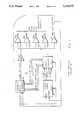
- FIG. 1depicts a functional block diagram of a clock buffer circuit 10 constructed in accordance with the invention.
- the clock buffer circuit 10includes a buffer 11 and a buffer control circuit 12, all of which may be located on a single integrated circuit chip.
- the clock buffer circuit 10receives a periodic SYS CLK IN system clock in signal, which may be generated by a clock circuit (not shown) which may be external to the chip containing clock buffer circuit 10, and in response thereto generates one or more DEL CLK OUT delayed clock out signals which are transmitted to other circuitry on the chip (not shown).
- the SYS CLK IN system clock in signalhas a substantially constant period, that is, the time periods between the transitions defining successive leading edges of the signal are substantially uniform, and the time periods between the transitions defining successive trailing edges of the signal are also substantially uniform.
- the time periods between successive edges of the SYS CLK IN system clock in signalmay also be substantially uniform, in which case the signal is said to have a "fifty-percent duty cycle.”
- the clock buffer circuit 10generates the DEL CLK OUT delayed clock out signals to have substantially the same timing characteristics as the SYS CLK IN system clock in signal. That is, the clock buffer circuit 10 generates the DEL CLK OUT delayed clock out signals to have substantially the same periods between successive leading edges and successive trailing edges as the SYS CLK IN system clock in signal. In addition the clock buffer circuit generates the DEL CLK OUT delayed clock out signals to have the same timing relationships between successive edges as the SYS CLK IN system clock in signal, with the result that all of the signals have the same duty cycle.
- the clock buffer circuit 10also generates the DEL CLK OUT delayed clock out signals so that their transitions have a predetermined and controllable timing relationship with the corresponding transitions of the SYS CLK IN system clock in signal. That is, (1) the transitions of the DEL CLK OUT signals defining their leading edges all lead or lag the transitions defining the leading edges of the SYS CLK IN system clock in signal by a uniform, predetermined, and controllable amount, and (2) the transitions defining the trailing edges of the DEL CLK OUT delayed clock out signal have the same relationship with the transitions defining the trailing edge of the SYS CLK IN system clock in signal.
- the transitions of the DEL CLK OUT signals defining their leading edgesall lead or lag the transitions defining the leading edges of the SYS CLK IN system clock in signal by a uniform, predetermined, and controllable amount
- the transitions defining the trailing edges of the DEL CLK OUT delayed clock out signalhave the same relationship with the transitions defining the trailing edge
- the clock buffer circuitgenerates the DEL CLK OUT delayed clock out signals so that their leading edges occur at substantially the same time as the leading edges of the SYS CLK IN system clock in signal and their trailing edges also occur at substantially the same time as the trailing edges of the SYS CLK IN system clock in signal.
- the clock buffer circuit 10since the SYS CLK IN system clock in signal has a substantially uniform periodicity, the clock buffer circuit 10 essentially provides DEL CLK OUT delayed clock out signals with an effective zero delay from the SYS CLK IN system clock in signal.
- the buffer 11includes a buffer amplifier 13 which receives a COMP DEL CLK composite delayed clock signal generated by the buffer control circuit 12, and, in turn, drives one or more drivers 14A through 14N (generally identified by reference numeral 13.
- the drivers 14A through 14Ngenerate one or more DEL CLK OUT delayed clock out signals that are transmitted over lines 15A through 15N (generally identified by reference numeral 14), representing a clock network, to control operations of processing circuits (not shown).
- the drivers 14A through 14N on a chipwill have substantially the same operational characteristics, so that transitions in the DEL CLK OUT delayed clock out signals generated by the various drivers 14A through 14N occur substantially simultaneously.
- the buffer amplifier 13drives another driver 16 which generates a DEL CLK OUT REF delayed clock out reference signal, which will be used as described below.
- the driver 16also has the substantially same operational characteristics as the drivers 14.
- the DEL CLK OUT delayed clock out signals from drivers 14have substantially the same timing characteristics as the DEL CLK OUT REF delayed clock out reference signal generated by driver 16.
- the transitions of the DEL CLK OUT REF delayed clock out reference signaloccur substantially simultaneously with the transitions of the DEL CLK OUT delayed clock out signals generated by drivers 14.
- the buffer control circuit 12receives the SYS CLK IN system clock in signal and generates the COMP DEL CLK composite delayed clock signal in response to both the SYS CLK IN system clock in signal and the DEL CLK OUT REF delayed clock out reference signal from driver 16.
- the buffer control circuit 12generates the COMP DEL CLK composite delayed clock signal so as to have transitions that occur at times so that the transitions of the DEL CLK OUT REF delayed clock out reference signal, and thus the transitions of the DEL CLK OUT delayed clock out signals, occur at substantially the same time as transitions of the SYS CLK IN system clock in signal, thereby providing the effective zero delay through the clock buffer 10. Otherwise stated, the buffer control circuit 12 provides a delay that, with the additional delay provided by the buffer 11, results in DEL CLK OUT delayed clock out signals that have an effective zero delay in relation to the SYS CLK IN system clock in signal.
- the buffer control circuit 12includes a variable delay element 20 that receives the SYS CLK IN system clock in signal, and generates the COMP DEL CLK composite delayed clock signal with a delay that is controllable in response to delay control signals which it receives over a delay control bus 21 from a delay control circuit 22.
- a phase comparator 23receives the SYS CLK IN system clock in signal and the DEL CLK OUT REF delayed clock out reference signal from driver 16 and generates, in response thereto, a LEAD signal, a LAG signal, a PH OK in-phase signal, and a PH BAD out-of-phase signal, which the delay control circuit 22 use in controlling the variable delay element 20.
- the signals generated by the phase comparator 23indicate selected timing relationships between the SYS CLK IN system clock in signal and the DEL CLK OUT REF delayed clock out reference signal.
- the LEAD signalwhen asserted, indicates that the edges of the SYS CLK IN system clock in signal lead corresponding edges of the DEL CLK OUT REF delayed clock out reference signal.
- the LAG signalwhen asserted, indicates that the edges of the SYS CLK IN system clock in signal lag corresponding edges of the DEL CLK OUT REF delayed clock out reference signal.
- the PH OK in-phase signalwhen asserted, indicates that the edges of the SYS CLK IN system clock in signal occur substantially simultaneously with corresponding edges of the DEL CLK OUT REF delayed clock out reference signal, in which case the signals are in phase.
- the PH OUT out-of-phase signalwhen asserted, indicates that the edges of the SYS CLK IN system clock in signal occur substantially simultaneously with opposite edges of the DEL CLK OUT REF delayed clock out reference signal, that is, the SYS CLK IN system clock in signal and the DEL CLK OUT REF delayed clock out reference signal are approximately one hundred and eighty degrees out of phase.
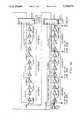
- variable delay element 20 and delay control circuit 22will be described in greater detail in connection with FIG. 2.
- the variable delay element 20includes two delay paths identified here as A delay path 25A and B delay path 25B (generally identified by reference numeral 25).
- Each delay path 25provides an amount of delay, which can be incrementally varied independent of the other path by the delay control circuit 22.
- the delay control circuit 22alternately switches between the A and B delay paths 25A and 25B as it varies the delay provided by the variable delay element 20.
- the A delay path 25Aincludes a shared delay line 30, which is shared between the two delay path 25 and an A delay line 26A.
- the shared delay linereceives the SYS CLK IN system clock in signal and the A delay line 26A generates an A DEL CLK delayed clock signal which is delayed from the SYS CLK IN system clock in signal by an amount determined by a binary counter 27A.
- the binary counter 27Ais controlled by A UP count up and A DN count down signals which it receives from the delay control circuit 22 over delay control bus 21.
- the delay control circuit 22When the delay control circuit 22 asserts the A UP count up or the A DN count down signal, the counter counts up or down, respectively.
- the A delay path 25Aincluding the A delay line 26A, the counter 27A, and the shared delay line 30, will be described in greater detail below in connection with FIGS. 3A through 3C.
- the counter 27Agenerates binary-encoded AC(8:0) counter output signals coupled to the A delay line 26A to control the amount of delay provided thereby.
- the counter 27Awhen the counter 27A counts beyond either the upper or the lower end of its range, such that the binary-encoded value of the AC(8:0) counter output signals equals zero, it asserts an A WRAP signal, which is transmitted to the delay control circuit 22 over the delay status bus 24.
- the delay control circuit 22asserts an A LD load enabling signal which enables the counter to load an initialization value in the mid-point of its range.
- the counter 27Aprovides a sufficient range of values for the AC(8:0) counter output signals so that the amount delay provided by the A delay path 25A can vary over several periods of the SYS CLK IN system clock in signal.
- the B delay path 25Bincludes a B delay line 26B and binary counter 27B, which are similar to the A delay line 26A and binary counter 27A described above, and which operate in the same manner to generate a B DEL CLK delayed clocking signal.
- the selector circuit 31,which will be described in greater detail below in connection with FIG. 4, also receives a global RESET signal, which initializes the selector circuit 31 to initially select the B DEL CLK delayed clock signal for coupling as the COMP DEL CLK composite delayed clock signal.
- the delay control circuit 22alternately switches between the A and B delay paths 25A and 25B as it varies the delay provided by the variable delay element 20. More specifically, if, for example, the DEL PATH SEL delay path select signal enables the selector 31 to couple the B DEL CLK delayed clock signal as the COMP DEL CLK composite delayed clock signal, and if the delay control circuit 22 determines, based on the signals from the phase comparator 23 (FIG.
- the delay control circuit 22will typically (1) condition the A UP count up and A DN count down signals to enable the counter 27A of the A delay path 25A to generate AC(8:0) counter output signals to, in turn, enable the A delay line 26A to provide a delay slightly greater than is then being provided by the B delay path 25B, and then (2) condition the DEL PATH SEL delay path select signal to enable the selector 31 to couple the A DEL CLK delayed clock signal as the COMP DEL CLK composite delayed clock signal. Since the A delay path 25A at that point provides a somewhat greater amount of delay than had been provided by the B delay path 25B, the amount of lead will be somewhat reduced and perhaps eliminated.
- the delay control circuit 22determines that the leading edges of the DEL CLK OUT REF delayed clock out reference signal lags the corresponding edges of the SYS CLK IN system clock in signal, the delay control circuit 22 will typically (1) condition the A UP count up and A DN count down signals to enable the counter 27A of the A delay path 25A to generate AC(8:0) counter output signals to, in turn, enable the A delay line 26A to provide an amount of delay that is slightly reduced from that then being provided by the B delay path 25B, and then (2) condition the DEL PATH SEL delay path select signal to enable the selector 31 to couple the A DEL CLK delayed clock signal as the COMP DEL CLK composite delayed clock signal. Since the A delay path 25A at that point provides a somewhat reduced amount of delay than had been provided by the B delay path 25B, the amount of lag will be somewhat reduced and perhaps eliminated.
- the delay control circuit 22will perform similar operations to adjust the B delay path 25B if it detects a lead or lag in the DEL CLK OUT REF delayed clock output reference signal, in relation to the SYS CLK IN system clock in signal, while the selector 31 is coupling the A DEL CLK delayed clock signal as the COMP DEL CLK composite delayed clock signal.
- the delay control circuitinitiates these operations iteratively, alternately enabling adjustment of delay provided by delay paths 25A and 25B and the coupling of the respective A DEL CLK delayed clock or B DEL CLK delayed clock signal by the selector 31, until the phase comparator 23 determines that the edges of the DEL CLK OUT REF delayed clock out reference signal occur at the same times as corresponding edges of the SYS CLK IN system clock in signal.
- variable delay element 20also provides two phase comparators 32A and 32B in, respectively, the A and B delay paths 25A and 25B.
- the phase comparator 32Areceives the A DEL CLK delayed clock signal from the A delay line 26A and compares its phase to that of the B DEL CLK delayed clock signal from the B delay line 26B. That is, the phase comparator 32A asserts an A LAG B signal if the A DEL CLK delayed clock signal lags the B DEL CLK delayed clock signal, and an A LEAD B signal if the A DEL CLK delayed clock signal leads the B DEL CLK delayed clock signal.
- the phase comparator 32Bperforms similar operations in comparing the phase of the B DEL CLK delayed clock signal to that of the A DEL CLK delayed clock signal, and asserts a B LAG A signal if the B DEL CLK delayed clock signal lags the A DEL CLK delayed clock signal, and a B LEAD A signal if the B DEL CLK delayed clock signal leads the A DEL CLK delayed clock signal.
- the A LAG B, A LEAD B, B LAG A, and B LEAD A signalsare coupled over the delay status bus 24 to the delay control circuit 22.
- the delay control circuit 22uses the signals to determine when it has adjusted the delay provided by the respective A or B delay path 25A or 25B to provide the required increase or decrease in delay in relation to the delay provided by the delay path then providing the COMP DEL CLK composite delayed clock signal.
- the delay control circuit 22determines that the delay path being adjusted provides the required increase or decrease in delay, it then enables the selector 31 to switch, to thereby couple the delayed clock signal provided thereby as the COMP DEL CLK composite delayed clock signal.
- FIG. 2also depicts elements comprising the delay control circuit 22.
- the delay control circuit 22includes a state machine 33, an interval counter 34 and a transition counter 35.
- the state machinereceives the signals from phase comparator 23 (FIG. 1), and the signals from phase comparators 32A and 32B over the delay status bus 24, as well as INT CTR interval counter and CTR STATE DEL counter state delay signals from the interval counter 34 and transition counter 35.
- the state machine 33In response thereto, and to the SYS CLK IN system clock in signal, the state machine 33 generates the signals that control the binary counters 27A and 27B to adjust the delays provided by the A and B delay paths 25 A and 25 B, respectively.
- the state machine 33generates the DEL PATH SEL delay path select signal to control delay path selection by the selector 31.
- the states provided by state machine 33, and the transitions therebetween,will be further described below in connection with FIG. 5.
- the state machine 33uses the interval counter 34 to provide a delay following selection of one delay path 25 by the selector 31 before it begins adjusting the other delay path 25. This ensures that the change in phase in the DEL CLK OUT REF delayed clock output reference signal caused by the switch to the new delay path 25 is fully reflected in the signals from the phase comparator 23 before the state machine 33 initiates a new adjustment operation.
- the state machine 33may also use the interval counter 34 while it is adjusting the phase of a delay path 25 to ensure that the step in the change of phase of the respective A DEL CLK or B DEL CLK delayed clock signal, following each adjustment of the appropriate counter 27, is reflected in the signals provided by the corresponding phase comparator 32.
- the state machine 33uses the transition counter 35 during an initial portion of the delay adjustment provided by a delay path 25. As will be described below in greater detail in connection with FIG. 5, the state machine 33, when it begins adjusting the delay provided by a delay path 25A or 25B, first adjusts the delay a predetermined number of counts, as provided by respective counter 27A or 27B, in the opposite direction. That is, if the state machine 33 is to reduce the amount of delay provided by a delay path 25A or 25B under adjustment, it first increases the amount of delay provided by that delay path by an amount to ensure that the delay provided thereby is slightly greater than that provided by the other delay path 25B or 25A then being selected by selector 31. The state machine 33 may iteratively use the transition counter until the delay path 25A or 25B to be adjusted has the required delay relationship with the delay path 25B or 25A then selected by selector 31.
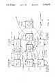
- FIGS. 3A through 3Cjointly depict a detailed logic diagram of a portion of the A delay path 25A, namely, the A delay line 26A, the shared delay line 30 (which is shared with the B delay path 25B) and the binary counter 27A.
- the A delay line 26A and the shared delay line 30include a set of delay elements, generally identified by reference numeral 40(i)(j).
- the index "i" in reference numeral 40(i)(j)which can comprise an integer from the group “1,” “4,” “16,” and “58,” identifies a relative amount of delay that can be provided by the delay element.
- the delay elements 40(i)(j)are serially interconnected by multiplexers 42A through 42D, under control of the AC(8:1) counter control signals, to provide incrementally larger or smaller amounts of delay.
- the delay elements 40(i)(j)are connected in four serially-connected ranks 41A through 41D, with each rank being associated with one value of the index (i).
- the first delay element 40(58)(1) of the first rank 41Areceives the SYS CLK IN system clock in signal, and the delay elements 40 of the first rank 41A comprise the shared delay line 30.
- the delay elements 40(i)(j) in each rank 41are connected in series, and the index (i) in reference numeral 40(i)(j) identifies the position of the delay element 40(i)(j) in the series comprising the rank 41.
- all of the delay elements 40(i)(j) in a rank 41provide the same amount of delay, and the amount of delay provided by a single delay element 40(i)(j) of a rank 41C and 41B is one delay period greater than that provided by the delay elements of the succeeding ranks 41B and 41A in the series.
- the amount of delay provided by a delay element 40(58)(j) in rank 41Ais slightly less than the amount of delay provided by the delay elements of succeeding ranks 41C through 41A.
- the A delay pathalso includes a set of multiplexers 42A through 42D (generally identified by reference numeral 42), each associated with one of the ranks 41A through 41D, for connecting the rank to the succeeding rank.
- Each multiplexer 42is controlled by two of the AC(8:1) counter signals from counter 27A, to establish the incremental amount of delay for the rank.
- Each multiplexer 42includes four signal input terminals that receives input signals from nodes 43A(0) through 43D(3) that are associated with the delay elements 40(i)(j) in its rank. That is, in rank 41A, signals at nodes 43A(0) through 43A(3), which corresponds respectively to:
- the multiplexer 42Aalso includes two control terminals which receive the two high-order binary encoded AC(8:7) counter signals, which enable the multiplexer to couple the signal from one of the nodes 43(A)(0), as identified by the binary-encoded value of the AC(8:7) counter signals, to the next rank.
- multiplexer 42Dprovides a PREL A DEL CLK preliminary delayed clock signal whose edges are delayed from the corresponding edges of the SYS CLK IN system clock input signal by an amount determined by the AC(8:1) counter signals.
- the A delay path 26Aalso includes a fine delay circuit 44 that provides a fine delay adjustment in response to the AC(0) counter signal.
- the fine delay circuit 44includes a delay element 45 and a multiplexer 46 which transmits the A DEL CLK delayed clock signal under control of the AC(0) counter signal.
- the delay element 45receives the PREL A DEL CLK preliminary delayed clock signal, and provides an output signal that has an additional one-half increment of delay. Both the output signal from the delay element 45 and the PREL A DEL CLK preliminary delayed clock signal are coupled to signal input terminals of the multiplexer 46.
- the multiplexer 46couples the PREL A DEL CLK preliminary delayed clock signal to its output terminal as the A DEL CLK delayed clock signal.
- the multiplexer 46couples the output signal from the delay element 45 to its output terminal, to thereby provide and additional one-half increment of delay.
- the A delay path 25Acan provide amounts of delay which vary from zero, if the binary-encoded value of the AC(8:0) counter signals is zero, to two hundred thirty-seven and one-half units of delay, if the binary-encoded value of the AC(8:0) counter signals is five hundred and eleven, in increments of one-half unit.
- each delay element 40(58)(j) in the first rank 41Adoes not provide an amount of delay equal to the delay provided by all of the delay elements 40(i)(j) of the succeeding ranks 41B through 41D. Accordingly, the change in delay as a function of changing the binary value of the AC(8:0) counter signals will not be precisely linear. Instead, there will be slight discontinuities, in particular a reduction of approximately five and one-half increments of delay, when the binary encoded values of the AC(8:7) counter signals change.
- this slight reduction provided in the first rankreduces the likelihood of large differentially non-linear increases or decreases in the amount of delay provided when the multiplexer 42A adds or deletes delays provided by delay elements 40(58)(j) in response to changes in the AC(8:7) counter signals. If delay elements of sufficient accuracy can be provided for the first rank 41A, the aforementioned reduction is not necessary.
- Each of the delay elements 40(58)(j) of the first rank 41Ais shown in FIGS. 3A and 3B as comprising two delay devices 50(28) and two inverters 51(1), with the index identifying the relative amount of delay provided thereby.
- the delay elements 40(16)(j) of the second rank 41Bis shown as comprising two delay devices 52(7) and two inverters 53(1).
- Delay elements providing lengthy delays, such as those used in ranks 41A and 41Bmay tend to provide output signals with somewhat different duty cycles as the input signals.
- dividing the delay elements into multiple delay devices interleaved with invertershelps to ensure that the output signal provided by the delay element will have the same duty cycle as the delay element's input signal.
- the delay elements 40(58)(j) in the first rank 41Acomprise the shared delay line 30, which is shared with the B delay path 25B.
- Delay elements 40(58)(j)can be shared since the selection of the amount of delay provided by the first rank is performed by multiplexer 42A, which follows in the circuit after all of the delay elements 40(58)(j) in the circuit.
- FIG. 3Cdepicts a logic diagram of the counter 27A in the A delay path 25A.
- the counteris a nine-stage binary counter that includes data input terminals D8 through D0, which are used to receive an initial value which can be loaded into the counter, a load enabling terminal LD, a count up terminal UP and a count down terminal DN.
- the counter 27Agenerates, as output signals, nine AC(8:0) counter output signals having binary encoded values ranging between zero and five hundred and eleven.
- the delay control circuit 22initially establishes the value of the counter 27A at the middle of its range, which may be selected as two hundred fifty five or two hundred and fifty six. In the embodiment shown in FIG.
- the initial valueis selected to be two hundred and fifty six, which can be established by connecting the D7 through D0 data input terminals to ground and energizing the D8 data input terminal.
- the D8 data input terminalcan be connected to ground, and the D0 through D7 data input terminals energized, which would provide an initial value of two hundred and fifty five.
- the delay control circuit 22can enable the counter to load the initial value by asserting the A LD load signal.
- the delay control circuitcan enable the counter to alternately count up and down by asserting the A UP count up or A DN count down signal, which energize the count up terminal UP or count down terminal DN, respectively.
- the counter 27Aasserts and negates selected ones of the AC(8:0) counter signals in a conventional manner having increased or decreased binary encoded values to enable the A delay line 26A to increase or decrease the delay provided thereby.
- the counter 27Awhen the counter 27A counts beyond either end of its range it asserts the A WRAP signal which enables the delay control circuit 22 enables the counter to re-load its initial value.
- the counter 27Ahas counted beyond an end of its range when it generates value zero, which can occur if the counter counts down from value one or up from value two hundred and fifty five. In either case, the value zero is represented by the negation of all of the AC(8:0) counter signals.
- the input terminals of a set of inverters 60are connected to receive all of the AC(8:0) counter signals.
- the output terminals of the inverters 60are, in turn, connected to input terminals of an AND gate 61.
- all of the inverters 60When all of the AC(8:0) counter signals are negated, all of the inverters 60 energize all of the input terminals of the AND gate 61, enabling it to assert the A WRAP signal, which is coupled to the delay control circuit 22 over the delay status bus 24.
- the selector circuit 31selects one of the A DEL CLK delayed clock signal, from A delay path 25A, or the B DEL CLK delayed clock signal, from B delay path 25B.
- the selector 31makes the selection in response to the DEL PATH SEL delay path select signal from the delay control circuit 22.
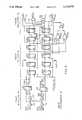
- FIG. 4depicts a logic diagram of selector 31.
- the selector 31includes a multiplexer 70, which receives at its data input terminals the A DEL CLK delayed clock signal and the B DEL CLK delayed clock signal.
- the multiplexer 70couples one of these signals, as selected by a PATH MUX CTRL path multiplexer control signal from a multiplexer control circuit 71, as the COMP DEL CLK composite delayed clock signal.
- a PATH MUX CTRL path multiplexer control signalWhen the PATH MUX CTRL path multiplexer control signal is negated, the multiplexer 70 couples the A DEL CLK delayed clock signal as the COMP DEL CLK composite delayed clock signal, and when the PATH MUX CTRL path multiplexer control signal is asserted, the multiplexer 70 couples the B DEL CLK delayed clock signal as the COMP DEL CLK composite delayed clock signal.
- the multiplexer control circuit 71operates in response to the DEL PATH SEL delay path select signal from the delay control circuit 22 and the SYS CLK IN system clock in signal.
- the multiplexer control circuitincludes two sections, including a buffer section 72 and a synchronizer section 73.
- the buffer section 72buffers the PATH MUX CTRL path multiplexer control signal from the DEL PATH SEL delay path select signal
- the synchronizer section 73ensures that PATH MUX CTRL path multiplexer control signal does not enable the multiplexer 70 to change state unless both the A DEL CLK delayed clock signal and the B DEL CLK delayed clock signal are in a low-voltage state.
- the buffer section 72includes three flip-flops 74, 75 and 76 which operate as a delay line, with the DEL (i) DPS delayed ("i" ticks) delay path select signal ("i" being an integer from 1 to 3) output signal from each successive flip-flop reflecting the condition of the DEL PATH SEL delay path select signal delayed by one, two or three ticks (as identified by the value of "i") of the SYS CLK IN system clock in signal.
- An exclusive-NOR gate 80receives the signals at the data input and output terminals of the flip-flop 76, and controls the condition of a multiplexer 81 which, in turn, determines the source of a signal coupled to the data input terminal of a fourth flip-flop 82 in the buffer section.
- the multiplexer 81determines whether the data input terminal of flip-flop 82 receives the DEL (3) DPS delayed (3 ticks) delay path select signal from flip-flop 76 or a CUR PATH current path signal transmitted by the flip-flop 82.
- the exclusive-NOR gate 80, multiplexer 81 and flip-flop 82reduce the susceptibility of the CUR PATH current path signal to noise that may be present in the DEL PATH SEL delay path select signal from the delay control circuit 22.
- the DEL (2) DPS and DEL (3) DPS delayed ("i" ticks) delay path select signalswill be the same.
- the exclusive-NOR gate 80generates an asserted CH DEL change delay signal, which, in turn, enables multiplexer 81 to couple the DEL (3) DPS delayed (3 ticks) delay path selection signal from the output terminal of flip-flop 76 to the data input terminal of the next flip-flop 82 in the buffer section 72.
- the flip-flop 82transmits a CUR PATH current path signal reflecting the current state of the DEL PATH SEL delay path select signal.
- the new state of the DEL PATH SEL delay path select signalwill be latched first by the flip-flop 74 and next by the flip-flop 75, in response to successive edges of the SYS CLK IN system clock in signal.
- the state of the DEL (2) DPS delayed (2 ticks) delay path select signal input to flip-flop 76is the complement of the DEL (3) DPS delayed (3 ticks) delay path select signal, and will reflect the new state of the DEL PATH SEL delay path select signal.
- the exclusive-NOR gate 80Since the states of the DEL (2) DPS delayed (2 ticks) delay path select signal and the DEL (3) DPS delayed (3 ticks) delay path select signal are complementary, the exclusive-NOR gate 80 generates a negated CH DEL change delay signal. In response, multiplexer 81 is conditioned to couple the CUR PATH current path signal, transmitted by another flip-flop 82 in the buffer section 72, to the data input terminal of the same flip-flop 82, enabling the flip-flop to maintain its state.
- the next edge of the SYS CLK IN system clock in signalwill enable the flip-flop 76 to latch the DEL (2) DPS delayed (2 ticks) delay path select signal.
- the DEL (3) DPS delayed (3 ticks) delay path select signalwill have the same condition as the DEL (2) DPS delayed (2 ticks) delay path select signal.
- the input signals to exclusive-NOR circuit 80will have the same state, resulting in assertion of the CH DELAY change delay signal.
- the asserted CH DELAY change delay signalenables the multiplexer 81 to couple the DEL (3) DPS delayed (3 ticks) delay path select signal to the data input terminal of the flip-flop 82.
- Flip-flop 82will latch the DEL (3) DPS delayed (3 ticks) delay path select signal coupled to it by multiplexer 81 in response to the next edge of the SYS CLK IN system clock in signal. At that point, the CUR PATH current path signal will have the same state as the DEL (3) DPS delayed (3 ticks) delay path select signal.
- the exclusive-NOR gate 80will maintain the CH DELAY change delay signal in an asserted condition, enabling the multiplexer 81 to couple the DEL (3) DPS delayed (3 ticks) delay path select signal to flip-flop 82.
- the combination of the flip-flop 76, exclusive-NOR gate 80 and multiplexer 81reduces the susceptibility of the buffer 72 to noise in the DEL PATH SEL delay path select signal.
- the noisemay be reflected in momentary changes in the condition of the DEL PATH SEL delay path select signal as received at flip-flop 74.
- the DEL PATH SEL delay path select signalis noisy, such that it changes state momentarily and then returns to its original state, those changes will be reflected in the states of the succeeding DEL (i) DPS delayed ("i" ticks) delay path select signals.
- the DEL (2) DPS and DEL (3) DPS delayed ("i" ticks) delay path select signalswill have complementary and alternating conditions at two successive edges of the SYS CLK IN system clock in signal, rather than just one.
- the exclusive-NOR gate 80will continue negating the CH DELAY change delay signal, enabling, in turn, the multiplexer 81 to continue coupling the CUR PATH current path signal to the data input terminal of flip-flop 82 and thereby inhibiting any change in the condition of the flip-flop 82 or the CUR PATH current path signal transmitted thereby.
- the flip-flop 76, exclusive-NOR gate 80 and multiplexer 82provide a degree of immunity from noise in the DEL PATH SEL delay path select signal.
- the synchronizer section 73includes a flip-flop 83 which receives at its data input terminal the CUR PATH current path signal from the buffer section 72 and which transmits the PATH MUX CTRL path multiplexer control signal for controlling the multiplexer 70.
- the flip-flop 83is clocked by an AND gate 84 which has two input terminals, one energized by a NOR gate 85 and the other energized by a state change detection circuit 86.
- the state change detection circuit 86detects when the states of the CUR PATH current path signal and PATH MUX CTRL path multiplexer control signal differ, and at that time energizes its input terminal of the AND gate 84.
- the state change detection circuitincludes an exclusive-OR gate 87 and a flip-flop 90.
- the exclusive-OR gate 87receives the CUR PATH current path and PATH MUX CTRL path multiplexer control signals and is energized only if the two signals differ. This occurs if the multiplexer 70 is switch between the delay paths 25A and 25B. If the exclusive-OR gate 87 is energized, the flip-flop 90 is set in response to the next edge of the SYS CLK IN system clock in signal, thereby transmitting an asserted signal to one input terminal of the AND gate 84.
- the NOR gate 85which controls the other input terminal of AND gate 84, is controlled by the A DEL CLK delayed clock and B DEL CLK delayed clock signals. In particular, the NOR gate 85 generates an asserted output signal only if both of the delayed clock signals are negated.
- the AND gate 84asserts a CLK FF clock flip-flop signal, whose edge clocks the flip-flop 83.
- the flip-flop 83latches the CUR PATH current path signal, which it transmits as the PATH MUX CTRL path multiplexer control signal to control the multiplexer 70.
- the synchronizer section 73thus (1) avoids clocking the flip-flop 83 unless the condition of the CUR PATH current path signal differs from that of the PATH MUX SEL path multiplexer select signal, and then (2) only at points in time at which both the A DEL CLK and B DEL CLK delayed clock signals are in their low voltage conditions.
- the secondminimizes the likelihood of noise which may occur in the COMP DEL CLK composite delay clock signal which can result if the multiplexer 70 is switched while either of the A DEL CLK or B DEL CLK delayed clock signals are in their high voltage conditions.
- the firstensures that the flip-flop 83 is clocked only when necessary, similarly reducing the likelihood of noise.
- the selector 31also operates in response to the global RESET signal from a system controller (not shown) which controls a system including the chip containing the clock buffer circuit 10.
- the RESET signalinitially conditions the flip-flops of the selector 31 to generate a PATH MUX CTRL path multiplexer control signal which, in turn, conditions the multiplexer 70 to couple the B DEL CLK delayed clock signal from the B delay path 25B as the COMP DEL CLK composite delayed clock signal.
- FIG. 5contains a state diagram which is useful in understanding the states maintained by delay state machine 33.
- each blockrepresents a state of the delay state machine 33, and each arrow represents a transition.
- Each arrowis also marked with the logical combination of input signals received by the delay state machine 33 which causes the particular transition. In cases in which arrows extend from block to block, they represent transitions from one state to another. In other cases, in which arrows extend from and return to the same block, the arrows represent transitions from a state to the same state.
- the manner in which input signals is logically combinedis indicated using conventional Boolean logic symbols, that is, a "V" representing a Boolean OR operation, and an upside-down " ⁇ " representing a Boolean AND operation.
- the state of a signal which may give rise to a transitionis indicated by whether the signal name has a bar thereover; if the signal name has no bar over it, the indicated transition may occur if the signal is asserted, but if the signal name does have a bar thereover, a transition may occur if the signal is negated.
- FIG. 5actually represents approximately half of the states maintained by delay state machine 33, in particular those relating to A delay path 25A.
- the states maintained by B delay path 25B, and signals causing transitions therebetween,are similar. Accordingly, a description of states and transitions relating to the A delay path 25A should suffice for an understanding of the operation of the delay state machine 33.
- the delay state machine 33is initially in a state 91 ("B DELAY LINE"), it is asserting the DEL PATH SEL delay path select signal, enabling the selector 31 to couple the B DEL CLK delayed clock signal as the COMP DEL CLK composite delayed clock signal.
- the interval counter 34(FIG. 2) has counted out, so that delay state machine 33 has asserted the DEL PATH SEL delay path select signal for a period of time determined by the interval counter 34.
- the delay state machine 33sequences to a state 92 ("INC A CTR"). In that state, the delay state machine iteratively asserts the A UP count up signal a predetermined number of times, and thereafter determines whether the A DEL CLK delayed clock signal from A delay path 25A lags the B DEL CLK delayed clock signal. The number of times the delay state machine 33 asserts the A UP count up signal is determined by the transition counter 35. Accordingly, in state 92, the delay state machine 33 actually maintains several sub-states, in which it:
- (ii)Iteratively asserts the A UP count up signal.
- the counter 27Auses the A UP count up control signal as described above.
- an OR gate 38receives the A UP count up signal and enables the transition counter 35 to count up. When the transition counter 35 has counted out, it asserts a CTR STATE DEL counter state delay signal.
- the delay state machinestops assertions of the A UP count up signal and instead asserts an LD INT CTR load interval counter signal enabling the interval counter 34 to load an initial value. Thereafter, the interval counter 34 increments in response to ticks of the SYS CLK IN system clock in signal. When the interval counter counts out, it asserts a INT CTR interval counter signal.
- the delay state machine 33In response to the INT CTR interval counter signal from interval counter 34, the delay state machine 33 tests the A LAG B and A WRAP signals. If these signals are negated, the delay state machine 33 performs a transition in which it returns to state 92 and again initiates the above-described operations. If, however, the delay state machine 33 determines, when the interval counter 34 has asserted the INT CTR interval counter signal in sub-state (iii) above, that (a) the A LAG B signal is asserted, indicating that the A DEL CLK delayed clock signal lags the B DEL CLK delayed clock signal, and (b) the A WRAP signal is negated, it sequences to a state 93 ("DEC A CTR").
- the delay state machine 33in one or more iterations, asserts the A DN count down signal to enable the counter 27A to count down, decreasing the delay provided by the A delay path, and following each assertion, enables the interval counter 34 and, after the counter 34 has counted out, tests the A LEAD B signal. If the A LEAD B signal is not asserted at the end of an iteration, the delay state machine performs another iteration.
- the delay state machine 33effectively enables a delay in A delay path 25A which is incrementally less than the delay currently provided by the B delay path 25B. More specifically, in state 93, the delay state machine 33 maintains three sub-states, in which it:
- the delay state machine 33In response to the INT CTR interval counter signal from interval counter 34, the delay state machine 33 tests the conditions of the A LEAD B and A WRAP signals. If these signals are negated, the delay state machine 33 performs a transition in which it returns to state 93 and again initiates the above-described operations. If, however, the delay state machine 33 determines, when the interval counter 34 has asserted the INT CTR interval counter signal in sub-state (ii) above, that (a) the A LEAD B signal is asserted, indicating that the A DEL CLK delayed clock signal leads the B DEL CLK delayed clock signal, and (b) the A WRAP signal is negated, it sequences to a state 94 ("SWITCH TO A DELAY LINE").
- the delay state machine 33negates the DEL PATH SEL delay path select signal, enabling the selector 31 (FIG. 2) to couple the A DEL CLK delayed clock signal as the COMP DEL CLK composite delayed clock signal.
- the delay state machine 33asserts the LD INT CTR load interval counter signal to load an initial value into the interval counter 34.
- the delay state machine 33sequences to a state 95 ("A DELAY LINE"), which corresponds to the state 91.
- the delay state machine 33sequences to state 96 and thereafter state 97, which are analogous to states 92 and 93 described above and will not be described in detail. It will be appreciated that in state 96 the delay state machine 33 in part uses the A LEAD B signal (instead of the A LAG B signal used in state 92) to determine whether to sequence out of the state, and in state 97 it uses in part the A LAG B signal (instead of the A LEAD B signal used in state 93) to determine whether to sequence out of the state. Following step 97, the delay state machine 33 normally will sequence to state 94 and thereafter to state 95, as described above.
- the delay state machine 33enters or remains in any of states 92, 93, 96 or 97 if the A WRAP signal from counter 27A (FIG. 2) is negated. If the A WRAP signal is ever asserted when the delay state machine 33 is in any of these states, it sequences to a state 100. In state 100, the delay state machine first asserts the A LD load enabling signal. As described above, the A LD load enabling signal enables the counter 27A to load an initialization value in the middle of its value range.
- the delay state machine 33enables the determination whether the resulting A DEL CLK delayed clock signal lags the B DEL CLK delayed clock signal, as indicated by the state of the A LAG B signal. If so, the delay state machine sequences to state 92, and otherwise it sequences to state 96.
- State 100thus comprises three sub-states, in which the delay state machine 33:
- Counter 27Auses the signal as described above.
- the delay state machine 33In response to the assertion of the IN CTR interval counter signal from interval counter 34, the delay state machine 33 tests the condition of the A LAG B signal from phase comparator 32A. If the A LAG B signal is asserted, the delay state machine 33 sequences to state 92, and if it is negated the delay state machine sequences to state 96. In either case, the delay state machine 33 thereafter operates as described above.
- FIG. 5depicts states of the delay state machine that relate only to the A delay path 25A. It will be appreciated that the state diagram shown in FIG. 5 can be completed, to include the states relating to the B delay path 25B, by reflecting the diagram around a vertical axis between blocks 91 and 95 and interchanging "A" and "B" in the reflected portion. If the delay state machine 33 is in state 95 following adjustment of the delay provided by A delay path 25A, the delay state machine 33 remains in that state 95 if the PH OK in-phase signal from phase comparator 23 (FIG. 1) is asserted.
- the delay state machine 33sequences instead to a state corresponding to state 92 and performs operations similar to those described above in connection with the delay counter 27B and using signals from the phase counter 32B.
- the LEAD or PH BAD out-of-phase signalis asserted delay state machine sequences to a state corresponding to state 96 and performs operations similar to those described above, also in connection with the delay counter 27B and using signals from the phase counter 32B.
- FIG. 6depicts a logic diagram of a circuit for phase comparator 23 (FIG. 1) useful in the clock buffer circuit 10.
- the phase comparator 23includes three major elements, including a phase detector 110, a phase filter 111 and a phase decoder 112.
- the phase detector 110receives the SYS CLK IN system clock in signal and the DEL CLK OUT REF delayed clock out reference signal from the driver 16 (FIG. 1) and generates in response thereto a COMP LAT REF/SYS-DEL complement latched reference/system-delayed signal and a COMP LAT REF-DEL/SYS complement latched reference-delayed/system signal.
- the phase filter 111receives these signals, delays and filters them, and generates complementary output signals for each of the received signals.
- the phase decoder 112receives the complementary output signals and generates the LAG, LEAD, PH OK in-phase, and PH BAD out-of-phase signals for transmission to the delay control circuit 22.
- the phase detector 110asserts and negates the COMP LAT REF/SYS-DEL complement latched reference/system-delayed signal and a COMP LAT REF-DEL/SYS complement latched reference-delayed/system signal in response to selected phase relationships between the SYS CLK IN system clock in and DEL CLK OUT REF delayed clock out reference signals.
- the phase detector 110includes two buffers 113 and 114 that receive the SYS CLK IN system clock in and DEL CLK OUT REF delayed clock out reference signals, respectively. Each buffer 113 and 114 couples its respective input signal to an input terminal of a flip-flop 115 and 116, respectively, and to an input terminal of a delay element 117 and 120, respectively.
- Delay element 117receives a signal from buffer 113 and in response generates a SYS DEL system delayed signal, which is similar to the SYS CLK IN system clock in signal, but with edges delayed by an amount determined by buffer 113 and delay element 117.
- delay element 120receives a signal from buffer 114 and in response generates a REF DEL reference delayed signal, which is similar to the DEL CLK OUT REF delayed clock out reference signal, but delayed by an amount determined by buffer 113 and delay element 120.
- Buffers 113 and 114may provide similar delay periods, which may thus be ignored in the following discussion of operation of phase detector 110, but delay element 117 provides a longer delay period than delay element 120.
- Flip-flops 115 and 116essentially compare the timings of the edges of the REF DEL reference delayed and DEL CLK OUT REF delayed clock out reference signals to the timing of the edges of the SYS CLK IN system clock in and SYS DEL system delayed signals, respectively.
- the delay defined by delay element 117defines a window in time following a leading edge of the SYS CLK IN system clock in signal such that, if either the DEL CLK OUT REF delayed clock out reference signal or the REF DEL reference delayed signal falls within the window, the phase comparator 23 asserts the PH OK in-phase signal, indicating that the signals are in phase.
- the flip-flop 116receives at its data input terminal the DEL CLK OUT REF delayed clock out reference signal and is clocked by the SYS DEL system delayed signal from delay element 117. If the DEL CLK OUT REF delayed clock out reference signal is asserted at the leading edge of the SYS DEL system delayed signal, which will be the case if the DEL CLK OUT REF delayed clock out reference signal is either in-phase with or leads the SYS CLK IN system clock in signal, the flip-flop 116 is set, thereby negating the COMP LAT REF/SYS-DEL complement latched reference/system-delayed signal.
- the flip-flop 116is cleared, thereby asserting the COMP LAT REF/SYS-DEL complement latched reference/system-delayed signal.
- the flip-flop 115receives at its data input terminal the REF DEL reference delayed signal from the delay element 120 and is clocked by the SYS CLK IN system clock in signal. If the REF DEL reference delayed signal is negated at the leading edge of the SYS CLK IN system clock in signal from buffer 113, which will be the case if the DEL CLK OUT REF delayed clock out reference signal is either in phase with or lags the SYS CLK IN system clock in signal, the flip-flop 115 is cleared, thereby asserting the COMP LAT REF-DEL/SYS complement latched reference-delayed/system signal.
- the flip-flop 115is set, thereby negating the COMP LAT REF-DEL/SYS complement latched reference-delayed/system signal.
- the phase filter 111includes two filter paths 121A and 121B which delay and filter the received COMP LAT REF/SYS-DEL complement latched reference/system-delayed and COMP LAT REF-DEL/SYS complement latched reference-delayed/system signals, respectively, and which generate filtered and complementary signals in response thereto.
- the filter paths 121A and 121Bare generally similar to each other, and so only filter path 121A will be described.
- Filter path 121Aincludes flip-flops 122A through 125A and 127A, a multiplexer 126A, and an exclusive-OR gate 130A.
- phase filter 111includes an AND gate 131, controlled by exclusive-OR gate 130A and the corresponding exclusive-OR gate 130B of filter path 121B, which control both multiplexers 126A and 126B in unison.
- the filter paths 121A and 121Bare structured and operate in a manner similar to buffer section 72 (FIG. 4) of the selector 31, and will not be described further.
- the flip-flop 127A of filter path 121Atransmits, from its Q and Q-bar output terminals, respectively, the true and complement of the COMP LAT REF/SYS-DEL complement latched reference/system-delayed signal, as delayed and filtered by filter path 121A.
- the flip-flop 127B of filter path 121Btransmits, from its Q and Q-bar output terminals respectively, the true and complement of the COMP LAT REF-DEL/SYS complement latched reference-delayed/system signal as delayed and filtered by filter path 121B. All of the signals from the flip-flops 127A and 127B are coupled to the phase decoder 112.
- Phase decoder 112comprises a series of AND gates 132 through 135 that generate the LAG, LEAD, PH OK in-phase, and PH BAD out-of-phase signals, respectively.
- AND gate 132receives the signals from the Q output terminals of both flip-flops 127A and 127B, which, in turn, correspond to the true of both the COMP LAT REF/SYS-DEL complement latched reference/system-delayed signal and the COMP LAT REF-DEL/SYS complement latched reference-delayed/system signal.
- AND gate 133receives the signals from the Q-bar output terminals of both flip-flops 127A and 127B, which, in turn, correspond to the complement of both the COMP LAT REF/SYS-DEL complement latched reference/system-delayed signal and the COMP LAT REF-DEL/SYS complement latched reference-delayed/system signal.
- AND gate 134receives one signal from the Q-bar output terminal of flip-flop 127A, which corresponds to the complement of the COMP LAT REF/SYS-DEL complement latched reference/system-delayed signal, and a second signal from the Q output terminal of flip-flop 127B, which corresponds to the true of the COMP LAT REF-DEL/SYS complement latched reference-delayed/system signal.
- AND gate 135receives a signal from the Q output terminal of flip-flop 127A, which corresponds to the true of the COMP LAT REF/SYS-DEL complement latched reference/system-delayed signal, and a second signal from the Q-bar output terminal of flip-flop 127B, which corresponds to the complement of the COMP LAT REF-DEL/SYS complement latched reference-delayed/system signal.
- phase comparator 23generates the four signals LAG, LEAD, PH OK in-phase and PH BAD out-of-phase signals used by the delay control circuit 22 as described above.
- the clock buffer circuit 10 described above in connection with FIGS. 1 through 6can provide several advantages. As noted above, the circuit 10 can control the timing of edges of the DEL CLK OUT REF delayed clock output reference signal, and thus corresponding edges of the DEL CLK OUT delayed clock output signals, in relation to corresponding edges the SYS CLK IN system clock in signal, obviating problems that may result from timing differences among chips which may result from tolerances and variations in manufacturing processes. This can reduce manufacturing costs that might normally be imposed by tight manufacturing tolerances or that might be required to screen chips after manufacture. Alternatively, the buffer circuit 10 can enable a corresponding increase in processing, since variations in the timings of the DEL CLK OUT delayed clock output signals among the various chips comprising a system can be controlled or reduced.
- variable delay element 20includes phase comparators 32A and 32B that directly measure the phase relationships between the A DEL CLK and B DEL CLK delayed clock signals from the A and B delay paths 25A and 25B.
- phase comparators 32A and 32Bmay be eliminated, with the phase differences being reflected in the difference between the binary-encoded values of the AC(8:0) and BC(8:0) counter signals.
- variable delay element 20may be implemented with a single delay path 25, instead of two delay paths 25A and 25B (FIG.2).
- the variable delay element 20may merely include a single delay line, such as the shared delay line 30 and A delay line 26A (FIGS. 3A and 3B), in which case the phase comparators 32A and 32B and selector 31 would not be necessary.
- the delay clock signal(corresponding to the A DEL CLK signal) may have some noise as a result of changes in the conditions of the multiplexers corresponding to multiplexers 42A through 42D in the delay line.
- the amount of noisemay not be a problem with the controlled circuitry, or the buffer 11 and clock network 15 may have sufficient capacitance that the noise does not reach the controlled circuitry.
- the variable delay elementmay include circuitry for detecting when the A DEL CLK delay clock signal is negated, and change the conditions of the multiplexers controlling the delay line only then, thereby avoiding generation of noise.
- the amount of delay through the buffer 11may be reasonably predictable, it may be possible to add an additional delay element in the clock signal path either at the input terminal at which the variable delay element 20 receives the SYS CLK IN system clock in signal or at the output terminal at which it transmits the COMP DEL CLK composite delay clock signal.
- an invertermay be provided at the input terminal to the variable delay element 20 provide the desired delay.
- the delay provided by the various delay paths 25A and 25B of the variable delay element 20will be several times the period of the SYS CLK IN system clock in signal.
- the additional delay elementmay, if the amount of delay through buffer 11 is otherwise reasonably predictable, permit this constraint to be relaxed, extending the low-frequency range that can be accommodated.
Landscapes
- Engineering & Computer Science (AREA)
- Theoretical Computer Science (AREA)
- Physics & Mathematics (AREA)
- General Engineering & Computer Science (AREA)
- General Physics & Mathematics (AREA)
- Pulse Circuits (AREA)
- Stabilization Of Oscillater, Synchronisation, Frequency Synthesizers (AREA)
- Synchronisation In Digital Transmission Systems (AREA)
- Dram (AREA)
Abstract
Description
Claims (35)
Priority Applications (9)
| Application Number | Priority Date | Filing Date | Title |
|---|---|---|---|
| US07/489,079US5118975A (en) | 1990-03-05 | 1990-03-05 | Digital clock buffer circuit providing controllable delay |
| AU71061/91AAU640448B2 (en) | 1990-03-05 | 1991-02-14 | Digital clock buffer circuit providing controllable delay |
| DE69113083TDE69113083T2 (en) | 1990-03-05 | 1991-02-19 | Digital clock buffer circuit with adjustable delay. |
| EP91102364AEP0445574B1 (en) | 1990-03-05 | 1991-02-19 | Digital clock buffer circuit providing controllable delay |
| AT91102364TATE128254T1 (en) | 1990-03-05 | 1991-02-19 | DIGITAL CLOCK BUFFER CIRCUIT WITH ADJUSTABLE DELAY. |
| IE070691AIE910706A1 (en) | 1990-03-05 | 1991-03-04 | Digital clock buffer circuit providing controllable delay |
| JP3038702AJP2892515B2 (en) | 1990-03-05 | 1991-03-05 | Digital clock buffer circuit |
| CA002037593ACA2037593A1 (en) | 1990-03-05 | 1991-03-05 | Digital clock buffer circuit providing controllable delay |
| US07/820,421US5212484A (en) | 1990-03-05 | 1992-01-14 | Digital to analog converter system employing plural digital to analog converters which is insensitive to resistance variations |
Applications Claiming Priority (1)
| Application Number | Priority Date | Filing Date | Title |
|---|---|---|---|
| US07/489,079US5118975A (en) | 1990-03-05 | 1990-03-05 | Digital clock buffer circuit providing controllable delay |
Related Child Applications (1)
| Application Number | Title | Priority Date | Filing Date |
|---|---|---|---|
| US07/820,421Continuation-In-PartUS5212484A (en) | 1990-03-05 | 1992-01-14 | Digital to analog converter system employing plural digital to analog converters which is insensitive to resistance variations |
Publications (1)
| Publication Number | Publication Date |
|---|---|
| US5118975Atrue US5118975A (en) | 1992-06-02 |
Family
ID=23942318
Family Applications (1)
| Application Number | Title | Priority Date | Filing Date |
|---|---|---|---|
| US07/489,079Expired - LifetimeUS5118975A (en) | 1990-03-05 | 1990-03-05 | Digital clock buffer circuit providing controllable delay |
Country Status (8)
| Country | Link |
|---|---|
| US (1) | US5118975A (en) |
| EP (1) | EP0445574B1 (en) |
| JP (1) | JP2892515B2 (en) |
| AT (1) | ATE128254T1 (en) |
| AU (1) | AU640448B2 (en) |
| CA (1) | CA2037593A1 (en) |
| DE (1) | DE69113083T2 (en) |
| IE (1) | IE910706A1 (en) |
Cited By (86)
| Publication number | Priority date | Publication date | Assignee | Title |
|---|---|---|---|---|
| US5212484A (en)* | 1990-03-05 | 1993-05-18 | Thinking Machines Corporation | Digital to analog converter system employing plural digital to analog converters which is insensitive to resistance variations |
| US5214680A (en)* | 1991-11-01 | 1993-05-25 | Hewlett-Packard Company | CMOS pseudo-NMOS programmable capacitance time vernier and method of calibration |
| US5220206A (en)* | 1990-06-29 | 1993-06-15 | Analog Devices, Inc. | Control apparatus with improved recovery from power reduction, and storage device therefor |
| US5231319A (en)* | 1991-08-22 | 1993-07-27 | Ncr Corporation | Voltage variable delay circuit |
| US5239206A (en)* | 1990-03-06 | 1993-08-24 | Advanced Micro Devices, Inc. | Synchronous circuit with clock skew compensating function and circuits utilizing same |
| US5260608A (en)* | 1990-02-06 | 1993-11-09 | Bull, S.A. | Phase-locked loop and resulting frequency multiplier |
| WO1993024998A1 (en)* | 1992-06-04 | 1993-12-09 | Kaplinsky Cecil H | Clock distribution circuit with active de-skewing |
| US5317202A (en)* | 1992-05-28 | 1994-05-31 | Intel Corporation | Delay line loop for 1X on-chip clock generation with zero skew and 50% duty cycle |
| US5327031A (en)* | 1992-03-24 | 1994-07-05 | Bull S.A. | Variable-delay circuit |
| US5414832A (en)* | 1992-12-17 | 1995-05-09 | International Business Machines Corporation | Tunable synchronous electronic communication apparatus |
| US5426390A (en)* | 1992-06-05 | 1995-06-20 | Kabushiki Kaisha Toshiba | Circuit for generating input transition detection pulse |
| US5448195A (en)* | 1992-07-01 | 1995-09-05 | Mitsubishi Denki Kabushiki Kaisha | Semiconductor integrated delay circuit |
| US5459422A (en)* | 1993-06-02 | 1995-10-17 | Advanced Micro Devices, Inc. | Edge selective delay circuit |
| US5465347A (en)* | 1990-09-05 | 1995-11-07 | International Business Machines Corporation | System for reducing phase difference between clock signals of integrated circuit chips by comparing clock signal from one chip to clock signal from another chip |
| US5467041A (en)* | 1993-06-23 | 1995-11-14 | Nec Corporation | Variable delay buffer circuit |
| US5473768A (en)* | 1993-02-24 | 1995-12-05 | Nec Corporation | Clock generator |
| US5486783A (en)* | 1994-10-31 | 1996-01-23 | At&T Corp. | Method and apparatus for providing clock de-skewing on an integrated circuit board |
| US5550514A (en)* | 1993-04-28 | 1996-08-27 | Telefonaktiebolaget Lm Ericsson | Digital controlled xtal osc |
| US5564022A (en)* | 1994-02-09 | 1996-10-08 | Intel Corporation | Method and apparatus for automatically inserting clock buffers into a logic block to reduce clock skew |
| US5568078A (en)* | 1994-12-30 | 1996-10-22 | Hyundai Electronics Industries Co., Ltd. | Clock delay compensating and duty controlling apparatus of a phase-locked loop |
| US5568072A (en)* | 1993-10-11 | 1996-10-22 | Sgs-Thomson Microelectronics S.A. | Circuit indicating the phase relation between several signals having the same frequency |
| US5572719A (en)* | 1994-11-22 | 1996-11-05 | Advanced Micro Devices | Clock control system for microprocessors including a delay sensing circuit |
| US5592632A (en)* | 1991-11-05 | 1997-01-07 | Monolithic System Technology, Inc. | Defect tolerant integrated circuit subsystem for communication between a module and a bus controller in a wafer-scale integrated circuit system |
| US5610543A (en)* | 1994-03-08 | 1997-03-11 | Motorola Inc. | Delay locked loop for detecting the phase difference of two signals having different frequencies |
| US5633608A (en)* | 1993-09-27 | 1997-05-27 | Sgs-Thomson Microelectronics S.A. | Digital delay line |
| US5655113A (en)* | 1994-07-05 | 1997-08-05 | Monolithic System Technology, Inc. | Resynchronization circuit for a memory system and method of operating same |
| US5737587A (en)* | 1991-11-05 | 1998-04-07 | Monolithic System Technology, Inc. | Resynchronization circuit for circuit module architecture |
| US5744991A (en)* | 1995-10-16 | 1998-04-28 | Altera Corporation | System for distributing clocks using a delay lock loop in a programmable logic circuit |
| US5757218A (en)* | 1996-03-12 | 1998-05-26 | International Business Machines Corporation | Clock signal duty cycle correction circuit and method |
| US5774699A (en)* | 1995-07-04 | 1998-06-30 | Kabushiki Kaisha Toshiba | System controller for controlling switching operations of various operation clocks for CPU, DRAM, and the like |
| US5828250A (en)* | 1994-09-06 | 1998-10-27 | Intel Corporation | Differential delay line clock generator with feedback phase control |
| US5831467A (en)* | 1991-11-05 | 1998-11-03 | Monolithic System Technology, Inc. | Termination circuit with power-down mode for use in circuit module architecture |
| US5838179A (en)* | 1996-07-03 | 1998-11-17 | General Signal Corporation | Clock compensation circuit |
| US5843799A (en)* | 1991-11-05 | 1998-12-01 | Monolithic System Technology, Inc. | Circuit module redundancy architecture process |
| US5910740A (en)* | 1997-06-18 | 1999-06-08 | Raytheon Company | Phase locked loop having memory |
| US5999027A (en)* | 1995-06-13 | 1999-12-07 | Fujitsu Limited | Phase compensating apparatus and delay controlling circuit |
| US6055287A (en)* | 1998-05-26 | 2000-04-25 | Mcewan; Thomas E. | Phase-comparator-less delay locked loop |
| US6137334A (en)* | 1998-07-06 | 2000-10-24 | Micron Technology, Inc. | Logic circuit delay stage and delay line utilizing same |
| US6144713A (en)* | 1997-04-10 | 2000-11-07 | Fujitsu Limited | Delay locked loop circuit for controlling delay time with reduced lock-up time |
| US6194930B1 (en)* | 1998-06-11 | 2001-02-27 | Fujitsu Limited | DLL circuit |
| US6229368B1 (en)* | 1998-12-18 | 2001-05-08 | Samsung Electronics Co. Ltd. | Internal clock generating circuits having delay compensation and methods for using the same |
| US6246635B1 (en)* | 1997-10-24 | 2001-06-12 | Takashi Suzuki | Electric and electronic equipment |
| US6246704B1 (en)* | 1998-04-30 | 2001-06-12 | Stmicroelectronics, Inc. | Automatic on-chip clock tuning methodology and circuitry |
| US6320445B1 (en)* | 1998-12-18 | 2001-11-20 | Stmicroelectronics Limited | Circuitry and a method for introducing a delay |
| US6320437B1 (en) | 1998-10-30 | 2001-11-20 | Mosaid Technologies, Inc. | Duty cycle regulator |
| US6384655B1 (en)* | 1999-05-24 | 2002-05-07 | Micron Technology, Inc. | Comparator for determining process variations |
| US6393576B1 (en)* | 1994-11-09 | 2002-05-21 | Adaptec, Inc. | Apparatus and method for communication between integrated circuit connected to each other by a single line |
| US20020080825A1 (en)* | 2000-12-23 | 2002-06-27 | Alcatel | Method and compensation module for the phase compensation of clock signals |
| US6424184B1 (en)* | 1996-09-25 | 2002-07-23 | Matsushita Electric Industrial Co., Ltd. | Frequency-voltage conversion circuit, delay amount judgement circuit, system having frequency-voltage conversion circuit, method of adjusting input/output characteristics of frequency-voltage conversion circuit, and apparatus for automatically adjusting input |
| US6486716B1 (en)* | 1999-09-08 | 2002-11-26 | Nec Corporation | Phase compensation circuit |
| US6501307B1 (en) | 2001-11-12 | 2002-12-31 | Pericom Semiconductor Corp. | Spread-spectrum clock buffer/driver that modulates clock period by switching loads |
| US6501311B2 (en)* | 2000-01-24 | 2002-12-31 | Broadcom Corporation | System and method for compensating for supply voltage induced signal delay mismatches |
| US6621882B2 (en) | 2001-03-02 | 2003-09-16 | General Dynamics Information Systems, Inc. | Method and apparatus for adjusting the clock delay in systems with multiple integrated circuits |
| US6646484B2 (en)* | 2001-12-21 | 2003-11-11 | Mitsubishi Denki Kabushiki Kaisha | PLL circuit including a control logic circuit for adjusting the delay times of the clocks so that the phase error of the clocks is reduced |
| US6651179B1 (en) | 1999-05-10 | 2003-11-18 | Advantest Corporation | Delay time judging apparatus |
| US20040030946A1 (en)* | 2002-08-08 | 2004-02-12 | Carley Adam L. | Clock distributor circuit for maintaining a phase relationship between remote operating nodes and a reference clock on a chip |
| US6720810B1 (en)* | 2002-06-14 | 2004-04-13 | Xilinx, Inc. | Dual-edge-correcting clock synchronization circuit |
| US6727734B2 (en) | 2001-08-29 | 2004-04-27 | Micron Technology, Inc. | Variable delay circuit and method, and delay locked loop, memory device and computer system using same |
| US6748549B1 (en)* | 2000-06-26 | 2004-06-08 | Intel Corporation | Clocking an I/O buffer, having a selectable phase difference from the system clock, to and from a remote I/O buffer clocked in phase with the system clock |
| US20040193769A1 (en)* | 2003-03-25 | 2004-09-30 | Fujitsu Limited | State indicating information setting circuit and status bit setting circuit |
| US20040213051A1 (en)* | 2003-04-28 | 2004-10-28 | Feng Lin | Method and apparatus for improving stability and lock time for synchronous circuits |
| US6831490B1 (en)* | 2000-07-18 | 2004-12-14 | Hewlett-Packard Development Company, L.P. | Clock synchronization circuit and method |
| US6831493B2 (en) | 1998-10-30 | 2004-12-14 | Mosaid Technologies Incorporated | Duty cycle regulator |
| US20050007154A1 (en)* | 2003-07-07 | 2005-01-13 | Patella Benjamin J. | System and method for evaluating the speed of a circuit |
| US20050046458A1 (en)* | 2003-08-28 | 2005-03-03 | Schroeder Charles G. | Digital delay elements constructed in a programmable logic device |
| US20050069019A1 (en)* | 2003-08-26 | 2005-03-31 | Masao Kaizuka | Spread spectrum clock generator |
| US20050262373A1 (en)* | 2004-05-18 | 2005-11-24 | Kim Kang Y | DLL phase detection using advanced phase equal |
| US20060017478A1 (en)* | 2004-07-20 | 2006-01-26 | Micron Technology, Inc. | Delay-locked loop with feedback compensation |
| US20060044931A1 (en)* | 2004-08-31 | 2006-03-02 | Kang Yong Kim | Delay-locked loop having a pre-shift phase detector |
| US20060097763A1 (en)* | 2004-11-10 | 2006-05-11 | Lsi Logic Corporation | Delay locked loop having internal test path |
| US20060146971A1 (en)* | 2003-08-26 | 2006-07-06 | Masao Kaizuka | Spread spectrum clock generator |
| US20060247880A1 (en)* | 2005-04-29 | 2006-11-02 | International Business Machines Corporation | Testable digital delay line |
| US20070139085A1 (en)* | 2005-10-10 | 2007-06-21 | Stmicroelectronics (Research & Development) Limited | Fast buffer pointer across clock domains |
| US20070159213A1 (en)* | 2006-01-11 | 2007-07-12 | Jenkins Keith A | Method and apparatus for measuring and compensating for static phase error in phase locked loops |
| US20080246461A1 (en)* | 2006-05-19 | 2008-10-09 | Abuhamdeh Zahi S | Methods and Apparatus for Testing Delay Locked Loops and Clock Skew |
| US7457822B1 (en) | 2002-11-01 | 2008-11-25 | Bluearc Uk Limited | Apparatus and method for hardware-based file system |
| US20090190631A1 (en)* | 2008-01-29 | 2009-07-30 | Meng-Han Hsieh | Method for generating a spread spectrum clock and apparatus thereof |
| US20090302951A1 (en)* | 2008-06-10 | 2009-12-10 | Qualcomm Incorporated | Dithering a digitally-controlled oscillator output in a phase-locked loop |
| US20090316514A1 (en)* | 1994-10-06 | 2009-12-24 | Foss Richard C | Delay Locked Loop Implementation in a Synchronous Dynamic Random Access Memory |
| US7639054B1 (en)* | 2008-01-16 | 2009-12-29 | Altera Corporation | Techniques for generating programmable delays |
| US8041735B1 (en) | 2002-11-01 | 2011-10-18 | Bluearc Uk Limited | Distributed file system and method |
| US8180897B2 (en) | 1999-10-14 | 2012-05-15 | Bluearc Uk Limited | Apparatus and method for hardware implementation or acceleration of operating system functions |
| TWI623198B (en)* | 2016-10-20 | 2018-05-01 | 國立高雄第一科技大學 | Resolution-enhancing cmos full-digital-structurally pulse mixing method and device thereof |
| US10340931B1 (en)* | 2017-12-30 | 2019-07-02 | Tektronix, Inc. | Dynamic delay adjustment for multi-channel digital-to-analog converter synchronization |
| CN112185440A (en)* | 2019-07-05 | 2021-01-05 | 爱思开海力士有限公司 | Memory interface, data storage device and operation method thereof |
| CN115602215A (en)* | 2021-07-09 | 2023-01-13 | 长鑫存储技术有限公司(Cn) | Enable control circuit and semiconductor memory |
Families Citing this family (12)
| Publication number | Priority date | Publication date | Assignee | Title |
|---|---|---|---|---|
| US5294842A (en)* | 1991-09-23 | 1994-03-15 | Digital Equipment Corp. | Update synchronizer |
| WO1993006497A1 (en)* | 1991-09-23 | 1993-04-01 | Digital Equipment Corporation | Method and apparatus for complete functional testing of a complex signal path of a semiconductor chip |
| JPH07273618A (en)* | 1994-03-30 | 1995-10-20 | Nec Corp | Clock driver circuit |
| JP2771464B2 (en)* | 1994-09-29 | 1998-07-02 | 日本電気アイシーマイコンシステム株式会社 | Digital PLL circuit |
| TW340262B (en) | 1996-08-13 | 1998-09-11 | Fujitsu Ltd | Semiconductor device, system consisting of semiconductor devices and digital delay circuit |
| GB2355097B (en)* | 1996-08-13 | 2001-05-23 | Fujitsu Ltd | Semiconductor device |
| KR100237567B1 (en)* | 1997-05-07 | 2000-01-15 | 김영환 | Delay lock circuit |
| DE69737748T2 (en)* | 1997-05-16 | 2008-01-31 | Fujitsu Ltd., Kawasaki | Skew reducing circuit |
| US5949262A (en)* | 1998-01-07 | 1999-09-07 | International Business Machines Corporation | Method and apparatus for coupled phase locked loops |
| US6522188B1 (en)* | 1998-04-10 | 2003-02-18 | Top Layer Networks, Inc. | High-speed data bus for network switching |
| JP2000035831A (en)* | 1998-07-21 | 2000-02-02 | Nec Corp | Low skew clock tree circuit using variable threshold voltage transistor |
| GB2348327B (en) | 1999-02-18 | 2003-02-19 | Sgs Thomson Microelectronics | Clock skew removal appartus |
Citations (34)
| Publication number | Priority date | Publication date | Assignee | Title |
|---|---|---|---|---|
| US4339823A (en)* | 1980-08-15 | 1982-07-13 | Motorola, Inc. | Phase corrected clock signal recovery circuit |
| US4355387A (en)* | 1979-02-21 | 1982-10-19 | Portejoie Jean Francois | Resynchronizing circuit for time division multiplex system |
| US4365210A (en)* | 1980-06-26 | 1982-12-21 | Motorola, Inc. | Data and clock recovery system having a phase-locked-loop and which controls dynamic loop response of a data stream of unknown data format |
| US4369515A (en)* | 1980-10-06 | 1983-01-18 | Gte Automatic Electric Labs Inc. | Clock synchronization circuit |
| US4390801A (en)* | 1981-06-08 | 1983-06-28 | Trio Kabushiki Kaisha | Circuit for reproducing a clock signal |
| US4412342A (en)* | 1981-12-18 | 1983-10-25 | Gte Automatic Electric Labs Inc. | Clock synchronization system |
| US4475085A (en)* | 1980-09-25 | 1984-10-02 | Tokyo Shibaura Denki Kabushiki Kaisha | Clock synchronization signal generating circuit |
| US4479216A (en)* | 1982-12-22 | 1984-10-23 | At&T Bell Laboratories | Skew-free clock circuit for integrated circuit chip |
| US4504749A (en)* | 1981-07-20 | 1985-03-12 | Takeda Riken Co., Ltd. | Delay pulse generating circuit |
| US4516035A (en)* | 1983-08-22 | 1985-05-07 | Ncr Corporation | Phase synchronization and control circuit |
| US4519086A (en)* | 1982-06-16 | 1985-05-21 | Western Digital Corporation | MOS Phase lock loop synchronization circuit |
| US4573173A (en)* | 1983-06-06 | 1986-02-25 | Nitsuko Limited | Clock synchronization device in data transmission system |
| US4580278A (en)* | 1982-10-26 | 1986-04-01 | Sansui Electric Co., Ltd. | Read clock producing system |
| US4590602A (en)* | 1983-08-18 | 1986-05-20 | General Signal | Wide range clock recovery circuit |
| US4617679A (en)* | 1983-09-20 | 1986-10-14 | Nec Electronics U.S.A., Inc. | Digital phase lock loop circuit |
| US4626798A (en)* | 1985-12-11 | 1986-12-02 | Gte Laboratories Incorporated | Phase-lock loop including integrated circuit voltage controlled oscillator |
| US4633488A (en)* | 1984-11-13 | 1986-12-30 | Digital Equipment Corporation | Phase-locked loop for MFM data recording |
| US4635000A (en)* | 1985-11-12 | 1987-01-06 | Xerox Corporation | Temporal pixel clock synchronization system |
| US4637018A (en)* | 1984-08-29 | 1987-01-13 | Burroughs Corporation | Automatic signal delay adjustment method |
| US4651026A (en)* | 1983-07-06 | 1987-03-17 | Motorola, Inc. | Clock recovery circuit |
| US4663523A (en)* | 1985-11-12 | 1987-05-05 | Xerox Corporation | Spatial pixel clock synchronization system |
| US4680779A (en)* | 1985-01-14 | 1987-07-14 | David Systems, Inc. | Distributed clock synchronization in a digital data switching system |
| US4689575A (en)* | 1985-07-15 | 1987-08-25 | Rca Corporation | Clock synchronization circuit for a computer timer |
| US4692932A (en)* | 1985-02-07 | 1987-09-08 | Alcatel | Triplicated clock distribution device for use when each clock signal comprises a synchonization signal |
| US4700347A (en)* | 1985-02-13 | 1987-10-13 | Bolt Beranek And Newman Inc. | Digital phase adjustment |
| US4744096A (en)* | 1986-01-20 | 1988-05-10 | Alcatel Thomson Faisceaux Hertziens | Clock recovery circuit |
| US4759041A (en)* | 1987-02-19 | 1988-07-19 | Unisys Corporation | Local area network control system synchronization with phase-lock loop |
| US4771196A (en)* | 1987-08-05 | 1988-09-13 | California Institute Of Technology | Electronically variable active analog delay line |
| US4779008A (en)* | 1982-10-11 | 1988-10-18 | U.S. Philips Corporation | Multiple redundant clock system comprising a number of mutually synchronizing clocks, and clock circuit for use in such a clock system |
| US4804928A (en)* | 1987-05-12 | 1989-02-14 | Texas Instruments Incorporated | Phase-frequency compare circuit for phase lock loop |
| US4807266A (en)* | 1987-09-28 | 1989-02-21 | Compaq Computer Corporation | Circuit and method for performing equal duty cycle odd value clock division and clock synchronization |
| US4829377A (en)* | 1988-03-03 | 1989-05-09 | Communications Satellite Corporation | Horizontal synchronization, clock synchronization, D. C. restoration and gain control scheme for an analog TV system |
| US4873491A (en)* | 1987-10-19 | 1989-10-10 | Wilkins Jeffrey K | Phase shift circuit utilizing a variable time delay line |
| US4908841A (en)* | 1987-10-30 | 1990-03-13 | Digital Equipment Corporation | Data decoding circuit including phase-locked loop timing |
Family Cites Families (3)
| Publication number | Priority date | Publication date | Assignee | Title |
|---|---|---|---|---|
| WO1989000311A1 (en)* | 1987-06-30 | 1989-01-12 | Unisys Corporation | Automatic clock de-skewing on a circuit board |
| JP2901657B2 (en)* | 1988-09-14 | 1999-06-07 | 株式会社日立製作所 | Clock signal supply device |
| US5043596A (en)* | 1988-09-14 | 1991-08-27 | Hitachi, Ltd. | Clock signal supplying device having a phase compensation circuit |
- 1990
- 1990-03-05USUS07/489,079patent/US5118975A/ennot_activeExpired - Lifetime
- 1991
- 1991-02-14AUAU71061/91Apatent/AU640448B2/ennot_activeCeased
- 1991-02-19DEDE69113083Tpatent/DE69113083T2/ennot_activeExpired - Fee Related
- 1991-02-19EPEP91102364Apatent/EP0445574B1/ennot_activeExpired - Lifetime
- 1991-02-19ATAT91102364Tpatent/ATE128254T1/ennot_activeIP Right Cessation
- 1991-03-04IEIE070691Apatent/IE910706A1/enunknown
- 1991-03-05CACA002037593Apatent/CA2037593A1/ennot_activeAbandoned
- 1991-03-05JPJP3038702Apatent/JP2892515B2/ennot_activeExpired - Fee Related
Patent Citations (34)
| Publication number | Priority date | Publication date | Assignee | Title |
|---|---|---|---|---|
| US4355387A (en)* | 1979-02-21 | 1982-10-19 | Portejoie Jean Francois | Resynchronizing circuit for time division multiplex system |
| US4365210A (en)* | 1980-06-26 | 1982-12-21 | Motorola, Inc. | Data and clock recovery system having a phase-locked-loop and which controls dynamic loop response of a data stream of unknown data format |
| US4339823A (en)* | 1980-08-15 | 1982-07-13 | Motorola, Inc. | Phase corrected clock signal recovery circuit |
| US4475085A (en)* | 1980-09-25 | 1984-10-02 | Tokyo Shibaura Denki Kabushiki Kaisha | Clock synchronization signal generating circuit |
| US4369515A (en)* | 1980-10-06 | 1983-01-18 | Gte Automatic Electric Labs Inc. | Clock synchronization circuit |
| US4390801A (en)* | 1981-06-08 | 1983-06-28 | Trio Kabushiki Kaisha | Circuit for reproducing a clock signal |
| US4504749A (en)* | 1981-07-20 | 1985-03-12 | Takeda Riken Co., Ltd. | Delay pulse generating circuit |
| US4412342A (en)* | 1981-12-18 | 1983-10-25 | Gte Automatic Electric Labs Inc. | Clock synchronization system |
| US4519086A (en)* | 1982-06-16 | 1985-05-21 | Western Digital Corporation | MOS Phase lock loop synchronization circuit |
| US4779008A (en)* | 1982-10-11 | 1988-10-18 | U.S. Philips Corporation | Multiple redundant clock system comprising a number of mutually synchronizing clocks, and clock circuit for use in such a clock system |
| US4580278A (en)* | 1982-10-26 | 1986-04-01 | Sansui Electric Co., Ltd. | Read clock producing system |
| US4479216A (en)* | 1982-12-22 | 1984-10-23 | At&T Bell Laboratories | Skew-free clock circuit for integrated circuit chip |
| US4573173A (en)* | 1983-06-06 | 1986-02-25 | Nitsuko Limited | Clock synchronization device in data transmission system |
| US4651026A (en)* | 1983-07-06 | 1987-03-17 | Motorola, Inc. | Clock recovery circuit |
| US4590602A (en)* | 1983-08-18 | 1986-05-20 | General Signal | Wide range clock recovery circuit |
| US4516035A (en)* | 1983-08-22 | 1985-05-07 | Ncr Corporation | Phase synchronization and control circuit |
| US4617679A (en)* | 1983-09-20 | 1986-10-14 | Nec Electronics U.S.A., Inc. | Digital phase lock loop circuit |
| US4637018A (en)* | 1984-08-29 | 1987-01-13 | Burroughs Corporation | Automatic signal delay adjustment method |
| US4633488A (en)* | 1984-11-13 | 1986-12-30 | Digital Equipment Corporation | Phase-locked loop for MFM data recording |
| US4680779A (en)* | 1985-01-14 | 1987-07-14 | David Systems, Inc. | Distributed clock synchronization in a digital data switching system |
| US4692932A (en)* | 1985-02-07 | 1987-09-08 | Alcatel | Triplicated clock distribution device for use when each clock signal comprises a synchonization signal |
| US4700347A (en)* | 1985-02-13 | 1987-10-13 | Bolt Beranek And Newman Inc. | Digital phase adjustment |
| US4689575A (en)* | 1985-07-15 | 1987-08-25 | Rca Corporation | Clock synchronization circuit for a computer timer |
| US4635000A (en)* | 1985-11-12 | 1987-01-06 | Xerox Corporation | Temporal pixel clock synchronization system |
| US4663523A (en)* | 1985-11-12 | 1987-05-05 | Xerox Corporation | Spatial pixel clock synchronization system |
| US4626798A (en)* | 1985-12-11 | 1986-12-02 | Gte Laboratories Incorporated | Phase-lock loop including integrated circuit voltage controlled oscillator |
| US4744096A (en)* | 1986-01-20 | 1988-05-10 | Alcatel Thomson Faisceaux Hertziens | Clock recovery circuit |
| US4759041A (en)* | 1987-02-19 | 1988-07-19 | Unisys Corporation | Local area network control system synchronization with phase-lock loop |
| US4804928A (en)* | 1987-05-12 | 1989-02-14 | Texas Instruments Incorporated | Phase-frequency compare circuit for phase lock loop |
| US4771196A (en)* | 1987-08-05 | 1988-09-13 | California Institute Of Technology | Electronically variable active analog delay line |
| US4807266A (en)* | 1987-09-28 | 1989-02-21 | Compaq Computer Corporation | Circuit and method for performing equal duty cycle odd value clock division and clock synchronization |
| US4873491A (en)* | 1987-10-19 | 1989-10-10 | Wilkins Jeffrey K | Phase shift circuit utilizing a variable time delay line |
| US4908841A (en)* | 1987-10-30 | 1990-03-13 | Digital Equipment Corporation | Data decoding circuit including phase-locked loop timing |
| US4829377A (en)* | 1988-03-03 | 1989-05-09 | Communications Satellite Corporation | Horizontal synchronization, clock synchronization, D. C. restoration and gain control scheme for an analog TV system |
Non-Patent Citations (12)
| Title |
|---|
| Horowitz et al., "The Art of Electronics", 2d Ed., (Cambridge Univ. Press, 1989, pp. 512-515, 533 and 1121. |
| Horowitz et al., The Art of Electronics , 2d Ed., (Cambridge Univ. Press, 1989, pp. 512 515, 533 and 1121.* |
| M. G. Gallup et al., Testability Features of 68040, Proceedings of the 1990 International Test Conference, Sep. 10 14, 1990 (IEEE Computer Society Press, 1990), pp. 749 757.* |
| M. G. Gallup et al., Testability Features of 68040, Proceedings of the 1990 International Test Conference, Sep. 10-14, 1990 (IEEE Computer Society Press, 1990), pp. 749-757. |
| M. Johnson et al., "A Variable Delay Line PLL for CPU-Coprocessor Synchronization," IEEE J. Solid-State Circuits, vol. 23, No. 5 (Oct. 1988) pp. 1218-1223. |
| M. Johnson et al., A Variable Delay Line PLL for CPU Coprocessor Synchronization, IEEE J. Solid State Circuits, vol. 23, No. 5 (Oct. 1988) pp. 1218 1223.* |
| P. Bassett et al., "Dynamic Delay Adjustment: A Technique for High-Speed Asynchronous Communication," in ADVANCED RESEARCH IN VLSI, Proc. Fourth MIT Conf. Apr. 7-9, 1986 (C. Leiserson, ed., MIT Press: 1986) pp. 219-232. |
| P. Bassett et al., Dynamic Delay Adjustment: A Technique for High Speed Asynchronous Communication, in ADVANCED RESEARCH IN VLSI, Proc. Fourth MIT Conf. Apr. 7 9, 1986 (C. Leiserson, ed., MIT Press: 1986) pp. 219 232.* |
| R. D. Rettberg et al., The Monarch Parallel Processor Hardware Design, IEEE Computer, Apr., 1990 pp. 18 30.* |
| R. D. Rettberg et al., The Monarch Parallel Processor Hardware Design, IEEE Computer, Apr., 1990 pp. 18-30. |
| R. Rettberg et al., IEEE Computer, vol. 23, No. 4, (Apr. 1990) pp. 18 30.* |
| R. Rettberg et al., IEEE Computer, vol. 23, No. 4, (Apr. 1990) pp. 18-30. |
Cited By (149)
| Publication number | Priority date | Publication date | Assignee | Title |
|---|---|---|---|---|
| US5260608A (en)* | 1990-02-06 | 1993-11-09 | Bull, S.A. | Phase-locked loop and resulting frequency multiplier |
| US5212484A (en)* | 1990-03-05 | 1993-05-18 | Thinking Machines Corporation | Digital to analog converter system employing plural digital to analog converters which is insensitive to resistance variations |
| US5239206A (en)* | 1990-03-06 | 1993-08-24 | Advanced Micro Devices, Inc. | Synchronous circuit with clock skew compensating function and circuits utilizing same |
| US5220206A (en)* | 1990-06-29 | 1993-06-15 | Analog Devices, Inc. | Control apparatus with improved recovery from power reduction, and storage device therefor |
| US5465347A (en)* | 1990-09-05 | 1995-11-07 | International Business Machines Corporation | System for reducing phase difference between clock signals of integrated circuit chips by comparing clock signal from one chip to clock signal from another chip |
| US5231319A (en)* | 1991-08-22 | 1993-07-27 | Ncr Corporation | Voltage variable delay circuit |
| US5214680A (en)* | 1991-11-01 | 1993-05-25 | Hewlett-Packard Company | CMOS pseudo-NMOS programmable capacitance time vernier and method of calibration |
| US5843799A (en)* | 1991-11-05 | 1998-12-01 | Monolithic System Technology, Inc. | Circuit module redundancy architecture process |
| US20040260983A1 (en)* | 1991-11-05 | 2004-12-23 | Monolithic System Technology, Inc. | Latched sense amplifiers as high speed memory in a memory system |
| US5666480A (en)* | 1991-11-05 | 1997-09-09 | Monolithic System Technology, Inc. | Fault-tolerant hierarchical bus system and method of operating same |
| US20080209303A1 (en)* | 1991-11-05 | 2008-08-28 | Mosys, Inc. | Error Detection/Correction Method |
| US5613077A (en)* | 1991-11-05 | 1997-03-18 | Monolithic System Technology, Inc. | Method and circuit for communication between a module and a bus controller in a wafer-scale integrated circuit system |
| US5737587A (en)* | 1991-11-05 | 1998-04-07 | Monolithic System Technology, Inc. | Resynchronization circuit for circuit module architecture |
| US6717864B2 (en) | 1991-11-05 | 2004-04-06 | Monlithic System Technology, Inc. | Latched sense amplifiers as high speed memory in a memory system |
| US5831467A (en)* | 1991-11-05 | 1998-11-03 | Monolithic System Technology, Inc. | Termination circuit with power-down mode for use in circuit module architecture |
| US5592632A (en)* | 1991-11-05 | 1997-01-07 | Monolithic System Technology, Inc. | Defect tolerant integrated circuit subsystem for communication between a module and a bus controller in a wafer-scale integrated circuit system |
| US7634707B2 (en) | 1991-11-05 | 2009-12-15 | Mosys, Inc. | Error detection/correction method |
| US5327031A (en)* | 1992-03-24 | 1994-07-05 | Bull S.A. | Variable-delay circuit |
| US5317202A (en)* | 1992-05-28 | 1994-05-31 | Intel Corporation | Delay line loop for 1X on-chip clock generation with zero skew and 50% duty cycle |
| US5410263A (en)* | 1992-05-28 | 1995-04-25 | Intel Corporation | Delay line loop for on-chip clock synthesis with zero skew and 50% duty cycle |
| WO1993024998A1 (en)* | 1992-06-04 | 1993-12-09 | Kaplinsky Cecil H | Clock distribution circuit with active de-skewing |
| US5298866A (en)* | 1992-06-04 | 1994-03-29 | Kaplinsky Cecil H | Clock distribution circuit with active de-skewing |
| US5426390A (en)* | 1992-06-05 | 1995-06-20 | Kabushiki Kaisha Toshiba | Circuit for generating input transition detection pulse |
| US5448195A (en)* | 1992-07-01 | 1995-09-05 | Mitsubishi Denki Kabushiki Kaisha | Semiconductor integrated delay circuit |
| US5414832A (en)* | 1992-12-17 | 1995-05-09 | International Business Machines Corporation | Tunable synchronous electronic communication apparatus |
| US5473768A (en)* | 1993-02-24 | 1995-12-05 | Nec Corporation | Clock generator |
| US5550514A (en)* | 1993-04-28 | 1996-08-27 | Telefonaktiebolaget Lm Ericsson | Digital controlled xtal osc |
| US5459422A (en)* | 1993-06-02 | 1995-10-17 | Advanced Micro Devices, Inc. | Edge selective delay circuit |
| US5467041A (en)* | 1993-06-23 | 1995-11-14 | Nec Corporation | Variable delay buffer circuit |
| US5633608A (en)* | 1993-09-27 | 1997-05-27 | Sgs-Thomson Microelectronics S.A. | Digital delay line |
| US5719515A (en)* | 1993-09-27 | 1998-02-17 | Sgs-Thomson Microelectronics S.A. | Digital delay line |
| US5568072A (en)* | 1993-10-11 | 1996-10-22 | Sgs-Thomson Microelectronics S.A. | Circuit indicating the phase relation between several signals having the same frequency |
| US5564022A (en)* | 1994-02-09 | 1996-10-08 | Intel Corporation | Method and apparatus for automatically inserting clock buffers into a logic block to reduce clock skew |
| US5610543A (en)* | 1994-03-08 | 1997-03-11 | Motorola Inc. | Delay locked loop for detecting the phase difference of two signals having different frequencies |
| US5729152A (en)* | 1994-07-05 | 1998-03-17 | Monolithic System Technology, Inc. | Termination circuits for reduced swing signal lines and methods for operating same |
| US6754746B1 (en) | 1994-07-05 | 2004-06-22 | Monolithic System Technology, Inc. | Memory array with read/write methods |
| US5655113A (en)* | 1994-07-05 | 1997-08-05 | Monolithic System Technology, Inc. | Resynchronization circuit for a memory system and method of operating same |
| US6272577B1 (en) | 1994-07-05 | 2001-08-07 | Monolithic System Technology, Inc. | Data processing system with master and slave devices and asymmetric signal swing bus |
| US6393504B1 (en) | 1994-07-05 | 2002-05-21 | Monolithic System Technology, Inc. | Dynamic address mapping and redundancy in a modular memory device |
| US5828250A (en)* | 1994-09-06 | 1998-10-27 | Intel Corporation | Differential delay line clock generator with feedback phase control |
| US20090316514A1 (en)* | 1994-10-06 | 2009-12-24 | Foss Richard C | Delay Locked Loop Implementation in a Synchronous Dynamic Random Access Memory |
| US8369182B2 (en) | 1994-10-06 | 2013-02-05 | Mosaid Technologies Incorporated | Delay locked loop implementation in a synchronous dynamic random access memory |
| US8638638B2 (en) | 1994-10-06 | 2014-01-28 | Mosaid Technologies Incorporated | Delay locked loop implementation in a synchronous dynamic random access memory |
| US5486783A (en)* | 1994-10-31 | 1996-01-23 | At&T Corp. | Method and apparatus for providing clock de-skewing on an integrated circuit board |
| US6516366B1 (en) | 1994-11-09 | 2003-02-04 | Adaptec, Incorporated | Serial bus for connecting two integrated circuits with storage for input/output signals |
| US6393576B1 (en)* | 1994-11-09 | 2002-05-21 | Adaptec, Inc. | Apparatus and method for communication between integrated circuit connected to each other by a single line |
| US5572719A (en)* | 1994-11-22 | 1996-11-05 | Advanced Micro Devices | Clock control system for microprocessors including a delay sensing circuit |
| US5568078A (en)* | 1994-12-30 | 1996-10-22 | Hyundai Electronics Industries Co., Ltd. | Clock delay compensating and duty controlling apparatus of a phase-locked loop |
| US5999027A (en)* | 1995-06-13 | 1999-12-07 | Fujitsu Limited | Phase compensating apparatus and delay controlling circuit |
| US5774699A (en)* | 1995-07-04 | 1998-06-30 | Kabushiki Kaisha Toshiba | System controller for controlling switching operations of various operation clocks for CPU, DRAM, and the like |
| US6130552A (en)* | 1995-10-16 | 2000-10-10 | Altera Corporation | Programmable logic integrated circuit with on-chip DLL or PLL for clock distribution |
| US5744991A (en)* | 1995-10-16 | 1998-04-28 | Altera Corporation | System for distributing clocks using a delay lock loop in a programmable logic circuit |
| US5963069A (en)* | 1995-10-16 | 1999-10-05 | Altera Corporation | System for distributing clocks using a delay lock loop in a programmable logic circuit |
| US5757218A (en)* | 1996-03-12 | 1998-05-26 | International Business Machines Corporation | Clock signal duty cycle correction circuit and method |
| US5838179A (en)* | 1996-07-03 | 1998-11-17 | General Signal Corporation | Clock compensation circuit |
| US6424184B1 (en)* | 1996-09-25 | 2002-07-23 | Matsushita Electric Industrial Co., Ltd. | Frequency-voltage conversion circuit, delay amount judgement circuit, system having frequency-voltage conversion circuit, method of adjusting input/output characteristics of frequency-voltage conversion circuit, and apparatus for automatically adjusting input |
| US6144713A (en)* | 1997-04-10 | 2000-11-07 | Fujitsu Limited | Delay locked loop circuit for controlling delay time with reduced lock-up time |
| US5910740A (en)* | 1997-06-18 | 1999-06-08 | Raytheon Company | Phase locked loop having memory |
| US6246635B1 (en)* | 1997-10-24 | 2001-06-12 | Takashi Suzuki | Electric and electronic equipment |
| US6246704B1 (en)* | 1998-04-30 | 2001-06-12 | Stmicroelectronics, Inc. | Automatic on-chip clock tuning methodology and circuitry |
| US6055287A (en)* | 1998-05-26 | 2000-04-25 | Mcewan; Thomas E. | Phase-comparator-less delay locked loop |
| US6194930B1 (en)* | 1998-06-11 | 2001-02-27 | Fujitsu Limited | DLL circuit |
| US6392458B1 (en) | 1998-07-06 | 2002-05-21 | Micron Technology, Inc. | Method and apparatus for digital delay locked loop circuits |
| US6137334A (en)* | 1998-07-06 | 2000-10-24 | Micron Technology, Inc. | Logic circuit delay stage and delay line utilizing same |
| US6359482B1 (en) | 1998-07-06 | 2002-03-19 | Micron Technology, Inc. | Method and apparatus for digital delay locked loop circuits |
| US6831493B2 (en) | 1998-10-30 | 2004-12-14 | Mosaid Technologies Incorporated | Duty cycle regulator |
| US6320437B1 (en) | 1998-10-30 | 2001-11-20 | Mosaid Technologies, Inc. | Duty cycle regulator |
| US6320445B1 (en)* | 1998-12-18 | 2001-11-20 | Stmicroelectronics Limited | Circuitry and a method for introducing a delay |
| US6229368B1 (en)* | 1998-12-18 | 2001-05-08 | Samsung Electronics Co. Ltd. | Internal clock generating circuits having delay compensation and methods for using the same |
| US6651179B1 (en) | 1999-05-10 | 2003-11-18 | Advantest Corporation | Delay time judging apparatus |
| US6384655B1 (en)* | 1999-05-24 | 2002-05-07 | Micron Technology, Inc. | Comparator for determining process variations |
| US6486716B1 (en)* | 1999-09-08 | 2002-11-26 | Nec Corporation | Phase compensation circuit |
| US8180897B2 (en) | 1999-10-14 | 2012-05-15 | Bluearc Uk Limited | Apparatus and method for hardware implementation or acceleration of operating system functions |
| US20040145397A1 (en)* | 2000-01-24 | 2004-07-29 | Lutkemeyer Christian A.J. | System and method for compensating for supply voltage induced clock delay mismatches |
| US20040025075A1 (en)* | 2000-01-24 | 2004-02-05 | Lutkemeyer Christian A.J. | System and method for compensating for supply voltage induced clock delay mismatches |
| US6636091B2 (en)* | 2000-01-24 | 2003-10-21 | Broadcom Corporation | System and method for compensating for supply voltage induced clock delay mismatches |
| US6501311B2 (en)* | 2000-01-24 | 2002-12-31 | Broadcom Corporation | System and method for compensating for supply voltage induced signal delay mismatches |
| US6690216B2 (en)* | 2000-01-24 | 2004-02-10 | Broadcom Corporation | System and method for compensating for supply voltage induced clock delay mismatches |
| US6693475B2 (en)* | 2000-01-24 | 2004-02-17 | Broadcom Corporation | System and method for compensating for supply voltage induced clock delay mismatches |
| US7049868B2 (en)* | 2000-01-24 | 2006-05-23 | Broadcom Corporation | System and method for compensating for supply voltage induced clock delay mismatches |
| US6879196B2 (en)* | 2000-01-24 | 2005-04-12 | Broadcom Corporation | System and method for compensating for supply voltage induced clock delay mismatches |
| US6748549B1 (en)* | 2000-06-26 | 2004-06-08 | Intel Corporation | Clocking an I/O buffer, having a selectable phase difference from the system clock, to and from a remote I/O buffer clocked in phase with the system clock |
| US6831490B1 (en)* | 2000-07-18 | 2004-12-14 | Hewlett-Packard Development Company, L.P. | Clock synchronization circuit and method |
| US20020080825A1 (en)* | 2000-12-23 | 2002-06-27 | Alcatel | Method and compensation module for the phase compensation of clock signals |
| US6621882B2 (en) | 2001-03-02 | 2003-09-16 | General Dynamics Information Systems, Inc. | Method and apparatus for adjusting the clock delay in systems with multiple integrated circuits |
| US6727734B2 (en) | 2001-08-29 | 2004-04-27 | Micron Technology, Inc. | Variable delay circuit and method, and delay locked loop, memory device and computer system using same |
| US6759883B2 (en) | 2001-08-29 | 2004-07-06 | Micron Technology, Inc. | Variable delay circuit and method, and delay locked loop, memory device and computer system using same |
| US6850107B2 (en) | 2001-08-29 | 2005-02-01 | Micron Technology, Inc. | Variable delay circuit and method, and delay locked loop, memory device and computer system using same |
| US6735148B2 (en) | 2001-08-29 | 2004-05-11 | Micron Technology, Inc. | Variable delay circuit and method, and delay locked loop, memory device and computer system using same |
| US6501307B1 (en) | 2001-11-12 | 2002-12-31 | Pericom Semiconductor Corp. | Spread-spectrum clock buffer/driver that modulates clock period by switching loads |
| US6646484B2 (en)* | 2001-12-21 | 2003-11-11 | Mitsubishi Denki Kabushiki Kaisha | PLL circuit including a control logic circuit for adjusting the delay times of the clocks so that the phase error of the clocks is reduced |
| US6720810B1 (en)* | 2002-06-14 | 2004-04-13 | Xilinx, Inc. | Dual-edge-correcting clock synchronization circuit |
| US20040030946A1 (en)* | 2002-08-08 | 2004-02-12 | Carley Adam L. | Clock distributor circuit for maintaining a phase relationship between remote operating nodes and a reference clock on a chip |
| US8788530B2 (en) | 2002-11-01 | 2014-07-22 | Hitachi Data Systems Engineering UK Limited | Distributed file system and method |
| US8224877B2 (en) | 2002-11-01 | 2012-07-17 | Bluearc Uk Limited | Apparatus and method for hardware-based file system |
| US8639731B2 (en) | 2002-11-01 | 2014-01-28 | Hitachi Data Engineering UK Limited | Apparatus for managing plural versions of a root node for an object of a file system |
| US8041735B1 (en) | 2002-11-01 | 2011-10-18 | Bluearc Uk Limited | Distributed file system and method |
| US9542310B2 (en) | 2002-11-01 | 2017-01-10 | Hitachi Data Systems Engineering UK Limited | File server node with non-volatile memory processing module coupled to cluster file server node |
| US7457822B1 (en) | 2002-11-01 | 2008-11-25 | Bluearc Uk Limited | Apparatus and method for hardware-based file system |
| US9753848B2 (en) | 2002-11-01 | 2017-09-05 | Hitachi Data Systems Engineering UK Limited | Apparatus for managing a plurality of root nodes for file systems |
| US20040193769A1 (en)* | 2003-03-25 | 2004-09-30 | Fujitsu Limited | State indicating information setting circuit and status bit setting circuit |
| US7159058B2 (en)* | 2003-03-25 | 2007-01-02 | Fujitsu Limited | State indicating information setting circuit and status bit setting circuit |
| US7420361B2 (en) | 2003-04-28 | 2008-09-02 | Micron Technology, Inc. | Method for improving stability and lock time for synchronous circuits |
| US20050116751A1 (en)* | 2003-04-28 | 2005-06-02 | Feng Lin | Method and apparatus for improving stability and lock time for synchronous circuits |
| US20070007941A1 (en)* | 2003-04-28 | 2007-01-11 | Feng Lin | Apparatus for improving stability and lock time for synchronous circuits |
| US20090002041A1 (en)* | 2003-04-28 | 2009-01-01 | Micron Technology, Inc. | Method for improving stability and lock time for synchronous circuits |
| US7812593B2 (en) | 2003-04-28 | 2010-10-12 | Micron Technology, Inc. | Method for improving stability and lock time for synchronous circuits |
| US6839301B2 (en)* | 2003-04-28 | 2005-01-04 | Micron Technology, Inc. | Method and apparatus for improving stability and lock time for synchronous circuits |
| US20040213051A1 (en)* | 2003-04-28 | 2004-10-28 | Feng Lin | Method and apparatus for improving stability and lock time for synchronous circuits |
| US7268531B2 (en) | 2003-04-28 | 2007-09-11 | Micron Technology, Inc. | Apparatus for improving stability and lock time for synchronous circuits |
| US20050007154A1 (en)* | 2003-07-07 | 2005-01-13 | Patella Benjamin J. | System and method for evaluating the speed of a circuit |
| US20050069019A1 (en)* | 2003-08-26 | 2005-03-31 | Masao Kaizuka | Spread spectrum clock generator |
| US7236057B2 (en) | 2003-08-26 | 2007-06-26 | Toshiba America Electronic Components, Inc. | Spread spectrum clock generator |
| US7233210B2 (en) | 2003-08-26 | 2007-06-19 | Toshiba America Electric Components, Inc. | Spread spectrum clock generator |
| US20060146971A1 (en)* | 2003-08-26 | 2006-07-06 | Masao Kaizuka | Spread spectrum clock generator |
| US20050046458A1 (en)* | 2003-08-28 | 2005-03-03 | Schroeder Charles G. | Digital delay elements constructed in a programmable logic device |
| US8595537B2 (en) | 2004-05-18 | 2013-11-26 | Micron Technology, Inc. | DLL phase detection using advanced phase equalization |
| US20050262373A1 (en)* | 2004-05-18 | 2005-11-24 | Kim Kang Y | DLL phase detection using advanced phase equal |
| US7421606B2 (en) | 2004-05-18 | 2008-09-02 | Micron Technology, Inc. | DLL phase detection using advanced phase equalization |
| US8271823B2 (en) | 2004-05-18 | 2012-09-18 | Micron Technology, Inc. | DLL phase detection using advanced phase equalization |
| US7078950B2 (en) | 2004-07-20 | 2006-07-18 | Micron Technology, Inc. | Delay-locked loop with feedback compensation |
| US20060017478A1 (en)* | 2004-07-20 | 2006-01-26 | Micron Technology, Inc. | Delay-locked loop with feedback compensation |
| US7327173B2 (en) | 2004-08-31 | 2008-02-05 | Micron Technology, Inc. | Delay-locked loop having a pre-shift phase detector |
| US20060126425A1 (en)* | 2004-08-31 | 2006-06-15 | Kim Kang Y | Delay-locked loop having a pre-shift phase detector |
| US20060120208A1 (en)* | 2004-08-31 | 2006-06-08 | Kim Kang Y | Delay-locked loop having a pre-shift phase detector |
| US7088156B2 (en)* | 2004-08-31 | 2006-08-08 | Micron Technology, Inc. | Delay-locked loop having a pre-shift phase detector |
| US7239575B2 (en) | 2004-08-31 | 2007-07-03 | Micron Technology, Inc. | Delay-locked loop having a pre-shift phase detector |
| US20060044931A1 (en)* | 2004-08-31 | 2006-03-02 | Kang Yong Kim | Delay-locked loop having a pre-shift phase detector |
| US20060097763A1 (en)* | 2004-11-10 | 2006-05-11 | Lsi Logic Corporation | Delay locked loop having internal test path |
| US8405435B2 (en)* | 2004-11-10 | 2013-03-26 | Lsi Corporation | Delay locked loop having internal test path |
| US20060247880A1 (en)* | 2005-04-29 | 2006-11-02 | International Business Machines Corporation | Testable digital delay line |
| US7177775B2 (en)* | 2005-04-29 | 2007-02-13 | International Business Machines Corporation | Testable digital delay line |
| US20070038404A1 (en)* | 2005-04-29 | 2007-02-15 | Mohit Kapur | Testable digital delay line |
| US20070139085A1 (en)* | 2005-10-10 | 2007-06-21 | Stmicroelectronics (Research & Development) Limited | Fast buffer pointer across clock domains |
| US7555590B2 (en)* | 2005-10-10 | 2009-06-30 | Stmicroelectronics (Research & Development) Limited | Fast buffer pointer across clock domains |
| US7821301B2 (en)* | 2006-01-11 | 2010-10-26 | International Business Machines Corporation | Method and apparatus for measuring and compensating for static phase error in phase locked loops |
| US20070159213A1 (en)* | 2006-01-11 | 2007-07-12 | Jenkins Keith A | Method and apparatus for measuring and compensating for static phase error in phase locked loops |
| US7714565B2 (en)* | 2006-05-19 | 2010-05-11 | Transwitch Corporation | Methods and apparatus for testing delay locked loops and clock skew |
| US20080246461A1 (en)* | 2006-05-19 | 2008-10-09 | Abuhamdeh Zahi S | Methods and Apparatus for Testing Delay Locked Loops and Clock Skew |
| US7639054B1 (en)* | 2008-01-16 | 2009-12-29 | Altera Corporation | Techniques for generating programmable delays |
| US8094698B2 (en) | 2008-01-29 | 2012-01-10 | Realtek Semiconductor Corp. | Method for generating a spread spectrum clock and apparatus thereof |
| US20090190631A1 (en)* | 2008-01-29 | 2009-07-30 | Meng-Han Hsieh | Method for generating a spread spectrum clock and apparatus thereof |
| US20090302951A1 (en)* | 2008-06-10 | 2009-12-10 | Qualcomm Incorporated | Dithering a digitally-controlled oscillator output in a phase-locked loop |
| US8269563B2 (en)* | 2008-06-10 | 2012-09-18 | Qualcomm Incorporated | Dithering a digitally-controlled oscillator output in a phase-locked loop |
| TWI623198B (en)* | 2016-10-20 | 2018-05-01 | 國立高雄第一科技大學 | Resolution-enhancing cmos full-digital-structurally pulse mixing method and device thereof |
| US10340931B1 (en)* | 2017-12-30 | 2019-07-02 | Tektronix, Inc. | Dynamic delay adjustment for multi-channel digital-to-analog converter synchronization |
| CN112185440A (en)* | 2019-07-05 | 2021-01-05 | 爱思开海力士有限公司 | Memory interface, data storage device and operation method thereof |
| CN112185440B (en)* | 2019-07-05 | 2024-05-31 | 爱思开海力士有限公司 | Memory interface, data storage device and method of operating the same |
| CN115602215A (en)* | 2021-07-09 | 2023-01-13 | 长鑫存储技术有限公司(Cn) | Enable control circuit and semiconductor memory |
Also Published As
| Publication number | Publication date |
|---|---|
| IE910706A1 (en) | 1991-09-11 |
| DE69113083D1 (en) | 1995-10-26 |
| DE69113083T2 (en) | 1996-04-11 |
| JP2892515B2 (en) | 1999-05-17 |
| ATE128254T1 (en) | 1995-10-15 |
| JPH04219022A (en) | 1992-08-10 |
| AU7106191A (en) | 1991-09-05 |
| CA2037593A1 (en) | 1991-09-06 |
| AU640448B2 (en) | 1993-08-26 |
| EP0445574B1 (en) | 1995-09-20 |
| EP0445574A3 (en) | 1992-10-21 |
| EP0445574A2 (en) | 1991-09-11 |
Similar Documents
| Publication | Publication Date | Title |
|---|---|---|
| US5118975A (en) | Digital clock buffer circuit providing controllable delay | |
| US5359630A (en) | Method and apparatus for realignment of synchronous data | |
| US5955894A (en) | Method for controlling the impedance of a driver circuit | |
| EP0611053B1 (en) | Buffer circuits | |
| US7710171B2 (en) | Delayed locked loop circuit | |
| EP0608972B1 (en) | Digital clock waveform generators | |
| EP1441443A2 (en) | Digital phase locked loop circuitry and methods | |
| US4039960A (en) | Automatic phasing circuit to transfer digital data from an external interface circuit to an internal interface circuit | |
| US6573747B2 (en) | Digital update scheme for adaptive impedance control of on-die input/output circuits | |
| US5422914A (en) | System and method for synchronizing data communications between two devices operating at different clock frequencies | |
| JP3597760B2 (en) | Slew rate adjustment circuit | |
| US5467041A (en) | Variable delay buffer circuit | |
| US7606341B2 (en) | Circuit for bit alignment in high speed multichannel data transmission | |
| US7240249B2 (en) | Circuit for bit skew suppression in high speed multichannel data transmission | |
| KR100313255B1 (en) | Combinational delay circuit for a digital frequency multiplier | |
| US5247485A (en) | Memory device | |
| US6973155B2 (en) | Highly scalable glitch-free frequency divider | |
| US5323387A (en) | Data transmission apparatus | |
| EP0839424B1 (en) | Extended chip select reset apparatus and method | |
| US5448192A (en) | Data processing circuit including a plurality of serially clocked sub-circuits | |
| JPH04293332A (en) | Bit phase synchronization circuit | |
| US7362156B2 (en) | Reliable phase adjustment circuit | |
| JPH03240336A (en) | Bit phase synchronization circuit | |
| US5574940A (en) | Data processor with quicker latch input timing of valid data | |
| CN112671395B (en) | Clock phase selection circuit |
Legal Events
| Date | Code | Title | Description |
|---|---|---|---|
| AS | Assignment | Owner name:THINKING MACHINES CORPORATION, MASSACHUSETTS Free format text:ASSIGNMENT OF ASSIGNORS INTEREST.;ASSIGNORS:HILLIS, W. DANIEL;ABUHAMDEH, ZAHI S.;KUSZMAUL, BRADLEY C.;AND OTHERS;REEL/FRAME:005404/0723;SIGNING DATES FROM 19900522 TO 19900529 | |
| AS | Assignment | Owner name:THINKING MACHINES CORPORATION, 245 FIRST ST., CAM Free format text:ASSIGNMENT OF ASSIGNORS INTEREST.;ASSIGNOR:WADE, JON P.;REEL/FRAME:005568/0209 Effective date:19910108 | |
| STCF | Information on status: patent grant | Free format text:PATENTED CASE | |
| FPAY | Fee payment | Year of fee payment:4 | |
| AS | Assignment | Owner name:RTPC CORPORATION, DELAWARE Free format text:ASSIGNMENT OF 1% OF ASSIGNOR'S INTEREST;ASSIGNOR:RTMC CORPORATION;REEL/FRAME:007824/0938 Effective date:19960208 Owner name:TM PATENTS, L.P., DELAWARE Free format text:ASSIGNOR HAS ASSIGNED TO ASSIGNEE, PURSUANT TO THE ASSIGNMENT, A 1% INTEREST IN THE PATENTS, PATENT APPLICATIONS AND OTHER PROPERTY DESCRIBED IN THE ASSIGNMENT;ASSIGNOR:RTPC CORPORATION;REEL/FRAME:007833/0001 Effective date:19960208 Owner name:TMC CREDITORS, LLC, MASSACHUSETTS Free format text:SECURITY INTEREST;ASSIGNOR:TM PATENTS, L.P.;REEL/FRAME:007824/0887 Effective date:19960208 Owner name:TM PATENTS, L.P., DELAWARE Free format text:ASSIGNMENT OF A 99% INTEREST;ASSIGNOR:RTMC CORPORATION;REEL/FRAME:007833/0719 Effective date:19960208 | |
| AS | Assignment | Owner name:TM CREDITORS, LLC, MASSACHUSETTS Free format text:SECURITY INTEREST;ASSIGNOR:TM PATENTS, L.P.;REEL/FRAME:007919/0839 Effective date:19960208 | |
| FEPP | Fee payment procedure | Free format text:PAYOR NUMBER ASSIGNED (ORIGINAL EVENT CODE: ASPN); ENTITY STATUS OF PATENT OWNER: LARGE ENTITY | |
| FPAY | Fee payment | Year of fee payment:8 | |
| FEPP | Fee payment procedure | Free format text:PAT HOLDER NO LONGER CLAIMS SMALL ENTITY STATUS, ENTITY STATUS SET TO UNDISCOUNTED (ORIGINAL EVENT CODE: STOL); ENTITY STATUS OF PATENT OWNER: LARGE ENTITY | |
| REFU | Refund | Free format text:REFUND - PAYMENT OF MAINTENANCE FEE, 12TH YR, SMALL ENTITY (ORIGINAL EVENT CODE: R2553); ENTITY STATUS OF PATENT OWNER: LARGE ENTITY | |
| FPAY | Fee payment | Year of fee payment:12 |