US5116771A - Thick contacts for ultra-thin silicon on insulator films - Google Patents
Thick contacts for ultra-thin silicon on insulator filmsDownload PDFInfo
- Publication number
- US5116771A US5116771AUS07/326,169US32616989AUS5116771AUS 5116771 AUS5116771 AUS 5116771AUS 32616989 AUS32616989 AUS 32616989AUS 5116771 AUS5116771 AUS 5116771A
- Authority
- US
- United States
- Prior art keywords
- silicon
- regions
- forming
- openings
- source
- Prior art date
- Legal status (The legal status is an assumption and is not a legal conclusion. Google has not performed a legal analysis and makes no representation as to the accuracy of the status listed.)
- Expired - Lifetime
Links
Images


Classifications
- H—ELECTRICITY
- H10—SEMICONDUCTOR DEVICES; ELECTRIC SOLID-STATE DEVICES NOT OTHERWISE PROVIDED FOR
- H10D—INORGANIC ELECTRIC SEMICONDUCTOR DEVICES
- H10D30/00—Field-effect transistors [FET]
- H10D30/01—Manufacture or treatment
- H10D30/021—Manufacture or treatment of FETs having insulated gates [IGFET]
- H10D30/031—Manufacture or treatment of FETs having insulated gates [IGFET] of thin-film transistors [TFT]
- H10D30/0321—Manufacture or treatment of FETs having insulated gates [IGFET] of thin-film transistors [TFT] comprising silicon, e.g. amorphous silicon or polysilicon
- H10D30/0323—Manufacture or treatment of FETs having insulated gates [IGFET] of thin-film transistors [TFT] comprising silicon, e.g. amorphous silicon or polysilicon comprising monocrystalline silicon
- H—ELECTRICITY
- H01—ELECTRIC ELEMENTS
- H01L—SEMICONDUCTOR DEVICES NOT COVERED BY CLASS H10
- H01L21/00—Processes or apparatus adapted for the manufacture or treatment of semiconductor or solid state devices or of parts thereof
- H01L21/70—Manufacture or treatment of devices consisting of a plurality of solid state components formed in or on a common substrate or of parts thereof; Manufacture of integrated circuit devices or of parts thereof
- H01L21/71—Manufacture of specific parts of devices defined in group H01L21/70
- H01L21/76—Making of isolation regions between components
- H01L21/762—Dielectric regions, e.g. EPIC dielectric isolation, LOCOS; Trench refilling techniques, SOI technology, use of channel stoppers
- H01L21/76202—Dielectric regions, e.g. EPIC dielectric isolation, LOCOS; Trench refilling techniques, SOI technology, use of channel stoppers using a local oxidation of silicon, e.g. LOCOS, SWAMI, SILO
- H—ELECTRICITY
- H01—ELECTRIC ELEMENTS
- H01L—SEMICONDUCTOR DEVICES NOT COVERED BY CLASS H10
- H01L21/00—Processes or apparatus adapted for the manufacture or treatment of semiconductor or solid state devices or of parts thereof
- H01L21/70—Manufacture or treatment of devices consisting of a plurality of solid state components formed in or on a common substrate or of parts thereof; Manufacture of integrated circuit devices or of parts thereof
- H01L21/71—Manufacture of specific parts of devices defined in group H01L21/70
- H01L21/76—Making of isolation regions between components
- H01L21/762—Dielectric regions, e.g. EPIC dielectric isolation, LOCOS; Trench refilling techniques, SOI technology, use of channel stoppers
- H01L21/7624—Dielectric regions, e.g. EPIC dielectric isolation, LOCOS; Trench refilling techniques, SOI technology, use of channel stoppers using semiconductor on insulator [SOI] technology
- H01L21/76264—SOI together with lateral isolation, e.g. using local oxidation of silicon, or dielectric or polycristalline material refilled trench or air gap isolation regions, e.g. completely isolated semiconductor islands
- H—ELECTRICITY
- H10—SEMICONDUCTOR DEVICES; ELECTRIC SOLID-STATE DEVICES NOT OTHERWISE PROVIDED FOR
- H10D—INORGANIC ELECTRIC SEMICONDUCTOR DEVICES
- H10D30/00—Field-effect transistors [FET]
- H10D30/60—Insulated-gate field-effect transistors [IGFET]
- H10D30/67—Thin-film transistors [TFT]
- H10D30/6704—Thin-film transistors [TFT] having supplementary regions or layers in the thin films or in the insulated bulk substrates for controlling properties of the device
- H10D30/6713—Thin-film transistors [TFT] having supplementary regions or layers in the thin films or in the insulated bulk substrates for controlling properties of the device characterised by the properties of the source or drain regions, e.g. compositions or sectional shapes
- H—ELECTRICITY
- H10—SEMICONDUCTOR DEVICES; ELECTRIC SOLID-STATE DEVICES NOT OTHERWISE PROVIDED FOR
- H10D—INORGANIC ELECTRIC SEMICONDUCTOR DEVICES
- H10D30/00—Field-effect transistors [FET]
- H10D30/60—Insulated-gate field-effect transistors [IGFET]
- H10D30/67—Thin-film transistors [TFT]
- H10D30/674—Thin-film transistors [TFT] characterised by the active materials
- H10D30/6741—Group IV materials, e.g. germanium or silicon carbide
- H10D30/6743—Silicon
- H10D30/6744—Monocrystalline silicon
- H—ELECTRICITY
- H10—SEMICONDUCTOR DEVICES; ELECTRIC SOLID-STATE DEVICES NOT OTHERWISE PROVIDED FOR
- H10D—INORGANIC ELECTRIC SEMICONDUCTOR DEVICES
- H10D30/00—Field-effect transistors [FET]
- H10D30/60—Insulated-gate field-effect transistors [IGFET]
- H10D30/67—Thin-film transistors [TFT]
- H10D30/6757—Thin-film transistors [TFT] characterised by the structure of the channel, e.g. transverse or longitudinal shape or doping profile
- H—ELECTRICITY
- H10—SEMICONDUCTOR DEVICES; ELECTRIC SOLID-STATE DEVICES NOT OTHERWISE PROVIDED FOR
- H10D—INORGANIC ELECTRIC SEMICONDUCTOR DEVICES
- H10D84/00—Integrated devices formed in or on semiconductor substrates that comprise only semiconducting layers, e.g. on Si wafers or on GaAs-on-Si wafers
- H10D84/01—Manufacture or treatment
- H10D84/0123—Integrating together multiple components covered by H10D12/00 or H10D30/00, e.g. integrating multiple IGBTs
- H10D84/0126—Integrating together multiple components covered by H10D12/00 or H10D30/00, e.g. integrating multiple IGBTs the components including insulated gates, e.g. IGFETs
- H10D84/0165—Integrating together multiple components covered by H10D12/00 or H10D30/00, e.g. integrating multiple IGBTs the components including insulated gates, e.g. IGFETs the components including complementary IGFETs, e.g. CMOS devices
- H—ELECTRICITY
- H10—SEMICONDUCTOR DEVICES; ELECTRIC SOLID-STATE DEVICES NOT OTHERWISE PROVIDED FOR
- H10D—INORGANIC ELECTRIC SEMICONDUCTOR DEVICES
- H10D84/00—Integrated devices formed in or on semiconductor substrates that comprise only semiconducting layers, e.g. on Si wafers or on GaAs-on-Si wafers
- H10D84/01—Manufacture or treatment
- H10D84/02—Manufacture or treatment characterised by using material-based technologies
- H10D84/03—Manufacture or treatment characterised by using material-based technologies using Group IV technology, e.g. silicon technology or silicon-carbide [SiC] technology
- H10D84/038—Manufacture or treatment characterised by using material-based technologies using Group IV technology, e.g. silicon technology or silicon-carbide [SiC] technology using silicon technology, e.g. SiGe
- H—ELECTRICITY
- H10—SEMICONDUCTOR DEVICES; ELECTRIC SOLID-STATE DEVICES NOT OTHERWISE PROVIDED FOR
- H10D—INORGANIC ELECTRIC SEMICONDUCTOR DEVICES
- H10D86/00—Integrated devices formed in or on insulating or conducting substrates, e.g. formed in silicon-on-insulator [SOI] substrates or on stainless steel or glass substrates
- H10D86/01—Manufacture or treatment
- H—ELECTRICITY
- H01—ELECTRIC ELEMENTS
- H01L—SEMICONDUCTOR DEVICES NOT COVERED BY CLASS H10
- H01L21/00—Processes or apparatus adapted for the manufacture or treatment of semiconductor or solid state devices or of parts thereof
- H01L21/70—Manufacture or treatment of devices consisting of a plurality of solid state components formed in or on a common substrate or of parts thereof; Manufacture of integrated circuit devices or of parts thereof
- H01L21/71—Manufacture of specific parts of devices defined in group H01L21/70
- H01L21/76—Making of isolation regions between components
- H01L21/762—Dielectric regions, e.g. EPIC dielectric isolation, LOCOS; Trench refilling techniques, SOI technology, use of channel stoppers
- H01L21/7624—Dielectric regions, e.g. EPIC dielectric isolation, LOCOS; Trench refilling techniques, SOI technology, use of channel stoppers using semiconductor on insulator [SOI] technology
- H01L21/76264—SOI together with lateral isolation, e.g. using local oxidation of silicon, or dielectric or polycristalline material refilled trench or air gap isolation regions, e.g. completely isolated semiconductor islands
- H01L21/76267—Vertical isolation by silicon implanted buried insulating layers, e.g. oxide layers, i.e. SIMOX techniques
- H—ELECTRICITY
- H01—ELECTRIC ELEMENTS
- H01L—SEMICONDUCTOR DEVICES NOT COVERED BY CLASS H10
- H01L21/00—Processes or apparatus adapted for the manufacture or treatment of semiconductor or solid state devices or of parts thereof
- H01L21/70—Manufacture or treatment of devices consisting of a plurality of solid state components formed in or on a common substrate or of parts thereof; Manufacture of integrated circuit devices or of parts thereof
- H01L21/71—Manufacture of specific parts of devices defined in group H01L21/70
- H01L21/76—Making of isolation regions between components
- H01L21/762—Dielectric regions, e.g. EPIC dielectric isolation, LOCOS; Trench refilling techniques, SOI technology, use of channel stoppers
- H01L21/7624—Dielectric regions, e.g. EPIC dielectric isolation, LOCOS; Trench refilling techniques, SOI technology, use of channel stoppers using semiconductor on insulator [SOI] technology
- H01L21/76264—SOI together with lateral isolation, e.g. using local oxidation of silicon, or dielectric or polycristalline material refilled trench or air gap isolation regions, e.g. completely isolated semiconductor islands
- H01L21/76283—Lateral isolation by refilling of trenches with dielectric material
- H—ELECTRICITY
- H01—ELECTRIC ELEMENTS
- H01L—SEMICONDUCTOR DEVICES NOT COVERED BY CLASS H10
- H01L21/00—Processes or apparatus adapted for the manufacture or treatment of semiconductor or solid state devices or of parts thereof
- H01L21/70—Manufacture or treatment of devices consisting of a plurality of solid state components formed in or on a common substrate or of parts thereof; Manufacture of integrated circuit devices or of parts thereof
- H01L21/71—Manufacture of specific parts of devices defined in group H01L21/70
- H01L21/76—Making of isolation regions between components
- H01L21/762—Dielectric regions, e.g. EPIC dielectric isolation, LOCOS; Trench refilling techniques, SOI technology, use of channel stoppers
- H01L21/7624—Dielectric regions, e.g. EPIC dielectric isolation, LOCOS; Trench refilling techniques, SOI technology, use of channel stoppers using semiconductor on insulator [SOI] technology
- H01L21/76264—SOI together with lateral isolation, e.g. using local oxidation of silicon, or dielectric or polycristalline material refilled trench or air gap isolation regions, e.g. completely isolated semiconductor islands
- H01L21/76289—Lateral isolation by air gap
- H—ELECTRICITY
- H10—SEMICONDUCTOR DEVICES; ELECTRIC SOLID-STATE DEVICES NOT OTHERWISE PROVIDED FOR
- H10D—INORGANIC ELECTRIC SEMICONDUCTOR DEVICES
- H10D86/00—Integrated devices formed in or on insulating or conducting substrates, e.g. formed in silicon-on-insulator [SOI] substrates or on stainless steel or glass substrates
- H10D86/201—Integrated devices formed in or on insulating or conducting substrates, e.g. formed in silicon-on-insulator [SOI] substrates or on stainless steel or glass substrates the substrates comprising an insulating layer on a semiconductor body, e.g. SOI
Definitions
- CMOScomplementary metal oxide semiconductor
- the thick metallization contact film necessary for low resistance connection to the transistor source and drain regionshas a tendency to dissolve the ultra-thin silicon film to which it is supposed to make contact.
- This inventionprovides a structure and a process which allows the use of ultra-thin silicon films in the critical (channel region) part of the MOS device, yet avoids the complications of making contacts to the ultra-thin Si film in the source and drain regions. It does so by using relatively thick, instead of ultra-thin, silicon film in the source and drain regions.
- the top Si film of the SOI substrateis initially formed thick enough (approximately 250 nm or more) to provide adequately thick drain and source contact regions which will not dissolve when metallization is applied to these regions. Then, the Si channel region is thinned to an ultra-thin thickness of less than about 100 nm. In one embodiment, this channel region is thinned by a Local Oxidation of Silicon (LOCOS) process which selectively oxidizes a top volume of the silicon channel region.
- LOCSLocal Oxidation of Silicon
- thinningis accomplished by oxygen ion implantation of the silicon channel region to deplete the silicon and to increase the thickness of the buried oxide by oxidizing the silicon in the channel region from below leaving a thickness of less than about 100 nm. In each case, the source and drain regions remain relatively thick for good ohmic contact formation.
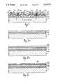
- FIG. 1is a cross-sectional view of a portion of a CMOS device on an SOI chip with an ultra-thin Si film in accordance with a LOCOS thinning embodiment the present invention.
- FIGS. 2a-2kare schematic cross-sectional process flow diagrams illustrating the major steps in processing an SOI substrate to fabricate a CMOS device in accordance with the LOCOS Thinning embodiment of the invention.
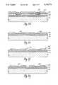
- FIGS. 3a-3gare schematic cross-sectional process flow diagrams illustrating the major steps in processing an SOI substrate to fabricate a CMOS device in accordance with an Oxide Implant embodiment of the invention.
- the preferred substrate starting structureis an SOI chip or wafer;
- the wafersmay be formed by a number of well-known techniques, such as Zone Melting and Recrystallization (ZMR) or Separation by Implanted OXygen (SIMOX).
- ZMRZone Melting and Recrystallization
- SIMOXSeparation by Implanted OXygen
- the end objectiveis to form a good quality epitaxial film of silicon 130 on a buried oxide insulator 114 supported by a bulk silicon substrate 112 (See FIG. 2a).
- Other starting substrates, such as silicon-on-sapphire (SOS),are contemplated.
- the epitaxial Si film 130is relatively thick (about 200-400 nm).
- a thin sacrificial oxide layer 140 of about 15 nmis then formed on the Si layer 130 by thermal oxidation. This film can be used as an etch stop for subsequent processing.
- a thin (100 nm) silicon nitride (Si 3 N 4 ) mask layer 150is formed over the oxide 140, preferably by low pressure chemical vapor deposition (LPCVD) (See FIG. 2b).
- the mask layer 150is coated with photoresist (not shown) and an ultra-thin or channel mask area is exposed. This mask area defines the areas where the channel regions of the silicon layer 130 must be thinned down. In addition, it also defines an optional permanent set of alignment keys (not shown) which may be used to align island definition, island implant, and the gate electrode layers.
- the nitride 150is now etched using the first sacrificial oxide 140 as the etch stop (See FIG. 2c).
- the FIG. 2c structureis coated with resist, exposed and developed in a pattern which opens up only the areas required for alignment marks and self-aligned to the nitride layer 150, are etched into the silicon film by dry etching (not shown).
- a thick oxide layer 160(200-400 nm) is grown locally by the LOCOS process in the windows 152 etched in the nitride 150.
- the total thickness of the oxideis controlled to consume a predetermined amount of the silicon film 130 (See FIG. 2d).
- the oxide 160 and nitride 150are then removed by etching to expose the thick 130' thinned silicon.
- the thinned silicon 130'is located in the channel region where the device channel is to be formed.
- a definition mask to define the regions for different transistorsis applied to the structure and the exposed silicon is etched by a dry etch to form separate regions 154 and 154' of silicon film, known as silicon islands. Each island is later converted to a transistor.
- a thin layer of a second sacrificial oxide(not shown) is then grown (8 nm). Ion implants (masked and unmasked) are made to the Si islands 154 and 154' to adjust the doping of the islands (See FIG. 2g).
- the second sacrificial oxide (8 nm) layeris etched off.
- a gate oxide 142 (10 nm or more)is then formed over the silicon islands 154 and 154'.
- Polysilicon gate (See FIG. 2i) electrodes 118 and 118'are formed over the channel regions 130' by depositing polycrystalline silicon and patterning the electrodes by photolithography and etching.
- Source and drain regions 116, 116' and 120, 120'are formed by self-aligned ion implantation (See FIG. 2j), and a passivation layer 122 of SiO 2 is formed and contact holes 123 for the source and drain regions are opened in it by photolithography and etch (See FIG. 2k).
- the final step of making metal contacts 124 and 124' to the source and drainis carried out in the conventional manner.
- the contacts 124, 124'are placed such that they fall on the thick region of the silicon islands 154, 154' (See FIG. 1).
- the precursor structurepreferably comprises a commercially available SIMOX (separation by implanted oxygen) SOI substrate consisting of bulk Si 212, an SiO 2 layer 214 and an epitaxial Si film 230, all as shown in FIG. 3a.
- SIMOXseparation by implanted oxygen
- the thickness of the silicon film 230 and of the buried oxide 214 in these substratesis each approximately equal to 250 nm.
- a thin oxide layer 240(50-60 nm) is then grown on the silicon film 230.
- a layer 250 of a masking material(silicon nitride, polysilicon, or refractory metal, such as tungsten) is deposited over the oxide layer 240 (See FIG. 3b).
- the masking layer 250is patterned by photolithography and etch techniques to obtain a pattern with two features. First, the areas where source and drain contacts of the devices are going to be formed, remain covered by the mask material 250 while the area 252 of the oxide over the channel region is exposed. The areas where alignment marks are to be engraved, are also uncovered, as in 253; leaving raised alignment mark 255 or depressed mark 253. These marks will be used in subsequent photolithography steps (See FIG. 3c).
- oxygen ionsare implanted.
- the implantis deep; penetrating to the buried oxide layer 214, as indicated by the horizontal dashes at 260L.
- the ionsare absorbed by the masking layer, as indicated by the horizontal dashed lines 260U (FIG. 3d).
- This implantationincreases the thickness of the buried oxide layer 214 in the regions not masked by the masking material.
- the silicon film thickness in these regionscorrespondingly decreases to very small value, depending upon the thickness and depth of the oxygen implant.
- the silicon film in the masked regionsi.e., the future locations of the source and drain regions and the alignment mark locations) remains of the original higher thickness.
- the implant mask 250is then selectively removed by photolithography and etching, while the alignment mark 255 is left in place.
- a high temperature annealing treatmentis then performed (1100° C. to 1300° C. for one to six hours) in an inert atmosphere to produce a stoichometric buried oxide film in the newly implanted region 260L.
- the substrate at this stagehas thick silicon regions 216 and 220, respectively, for source-drain contact regions and ultra-thin silicon regions 270 for the device channel (See FIG. 3e).
- the alignment mark 255allows further processing to be continued to fabricate CMOS devices using a fabrication process similar to the one described in FIGS. 2g-2k of the first embodiment. First, islands of silicon 230 and 230' are patterned for individual transistors using the alignment mark 255 (See FIG. 3f).
- Ion implantsare made to the silicon islands to adjust the doping.
- a gate oxide 242is formed over the islands.
- Polysilicon gate electrodes 218 and 218'are formed; n+ source and drain regions are formed in island 230 and a p+ source and drain region in island 230'.
- a passivation layer 222 of SiO 2is formed over the surface. Contact holes are made through the layer 222 and metal contacts 224 and 224' made to the thick source and drain regions of the islands, as shown in FIG. 3g.
- the embodiments shown herein of an SOI MOS device structureshould exhibit higher transconductance and operate at higher speeds than the MOS devices of comparable dimensions fabricated in uniformly ultra-thin SOI substrates because of the reduction in the resistance in series with the MOS channel.
- the inventionallows the use of extremely thin silicon film in the channel region to impart all the advantages of the ultra-thin film to the device while keeping a thicker silicon film in the source drain regions to make fabrication less complicated.
- This method of device fabricationalso produces a planar structure which, as a consequence, permits very high density of devices on a chip. This method makes possible integration of submicron transistors into large chips without a significant yield sacrifice in the complex contact making process.
- a focused beam of oxygen ionscan be used to implant oxygen in selected areas of the original SOI substrate of FIG. 3a.
- Alignment marks for aligning the ion beamcould also be pre-engraved in the original SOI substrate before implantation.
- Such a process, using a focused ion beamwould make the use of an implantation mask 250 unnecessary.
- the basic structure of the locally thinned silicon islandcan be used to make CMOS circuits with further refinements to the fabrication process, such as, LDD structure silicide conductors.
- the SOI structuremay be formed by SIMOX, or ZMR, or other known alternatives, such as wafer bonding or laser recrystallization.
Landscapes
- Engineering & Computer Science (AREA)
- Physics & Mathematics (AREA)
- Condensed Matter Physics & Semiconductors (AREA)
- General Physics & Mathematics (AREA)
- Manufacturing & Machinery (AREA)
- Computer Hardware Design (AREA)
- Microelectronics & Electronic Packaging (AREA)
- Power Engineering (AREA)
- Thin Film Transistor (AREA)
Abstract
Description
The U.S. Government has rights to this invention pursuant to the Department of the Air Force Contract No. F19628-85-C-0002.
Silicon on insulator (SOI) complementary metal oxide semiconductor (CMOS) technology has recently received a great degree of attention because it potentially offers high circuit speeds through reduction in parasitic capacitance, freedom from latch-up, higher density, and resistance to transient radiation effects. Until very recently, most SOI work has involved relatively thick (300 to 500 nm) silicon layers. Heretofore, CMOS circuits made on such layers have been found to suffer from floating body effects and short channel characteristics. These deficiencies are the main barrier to building high density, high speed SOI circuits using submicron MOS devices.
In an effort to avoid these problems inherent in such relatively thick films, researchers have turned to ultra-thin (less than 100 nm) Si films made on buried oxide insulators, i.e., SOI structures. Theoretical modeling and initial experimental work has demonstrated the advantages of fabricating CMOS devices in ultra-thin SOI films. These devices are an attractive choice for building the next generation ultra-large scale integrated (ULSI) circuits. (See "Comparison of Thin Film Transistor and SOI Technologies", H. W. Lam and M. J. Thompson (Eds), North Holland Publishing Company, New York, 1984 and M. Yoshimi, T. Wada, K. Kato, H. Tango, Technical Digest of the 1987 International Electron Devices Meeting, IEEE, Piscataway, N.J. 1987, p. 640.)
However, fabrication of CMOS devices in ultra-thin silicon films is not free from problems of its own. In addition to the difficulties associated with obtaining near defect-free SOI substrates, the next most difficult problem is the making of suitable contacts to the device in the ultra-thin source and drain regions.
When the Si film is extra-thin, the thick metallization contact film necessary for low resistance connection to the transistor source and drain regions has a tendency to dissolve the ultra-thin silicon film to which it is supposed to make contact.
If the full thickness of the ultra-thin silicon film dissolves, the contact fails. Many solutions to the problem of making contact to very shallow source and drain regions have been proposed in the prior art (W. R. Lynch, Technical Digest of the 1987 International Electron Devices Meeting, IEEE, Piscataway, N.J. 1987, p. 354). All the practical solutions involve the use of novel materials, structures, and processes resulting in fabrication complexity, increased costs and reduced yields. Moreover, all the methods used for contacts to ultra-thin source and drain regions become even more difficult to implement in the specific example of SOI substrates with a silicon thickness of less than 100 nm.
This invention provides a structure and a process which allows the use of ultra-thin silicon films in the critical (channel region) part of the MOS device, yet avoids the complications of making contacts to the ultra-thin Si film in the source and drain regions. It does so by using relatively thick, instead of ultra-thin, silicon film in the source and drain regions.
Two alternate embodiments of the invention are provided. In both embodiments, the top Si film of the SOI substrate is initially formed thick enough (approximately 250 nm or more) to provide adequately thick drain and source contact regions which will not dissolve when metallization is applied to these regions. Then, the Si channel region is thinned to an ultra-thin thickness of less than about 100 nm. In one embodiment, this channel region is thinned by a Local Oxidation of Silicon (LOCOS) process which selectively oxidizes a top volume of the silicon channel region. In the alternate solution, thinning is accomplished by oxygen ion implantation of the silicon channel region to deplete the silicon and to increase the thickness of the buried oxide by oxidizing the silicon in the channel region from below leaving a thickness of less than about 100 nm. In each case, the source and drain regions remain relatively thick for good ohmic contact formation.
FIG. 1 is a cross-sectional view of a portion of a CMOS device on an SOI chip with an ultra-thin Si film in accordance with a LOCOS thinning embodiment the present invention.
FIGS. 2a-2k are schematic cross-sectional process flow diagrams illustrating the major steps in processing an SOI substrate to fabricate a CMOS device in accordance with the LOCOS Thinning embodiment of the invention.
FIGS. 3a-3g are schematic cross-sectional process flow diagrams illustrating the major steps in processing an SOI substrate to fabricate a CMOS device in accordance with an Oxide Implant embodiment of the invention.
Referring now to FIGS. 1 and 2a-2k, a LOCOS thinning embodiment of the invention will now be described in detail. It should be noted that in all embodiments, the preferred substrate starting structure is an SOI chip or wafer; The wafers may be formed by a number of well-known techniques, such as Zone Melting and Recrystallization (ZMR) or Separation by Implanted OXygen (SIMOX). The end objective is to form a good quality epitaxial film ofsilicon 130 on a buriedoxide insulator 114 supported by a bulk silicon substrate 112 (See FIG. 2a). Other starting substrates, such as silicon-on-sapphire (SOS), are contemplated. Initially, theepitaxial Si film 130 is relatively thick (about 200-400 nm). A thinsacrificial oxide layer 140 of about 15 nm is then formed on theSi layer 130 by thermal oxidation. This film can be used as an etch stop for subsequent processing.
Next, a thin (100 nm) silicon nitride (Si3 N4)mask layer 150 is formed over theoxide 140, preferably by low pressure chemical vapor deposition (LPCVD) (See FIG. 2b). Themask layer 150 is coated with photoresist (not shown) and an ultra-thin or channel mask area is exposed. This mask area defines the areas where the channel regions of thesilicon layer 130 must be thinned down. In addition, it also defines an optional permanent set of alignment keys (not shown) which may be used to align island definition, island implant, and the gate electrode layers. Thenitride 150 is now etched using the firstsacrificial oxide 140 as the etch stop (See FIG. 2c). Optionally, at this point, the FIG. 2c structure is coated with resist, exposed and developed in a pattern which opens up only the areas required for alignment marks and self-aligned to thenitride layer 150, are etched into the silicon film by dry etching (not shown).
All the resist is then cleaned off the substrate and a thick oxide layer 160 (200-400 nm) is grown locally by the LOCOS process in thewindows 152 etched in thenitride 150. The total thickness of the oxide is controlled to consume a predetermined amount of the silicon film 130 (See FIG. 2d).
Theoxide 160 andnitride 150 are then removed by etching to expose the thick 130' thinned silicon. The thinned silicon 130' is located in the channel region where the device channel is to be formed. A definition mask to define the regions for different transistors is applied to the structure and the exposed silicon is etched by a dry etch to formseparate regions 154 and 154' of silicon film, known as silicon islands. Each island is later converted to a transistor. A thin layer of a second sacrificial oxide (not shown) is then grown (8 nm). Ion implants (masked and unmasked) are made to theSi islands 154 and 154' to adjust the doping of the islands (See FIG. 2g). The second sacrificial oxide (8 nm) layer is etched off. A gate oxide 142 (10 nm or more) is then formed over thesilicon islands 154 and 154'. Polysilicon gate (See FIG. 2i)electrodes 118 and 118' are formed over the channel regions 130' by depositing polycrystalline silicon and patterning the electrodes by photolithography and etching. Source anddrain regions passivation layer 122 of SiO2 is formed andcontact holes 123 for the source and drain regions are opened in it by photolithography and etch (See FIG. 2k).
The final step of makingmetal contacts 124 and 124' to the source and drain is carried out in the conventional manner. Thecontacts 124, 124' are placed such that they fall on the thick region of thesilicon islands 154, 154' (See FIG. 1).
The above process allows fabrication of high speed, submicron SOI CMOS devices with ultra-thin silicon channels using proven and manufacturable processing steps. Local oxidation with nitride masks and making contacts to 300 nm of silicon film are well proven and manufacturable processes. As a by-product, this method allows the use of good quality, thicker SOI films avoiding the necessity to develop ultra-thin SOI substrate materials.
The alternate embodiment, using oxygen ion implantation for channel thinning, will now be described in connection with FIGS. 3a-3d.
The precursor structure preferably comprises a commercially available SIMOX (separation by implanted oxygen) SOI substrate consisting ofbulk Si 212, an SiO2 layer 214 and anepitaxial Si film 230, all as shown in FIG. 3a. The thickness of thesilicon film 230 and of the buriedoxide 214 in these substrates is each approximately equal to 250 nm.
A thin oxide layer 240 (50-60 nm) is then grown on thesilicon film 230. Alayer 250 of a masking material (silicon nitride, polysilicon, or refractory metal, such as tungsten) is deposited over the oxide layer 240 (See FIG. 3b).
Themasking layer 250 is patterned by photolithography and etch techniques to obtain a pattern with two features. First, the areas where source and drain contacts of the devices are going to be formed, remain covered by themask material 250 while thearea 252 of the oxide over the channel region is exposed. The areas where alignment marks are to be engraved, are also uncovered, as in 253; leaving raisedalignment mark 255 ordepressed mark 253. These marks will be used in subsequent photolithography steps (See FIG. 3c).
Next, oxygen ions are implanted. In the exposedregions oxide layer 214, as indicated by the horizontal dashes at 260L. In the unexposed regions, the ions are absorbed by the masking layer, as indicated by the horizontal dashedlines 260U (FIG. 3d). This implantation increases the thickness of the buriedoxide layer 214 in the regions not masked by the masking material. The silicon film thickness in these regions correspondingly decreases to very small value, depending upon the thickness and depth of the oxygen implant. The silicon film in the masked regions (i.e., the future locations of the source and drain regions and the alignment mark locations) remains of the original higher thickness.
Theimplant mask 250 is then selectively removed by photolithography and etching, while thealignment mark 255 is left in place. A high temperature annealing treatment is then performed (1100° C. to 1300° C. for one to six hours) in an inert atmosphere to produce a stoichometric buried oxide film in the newly implantedregion 260L.
The substrate at this stage hasthick silicon regions ultra-thin silicon regions 270 for the device channel (See FIG. 3e). Thealignment mark 255 allows further processing to be continued to fabricate CMOS devices using a fabrication process similar to the one described in FIGS. 2g-2k of the first embodiment. First, islands ofsilicon 230 and 230' are patterned for individual transistors using the alignment mark 255 (See FIG. 3f).
Ion implants are made to the silicon islands to adjust the doping. Agate oxide 242 is formed over the islands.Polysilicon gate electrodes 218 and 218' are formed; n+ source and drain regions are formed inisland 230 and a p+ source and drain region in island 230'. Apassivation layer 222 of SiO2 is formed over the surface. Contact holes are made through thelayer 222 andmetal contacts 224 and 224' made to the thick source and drain regions of the islands, as shown in FIG. 3g.
The embodiments shown herein of an SOI MOS device structure should exhibit higher transconductance and operate at higher speeds than the MOS devices of comparable dimensions fabricated in uniformly ultra-thin SOI substrates because of the reduction in the resistance in series with the MOS channel. Yet, the invention allows the use of extremely thin silicon film in the channel region to impart all the advantages of the ultra-thin film to the device while keeping a thicker silicon film in the source drain regions to make fabrication less complicated. This method of device fabrication also produces a planar structure which, as a consequence, permits very high density of devices on a chip. This method makes possible integration of submicron transistors into large chips without a significant yield sacrifice in the complex contact making process.
The above described embodiments are preferred. Other configurations and modifications will now be apparent based upon the present description. Thus, the invention should only be limited in scope by the language of the following claims and equivalents. For example, it is contemplated that alternatively, a focused beam of oxygen ions can be used to implant oxygen in selected areas of the original SOI substrate of FIG. 3a. Alignment marks for aligning the ion beam could also be pre-engraved in the original SOI substrate before implantation. Such a process, using a focused ion beam would make the use of animplantation mask 250 unnecessary. The basic structure of the locally thinned silicon island can be used to make CMOS circuits with further refinements to the fabrication process, such as, LDD structure silicide conductors. The SOI structure may be formed by SIMOX, or ZMR, or other known alternatives, such as wafer bonding or laser recrystallization.
Claims (10)
1. The method of forming a device with silicon channel regions between silicon source regions and silicon drain regions of an epitaxial silicon film on insulator substrate comprising the steps of:
a) forming a protective layer over the silicon film;
b) forming a mask layer over the protective layer;
c) removing regions of the mask layer to form openings overlying the channel regions;
d) thinning the silicon regions underlying the openings leaving the source and drain regions on either side the same thickness as the original silicon film.
2. The method of claim 1 including the step of removing the remaining mask layer and forming metal contacts on the source and drain regions and a polysilicon gate electrode on the channel regions.
3. The method of claim 1 wherein the silicon regions are thinned by local oxidation of a surface volume of the silicon underlying the openings.
4. The method of clam 1 wherein the silicon regions are thinned by implantation of oxygen ions in the silicon underlying the openings.
5. The method of claim 1 wherein the silicon-on-insulator substrate is formed by zone melt recrystallization of silicon to form a relatively thick film of epitaxial silicon on a buried oxide insulator on a silicon substrate.
6. The method of claim 1 wherein the substrate is formed by separating the epitaxial silicon film from an underlying silicon base by oxide ion implantation of a volume of the silicon base structure.
7. A method for forming a transistor in an epitaxial silicon layer on insulator on silicon substrate comprising the steps of:
a) forming a etch stop layer on said silicon layer;
b) forming a mask layer on said etch stop layer;
c) removing portions of said mask layer to form openings in locations where transistor channel regions are to be formed in said silicon;
d) oxidizing said silicon underlying said openings to thin said silicon in said channel regions;
e) forming a gate dielectric layer over the silicon layer;
f) forming a gate electrode over the channel regions;
g) doping the silicon in regions on either side of the gate electrodes to form respective source and drain regions;
h) forming metal contacts on the source and drain regions.
8. The method of forming a device with silicon channel regions disposed between laterally adjacent silicon source regions and silicon drain regions of an epitaxial silicon film on insulator substrate comprising the steps of:
a) forming a protective layer over the silicon film;
b) forming a mask layer over the protective layer;
c) removing regions of the mask layer to form openings where the channel regions are to be located;
d) thinning the silicon regions underlying the openings leaving thick regions on either side of thin regions where the source and drain regions are to be located;
e) removing the mask layer and protective layer and doping the thick regions with a first type conductivity donor and the thin regions between with a second type conductivity donor of opposite conductivity to the first;
f) forming an insulator over the thin and thick regions;
g) forming a gate electrode over the insulator opposite the thin region;
h) forming openings in said insulator to said thick regions; and
i) forming contacts in said openings.
9. The method of claim 8 wherein the silicon regions are thinned by local oxidation of a surface volume of silicon underlying the openings.
10. The method of claim 8 wherein the silicon regions are thinned by implantation of oxygen ions in the silicon underlying the openings.
Priority Applications (1)
| Application Number | Priority Date | Filing Date | Title |
|---|---|---|---|
| US07/326,169US5116771A (en) | 1989-03-20 | 1989-03-20 | Thick contacts for ultra-thin silicon on insulator films |
Applications Claiming Priority (1)
| Application Number | Priority Date | Filing Date | Title |
|---|---|---|---|
| US07/326,169US5116771A (en) | 1989-03-20 | 1989-03-20 | Thick contacts for ultra-thin silicon on insulator films |
Publications (1)
| Publication Number | Publication Date |
|---|---|
| US5116771Atrue US5116771A (en) | 1992-05-26 |
Family
ID=23271085
Family Applications (1)
| Application Number | Title | Priority Date | Filing Date |
|---|---|---|---|
| US07/326,169Expired - LifetimeUS5116771A (en) | 1989-03-20 | 1989-03-20 | Thick contacts for ultra-thin silicon on insulator films |
Country Status (1)
| Country | Link |
|---|---|
| US (1) | US5116771A (en) |
Cited By (49)
| Publication number | Priority date | Publication date | Assignee | Title |
|---|---|---|---|---|
| US5206749A (en)* | 1990-12-31 | 1993-04-27 | Kopin Corporation | Liquid crystal display having essentially single crystal transistors pixels and driving circuits |
| US5294555A (en)* | 1982-04-13 | 1994-03-15 | Seiko Epson Corporation | Method of manufacturing thin film transistor and active matrix assembly including same |
| EP0635880A1 (en)* | 1993-07-22 | 1995-01-25 | Commissariat A L'energie Atomique | Method of manufacturing a transistor using silicon on insulator technology |
| EP0637061A1 (en)* | 1993-06-29 | 1995-02-01 | Digital Equipment Corporation | Threshold optimization for SOI transistors through use of negative charge in the gate oxide |
| US5397718A (en)* | 1992-02-21 | 1995-03-14 | Matsushita Electric Industrial Co., Ltd. | Method of manufacturing thin film transistor |
| US5436184A (en)* | 1991-09-20 | 1995-07-25 | Mitsubishi Denki Kabushiki Kaisha | Thin film transistor and manufacturing method thereof |
| US5488005A (en)* | 1994-05-06 | 1996-01-30 | Samsung Electronics Co., Ltd. | Process for manufacturing an offset gate structure thin film transistor |
| US5489792A (en)* | 1994-04-07 | 1996-02-06 | Regents Of The University Of California | Silicon-on-insulator transistors having improved current characteristics and reduced electrostatic discharge susceptibility |
| EP0704892A3 (en)* | 1994-09-30 | 1996-11-13 | Nippon Steel Corp | Method of manufacturing a semiconductor substrate |
| EP0687002A3 (en)* | 1994-06-03 | 1996-11-13 | Komatsu Denshi Kinzoku Kk | Method for manufacturing a semiconductor device of the SOI type |
| EP0675534A3 (en)* | 1994-03-23 | 1996-11-13 | Komatsu Denshi Kinzoku Kk | SOI substrate and method of manufacturing the substrate. |
| EP0615282A3 (en)* | 1993-03-10 | 1996-12-11 | Samsung Electronics Co Ltd | Process for the production of MOSFETs with a channel cut from the well. |
| US5599728A (en)* | 1994-04-07 | 1997-02-04 | Regents Of The University Of California | Method of fabricating a self-aligned high speed MOSFET device |
| US5637513A (en)* | 1994-07-08 | 1997-06-10 | Nec Corporation | Fabrication method of semiconductor device with SOI structure |
| US5726081A (en)* | 1995-10-18 | 1998-03-10 | United Microelectronics Corp. | Method of fabricating metal contact of ultra-large-scale integration metal-oxide semiconductor field effect transistor with silicon-on-insulator structure |
| US5792678A (en)* | 1996-05-02 | 1998-08-11 | Motorola, Inc. | Method for fabricating a semiconductor on insulator device |
| US5879976A (en)* | 1996-08-22 | 1999-03-09 | Sharp Kabushiki Kaisha | Thin film transistor and method for producing the same |
| US5882958A (en)* | 1997-09-03 | 1999-03-16 | Wanlass; Frank M. | Damascene method for source drain definition of silicon on insulator MOS transistors |
| US5930642A (en)* | 1997-06-09 | 1999-07-27 | Advanced Micro Devices, Inc. | Transistor with buried insulative layer beneath the channel region |
| US5976924A (en)* | 1997-12-30 | 1999-11-02 | Advanced Micro Devices, Inc. | Method of making a self-aligned disposable gate electrode for advanced CMOS design |
| US6048756A (en)* | 1997-07-31 | 2000-04-11 | Electronics And Telecommunications Research Institute | Method for making a silicon-on-insulator MOS transistor using a selective SiGe epitaxy |
| US6100147A (en)* | 1998-04-16 | 2000-08-08 | Advanced Micro Devices, Inc. | Method for manufacturing a high performance transistor with self-aligned dopant profile |
| US6150696A (en)* | 1997-10-06 | 2000-11-21 | Mitsubishi Denki Kabushiki Kaisha | Semiconductor substrate and method of fabricating semiconductor device |
| US6204100B1 (en)* | 1998-02-12 | 2001-03-20 | Hyundai Electronics Industries Co., Ltd. | CMOS device and method for fabricating the same |
| US6214684B1 (en)* | 1995-09-29 | 2001-04-10 | Canon Kabushiki Kaisha | Method of forming a semiconductor device using an excimer laser to selectively form the gate insulator |
| US6261886B1 (en)* | 1998-08-04 | 2001-07-17 | Texas Instruments Incorporated | Increased gate to body coupling and application to DRAM and dynamic circuits |
| US6287901B1 (en)* | 2000-01-05 | 2001-09-11 | International Business Machines Corporation | Method and semiconductor structure for implementing dual plane body contacts for silicon-on-insulator (SOI) transistors |
| US6329265B1 (en)* | 1991-11-20 | 2001-12-11 | Canon Kabushiki Kaisha | Method of making a semiconductor device using processing from both sides of a workpiece |
| US6426500B1 (en)* | 1998-11-02 | 2002-07-30 | Mosel Vitelic Inc. | Method for protecting a specific region in a sample applied in preparing an ultra-thin specimen |
| US6514803B1 (en)* | 1993-12-22 | 2003-02-04 | Tdk Corporation | Process for making an amorphous silicon thin film semiconductor device |
| US20030027400A1 (en)* | 2001-07-31 | 2003-02-06 | Samsung Electronics Co., Ltd. | SOI structure and method of producing same |
| US20030170938A1 (en)* | 2002-03-11 | 2003-09-11 | Nec Corporation | Thin film semiconductor device and method for manufacturing same |
| US6709913B2 (en)* | 2001-09-04 | 2004-03-23 | Sharp Laboratories Of America, Inc. | Method for adjusting ultra-thin SOI MOS transistor threshold voltages |
| US6870225B2 (en) | 2001-11-02 | 2005-03-22 | International Business Machines Corporation | Transistor structure with thick recessed source/drain structures and fabrication process of same |
| US20050110091A1 (en)* | 1992-08-27 | 2005-05-26 | Semiconductor Energy Laboratory Co., Ltd. | Semiconductor device and method for forming the same |
| US20060014389A1 (en)* | 2004-07-14 | 2006-01-19 | Jun Osanai | Method of manufacturing semiconductor device |
| US20060084249A1 (en)* | 2004-10-19 | 2006-04-20 | Kabushiki Kaisha Toshiba | Method for manufacturing a hybrid semiconductor wafer having a buried oxide film |
| US20060175659A1 (en)* | 2005-02-07 | 2006-08-10 | International Business Machines Corporation | A cmos structure for body ties in ultra-thin soi (utsoi) substrates |
| US20060223279A1 (en)* | 2005-04-01 | 2006-10-05 | Micron Technology, Inc. | Methods of forming trench isolation in the fabrication of integrated circuitry and methods of fabricating integrated circuitry |
| US20060276040A1 (en)* | 2005-02-17 | 2006-12-07 | Abraham Margaret H | Ion implanted microscale and nanoscale device method |
| US20070063287A1 (en)* | 2005-09-16 | 2007-03-22 | Renesas Technology Corp. | Semiconductor device |
| US20090026545A1 (en)* | 2007-07-23 | 2009-01-29 | Advanced Micro Devices, Inc. | Integrated circuit employing variable thickness film |
| US20090039426A1 (en)* | 2007-08-10 | 2009-02-12 | International Business Machines Corporation | Extremely-thin silicon-on-insulator transistor with raised source/drain |
| US7759205B1 (en)* | 2009-01-16 | 2010-07-20 | Advanced Micro Devices, Inc. | Methods for fabricating semiconductor devices minimizing under-oxide regrowth |
| US20110092061A1 (en)* | 2009-10-20 | 2011-04-21 | Yunjun Ho | Methods of Forming Silicon Oxides and Methods of Forming Interlevel Dielectrics |
| EP2757580A1 (en)* | 2013-01-22 | 2014-07-23 | Nxp B.V. | Bipolar cmos dmos (bcd) processes |
| US9570437B2 (en) | 2014-01-09 | 2017-02-14 | Nxp B.V. | Semiconductor die, integrated circuits and driver circuits, and methods of maufacturing the same |
| WO2018163605A1 (en)* | 2017-03-08 | 2018-09-13 | ソニーセミコンダクタソリューションズ株式会社 | Semiconductor device and method for manufacturing semiconductor device |
| US11699757B2 (en)* | 2014-01-31 | 2023-07-11 | Stmicroelectronics, Inc. | High dose implantation for ultrathin semiconductor-on-insulator substrates |
Citations (7)
| Publication number | Priority date | Publication date | Assignee | Title |
|---|---|---|---|---|
| US4183134A (en)* | 1977-02-15 | 1980-01-15 | Westinghouse Electric Corp. | High yield processing for silicon-on-sapphire CMOS integrated circuits |
| JPS5568651A (en)* | 1978-11-20 | 1980-05-23 | Nippon Telegr & Teleph Corp <Ntt> | Manufacturing method of semiconductor device |
| JPS5710266A (en)* | 1980-06-23 | 1982-01-19 | Fujitsu Ltd | Mis field effect semiconductor device |
| JPS60117782A (en)* | 1983-11-30 | 1985-06-25 | Fujitsu Ltd | Mos type field effect transistor and manufacture thereof |
| US4700461A (en)* | 1986-09-29 | 1987-10-20 | Massachusetts Institute Of Technology | Process for making junction field-effect transistors |
| JPS62296563A (en)* | 1986-06-17 | 1987-12-23 | Matsushita Electronics Corp | Insulated-gate transistor and manufacture thereof |
| US4717686A (en)* | 1985-06-03 | 1988-01-05 | Siemens Aktiengesellschaft | Method for the simultaneous manufacture of bipolar and complementary MOS transistors on a common silicon substrate |
- 1989
- 1989-03-20USUS07/326,169patent/US5116771A/ennot_activeExpired - Lifetime
Patent Citations (7)
| Publication number | Priority date | Publication date | Assignee | Title |
|---|---|---|---|---|
| US4183134A (en)* | 1977-02-15 | 1980-01-15 | Westinghouse Electric Corp. | High yield processing for silicon-on-sapphire CMOS integrated circuits |
| JPS5568651A (en)* | 1978-11-20 | 1980-05-23 | Nippon Telegr & Teleph Corp <Ntt> | Manufacturing method of semiconductor device |
| JPS5710266A (en)* | 1980-06-23 | 1982-01-19 | Fujitsu Ltd | Mis field effect semiconductor device |
| JPS60117782A (en)* | 1983-11-30 | 1985-06-25 | Fujitsu Ltd | Mos type field effect transistor and manufacture thereof |
| US4717686A (en)* | 1985-06-03 | 1988-01-05 | Siemens Aktiengesellschaft | Method for the simultaneous manufacture of bipolar and complementary MOS transistors on a common silicon substrate |
| JPS62296563A (en)* | 1986-06-17 | 1987-12-23 | Matsushita Electronics Corp | Insulated-gate transistor and manufacture thereof |
| US4700461A (en)* | 1986-09-29 | 1987-10-20 | Massachusetts Institute Of Technology | Process for making junction field-effect transistors |
Non-Patent Citations (18)
| Title |
|---|
| "A High Performance Submicrometer CMOS/SOI Technology Using Ultrathin Silicon Films on SIMOX", Vasudev et al., pp. 61-62, Technical Digest of 1988 Symp. on VLSI Technol., May 1988, IEEE. |
| "A Metal-Gate Self-Aligned MOSFET Using Nitride Oxide", Schmidt, et al., IEEE Transactions on Electron Devices, vol. ED-32, No. 3, Mar. 1985, pp. 643-648. |
| "Application of Selective Silicon Epitaxial Growth for CMOS Technology", Nagao et al., IEEE Transactions on Electron Devices, vol. ED-33, No. 11, Nov. 1986, pp. 1738-1744. |
| "High Performance SOIMOSFET Using Ultra-Thin SOI Film", Yoshimi et al., IEDM 87, pp. 640-643. |
| "Local Oxidation of Silicon and Its Application in Semiconductor-Device Technology", Appels et al., Phillips Res. Repts 25, pp. 118-132, 1970. |
| "Local Oxidation of Silicon; New Technological Aspects", Appels, et al., Philipps. Res. Repts 26, 157-165, 1971. |
| "Novel SOI CMOS Design Using Ultra Thin Near Intrinsic Substrate", Malhi et al., IEEE 1982, pp. 107-110. |
| "Rapid Thermal Growth of Thin Silicon Dielectrics for ULSI Applications", J. Nulman, Proc. 1st Int'nl Symp on ULSI Science and Technology, Proc. vol. 87-11, Electrochemical Society, (1987), p. 141. |
| "Self-Aligned Contact Schemes for Source-Drains in Submicron Devices", W. T. Lynch, IEDM 87, pp. 354-357. |
| A High Performance Submicrometer CMOS/SOI Technology Using Ultrathin Silicon Films on SIMOX , Vasudev et al., pp. 61 62, Technical Digest of 1988 Symp. on VLSI Technol., May 1988, IEEE.* |
| A Metal Gate Self Aligned MOSFET Using Nitride Oxide , Schmidt, et al., IEEE Transactions on Electron Devices, vol. ED 32, No. 3, Mar. 1985, pp. 643 648.* |
| Application of Selective Silicon Epitaxial Growth for CMOS Technology , Nagao et al., IEEE Transactions on Electron Devices, vol. ED 33, No. 11, Nov. 1986, pp. 1738 1744.* |
| High Performance SOIMOSFET Using Ultra Thin SOI Film , Yoshimi et al., IEDM 87, pp. 640 643.* |
| Local Oxidation of Silicon and Its Application in Semiconductor Device Technology , Appels et al., Phillips Res. Repts 25, pp. 118 132, 1970.* |
| Local Oxidation of Silicon; New Technological Aspects , Appels, et al., Philipps. Res. Repts 26, 157 165, 1971.* |
| Novel SOI CMOS Design Using Ultra Thin Near Intrinsic Substrate , Malhi et al., IEEE 1982, pp. 107 110.* |
| Rapid Thermal Growth of Thin Silicon Dielectrics for ULSI Applications , J. Nulman, Proc. 1st Int nl Symp on ULSI Science and Technology, Proc. vol. 87 11, Electrochemical Society, (1987), p. 141.* |
| Self Aligned Contact Schemes for Source Drains in Submicron Devices , W. T. Lynch, IEDM 87, pp. 354 357.* |
Cited By (83)
| Publication number | Priority date | Publication date | Assignee | Title |
|---|---|---|---|---|
| US5294555A (en)* | 1982-04-13 | 1994-03-15 | Seiko Epson Corporation | Method of manufacturing thin film transistor and active matrix assembly including same |
| US5206749A (en)* | 1990-12-31 | 1993-04-27 | Kopin Corporation | Liquid crystal display having essentially single crystal transistors pixels and driving circuits |
| US5436184A (en)* | 1991-09-20 | 1995-07-25 | Mitsubishi Denki Kabushiki Kaisha | Thin film transistor and manufacturing method thereof |
| US6329265B1 (en)* | 1991-11-20 | 2001-12-11 | Canon Kabushiki Kaisha | Method of making a semiconductor device using processing from both sides of a workpiece |
| US5397718A (en)* | 1992-02-21 | 1995-03-14 | Matsushita Electric Industrial Co., Ltd. | Method of manufacturing thin film transistor |
| US20050110091A1 (en)* | 1992-08-27 | 2005-05-26 | Semiconductor Energy Laboratory Co., Ltd. | Semiconductor device and method for forming the same |
| US7329906B2 (en) | 1992-08-27 | 2008-02-12 | Semiconductor Energy Laboratory Co., Ltd. | Semiconductor device and method for forming the same |
| US7416907B2 (en) | 1992-08-27 | 2008-08-26 | Semiconductor Energy Laboratory Co., Ltd. | Semiconductor device and method for forming the same |
| EP0615282A3 (en)* | 1993-03-10 | 1996-12-11 | Samsung Electronics Co Ltd | Process for the production of MOSFETs with a channel cut from the well. |
| EP0637061A1 (en)* | 1993-06-29 | 1995-02-01 | Digital Equipment Corporation | Threshold optimization for SOI transistors through use of negative charge in the gate oxide |
| US5439836A (en)* | 1993-07-22 | 1995-08-08 | Commissariat A L'energie Atomique | Method for producing a silicon technology transistor on a nonconductor |
| EP0635880A1 (en)* | 1993-07-22 | 1995-01-25 | Commissariat A L'energie Atomique | Method of manufacturing a transistor using silicon on insulator technology |
| FR2708142A1 (en)* | 1993-07-22 | 1995-01-27 | Commissariat Energie Atomique | Method of manufacturing a transistor in silicon on insulator technology. |
| US6514803B1 (en)* | 1993-12-22 | 2003-02-04 | Tdk Corporation | Process for making an amorphous silicon thin film semiconductor device |
| US5918136A (en)* | 1994-03-23 | 1999-06-29 | Komatsu Electronic Metals Co., Ltd., | SOI substrate and method of producing the same |
| EP0675534A3 (en)* | 1994-03-23 | 1996-11-13 | Komatsu Denshi Kinzoku Kk | SOI substrate and method of manufacturing the substrate. |
| US5982003A (en)* | 1994-04-07 | 1999-11-09 | The Regents Of The University Of California | Silicon-on-insulator transistors having improved current characteristics and reduced electrostatic discharge susceptibility |
| US6300649B1 (en)* | 1994-04-07 | 2001-10-09 | The Regents Of The University Of California | Silicon-on-insulator transistors having improved current characteristics and reduced electrostatic discharge susceptibility |
| US6121077A (en)* | 1994-04-07 | 2000-09-19 | The Regents Of The University Of California | Silicon-on-insulator transistors having improved current characteristics and reduced electrostatic discharge susceptibility |
| US5489792A (en)* | 1994-04-07 | 1996-02-06 | Regents Of The University Of California | Silicon-on-insulator transistors having improved current characteristics and reduced electrostatic discharge susceptibility |
| US5599728A (en)* | 1994-04-07 | 1997-02-04 | Regents Of The University Of California | Method of fabricating a self-aligned high speed MOSFET device |
| US5488005A (en)* | 1994-05-06 | 1996-01-30 | Samsung Electronics Co., Ltd. | Process for manufacturing an offset gate structure thin film transistor |
| EP0687002A3 (en)* | 1994-06-03 | 1996-11-13 | Komatsu Denshi Kinzoku Kk | Method for manufacturing a semiconductor device of the SOI type |
| SG93171A1 (en)* | 1994-06-03 | 2002-12-17 | Komatsu Denshi Kinzoku Kk | Producing method of semiconductor device |
| US5637513A (en)* | 1994-07-08 | 1997-06-10 | Nec Corporation | Fabrication method of semiconductor device with SOI structure |
| EP0704892A3 (en)* | 1994-09-30 | 1996-11-13 | Nippon Steel Corp | Method of manufacturing a semiconductor substrate |
| US6214684B1 (en)* | 1995-09-29 | 2001-04-10 | Canon Kabushiki Kaisha | Method of forming a semiconductor device using an excimer laser to selectively form the gate insulator |
| US5726081A (en)* | 1995-10-18 | 1998-03-10 | United Microelectronics Corp. | Method of fabricating metal contact of ultra-large-scale integration metal-oxide semiconductor field effect transistor with silicon-on-insulator structure |
| US5792678A (en)* | 1996-05-02 | 1998-08-11 | Motorola, Inc. | Method for fabricating a semiconductor on insulator device |
| US5879976A (en)* | 1996-08-22 | 1999-03-09 | Sharp Kabushiki Kaisha | Thin film transistor and method for producing the same |
| US5930642A (en)* | 1997-06-09 | 1999-07-27 | Advanced Micro Devices, Inc. | Transistor with buried insulative layer beneath the channel region |
| US6048756A (en)* | 1997-07-31 | 2000-04-11 | Electronics And Telecommunications Research Institute | Method for making a silicon-on-insulator MOS transistor using a selective SiGe epitaxy |
| US5882958A (en)* | 1997-09-03 | 1999-03-16 | Wanlass; Frank M. | Damascene method for source drain definition of silicon on insulator MOS transistors |
| US6335267B1 (en) | 1997-10-06 | 2002-01-01 | Mitsubishi Denki Kabushiki Kaisha | Semiconductor substrate and method of fabricating semiconductor device |
| US6150696A (en)* | 1997-10-06 | 2000-11-21 | Mitsubishi Denki Kabushiki Kaisha | Semiconductor substrate and method of fabricating semiconductor device |
| US5976924A (en)* | 1997-12-30 | 1999-11-02 | Advanced Micro Devices, Inc. | Method of making a self-aligned disposable gate electrode for advanced CMOS design |
| US6204100B1 (en)* | 1998-02-12 | 2001-03-20 | Hyundai Electronics Industries Co., Ltd. | CMOS device and method for fabricating the same |
| US6531742B2 (en) | 1998-02-12 | 2003-03-11 | Hyundai Electronics Industries Co., Ltd. | Method of forming CMOS device |
| US6100147A (en)* | 1998-04-16 | 2000-08-08 | Advanced Micro Devices, Inc. | Method for manufacturing a high performance transistor with self-aligned dopant profile |
| US6261886B1 (en)* | 1998-08-04 | 2001-07-17 | Texas Instruments Incorporated | Increased gate to body coupling and application to DRAM and dynamic circuits |
| US6426500B1 (en)* | 1998-11-02 | 2002-07-30 | Mosel Vitelic Inc. | Method for protecting a specific region in a sample applied in preparing an ultra-thin specimen |
| US6528853B2 (en) | 2000-01-05 | 2003-03-04 | International Business Machines Corporation | Method and semiconductor structure for implementing dual plane body contacts for silicon-on-insulator (SOI) transistors |
| US6287901B1 (en)* | 2000-01-05 | 2001-09-11 | International Business Machines Corporation | Method and semiconductor structure for implementing dual plane body contacts for silicon-on-insulator (SOI) transistors |
| US6656806B2 (en)* | 2001-07-31 | 2003-12-02 | Samsung Electronics Co., Ltd. | SOI structure and method of producing same |
| US20040056309A1 (en)* | 2001-07-31 | 2004-03-25 | Samsung Electronics Co., Ltd. | SOI structure and method of producing same |
| US20030027400A1 (en)* | 2001-07-31 | 2003-02-06 | Samsung Electronics Co., Ltd. | SOI structure and method of producing same |
| US6709913B2 (en)* | 2001-09-04 | 2004-03-23 | Sharp Laboratories Of America, Inc. | Method for adjusting ultra-thin SOI MOS transistor threshold voltages |
| US7132339B2 (en) | 2001-11-02 | 2006-11-07 | International Business Machines Corporation | Transistor structure with thick recessed source/drain structures and fabrication process of same |
| US6870225B2 (en) | 2001-11-02 | 2005-03-22 | International Business Machines Corporation | Transistor structure with thick recessed source/drain structures and fabrication process of same |
| US20050101072A1 (en)* | 2001-11-02 | 2005-05-12 | Andres Bryant | Transistor structure with thick recessed source/drain structures and fabrication process of same |
| US20050045883A1 (en)* | 2002-03-11 | 2005-03-03 | Nec Corporation | Thin film semiconductor device and method for manufacturing same |
| US7109554B2 (en) | 2002-03-11 | 2006-09-19 | Nec Corporation | Thin film semiconductor device and method for manufacturing same |
| US20060261339A1 (en)* | 2002-03-11 | 2006-11-23 | Nec Corporation | Thin film semiconductor device and method for manufacturing same |
| US6972221B2 (en)* | 2002-03-11 | 2005-12-06 | Nec Corporation | Thin film semiconductor device and method for manufacturing same |
| US20030170938A1 (en)* | 2002-03-11 | 2003-09-11 | Nec Corporation | Thin film semiconductor device and method for manufacturing same |
| US20060014389A1 (en)* | 2004-07-14 | 2006-01-19 | Jun Osanai | Method of manufacturing semiconductor device |
| US20060084249A1 (en)* | 2004-10-19 | 2006-04-20 | Kabushiki Kaisha Toshiba | Method for manufacturing a hybrid semiconductor wafer having a buried oxide film |
| US20060175659A1 (en)* | 2005-02-07 | 2006-08-10 | International Business Machines Corporation | A cmos structure for body ties in ultra-thin soi (utsoi) substrates |
| US7687365B2 (en) | 2005-02-07 | 2010-03-30 | International Business Machines Corporation | CMOS structure for body ties in ultra-thin SOI (UTSOI) substrates |
| US20080248615A1 (en)* | 2005-02-07 | 2008-10-09 | International Business Machines Corporation | Cmos structure for body ties in ultra-thin soi (utsoi) substrates |
| US20060276040A1 (en)* | 2005-02-17 | 2006-12-07 | Abraham Margaret H | Ion implanted microscale and nanoscale device method |
| US7419917B2 (en)* | 2005-02-17 | 2008-09-02 | The Aerospace Corporation | Ion implanted microscale and nanoscale device method |
| US8012847B2 (en)* | 2005-04-01 | 2011-09-06 | Micron Technology, Inc. | Methods of forming trench isolation in the fabrication of integrated circuitry and methods of fabricating integrated circuitry |
| US8349699B2 (en) | 2005-04-01 | 2013-01-08 | Micron Technology, Inc. | Methods of forming trench isolation in the fabrication of integrated circuitry and methods of fabricating integrated circuitry |
| US20060223279A1 (en)* | 2005-04-01 | 2006-10-05 | Micron Technology, Inc. | Methods of forming trench isolation in the fabrication of integrated circuitry and methods of fabricating integrated circuitry |
| US20070063287A1 (en)* | 2005-09-16 | 2007-03-22 | Renesas Technology Corp. | Semiconductor device |
| US8106449B2 (en)* | 2005-09-16 | 2012-01-31 | Renesas Electronics Corporation | Semiconductor device |
| US9640666B2 (en) | 2007-07-23 | 2017-05-02 | GlobalFoundries, Inc. | Integrated circuit employing variable thickness film |
| US20090026545A1 (en)* | 2007-07-23 | 2009-01-29 | Advanced Micro Devices, Inc. | Integrated circuit employing variable thickness film |
| US7871869B2 (en) | 2007-08-10 | 2011-01-18 | International Business Machines Corporation | Extremely-thin silicon-on-insulator transistor with raised source/drain |
| US20090039426A1 (en)* | 2007-08-10 | 2009-02-12 | International Business Machines Corporation | Extremely-thin silicon-on-insulator transistor with raised source/drain |
| US7652332B2 (en) | 2007-08-10 | 2010-01-26 | International Business Machines Corporation | Extremely-thin silicon-on-insulator transistor with raised source/drain |
| US20100184265A1 (en)* | 2009-01-16 | 2010-07-22 | Advanced Micro Devices, Inc. | Methods for fabricating semiconductor devices minimizing under-oxide regrowth |
| US7759205B1 (en)* | 2009-01-16 | 2010-07-20 | Advanced Micro Devices, Inc. | Methods for fabricating semiconductor devices minimizing under-oxide regrowth |
| US8105956B2 (en) | 2009-10-20 | 2012-01-31 | Micron Technology, Inc. | Methods of forming silicon oxides and methods of forming interlevel dielectrics |
| US8450218B2 (en) | 2009-10-20 | 2013-05-28 | Micron Technology, Inc. | Methods of forming silicon oxides and methods of forming interlevel dielectrics |
| US20110092061A1 (en)* | 2009-10-20 | 2011-04-21 | Yunjun Ho | Methods of Forming Silicon Oxides and Methods of Forming Interlevel Dielectrics |
| EP2757580A1 (en)* | 2013-01-22 | 2014-07-23 | Nxp B.V. | Bipolar cmos dmos (bcd) processes |
| US9570437B2 (en) | 2014-01-09 | 2017-02-14 | Nxp B.V. | Semiconductor die, integrated circuits and driver circuits, and methods of maufacturing the same |
| US11699757B2 (en)* | 2014-01-31 | 2023-07-11 | Stmicroelectronics, Inc. | High dose implantation for ultrathin semiconductor-on-insulator substrates |
| US12432987B2 (en) | 2014-01-31 | 2025-09-30 | Stmicroelectronics, Inc. | High dose implantation for ultrathin semiconductor-on-insulator substrates |
| WO2018163605A1 (en)* | 2017-03-08 | 2018-09-13 | ソニーセミコンダクタソリューションズ株式会社 | Semiconductor device and method for manufacturing semiconductor device |
| US11380710B2 (en) | 2017-03-08 | 2022-07-05 | Sony Semiconductor Solutions Corporation | Semiconductor device and method for manufacturing semiconductor device |
Similar Documents
| Publication | Publication Date | Title |
|---|---|---|
| US5116771A (en) | Thick contacts for ultra-thin silicon on insulator films | |
| US7067371B2 (en) | Silicon-on-insulator (SOI) integrated circuit (IC) chip with the silicon layers consisting of regions of different thickness | |
| US5818085A (en) | Body contact for a MOSFET device fabricated in an SOI layer | |
| US6900094B2 (en) | Method of selective removal of SiGe alloys | |
| EP0258396B1 (en) | Fabrication process for stacked mos devices | |
| US4692994A (en) | Process for manufacturing semiconductor devices containing microbridges | |
| US4755481A (en) | Method of making a silicon-on-insulator transistor | |
| KR100420565B1 (en) | A layered structure having a silicide layer and a method for producing such a layered structure | |
| JPH0451071B2 (en) | ||
| US5439836A (en) | Method for producing a silicon technology transistor on a nonconductor | |
| JP2924763B2 (en) | Method for manufacturing semiconductor device | |
| KR910006700B1 (en) | The method of manufacturing of mos type semiconductor device | |
| US5409843A (en) | Method of producing a semiconductor device by forming contacts after flowing a glass layer | |
| US5731240A (en) | Manufacturing method for semiconductor depositing device | |
| US5053345A (en) | Method of edge doping SOI islands | |
| EP0126292B1 (en) | Semiconductor device having an element isolation layer and method of manufacturing the same | |
| US4722912A (en) | Method of forming a semiconductor structure | |
| US5362661A (en) | Method for fabricating thin film transistor | |
| JP3090838B2 (en) | Method for manufacturing semiconductor device | |
| JP3138841B2 (en) | Method for manufacturing MIS field-effect semiconductor device | |
| KR100469760B1 (en) | Method for forming gate oxide of merged semiconductor device | |
| JPS61251165A (en) | Manufacture of bi-mis integrated circuit | |
| JPS61230354A (en) | Manufacture of semiconductor integrated circuit device | |
| EP0414013A2 (en) | Method for forming bipolar transistor in conjunction with complementary metal oxide semiconductor transistors | |
| JP2002118263A (en) | Method for fabricating semiconductor device |
Legal Events
| Date | Code | Title | Description |
|---|---|---|---|
| AS | Assignment | Owner name:MASSACHUSETTS INSTITUTE OF TECHNOLOGY, CAMBRIDGE, Free format text:ASSIGNMENT OF ASSIGNORS INTEREST.;ASSIGNOR:KARULKAR, PRAMOD C.;REEL/FRAME:005055/0712 Effective date:19890315 | |
| STCF | Information on status: patent grant | Free format text:PATENTED CASE | |
| FEPP | Fee payment procedure | Free format text:PAYOR NUMBER ASSIGNED (ORIGINAL EVENT CODE: ASPN); ENTITY STATUS OF PATENT OWNER: SMALL ENTITY | |
| FPAY | Fee payment | Year of fee payment:4 | |
| REMI | Maintenance fee reminder mailed | ||
| FPAY | Fee payment | Year of fee payment:8 | |
| SULP | Surcharge for late payment | ||
| REMI | Maintenance fee reminder mailed | ||
| REIN | Reinstatement after maintenance fee payment confirmed | ||
| FP | Lapsed due to failure to pay maintenance fee | Effective date:20040526 | |
| FEPP | Fee payment procedure | Free format text:PETITION RELATED TO MAINTENANCE FEES FILED (ORIGINAL EVENT CODE: PMFP); ENTITY STATUS OF PATENT OWNER: SMALL ENTITY | |
| FEPP | Fee payment procedure | Free format text:PETITION RELATED TO MAINTENANCE FEES GRANTED (ORIGINAL EVENT CODE: PMFG); ENTITY STATUS OF PATENT OWNER: SMALL ENTITY | |
| FPAY | Fee payment | Year of fee payment:12 | |
| SULP | Surcharge for late payment | ||
| PRDP | Patent reinstated due to the acceptance of a late maintenance fee | Effective date:20050803 |