US5112134A - Single source multi-site photometric measurement system - Google Patents
Single source multi-site photometric measurement systemDownload PDFInfo
- Publication number
- US5112134A US5112134AUS07/639,313US63931391AUS5112134AUS 5112134 AUS5112134 AUS 5112134AUS 63931391 AUS63931391 AUS 63931391AUS 5112134 AUS5112134 AUS 5112134A
- Authority
- US
- United States
- Prior art keywords
- light
- sample
- signal
- reading
- fiber
- Prior art date
- Legal status (The legal status is an assumption and is not a legal conclusion. Google has not performed a legal analysis and makes no representation as to the accuracy of the status listed.)
- Expired - Lifetime
Links
Images


Classifications
- G—PHYSICS
- G01—MEASURING; TESTING
- G01N—INVESTIGATING OR ANALYSING MATERIALS BY DETERMINING THEIR CHEMICAL OR PHYSICAL PROPERTIES
- G01N27/00—Investigating or analysing materials by the use of electric, electrochemical, or magnetic means
- G01N27/26—Investigating or analysing materials by the use of electric, electrochemical, or magnetic means by investigating electrochemical variables; by using electrolysis or electrophoresis
- G01N27/28—Electrolytic cell components
- G01N27/30—Electrodes, e.g. test electrodes; Half-cells
- G01N27/305—Electrodes, e.g. test electrodes; Half-cells optically transparent or photoresponsive electrodes
- B—PERFORMING OPERATIONS; TRANSPORTING
- B01—PHYSICAL OR CHEMICAL PROCESSES OR APPARATUS IN GENERAL
- B01J—CHEMICAL OR PHYSICAL PROCESSES, e.g. CATALYSIS OR COLLOID CHEMISTRY; THEIR RELEVANT APPARATUS
- B01J2219/00—Chemical, physical or physico-chemical processes in general; Their relevant apparatus
- B01J2219/00274—Sequential or parallel reactions; Apparatus and devices for combinatorial chemistry or for making arrays; Chemical library technology
- B01J2219/00583—Features relative to the processes being carried out
- B01J2219/00603—Making arrays on substantially continuous surfaces
- B01J2219/00605—Making arrays on substantially continuous surfaces the compounds being directly bound or immobilised to solid supports
- B01J2219/00612—Making arrays on substantially continuous surfaces the compounds being directly bound or immobilised to solid supports the surface being inorganic
- B—PERFORMING OPERATIONS; TRANSPORTING
- B01—PHYSICAL OR CHEMICAL PROCESSES OR APPARATUS IN GENERAL
- B01J—CHEMICAL OR PHYSICAL PROCESSES, e.g. CATALYSIS OR COLLOID CHEMISTRY; THEIR RELEVANT APPARATUS
- B01J2219/00—Chemical, physical or physico-chemical processes in general; Their relevant apparatus
- B01J2219/00274—Sequential or parallel reactions; Apparatus and devices for combinatorial chemistry or for making arrays; Chemical library technology
- B01J2219/00583—Features relative to the processes being carried out
- B01J2219/00603—Making arrays on substantially continuous surfaces
- B01J2219/00605—Making arrays on substantially continuous surfaces the compounds being directly bound or immobilised to solid supports
- B01J2219/00614—Delimitation of the attachment areas
- B01J2219/00621—Delimitation of the attachment areas by physical means, e.g. trenches, raised areas
- B—PERFORMING OPERATIONS; TRANSPORTING
- B01—PHYSICAL OR CHEMICAL PROCESSES OR APPARATUS IN GENERAL
- B01J—CHEMICAL OR PHYSICAL PROCESSES, e.g. CATALYSIS OR COLLOID CHEMISTRY; THEIR RELEVANT APPARATUS
- B01J2219/00—Chemical, physical or physico-chemical processes in general; Their relevant apparatus
- B01J2219/00274—Sequential or parallel reactions; Apparatus and devices for combinatorial chemistry or for making arrays; Chemical library technology
- B01J2219/00583—Features relative to the processes being carried out
- B01J2219/00603—Making arrays on substantially continuous surfaces
- B01J2219/00605—Making arrays on substantially continuous surfaces the compounds being directly bound or immobilised to solid supports
- B01J2219/00623—Immobilisation or binding
- B01J2219/0063—Other, e.g. van der Waals forces, hydrogen bonding
- B—PERFORMING OPERATIONS; TRANSPORTING
- B01—PHYSICAL OR CHEMICAL PROCESSES OR APPARATUS IN GENERAL
- B01J—CHEMICAL OR PHYSICAL PROCESSES, e.g. CATALYSIS OR COLLOID CHEMISTRY; THEIR RELEVANT APPARATUS
- B01J2219/00—Chemical, physical or physico-chemical processes in general; Their relevant apparatus
- B01J2219/00274—Sequential or parallel reactions; Apparatus and devices for combinatorial chemistry or for making arrays; Chemical library technology
- B01J2219/00583—Features relative to the processes being carried out
- B01J2219/00603—Making arrays on substantially continuous surfaces
- B01J2219/00659—Two-dimensional arrays
- B—PERFORMING OPERATIONS; TRANSPORTING
- B01—PHYSICAL OR CHEMICAL PROCESSES OR APPARATUS IN GENERAL
- B01J—CHEMICAL OR PHYSICAL PROCESSES, e.g. CATALYSIS OR COLLOID CHEMISTRY; THEIR RELEVANT APPARATUS
- B01J2219/00—Chemical, physical or physico-chemical processes in general; Their relevant apparatus
- B01J2219/00274—Sequential or parallel reactions; Apparatus and devices for combinatorial chemistry or for making arrays; Chemical library technology
- B01J2219/0068—Means for controlling the apparatus of the process
- B01J2219/00702—Processes involving means for analysing and characterising the products
Definitions
- This inventiongenerally relates to photometric devices for performing densitometric measurements on translucent sites. More particularly, this invention relates to an automatic scanning device using end-point and/or kinetic measurement techniques for measuring the optical density of a plurality of translucent samples in order to analyze their contents.
- a variety of techniques and devicesare commercially available for the detection and measurement of substances present in fluid or other translucent samples by determining the light transmitivity of the sample.
- a number of photometric devicesare capable of simultaneously performing individual assays on a plurality of liquid or other translucent samples.
- Such methodsgenerally handle a multiplicity of samples by using "microplates" which contain a standard array (8 ⁇ 12) of wells and which are made of a optically transparent material. The optical density of the samples is measured by determining attenuation undergone by light as it passes through the translucent samples, contained in the microplate wells, to conventional photodetecting means.
- ELISAenzyme-linked immunosorbent assay
- molecules of a marker enzymesuch as alkaline phosphatase
- a marker enzymesuch as alkaline phosphatase
- the number of marker enzyme molecules bound to each well of the plateis a function of the concentration of analyte in the sample of interest. Determination of the activity of the bound enzyme, therefore, permits detection or quantitation of the analyte.
- a measurement systemwhich is capable of reading a plurality of assay sites in sequence without relative physical movement of the microplate and the optical components is disclosed in Wertz et al. U.S. Pat. No. 4,408,534 which discloses the use of fiber optic transmission means with a single light source sequentially coupled to a plurality of optical fibers which transmit light to the measurement sites.
- the apparatus described in the Wertz patentuses a highly inefficient system for coupling light from the light source into the optical fibers, which in turn leads to a variety of potential problems for kinetic measurements of enzyme activity.
- the Wertz apparatusrequires a high power light source and the increased light intensity can adversely affect the chemical reactions in the assay sites by increasing the operating temperature of the measurement system non-homogeneously and hence altering the rates of reaction in different wells to a different extent.
- such systemsare unduly complex because of the wide fluctuation in signal levels generated as a result of the reception of light at the photodetectors after it has passed through the sample sites; this prevents efficient utilization of the overall dynamic range of amplification for the signal amplifiers of the measurement system.
- microplate reading deviceswhen used for assaying chromogenic reactions kinetically, are subject to errors arising from erratic redistribution of the colored product as a result of phase separation and/or uncontrolled bulk movement of the aqueous phase of the sample during kinetic analysis. More specifically, in the case of ELISA protocols, where the enzyme is bound to the plastic surface of the microplate wells (on the bottom and/or part way up the sides), the bound enzyme interacts with an unstirred aqueous phase layer which typically causes localized phase separation of the colored product of the enzyme reaction due to its high local concentration. This separation introduces an unquantifiable error and a degree of non-linearity into such kinetic measurements. Even in cases where the colored product remains in true solution, erratic bulk movement of the aqueous phase leads to uneven redistribution of the concentrated product and hence to an unquantifiable error.
- Another important object of this inventionis to provide such a photometric measurement device which uses a single relatively low power light source leading to reduced ambient operating temperature and extended life.
- Another objectis to provide such a photometric device with convenient control over the accuracy with which the sensed signals for this measurement system are processed.
- Another important object of this inventionis to provide such a photometric device which, by virtue of its ability to perform kinetic analysis, is able to make quantitative measurements of enzyme activity in filter-bottom microplates.
- Another important object of this inventionis to provide such a photometric device which provides significantly enhanced color distribution in the assay of chromogenic reactions and is not subject to measurement errors arising from nonuniform distribution of the colored product in such chemical reactions.
- a photometric measurement devicewhich includes a light assembly comprising a single modulated light source along with a filter assembly for passing only a desired band of wavelengths and an optical system for suitably focusing light from the light source.
- a plurality of light transmitting meansaccept light from the light source through an efficient light distribution arrangement and transmit the light individually to each of the plurality of sites disposed on a multi-well sample plate.
- the light transmitting meansare in the form of optical fibers evenly distributed about the axis of a fiber distributor.
- a fiber rotor arrangementis provided for sequentially connecting the collimated light source to each of the plurality of fibers disposed in the distributor. The arrangement effectively connects the light source to only one of the plurality of test sites at any one time.
- a reference fiberlinks light from the light source to a separate photodetector to provide a reference light signal with which the sensed signals, as represented by the signal outputs of the photodetectors, are compared; the photodetector output signals are then adjusted to reduce or eliminate fluctuations due to variations in system conditions such as lamp aging, thermal effects on photodetectors, etc.
- the signals from the photodetectorsare suitably multiplexed and processed by special circuitry which allows control over the accuracy with which the signals are processed on the basis of their instantaneous strengths as well as reference readings taken during initialization of the system. Appropriate sequencing of the plurality of optical fibers to quickly sample each of the sample sites, and the processing of the resulting sensed signals in order to provide an external indication of the various tested transmittance values, is performed under the control of a conventional digital signal processor.
- Enhancement of the distribution of the color resulting from chromogenic reactionsis provided by automatic agitation of the reacting agents within the sample wells before a reading is taken at each of the sampling intervals of the kinetic measurement technique.
- This arrangementensures uniform distribution of the color products resulting from chemical reactions and promotes homogeneity of the reacting agents, leading to more accurate transmittance readings and increasing the overall system efficiency.
- agitationincreases the pH equilibration rate of an enzyme with its substrate solution. In an ELISA assay, for instance, substrate solution is added after the immobilized enzyme is washed with a washing solution (usually pH 7).
- the pH of the substrate solutionis significantly different from the washing solution (e.g., the commonly used substrate solution of alkaline phosphatase is pH 9 or 10)
- a lag phase of color developmentoccurs due to the slow pH equilibration of the enzyme.
- Automatic agitation of reagentspeeds up the pH equilibration and significantly reduces the lag phase.
- FIG. 1is a simplified schematic representation of a photometric reading device according to the system of this invention
- FIG. 2is an illustration of the fiber distributor showing the various designated positions utilized to couple the light source to each of the plurality of optic fibers;
- FIG. 3is an illustration of the disposition of the various optical fibers within a fiber manifold associated with the sample assay sites
- FIG. 4is a simplified block diagram of the processing circuitry according to this invention.
- FIG. 5is a flow chart representing the general sequence of operations involved in a typical sequential scan of the sample plate according to the illustrative measurement system
- FIG. 6is flow diagram of the operating sequence undergone by the system as part of the air calibration phase
- FIG. 7is a flow chart representing the sequence of operations involved in performing the read phase on a sample tray.
- FIG. 8is a perspective view of a preferred embodiment of a multibeam photometer according to the present invention.
- FIG. 9is a side elevation cutaway view of a microplate well inserted between the LED array and photodetector of the photometer of FIG. 8;
- FIG. 10is a block diagram of the electronic control circuitry for the photometer of FIG. 8;
- FIGS. 11A and 11Bare circuit diagrams of a portion of the control circuitry of FIG. 10;
- FIG. 12is a timing diagram for portions of the circuit of FIGS. 11A and 11B.
- FIG. 13is a flow chart of a computer program for controlling the control circuit of FIG. 10.
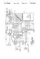
- FIG. 1is a simplified schematic representation of an exemplary kinetic measurement system 10 embodying the present invention.
- the system 10includes a light assembly 12 capable of providing a finely focused reflected beam of light for coupling to the test or assay sites.
- the light assembly 12comprises a single source of uniform, reflected and focused light 14 which, in the preferred embodiment, includes a tungsten-quartz bulb emitting light in a wavelength range of about 300 to 900 nanometers.
- the output of the light source 14is passed through a chopper 16 which modulates the light at a fixed frequency which in the preferred embodiment is 800 hertz.
- the modulated light from the chopper 16is collimated through a lens 18 onto a filter wheel 19 which extracts light of a selected wavelength and bandwidth which corresponds to the wavelength at which the test samples exhibit light absorbency.
- the filtered lightis passed through a lens 20 which receives the collimated light and focuses it onto a precise point 22 from which the light can be coupled to selected fibers which conduct the light to the plurality of assay sites.
- the kinetic measurement system 10utilizes a highly efficient and structurally simple light coupling and transmitting mechanism.
- the collimated light exiting the light assembly 12is directed to a light coupling arrangement which includes a cylindrical rotor 24 which is capable of being rotatably positioned accurately about its axis.
- the rotor 24includes an optical fiber 26 having an input end 28 located at the center of the rotor 24 and coincident with the focal point 22 of the light output from the light assembly 12.
- the output end 30 of the fiber 26is located near the periphery of the fiber rotor 24 so that as the rotor rotates the input end 28 of the fiber remains stationary with respect to the light assembly 12 while the output end 30 moves around a circular path.
- the rotor 24thus permits efficient coupling of light from the light assembly 12 into selected ones of a plurality of light transmitting means which carry the light to corresponding assay sites.
- the light output from the fiber 26 in the rotor 24is received by a fiber optic distributor 32 containing a multiplicity of optical fibers 34 having their input ends arranged in a circular array.
- This circular array of fiber endshas the same radius as the location of the output end of the fiber 26 in the rotor 24 so that as the rotor 24 is indexed about its axis, the output end of the fiber 26 is brought into alignment with successive fibers 34 in the distributor 32.
- the fibers 34are brought together to form a fiber bundle 36 which leads to a fiber manifold 38 which aligns each of the fibers 34 with one of the assay sites (to be described below).
- the rotor 24is indexed by means of a suitable stepper drive or other appropriate controllable displacement means so that it sequentially directs the collimated light from the focal point 22 into different fibers 34 of the bundle 36.
- optical fiber coupling arrangementto couple light from the light assembly 12 to individual optical fibers 34 within the distributor 32 constitutes a significant advantage because of the efficiency of transmission associated with the mechanism. More specifically, the optical fiber 26 ensures that substantially all the collimated light from the light source 14 is coupled into a selected optical fiber 34 without any significant diffusion at the point of coupling at either end of the coupling fiber 26. Thus, light from the source 14 is coupled through the rotor 24 only into a selected one of the optical fibers 34 with minimal undesired coupling of light into optical fibers adjacent to the selected fiber. This highly efficient coupling allows the use of a single light source with relatively low power capacity since a high percentage of light emanating from the source is transmitted to the site of measurement.
- the illustrated light source in FIG. 1is a convenient and preferred form; however any light source or a plurality of light sources providing light of equal intensity and having the desired range of wavelength can be used.
- an alternative form of photometric measurementwhich is based upon a sequentially operated multibeam light source, will be described in detail below in connection with FIGS. 8-13.
- sample plate 40may be a conventional microplate having a series of wells, usually an array of 96 wells arranged in 8 rows having 12 wells each.
- the sample plateis preferably mounted in an area where the ambient temperature is regulated, e.g., by means of a fan, so as to present isothermal conditions about the sample plate. This is important in minimizing inaccuracies from varying rates of reaction occurring at different sample sites as a result of a temperature gradient about the sample plate.
- An array of photodetectors 44is provided on a detector board 46 in the form of a matrix conforming to the positions of the wells located on the sample plate 40.
- a second lens array 48is positioned beneath the sample tray 40 and serves as means for focusing light from each well of the sample plate 40, after the light has passed through the well.
- the lens arrays 42 and 48are of the conventional type and include apertures (not shown) which function to direct the light towards the individual lenses and minimize diffusion of light into adjoining lenses.
- the sample plate 40is translucent or transparent so that light coupled to a particular optical fiber within the fiber manifold 38 and then collimated onto a corresponding sample well penetrates the well and its contents, passes through the corresponding focusing lens disposed within the lens array 48, and reaches the corresponding photocell 44 located immediately below the sample well.
- the photodetector 44senses the intensity of the light passing through the corresponding sample well and produces an electrical output signal proportional to the intensity of light incident on its surface.
- Each of the photodetectors 44 provided on the detector board 46functions in a similar manner and provides a signal which is proportional to the varying intensity of the light impinging thereon. This varying intensity is caused by the varying transmittance offered by the sample as a chemical reaction progresses therein and alters its constituency.
- the resulting electrical signals from the photodetectors 44are fed to an analysis and indication system 50 which processes the received signals and provides an external indication of the transmittance or optical density of each of the samples contained within the multiple wells of the sample plate 40.
- the measurement system of FIG. 1also includes a single reference optical fiber 52 positioned adjacent to the focal point 22 so that the fiber 52 receives light continuously whenever the light source 14 is energized, i.e., whenever any of the sample sites is being tested.
- the light emanating from the output end of the reference fiber 52is coupled through air or an empty sample well to a separate photodetector 45 on the detector board 46, and provides a reference photodetector signal whose significance will be described in detail below.
- the optic fiber distributor 32also has an optical fiber designated as the "home" fiber which serves as a reference for determining the current position of the distributor 32 relative to the coupling rotor 24.
- the function of the home fiberwill also be described in more detail below.
- the measurement system of FIG. 1is provided with means for agitating the chemical solutions contained within the plurality of wells of the sample plate 40. More specifically, as shown in FIG. 1, the sample plate 40 is attached to an agitating mechanism 54 which oscillates the tray in a manner that brings about a thorough mixing of the chemical solutions contained within the sample wells.
- the sample plate 40is connected to an agitation mechanism 54 which comprises a motorized arrangement capable of imparting gentle oscillatory motion to the sample plate at a desired frequency of oscillation.
- the agitation mechanism 54oscillates the sample plate with the same reversible drive motor generally used to control the position of the sample plate, by energizing the motor repeatedly in opposite directions at the desired rate of oscillation. Satisfactory results are obtained by oscillating the sample plate over a distance of about 1/16th of an inch at a frequency of about 20 Hz.
- the measurement systemis programmed to oscillate the sample plate before each reading.
- the oscillationis followed by a short time delay before the start of the reading phase to allow the reacting solutions within the sample wells to settle.
- the delay intervalprevents erroneous readings due to reflection and/or refraction effects arising from ripples caused by the agitation process.
- Typical time periodsare 3 seconds for the agitation phase and 1 second for the delay interval.
- the agitationneed not be effected by mechanical means, as long as the objective of achieving homogeneous color distribution effect is realized.
- Other suitable agitation meanssuch as "ultrasonic" vibration inducement, may be used, depending upon the desired efficiency and the constituency of the reacting agents.
- the oscillatory movement of the sample plateneed not be limited to lateral or rotational movements parallel to the plane of the sample plate; vertical oscillation (up-and-down movement) can also be used satisfactorily as long as spilling of test samples can be avoided.
- the fiber manifold 38is shown in more detail, including the disposition of the various optical fibers across the lower surface of the manifold. It will be noted that this particular embodiment of this invention is designed for the sequential assaying of samples contained in a conventional microplate which has 96 test sites or wells arranged in 12 ⁇ 8 matrix. Accordingly, as shown in FIG. 2, the fiber manifold 38 has 96 fibers arranged in 8 rows A, B, C, D, E, F, G and H, each row consisting of 12 fibers. For instance, the row A has 12 fiber ends A 1 , A 2 , A 3 . . . A 12 .
- the arrangement of the 12 rows A-H and the separation between adjacent fiberscorresponds exactly to the arrangement of the sample test sites in the sample plate used for the assay.
- light transmitted through a particular fiberis collimated directly onto the corresponding sample well and passes through to the corresponding photodetector, thereby generating an electrical signal having a magnitude proportional to the intensity of the light impinging on the photodetector.
- FIG. 3is a schematic representation of the fiber distributor arrangement showing the circular array of the input ends of the various fibers located in the fiber manifold 38.
- the distributor 32carries the input ends of each of the 98 optical fibers disposed within the fiber manifold. These 98 fibers are arranged in a circular array around the distributor 32.
- the input end of the "home” fiberis located in a position preceding the first row A of optical fibers.
- Three opaque spotsare located between the "home" fiber and the first fiber A 1 which corresponds to the first sample site to be assayed; these opaque spots serve to reference the start of a new assay sequence, as will be described below.
- FIG. 4there is shown a block diagram of the processing circuitry used for the analysis of the signals generated by the photodetectors 44.
- the detector board 46actually has 98 photodetectors 44, 96 of which correspond to the 96 sample sites of the sample plate 40 (FIG. 1), one of which receives light focused upon it from the reference fiber 52, and one of which receives light from the "home" reference fiber. It will be apparent that only a single reference photodetector is required if a single fiber is used to perform both the light and home reference functions.
- the signals generated by the 96 photodetectors for the sample sitesare converted to a corresponding voltage form by a current-to-voltage converter 110. These signals are then passed through a band limiting low pass filter 111 and subsequently to a multiplexer 112 which functions to controllably select desired ones of the 96 signals for further analysis according to a pre-programmed sequence.
- the signals generated in response to light from the light reference fiber 52 and the "home" fiberare converted into their equivalent voltage form by current-to-voltage conversion units 113 and 114 and then passed through band limiting low pass filters 115 and 116, respectively.
- the outputs of the multiplexer 112 and the two low pass filters 115 and 116are fed to a second multiplexer 118 which functions to controllably select one of the three signals at its input for further analysis.
- the "home” reference fiberprovides a convenient means for locating the angular position of the fiber 26 in the rotor 24 relative to the fiber distributor 32. More specifically, the "home” reference fiber serves as a means for ensuring that the rotor 24 is positioned correctly so that the light output from the coupling fiber 26 is directed to the proper optical fiber in the distributor 32 to begin a sequential assaying process. Since any light entering the "home” reference fiber is transmitted directly to a dedicated “home” photodetector 44, the existence of a peak signal at the output of the "home” photodetector is an indication that the rotor 24 is positioned at a so-called “home” position where the coupling fiber 26 is aligned with the "home” reference fiber.
- the measurement systemfirst positions the rotor 24 at its "home” position. In order to accomplish this, the rotor 24 is rotated while monitoring the output of the "home” photodetector, until a peak output signal from that photodetector is detected. Since the position of the "home" reference fiber relative to the first optical fiber A 1 is a known factor (in this case, separated by the three opaque spots), subsequent alignment of the coupling fiber 26 with the fiber A 1 can be conveniently accomplished by stepping the rotor 24 through three consecutive positions.
- the provision of the light reference fiber 52serves as a calibration means by which only the differences in sensed light intensity from one reading to another may be utilized for analysis of sample transmittance, thereby eliminating the effects of variations in the light output of the light source, system drifts and the like. More specifically, each time an assay is performed, the signal produced by the light reference fiber is measured before the start of the reading cycle. Then all subsequent signals produced by the photodetectors for the test sites are scaled relative to the signal initially produced by the light reference fiber. In this way, only actual changes in the transmittance of the liquid samples as a result of the chemical reactions occurring at the sample site are measured. Any localized differences in intensity such as those resulting from fluctuations in light intensity from the light source over the course of its lifetime, or premature readings taken before the light source or other system parameters have had a chance to stabilize, are disregarded.
- the "home" reference fiberis coupled directly to the corresponding photodetector, it can also be conveniently used as a reference light reading source and can effectively provide all functions performed by the light reference fiber as described earlier, in addition to providing a reference for determining the position of the fiber rotor 24 relative to the fiber distributor 32.
- the signal selected by the multiplexer 118is passed through a conventional bandpass filter 119 with a reasonably large bandwidth centered about the frequency at which the chopper 16 modulates the light passing through it (e.g., 800 hertz).
- the bandwidth of the bandpass filter 119is selected to be sufficiently large to accommodate the fluctuation in signal settling time that occurs as a result of rapid readings being performed on the sample plate.
- the band-limited output of the filter 119is then fed to a variable gain amplifier 120 whose function will be described below.
- the output of the amplifier 120is fed to a two-way switch 122 which in its normally closed position provides a direct electrical connection from the amplifier 120 to the subsequent portion of the processing circuitry.
- the switch 122serves as a virtual short circuit for measuring the signal generated only by the rest of the processing circuitry.
- the switch 122serves as a means for determining the "dark current" flowing through the processing circuitry in the absence of any light passing through the fiber distributor 32. This dark current measurement is free from distortions and noise from sources preceding the two-way switch 122, because the section of the processing circuitry in which the current is measured is totally isolated from the rest of the measurement circuitry. The significance of taking such readings while the circuit is isolated from the light source will be described below.
- the output signalis passed through a high pass filter 124 which in combination with the low pass filters 111, 115 and 116 provides secondary bandpass characteristics to the processing circuitry.
- the output of the high pass filter 124is fed through a phase detector 126 which in conjunction with a reference input from the light source chopper 16 and a low pass filter 128 functions to extract a direct current signal corresponding to the alternating current resulting from the modulating effect of the chopper 16. More specifically, the phase detector 126 effectively inverts the negative portions of the alternating output signals from the detector board 46 on the basis of the timing input provided from the chopper 16. The average value of the resulting signal represents the DC equivalent of the alternating signal. To extract this average value, the output of the phase detector 126 is fed through a low pass filter 128.
- the output signal from the low pass filter 128is fed to a second variable gain amplifier 130 which is a high precision amplifier providing a series of well defined gain settings.
- the operation of the variable gain amplifier 130 in conjunction with the first variable gain amplifier 120 in providing controllable accuracy and increased dynamic range for the processing circuitry of this inventionwill be described in detail below.
- the output of the amplifier 130is passed through a low pass filter 132 and then on to an analog-to-digital converter 134 which functions to translate the amplified analog signal into its corresponding digital form.
- the digital signals produced by the analog-to-digital converter 134are then fed to a conventional digital microprocessor system which performs a series of mathematical calculations and comparisons required to determine the optical density of the samples on the basis of a predefined algorithm.
- the same digital microprocessor systemis also used to regulate the sequential scanning of the plurality of test sites, the different multiplexing arrangements, and all related processing circuit functions.
- the measurement systemis made more efficient and economical by effectively augmenting the dynamic range of the analog-to-digital converter used to represent the analog signals defining the processed values of the various signals produced by the photodetectors.
- the variable gain amplifiers 120 and 130function to adjust the extent to which the processed signals are amplified in such a way that even when the signals vary over a wide range of amplitudes, a major portion of the quantization levels of the analog-to-digital converter is utilized without exceeding its original dynamic range.
- the actual operation of the amplifierswill be clarified by considering the case where the ADC 134 in FIG. 1 having a 12-bit capacity so that the total number of quantized output levels is 4096, ranging from 0-4095.
- the intensity of the resulting lightalso varies. This, in combination with variations in light transmission characteristics from one optical fiber to another and the frequency response characteristics of the photodetectors themselves, as well as changes in transmittance due to chemical changes in the samples, can produce signals whose amplitudes vary over a significant range.
- variable gain amplifiers 120 and 130initially process the incoming signal at very low gain settings.
- the resulting digital outputis then compared with the maximum possible value of the ADC output in order to determine the maximum possible gain to which the incoming signal may be subjected without exceeding the maximum digital output value of the ADC. For instance, if an input signal produces an ADC output of about 50 counts at the initial gain setting (which are normally 1), the system compares this count value to the maximum count value possible with the ADC which, in the case of the 12-bit ADC, is 4095 and determines the extent to which the signal may be safely amplified so that the digital output falls within the maximum count value.
- a safety margin of about 10%is built into this dynamic ranging process by performing the above comparison not on the basis of the maximum output value of the ADC but instead by comparison with a value that is roughly 90% of the maximum output.
- the actual count of 50would hence be divided into a safety-adjusted maximum output of 3686 counts to give a desired amplification factor of about 74.
- the gain settings of the variable gain amplifiersare adjusted to closely approximate the desired gain factor.
- the gain G1 of the first variable gain amplifier 120is adjusted on the basis of the signal derived from light being transmitted through air, whereas the gain G2 of second variable gain amplifier 130 is adjusted on the basis of the signals derived from the sample site photodetectors.
- FIG. 5is a flow diagram of the general sequence of operations involved in a typical sequential scan according to the system of this invention.
- the sequencebegins at step 150 where the various system variables, such as the number of readings to be made within the kinetic reading cycle, duration of agitation, the duration of the delay following the agitation phase, etc., are initialized.
- the air calibration phaseis carried out by performing a reading upon each of the sample wells through air. Measurements made during the air calibration phase are performed with a unity gain setting G2 for the second variable gain amplifier 130 and the gain G1 of the first variable gain amplifier 120 is optimized for the maximum dynamic range of the analog-to-digital converter.
- G2unity gain setting
- G1 of the first variable gain amplifier 120is optimized for the maximum dynamic range of the analog-to-digital converter.
- the air calibration phase 152is followed by step 154 where a kinetic reading cycle is initiated upon the basis of the initialization data provided to the measurement system as part of step 150.
- the kinetic reading cycleincludes the execution of the agitating, delay and reading steps at each of a series of pre-programmed discrete time intervals at which optical density readings are to be taken for the particular samples being measured. It will be apparent that, in the case of end-point analysis, the reading cycle will comprise the execution of the above steps only at a single time interval.
- Step 156is the read phase, which includes a series of three steps beginning with the agitation phase 158 during which the sample plate is vibrated for a pre-defined time interval. Subsequently, at step 160, the settling phase takes place during a pre-defined delay interval in which the oscillation mechanism is dormant and the reaction agents within all the sample wells of the sample are allowed to settle down for a pre-defined time interval before obtaining the actual signal readings.
- the measurement systemobtains the transmittance reading on all the wells of the sample plate. This step includes optimization of the gain setting G2 for the second variable gain amplifier 130 while maintaining the gain setting G1 of the first variable gain amplifier 120 at the optimized value determined during air reference. The sequence of events involved in the read step 162 will be described in detail below.
- step 164determines whether the system has completed the pre-defined kinetic reading cycle. If the answer at step 164 is no, step 166 continues the kinetic reading cycle.
- the read phase 156is reiterated by the measurement system until the agitation phase and the accompanying delay and read sequences have been performed at each of the prescribed intervals of the kinetic reading cycle. If it is found at step 164 that readings have indeed been performed at all prescribed time intervals, the measurement system comes to a stop. This marks the end of the kinetic reading cycle.
- the reading cyclehas been described above only with respect to the sequence of operations undergone by the illustrative photometric measurement divide in obtaining the various light readings required to calculate the optical density at the sample sites. It will be understood that the microprocessor system which forms part of the analysis and indication system (FIG. 1) processes the data resulting from the measurements as the reading cycle proceeds and initiates computation of optical density values (on the basis of a pre-defined algorithm as will be explained below) for those sample sites and time intervals for which required measurements have been completed.
- OD nThe calculated optical density of a given sample well (where n varies from 1 through 96 in order to designate each of the 12 sample wells positioned along each of the 8 rows A through H of the microplate).
- W nThe signal output of a photodetector corresponding to a given sample well containing the reacting sample.
- G1The adjustable gain of the first stage variable gain amplifier 120 (controllable by a set of gain multiplication factors including 1, 2, 4, 8, 16, 32, 64 and 128).
- G2The adjustable gain factor for the second stage variable gain amplifier 130 (adjustable by a set of gain multiplication factors including 1, 10 and 100).
- D nThe dark current reading taken with the two-way switch 122 of FIG. 4 in its open position, for a given sample well. This reading is taken with the first stage gain setting G1 set to 1 and at the same second stage gain setting G2 used to obtain the corresponding W n signal output.
- D readThe dark current readings taken at the beginning of a READ cycle.
- the measurement systempositions the rotor 24 at the reference "home” position by sequentially displacing the rotor until the existence of a peak signal is detected at the output of the "home" reference photodetector.
- the gain settings for both the first and second stage variable gain amplifiers 120 and 130are set to unity.
- step 202the measurement system switches to either the photodetector for the light reference fiber or the photodetector for the home reference fiber in order to measure the light reference signal L.REF air .
- This readingis measured with the gain G2 of the secondary stage variable gain amplifier set to unity and the gain G1 of the first stage variable gain amplifier optimized to provide the largest count value at the output of the analog-to-digital converter 134 (according to the safety-adjusted dynamic ranging procedure described above).
- the measured reference signal value L.REF air and the optimized first stage gain setting G1 L .airare stored in the memory of the microprocessor system for later use in the optical density calculations.
- the rotoris displaced through a designated number of positions relative to the "home" position so as to locate the rotor at a position corresponding to one of the three opaque spots X 1 , X 2 and X 3 on the fiber distributor 32.
- the rotoris actually displaced by two positions relative to its home position so that the coupler comes to rest at a position corresponding to the opaque spot X 2 .
- the opaque spoteffectively blocks the coupling of any light from the coupling fiber 26 into any of the fibers in within the fiber manifold 32 and hence isolates the light source from the photodetectors.
- the dual position dark current switch 122activated and a dark current reading D air is taken with both the first and second stage gains G1 and G2 set to unity.
- the dark current reading D airrepresents the residual current flowing within the portion of the processing circuitry of FIG. 4 following the two-way switch 122. This value is subtracted from the signal reading of every sample well in order to provide a true representation of the transmittance value for the sample well at any designated time.
- the measured dark current reading D airis stored in the system memory for later use in calculating the optical density.
- the measurement systemis ready to perform air calibration readings on each of the sample wells. Accordingly, at step 208, the rotor 24 is advanced to the position A 1 corresponding to the first sample well of the microliter plate, and the photodetector corresponding to the sample well A 1 is switched on.
- the air calibration signal reading W.AIR n for the sample well A 1is taken with the gain G2 of the secondary stage variable gain amplifier set to unity and the gain G1 of the first stage variable gain amplifier optimized to a value G1 A1 ; the latter value represents the gain setting which allows the maximum safety-adjusted output from the analog-to-digital converter without exceeding its rated dynamic range.
- step 212the microprocessor system checks to determine whether air calibration has been performed at each of the 96 sample well sites on the sample microplate. If the answer at step 212 is negative, step 214 advances the rotor to a position corresponding to the succeeding sample well site before reverting to the air calibration step 210. If the answer at step 212 is positive, i.e., air calibration has indeed been performed on all 96 sample well sites, it marks the end of the air calibration sequence at step 216. It will be noted that the entire air calibration sequence is performed with the sample plate in its retracted position, i.e., away from the photodetector board so that light from the fiber manifold 38 is transmitted directly to the photodetectors.
- FIG. 7there is shown a flow chart of the sequence of operations undergone by the measurement system while performing the read phase. It should be noted that before actual reading is performed on a a sample plate, the measurement system proceeds through the air calibration phase with the sample plate in its retracted position. Prior to the start of a read phase, the sample plate is moved into its advanced position in preparation for the reading phase.
- the measurement systemlocates the rotor at the "home" position.
- the signal from the "home" reference fiber photodetectoris tracked by the processing circuitry with both the first and second stage variable gain amplifiers having their gains G1 and G2 set to unity.
- Step 302is then accessed, where a measurement of a light reference signal occurs. More specifically, the measurement system switches to the photodetector corresponding to the light reference fiber (or the photodetector corresponding to the home reference fiber if this fiber is being used to perform the functions of the light reference fiber), and a light reference signal L.REF read is taken with G2 set to unity and G1 optimized to its maximum value Gl L .air according to the dynamic ranging procedure described above. Also as part of step 302, the measured L.REF read value is stored in the system memory for later use during calculations of optical density.
- the rotor 24is displaced through a designated number of positions to locate it at one of the three opaque spots X 1 , X 2 and X 3 provided on the fiber distributor 32. More specifically, the rotor is stepped two positions relative to the home reference fiber so as to be located at the second opaque spot X 2 .
- step 306actuates the dual position switch 122 and measures a series of dark current readings D air .X with the first stage variable gain G1 set to unity. A single reading is taken at each of the possible gain settings G2 (in this case 1, 10 and 100) of the secondary stage variable gain amplifier. The measured values of D air .X are also stored within the system memory as part of step 306.
- the rotoris advanced to the first sample well position A 1 .
- the systemswitches to the photodetector corresponding to the first sample well A 1 to begin the actual sequential reading cycle.
- the succeeding step 310activates the agitation mechanism for a predesignated time interval T 1 to promote homogeneous color distribution as described above.
- the agitation phase of step 310is succeeded by a settling phase at step 312 during which the agitation mechanism is deactivated and the system dwells for a time interval T 2 to allow the agitated samples to settle down in preparation for performing transmittance readings upon them.
- the agitation phase at step 310may entail displacement of the sample from its position between the fiber manifold and the photodetector board to permit oscillatory movement of the plate. Accordingly, the settling phase may actually take place during the time it takes to reposition the plate from its agitation position to its reading position. Immediately after agitation and the subsequent settling of the reacting samples within the sample plate, optical density readings are taken.
- the signal W An for the first sample welli.e., A 1
- G 1set to the corresponding stored gain value G1 A1 determined as part of the air calibration (step 210 in FIG. 6).
- G2is initially set to unity and then optimized to a value that produces the maximum safety-adjusted output value from the analogto-digital converter of FIG. 2.
- the measured signal value W A1is stored within the system memory for use in calculation of the optical density for that sample well.
- the microprocessor systemperforms a check to determine whether signal readings have been obtained for all 96 sample wells. If the answer at step 316 is negative, the microprocessor system advances the rotor to a position corresponding to the next sample well. At the same time, the processing circuitry switches to monitor the photodetector corresponding to the selected sample well. The system then reverts to step 310 and goes through the agitation, settling and read steps 310, 312 and 314 again. These three steps are reiterated until the check at step 316 produces a positive answer, indicating that signal readings have been obtained from all sample wells. This marks the end the reading cycle at step 322.
- the gain G1 n for the first stage variable gain amplifier 120is individually determined for each sample well during the air calibration phase, and then is maintained constant for all subsequent readings in that kinetic reading cycle. The value of G1 is not adjusted again until the next air calibration phase.
- the gain G2 n for the second stage variable gain amplifieris set equal to unity for all air reference and light reference readings, so that the dynamic range of the second stage amplifier 130 is utilized only when actual transmittance readings are being taken, and not for air reference readings.
- the first quantity (W.AIR n -D air )/(W n -D n )is the ratio of the adjusted signal readings for a given sample well (1) without any sample and (2) with a sample. All readings measured by the processing circuitry of the microprocessor system are adjusted for any offset voltages generated by the analog-to-digital converter or other system offsets and drifts by taking into account the corresponding dark current readings, as indicated in the above equation for OD n . For instance, the signal reading W.AIR n is normalized for dark current effect by subtracting from it the value D air of the corresponding dark current reading. Similarly, this signal reading W n is adjusted by subtracting from it the corresponding dark current reading D n .
- the second quantity (L.REF read -D read )/(L.REF air -D air )is a measure of the ratio of the light reference readings obtained for a given sample well during the air calibration phase and the read phase. These two readings are also normalized on the basis of the corresponding dark current readings.
- the third quantity (G2 n ) in the above equationaccounts for the effect of the dynamic ranging procedure described above, i.e., this quantity neutralizes the effects of amplification of the signal readings by the processing circuitry.
- the computation of the logarithms required to calculate the optical density readingsis performed by storing all the required logarithmic values within the microprocessor system in the form of a look-up table and subsequently using the digitized output of the processing circuitry as an index to retrieve the appropriate logarithmic value.
- the output signals of the photodetectors of the detector boardhave been fed to a logarithmic amplifier to obtain the logarithmic values of the output signals.
- This techniqueis subject to a variety of problems and limitations because of the constant need to adjust the system for offset gains of the logarithmic amplifiers.
- any temperature drift in the computing hardwaremust be accurately tracked and appropriately compensated to retain the accuracy of computation.
- the computation of the logarithmic valuesis made substantially more accurate and independent of the system hardware parameters by storing within the microprocessor system memory all possible logarithmic values that would be required by the system in order to compute the optical density readings.
- the look-up tablecontains logarithmic values corresponding to each of the possible output quantization levels for the analog-to-digital converter of the system (as shown in FIG. 4).
- the possible quantization levelsrange from 0 to 4095. This means that there are 4096 different values that a signal may take after it has been detected, processed and digitized.
- the logarithmic value corresponding to each of these 4096 possible valuesare stored within a logarithmic look-up table which is contained within the ROM portion of the microprocessor system.
- the logarithmic look-up tableis defined in such a way that the digitized output from the analog-to-digital converter serves as an address or index that points to the corresponding logarithmic value stored within the look-up table.
- the process of selecting a particular photodetector from the multiplicity of detectors on the detector boardis simplified by use of a tiered parallel addressing scheme for the photodetectors. More specifically, the photodetectors are divided into a selected number of blocks, each block consisting of a plurality of photodetectors. Corresponding photodetectors in the various blocks are connected in a parallel fashion in such a way that if, for instance, the first photodetector in the first block is addressed, the measurement system also automatically addresses the first photodetectors in the remaining blocks.
- the detector boardcomprises 97 photodetectors (96 for the 96 sample wells and 1 for the "home" and light reference fiber).
- the 96 sample-well photodetectorsare divided into blocks consisting of 16 photodetectors each.
- the first blockconsists of the photodetectors A 1 --A 4 , B 1 -B 4 , C 1 -C 4 and D 1 -D 4
- the second blockconsists of the photodetectors A 5 -A 8 , B 5 -B 8 , C 5 -C 8 and D 5 -D 8
- the third blockconsists of the photodetectors A 9 -A 12 , B 9 -B 12 , C 9 -C 12 and D 9 -D 12
- fourth blockconsists of the photodetectors E 1 -E 4 , F 1 -F 4 , G 1 -G 4 and H 1 -H 4
- the fifth blockconsists of the photodetectors E 5 -E 8 , F 5 -F 8 , G 5 -G 8 and H 5 -H 8
- the sixth blockconsists of the photodetectors E 9 -E 12 , F 9 -F 12 , G 9 -G 12 and H 9 -H 12 .
- the first photodetectors in all of the blocksthat is A 1 , A 5 , A 9 , E 1 , E 5 and E 9 , are connected in parallel, and the rest of the photodetectors are connected in a similar fashion.
- FIGS. 8-13relates to a preferred embodiment of a rapid solid state multibeam photometer for multi-site microanalysis which can perform a large number of readings in a short period of time without requiring mechanical movement of the optical components or the microplate or other multi-site assay sample.
- a number of light sourcesare arranged so that one light source shines on each of the assay wells or spots.
- At least one monolithic photodetectoris employed such that light coming from a plurality of different assay sites can be detected at a plurality of different sites on the surface of the photodetector.
- the light sourcesare turned on in sequence so that only a single light source is shining at any one time.
- the signal detected by the photodetectorwill correspond to the particular well or spot in the sample beneath the light source which is turned on at that time.
- an array of 96 light-emitting diodesis arranged above the 96 wells of a microplate or sample spots on microplate format filter.
- At least one silicon photodetectoris arranged beneath the microplate or filter with an area corresponding to the area of a plurality of the wells on a microplate.
- Solder connecting lines to the top layer of the photodetectorare arranged in a criss-cross fashion to correspond to the area between the sample sites so that light is not blocked.
- the use of the large photodetectorresults in a large noise problem.
- This noiseis overcome by a number of features.
- the primary noise signal encounteredis the 60 Hz line power signal.
- the effect of this noise signalis counteracted by taking 10 readings for each well, with each reading being synchronized to occur 36° after the previous reading in 60 Hz phase space. For 10 readings, the time between readings equals: ##EQU2## where n is an integer.
- 60 Hz noise encountered on one readingshould be cancelled out by noise encountered on another reading at an opposite phase when the 10 samples are averaged.
- Noiseis also reduced by the use of high-frequency sequencing of the LED's rather than having the light source constantly on.
- a filteris then used to eliminate noise which occurs at frequencies above the LED sequencing frequencies. Measurements are made at this high frequency for both an on and an off state for each LED. The off state measurement will give a reference level corresponding to the noise in the system at frequencies below that of the sequencing frequency. Because the off state measurement is done immediately after the on state measurement, the noise level should be approximately the same in both states and cancel out.
- a disadvantage with using LED's and a large photodetectoris that both have characteristics which drift with temperature. These characteristics can change in just a few minutes. Devices which utilize a tungsten light source and small photodiodes do not have drift problems of the same magnitude. This drift problem is overcome by the following steps. A reading is first taken without the sample being inserted to give a photosignal value corresponding to the light transmission through the airspace between th LED's and the photodetector. A second reading is then taken immediately thereafter of a microplate filled with water (blank plate), buffer or any other base solution in which the chemical reactions are to take place or of a blank filter. This will give a "blank" photosignal level reading corresponding to the light transmission through the blank plate.
- FIG. 8there is shown a perspective view of a presently preferred embodiment of a multibeam photometer according to the present invention.
- a photometer 2is depicted comprising circuit board 4, the details of which will be described below, monolithic photodetector 6, LED array 8, and drawer-type sample holder 10.
- a microplate or sample tray 14is usually placed in opaque mask 16 adapted to isolate the sample tray well walls while allowing light to pass through each sample well from top to bottom or vice versa. This assembly is then placed in open receptacle 18 of sample holder 10. The reader is activated by returning sample holder 10 to the closed position which activates a microswitch, indicating that the sample may be read.
- FIG. 9is a side elevation cutaway view of a microplate well inserted into mask 16 and placed between photodetector 6 and LED array 8.
- microplate format filtersmay be read by placing the filter in a holder adapted to isolate each sample site one from another while permitting light to pass through each individual sample site.
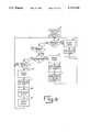
- FIG. 10shows a block diagram of the electronic control circuitry according to the present invention.
- a central processing unit (CPU) 40controls the operation of the circuit and for each LED to be illuminated sends a data signal on data bus 42 to decoders 44 and 46.
- the decoded signalsare sent through appropriate lines of busses 48 and 52 to a current driver array 50 and a current sink array 54, respectively, and through drive bus 56 and sink bus 60 to activate a particular LED in LED array 8.
- Lightpasses through sample 14 to photodetector 6.
- the signal from photodetector 6passes through current-to-voltage converter 66, sample and hold circuit 68, analog-to-digital A/D converter 70, through data bus 72 and back to CPU 40 for analysis.
- CPU 40can be a standard CPU board having a microprocessor, random access memory (RAM) and read only memory (ROM), such as the Microsystems 5323.
- RAMrandom access memory
- ROMread only memory
- Decoder 44decodes a portion of the data designating the correct column of the LED to be illuminated, and activates the appropriate line of data bus 48 to current driver array 50.
- Decoder 46decodes the portion of the data corresponding to the appropriate row of the LED to be illuminated and activates a data line of data bus 52 connected to current sink array 54. Current is then passed through the appropriate line of current driver bus 56, through the appropriate diode of 8 ⁇ 12 LED array 8 and then through an activated line of sink bus 60 to the corresponding current sink in current sink array 54.
- the light from a particular LED in LED array 8will pass through a well in sample tray 14 and be detected by photodetector 6.
- the current generated in photodetector 6will be converted into a voltage level by current-to-voltage converter 66.
- a sample and hold circuit 68will sample this analog voltage level at a period in time controlled by CPU 40.
- This analog valuewill be converted into a digital value by A/D converter 70.
- the digital datais passed along data bus 72 to CPU 40. Data from CPU 40 can be passed along to a printer 74.
- CPU 40is controlled by an operating program which decides when data is to be analyzed, printed or sent to decoders 44 or 46 to illuminate an LED.
- a software clock on a line 76indicates when an LED is to be illuminated. The timing of this software clock relative to a 60 Hz line noise signal may vary because of the variation in the number of program steps needed to complete an operation being performed when the program is interrupted to take a reading.
- software clock 76is gated with a hardware clock 78 in a gate 80. Accordingly, the absolute time of each LED illumination can be precisely controlled.
- the output of gate 80is coupled to a clock input of decoders 44 and 46.
- Photodetector 6is a rectangular silicon cell with N-doped material on the top and P-doped material on the bottom.
- the N-doped layeris thin enough to allow light to pass through.
- the natural reverse bias of the silicon cell due to the diffusion of holes and electronsis sufficient for purposes of the present invention and no reverse bias voltage is added.
- Current driver array 50is supplied with current by a constant current source 82.
- the amount of currentcan be set to correspond to the desired amount and intensity of light to be emitted by each LED.
- FIGS. 11A and 11Bshow the detailed circuitry of portions of the block diagram of FIG. 10.
- the circuitry of FIG. 11Bis preferably located on the same circuit card as the 8 ⁇ 12 LED array.
- the circuitry of FIG. 11Acan be located remotely from the LED array on a separate card.
- a current-to-voltage (I/V) converter 66is shown which is adapted for coupling to the photodetector 6 of FIG. 10.
- a resistor 84 and capacitor 86can be adjusted to provide high frequency filtering of the signal from photodetector 6.
- the output voltage signal of I/V converter 66is applied to a sample and hold circuit 68.
- the sampling and holding functions of sample and hold circuit 68are activated by a trigger input 86. This input originates from one of the data lines in bus 88 to CPU 40 of FIG. 10.
- Output 90 of sample and hold circuit 68is provided as an input to A/D converter 70.
- the maximum value which A/D converter 70 can acceptis 10 volts.
- Resistor 84 back in I/V converter 66can be adjusted so that the largest signals expected to be detected from the photodetector 6 will produce a voltage of just under 10 volts.
- the digital output of A/D converter 70appears on data bus 92.
- Data bus 92serves to provide the digital values from A/D converter 70 to CPU 40, as well as allowing the passage of data from CPU 40 to decoders 44 and 46.
- the tristate outputs of A/D converter 70will be directed to assume a high impedance state.
- the outputs of A/D converter 70are controlled by a chip enable signal 94.
- the digital output values from A/D converter 70consist of two 8-bit bytes. A digital signal on the byte address/short cycle input A 0 activates first the first byte and then the second byte on the outputs of A/D converter 70. Thus, more than one output of A/D converter 70 is shown coupled to each data line.
- a decoder 96provides an enable signal 98 to decoders 44 and 46 of FIG. 11B. This signal also serves as the software clock input to synchronizing circuit 80. The output of synchronizing circuit 80 is an inhibit signal 100.
- data signals D 0 -D 6are shown input to decoders 44 and 46.
- a constant current source 82provides current for current drivers 50 to LED array 58.
- the rows of LED array 8are coupled to current sinks 54, which are inverters having an open collector output.
- decoder 44When a particular LED is selected, a 7-bit digital code will appear on data lines D 0 -D 6 .
- decoder 44When an enable signal is provided and the inhibit signal is removed, decoder 44 will activate one output line and decoder 46 will activate one output line.
- the line activated by decoder 44will switch one of current drive transistors 50 which will provide current from current source 82 to all of the LED's in one of columns A-H.
- the output line activated by decoder 46will turn on one of inverters 54 to a low state output, thereby coupling the selected one of rows 1-12 to ground. This will allow current to flow through the selected one of the LED's in the selected one of rows A-H.
- a front panel display 12 in FIG. 11Ahas "ready,” “load,” and power on indicator lights as well as “set blank,” “read tray,” and “optical density (OD)/range” switches.
- the switches and lightsare controlled by signals from the CPU as discussed below.
- the operation of the circuit of FIGS. 10 and 11can be understood with reference to the timing diagram of FIG. 12.
- the sample and hold trigger signalis signal 86 of FIG. 11A
- the decoder inhibitis signal 100 of FIG. 11A and FIG. 11B
- the A/D chip enable signalis signal 94 of FIG. 11A.
- Two separate readingsare taken for each sample, one with the LED on and one with the LED off.
- the transmittance levelis the difference between the on and off readings.
- the sequences of the on and off readingsare shown separately. All 96 LED's are activated in sequence, and the process is repeated 10 times over equally spaced phase positions of a 60 Hz line noise signal.
- the sample and hold trigger signal on line 86produces a pulse every 250 microseconds (ms). This pulse pulse is generated in the CPU with the hardware clock from a crystal oscillator.
- the decoder inhibit signalis produced by a combination of the hardware clock and a software clock.
- the software clock signalis produced as soon after an interrupt signal in the CPU program as the operation of the CPU program can be interrupted . This amount of time can vary from 4 to 20 clock cycles, depending upon the status of program operation.
- a software clock signalis produced on line 98, it is combined with the hardware clock in synchronizing circuit 80 to produce a down going pulse on the decoder inhibit signal at time 104. This causes a particular LED to be turned on as explained before.
- Sample and hold circuit 68is enabled for sampling a value at time 106. This sample is locked in at a hold time 108. This hold time is delayed past the LED turn-on time 104 to allow the signal to be processed through current-to-voltage converter 66 and filtered through resistor 84 and capacitor 86.
- A/D converter 70has its tristate outputs enabled at a point of time 110 and data is read out in two bytes under the control of two chip enable pulses 112.
- a sequence for recording a sample when the LED is turned offbegins at a point of time 114 when the inhibit signal again appears, thereby disabling the decoders and removing current from the current drivers to turn off the LED's. Sample, hold, start of A/D and read of A/D signals follow accordingly.
- an experimental sample traycan be placed in the drawer.
- the plate readerwill again measure the airspace between the LED's and the photodetector immediately prior to reinsertion of drawer 10.
- the photosignal values as modified by the various wells of the sample trayare compared to values for the blank tray and are adjusted for variations in the airspace reading.
- a blank traycan be inserted initially and will not have to be reinserted for sample readings taken over the course of several hours or days.
- the adjustments for drift in the LED's and the photodetector with temperature over this time periodis made by the comparison of the two airspace readings immediately before the blank tray insertion and immediately before the particular sample tray insertion.
- the on-board software program which controls the operation of the microplate readeris shown in the flow chart of FIG. 13.
- the plate readeris first turned on and housekeeping functions are performed by the software (step A).
- the operatorthen pulls drawer 10 out.
- the "drawer out” stateis then detected (step B) and the LED's are scanned (step C) to produce a series of photosignal values (step D) corresponding to light transmission through the airspace. These values are put in a Table 3 in memory.
- step Ethe front panel switches are checked to see whether the drawer contains a blank tray (step F).
- step Fthe LED's are scanned (step G) and the photosignal values are put in a Table 1 in memory (step H).
- step HThe airspace values of Table 3 are then transferred to another Table 2 (step I) to provide a set of airspace readings close to the time of the blank plate reading producing the values of Table 1.
- the airspace readingsare done constantly when drawer 10 is out, thus constantly updating Table 3 prior to drawer 10 containing a tray being inserted.
- step JIf drawer 10 is inserted and the "set blank” switch is not thrown, the front panel switches are examined to determine whether the samples are to be red (step J). If the "read” switch has been thrown, the LED's are scanned (step K) and the transmittance values are put in Table 4 in memory (step L). The optical densities for the samples are then calculated (step M) and printed (step N).
- optical densityOD
- the optical density of the sample at site nequals OD n .
- each LEDis scanned starting with the first and proceeding through the 96th as discussed earlier. Ten repetitions are done equally spaced over the phases of a 60 Hz cycle.
- the final photosignal values used in the calculation described aboveare given by the sum of the 10 or minus off signals.
- the optical densityis the log of the blank value divided by the sample value adjusted for differences in the airspace readings.
- a photosignal reading in accordance with the flow chart of FIG. 13is initiated by an interrupt signal to a microprocessor in CPU 40.
- the program in the CPUcan cause data to be calculated or transferred to one of the tables or printed out on a printer.
- the actual reading itselfis sandwiched in between these other functions as dictated by the interrupt signal.
- the interrupt signalwill be interrupting a program operation, a certain amount of steps after the interrupt signal are necessary to basically hold the place in the program by moving data into memory or completing a step or otherwise.
- the amount of time between the initiation of an interrupt signal and the reading of an LEDcould vary (usually by between 4 and 20 clock cycles).
- the interruptis provided at least 20 clock cycles prior to when it is anticipated that a reading should be taken and is, in effect, ANDed with a real time clock in synchronizing gate 80 as shown in FIGS. 3 and 4. This ensures that the location of each reading relative to the phase of the 60 Hz noise signal will be precisely controlled.
- the operation of the plate readercan be controlled by another computer, such as a microcomputer coupled to the plate reader.
- a host computeroverrides the operation of the switches.
- the rapid solid state multibeam photometer as described aboveis characterized by its ability to reliably read transmittances of multi-site solid support assay samples in less than about 2 seconds without movement of the sample or holder. This is achieved by employing at least one monolithic photodetector of an area at least equal to the area of a plurality of multi-site solid support assay sites.
Landscapes
- Chemical & Material Sciences (AREA)
- Life Sciences & Earth Sciences (AREA)
- Health & Medical Sciences (AREA)
- Physics & Mathematics (AREA)
- Chemical Kinetics & Catalysis (AREA)
- Electrochemistry (AREA)
- Molecular Biology (AREA)
- Analytical Chemistry (AREA)
- Biochemistry (AREA)
- General Health & Medical Sciences (AREA)
- General Physics & Mathematics (AREA)
- Immunology (AREA)
- Pathology (AREA)
- Investigating Or Analysing Materials By Optical Means (AREA)
- Investigating Or Analysing Materials By The Use Of Chemical Reactions (AREA)
Abstract
Description
OD.sub.n =log(n.sub.1)(n.sub.3)/(n.sub.4)(n.sub.2).
Claims (1)
Priority Applications (1)
| Application Number | Priority Date | Filing Date | Title |
|---|---|---|---|
| US07/639,313US5112134A (en) | 1984-03-01 | 1991-01-08 | Single source multi-site photometric measurement system |
Applications Claiming Priority (3)
| Application Number | Priority Date | Filing Date | Title |
|---|---|---|---|
| US58533484A | 1984-03-01 | 1984-03-01 | |
| US42794289A | 1989-10-25 | 1989-10-25 | |
| US07/639,313US5112134A (en) | 1984-03-01 | 1991-01-08 | Single source multi-site photometric measurement system |
Related Parent Applications (1)
| Application Number | Title | Priority Date | Filing Date |
|---|---|---|---|
| US42794289AContinuation | 1984-03-01 | 1989-10-25 |
Publications (1)
| Publication Number | Publication Date |
|---|---|
| US5112134Atrue US5112134A (en) | 1992-05-12 |
Family
ID=27411570
Family Applications (1)
| Application Number | Title | Priority Date | Filing Date |
|---|---|---|---|
| US07/639,313Expired - LifetimeUS5112134A (en) | 1984-03-01 | 1991-01-08 | Single source multi-site photometric measurement system |
Country Status (1)
| Country | Link |
|---|---|
| US (1) | US5112134A (en) |
Cited By (81)
| Publication number | Priority date | Publication date | Assignee | Title |
|---|---|---|---|---|
| WO1994003791A1 (en)* | 1992-07-31 | 1994-02-17 | Molecular Devices Corporation | Metabolic monitoring of cells in a microplate reader |
| US5401465A (en)* | 1992-05-05 | 1995-03-28 | Chiron Corporation | Luminometer with reduced sample crosstalk |
| US5447692A (en)* | 1992-07-06 | 1995-09-05 | Beckman Instruments, Inc. | On-line process flow and reaction monitor |
| US5473437A (en)* | 1992-07-17 | 1995-12-05 | Becton Dickinson And Company | Methods and apparatus for detecting bacterial growth by spectrophotometric sampling of a fiber-optic array |
| WO1996005488A1 (en)* | 1994-08-08 | 1996-02-22 | Science Applications International Corporation | Automated system and method for simultaneously performing a plurality of signal-base assays |
| EP0677732A3 (en)* | 1994-04-15 | 1996-06-12 | Molecular Devices Corp | Photometric device. |
| EP0722136A3 (en)* | 1995-01-12 | 1996-08-28 | Schulz Joachim | |
| US5590052A (en)* | 1994-04-14 | 1996-12-31 | Abaxis, Inc. | Error checking in blood analyzer |
| US5589351A (en)* | 1994-12-06 | 1996-12-31 | Nps Pharmaceuticals, Inc. | Fluorescence detection apparatus |
| US5766875A (en)* | 1993-07-30 | 1998-06-16 | Molecular Devices Corporation | Metabolic monitoring of cells in a microplate reader |
| US5985214A (en)* | 1997-05-16 | 1999-11-16 | Aurora Biosciences Corporation | Systems and methods for rapidly identifying useful chemicals in liquid samples |
| US6043880A (en)* | 1997-09-15 | 2000-03-28 | Becton Dickinson And Company | Automated optical reader for nucleic acid assays |
| US6111636A (en)* | 1998-04-17 | 2000-08-29 | Labsystems Oy | Device for measuring optical density |
| US6159425A (en)* | 1997-07-16 | 2000-12-12 | Ljl Biosystems, Inc. | Sample transporter |
| WO2000065325A3 (en)* | 1999-04-27 | 2001-04-26 | Zeiss Carl Jena Gmbh | Array for optical evaluation of an object array |
| US6258326B1 (en) | 1997-09-20 | 2001-07-10 | Ljl Biosystems, Inc. | Sample holders with reference fiducials |
| US6297018B1 (en) | 1998-04-17 | 2001-10-02 | Ljl Biosystems, Inc. | Methods and apparatus for detecting nucleic acid polymorphisms |
| US6312901B2 (en) | 1996-07-08 | 2001-11-06 | Burstein Technologies, Inc. | Spatially addressable, cleavable reflective signal elements, assay device and method |
| US6331275B1 (en) | 1996-07-08 | 2001-12-18 | Burstein Technologies, Inc. | Spatially addressable, cleavable reflective signal elements, assay device and method |
| US6342349B1 (en) | 1996-07-08 | 2002-01-29 | Burstein Technologies, Inc. | Optical disk-based assay devices and methods |
| US20020071359A1 (en)* | 2000-12-08 | 2002-06-13 | Worthington Mark Oscar | Methods for detecting analytes using optical discs and optical disc readers |
| EP1223421A3 (en)* | 2001-01-10 | 2002-07-24 | Yokogawa Electric Corporation | Biochip reader |
| US20020098593A1 (en)* | 2000-11-17 | 2002-07-25 | Flir Systems Boston, Inc. | Apparatus and methods for infrared calorimetric measurements |
| US20020106661A1 (en)* | 1996-07-08 | 2002-08-08 | Burstein Laboratories, Inc. | Optical disk-based assay devices and methods |
| US20020118355A1 (en)* | 2000-11-08 | 2002-08-29 | Worthington Mark Oscar | Interactive system for analyzing biological samples and processing related information and the use thereof |
| US20020135754A1 (en)* | 1994-09-21 | 2002-09-26 | The University Court Of The University Of Glasgow | Apparatus and method for carrying out analysis of samples using radiation detector split beam radiation inspection |
| US20020146345A1 (en)* | 2000-11-17 | 2002-10-10 | Neilson Andy C. | Apparatus and methods for infrared calorimetric measurements |
| US20020171838A1 (en)* | 2001-05-16 | 2002-11-21 | Pal Andrew Attila | Variable sampling control for rendering pixelization of analysis results in a bio-disc assembly and apparatus relating thereto |
| US6496618B1 (en) | 2002-02-14 | 2002-12-17 | Varian, Inc. | Fiber-optic channel selecting apparatus |
| US6562209B1 (en)* | 2001-04-19 | 2003-05-13 | Northrop Grumman Corporation | Automated computer controlled reporter device for conducting imunnoassay and molecular biology procedures |
| US20030096324A1 (en)* | 2001-09-12 | 2003-05-22 | Mikhail Matveev | Methods for differential cell counts including related apparatus and software for performing same |
| US20030096321A1 (en)* | 1999-05-19 | 2003-05-22 | Jose Remacle | Method for the identification and/or the quantification of a target compound obtained from a biological sample upon chips |
| US20030104486A1 (en)* | 2000-11-16 | 2003-06-05 | Selvan Gowri Pyapali | Methods and apparatus for detecting and quantifying lymphocytes with optical biodiscs |
| US6576476B1 (en) | 1998-09-02 | 2003-06-10 | Ljl Biosystems, Inc. | Chemiluminescence detection method and device |
| US20030113925A1 (en)* | 2001-09-07 | 2003-06-19 | Gordon John Francis | Nuclear morphology based identification and quantification of white blood cell types using optical bio-disc systems |
| US20030122459A1 (en)* | 2001-12-27 | 2003-07-03 | Edgar Huber | Movable portion of an article of furniture |
| US20030129665A1 (en)* | 2001-08-30 | 2003-07-10 | Selvan Gowri Pyapali | Methods for qualitative and quantitative analysis of cells and related optical bio-disc systems |
| US6597450B1 (en) | 1997-09-15 | 2003-07-22 | Becton, Dickinson And Company | Automated Optical Reader for Nucleic Acid Assays |
| US20030143637A1 (en)* | 2001-08-31 | 2003-07-31 | Selvan Gowri Pyapali | Capture layer assemblies for cellular assays including related optical analysis discs and methods |
| US6611334B1 (en) | 2002-02-14 | 2003-08-26 | Varian, Inc. | Sample analysis system with fiber optics and related method |
| US20030185487A1 (en)* | 2002-02-14 | 2003-10-02 | Fernando C.J. Anthony | Fiber-optic channel selecting apparatus |
| US20030219713A1 (en)* | 2001-11-20 | 2003-11-27 | Valencia Ramoncito Magpantay | Optical bio-discs and fluidic circuits for analysis of cells and methods relating thereto |
| US6661512B2 (en) | 2002-02-13 | 2003-12-09 | Varian, Inc. | Sample analysis system with fiber optics and related method |
| US20040029260A1 (en)* | 2002-05-17 | 2004-02-12 | Hansen Timothy R. | Automated system for isolating, amplifying and detecting a target nucleic acid sequence |
| US20040110301A1 (en)* | 2000-11-17 | 2004-06-10 | Neilson Andy C | Apparatus and methods for measuring reaction byproducts |
| US20040226348A1 (en)* | 2001-07-24 | 2004-11-18 | Phillip Bruce | Magnetic assisted detection of magnetic beads using optical disc drives |
| US6825921B1 (en) | 1999-11-10 | 2004-11-30 | Molecular Devices Corporation | Multi-mode light detection system |
| US20040264323A1 (en)* | 2002-01-28 | 2004-12-30 | Worthington Mark Oscar | Methods and apparatus for logical triggering |
| US20050018583A1 (en)* | 2000-12-08 | 2005-01-27 | Worthington Mark O. | Multiple data layer optical discs for detecting analytes |
| AU779752B2 (en)* | 1999-05-19 | 2005-02-10 | Eppendorf Array Technologies S.A. | Method for the identification and/or the quantification of a target compound |
| US20050032052A1 (en)* | 2002-01-14 | 2005-02-10 | Pal Andrew Attila | Methods and apparatus for extracting data from and optical analysis disc |
| US20050053260A1 (en)* | 1999-08-23 | 2005-03-10 | Worthington Mark O. | Methods and apparatus for analyzing operational and analyte data acquired from optical discs |
| US20050112783A1 (en)* | 2003-08-04 | 2005-05-26 | Irm, Llc | Non-pressure based fluid transfer in assay detection systems and related methods |
| US20050118060A1 (en)* | 2003-08-04 | 2005-06-02 | Irm, Llc | Multi-well container positioning devices and related systems and methods |
| US20050185569A1 (en)* | 2002-01-31 | 2005-08-25 | Coombs James H. | Method for triggering through disc grooves and related optical analysis discs and system |
| US20050214827A1 (en)* | 1996-07-08 | 2005-09-29 | Burstein Technologies, Inc. | Assay device and method |
| US20050213270A1 (en)* | 2004-03-29 | 2005-09-29 | Sharp Kabushiki Kaisha | Optical receiver |
| US20050250173A1 (en)* | 2004-05-10 | 2005-11-10 | Davis Charles Q | Detection device, components of a detection device, and methods associated therewith |
| US6982431B2 (en) | 1998-08-31 | 2006-01-03 | Molecular Devices Corporation | Sample analysis systems |
| US20060028648A1 (en)* | 2001-12-27 | 2006-02-09 | Wen-Fa Yao | Poptable, scanning and analyzing apparatus |
| EP1674858A1 (en)* | 2004-12-24 | 2006-06-28 | Hitachi, Ltd. | Luminescence detection apparatus |
| US20060138344A1 (en)* | 2004-11-24 | 2006-06-29 | Gunstream Stephen J | Spectral calibration method and system for multiple instruments |
| US7070921B2 (en) | 2000-04-28 | 2006-07-04 | Molecular Devices Corporation | Molecular modification assays |
| EP1650554A3 (en)* | 2001-05-10 | 2006-08-30 | Yokogawa Electric Corporation | Biochip reader |
| US20060257999A1 (en)* | 2005-03-22 | 2006-11-16 | Chang Jim Y | Compound profiling devices, systems, and related methods |
| US20060291856A1 (en)* | 2003-02-12 | 2006-12-28 | Hermann Hampel | Measuring system comprising an intelligent sensor head and having a reduced power consumption for medium-voltage or high-voltage systems or in mining, and method therefor |
| US20070086918A1 (en)* | 2005-04-01 | 2007-04-19 | Hartley Lee F | Cytometer |
| US20070109929A1 (en)* | 2003-10-30 | 2007-05-17 | Thomson Licensing | Differential phase detector |
| US20090116005A1 (en)* | 2007-11-02 | 2009-05-07 | Motohiro Furuki | Fine particle measuring method, substrate for measurement, and measuring apparatus |
| US7632651B2 (en) | 1997-09-15 | 2009-12-15 | Mds Analytical Technologies (Us) Inc. | Molecular modification assays |
| US7733488B1 (en) | 2007-01-26 | 2010-06-08 | Revolution Optics, Llc | Compact multi-wavelength optical reader and method of acquiring optical data on clustered assay samples using differing-wavelength light sources |
| US7745142B2 (en) | 1997-09-15 | 2010-06-29 | Molecular Devices Corporation | Molecular modification assays |
| US20110255083A1 (en)* | 2007-07-12 | 2011-10-20 | Smiths Detection Inc. | Fiber optic detection system |
| US20120027044A1 (en)* | 2009-01-26 | 2012-02-02 | Wallac Oy | Instrumentation and method for optical measurement of samples |
| US20120309103A1 (en)* | 1999-07-21 | 2012-12-06 | Life Technologies Corporation | Method for measuring luminescence at a luminescence detection workstation |
| US20150169422A1 (en)* | 2013-12-13 | 2015-06-18 | Metal Industries Research & Development Centre | Evaluation method for calibration of processing equipment |
| US20150185091A1 (en)* | 2012-09-27 | 2015-07-02 | Mitsubishi Electric Corporation | Power damper, laser power meter, laser power measurement method, and laser power monitoring system |
| WO2020259382A1 (en)* | 2019-06-26 | 2020-12-30 | 青岛海信宽带多媒体技术有限公司 | Optical module |
| US11473081B2 (en) | 2016-12-12 | 2022-10-18 | xCella Biosciences, Inc. | Methods and systems for screening using microcapillary arrays |
| US12228584B2 (en) | 2016-12-30 | 2025-02-18 | xCella Biosciences, Inc. | Multi-stage sample recovery system |
| US12318775B2 (en) | 2018-12-06 | 2025-06-03 | xCella Biosciences, Inc. | Lateral loading of microcapillary arrays |
Citations (39)
| Publication number | Priority date | Publication date | Assignee | Title |
|---|---|---|---|---|
| US3447906A (en)* | 1966-01-21 | 1969-06-03 | Rohm & Haas | Automatic gravimetric titrator for batch operation |
| US3488156A (en)* | 1966-02-23 | 1970-01-06 | Lab Line Biomedical Products I | Automatic agglutinometer |
| US3628872A (en)* | 1969-11-06 | 1971-12-21 | Baxter Laboratories Inc | Spectrophotometric test apparatus and method employing retroflective means |
| US3697185A (en)* | 1970-08-06 | 1972-10-10 | Technicon Instr | Method and apparatus for the time sharing of multiple channel analysis means |
| US3855868A (en)* | 1972-02-10 | 1974-12-24 | O Sudvaniemi | Multiple pipette |
| US3960497A (en)* | 1975-08-19 | 1976-06-01 | Beckman Instruments, Inc. | Chemical analyzer with automatic calibration |
| US4004150A (en)* | 1975-05-01 | 1977-01-18 | Samuel Natelson | Analytical multiple component readout system |
| US4026666A (en)* | 1976-05-10 | 1977-05-31 | The United States Of America As Represented By The Secretary Of The Army | Method of determining soy material in foods |
| US4027979A (en)* | 1973-04-27 | 1977-06-07 | John Victor Komarniski | Multiple chemistry analyzer |
| US4043756A (en)* | 1976-12-29 | 1977-08-23 | Hycel, Inc. | Calibration in an automatic chemical testing apparatus |
| US4058736A (en)* | 1975-03-25 | 1977-11-15 | Eisai Co., Ltd. | Method and apparatus for inspecting extraneous solid substances contained in liquid |
| US4063816A (en)* | 1975-03-03 | 1977-12-20 | Nippon Kogaku K.K. | Chemical reaction velocity measuring apparatus |
| US4144030A (en)* | 1976-08-04 | 1979-03-13 | Suovaniemi Osmo Antero | Method for improving the rate and measurement accuracy of chemical analysis |
| GB2014300A (en)* | 1977-07-29 | 1979-08-22 | Opto Electronic Displays Ltd | Opacity measurement apparatus and method |
| US4171909A (en)* | 1977-03-25 | 1979-10-23 | Miles Laboratories, Inc. | Apparatus for measuring light intensities |
| JPS55156840A (en)* | 1979-05-25 | 1980-12-06 | Olympus Optical Co Ltd | Specimen detector |
| US4240751A (en)* | 1978-11-09 | 1980-12-23 | Akzona Incorporated | Method and apparatus for specific binding substances |
| US4245043A (en)* | 1979-06-29 | 1981-01-13 | Minnesota Mining And Manufacturing Company | Negative control media device and method for microbiologic biochemical tests |
| JPS5616710A (en)* | 1979-07-20 | 1981-02-18 | Oiles Industry Co Ltd | Supporting equipment for elevation work by extrusion |
| EP0025350A2 (en)* | 1979-09-05 | 1981-03-18 | Dynatech Ag | Apparatus for detecting luminescent reactions |
| US4265544A (en)* | 1978-05-24 | 1981-05-05 | Olympus Optical Co., Ltd. | Liquid agitation apparatus for an absorbance measuring apparatus |
| US4290997A (en)* | 1978-02-28 | 1981-09-22 | Kommandiittiyhtio Finnpipette Osmo A. Suovaniemi | Apparatus for automatic measurement of the results of agglutination tests |
| GB2073930A (en)* | 1980-03-26 | 1981-10-21 | Carville Ltd | Light transmission systems |
| EP0062160A1 (en)* | 1981-03-28 | 1982-10-13 | Boehringer Ingelheim International GmbH | Method for the transillumination of fluid samples in containers |
| US4367043A (en)* | 1980-05-05 | 1983-01-04 | Leland Stanford Junior University | Method and means for delivering liquid samples to a sample scanning device |
| US4397560A (en)* | 1981-04-23 | 1983-08-09 | Bio-Tek Instruments, Inc. | Photometer with microtray well position indicator |
| US4431307A (en)* | 1981-11-19 | 1984-02-14 | Labsystems Oy | Set of cuvettes |
| US4447150A (en)* | 1981-02-27 | 1984-05-08 | Bentley Laboratories | Apparatus and method for measuring blood oxygen saturation |
| US4448534A (en)* | 1978-03-30 | 1984-05-15 | American Hospital Corporation | Antibiotic susceptibility testing |
| EP0109536A1 (en)* | 1982-10-15 | 1984-05-30 | Kabushiki Kaisha Toshiba | Apparatus for absorptiometric analysis |
| US4456380A (en)* | 1980-08-01 | 1984-06-26 | Fujisawa Pharmaceutical Co., Ltd. | Test system for identifying bacteria |
| US4459024A (en)* | 1981-12-09 | 1984-07-10 | Conoco Inc. | Method and apparatus for light detection and ranging for use in visually obstructed areas |
| US4477190A (en)* | 1981-07-20 | 1984-10-16 | American Hospital Supply Corporation | Multichannel spectrophotometer |
| US4482251A (en)* | 1981-10-19 | 1984-11-13 | Electro-Nucleonics, Inc. | Clinical analyzer |
| US4498780A (en)* | 1981-02-10 | 1985-02-12 | Olympus Optical Co., Ltd. | Photometering apparatus for use in chemical analyzer |
| US4498782A (en)* | 1981-05-29 | 1985-02-12 | Science Research Center, Inc. | Assembly for determining light transmissiveness of a fluid |
| US4528159A (en)* | 1981-07-20 | 1985-07-09 | American Hospital Supply Corp. | Automated analysis instrument system |
| US4536369A (en)* | 1980-03-21 | 1985-08-20 | Olympus Optical Company Limited | Automatic analyzing apparatus |
| US4591550A (en)* | 1984-03-01 | 1986-05-27 | Molecular Devices Corporation | Device having photoresponsive electrode for determining analytes including ligands and antibodies |
- 1991
- 1991-01-08USUS07/639,313patent/US5112134A/ennot_activeExpired - Lifetime
Patent Citations (39)
| Publication number | Priority date | Publication date | Assignee | Title |
|---|---|---|---|---|
| US3447906A (en)* | 1966-01-21 | 1969-06-03 | Rohm & Haas | Automatic gravimetric titrator for batch operation |
| US3488156A (en)* | 1966-02-23 | 1970-01-06 | Lab Line Biomedical Products I | Automatic agglutinometer |
| US3628872A (en)* | 1969-11-06 | 1971-12-21 | Baxter Laboratories Inc | Spectrophotometric test apparatus and method employing retroflective means |
| US3697185A (en)* | 1970-08-06 | 1972-10-10 | Technicon Instr | Method and apparatus for the time sharing of multiple channel analysis means |
| US3855868A (en)* | 1972-02-10 | 1974-12-24 | O Sudvaniemi | Multiple pipette |
| US4027979A (en)* | 1973-04-27 | 1977-06-07 | John Victor Komarniski | Multiple chemistry analyzer |
| US4063816A (en)* | 1975-03-03 | 1977-12-20 | Nippon Kogaku K.K. | Chemical reaction velocity measuring apparatus |
| US4058736A (en)* | 1975-03-25 | 1977-11-15 | Eisai Co., Ltd. | Method and apparatus for inspecting extraneous solid substances contained in liquid |
| US4004150A (en)* | 1975-05-01 | 1977-01-18 | Samuel Natelson | Analytical multiple component readout system |
| US3960497A (en)* | 1975-08-19 | 1976-06-01 | Beckman Instruments, Inc. | Chemical analyzer with automatic calibration |
| US4026666A (en)* | 1976-05-10 | 1977-05-31 | The United States Of America As Represented By The Secretary Of The Army | Method of determining soy material in foods |
| US4144030A (en)* | 1976-08-04 | 1979-03-13 | Suovaniemi Osmo Antero | Method for improving the rate and measurement accuracy of chemical analysis |
| US4043756A (en)* | 1976-12-29 | 1977-08-23 | Hycel, Inc. | Calibration in an automatic chemical testing apparatus |
| US4171909A (en)* | 1977-03-25 | 1979-10-23 | Miles Laboratories, Inc. | Apparatus for measuring light intensities |
| GB2014300A (en)* | 1977-07-29 | 1979-08-22 | Opto Electronic Displays Ltd | Opacity measurement apparatus and method |
| US4290997A (en)* | 1978-02-28 | 1981-09-22 | Kommandiittiyhtio Finnpipette Osmo A. Suovaniemi | Apparatus for automatic measurement of the results of agglutination tests |
| US4448534A (en)* | 1978-03-30 | 1984-05-15 | American Hospital Corporation | Antibiotic susceptibility testing |
| US4265544A (en)* | 1978-05-24 | 1981-05-05 | Olympus Optical Co., Ltd. | Liquid agitation apparatus for an absorbance measuring apparatus |
| US4240751A (en)* | 1978-11-09 | 1980-12-23 | Akzona Incorporated | Method and apparatus for specific binding substances |
| JPS55156840A (en)* | 1979-05-25 | 1980-12-06 | Olympus Optical Co Ltd | Specimen detector |
| US4245043A (en)* | 1979-06-29 | 1981-01-13 | Minnesota Mining And Manufacturing Company | Negative control media device and method for microbiologic biochemical tests |
| JPS5616710A (en)* | 1979-07-20 | 1981-02-18 | Oiles Industry Co Ltd | Supporting equipment for elevation work by extrusion |
| EP0025350A2 (en)* | 1979-09-05 | 1981-03-18 | Dynatech Ag | Apparatus for detecting luminescent reactions |
| US4536369A (en)* | 1980-03-21 | 1985-08-20 | Olympus Optical Company Limited | Automatic analyzing apparatus |
| GB2073930A (en)* | 1980-03-26 | 1981-10-21 | Carville Ltd | Light transmission systems |
| US4367043A (en)* | 1980-05-05 | 1983-01-04 | Leland Stanford Junior University | Method and means for delivering liquid samples to a sample scanning device |
| US4456380A (en)* | 1980-08-01 | 1984-06-26 | Fujisawa Pharmaceutical Co., Ltd. | Test system for identifying bacteria |
| US4498780A (en)* | 1981-02-10 | 1985-02-12 | Olympus Optical Co., Ltd. | Photometering apparatus for use in chemical analyzer |
| US4447150A (en)* | 1981-02-27 | 1984-05-08 | Bentley Laboratories | Apparatus and method for measuring blood oxygen saturation |
| EP0062160A1 (en)* | 1981-03-28 | 1982-10-13 | Boehringer Ingelheim International GmbH | Method for the transillumination of fluid samples in containers |
| US4397560A (en)* | 1981-04-23 | 1983-08-09 | Bio-Tek Instruments, Inc. | Photometer with microtray well position indicator |
| US4498782A (en)* | 1981-05-29 | 1985-02-12 | Science Research Center, Inc. | Assembly for determining light transmissiveness of a fluid |
| US4477190A (en)* | 1981-07-20 | 1984-10-16 | American Hospital Supply Corporation | Multichannel spectrophotometer |
| US4528159A (en)* | 1981-07-20 | 1985-07-09 | American Hospital Supply Corp. | Automated analysis instrument system |
| US4482251A (en)* | 1981-10-19 | 1984-11-13 | Electro-Nucleonics, Inc. | Clinical analyzer |
| US4431307A (en)* | 1981-11-19 | 1984-02-14 | Labsystems Oy | Set of cuvettes |
| US4459024A (en)* | 1981-12-09 | 1984-07-10 | Conoco Inc. | Method and apparatus for light detection and ranging for use in visually obstructed areas |
| EP0109536A1 (en)* | 1982-10-15 | 1984-05-30 | Kabushiki Kaisha Toshiba | Apparatus for absorptiometric analysis |
| US4591550A (en)* | 1984-03-01 | 1986-05-27 | Molecular Devices Corporation | Device having photoresponsive electrode for determining analytes including ligands and antibodies |
Non-Patent Citations (17)
| Title |
|---|
| Chenw et al., Clin. Chem., "Ultrasound-Accelerated Immunoassay as Exemplified by Enzyme Immunoassay of Choriogonadotropin" (1984) 30:1446-1451. |
| Chenw et al., Clin. Chem., Ultrasound Accelerated Immunoassay as Exemplified by Enzyme Immunoassay of Choriogonadotropin (1984) 30:1446 1451.* |
| Hamrick et al., IBM Tech. Disc. Bull., Optical Displacement Measuring Device (1961) 4:85.* |
| Harris, IBM Tech. Disc. Bull., Identification System for Laboratory Use (1970) 12:1492.* |
| Johnson, IBM Tech. Disc. Bull., Keyboard with Optical Encoding System (1971) 13:3430.* |
| Kahwaty, IBM Tech. Disc. Bull., "Electronic Gear Reducer for Rotary Filter" (1977) 19:4299-4300. |
| Kahwaty, IBM Tech. Disc. Bull., Electronic Gear Reducer for Rotary Filter (1977) 19:4299 4300.* |
| Karjalainen et al., j. of Physics E., "A Multichannel Photometer for Chemical Analysis" (1974) 7:241-243. |
| Karjalainen et al., j. of Physics E., A Multichannel Photometer for Chemical Analysis (1974) 7:241 243.* |
| Luderus, IBM Tech. Disc. Bull., "Fibre Optics Flying-Spot Scanner" (1973) 15:3577. |
| Luderus, IBM Tech. Disc. Bull., Fibre Optics Flying Spot Scanner (1973) 15:3577.* |
| Masson et al., Methods in Enzym., "Particle Counting Immunoassay (PACIA)" (1981) 74:106-112. |
| Masson et al., Methods in Enzym., Particle Counting Immunoassay (PACIA) (1981) 74:106 112.* |
| Rook et al., J. of Immun. Methods, "an Inexpensive, Portable, Battery-Operated Photometer for the Reading of ELISA Tests in Microtitration Plates" (1981) 40:109-114. |
| Rook et al., J. of Immun. Methods, an Inexpensive, Portable, Battery Operated Photometer for the Reading of ELISA Tests in Microtitration Plates (1981) 40:109 114.* |
| Slezak et al., J. of Immun. Methods, "A Computer-Based Data Analysis System for Enzyme-Linked Immunosorbent Assays" (1983), 65:83-95. |
| Slezak et al., J. of Immun. Methods, A Computer Based Data Analysis System for Enzyme Linked Immunosorbent Assays (1983), 65:83 95.* |
Cited By (134)
| Publication number | Priority date | Publication date | Assignee | Title |
|---|---|---|---|---|
| US5401465A (en)* | 1992-05-05 | 1995-03-28 | Chiron Corporation | Luminometer with reduced sample crosstalk |
| US5643535A (en)* | 1992-05-05 | 1997-07-01 | Chiron Corporation | Luminometer with reduced sample crosstalk |
| US5447692A (en)* | 1992-07-06 | 1995-09-05 | Beckman Instruments, Inc. | On-line process flow and reaction monitor |
| US5473437A (en)* | 1992-07-17 | 1995-12-05 | Becton Dickinson And Company | Methods and apparatus for detecting bacterial growth by spectrophotometric sampling of a fiber-optic array |
| AU668951B2 (en)* | 1992-07-17 | 1996-05-23 | Becton Dickinson & Company | Method and apparatus for detecting bacterial growth by spectrophotometric sampling of a fiber-optic array |
| WO1994003791A1 (en)* | 1992-07-31 | 1994-02-17 | Molecular Devices Corporation | Metabolic monitoring of cells in a microplate reader |
| US5766875A (en)* | 1993-07-30 | 1998-06-16 | Molecular Devices Corporation | Metabolic monitoring of cells in a microplate reader |
| US5590052A (en)* | 1994-04-14 | 1996-12-31 | Abaxis, Inc. | Error checking in blood analyzer |
| US5557398A (en)* | 1994-04-15 | 1996-09-17 | Molecular Devices Corporation | Photometric device |
| US6151111A (en)* | 1994-04-15 | 2000-11-21 | Molecular Devices Corporation | Photometric device |
| EP0677732A3 (en)* | 1994-04-15 | 1996-06-12 | Molecular Devices Corp | Photometric device. |
| US6746864B1 (en)* | 1994-08-08 | 2004-06-08 | Science Applications International Corporation | Automated system for simultaneously performing a plurality of signal-based assays |
| US20040202577A1 (en)* | 1994-08-08 | 2004-10-14 | Mcneil John Austin | Automated system and method for simultaneously performing a plurality of signal-based assays |
| US7427380B2 (en) | 1994-08-08 | 2008-09-23 | Science Applications International Corporation | Automated system and method for simultaneously performing a plurality of signal-based assays |
| WO1996005488A1 (en)* | 1994-08-08 | 1996-02-22 | Science Applications International Corporation | Automated system and method for simultaneously performing a plurality of signal-base assays |
| US6800452B1 (en)* | 1994-08-08 | 2004-10-05 | Science Applications International Corporation | Automated methods for simultaneously performing a plurality of signal-based assays |
| US20020135754A1 (en)* | 1994-09-21 | 2002-09-26 | The University Court Of The University Of Glasgow | Apparatus and method for carrying out analysis of samples using radiation detector split beam radiation inspection |
| US6992769B2 (en) | 1994-09-21 | 2006-01-31 | Nagaoka & Co., Ltd. | Apparatus and method for carrying out analysis of samples using semi-reflective beam radiation inspection |
| US5589351A (en)* | 1994-12-06 | 1996-12-31 | Nps Pharmaceuticals, Inc. | Fluorescence detection apparatus |
| EP0722136A3 (en)* | 1995-01-12 | 1996-08-28 | Schulz Joachim | |
| US20050214827A1 (en)* | 1996-07-08 | 2005-09-29 | Burstein Technologies, Inc. | Assay device and method |
| US20020106661A1 (en)* | 1996-07-08 | 2002-08-08 | Burstein Laboratories, Inc. | Optical disk-based assay devices and methods |
| US6312901B2 (en) | 1996-07-08 | 2001-11-06 | Burstein Technologies, Inc. | Spatially addressable, cleavable reflective signal elements, assay device and method |
| US6342349B1 (en) | 1996-07-08 | 2002-01-29 | Burstein Technologies, Inc. | Optical disk-based assay devices and methods |
| US6331275B1 (en) | 1996-07-08 | 2001-12-18 | Burstein Technologies, Inc. | Spatially addressable, cleavable reflective signal elements, assay device and method |
| US6685884B2 (en) | 1997-05-16 | 2004-02-03 | Vertex Pharmaceuticals, Inc. | Methods for rapidly identifying useful chemicals in liquid sample |
| US6372185B1 (en) | 1997-05-16 | 2002-04-16 | Aurora Biosciences Corporation | Liquid chemical distribution method and apparatus |
| US6678577B1 (en) | 1997-05-16 | 2004-01-13 | Vertex Pharmaceuticals Incorporated | Systems and methods for rapidly identifying useful chemicals in liquid samples |
| US6890485B1 (en) | 1997-05-16 | 2005-05-10 | Aurora Discovery, Inc. | High throughput chemical handling system |
| US7105132B2 (en) | 1997-05-16 | 2006-09-12 | Aurora Discovery, Inc. | Liquid chemical distribution method and apparatus |
| US6468800B1 (en) | 1997-05-16 | 2002-10-22 | Vertex Pharmaceuticals (San Diego), Llc | Systems and methods for rapidly identifying useful chemicals in liquid samples |
| US20080226498A1 (en)* | 1997-05-16 | 2008-09-18 | Aurora Discovery, Inc. | High throughput chemical handling system |
| US20020119077A1 (en)* | 1997-05-16 | 2002-08-29 | Shumate Christopher Bentley | Liquid chemical distribution method and apparatus |
| US20050191670A1 (en)* | 1997-05-16 | 2005-09-01 | Aurora Discovery, Inc. | High throughput chemical handling system |
| US5985214A (en)* | 1997-05-16 | 1999-11-16 | Aurora Biosciences Corporation | Systems and methods for rapidly identifying useful chemicals in liquid samples |
| US6472218B1 (en) | 1997-05-16 | 2002-10-29 | Vertex Pharmaceuticals (San Diego), Llc | Systems and methods for rapidly identifying useful chemicals in liquid samples |
| US6159425A (en)* | 1997-07-16 | 2000-12-12 | Ljl Biosystems, Inc. | Sample transporter |
| US6187267B1 (en) | 1997-07-16 | 2001-02-13 | Ljl Biosystems, Inc. | Chemiluminescence detection device |
| US6313960B2 (en) | 1997-07-16 | 2001-11-06 | Ljl Biosystems, Inc. | Optical filter holder assembly |
| US6043880A (en)* | 1997-09-15 | 2000-03-28 | Becton Dickinson And Company | Automated optical reader for nucleic acid assays |
| US6597450B1 (en) | 1997-09-15 | 2003-07-22 | Becton, Dickinson And Company | Automated Optical Reader for Nucleic Acid Assays |
| US7745142B2 (en) | 1997-09-15 | 2010-06-29 | Molecular Devices Corporation | Molecular modification assays |
| US7632651B2 (en) | 1997-09-15 | 2009-12-15 | Mds Analytical Technologies (Us) Inc. | Molecular modification assays |
| US6258326B1 (en) | 1997-09-20 | 2001-07-10 | Ljl Biosystems, Inc. | Sample holders with reference fiducials |
| US6111636A (en)* | 1998-04-17 | 2000-08-29 | Labsystems Oy | Device for measuring optical density |
| US6297018B1 (en) | 1998-04-17 | 2001-10-02 | Ljl Biosystems, Inc. | Methods and apparatus for detecting nucleic acid polymorphisms |
| US6982431B2 (en) | 1998-08-31 | 2006-01-03 | Molecular Devices Corporation | Sample analysis systems |
| US6576476B1 (en) | 1998-09-02 | 2003-06-10 | Ljl Biosystems, Inc. | Chemiluminescence detection method and device |
| US7812944B1 (en) | 1999-04-27 | 2010-10-12 | Carl Zeiss Jena Gmbh | Array for optical evaluation of an object array |
| WO2000065325A3 (en)* | 1999-04-27 | 2001-04-26 | Zeiss Carl Jena Gmbh | Array for optical evaluation of an object array |
| AU779752B2 (en)* | 1999-05-19 | 2005-02-10 | Eppendorf Array Technologies S.A. | Method for the identification and/or the quantification of a target compound |
| US20030096321A1 (en)* | 1999-05-19 | 2003-05-22 | Jose Remacle | Method for the identification and/or the quantification of a target compound obtained from a biological sample upon chips |
| US20100113301A1 (en)* | 1999-05-19 | 2010-05-06 | Eppendorf Array Technologies | Method for the identification and/or the quantification of a target compound obtained from a biological sample upon chips |
| US8865473B2 (en)* | 1999-07-21 | 2014-10-21 | Applied Biosystems, Llc | Luminescence detecting apparatuses and methods |
| US20150080256A1 (en)* | 1999-07-21 | 2015-03-19 | Applied Biosystems, Llc | Luminescence detecting apparatuses and methods |
| US20120309103A1 (en)* | 1999-07-21 | 2012-12-06 | Life Technologies Corporation | Method for measuring luminescence at a luminescence detection workstation |
| US7664289B2 (en) | 1999-08-23 | 2010-02-16 | Vindur Technologies, Inc. | Methods and apparatus for analyzing operational and analyte data acquired from optical discs |
| US6888951B1 (en) | 1999-08-23 | 2005-05-03 | Nagaoka & Co., Ltd. | Methods and apparatus for analyzing operational and analyte data acquired from optical disc |
| US20050053260A1 (en)* | 1999-08-23 | 2005-03-10 | Worthington Mark O. | Methods and apparatus for analyzing operational and analyte data acquired from optical discs |
| US6825921B1 (en) | 1999-11-10 | 2004-11-30 | Molecular Devices Corporation | Multi-mode light detection system |
| US7070921B2 (en) | 2000-04-28 | 2006-07-04 | Molecular Devices Corporation | Molecular modification assays |
| US20020118355A1 (en)* | 2000-11-08 | 2002-08-29 | Worthington Mark Oscar | Interactive system for analyzing biological samples and processing related information and the use thereof |
| US6937323B2 (en) | 2000-11-08 | 2005-08-30 | Burstein Technologies, Inc. | Interactive system for analyzing biological samples and processing related information and the use thereof |
| US20030104486A1 (en)* | 2000-11-16 | 2003-06-05 | Selvan Gowri Pyapali | Methods and apparatus for detecting and quantifying lymphocytes with optical biodiscs |
| US20020098593A1 (en)* | 2000-11-17 | 2002-07-25 | Flir Systems Boston, Inc. | Apparatus and methods for infrared calorimetric measurements |
| US20020146345A1 (en)* | 2000-11-17 | 2002-10-10 | Neilson Andy C. | Apparatus and methods for infrared calorimetric measurements |
| US20020146836A1 (en)* | 2000-11-17 | 2002-10-10 | Flir Systems Boston, Inc. | Apparatus and methods for infrared calorimetric measurements |
| US6835574B2 (en) | 2000-11-17 | 2004-12-28 | Flir Systems Boston, Inc. | Apparatus and methods for infrared calorimetric measurements |
| US6821787B2 (en) | 2000-11-17 | 2004-11-23 | Thermogenic Imaging, Inc. | Apparatus and methods for infrared calorimetric measurements |
| US6991765B2 (en) | 2000-11-17 | 2006-01-31 | Flir Systems Boston, Inc. | Apparatus and methods for infrared calorimetric measurements |
| US20040110301A1 (en)* | 2000-11-17 | 2004-06-10 | Neilson Andy C | Apparatus and methods for measuring reaction byproducts |
| US20050018583A1 (en)* | 2000-12-08 | 2005-01-27 | Worthington Mark O. | Multiple data layer optical discs for detecting analytes |
| US6995845B2 (en) | 2000-12-08 | 2006-02-07 | Burstein Technologies, Inc. | Methods for detecting analytes using optical discs and optical disc readers |
| US7110345B2 (en) | 2000-12-08 | 2006-09-19 | Burstein Technologies, Inc. | Multiple data layer optical discs for detecting analytes |
| US20020071359A1 (en)* | 2000-12-08 | 2002-06-13 | Worthington Mark Oscar | Methods for detecting analytes using optical discs and optical disc readers |
| EP1223421A3 (en)* | 2001-01-10 | 2002-07-24 | Yokogawa Electric Corporation | Biochip reader |
| US6562209B1 (en)* | 2001-04-19 | 2003-05-13 | Northrop Grumman Corporation | Automated computer controlled reporter device for conducting imunnoassay and molecular biology procedures |
| EP1650554A3 (en)* | 2001-05-10 | 2006-08-30 | Yokogawa Electric Corporation | Biochip reader |
| US20020171838A1 (en)* | 2001-05-16 | 2002-11-21 | Pal Andrew Attila | Variable sampling control for rendering pixelization of analysis results in a bio-disc assembly and apparatus relating thereto |
| US20040226348A1 (en)* | 2001-07-24 | 2004-11-18 | Phillip Bruce | Magnetic assisted detection of magnetic beads using optical disc drives |
| US20030129665A1 (en)* | 2001-08-30 | 2003-07-10 | Selvan Gowri Pyapali | Methods for qualitative and quantitative analysis of cells and related optical bio-disc systems |
| US20030143637A1 (en)* | 2001-08-31 | 2003-07-31 | Selvan Gowri Pyapali | Capture layer assemblies for cellular assays including related optical analysis discs and methods |
| US20030113925A1 (en)* | 2001-09-07 | 2003-06-19 | Gordon John Francis | Nuclear morphology based identification and quantification of white blood cell types using optical bio-disc systems |
| US20030096324A1 (en)* | 2001-09-12 | 2003-05-22 | Mikhail Matveev | Methods for differential cell counts including related apparatus and software for performing same |
| US20030219713A1 (en)* | 2001-11-20 | 2003-11-27 | Valencia Ramoncito Magpantay | Optical bio-discs and fluidic circuits for analysis of cells and methods relating thereto |
| US7157049B2 (en) | 2001-11-20 | 2007-01-02 | Nagaoka & Co., Ltd. | Optical bio-discs and fluidic circuits for analysis of cells and methods relating thereto |
| US20060028648A1 (en)* | 2001-12-27 | 2006-02-09 | Wen-Fa Yao | Poptable, scanning and analyzing apparatus |
| US20030122459A1 (en)* | 2001-12-27 | 2003-07-03 | Edgar Huber | Movable portion of an article of furniture |
| US7365849B2 (en)* | 2001-12-27 | 2008-04-29 | Taiwan Unison Biotechnology, Inc. | Portable, scanning and analyzing apparatus |
| US7159957B2 (en)* | 2001-12-27 | 2007-01-09 | Julius Blum Gesellschaft M.B.H. | Actuator for a movable portion of an article of furniture |
| US20050032052A1 (en)* | 2002-01-14 | 2005-02-10 | Pal Andrew Attila | Methods and apparatus for extracting data from and optical analysis disc |
| US20040264323A1 (en)* | 2002-01-28 | 2004-12-30 | Worthington Mark Oscar | Methods and apparatus for logical triggering |
| US7428200B2 (en) | 2002-01-31 | 2008-09-23 | Burstein Technologies, Inc. | Method for triggering through disc grooves and related optical analysis discs and system |
| US7251210B2 (en) | 2002-01-31 | 2007-07-31 | Burstein Technologies, Inc. | Method for triggering through disc grooves and related optical analysis discs and system |
| US20050185569A1 (en)* | 2002-01-31 | 2005-08-25 | Coombs James H. | Method for triggering through disc grooves and related optical analysis discs and system |
| US6661512B2 (en) | 2002-02-13 | 2003-12-09 | Varian, Inc. | Sample analysis system with fiber optics and related method |
| US6611334B1 (en) | 2002-02-14 | 2003-08-26 | Varian, Inc. | Sample analysis system with fiber optics and related method |
| US20050276540A1 (en)* | 2002-02-14 | 2005-12-15 | Fernando C J A | Fiber-optic channel selecting apparatus |
| US7151869B2 (en) | 2002-02-14 | 2006-12-19 | Varian, Inc. | Fiber-optic channel selecting apparatus |
| US6950568B2 (en) | 2002-02-14 | 2005-09-27 | Varian, Inc. | Fiber-optic channel selecting apparatus |
| US20030185487A1 (en)* | 2002-02-14 | 2003-10-02 | Fernando C.J. Anthony | Fiber-optic channel selecting apparatus |
| US6496618B1 (en) | 2002-02-14 | 2002-12-17 | Varian, Inc. | Fiber-optic channel selecting apparatus |
| US9696328B2 (en) | 2002-05-17 | 2017-07-04 | Becton, Dickinson And Company | Automated system for isolating, amplifying and detecting a target nucleic acid sequence |
| US20040029260A1 (en)* | 2002-05-17 | 2004-02-12 | Hansen Timothy R. | Automated system for isolating, amplifying and detecting a target nucleic acid sequence |
| US20110200991A1 (en)* | 2002-05-17 | 2011-08-18 | Hansen Timothy R | Automated system for isolating, amplifying and detecting a target nucleic acid sequence |
| US20090155808A1 (en)* | 2002-05-17 | 2009-06-18 | Hansen Timothy R | Automated system for isolating, amplifying and detecting a target nucleic acid sequence |
| US20060291856A1 (en)* | 2003-02-12 | 2006-12-28 | Hermann Hampel | Measuring system comprising an intelligent sensor head and having a reduced power consumption for medium-voltage or high-voltage systems or in mining, and method therefor |
| US7869707B2 (en)* | 2003-02-12 | 2011-01-11 | Iad Gesellschaft Fuer Informatik, Automatisierung Und Datenverarbeitung Mbh | Measuring system comprising an intelligent sensor head and having a reduced power consumption for medium-voltage or high-voltage systems or in mining, and method therefor |
| US20050112783A1 (en)* | 2003-08-04 | 2005-05-26 | Irm, Llc | Non-pressure based fluid transfer in assay detection systems and related methods |
| US20050118060A1 (en)* | 2003-08-04 | 2005-06-02 | Irm, Llc | Multi-well container positioning devices and related systems and methods |
| US20070109929A1 (en)* | 2003-10-30 | 2007-05-17 | Thomson Licensing | Differential phase detector |
| US20050213270A1 (en)* | 2004-03-29 | 2005-09-29 | Sharp Kabushiki Kaisha | Optical receiver |
| US20050250173A1 (en)* | 2004-05-10 | 2005-11-10 | Davis Charles Q | Detection device, components of a detection device, and methods associated therewith |
| US8084260B2 (en)* | 2004-11-24 | 2011-12-27 | Applied Biosystems, Llc | Spectral calibration method and system for multiple instruments |
| US20060138344A1 (en)* | 2004-11-24 | 2006-06-29 | Gunstream Stephen J | Spectral calibration method and system for multiple instruments |
| US20060141494A1 (en)* | 2004-12-24 | 2006-06-29 | Hideki Kambara | Luminescence detection apparatus |
| EP1674858A1 (en)* | 2004-12-24 | 2006-06-28 | Hitachi, Ltd. | Luminescence detection apparatus |
| US20060257999A1 (en)* | 2005-03-22 | 2006-11-16 | Chang Jim Y | Compound profiling devices, systems, and related methods |
| US20070086918A1 (en)* | 2005-04-01 | 2007-04-19 | Hartley Lee F | Cytometer |
| US7733488B1 (en) | 2007-01-26 | 2010-06-08 | Revolution Optics, Llc | Compact multi-wavelength optical reader and method of acquiring optical data on clustered assay samples using differing-wavelength light sources |
| US20100238431A1 (en)* | 2007-01-26 | 2010-09-23 | Revolution Optics, Llc | Compact Multi-Wavelength Optical Reading and Method of Acquiring Optical Data on Clustered Assay Samples Using Differing-Wavelength Light Sources |
| US20110255083A1 (en)* | 2007-07-12 | 2011-10-20 | Smiths Detection Inc. | Fiber optic detection system |
| US20090116005A1 (en)* | 2007-11-02 | 2009-05-07 | Motohiro Furuki | Fine particle measuring method, substrate for measurement, and measuring apparatus |
| US8553229B2 (en)* | 2007-11-02 | 2013-10-08 | Sony Corporation | Fine particle optical measuring method in fluidic channels |
| US20120027044A1 (en)* | 2009-01-26 | 2012-02-02 | Wallac Oy | Instrumentation and method for optical measurement of samples |
| US8814427B2 (en)* | 2009-01-26 | 2014-08-26 | Wallac Oy | Instrumentation and method for optical measurement of samples |
| US20150185091A1 (en)* | 2012-09-27 | 2015-07-02 | Mitsubishi Electric Corporation | Power damper, laser power meter, laser power measurement method, and laser power monitoring system |
| US9804038B2 (en)* | 2012-09-27 | 2017-10-31 | Mitsubishi Electric Corporation | Power damper, laser power meter, laser power measurement method, and laser power monitoring system |
| US20150169422A1 (en)* | 2013-12-13 | 2015-06-18 | Metal Industries Research & Development Centre | Evaluation method for calibration of processing equipment |
| US11473081B2 (en) | 2016-12-12 | 2022-10-18 | xCella Biosciences, Inc. | Methods and systems for screening using microcapillary arrays |
| US12024705B2 (en) | 2016-12-12 | 2024-07-02 | xCella Biosciences, Inc. | Methods and systems for screening using microcapillary arrays |
| US12228584B2 (en) | 2016-12-30 | 2025-02-18 | xCella Biosciences, Inc. | Multi-stage sample recovery system |
| US12318775B2 (en) | 2018-12-06 | 2025-06-03 | xCella Biosciences, Inc. | Lateral loading of microcapillary arrays |
| WO2020259382A1 (en)* | 2019-06-26 | 2020-12-30 | 青岛海信宽带多媒体技术有限公司 | Optical module |
Similar Documents
| Publication | Publication Date | Title |
|---|---|---|
| US5112134A (en) | Single source multi-site photometric measurement system | |
| US4968148A (en) | Single source multi-site photometric measurement system | |
| EP0217632B1 (en) | Improved single source multi-site photometric measurement system | |
| US6151111A (en) | Photometric device | |
| US5125748A (en) | Optical detection module for use in an automated laboratory work station | |
| US5369566A (en) | User programmable control | |
| US5139744A (en) | Automated laboratory work station having module identification means | |
| US5108703A (en) | Automated multi-purpose analytical chemistry processing center and laboratory work station | |
| EP0545673B1 (en) | Photometer | |
| US5104621A (en) | Automated multi-purpose analytical chemistry processing center and laboratory work station | |
| US4892409A (en) | Photometric apparatus for multiwell plates having a positionable lens assembly | |
| EP0303524B2 (en) | Instrument for independently and kinetically measuring light transmission through a plurality of samples | |
| EP3093649B1 (en) | A combination of a reaction apparatus and an optical instrument monitoring dna polymerase chain reactions | |
| EP0592624B1 (en) | Diagnostic microbiological testing apparatus and method | |
| EP0240219B1 (en) | Photometric reading device | |
| US4158545A (en) | Automatic chemical analyzing method and apparatus | |
| US5449621A (en) | Method for measuring specific binding assays | |
| EP0261202A1 (en) | Automated multi-purposse analytical chemistry processing center and laboratory work station | |
| EP0488422B1 (en) | Apparatus for reading fluorescent-labelled gel electrophoresis patterns | |
| US4985205A (en) | Test carrier analysis system | |
| EP0515526A4 (en) | ||
| EP0221779A2 (en) | Photo densitometer | |
| JPH0758263B2 (en) | Analytical method using automatic fluorometer | |
| JPH0619321B2 (en) | Absorbance measuring device for microplate | |
| JPS62115348A (en) | Device and method of measuring luminous intensity by multiple beam |
Legal Events
| Date | Code | Title | Description |
|---|---|---|---|
| STCF | Information on status: patent grant | Free format text:PATENTED CASE | |
| FEPP | Fee payment procedure | Free format text:PAT HOLDER CLAIMS SMALL ENTITY STATUS - SMALL BUSINESS (ORIGINAL EVENT CODE: SM02); ENTITY STATUS OF PATENT OWNER: LARGE ENTITY | |
| FPAY | Fee payment | Year of fee payment:4 | |
| FEPP | Fee payment procedure | Free format text:PAT HLDR NO LONGER CLAIMS SMALL ENT STAT AS SMALL BUSINESS (ORIGINAL EVENT CODE: LSM2); ENTITY STATUS OF PATENT OWNER: LARGE ENTITY | |
| FPAY | Fee payment | Year of fee payment:8 | |
| FEPP | Fee payment procedure | Free format text:PAYER NUMBER DE-ASSIGNED (ORIGINAL EVENT CODE: RMPN); ENTITY STATUS OF PATENT OWNER: LARGE ENTITY Free format text:PAYOR NUMBER ASSIGNED (ORIGINAL EVENT CODE: ASPN); ENTITY STATUS OF PATENT OWNER: LARGE ENTITY | |
| FPAY | Fee payment | Year of fee payment:12 | |
| AS | Assignment | Owner name:MDS ANALYTICAL TECHNOLOGIES (US) INC, CALIFORNIA Free format text:CHANGE OF NAME;ASSIGNOR:MOLECULAR DEVICES CORPORATION;REEL/FRAME:023373/0461 Effective date:20070713 Owner name:MDS ANALYTICAL TECHNOLOGIES (US) INC,CALIFORNIA Free format text:CHANGE OF NAME;ASSIGNOR:MOLECULAR DEVICES CORPORATION;REEL/FRAME:023373/0461 Effective date:20070713 |