US5111406A - Method for determining drill target locations in a multilayer board panel - Google Patents
Method for determining drill target locations in a multilayer board panelDownload PDFInfo
- Publication number
- US5111406A US5111406AUS07/462,393US46239390AUS5111406AUS 5111406 AUS5111406 AUS 5111406AUS 46239390 AUS46239390 AUS 46239390AUS 5111406 AUS5111406 AUS 5111406A
- Authority
- US
- United States
- Prior art keywords
- fixture
- pads
- fiducial
- holes
- panel
- Prior art date
- Legal status (The legal status is an assumption and is not a legal conclusion. Google has not performed a legal analysis and makes no representation as to the accuracy of the status listed.)
- Expired - Lifetime
Links
- 238000000034methodMethods0.000titleclaimsabstractdescription18
- 229910000679solderInorganic materials0.000claimsabstractdescription33
- 238000005553drillingMethods0.000claimsabstractdescription8
- 238000012937correctionMethods0.000claimsdescription5
- 230000005855radiationEffects0.000claims2
- 238000006073displacement reactionMethods0.000claims1
- 238000007689inspectionMethods0.000abstractdescription13
- 239000004020conductorSubstances0.000description3
- 238000010586diagramMethods0.000description3
- 238000012545processingMethods0.000description3
- 238000003475laminationMethods0.000description2
- 239000002184metalSubstances0.000description2
- 238000013459approachMethods0.000description1
- 238000010276constructionMethods0.000description1
- 230000007547defectEffects0.000description1
- 238000013461designMethods0.000description1
- 238000010030laminatingMethods0.000description1
- 238000004519manufacturing processMethods0.000description1
- 239000000463materialSubstances0.000description1
- 238000005259measurementMethods0.000description1
- 238000003909pattern recognitionMethods0.000description1
- 238000007747platingMethods0.000description1
- 238000005070samplingMethods0.000description1
- 239000000758substrateSubstances0.000description1
Images


Classifications
- H—ELECTRICITY
- H05—ELECTRIC TECHNIQUES NOT OTHERWISE PROVIDED FOR
- H05K—PRINTED CIRCUITS; CASINGS OR CONSTRUCTIONAL DETAILS OF ELECTRIC APPARATUS; MANUFACTURE OF ASSEMBLAGES OF ELECTRICAL COMPONENTS
- H05K3/00—Apparatus or processes for manufacturing printed circuits
- H05K3/46—Manufacturing multilayer circuits
- H05K3/4611—Manufacturing multilayer circuits by laminating two or more circuit boards
- H05K3/4638—Aligning and fixing the circuit boards before lamination; Detecting or measuring the misalignment after lamination; Aligning external circuit patterns or via connections relative to internal circuits
- B—PERFORMING OPERATIONS; TRANSPORTING
- B23—MACHINE TOOLS; METAL-WORKING NOT OTHERWISE PROVIDED FOR
- B23Q—DETAILS, COMPONENTS, OR ACCESSORIES FOR MACHINE TOOLS, e.g. ARRANGEMENTS FOR COPYING OR CONTROLLING; MACHINE TOOLS IN GENERAL CHARACTERISED BY THE CONSTRUCTION OF PARTICULAR DETAILS OR COMPONENTS; COMBINATIONS OR ASSOCIATIONS OF METAL-WORKING MACHINES, NOT DIRECTED TO A PARTICULAR RESULT
- B23Q17/00—Arrangements for observing, indicating or measuring on machine tools
- B23Q17/22—Arrangements for observing, indicating or measuring on machine tools for indicating or measuring existing or desired position of tool or work
- H—ELECTRICITY
- H05—ELECTRIC TECHNIQUES NOT OTHERWISE PROVIDED FOR
- H05K—PRINTED CIRCUITS; CASINGS OR CONSTRUCTIONAL DETAILS OF ELECTRIC APPARATUS; MANUFACTURE OF ASSEMBLAGES OF ELECTRICAL COMPONENTS
- H05K3/00—Apparatus or processes for manufacturing printed circuits
- H05K3/0008—Apparatus or processes for manufacturing printed circuits for aligning or positioning of tools relative to the circuit board
- H—ELECTRICITY
- H05—ELECTRIC TECHNIQUES NOT OTHERWISE PROVIDED FOR
- H05K—PRINTED CIRCUITS; CASINGS OR CONSTRUCTIONAL DETAILS OF ELECTRIC APPARATUS; MANUFACTURE OF ASSEMBLAGES OF ELECTRICAL COMPONENTS
- H05K1/00—Printed circuits
- H05K1/02—Details
- H05K1/0266—Marks, test patterns or identification means
- H05K1/0269—Marks, test patterns or identification means for visual or optical inspection
- H—ELECTRICITY
- H05—ELECTRIC TECHNIQUES NOT OTHERWISE PROVIDED FOR
- H05K—PRINTED CIRCUITS; CASINGS OR CONSTRUCTIONAL DETAILS OF ELECTRIC APPARATUS; MANUFACTURE OF ASSEMBLAGES OF ELECTRICAL COMPONENTS
- H05K2201/00—Indexing scheme relating to printed circuits covered by H05K1/00
- H05K2201/09—Shape and layout
- H05K2201/09209—Shape and layout details of conductors
- H05K2201/09654—Shape and layout details of conductors covering at least two types of conductors provided for in H05K2201/09218 - H05K2201/095
- H05K2201/09781—Dummy conductors, i.e. not used for normal transport of current; Dummy electrodes of components
- H—ELECTRICITY
- H05—ELECTRIC TECHNIQUES NOT OTHERWISE PROVIDED FOR
- H05K—PRINTED CIRCUITS; CASINGS OR CONSTRUCTIONAL DETAILS OF ELECTRIC APPARATUS; MANUFACTURE OF ASSEMBLAGES OF ELECTRICAL COMPONENTS
- H05K2201/00—Indexing scheme relating to printed circuits covered by H05K1/00
- H05K2201/09—Shape and layout
- H05K2201/09818—Shape or layout details not covered by a single group of H05K2201/09009 - H05K2201/09809
- H05K2201/09918—Optically detected marks used for aligning tool relative to the PCB, e.g. for mounting of components
- Y—GENERAL TAGGING OF NEW TECHNOLOGICAL DEVELOPMENTS; GENERAL TAGGING OF CROSS-SECTIONAL TECHNOLOGIES SPANNING OVER SEVERAL SECTIONS OF THE IPC; TECHNICAL SUBJECTS COVERED BY FORMER USPC CROSS-REFERENCE ART COLLECTIONS [XRACs] AND DIGESTS
- Y10—TECHNICAL SUBJECTS COVERED BY FORMER USPC
- Y10T—TECHNICAL SUBJECTS COVERED BY FORMER US CLASSIFICATION
- Y10T408/00—Cutting by use of rotating axially moving tool
- Y10T408/03—Processes
- Y—GENERAL TAGGING OF NEW TECHNOLOGICAL DEVELOPMENTS; GENERAL TAGGING OF CROSS-SECTIONAL TECHNOLOGIES SPANNING OVER SEVERAL SECTIONS OF THE IPC; TECHNICAL SUBJECTS COVERED BY FORMER USPC CROSS-REFERENCE ART COLLECTIONS [XRACs] AND DIGESTS
- Y10—TECHNICAL SUBJECTS COVERED BY FORMER USPC
- Y10T—TECHNICAL SUBJECTS COVERED BY FORMER US CLASSIFICATION
- Y10T408/00—Cutting by use of rotating axially moving tool
- Y10T408/21—Cutting by use of rotating axially moving tool with signal, indicator, illuminator or optical means
Definitions
- This inventionrelates to a method for determining the locations of holes drilled through stacks of overlapping solder pads in a multilayer board panel.
- Multilayer board panels or production piecesare formed by laminating a plurality of individual layers of board panels together.
- Each multilayer board (MLB) panelhas an electrically non-conductive substrate material having conductive patterns formed thereon to provide electrical interconnect paths. Such paths lead to conductor terminations known as solder pads.
- solder padsIn order to provide electrical connections between the different board layers, through-holes are drilled through a vertical stack of solder pads in the different board layers and are plated with an electrically conductive material such as solder. Ideally, all solder pads of a vertical stack should be vertically aligned so that it is possible to drill through the center of each pad in the stack.
- a drilling templateIn order to determine the drill targets to compensate for the misregistration of the different layers, a drilling template has been used to locate the position of the holes.
- the drilling templateis a metal plate that is drilled with a pattern of holes or fiducial shapes that correspond to the locations of fiducial pads on the MLB panel. Fiducial pads are pads that are located on the MLB panel for inspection purposes but do not form a part of the electrical connections and are not drilled.
- the templateis positioned on an x-y table of an automatic x-ray inspection system in the same position as will later be taken by the MLB panel. The x-y table is then moved and the position of all of the template holes or fiducial shapes are recorded relative to some fixed reference point within a computer memory.
- the templateis removed and an MLB panel is placed on the x-y table of the x-ray inspection system.
- the x-ray inspection systemthen records the positions of the fiducial pads on the MLB panel, again relative to the fixed reference.
- the offset between themmay be calculated. This offset can then be used by a drilling machine to determine the correct position for the drilled holes through the vertical stacks of solder pads in the MLB panel.
- a metal plate referred to herein as a fixtureis prepared with fixture holes arranged in a pattern that corresponds with the locations of fiducial pads that are located on the MLB panel.
- the fixtureremains on the x-y table while the MLB panel is being inspected.
- the fixturehas tooling pins that engage with tooling holes in the MLB panel to mount the MLB panel upon the fixture. Engagement of the tooling pins and tooling holes holds the MLB panel in an absolute position relative to the fixture.
- the x-ray inspection systemviews the superimposed image of a selected fixture hole and the corresponding fiducial pad of one of the layers in a field of view.
- the fiducial padis thus visible within the boundary of the fixture hole.
- a software routineis then used to compute the offset between the fixture hole and fiducial pad, such as by first thresholding the image to separate the outline of the fixture hole from the outline of the fiducial pad and then computing the centroid of the separate images. The process is then repeated for the remaining sample of fixture holes and corresponding fiducial pads.
- the sample of offset coordinates that is obtainedis then compared to the blueprint, or ideal location coordinates of the fiducial pads.
- the numbersare then fitted and the results sent to a drilling machine to determine a position for the drilled holes in the MLB panel that compensates for the misregistration of the solder pads.
- the present inventiondoes not require repeatability of the x-y table in that the engagement of the tooling pins and holes holds the MLB panel in an absolute position relative to the fixture and offset of the fiducial pads is measured in a single trip to each fixture hole where offset measurements are being taken.
- the present inventionrealizes savings in the cost of repeatable tables and increased accuracy due to the fact that the machine will be as accurate as the fixture construction, placement, and tooling, all of which are one-time occurrences.
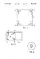
- FIG. lis a perspective view of an x ray inspection system that may be used in accordance with the present invention.
- FIG. 2is an exploded side view of an exemplary MLB panel, each of the individual layers being spaced apart for illustration purposes.
- FIG. 3is an exemplary projection view of the overlapping solder pads in a vertical stack.
- FIG. 4is a view in the x-y plane of an exemplary MLB panel.
- FIG. 5is a top view of an exemplary fixture as secured to the sample tray.
- FIG. 6is an exemplary field of view x-ray image visible in the, image display showing a fixture hole and the corresponding fiducial pad.
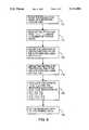
- FIG. 7is a block diagram of the learn sequence in the method of the present invention.
- FIG. 8is a block diagram of the inspect sequence in the method of the present invention.
- the x-ray inspection system 10comprises a computer 12, a computer display 14, a computer keyboard 16, an image processing unit 18, an image display 20, a control panel 22, and a sample tray 24.
- the computer 12is programmed to "learn” a fixture and “inspect” an MLB panel according to the steps that are more fully explained below.
- the computer display 14is used to view various menus that the user uses during operation of the system 10, and various prompts also appear on the display 14.
- the keyboard 16is used to move the user through the various menus and enter parameter values that the system 10 uses to "learn" all of the information it will require to automatically inspect MLB panels.
- the image processing unit 18records an x-ray image of an MLB panel positioned upon the sample tray 24.
- the image display 20displays the MLB panel that is being inspected and is used further to help “teach” the system 10 what it needs to "learn” about each MLB panel for later inspection.
- the control panel 22provides the basic controls to manipulate the system 10, including displays and readouts, a joystick to position the sample tray 24, x-ray controls, and camera motion controls.
- FIG. 2shows an exploded view of an exemplary MLB panel 26 having a plurality of layers 28, each of the layers 28 being spaced apart for illustration purposes. Electrical paths on the individual layers 28 terminate in solder pads 30, 32, 34 and 36. The solder pads 30, 32, 34, and 36 from the respective layers 28 are arranged in vertical stacks in order that electrical connections may be made between the different layers. Such connections are formed by drilling holes through the vertically arranged pads 30, 32, 34, 36 and then plating the holes with an electrically conductive material such as solder. The actual number of holes that are drilled through sets of vertically arranged solder pads for a particular panel may be in the hundreds or thousands.
- the number and size of the layers 28will vary depending upon the end use, as will the number and location of the solder pads 30, 32, 34, and 36. It is further to be understood that the size of the solder pads 30, 32, 34, and 36 are exaggerated herein for illustration purposes.
- the layers 28are designated as being in an x-y plane and the pads 30, 32, 34, or 36 are stacked in a z-axis. Due to the steps in the lamination process, stacks of vertically adjacent solder pads 30, 32, 34, or 36 may be misregistered from one another. Such misregistration of pads is shown in FIG. 3, which shows an enlarged projection view of overlapping pads 38A, 38B, and 38C of a vertical stack from a three-layer circuit board.
- an effective drill target 40(shown cross-hatched) that represents the common overlapping area of the pads 38A, 38B, and 38C.
- the hole that is to be drilled through the pads 38A, 38B, and 38Cmust be drilled within the effective drill target 40 in order to provide the proper electrical connection.
- the MLB panel 26is built according to a "blueprint". If the solder pads 38A, 38B, and 38C could be built exactly according to the blueprint, there would be no misregistration of the layers 28 and the solder pads 38A, 38B, and 38C would be in perfect vertical alignment at the locations as specified by the blueprint, referred to herein as the blueprint coordinates of the solder pads. Further, if there was no misregistration of the layers 28, then the ideal drill coordinates would be the same as the blueprint coordinates of the solder pads.
- each MLB panelalso has fiducial pads 39 at various locations on the MLB panel, as highlighted in a panel 41 in FIG. 4.
- Fiducial pads 39are located as reference points on the panel 41 and are staggered so that there is no overlap of fiducial pads 39 from one layer to another.
- the fiducial pads 39are grouped closely together in arrangements known as coupons 43 such that there is one fiducial pad 39 from each of the different layers in close proximity without overlapping.
- the panel 41 of FIG. 4as an example, the panel 41 has four layers.
- the panel 41has four coupons 43 positioned near each of the corners of the panel 31.
- Each of the coupons 43has four fiducial pads 39, each pad 39 being located on a different layer.
- the fiducial pads 39 of a particular couponare therefore configured in a pattern in order that each layer may be uniquely identified.
- the panel 41also has tooling holes 45 located in each of the corners of the panel 41. It is to be understood that the size of the fiducial pads 39 is exaggerated herein for illustration purposes. It is to be also understood that the depiction of FIG. 3 is meant to highlight the fiducial pads 39 and the tooling holes 45, though there would also be solder pads across the x-y face of the panel 41 that are to be drilled to provide electrical connections.
- the fiducial pads 39are also built to be located according to blueprint coordinates, though the fiducial pads 39 are subject to misregistration in the same manner as the solder pads 38A, 38B, and 38C.
- a fixture 42is carefully prepared with fixture holes 44 that correspond to the x-y blueprint locations of the fiducial pads 39 of the panel 41.
- the fixture 42is shown in FIG. 5.
- the top of the fixture 42is shown as it is positioned and secured on the sample tray 24 of the system 10.
- the sample tray 24is mounted upon a table (not shown) and movable in x and y directions by motors (not shown). Movement of the sample tray 24 is necessary to examine different fields of view of the MLB panel.
- the fixture 42has tooling pins 48 in each of the corners of the fixture 42 that engage with the tooling holes 45 of the MLB panel 41 in which the drill target locations are to be determined. The engagement of the tooling pins 48 with the tooling holes 45 allows the MLB panel to be held rigidly in an absolute position relative to the fixture 42.
- FIG. 1shows a door 52 to the chamber 50 in an open position and the sample tray 24 slid outward for access to the operator.
- the sample tray 24is slid within the chamber 50 and the door 52 is in a closed position.
- a camera(not shown) is contained within the chamber 50.
- FIG. 6shows a typical field of view containing one of the fixture holes 44 and fiducial pads 39 as would be seen at the image display 20.
- the fixture holes 44 of the fixture 42are larger than the fiducial pads 39 of the MLB panel 41.
- each of the fiducial pads 39are contained within the boundaries of a respective fixture hole 44.
- a software routine of the computer 12then computes the offset between the fixture hole 44 and the fiducial pad 39 visible in the field of view, such as by first thresholding the image to separate the outline of the respective fixture hole 44 from the fiducial pad 39, and then computing the centroid of the separate images.
- the offset informationis then sent to a drilling machine which drills the vertical stacks of the solder pads of the MLB panel in accordance with the offset.
- FIG. 7may be considered a "learn” sequence and FIG. 8 may be considered an “inspect” sequence.
- the ideal, or blueprint, coordinates relative to a fixed reference point for each of the fixture holes 44 of the fixture 42are entered and stored within the computer 12 at 100.
- the blueprint coordinates of the fixture holes 44 and the blueprint coordinates of the fiducial pads 39would be the same inasmuch as they are correspondent points.
- the table coordinates of the fixture holes 42are entered into the computer 12 at 104.
- the inspect sequencefollows and begins by mounting of the MLB panel 41 upon the fixture 42 at 110 by engagement of the tooling pins 48 and the tooling holes 45, such as described above.
- the centroid of the fixture hole 44 and the respective centroid of the fiducial pad 39is obtained at 116 and 118.
- the ability to determine the centroids of either the fixture hole 44 or the fiducial pad 39is known in the art and described in articles by E.R. Davies, "A Modified Hough Scheme for General Circle Location,” Pattern Recognition Letters, vol. 7 (Jan., 1988), pp.
- the movement to the field of views of the first and subsequent patterns 44is accomplished by the computer 12 recalling the table coordinates obtained at 104.
- the x-coordinate offsetis obtained at 120 by subtracting the x-coordinate of the fiducial pad 39 from the x-coordinate of the fixture hole 44.
- the y-coordinate offsetis further obtained at 120 by subtracting the y-coordinate of the fiducial pad 39 from the y-coordinate of the fixture hole 44.
- a "measured location”is then obtained at 120 by adding the x and y offsets to the ideal, or blueprint, coordinates that were stored by the computer 12 at 100.
- the steps 114, 116, 118, and 120are then repeated for all of the fixture holes 44 and the associated fiducial pads 39 that may be viewed within.
- the offsets and measured locations that are thus obtainedrepresent a sampling from each of the different layers from different locations across the x-y face of the MLB panel 41.
- the fiducial pads 39are often from coupons 43 located in the four corners of the panel 41 because the four corners usually represent the "worst case" misregistration on the panel 41.
- the valuesmay be analyzed by a Best Fit algorithm.
- the offsetsare thus fitted to produce a single offset value that may be added to each of the ideal, or blueprint, coordinates of the solder pads to produce corrections to the ideal drill coordinates.
- alternate Best Fit algorithmsit is possible to fit not only to x and y coordinates, but also to include corrections to rotational ( ⁇ ) misregistration of the layers of the panel 41. For such a case, there are as many offset values as there drill coordinates.
- fiducial padis therefore broadly defined as any reference point or fiducial that may be used in the manner such as the fiducial pads specified herein.
Landscapes
- Engineering & Computer Science (AREA)
- Manufacturing & Machinery (AREA)
- Microelectronics & Electronic Packaging (AREA)
- Mechanical Engineering (AREA)
- Analysing Materials By The Use Of Radiation (AREA)
Abstract
Description
Claims (7)
Priority Applications (1)
| Application Number | Priority Date | Filing Date | Title |
|---|---|---|---|
| US07/462,393US5111406A (en) | 1990-01-05 | 1990-01-05 | Method for determining drill target locations in a multilayer board panel |
Applications Claiming Priority (1)
| Application Number | Priority Date | Filing Date | Title |
|---|---|---|---|
| US07/462,393US5111406A (en) | 1990-01-05 | 1990-01-05 | Method for determining drill target locations in a multilayer board panel |
Publications (1)
| Publication Number | Publication Date |
|---|---|
| US5111406Atrue US5111406A (en) | 1992-05-05 |
Family
ID=23836284
Family Applications (1)
| Application Number | Title | Priority Date | Filing Date |
|---|---|---|---|
| US07/462,393Expired - LifetimeUS5111406A (en) | 1990-01-05 | 1990-01-05 | Method for determining drill target locations in a multilayer board panel |
Country Status (1)
| Country | Link |
|---|---|
| US (1) | US5111406A (en) |
Cited By (31)
| Publication number | Priority date | Publication date | Assignee | Title |
|---|---|---|---|---|
| WO1994008443A1 (en)* | 1992-09-29 | 1994-04-14 | Berg N Edward | Method and apparatus for fabricating printed circuit boards |
| US5529441A (en)* | 1994-02-28 | 1996-06-25 | Cybernetics Products, Inc. | Drill coordinate optimization for multi-layer printed circuit board |
| US5661654A (en)* | 1994-04-28 | 1997-08-26 | Toshiba Kikai Kabushiki Kaisha | Method of correcting error in mounting workpiece and apparatus therefor |
| US5741096A (en)* | 1995-11-30 | 1998-04-21 | The Boeing Company | Line-laser assisted alignment apparatus |
| US6030154A (en)* | 1998-06-19 | 2000-02-29 | International Business Machines Corporation | Minimum error algorithm/program |
| US6199290B1 (en) | 1999-07-30 | 2001-03-13 | Excellon Automation Co. | Method and apparatus for automatic loading and registration of PCBs |
| US6232559B1 (en) | 1998-01-05 | 2001-05-15 | International Business Machines Corporation | Multi-layer printed circuit board registration |
| US6276676B1 (en) | 1999-07-30 | 2001-08-21 | Excellon Automation Company | Manual registration pin alignment system |
| US6283681B1 (en)* | 1997-11-18 | 2001-09-04 | Borgotec Tecnologie Autom Spa | Method and device for aligning a workpiece on a machine tool table |
| US6297458B1 (en) | 1999-04-14 | 2001-10-02 | Dell Usa, L.P. | Printed circuit board and method for evaluating the inner layer hole registration process capability of the printed circuit board manufacturing process |
| US20010026638A1 (en)* | 2000-03-28 | 2001-10-04 | Katsuya Sangu | Positioning apparatus used in a process for producing multi-layered printed circuit board and method of using the same |
| US20020050055A1 (en)* | 2000-10-26 | 2002-05-02 | Nitto Denko Corporation | Boring method for circuit board |
| US20030044248A1 (en)* | 2000-10-11 | 2003-03-06 | Toshihiro Nishii | Circuit board production method and circuit board production data |
| US20030130826A1 (en)* | 2002-01-08 | 2003-07-10 | International Business Machines Corporation | Model for modifying drill data to predict hole locations in a panel structure |
| US6668448B2 (en)* | 1999-05-12 | 2003-12-30 | Microconnex Corp. | Method of aligning features in a multi-layer electrical connective device |
| EP1441874A1 (en) | 2001-10-09 | 2004-08-04 | Chromalloy Gas Turbine Corporation | Method for removing coating material from a cooling hole of a gas turbine engine component |
| US20040222197A1 (en)* | 1996-11-20 | 2004-11-11 | Ibiden Co., Ltd. | Laser machining apparatus, and apparatus and method for manufacturing a multilayered printed wiring board |
| US20050263498A1 (en)* | 1996-11-20 | 2005-12-01 | Ibiden Co., Ltd. | Ceramic heater |
| US20050271113A1 (en)* | 2004-06-07 | 2005-12-08 | Song Yoon K | High thermal conductivity vertical cavity surface emitting laser (VCSEL) |
| WO2006040088A3 (en)* | 2004-10-08 | 2006-07-27 | Feinfocus Gmbh | Drilling device for drilling contact holes for assembling contact surfaces of a multilayer circuit boards |
| US20060274935A1 (en)* | 2000-03-01 | 2006-12-07 | Delarosa Eugene A | Method for measuring registration of overlapping material layers of an integrated circuit |
| US20070098248A1 (en)* | 2005-10-28 | 2007-05-03 | Yasutaka Toyoda | Pattern matching apparatus and semiconductor inspection system using the same |
| DE102005053202A1 (en)* | 2005-11-08 | 2007-05-10 | Comet Gmbh | Apparatus for preparing a multilayer printed circuit board for drilling via holes |
| US20070257012A1 (en)* | 2006-05-02 | 2007-11-08 | Wile Donald E | Method and apparatus for laser processing |
| US20070276629A1 (en)* | 2006-04-07 | 2007-11-29 | United Technologies Corporation | System and method for inspection of hole location on turbine airfoils |
| US7619434B1 (en)* | 2004-12-01 | 2009-11-17 | Cardiac Pacemakers, Inc. | System for multiple layer printed circuit board misregistration testing |
| CN102189282A (en)* | 2010-03-12 | 2011-09-21 | 宏恒胜电子科技(淮安)有限公司 | System and method for making short slot hole of circuit board |
| US8275479B1 (en)* | 2009-10-21 | 2012-09-25 | The Boeing Company | Method and apparatus for deburring splices |
| JP2018046132A (en)* | 2016-09-14 | 2018-03-22 | 株式会社ムラキ | Automatic transport device applied to multilayer circuit board reference boring machine |
| US20210360793A1 (en)* | 2020-05-14 | 2021-11-18 | Skybrain Vermögensverwaltungs Gmbh | Machining Station and Method for Machining Workpieces |
| CN118748150A (en)* | 2024-06-27 | 2024-10-08 | 奥芯半导体科技(太仓)有限公司 | Method for drilling holes in substrate and packaging substrate |
Citations (8)
| Publication number | Priority date | Publication date | Assignee | Title |
|---|---|---|---|---|
| US3573455A (en)* | 1968-09-13 | 1971-04-06 | Ibm | Examination of articles by x-rays |
| US4481533A (en)* | 1981-11-27 | 1984-11-06 | Lenkeit Industries, Inc. | Method and apparatus for successively positioning sheets of material with precision for punching aligning holes in the sheets enabling the sheets to be used in the manufacture of composite circuit boards |
| US4536239A (en)* | 1983-07-18 | 1985-08-20 | Nicolet Instrument Corporation | Multi-layer circuit board inspection system |
| US4668982A (en)* | 1985-06-17 | 1987-05-26 | The Perkin-Elmer Corporation | Misregistration/distortion correction scheme |
| US4720798A (en)* | 1985-04-16 | 1988-01-19 | Protocad, Inc. | Process for use in rapidly producing printed circuit boards using a computer controlled plotter |
| US4790694A (en)* | 1986-10-09 | 1988-12-13 | Loma Park Associates | Method and system for multi-layer printed circuit board pre-drill processing |
| US4829375A (en)* | 1986-08-29 | 1989-05-09 | Multiline Technology, Inc. | Method for punching in printed circuit board laminates and related apparatus and articles of manufacture |
| US4898636A (en)* | 1989-05-04 | 1990-02-06 | Rigling Walter S | Multilayer printed wiring registration method and apparatus |
- 1990
- 1990-01-05USUS07/462,393patent/US5111406A/ennot_activeExpired - Lifetime
Patent Citations (8)
| Publication number | Priority date | Publication date | Assignee | Title |
|---|---|---|---|---|
| US3573455A (en)* | 1968-09-13 | 1971-04-06 | Ibm | Examination of articles by x-rays |
| US4481533A (en)* | 1981-11-27 | 1984-11-06 | Lenkeit Industries, Inc. | Method and apparatus for successively positioning sheets of material with precision for punching aligning holes in the sheets enabling the sheets to be used in the manufacture of composite circuit boards |
| US4536239A (en)* | 1983-07-18 | 1985-08-20 | Nicolet Instrument Corporation | Multi-layer circuit board inspection system |
| US4720798A (en)* | 1985-04-16 | 1988-01-19 | Protocad, Inc. | Process for use in rapidly producing printed circuit boards using a computer controlled plotter |
| US4668982A (en)* | 1985-06-17 | 1987-05-26 | The Perkin-Elmer Corporation | Misregistration/distortion correction scheme |
| US4829375A (en)* | 1986-08-29 | 1989-05-09 | Multiline Technology, Inc. | Method for punching in printed circuit board laminates and related apparatus and articles of manufacture |
| US4790694A (en)* | 1986-10-09 | 1988-12-13 | Loma Park Associates | Method and system for multi-layer printed circuit board pre-drill processing |
| US4898636A (en)* | 1989-05-04 | 1990-02-06 | Rigling Walter S | Multilayer printed wiring registration method and apparatus |
Non-Patent Citations (12)
| Title |
|---|
| "MU 90 S: Controle des Circuits Imprimes", Usine Nouvell, issue #16, Apr. 21, 1988. |
| E. R. Davies, "A Modified Hough Scheme for General Circle Location", Pattern Recognition Letters, vol. 7, pp. 37-43 (1988). |
| E. R. Davies, "Circularity--A New Principle Underlying the Design of Accurate Edge Orientation Operators", Image and Vision Computing, vol. 2, No. 3, pp. 134-142. |
| E. R. Davies, A Modified Hough Scheme for General Circle Location , Pattern Recognition Letters, vol. 7, pp. 37 43 (1988).* |
| E. R. Davies, Circularity A New Principle Underlying the Design of Accurate Edge Orientation Operators , Image and Vision Computing , vol. 2, No. 3, pp. 134 142.* |
| K. Bieneman, "Drill Position Optimization for MLB Process Control", PC FAB, Mar. 1988, pp. 45-50. This is a later version of the above-listed paper presented at the Printed Circuit Fabrication Exposition. |
| K. Bieneman, "Drill Position Optimization Techniques Using Real-time X-ray Imaging", Nicolet Instrument Corporation, presented at the Printed Circuit Fabrication Exposition, Minneapolis, MN Sep. 15, 1987. |
| K. Bieneman, Drill Position Optimization for MLB Process Control , PC FAB, Mar. 1988, pp. 45 50. This is a later version of the above listed paper presented at the Printed Circuit Fabrication Exposition.* |
| K. Bieneman, Drill Position Optimization Techniques Using Real time X ray Imaging , Nicolet Instrument Corporation, presented at the Printed Circuit Fabrication Exposition, Minneapolis, MN Sep. 15, 1987.* |
| MU 90 S: Controle des Circuits Imprimes , Usine Nouvell , issue 16, Apr. 21, 1988.* |
| PA 120 Operations Manual, Nicolet Instrument Corporation, release date Jul. 17, 1989.* |
| PA-120 Operations Manual, Nicolet Instrument Corporation, release date Jul. 17, 1989. |
Cited By (52)
| Publication number | Priority date | Publication date | Assignee | Title |
|---|---|---|---|---|
| WO1994008443A1 (en)* | 1992-09-29 | 1994-04-14 | Berg N Edward | Method and apparatus for fabricating printed circuit boards |
| US5529441A (en)* | 1994-02-28 | 1996-06-25 | Cybernetics Products, Inc. | Drill coordinate optimization for multi-layer printed circuit board |
| US5661654A (en)* | 1994-04-28 | 1997-08-26 | Toshiba Kikai Kabushiki Kaisha | Method of correcting error in mounting workpiece and apparatus therefor |
| US5741096A (en)* | 1995-11-30 | 1998-04-21 | The Boeing Company | Line-laser assisted alignment apparatus |
| US20040222197A1 (en)* | 1996-11-20 | 2004-11-11 | Ibiden Co., Ltd. | Laser machining apparatus, and apparatus and method for manufacturing a multilayered printed wiring board |
| US20060138098A1 (en)* | 1996-11-20 | 2006-06-29 | Ibiden Co., Ltd. | Laser machining apparatus, and apparatus and method for manufacturing a multilayered printed wiring board |
| US7462802B2 (en) | 1996-11-20 | 2008-12-09 | Ibiden Co., Ltd. | Laser machining apparatus, and apparatus and method for manufacturing a multilayered printed wiring board |
| US7456372B2 (en)* | 1996-11-20 | 2008-11-25 | Ibiden Co., Ltd. | Laser machining apparatus, and apparatus and method for manufacturing a multilayered printed wiring board |
| US20050263498A1 (en)* | 1996-11-20 | 2005-12-01 | Ibiden Co., Ltd. | Ceramic heater |
| US7667160B2 (en) | 1996-11-20 | 2010-02-23 | Ibiden Co., Ltd | Laser machining apparatus, and apparatus and method for manufacturing a multilayered printed wiring board |
| US7462801B1 (en) | 1996-11-20 | 2008-12-09 | Ibiden Co., Ltd. | Laser machining apparatus, and apparatus and method for manufacturing a multilayered printed wiring board |
| US7732732B2 (en)* | 1996-11-20 | 2010-06-08 | Ibiden Co., Ltd. | Laser machining apparatus, and apparatus and method for manufacturing a multilayered printed wiring board |
| US6283681B1 (en)* | 1997-11-18 | 2001-09-04 | Borgotec Tecnologie Autom Spa | Method and device for aligning a workpiece on a machine tool table |
| US6662441B2 (en) | 1998-01-05 | 2003-12-16 | International Business Machines Corporation | Method for making multi-layer printed circuit board registration |
| US6232559B1 (en) | 1998-01-05 | 2001-05-15 | International Business Machines Corporation | Multi-layer printed circuit board registration |
| US6030154A (en)* | 1998-06-19 | 2000-02-29 | International Business Machines Corporation | Minimum error algorithm/program |
| US6297458B1 (en) | 1999-04-14 | 2001-10-02 | Dell Usa, L.P. | Printed circuit board and method for evaluating the inner layer hole registration process capability of the printed circuit board manufacturing process |
| US6668448B2 (en)* | 1999-05-12 | 2003-12-30 | Microconnex Corp. | Method of aligning features in a multi-layer electrical connective device |
| US6199290B1 (en) | 1999-07-30 | 2001-03-13 | Excellon Automation Co. | Method and apparatus for automatic loading and registration of PCBs |
| US6276676B1 (en) | 1999-07-30 | 2001-08-21 | Excellon Automation Company | Manual registration pin alignment system |
| US20060274935A1 (en)* | 2000-03-01 | 2006-12-07 | Delarosa Eugene A | Method for measuring registration of overlapping material layers of an integrated circuit |
| US6870952B2 (en)* | 2000-03-28 | 2005-03-22 | Adtec Engineering Co., Ltd. | Positioning apparatus used in a process for producing multi-layered printed circuit board and method of using the same |
| US20010026638A1 (en)* | 2000-03-28 | 2001-10-04 | Katsuya Sangu | Positioning apparatus used in a process for producing multi-layered printed circuit board and method of using the same |
| US20030044248A1 (en)* | 2000-10-11 | 2003-03-06 | Toshihiro Nishii | Circuit board production method and circuit board production data |
| US7097394B2 (en)* | 2000-10-11 | 2006-08-29 | Matsushita Electric Industrial Co., Ltd. | Circuit board production method and circuit board production data |
| US20020050055A1 (en)* | 2000-10-26 | 2002-05-02 | Nitto Denko Corporation | Boring method for circuit board |
| US7006879B2 (en)* | 2000-10-26 | 2006-02-28 | Nitto Denko Corporation | Boring method for circuit board |
| EP1441874A1 (en) | 2001-10-09 | 2004-08-04 | Chromalloy Gas Turbine Corporation | Method for removing coating material from a cooling hole of a gas turbine engine component |
| US20060253270A1 (en)* | 2002-01-08 | 2006-11-09 | Nguyen Manh-Quan T | Model for modifying drill data to predict hole locations in a panel structure |
| US20030130826A1 (en)* | 2002-01-08 | 2003-07-10 | International Business Machines Corporation | Model for modifying drill data to predict hole locations in a panel structure |
| US7089160B2 (en) | 2002-01-08 | 2006-08-08 | International Business Machines Corporation | Model for modifying drill data to predict hole locations in a panel structure |
| US20050271113A1 (en)* | 2004-06-07 | 2005-12-08 | Song Yoon K | High thermal conductivity vertical cavity surface emitting laser (VCSEL) |
| WO2006040088A3 (en)* | 2004-10-08 | 2006-07-27 | Feinfocus Gmbh | Drilling device for drilling contact holes for assembling contact surfaces of a multilayer circuit boards |
| US20070256298A1 (en)* | 2004-10-08 | 2007-11-08 | Alfred Reinhold | Boring device for boring via holes for connecting contact regions of multilayer printed circuit boards |
| US20100019789A1 (en)* | 2004-12-01 | 2010-01-28 | Orrin Paul Lorenz | System for multiple layer printed circuit board misregistration testing |
| US7619434B1 (en)* | 2004-12-01 | 2009-11-17 | Cardiac Pacemakers, Inc. | System for multiple layer printed circuit board misregistration testing |
| US7982487B2 (en) | 2004-12-01 | 2011-07-19 | Cardiac Pacemakers, Inc. | System for multiple layer printed circuit board misregistration testing |
| US20070098248A1 (en)* | 2005-10-28 | 2007-05-03 | Yasutaka Toyoda | Pattern matching apparatus and semiconductor inspection system using the same |
| US7991218B2 (en)* | 2005-10-28 | 2011-08-02 | Hitachi High-Technologies Corporation | Pattern matching apparatus and semiconductor inspection system using the same |
| DE102005053202A1 (en)* | 2005-11-08 | 2007-05-10 | Comet Gmbh | Apparatus for preparing a multilayer printed circuit board for drilling via holes |
| US20070276629A1 (en)* | 2006-04-07 | 2007-11-29 | United Technologies Corporation | System and method for inspection of hole location on turbine airfoils |
| US7574035B2 (en)* | 2006-04-07 | 2009-08-11 | United Technologies Corporation | System and method for inspection of hole location on turbine airfoils |
| US7834293B2 (en)* | 2006-05-02 | 2010-11-16 | Electro Scientific Industries, Inc. | Method and apparatus for laser processing |
| US20070257012A1 (en)* | 2006-05-02 | 2007-11-08 | Wile Donald E | Method and apparatus for laser processing |
| US8275479B1 (en)* | 2009-10-21 | 2012-09-25 | The Boeing Company | Method and apparatus for deburring splices |
| CN102189282A (en)* | 2010-03-12 | 2011-09-21 | 宏恒胜电子科技(淮安)有限公司 | System and method for making short slot hole of circuit board |
| CN102189282B (en)* | 2010-03-12 | 2013-03-06 | 宏恒胜电子科技(淮安)有限公司 | System and method for making short slot hole of circuit board |
| JP2018046132A (en)* | 2016-09-14 | 2018-03-22 | 株式会社ムラキ | Automatic transport device applied to multilayer circuit board reference boring machine |
| US20210360793A1 (en)* | 2020-05-14 | 2021-11-18 | Skybrain Vermögensverwaltungs Gmbh | Machining Station and Method for Machining Workpieces |
| US11963305B2 (en)* | 2020-05-14 | 2024-04-16 | Skybrain Vermögensverwaltungs Gmbh | Machining station and method for machining workpieces |
| US12324104B2 (en)* | 2020-05-14 | 2025-06-03 | Skybrain Vermögensverwaltungs Gmbh | Method for machining workpieces |
| CN118748150A (en)* | 2024-06-27 | 2024-10-08 | 奥芯半导体科技(太仓)有限公司 | Method for drilling holes in substrate and packaging substrate |
Similar Documents
| Publication | Publication Date | Title |
|---|---|---|
| US5111406A (en) | Method for determining drill target locations in a multilayer board panel | |
| EP0264243B1 (en) | Method and system for multi-layer printed circuit board pre-drill processing | |
| US5377404A (en) | Method for fabricating a multi-layer printed circuit board | |
| US5529441A (en) | Drill coordinate optimization for multi-layer printed circuit board | |
| JP4542046B2 (en) | Drilling method and drilling device | |
| US7982487B2 (en) | System for multiple layer printed circuit board misregistration testing | |
| US5541856A (en) | X-ray inspection system | |
| US5008619A (en) | Multilevel circuit board precision positioning | |
| US7181089B2 (en) | Method and apparatus for searching for fiducial marks, and method of detecting positions of the fiducial marks | |
| US6496270B1 (en) | Method and system for automatically generating reference height data for use in a three-dimensional inspection system | |
| US4708545A (en) | Method for drilling reference holes in multi-layer printed wiring board assembly | |
| US7283660B2 (en) | Multi-layer printed circuit board fabrication system and method | |
| US20090000814A1 (en) | Multiple layer printed circuit board having misregistration testing pattern | |
| JPH0413880B2 (en) | ||
| US20020118350A1 (en) | Method and apparatus for registration control in production by imaging | |
| US6662441B2 (en) | Method for making multi-layer printed circuit board registration | |
| KR20190135422A (en) | Method for calibrating an apparatus for mounting components | |
| KR920003403B1 (en) | Mounting device of flat package type IC | |
| KR100509340B1 (en) | Method and device for testing printed circuit boards with a parallel tester | |
| JP3550462B2 (en) | Drilling method, drilling device, hole position detecting method, and hole position detecting device for plate-shaped work | |
| JP2833402B2 (en) | Inspection method of electrode plate to be inspected | |
| US4966520A (en) | Method of positioning objects to be measured | |
| KR101825832B1 (en) | Automatic handling device for applied in a multilayer circuit board drill machine | |
| US6252414B1 (en) | Method and apparatus for testing circuits having different configurations with a single test fixture | |
| JP2001315299A (en) | Screen mask alignment method for screen printing |
Legal Events
| Date | Code | Title | Description |
|---|---|---|---|
| AS | Assignment | Owner name:NICOLET INSTRUMENT CORPORATION, 5225 VERONA RD., M Free format text:ASSIGNMENT OF ASSIGNORS INTEREST.;ASSIGNORS:ZACHMAN, JULIE C.;KUNTZ, ROBERT A.;SMITH, STEVEN R.;AND OTHERS;REEL/FRAME:005261/0569;SIGNING DATES FROM 19900216 TO 19900226 | |
| STCF | Information on status: patent grant | Free format text:PATENTED CASE | |
| FPAY | Fee payment | Year of fee payment:4 | |
| AS | Assignment | Owner name:THERMOSPECTRA CORPORATION, MASSACHUSETTS Free format text:ASSIGNMENT OF ASSIGNORS INTEREST;ASSIGNOR:NICOLET INSTRUMENT CORPORATION;REEL/FRAME:008876/0523 Effective date:19970519 | |
| FPAY | Fee payment | Year of fee payment:8 | |
| AS | Assignment | Owner name:GENRAD, INC., MASSACHUSETTS Free format text:ASSIGNMENT OF ASSIGNORS INTEREST;ASSIGNOR:THERMOSPECTRA CORPORATION;REEL/FRAME:010848/0872 Effective date:20000324 | |
| AS | Assignment | Owner name:TERADYNE, INC., MASSACHUSETTS Free format text:ASSIGNMENT OF ASSIGNORS INTEREST;ASSIGNOR:GENRAD, INC.;REEL/FRAME:013101/0329 Effective date:20020710 | |
| AS | Assignment | Owner name:THERMOSPECTRA CORPORATION, MASSACHUSETTS Free format text:ASSIGNMENT OF ASSIGNORS INTEREST;ASSIGNOR:NICOLET IMAGING SYSTEMS, INC.;REEL/FRAME:013288/0013 Effective date:20021119 | |
| FPAY | Fee payment | Year of fee payment:12 | |
| FEPP | Fee payment procedure | Free format text:PAYOR NUMBER ASSIGNED (ORIGINAL EVENT CODE: ASPN); ENTITY STATUS OF PATENT OWNER: LARGE ENTITY Free format text:PAYER NUMBER DE-ASSIGNED (ORIGINAL EVENT CODE: RMPN); ENTITY STATUS OF PATENT OWNER: LARGE ENTITY | |
| AS | Assignment | Owner name:BANK OF AMERICA, N.A., AS ADMINISTRATIVE AGENT, TE Free format text:NOTICE OF GRANT OF SECURITY INTEREST IN PATENTS;ASSIGNOR:TERADYNE, INC.;REEL/FRAME:021912/0762 Effective date:20081114 Owner name:BANK OF AMERICA, N.A., AS ADMINISTRATIVE AGENT,TEX Free format text:NOTICE OF GRANT OF SECURITY INTEREST IN PATENTS;ASSIGNOR:TERADYNE, INC.;REEL/FRAME:021912/0762 Effective date:20081114 | |
| AS | Assignment | Owner name:TERADYNE, INC, MASSACHUSETTS Free format text:RELEASE BY SECURED PARTY;ASSIGNOR:BANK OF AMERICA, N.A.;REEL/FRAME:022668/0750 Effective date:20090427 Owner name:TERADYNE, INC,MASSACHUSETTS Free format text:RELEASE BY SECURED PARTY;ASSIGNOR:BANK OF AMERICA, N.A.;REEL/FRAME:022668/0750 Effective date:20090427 |