US5107231A - Dielectric waveguide to TEM transmission line signal launcher - Google Patents
Dielectric waveguide to TEM transmission line signal launcherDownload PDFInfo
- Publication number
- US5107231A US5107231AUS07/357,345US35734589AUS5107231AUS 5107231 AUS5107231 AUS 5107231AUS 35734589 AUS35734589 AUS 35734589AUS 5107231 AUS5107231 AUS 5107231A
- Authority
- US
- United States
- Prior art keywords
- conductive
- dielectric waveguide
- waveguide
- dielectric
- ground plane
- Prior art date
- Legal status (The legal status is an assumption and is not a legal conclusion. Google has not performed a legal analysis and makes no representation as to the accuracy of the status listed.)
- Expired - Fee Related
Links
Images
Classifications
- H—ELECTRICITY
- H01—ELECTRIC ELEMENTS
- H01P—WAVEGUIDES; RESONATORS, LINES, OR OTHER DEVICES OF THE WAVEGUIDE TYPE
- H01P5/00—Coupling devices of the waveguide type
- H01P5/08—Coupling devices of the waveguide type for linking dissimilar lines or devices
- H01P5/10—Coupling devices of the waveguide type for linking dissimilar lines or devices for coupling balanced lines or devices with unbalanced lines or devices
- H01P5/1022—Transitions to dielectric waveguide
Definitions
- the present inventionrelates generally to improvements in high frequency communication systems and particularly to signal launchers for coupling signals to and from dielectric insular and image waveguide transmission lines to TEM mode transmission lines.
- Waveguide transmission linesare widely used to channel the flow of high frequency electromagnetic energy.
- Common transmission linesare coaxial transmission lines, and planar transmission lines such as microstrip transmission lines, and dielectric waveguide transmission lines with ground plane.
- Dielectric waveguidesincludes image and insular waveguide transmission lines.
- Image and insular waveguide transmission linesexhibit low loss at high frequencies such as in the 10 GHz to 300 GHz frequency range, and are therefore highly suitable for applications at such high frequencies.
- dielectric waveguideshave been difficult to integrate with active devices.
- Microstrip structures in which the electromagnetic energy propagates in a TEM modehave high loss at such high frequencies, but are highly suitable for integration of active devices.
- a high efficiency signal launcher for coupling between dielectric waveguides and microstrip structures, as well as other TEM structures, such as coaxial transmission lineswould be advantageous and would facilitate construction of hybrid microwave and millimeter wave circuitry.
- apparatusfor a mode conversion signal launcher for coupling signals of a predetermined wavelength between a dielectric waveguide and a TEM mode transmission line.
- the launchercomprises a conductive ground plane and an elongated high permittivity dielectric waveguide of predetermined cross section adjacent to the conductive ground plane.
- a TEM mode transmission lineis provided having an elongated conducting waveguide portion fixed adjacent to a portion of the dielectric waveguide such that the dielectric waveguide and conductive portions form a distributed coupling region having a length of least two times the predetermined wavelength.
- FIGS. 1A, 1B, 1C, and 1Dare illustrations of several prior art waveguide structures.
- FIGS. 2Ais a schematic representation illustrating a tapered signal launcher according to the invention.
- FIGS. 2Bis a schematic representation illustrating a tapered signal launcher coupled to a microstrip structure.
- FIGS. 2Cis a schematic representation illustrating an alternative tapered signal launcher structure coupled to a microstrip structure.
- FIGS. 2Dis a schematic representation illustrating a tapered signal launcher coupled to a coaxial transmission line.
- FIG. 2Eis a schematic representation illustrating an alternative shape to the metal conductive waveguide of the tapered launcher of FIG. 2A.
- FIG. 3is a schematic representation illustrating a parallel waveguide structure signal launcher according to the invention.
- FIG. 4is a schematic representation illustrating a crossed waveguide structure signal launcher according to the invention.
- FIG. 5is a schematic representation illustrating a straddled waveguide structure signal launcher according to the invention.
- FIG. 6is a schematic representation illustrating a dielectric waveguide microstrip mixer structure constructed using a tapered signal launcher structure according to the invention.
- FIG. 7Ais a schematic representation illustrating an abrupt coupling signal launcher coupled to a microstrip structure according to the invention.
- FIG. 7Bis a detailed blow up of a schematic representation illustrating an alternative abrupt coupling signal launcher coupled to a microstrip structure according to the invention.
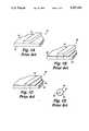
- FIG. 1Aillustrates a prior art dielectric image waveguide structure 10 comprising a conductive metal ground plane (image plane) in the form of a conductive plate 12.
- An elongated dielectric waveguide 14 having a rectangular or square cross-section and composed of high permittivity (e.g. 10) dielectric materialis mounted in intimate contact with the upper surface of the conductive image plate 12, as shown.
- a variation of the image dielectric waveguideis the insular dielectric waveguide structure 20 illustrated in FIG. IB.
- the insular waveguide structure 20comprises a conductive base plate 22 (ground plane) and a dielectric waveguide 24 composed of a high permittivity (e.g., 10) dielectric material such as ceramic, alumina, quartz, ceramic filled synthetic organic resin, etc., as in the image waveguide structure.
- a thin dielectric film 26 of low permittivity (e.g., less than 3) and low loss (e.g., loss tangent less than 0.001)such as a synthetic organic resin, e.g., polyethylene.
- the filmextends laterally beyond the sides of the dielectric waveguide 24 and is intimately connected to both the base plate 22 and the dielectric waveguide 24.
- dielectric waveguides 14,24have been illustrated as being rectangular in cross section, other shapes may be used including hemispherical, trapezoidal, triangular, hexagonal, and the like. Such insular dielectric waveguides are known in the art, and are described in detail in a patent to Knox, et al., issued Nov. 30, 1976, U.S. Pat. No. 3,995,238, which is hereby incorporated by reference.
- FIG. 1Cillustrates a microstrip structure 30 which comprises a conductive ground plane in the form of a conductive metal plate 32 with a dielectric layer 34 of various permittivities (e.g., typically 2.5 but as high as 10) affixed to the surface of the conductive plate 32.
- a conductive thin strip 36typically metal, is mounted on the surface of the dielectric layer 34, as shown.
- Resulting structuremay be fabricated in an integrated form with active device integrated directly with waveguide structures using the same dielectric and ground plane.
- FIG. 1Dillustrates a coaxial transmission line structure 40 which comprises an outer conductor 42 and an inner conductor 44 which is surrounded by the outer conductor.
- a dielectric material 46separates the inner conductor and the outer conductor.
- microstrip structuresprovide the basis for integrating active devices, they suffer from high loss and low Q at high frequencies (i.e., above 10 GHz). Further, microstrip permits the advantage of maintaining the purity of the propagation mode to the very contacts of the active devices in high frequency circuits so that impedance matching can be effectively and reproducible achieved. Conversely, dielectric waveguide structures are difficult to integrate with active devices (i.e., diodes, transistors, etc.) but exhibit much lower loss and higher Q characteristics at high frequencies. By combining these advantages of microstrip to permit integration of active devices and the low loss, high Q characteristics of dielectric waveguides, substantial circuit improvements can be obtained. However, since electromagnetic energy propagates in different modes in the dielectric waveguides than in microstrip waveguides, any interconnection between them requires a mode converting signal launcher.
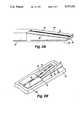
- FIG. 2Aillustrates a tapered structure mode converting signal launcher 50 which may function, for example, as a launcher for converting E 11 ⁇ mode to TEM mode.
- the tapered launcher 50converts the E 11 ⁇ mode to the TEM mode through the interaction of a thin conductive strip 52 on a tapered portion 54 of a dielectric waveguide 56 with the fringe fields of the E 11 ⁇ .
- a coupling regionis formed in which the dielectric waveguide 56 is configured adjacent to the conductive strip 52 to provide mode conversion and signal coupling.
- the tapered launcher 50comprises a tapered portion 54 which tapers towards an image plane 58, which is typically a conductive plate or thin conductive layer.
- the tapered portion 54is mated to the dielectric waveguide 56 by a butting connection, or may be integral with the waveguide 56.
- the tapered portion 54 and the waveguide 56may be made, for example, of alumina.
- the tapered portion 54preferably has a height and width at one end to permit mating with the dielectric waveguide 56 while the other end has a substantially reduced height, and may have a width the same as that of the dielectric waveguide 56.
- the height at the low endis selected to provide physical compatibility and impedance matching to the TEM structure to which it is coupled.
- the length of the tapered portion 54is also selected to allow gradual conversion of the E 11 ⁇ mode to the TEM mode and should be at least several times the wavelength in the dielectric waveguide to provide a low VSWR and high coupling efficiency. Typically, a length of 4 to 10 wavelengths is preferred; thus, for example, at 94 GHz, a length of 5 to 15 millimeters will be preferred.
- the dielectric waveguide 56 and the tapered portion 54may optionally have a thin insular layer 60 of low permittivity material, for example, polyethylene resin, disposed between them and the conductive image plane 58 to form an insular waveguide structure.
- An insular film 62may also be applied in the preferred embodiment, to the top surface of the tapered portion 54. In the illustrated embodiment, this film preferably has low permittivity (e.g., 2.25) similar to the insular film 60 between the image plane 58 and the dielectric waveguide 56.
- the thin conductive strip 52is deposited on top of the insular film 62, as shown, and may typically have a width of 0.2 to 0.4 millimeters in a 94 GHz application.
- the conductive metal strip 52may also be deposited directly on the tapered surface, and may have a variety of widths and shapes.
- FIG. 2Eillustrates a tapered launcher 120 coupling a dielectric waveguide 122 to a diode 124 on a microstrip circuit 125 with a thin conductive strip 130 having a diamond shape.
- the thin conductive strip of the tapered launcher structure 50is connected directly to a thin conductive strip of the desired TEM structure such as a microstrip transmission line or a coaxial transmission line, thereby providing mode converting coupling between the dielectric waveguide and the TEM structure.
- the launchermay typically have a coupling region length of 6 to 10 millimeters, a width of 0.625 millimeters, a height of 0.6 millimeters at the high end, a height of 0.05 millimeters at the low end, and an insular film thickness for both insular films of 0.075 millimeters.
- the launcher 50 of FIG. 2Amay also be used as a mode launcher between other propagation modes and TEM mode.
- a Quasi-Optical mode waveguide using a larger dimension alumina dielectric waveguide with a cross section of approximately 1.5 millimeters height by 2.5 millimeters widthmay be used at frequencies in the 100 to 300 GHz range.
- the length of the tapered portion 54is preferably a larger number of wavelengths in length (i.e., 10 to 50 wavelengths) giving a length of 6 to 30 millimeters. Thin insular layers of 0.025 millimeters may also be preferred for such an application.
- the tapered signal launcher 50 as illustrated in FIG. 2Ahas exponentially decaying fields (evanescent fields) existing at all surfaces of the waveguide. If any discontinuity is associated with the dielectric/air interface, conversion of the field energy from the E 11 ⁇ mode to other guided or radiated modes may occur. Thus, in the preferred embodiment, the mode launcher 50 is most efficient if the conductor 52 is not in direct contact with the tapered dielectric surface. In the preferred embodiment of the launcher 50, the conductive strip 52 intercepts only the fringe (evanescent) fields. This minor perturbation of the fringe fields allows the E 11 ⁇ mode to continue virtually unperturbed. Currents excited in the conductor 52 and the ground plane 58 by the fringe fields cause the formation of the field pattern of the TEM mode.
- the impedance of the E 11 ⁇ modedecreases and more energy couples into the fringe fields, which causes more coupling into the TEM mode.
- the conversionis thus highly efficient because there is very little conversion to radiation or to other modes which do not couple to the TEM mode.
- FIG. 2Bthere is shown a schematic representation of a tapered launcher 60 coupled between a dielectric insular waveguide 62 and a microstrip transmission line 64.
- the dielectric insular waveguidecomprises an elongated rectangular cross-section dielectric waveguide 62 mounted on an image plane in the form of a conductive plate 66 with an insular film 68 dispersed therebetween.
- the microstrip transmission line 64comprises a thin conductive strip 70 mounted on a dielectric substrate 72 which is fixed to the conductive plate 66.
- the conductive plate 66may be a single unified conductive plate or separate plates in conductive contact with each other.
- the tapered launcher 60comprises a tapered dielectric portion 74 mounted on the insular film 68 which is fixed to the conductive plate 66, as shown.
- the insular film 68would not be present for an image waveguide structure.
- another insular film 78covers the top surface of the tapered portion 74.
- the edge of the insular film 68 and the lower end of the tapered portion 74abut the edge of the dielectric substrate 72 and the conductive waveguide 70, as shown.
- the conductive strip 70is conductively connected with the conductive strip portion 76 which is mounted on the surface of the insular film 78, as shown.
- the tapered launchercouples the TEM mode signals from the microstrip transmission line to, for example, a E 11 ⁇ of the dielectric insular waveguide 60 or conversely from the dielectric insular waveguide 60 to the TEM mode of the microstrip transmission line.
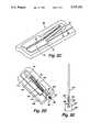
- FIG. 2Cillustrates another embodiment of a tapered launcher 80, which is an alternative to the structure of the tapered launcher 60 of FIG. 2B, for coupling between an image or insular dielectric waveguide 62 and a microstrip transmission line 64.
- the insular film of the top surface of the tapered portion 74is formed by a continuation of the dielectric substrate layer 72 which is bent upward and continued over the surface of the tapered portion 74, as shown.
- the conductive film 70may also simply be continued up to the upper end of the tapered portion 74.
- the structure of the tapered launcher 80is similar to that of the embodiment of FIG.
- the entire microstrip structurecan be mounted in an angle to the dielectric waveguide structure corresponding to the angle of the tapered portion 74 so that the dielectric layer 72 can be continuous without having to be bent.
- a tapered launcher 90interconnecting a dielectric waveguide 92 and a coaxial transmission line connector 94.
- a coaxial transmission linecomprises a center conductor 44 and an outer conductor 40 (see FIG. 1D) which is coupled to the inner conductor 96 and outer conductor 98 of the connector 94.
- This connectoris mounted on a flange 100 such that the outer conductor couples conductively to the flange 100 and the flange 100 is conductively attached to a conductive ground plane 102, as shown.
- the outer conductor 98is conductively connected to ,the conductive plate 102.
- the center conductor 96which functions as a transmission line is disposed along the tapered surface of the insular film 108 on the tapered dielectric waveguide region 106.
- a thin insular film 108is disposed between the center conductor 96 and the surface of the tapered portion 106.
- the tapered portion 106abuts a waveguide dielectric 110, as shown.
- Both the dielectric waveguide 110 and the tapered portion 106are mounted on the conductive plate 102 which forms an image plane. If an insular waveguide is desired, an insular film 112 is disposed between the plate 102 and the waveguide dielectric 110 as well as under the tapered portion 106, as shown.
- 2Eis a diagram illustrating a tapered launcher 120 coupling a dielectric waveguide 122 to a diode mounted on a microstrip circuit 125 with a microstrip transmission line coupling between the diode 124 and the launcher 120.
- a diamond shape conductive waveguide portion 130is utilized for impedance matching in conjunction with the tapered dielectric portion 132, as shown.
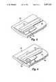
- a distributed signal launcher 150utilizes a coupling region comprising a region in which a dielectric waveguide 152 of high permittivity (e.g., 4 to 100) and a conductive strip transmission line 154 are configured in parallel and in close proximity along a length sufficient to mode convert and couple a signal from one waveguide to the other.
- a microstrip structurecomprises a conductive ground plane 156 covered with a layer of dielectric substrate material 158 of intermediate permittivity (e.g., 2 to 8) on which the conductive strip 154 is mounted.
- An insular waveguidecomprises the conductive ground plane 156 on which the dielectric waveguide 152 is mounted with an insular film 160 disposed there between, as shown.
- the launcher 150comprises a coupling region in which a portion of the dielectric waveguide 152 continues for a predetermined length over the dielectric layer 158 and parallel to the conductive strip transmission line 154.
- the distance between the two waveguides 152, 154 in the coupling regionis preferably less than the width of the conductive strip 154.
- the permittivity of the layer 158be much less (e.g., 2 to 10 times less) than that of the dielectric waveguide 152.
- the thickness of the dielectric layer 158is preferably a conventional value selected to be small enough to suppress horizontal polarization modes in the dielectric waveguide and large enough to obtain acceptable impedance and loss characteristics.
- typical dimensions for a 90 GHz applicationwould be a thickness of the dielectric layer 158 of 0.05-0.20 millimeters, a distance between waveguides 152, 154 of 0.03 millimeters, a width of the conductive strip 154 of 0.05 millimeters, and dimensions of 0.6 millimeters width and 0.5 millimeters height for the dielectric waveguide.
- Typical permittivity valuesmay be 2.25 for the dielectric layer 158 and 10 for the dielectric waveguide 152, while the preferred length of the coupling region is in the range of 3-20 wavelengths.
- FIG. 4is a schematic representation of a crossed waveguide distributed launcher 170 according to the invention for coupling between a high permittivity dielectric waveguide 172 (insular in the illustrated embodiment) and conductive strip transmission line 174.
- the dielectric waveguide 172may include an insular film 176 disposed between the waveguide 172 and a conductive ground plane 178.
- a conductive strip 174fixed to a dielectric substrate layer 180, as shown, to form a microstrip transmission line structure.
- the waveguides 172, 174are configured to cross at a predetermined angle 182 (less than 90°) with the dielectric waveguide 172 crossing over the conductive strip 174, as shown, to form a coupling region in which the two waveguides are in close proximity.
- the dielectric substrate material 180serves as the insular film to support the insular guide 172 in the region of coupling.
- an insular film layer 184may optionally be interposed between the conductive waveguide 174 and the dielectric waveguide 172 to ensure that they do not make direct contact.
- the launcher 170is constructed with the conductive strip 174 made very thin and recessed into the dielectric layer 180 or into the insular guide 172. As an example, a typical angle may be 45° and a permittivity value may be 2.25 for the dielectric layer 180 and 10 for the dielectric waveguide 172.
- a straddled waveguide distributed launcher 190comprising a dielectric waveguide 192 and a conductive strip transmission line 194.
- the dielectric waveguide 192is mounted on the conductive ground plane 196 with an insular film 198 disposed therebetween and extends over a dielectric substrate layer 200 attached to a portion of the ground plane 196, as shown.
- the thin conductive strip 194is fixed to the dielectric layer 200 to form a microstrip structure and is configured such that it is completely straddled by the dielectric waveguide 192 over a predetermined length forming a coupling region.
- This structureis a special case of the crossed waveguide structure of FIG. 4 wherein the crossing angle is 0°.
- An insular layer 202may be disposed between the dielectric waveguide and the conductive waveguide to ensure that they do not come in direct contact. This structure may also be constructed utilizing a thin conductive strip recessed into the dielectric layer 200.
- the materials and dimensionsare selected based on conventional known practice for selecting values for dielectric waveguide and microstrip structures.
- the microstrip dimensions and materialsare chosen to support a single TEM mode of selected nominal constant impedance (e.g., 50 ohms) in the absence of the insular or image waveguide portion.
- the structureis configured to maximize efficient conversion to transfer electromagnetic energy between modes without generating other modes or generating radiation of the electromagnetic energy.
- FIG. 6is an illustration of a balanced mixer circuit 210 including a quadrature (90° phase shift) hybrid coupler composed of two insular waveguides 211, 212 with the image plane and insular film not shown.
- the waveguides 211 and 212 of the quadrature hybridcouple local oscillator and radio frequency (RF) input signals to two beam lead Schottky barrier mixer diodes 214, 216 mounted on a microstrip circuit 220.
- Tapered signal launchers 222, 224are used to couple between the waveguides 211 and 212 and the microstrip diode mounts, as shown.
- the microstrip circuitprovides intermediate frequency (IF) filtering for the mixer diodes 214, 216.
- IFintermediate frequency
- Microstrip circuitincludes such common structures as IF filter elements 226, 228; RF grounding shorts 230, 232; diodes bias inputs 234, 236; coupling capacitors 240, 242; RF choke 246; and IF output 244.
- This mixer circuit 210illustrates the application of the tapered launcher for converting and coupling between an E 11 ⁇ mode dielectric waveguide structure and a TEM mode microstrip structure for purposes of mounting active devices such as beam lead mixer diodes.
- a microstrip to dielectric waveguide signal launcher structure 250which provides abrupt mode conversion and signal coupling.
- the launcher 250comprises a short dielectric waveguide portion 252, having insular film 272 and metal film 266 on three sides, mounted on a ground plane 254 which may include an insular film 256 disposed there between.
- a dielectric waveguide 270continues from the short launcher portion 252.
- the launcher 250comprises a metallic mode shield 266 which forms a narrow metallic sidewall strip on the top and each side of the dielectric waveguide portion 252 at the front face end, as shown.
- a conductive transition flange 268is conductably connected to the top strip of the mode shield 266 and to the microstrip waveguide 262.
- An insular film 272is disposed on the surface of the waveguide portion 252 such that it is interposed between the metal mode shield 266, and the dielectric waveguide portion 252. The insular film may cover the end face of the dielectric waveguide portion 252 as well.
- the sidewall mode shield 266is provided to trap local modes and prevent sidewall radiation. This metallization acts as a shield only for local modes and does not perturb the primary mode (e.g., E 11 ⁇ ) of propagation in the dielectric waveguide because it is on the outer surface of the sidewall insular film.
- the metal strip 266provides efficient coupling to the TEM mode microstrip transmission line.
- FIG. 7Bis an exploded view illustrating an embodiment of the abrupt launcher in which a beam lead diode 280 is mounted on the front wall 258 of a dielectric waveguide portion 294 on a translation flange 282, as shown.
- the dielectric waveguide portion 294is a short section with a length of (n ⁇ /4) where ⁇ is the wavelength and n is a small (i.e., less than 10) odd integer.
- the diode 280is mounted so as to couple signal through it from the transmission line 262 via a translation strip 286 to the dielectric waveguide portion 294.
- a conductive bonding strap 290may be used to ensure conductive coupling between the translation strip (e.g. flange) 286 and the microstrip conductive transmission line 262, as shown.
- a second mode shield 292may optionally be formed at the second end of the dielectric waveguide portion 294 forming narrow metalization on the top and each side of the dielectric portion 294, as well as covering the end face (i.e., back wall, not shown).
- This mode shield 292 together with the mode shield 266forms a stub or cavity which enhances coupling of energy into the diode.
- This structureis highly suitable for mixer and oscillator structures.
- An insular film 272may also be disposed between the surface of the dielectric 294 and the metal mode shields 266, 292.
- a matching stub 288is also shown which provides impedance matching, thereby providing improved launcher efficiency.
Landscapes
- Waveguides (AREA)
Abstract
Description
The present invention relates generally to improvements in high frequency communication systems and particularly to signal launchers for coupling signals to and from dielectric insular and image waveguide transmission lines to TEM mode transmission lines.
Waveguide transmission lines are widely used to channel the flow of high frequency electromagnetic energy. Common transmission lines are coaxial transmission lines, and planar transmission lines such as microstrip transmission lines, and dielectric waveguide transmission lines with ground plane. Dielectric waveguides includes image and insular waveguide transmission lines.
Image and insular waveguide transmission lines exhibit low loss at high frequencies such as in the 10 GHz to 300 GHz frequency range, and are therefore highly suitable for applications at such high frequencies. However, in the prior art, such dielectric waveguides have been difficult to integrate with active devices. Microstrip structures in which the electromagnetic energy propagates in a TEM mode have high loss at such high frequencies, but are highly suitable for integration of active devices. Thus, a high efficiency signal launcher for coupling between dielectric waveguides and microstrip structures, as well as other TEM structures, such as coaxial transmission lines would be advantageous and would facilitate construction of hybrid microwave and millimeter wave circuitry.
It is accordingly an object of the present invention to provide novel apparatus for coupling between dielectric waveguides and TEM waveguide structures such as microstrip and coaxial transmission lines.
It is another object of the present invention to provide novel distributed signal launchers for coupling between dielectric insular or image waveguides and microstrip or coaxial waveguides.
It is yet another object of the invention to provide a novel tapered waveguide signal launcher structure for distributed coupling between a dielectric waveguide and a TEM structure.
It is yet another object of the invention to provide a novel parallel waveguide signal launcher structure for distributed coupling between a dielectric waveguide and a TEM structure.
It is yet another object of the present invention to provide a novel crossed waveguide signal launcher structure for distributed coupling between a dielectric waveguide and a TEM structure.
It is yet another object of the present invention to provide a novel straddled waveguide signal launcher structure for distributed coupling between a dielectric waveguide and a TEM structure.
Briefly, according to one embodiment of the invention, apparatus is provided for a mode conversion signal launcher for coupling signals of a predetermined wavelength between a dielectric waveguide and a TEM mode transmission line. The launcher comprises a conductive ground plane and an elongated high permittivity dielectric waveguide of predetermined cross section adjacent to the conductive ground plane. A TEM mode transmission line is provided having an elongated conducting waveguide portion fixed adjacent to a portion of the dielectric waveguide such that the dielectric waveguide and conductive portions form a distributed coupling region having a length of least two times the predetermined wavelength.
The invention, together with further objects and advantages thereof, may be understood by reference to the following description taken in conjunction with the accompanying drawings.
FIGS. 1A, 1B, 1C, and 1D are illustrations of several prior art waveguide structures.
FIGS. 2A is a schematic representation illustrating a tapered signal launcher according to the invention.
FIGS. 2B is a schematic representation illustrating a tapered signal launcher coupled to a microstrip structure.
FIGS. 2C is a schematic representation illustrating an alternative tapered signal launcher structure coupled to a microstrip structure.
FIGS. 2D is a schematic representation illustrating a tapered signal launcher coupled to a coaxial transmission line.
FIG. 2E is a schematic representation illustrating an alternative shape to the metal conductive waveguide of the tapered launcher of FIG. 2A.
FIG. 3 is a schematic representation illustrating a parallel waveguide structure signal launcher according to the invention.
FIG. 4 is a schematic representation illustrating a crossed waveguide structure signal launcher according to the invention.
FIG. 5 is a schematic representation illustrating a straddled waveguide structure signal launcher according to the invention.
FIG. 6 is a schematic representation illustrating a dielectric waveguide microstrip mixer structure constructed using a tapered signal launcher structure according to the invention.
FIG. 7A is a schematic representation illustrating an abrupt coupling signal launcher coupled to a microstrip structure according to the invention.
FIG. 7B is a detailed blow up of a schematic representation illustrating an alternative abrupt coupling signal launcher coupled to a microstrip structure according to the invention.
FIG. 1A illustrates a prior art dielectricimage waveguide structure 10 comprising a conductive metal ground plane (image plane) in the form of aconductive plate 12. An elongateddielectric waveguide 14 having a rectangular or square cross-section and composed of high permittivity (e.g. 10) dielectric material is mounted in intimate contact with the upper surface of theconductive image plate 12, as shown. A variation of the image dielectric waveguide is the insulardielectric waveguide structure 20 illustrated in FIG. IB. Theinsular waveguide structure 20 comprises a conductive base plate 22 (ground plane) and adielectric waveguide 24 composed of a high permittivity (e.g., 10) dielectric material such as ceramic, alumina, quartz, ceramic filled synthetic organic resin, etc., as in the image waveguide structure. However, there is disposed between theconductive base plate 22 and the dielectric waveguide 24 a thindielectric film 26 of low permittivity (e.g., less than 3) and low loss (e.g., loss tangent less than 0.001) such as a synthetic organic resin, e.g., polyethylene. The film extends laterally beyond the sides of thedielectric waveguide 24 and is intimately connected to both thebase plate 22 and thedielectric waveguide 24. Although thedielectric waveguides
While the above-described dielectric waveguides permit high frequency electromagnetic energy propagation in waveguide electromagnetic field modes such as the E11 ∥ mode, other widely utilized transmission line structures, particularly microstrip and coaxial transmission lines, permit propagation in the Transverse Electro-Magnetic (TEM) mode. FIG. 1C illustrates amicrostrip structure 30 which comprises a conductive ground plane in the form of aconductive metal plate 32 with adielectric layer 34 of various permittivities (e.g., typically 2.5 but as high as 10) affixed to the surface of theconductive plate 32. A conductivethin strip 36, typically metal, is mounted on the surface of thedielectric layer 34, as shown. Resulting structure may be fabricated in an integrated form with active device integrated directly with waveguide structures using the same dielectric and ground plane.
FIG. 1D illustrates a coaxialtransmission line structure 40 which comprises anouter conductor 42 and aninner conductor 44 which is surrounded by the outer conductor. Adielectric material 46 separates the inner conductor and the outer conductor. Both the microstrip structure and the coaxial structure propagate high frequency electromagnetic energy in the TEM mode while thedielectric waveguide structures
While microstrip structures provide the basis for integrating active devices, they suffer from high loss and low Q at high frequencies (i.e., above 10 GHz). Further, microstrip permits the advantage of maintaining the purity of the propagation mode to the very contacts of the active devices in high frequency circuits so that impedance matching can be effectively and reproducible achieved. Conversely, dielectric waveguide structures are difficult to integrate with active devices (i.e., diodes, transistors, etc.) but exhibit much lower loss and higher Q characteristics at high frequencies. By combining these advantages of microstrip to permit integration of active devices and the low loss, high Q characteristics of dielectric waveguides, substantial circuit improvements can be obtained. However, since electromagnetic energy propagates in different modes in the dielectric waveguides than in microstrip waveguides, any interconnection between them requires a mode converting signal launcher.
FIG. 2A illustrates a tapered structure mode convertingsignal launcher 50 which may function, for example, as a launcher for converting E11 ∥ mode to TEM mode. The taperedlauncher 50 converts the E11 ∥ mode to the TEM mode through the interaction of a thinconductive strip 52 on a taperedportion 54 of adielectric waveguide 56 with the fringe fields of the E11 ∥. Thus a coupling region is formed in which thedielectric waveguide 56 is configured adjacent to theconductive strip 52 to provide mode conversion and signal coupling.
The taperedlauncher 50 comprises a taperedportion 54 which tapers towards animage plane 58, which is typically a conductive plate or thin conductive layer. The taperedportion 54 is mated to thedielectric waveguide 56 by a butting connection, or may be integral with thewaveguide 56. In the illustrated embodiment, the taperedportion 54 and thewaveguide 56 may be made, for example, of alumina. The taperedportion 54 preferably has a height and width at one end to permit mating with thedielectric waveguide 56 while the other end has a substantially reduced height, and may have a width the same as that of thedielectric waveguide 56. The height at the low end is selected to provide physical compatibility and impedance matching to the TEM structure to which it is coupled. The length of the taperedportion 54 is also selected to allow gradual conversion of the E11 ∥ mode to the TEM mode and should be at least several times the wavelength in the dielectric waveguide to provide a low VSWR and high coupling efficiency. Typically, a length of 4 to 10 wavelengths is preferred; thus, for example, at 94 GHz, a length of 5 to 15 millimeters will be preferred.
Thedielectric waveguide 56 and the taperedportion 54 may optionally have a thininsular layer 60 of low permittivity material, for example, polyethylene resin, disposed between them and theconductive image plane 58 to form an insular waveguide structure. Aninsular film 62 may also be applied in the preferred embodiment, to the top surface of the taperedportion 54. In the illustrated embodiment, this film preferably has low permittivity (e.g., 2.25) similar to theinsular film 60 between theimage plane 58 and thedielectric waveguide 56.
The thinconductive strip 52 is deposited on top of theinsular film 62, as shown, and may typically have a width of 0.2 to 0.4 millimeters in a 94 GHz application. Theconductive metal strip 52 may also be deposited directly on the tapered surface, and may have a variety of widths and shapes. For example, FIG. 2E illustrates atapered launcher 120 coupling adielectric waveguide 122 to adiode 124 on amicrostrip circuit 125 with a thinconductive strip 130 having a diamond shape. The thin conductive strip of the taperedlauncher structure 50 is connected directly to a thin conductive strip of the desired TEM structure such as a microstrip transmission line or a coaxial transmission line, thereby providing mode converting coupling between the dielectric waveguide and the TEM structure.
As a typical example of suitable dimensions for an E11 ∥/TEM mode launcher using an alumina waveguide to couple to a microstrip structure at 70 GHz, the launcher may typically have a coupling region length of 6 to 10 millimeters, a width of 0.625 millimeters, a height of 0.6 millimeters at the high end, a height of 0.05 millimeters at the low end, and an insular film thickness for both insular films of 0.075 millimeters.
Thelauncher 50 of FIG. 2A may also be used as a mode launcher between other propagation modes and TEM mode. For example, a Quasi-Optical mode waveguide using a larger dimension alumina dielectric waveguide with a cross section of approximately 1.5 millimeters height by 2.5 millimeters width may be used at frequencies in the 100 to 300 GHz range. In such an application, the length of the taperedportion 54 is preferably a larger number of wavelengths in length (i.e., 10 to 50 wavelengths) giving a length of 6 to 30 millimeters. Thin insular layers of 0.025 millimeters may also be preferred for such an application.
In operation, thetapered signal launcher 50 as illustrated in FIG. 2A has exponentially decaying fields (evanescent fields) existing at all surfaces of the waveguide. If any discontinuity is associated with the dielectric/air interface, conversion of the field energy from the E11 ∥ mode to other guided or radiated modes may occur. Thus, in the preferred embodiment, themode launcher 50 is most efficient if theconductor 52 is not in direct contact with the tapered dielectric surface. In the preferred embodiment of thelauncher 50, theconductive strip 52 intercepts only the fringe (evanescent) fields. This minor perturbation of the fringe fields allows the E11 ∥ mode to continue virtually unperturbed. Currents excited in theconductor 52 and theground plane 58 by the fringe fields cause the formation of the field pattern of the TEM mode. Further into the taperedportion 54, the impedance of the E11 ∥ mode decreases and more energy couples into the fringe fields, which causes more coupling into the TEM mode. The conversion is thus highly efficient because there is very little conversion to radiation or to other modes which do not couple to the TEM mode.
Referring now to FIG. 2B, there is shown a schematic representation of a taperedlauncher 60 coupled between a dielectricinsular waveguide 62 and amicrostrip transmission line 64. The dielectric insular waveguide comprises an elongated rectangular cross-sectiondielectric waveguide 62 mounted on an image plane in the form of aconductive plate 66 with aninsular film 68 dispersed therebetween. Themicrostrip transmission line 64 comprises a thinconductive strip 70 mounted on adielectric substrate 72 which is fixed to theconductive plate 66. Theconductive plate 66 may be a single unified conductive plate or separate plates in conductive contact with each other.
The taperedlauncher 60 comprises a tapereddielectric portion 74 mounted on theinsular film 68 which is fixed to theconductive plate 66, as shown. Theinsular film 68 would not be present for an image waveguide structure. In the preferred embodiment, anotherinsular film 78 covers the top surface of the taperedportion 74. The edge of theinsular film 68 and the lower end of the taperedportion 74 abut the edge of thedielectric substrate 72 and theconductive waveguide 70, as shown. Theconductive strip 70 is conductively connected with theconductive strip portion 76 which is mounted on the surface of theinsular film 78, as shown. With this structure, the tapered launcher couples the TEM mode signals from the microstrip transmission line to, for example, a E11 ∥ of the dielectricinsular waveguide 60 or conversely from the dielectricinsular waveguide 60 to the TEM mode of the microstrip transmission line.
FIG. 2C illustrates another embodiment of a taperedlauncher 80, which is an alternative to the structure of the taperedlauncher 60 of FIG. 2B, for coupling between an image or insulardielectric waveguide 62 and amicrostrip transmission line 64. In the embodiment of FIG. 2C, the insular film of the top surface of the taperedportion 74 is formed by a continuation of thedielectric substrate layer 72 which is bent upward and continued over the surface of the taperedportion 74, as shown. Theconductive film 70 may also simply be continued up to the upper end of the taperedportion 74. Thus, the structure of the taperedlauncher 80 is similar to that of the embodiment of FIG. 2B except that thedielectric substrate 72 and theconductive film 70 of the microstrip transmission line structure continue up the taperedportion 74 of the launcher. In the event that anonbendable dielectric layer 72 is used, the entire microstrip structure can be mounted in an angle to the dielectric waveguide structure corresponding to the angle of the taperedportion 74 so that thedielectric layer 72 can be continuous without having to be bent.
Referring to FIG. 2D, there is shown a taperedlauncher 90 interconnecting adielectric waveguide 92 and a coaxialtransmission line connector 94. A coaxial transmission line comprises acenter conductor 44 and an outer conductor 40 (see FIG. 1D) which is coupled to theinner conductor 96 andouter conductor 98 of theconnector 94. This connector is mounted on aflange 100 such that the outer conductor couples conductively to theflange 100 and theflange 100 is conductively attached to aconductive ground plane 102, as shown. As a result, theouter conductor 98 is conductively connected to ,theconductive plate 102. Thecenter conductor 96, which functions as a transmission line is disposed along the tapered surface of theinsular film 108 on the tapereddielectric waveguide region 106. A thininsular film 108 is disposed between thecenter conductor 96 and the surface of the taperedportion 106. The taperedportion 106 abuts awaveguide dielectric 110, as shown. Both thedielectric waveguide 110 and the taperedportion 106 are mounted on theconductive plate 102 which forms an image plane. If an insular waveguide is desired, aninsular film 112 is disposed between theplate 102 and thewaveguide dielectric 110 as well as under the taperedportion 106, as shown. FIG. 2E is a diagram illustrating atapered launcher 120 coupling adielectric waveguide 122 to a diode mounted on amicrostrip circuit 125 with a microstrip transmission line coupling between thediode 124 and thelauncher 120. A diamond shapeconductive waveguide portion 130 is utilized for impedance matching in conjunction with the tapereddielectric portion 132, as shown.
Referring to FIG. 3, there is shown another embodiment of a distributedsignal launcher 150 according to the invention. Thelauncher 150 utilizes a coupling region comprising a region in which adielectric waveguide 152 of high permittivity (e.g., 4 to 100) and a conductivestrip transmission line 154 are configured in parallel and in close proximity along a length sufficient to mode convert and couple a signal from one waveguide to the other. In the illustrated embodiment, a microstrip structure comprises aconductive ground plane 156 covered with a layer ofdielectric substrate material 158 of intermediate permittivity (e.g., 2 to 8) on which theconductive strip 154 is mounted. An insular waveguide comprises theconductive ground plane 156 on which thedielectric waveguide 152 is mounted with aninsular film 160 disposed there between, as shown. Thelauncher 150 comprises a coupling region in which a portion of thedielectric waveguide 152 continues for a predetermined length over thedielectric layer 158 and parallel to the conductivestrip transmission line 154. In the illustrated embodiment, the distance between the twowaveguides conductive strip 154. In addition, it is preferable that the permittivity of thelayer 158 be much less (e.g., 2 to 10 times less) than that of thedielectric waveguide 152. In addition, the thickness of thedielectric layer 158 is preferably a conventional value selected to be small enough to suppress horizontal polarization modes in the dielectric waveguide and large enough to obtain acceptable impedance and loss characteristics. For example, typical dimensions for a 90 GHz application would be a thickness of thedielectric layer 158 of 0.05-0.20 millimeters, a distance betweenwaveguides conductive strip 154 of 0.05 millimeters, and dimensions of 0.6 millimeters width and 0.5 millimeters height for the dielectric waveguide. Typical permittivity values, may be 2.25 for thedielectric layer dielectric waveguide 152, while the preferred length of the coupling region is in the range of 3-20 wavelengths.
FIG. 4 is a schematic representation of a crossed waveguide distributedlauncher 170 according to the invention for coupling between a high permittivity dielectric waveguide 172 (insular in the illustrated embodiment) and conductivestrip transmission line 174. As shown, thedielectric waveguide 172 may include aninsular film 176 disposed between thewaveguide 172 and aconductive ground plane 178. Also mounted on theground plane 178 is aconductive strip 174 fixed to adielectric substrate layer 180, as shown, to form a microstrip transmission line structure. Thewaveguides dielectric waveguide 172 crossing over theconductive strip 174, as shown, to form a coupling region in which the two waveguides are in close proximity. Thedielectric substrate material 180 serves as the insular film to support theinsular guide 172 in the region of coupling. In addition, in the region or intersection of the two waveguides, aninsular film layer 184 may optionally be interposed between theconductive waveguide 174 and thedielectric waveguide 172 to ensure that they do not make direct contact. Thelauncher 170 is constructed with theconductive strip 174 made very thin and recessed into thedielectric layer 180 or into theinsular guide 172. As an example, a typical angle may be 45° and a permittivity value may be 2.25 for thedielectric layer dielectric waveguide 172.
Referring now to FIG. 5, there is shown a straddled waveguide distributedlauncher 190 comprising adielectric waveguide 192 and a conductivestrip transmission line 194. Thedielectric waveguide 192 is mounted on theconductive ground plane 196 with aninsular film 198 disposed therebetween and extends over adielectric substrate layer 200 attached to a portion of theground plane 196, as shown. The thinconductive strip 194 is fixed to thedielectric layer 200 to form a microstrip structure and is configured such that it is completely straddled by thedielectric waveguide 192 over a predetermined length forming a coupling region. This structure is a special case of the crossed waveguide structure of FIG. 4 wherein the crossing angle is 0°. Aninsular layer 202 may be disposed between the dielectric waveguide and the conductive waveguide to ensure that they do not come in direct contact. This structure may also be constructed utilizing a thin conductive strip recessed into thedielectric layer 200.
The construction of various embodiments of the distributed launcher for the present invention, the materials and dimensions are selected based on conventional known practice for selecting values for dielectric waveguide and microstrip structures. Thus, the microstrip dimensions and materials are chosen to support a single TEM mode of selected nominal constant impedance (e.g., 50 ohms) in the absence of the insular or image waveguide portion. The image or insular waveguide dimensions -=nd materials are similarly selected such that, in the absence of the microstrip portions, the dielectric waveguide supports a sired mode such as the E11 ∥ mode and no other higher order E or H modes can exist. In the coupling region, the structure is configured to maximize efficient conversion to transfer electromagnetic energy between modes without generating other modes or generating radiation of the electromagnetic energy.
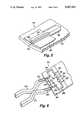
FIG. 6 is an illustration of abalanced mixer circuit 210 including a quadrature (90° phase shift) hybrid coupler composed of twoinsular waveguides waveguides barrier mixer diodes microstrip circuit 220.Tapered signal launchers waveguides mixer diodes filter elements RF grounding shorts inputs coupling capacitors RF choke 246; and IFoutput 244. Thismixer circuit 210 illustrates the application of the tapered launcher for converting and coupling between an E11 ∥ mode dielectric waveguide structure and a TEM mode microstrip structure for purposes of mounting active devices such as beam lead mixer diodes.
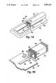
Referring to FIG. 7A, there is shown a microstrip to dielectric waveguidesignal launcher structure 250 which provides abrupt mode conversion and signal coupling. Thelauncher 250 comprises a shortdielectric waveguide portion 252, havinginsular film 272 andmetal film 266 on three sides, mounted on aground plane 254 which may include aninsular film 256 disposed there between. Adielectric waveguide 270 continues from theshort launcher portion 252. Adjacent tofront face 258 of thewaveguide portion 252, amicrostrip transmission line 262 is mounted on ad&electric layer 260 attached to theground plane 254. Thelauncher 250 comprises ametallic mode shield 266 which forms a narrow metallic sidewall strip on the top and each side of thedielectric waveguide portion 252 at the front face end, as shown. Aconductive transition flange 268 is conductably connected to the top strip of themode shield 266 and to themicrostrip waveguide 262. Aninsular film 272 is disposed on the surface of thewaveguide portion 252 such that it is interposed between themetal mode shield 266, and thedielectric waveguide portion 252. The insular film may cover the end face of thedielectric waveguide portion 252 as well.
Thesidewall mode shield 266 is provided to trap local modes and prevent sidewall radiation. This metallization acts as a shield only for local modes and does not perturb the primary mode (e.g., E11 ∥) of propagation in the dielectric waveguide because it is on the outer surface of the sidewall insular film. Themetal strip 266 provides efficient coupling to the TEM mode microstrip transmission line.
FIG. 7B is an exploded view illustrating an embodiment of the abrupt launcher in which abeam lead diode 280 is mounted on thefront wall 258 of adielectric waveguide portion 294 on atranslation flange 282, as shown. Thedielectric waveguide portion 294 is a short section with a length of (n λ/4) where λ is the wavelength and n is a small (i.e., less than 10) odd integer. Thediode 280 is mounted so as to couple signal through it from thetransmission line 262 via atranslation strip 286 to thedielectric waveguide portion 294. Aconductive bonding strap 290 may be used to ensure conductive coupling between the translation strip (e.g. flange) 286 and the microstripconductive transmission line 262, as shown. Asecond mode shield 292 may optionally be formed at the second end of thedielectric waveguide portion 294 forming narrow metalization on the top and each side of thedielectric portion 294, as well as covering the end face (i.e., back wall, not shown). Thismode shield 292 together with themode shield 266 forms a stub or cavity which enhances coupling of energy into the diode. This structure is highly suitable for mixer and oscillator structures. Aninsular film 272 may also be disposed between the surface of the dielectric 294 and the metal mode shields 266, 292. A matchingstub 288 is also shown which provides impedance matching, thereby providing improved launcher efficiency.
Specific embodiments of the signal launcher according to the invention have been described for the purpose of illustrating the manner in which the invention may be made and used. It should be understood that implementation of other variations and modifications of the invention in its various aspects will be apparent to those skilled in the art, and that the invention is not limited by the specific embodiments described. It is therefore contemplated to cover by the present invention any and all modifications, variations, or equivalence that fall within the true spirit and scope of the basic underlying principles disclosed and claimed herein.
Claims (21)
1. A signal launcher for coupling signals of predetermined wavelength between a dielectric waveguide and a TEM mode transmission line comprising:
a conductive ground plane;
an elongated high permittivity dielectric waveguide of predetermined cross section mounted adjacent to the conductive ground plane;
a TEM mode transmission line halving an elongated conductive portion fixed adjacent to a portion of the dielectric waveguide such that the dielectric waveguide and the conductive portion form a distributed coupling region having a length of at least two times the predetermined wavelength; and
a film of low permittivity dielectric material disposed between the dielectric waveguide and the conductive portion in the coupling region.
2. The signal launcher of claim 1 wherein a thin low permittivity film of synthetic organic resin is disposed between and secured to both said conductive ground plane and said dielectric waveguide.
3. The signal launcher of claim 1 wherein the dielectric waveguide in the coupling region is tapered towards said ground plane to form a tapered surface and the conductive portion is fixed adjacent to the top of the tapered surface.
4. The signal launcher of claim 3 wherein the TEM mode transmission line comprises a microstrip transmission line structure comprising an elongated conductive strip fixed to a thin layer of dielectric material which is fixed to the surface of the conductive ground plane and wherein in the coupling region the conductive strip is fixed adjacent to the top of the tapered surface.
5. The signal launcher of claim 1 wherein the dielectric waveguide and the conductive portion are configured in parallel and in close proximity to each other in the coupling region.
6. The signal launcher of claim 1 wherein the dielectric waveguide crosses over the conductive portion at a predetermined angle in the coupling region.
7. The signal launcher of claim 6 wherein the conductive portion is recessed into a layer of dielectric material disposed between the ground plane and the conductive portion.
8. The signal launcher of claim 1 wherein the dielectric waveguide is fixed directly on top and in parallel with the conductive portion in the coupling region.
9. The signal launcher of claim 8 wherein the conductive portion is recessed into a layer of dielectric material disposed between the ground plane and the conductive portion.
10. The signal launcher of claim 1 wherein the TEM mode transmission line comprises a microstrip transmission line structure comprising an elongated conductive strip fixed to a thin layer of dielectric material which is fixed to the surface of the conductive ground plane.
11. The signal launcher of claim 1 wherein the TEM mode transmission line comprises a coaxial transmission line comprising an elongated metallic conductor configured as an inner conductor disposed within an outer conductor and wherein a portion of the inner conductor is fixed adjacent to the dielectric waveguide, said outer conductor having one end thereof secured to the surface of the conductive ground plane.
12. A signal launcher for coupling signals of predetermined nominal wavelength between a dielectric waveguide and a TEM transmission line, comprising:
a conductive ground plane;
a high permittivity dielectric waveguide portion having a front face and a back face mounted adjacent to the conductive ground plane;
a conductive mode shield mounted at the front face of the waveguide portion covering a short portion of the outer surface of the waveguide portion including a conductive flange for coupling to the TEM transmission line; and
a thin low permittivity film of dielectric material disposed between the conductive mode shield and the dielectric waveguide portion surface.
13. The signal launcher of claim 12 wherein a thin low permittivity film of resin is disposed between the conductive ground plane and the dielectric waveguide portion.
14. The signal launcher of claim 12 wherein the conductive flange comprises a top and a bottom conductive flange coupled together by a diode.
15. The signal launcher of claim 12 wherein a second conductive mode shield is mounted at the back face of the waveguide portion covering a narrow portion of the outer surface and covering the back face of the waveguide portion, and wherein the waveguide portion has a length of n λ/4 where λ is the nominal wavelength and n is a small, odd integer.
16. A signal launcher for coupling signals of predetermined wavelength between a dielectric waveguide and a TEM mode transmission line comprising:
a conductive group plane;
an elongated high permittivity dielectric waveguide of predetermined cross section mounted adjacent to the conductive ground plate;
a TEM mode transmission line having an elongated conductive portion fixed adjacent to a portion of the dielectric waveguide such that the dielectric waveguide crosses over the conductive portion at a predetermined angle to form a distributed coupling region having a length of at least two times the predetermined wavelength; and
a thin low permittivity film of synthetic organic resin disposed between and secured to both said conductive ground plane and said dielectric waveguide.
17. The signal launcher of claim 16 wherein a thin film of low permittivity dielectric material is disposed between the dielectric waveguide and the conductive portion in the coupling region where the waveguide and conductive portion cross.
18. The signal launcher of claim 16 wherein the TEM mode transmission line comprises a microstrip transmission line structure comprising an elongated conducive strip fixed to a thin layer of dielectric material which is fixed to the surface of the conductive ground plane.
19. A signal launcher for coupling signals of predetermined wavelength between a dielectric waveguide and a TEM mode transmission line comprising:
a conductive ground plane;
an elongated high permittivity dielectric waveguide of predetermined cross section mounted adjacent to the conductive ground plane;
a TEM mode transmission line having an elongated conductive portion fixed adjacent to a portion of the dielectric waveguide such that the dielectric waveguide and the conductive portion form a distributed coupling region having a length of at least two times the predetermined wavelength wherein a thin film of low permittivity dielectric material is disposed between the dielectric waveguide and conductive portion in the coupling region and wherein the dielectric waveguide is fixed directly on top and in parallel with the conductive portion in the coupling region; and
a thin low permittivity film of synthetic organic resin disposed between and secured to both said conductive ground plane and said dielectric waveguide.
20. A signal launcher for coupling signals of predetermined wavelength between a dielectric waveguide and a TEM mode transmission lines comprising:
a conductive ground plane;
an elongated high permittivity dielectric waveguide of predetermined cross section mounted adjacent to the conductive ground plane;
a TEM mode transmission line having an elongated conductive portion fixed adjacent to a portion of the dielectric waveguide such that the dielectric waveguide crosses over the conductive portion at a predetermined non-zero angle such that the conductive portion is between the dielectric waveguide and the ground plane to form a distributed coupling region having a length of at lest two times the predetermined wavelength.
21. The signal launcher of claim 20 wherein the conductive portion is recessed into a layer of dielectric material disposed between the ground plane and the conductive portion.
Priority Applications (1)
| Application Number | Priority Date | Filing Date | Title |
|---|---|---|---|
| US07/357,345US5107231A (en) | 1989-05-25 | 1989-05-25 | Dielectric waveguide to TEM transmission line signal launcher |
Applications Claiming Priority (1)
| Application Number | Priority Date | Filing Date | Title |
|---|---|---|---|
| US07/357,345US5107231A (en) | 1989-05-25 | 1989-05-25 | Dielectric waveguide to TEM transmission line signal launcher |
Publications (1)
| Publication Number | Publication Date |
|---|---|
| US5107231Atrue US5107231A (en) | 1992-04-21 |
Family
ID=23405218
Family Applications (1)
| Application Number | Title | Priority Date | Filing Date |
|---|---|---|---|
| US07/357,345Expired - Fee RelatedUS5107231A (en) | 1989-05-25 | 1989-05-25 | Dielectric waveguide to TEM transmission line signal launcher |
Country Status (1)
| Country | Link |
|---|---|
| US (1) | US5107231A (en) |
Cited By (182)
| Publication number | Priority date | Publication date | Assignee | Title |
|---|---|---|---|---|
| US5225797A (en)* | 1992-04-27 | 1993-07-06 | Cornell Research Foundation, Inc. | Dielectric waveguide-to-coplanar transmission line transitions |
| US5535296A (en)* | 1994-09-28 | 1996-07-09 | Optobahn Corporation | Integrated optoelectronic coupling and connector |
| US5656980A (en)* | 1994-09-27 | 1997-08-12 | Harris Corporation | Multiple output RF filter and waveguide |
| US20030214364A1 (en)* | 2002-05-16 | 2003-11-20 | Cites Jeffrey S. | Broadband uniplanar coplanar transition |
| US20050128020A1 (en)* | 2001-04-10 | 2005-06-16 | Picosecond Pulse Labs | Ultrafast sampler with non-parallel shockline |
| US20050133922A1 (en)* | 2003-11-12 | 2005-06-23 | Fjelstad Joseph C. | Tapered dielectric and conductor structures and applications thereof |
| US20060244605A1 (en)* | 2005-04-28 | 2006-11-02 | Isao Sakama | Radio frequency identification tag with improved directivity and coverage distance stability |
| US20080012663A1 (en)* | 2006-07-14 | 2008-01-17 | Taiwan Semiconductor Manufacturing Co., Ltd. | Waveguides in integrated circuits |
| US20090091019A1 (en)* | 2003-11-17 | 2009-04-09 | Joseph Charles Fjelstad | Memory Packages Having Stair Step Interconnection Layers |
| US20130126331A1 (en)* | 2011-01-28 | 2013-05-23 | Jozef Kudela | Guided Wave Applicator with Non-Gaseous Dielectric for Plasma Chamber |
| FR3022696A1 (en)* | 2014-06-24 | 2015-12-25 | St Microelectronics Sa | CONNECTOR FOR PLASTIC WAVEGUIDE |
| US20160099749A1 (en)* | 2014-10-03 | 2016-04-07 | At&T Intellectual Property I, Lp | Circuit panel network and methods thereof |
| US9461706B1 (en) | 2015-07-31 | 2016-10-04 | At&T Intellectual Property I, Lp | Method and apparatus for exchanging communication signals |
| US9467870B2 (en) | 2013-11-06 | 2016-10-11 | At&T Intellectual Property I, L.P. | Surface-wave communications and methods thereof |
| US9479266B2 (en) | 2013-12-10 | 2016-10-25 | At&T Intellectual Property I, L.P. | Quasi-optical coupler |
| US9490869B1 (en) | 2015-05-14 | 2016-11-08 | At&T Intellectual Property I, L.P. | Transmission medium having multiple cores and methods for use therewith |
| US9503189B2 (en) | 2014-10-10 | 2016-11-22 | At&T Intellectual Property I, L.P. | Method and apparatus for arranging communication sessions in a communication system |
| US9509415B1 (en) | 2015-06-25 | 2016-11-29 | At&T Intellectual Property I, L.P. | Methods and apparatus for inducing a fundamental wave mode on a transmission medium |
| US9520945B2 (en) | 2014-10-21 | 2016-12-13 | At&T Intellectual Property I, L.P. | Apparatus for providing communication services and methods thereof |
| US9525524B2 (en) | 2013-05-31 | 2016-12-20 | At&T Intellectual Property I, L.P. | Remote distributed antenna system |
| US9525210B2 (en) | 2014-10-21 | 2016-12-20 | At&T Intellectual Property I, L.P. | Guided-wave transmission device with non-fundamental mode propagation and methods for use therewith |
| US9531427B2 (en) | 2014-11-20 | 2016-12-27 | At&T Intellectual Property I, L.P. | Transmission device with mode division multiplexing and methods for use therewith |
| US9571209B2 (en) | 2014-10-21 | 2017-02-14 | At&T Intellectual Property I, L.P. | Transmission device with impairment compensation and methods for use therewith |
| US9577306B2 (en) | 2014-10-21 | 2017-02-21 | At&T Intellectual Property I, L.P. | Guided-wave transmission device and methods for use therewith |
| US9608740B2 (en) | 2015-07-15 | 2017-03-28 | At&T Intellectual Property I, L.P. | Method and apparatus for launching a wave mode that mitigates interference |
| US9608692B2 (en) | 2015-06-11 | 2017-03-28 | At&T Intellectual Property I, L.P. | Repeater and methods for use therewith |
| US9615269B2 (en) | 2014-10-02 | 2017-04-04 | At&T Intellectual Property I, L.P. | Method and apparatus that provides fault tolerance in a communication network |
| US9628854B2 (en) | 2014-09-29 | 2017-04-18 | At&T Intellectual Property I, L.P. | Method and apparatus for distributing content in a communication network |
| US9628116B2 (en) | 2015-07-14 | 2017-04-18 | At&T Intellectual Property I, L.P. | Apparatus and methods for transmitting wireless signals |
| US9640850B2 (en) | 2015-06-25 | 2017-05-02 | At&T Intellectual Property I, L.P. | Methods and apparatus for inducing a non-fundamental wave mode on a transmission medium |
| US9654173B2 (en) | 2014-11-20 | 2017-05-16 | At&T Intellectual Property I, L.P. | Apparatus for powering a communication device and methods thereof |
| US9653770B2 (en) | 2014-10-21 | 2017-05-16 | At&T Intellectual Property I, L.P. | Guided wave coupler, coupling module and methods for use therewith |
| US9667317B2 (en) | 2015-06-15 | 2017-05-30 | At&T Intellectual Property I, L.P. | Method and apparatus for providing security using network traffic adjustments |
| US9680670B2 (en) | 2014-11-20 | 2017-06-13 | At&T Intellectual Property I, L.P. | Transmission device with channel equalization and control and methods for use therewith |
| US9692102B2 (en)* | 2015-09-25 | 2017-06-27 | Texas Instruments Incorporated | Dielectric waveguide socket for connecting a dielectric waveguide stub to a dielectric waveguide |
| US9692101B2 (en) | 2014-08-26 | 2017-06-27 | At&T Intellectual Property I, L.P. | Guided wave couplers for coupling electromagnetic waves between a waveguide surface and a surface of a wire |
| US9699785B2 (en) | 2012-12-05 | 2017-07-04 | At&T Intellectual Property I, L.P. | Backhaul link for distributed antenna system |
| US9705571B2 (en) | 2015-09-16 | 2017-07-11 | At&T Intellectual Property I, L.P. | Method and apparatus for use with a radio distributed antenna system |
| US9705561B2 (en) | 2015-04-24 | 2017-07-11 | At&T Intellectual Property I, L.P. | Directional coupling device and methods for use therewith |
| US9722318B2 (en) | 2015-07-14 | 2017-08-01 | At&T Intellectual Property I, L.P. | Method and apparatus for coupling an antenna to a device |
| US9729197B2 (en) | 2015-10-01 | 2017-08-08 | At&T Intellectual Property I, L.P. | Method and apparatus for communicating network management traffic over a network |
| US9735833B2 (en) | 2015-07-31 | 2017-08-15 | At&T Intellectual Property I, L.P. | Method and apparatus for communications management in a neighborhood network |
| US9742462B2 (en) | 2014-12-04 | 2017-08-22 | At&T Intellectual Property I, L.P. | Transmission medium and communication interfaces and methods for use therewith |
| US9749053B2 (en) | 2015-07-23 | 2017-08-29 | At&T Intellectual Property I, L.P. | Node device, repeater and methods for use therewith |
| US9748626B2 (en) | 2015-05-14 | 2017-08-29 | At&T Intellectual Property I, L.P. | Plurality of cables having different cross-sectional shapes which are bundled together to form a transmission medium |
| US9749013B2 (en) | 2015-03-17 | 2017-08-29 | At&T Intellectual Property I, L.P. | Method and apparatus for reducing attenuation of electromagnetic waves guided by a transmission medium |
| US9755697B2 (en) | 2014-09-15 | 2017-09-05 | At&T Intellectual Property I, L.P. | Method and apparatus for sensing a condition in a transmission medium of electromagnetic waves |
| US9769128B2 (en) | 2015-09-28 | 2017-09-19 | At&T Intellectual Property I, L.P. | Method and apparatus for encryption of communications over a network |
| US9769020B2 (en) | 2014-10-21 | 2017-09-19 | At&T Intellectual Property I, L.P. | Method and apparatus for responding to events affecting communications in a communication network |
| US9780834B2 (en) | 2014-10-21 | 2017-10-03 | At&T Intellectual Property I, L.P. | Method and apparatus for transmitting electromagnetic waves |
| US9793954B2 (en) | 2015-04-28 | 2017-10-17 | At&T Intellectual Property I, L.P. | Magnetic coupling device and methods for use therewith |
| US9793951B2 (en) | 2015-07-15 | 2017-10-17 | At&T Intellectual Property I, L.P. | Method and apparatus for launching a wave mode that mitigates interference |
| US9793955B2 (en) | 2015-04-24 | 2017-10-17 | At&T Intellectual Property I, Lp | Passive electrical coupling device and methods for use therewith |
| US9800327B2 (en) | 2014-11-20 | 2017-10-24 | At&T Intellectual Property I, L.P. | Apparatus for controlling operations of a communication device and methods thereof |
| US9820146B2 (en) | 2015-06-12 | 2017-11-14 | At&T Intellectual Property I, L.P. | Method and apparatus for authentication and identity management of communicating devices |
| US9838896B1 (en) | 2016-12-09 | 2017-12-05 | At&T Intellectual Property I, L.P. | Method and apparatus for assessing network coverage |
| US9836957B2 (en) | 2015-07-14 | 2017-12-05 | At&T Intellectual Property I, L.P. | Method and apparatus for communicating with premises equipment |
| US9847566B2 (en) | 2015-07-14 | 2017-12-19 | At&T Intellectual Property I, L.P. | Method and apparatus for adjusting a field of a signal to mitigate interference |
| US9847850B2 (en) | 2014-10-14 | 2017-12-19 | At&T Intellectual Property I, L.P. | Method and apparatus for adjusting a mode of communication in a communication network |
| US9853342B2 (en) | 2015-07-14 | 2017-12-26 | At&T Intellectual Property I, L.P. | Dielectric transmission medium connector and methods for use therewith |
| US9860075B1 (en) | 2016-08-26 | 2018-01-02 | At&T Intellectual Property I, L.P. | Method and communication node for broadband distribution |
| US9866309B2 (en) | 2015-06-03 | 2018-01-09 | At&T Intellectual Property I, Lp | Host node device and methods for use therewith |
| US9865911B2 (en) | 2015-06-25 | 2018-01-09 | At&T Intellectual Property I, L.P. | Waveguide system for slot radiating first electromagnetic waves that are combined into a non-fundamental wave mode second electromagnetic wave on a transmission medium |
| US9871283B2 (en) | 2015-07-23 | 2018-01-16 | At&T Intellectual Property I, Lp | Transmission medium having a dielectric core comprised of plural members connected by a ball and socket configuration |
| US9871282B2 (en) | 2015-05-14 | 2018-01-16 | At&T Intellectual Property I, L.P. | At least one transmission medium having a dielectric surface that is covered at least in part by a second dielectric |
| US9876264B2 (en) | 2015-10-02 | 2018-01-23 | At&T Intellectual Property I, Lp | Communication system, guided wave switch and methods for use therewith |
| US9876605B1 (en) | 2016-10-21 | 2018-01-23 | At&T Intellectual Property I, L.P. | Launcher and coupling system to support desired guided wave mode |
| US9876571B2 (en) | 2015-02-20 | 2018-01-23 | At&T Intellectual Property I, Lp | Guided-wave transmission device with non-fundamental mode propagation and methods for use therewith |
| US9882257B2 (en) | 2015-07-14 | 2018-01-30 | At&T Intellectual Property I, L.P. | Method and apparatus for launching a wave mode that mitigates interference |
| US9882277B2 (en) | 2015-10-02 | 2018-01-30 | At&T Intellectual Property I, Lp | Communication device and antenna assembly with actuated gimbal mount |
| US9893795B1 (en) | 2016-12-07 | 2018-02-13 | At&T Intellectual Property I, Lp | Method and repeater for broadband distribution |
| US9904535B2 (en) | 2015-09-14 | 2018-02-27 | At&T Intellectual Property I, L.P. | Method and apparatus for distributing software |
| US9906269B2 (en) | 2014-09-17 | 2018-02-27 | At&T Intellectual Property I, L.P. | Monitoring and mitigating conditions in a communication network |
| US9913139B2 (en) | 2015-06-09 | 2018-03-06 | At&T Intellectual Property I, L.P. | Signal fingerprinting for authentication of communicating devices |
| US9912027B2 (en) | 2015-07-23 | 2018-03-06 | At&T Intellectual Property I, L.P. | Method and apparatus for exchanging communication signals |
| US9912382B2 (en) | 2015-06-03 | 2018-03-06 | At&T Intellectual Property I, Lp | Network termination and methods for use therewith |
| US9912419B1 (en) | 2016-08-24 | 2018-03-06 | At&T Intellectual Property I, L.P. | Method and apparatus for managing a fault in a distributed antenna system |
| US9911020B1 (en) | 2016-12-08 | 2018-03-06 | At&T Intellectual Property I, L.P. | Method and apparatus for tracking via a radio frequency identification device |
| US9917341B2 (en) | 2015-05-27 | 2018-03-13 | At&T Intellectual Property I, L.P. | Apparatus and method for launching electromagnetic waves and for modifying radial dimensions of the propagating electromagnetic waves |
| US9927517B1 (en) | 2016-12-06 | 2018-03-27 | At&T Intellectual Property I, L.P. | Apparatus and methods for sensing rainfall |
| US9948354B2 (en) | 2015-04-28 | 2018-04-17 | At&T Intellectual Property I, L.P. | Magnetic coupling device with reflective plate and methods for use therewith |
| US9948333B2 (en) | 2015-07-23 | 2018-04-17 | At&T Intellectual Property I, L.P. | Method and apparatus for wireless communications to mitigate interference |
| US9954287B2 (en) | 2014-11-20 | 2018-04-24 | At&T Intellectual Property I, L.P. | Apparatus for converting wireless signals and electromagnetic waves and methods thereof |
| US9967173B2 (en) | 2015-07-31 | 2018-05-08 | At&T Intellectual Property I, L.P. | Method and apparatus for authentication and identity management of communicating devices |
| US9973940B1 (en) | 2017-02-27 | 2018-05-15 | At&T Intellectual Property I, L.P. | Apparatus and methods for dynamic impedance matching of a guided wave launcher |
| US9991580B2 (en) | 2016-10-21 | 2018-06-05 | At&T Intellectual Property I, L.P. | Launcher and coupling system for guided wave mode cancellation |
| US9998870B1 (en) | 2016-12-08 | 2018-06-12 | At&T Intellectual Property I, L.P. | Method and apparatus for proximity sensing |
| US9997819B2 (en) | 2015-06-09 | 2018-06-12 | At&T Intellectual Property I, L.P. | Transmission medium and method for facilitating propagation of electromagnetic waves via a core |
| US9999038B2 (en) | 2013-05-31 | 2018-06-12 | At&T Intellectual Property I, L.P. | Remote distributed antenna system |
| US10009063B2 (en) | 2015-09-16 | 2018-06-26 | At&T Intellectual Property I, L.P. | Method and apparatus for use with a radio distributed antenna system having an out-of-band reference signal |
| US10009065B2 (en) | 2012-12-05 | 2018-06-26 | At&T Intellectual Property I, L.P. | Backhaul link for distributed antenna system |
| US10009901B2 (en) | 2015-09-16 | 2018-06-26 | At&T Intellectual Property I, L.P. | Method, apparatus, and computer-readable storage medium for managing utilization of wireless resources between base stations |
| US10009067B2 (en) | 2014-12-04 | 2018-06-26 | At&T Intellectual Property I, L.P. | Method and apparatus for configuring a communication interface |
| US10020844B2 (en) | 2016-12-06 | 2018-07-10 | T&T Intellectual Property I, L.P. | Method and apparatus for broadcast communication via guided waves |
| US10020587B2 (en) | 2015-07-31 | 2018-07-10 | At&T Intellectual Property I, L.P. | Radial antenna and methods for use therewith |
| US10027397B2 (en) | 2016-12-07 | 2018-07-17 | At&T Intellectual Property I, L.P. | Distributed antenna system and methods for use therewith |
| US10033107B2 (en) | 2015-07-14 | 2018-07-24 | At&T Intellectual Property I, L.P. | Method and apparatus for coupling an antenna to a device |
| US10033108B2 (en) | 2015-07-14 | 2018-07-24 | At&T Intellectual Property I, L.P. | Apparatus and methods for generating an electromagnetic wave having a wave mode that mitigates interference |
| US10044409B2 (en) | 2015-07-14 | 2018-08-07 | At&T Intellectual Property I, L.P. | Transmission medium and methods for use therewith |
| US10051483B2 (en) | 2015-10-16 | 2018-08-14 | At&T Intellectual Property I, L.P. | Method and apparatus for directing wireless signals |
| US10051629B2 (en) | 2015-09-16 | 2018-08-14 | At&T Intellectual Property I, L.P. | Method and apparatus for use with a radio distributed antenna system having an in-band reference signal |
| US10069535B2 (en) | 2016-12-08 | 2018-09-04 | At&T Intellectual Property I, L.P. | Apparatus and methods for launching electromagnetic waves having a certain electric field structure |
| US10074890B2 (en) | 2015-10-02 | 2018-09-11 | At&T Intellectual Property I, L.P. | Communication device and antenna with integrated light assembly |
| US10079661B2 (en) | 2015-09-16 | 2018-09-18 | At&T Intellectual Property I, L.P. | Method and apparatus for use with a radio distributed antenna system having a clock reference |
| US10090594B2 (en) | 2016-11-23 | 2018-10-02 | At&T Intellectual Property I, L.P. | Antenna system having structural configurations for assembly |
| US10090606B2 (en) | 2015-07-15 | 2018-10-02 | At&T Intellectual Property I, L.P. | Antenna system with dielectric array and methods for use therewith |
| US10103422B2 (en) | 2016-12-08 | 2018-10-16 | At&T Intellectual Property I, L.P. | Method and apparatus for mounting network devices |
| US10103801B2 (en) | 2015-06-03 | 2018-10-16 | At&T Intellectual Property I, L.P. | Host node device and methods for use therewith |
| US10135145B2 (en) | 2016-12-06 | 2018-11-20 | At&T Intellectual Property I, L.P. | Apparatus and methods for generating an electromagnetic wave along a transmission medium |
| US10135147B2 (en) | 2016-10-18 | 2018-11-20 | At&T Intellectual Property I, L.P. | Apparatus and methods for launching guided waves via an antenna |
| US10136434B2 (en) | 2015-09-16 | 2018-11-20 | At&T Intellectual Property I, L.P. | Method and apparatus for use with a radio distributed antenna system having an ultra-wideband control channel |
| US10135146B2 (en) | 2016-10-18 | 2018-11-20 | At&T Intellectual Property I, L.P. | Apparatus and methods for launching guided waves via circuits |
| US10142086B2 (en) | 2015-06-11 | 2018-11-27 | At&T Intellectual Property I, L.P. | Repeater and methods for use therewith |
| US10139820B2 (en) | 2016-12-07 | 2018-11-27 | At&T Intellectual Property I, L.P. | Method and apparatus for deploying equipment of a communication system |
| US10144036B2 (en) | 2015-01-30 | 2018-12-04 | At&T Intellectual Property I, L.P. | Method and apparatus for mitigating interference affecting a propagation of electromagnetic waves guided by a transmission medium |
| US10148016B2 (en) | 2015-07-14 | 2018-12-04 | At&T Intellectual Property I, L.P. | Apparatus and methods for communicating utilizing an antenna array |
| US10154493B2 (en) | 2015-06-03 | 2018-12-11 | At&T Intellectual Property I, L.P. | Network termination and methods for use therewith |
| US10170840B2 (en) | 2015-07-14 | 2019-01-01 | At&T Intellectual Property I, L.P. | Apparatus and methods for sending or receiving electromagnetic signals |
| US10168695B2 (en) | 2016-12-07 | 2019-01-01 | At&T Intellectual Property I, L.P. | Method and apparatus for controlling an unmanned aircraft |
| US10178445B2 (en) | 2016-11-23 | 2019-01-08 | At&T Intellectual Property I, L.P. | Methods, devices, and systems for load balancing between a plurality of waveguides |
| US10205655B2 (en) | 2015-07-14 | 2019-02-12 | At&T Intellectual Property I, L.P. | Apparatus and methods for communicating utilizing an antenna array and multiple communication paths |
| WO2019040377A1 (en)* | 2017-08-21 | 2019-02-28 | Texas Instruments Incorporated | Launch structures for a hermetically sealed cavity |
| US10225025B2 (en) | 2016-11-03 | 2019-03-05 | At&T Intellectual Property I, L.P. | Method and apparatus for detecting a fault in a communication system |
| US10224634B2 (en) | 2016-11-03 | 2019-03-05 | At&T Intellectual Property I, L.P. | Methods and apparatus for adjusting an operational characteristic of an antenna |
| CN109470397A (en)* | 2017-09-07 | 2019-03-15 | 德克萨斯仪器股份有限公司 | The pressure measurement of electromagnetic signal output based on chamber |
| US10243784B2 (en) | 2014-11-20 | 2019-03-26 | At&T Intellectual Property I, L.P. | System for generating topology information and methods thereof |
| US10243270B2 (en) | 2016-12-07 | 2019-03-26 | At&T Intellectual Property I, L.P. | Beam adaptive multi-feed dielectric antenna system and methods for use therewith |
| US10264586B2 (en) | 2016-12-09 | 2019-04-16 | At&T Mobility Ii Llc | Cloud-based packet controller and methods for use therewith |
| US10291334B2 (en) | 2016-11-03 | 2019-05-14 | At&T Intellectual Property I, L.P. | System for detecting a fault in a communication system |
| US10291311B2 (en) | 2016-09-09 | 2019-05-14 | At&T Intellectual Property I, L.P. | Method and apparatus for mitigating a fault in a distributed antenna system |
| US10298293B2 (en) | 2017-03-13 | 2019-05-21 | At&T Intellectual Property I, L.P. | Apparatus of communication utilizing wireless network devices |
| US10305190B2 (en) | 2016-12-01 | 2019-05-28 | At&T Intellectual Property I, L.P. | Reflecting dielectric antenna system and methods for use therewith |
| US10312567B2 (en) | 2016-10-26 | 2019-06-04 | At&T Intellectual Property I, L.P. | Launcher with planar strip antenna and methods for use therewith |
| US10320586B2 (en) | 2015-07-14 | 2019-06-11 | At&T Intellectual Property I, L.P. | Apparatus and methods for generating non-interfering electromagnetic waves on an insulated transmission medium |
| US10326689B2 (en) | 2016-12-08 | 2019-06-18 | At&T Intellectual Property I, L.P. | Method and system for providing alternative communication paths |
| US10326494B2 (en) | 2016-12-06 | 2019-06-18 | At&T Intellectual Property I, L.P. | Apparatus for measurement de-embedding and methods for use therewith |
| US10340601B2 (en) | 2016-11-23 | 2019-07-02 | At&T Intellectual Property I, L.P. | Multi-antenna system and methods for use therewith |
| US10340600B2 (en) | 2016-10-18 | 2019-07-02 | At&T Intellectual Property I, L.P. | Apparatus and methods for launching guided waves via plural waveguide systems |
| US10340983B2 (en) | 2016-12-09 | 2019-07-02 | At&T Intellectual Property I, L.P. | Method and apparatus for surveying remote sites via guided wave communications |
| US10340573B2 (en) | 2016-10-26 | 2019-07-02 | At&T Intellectual Property I, L.P. | Launcher with cylindrical coupling device and methods for use therewith |
| US10340603B2 (en) | 2016-11-23 | 2019-07-02 | At&T Intellectual Property I, L.P. | Antenna system having shielded structural configurations for assembly |
| US10341142B2 (en) | 2015-07-14 | 2019-07-02 | At&T Intellectual Property I, L.P. | Apparatus and methods for generating non-interfering electromagnetic waves on an uninsulated conductor |
| US10348391B2 (en) | 2015-06-03 | 2019-07-09 | At&T Intellectual Property I, L.P. | Client node device with frequency conversion and methods for use therewith |
| US10355367B2 (en) | 2015-10-16 | 2019-07-16 | At&T Intellectual Property I, L.P. | Antenna structure for exchanging wireless signals |
| US10361489B2 (en) | 2016-12-01 | 2019-07-23 | At&T Intellectual Property I, L.P. | Dielectric dish antenna system and methods for use therewith |
| US10359749B2 (en) | 2016-12-07 | 2019-07-23 | At&T Intellectual Property I, L.P. | Method and apparatus for utilities management via guided wave communication |
| US10374316B2 (en) | 2016-10-21 | 2019-08-06 | At&T Intellectual Property I, L.P. | System and dielectric antenna with non-uniform dielectric |
| US10382976B2 (en) | 2016-12-06 | 2019-08-13 | At&T Intellectual Property I, L.P. | Method and apparatus for managing wireless communications based on communication paths and network device positions |
| US10389029B2 (en) | 2016-12-07 | 2019-08-20 | At&T Intellectual Property I, L.P. | Multi-feed dielectric antenna system with core selection and methods for use therewith |
| US10389037B2 (en) | 2016-12-08 | 2019-08-20 | At&T Intellectual Property I, L.P. | Apparatus and methods for selecting sections of an antenna array and use therewith |
| US10396887B2 (en) | 2015-06-03 | 2019-08-27 | At&T Intellectual Property I, L.P. | Client node device and methods for use therewith |
| US10411356B2 (en) | 2016-12-08 | 2019-09-10 | At&T Intellectual Property I, L.P. | Apparatus and methods for selectively targeting communication devices with an antenna array |
| US10424523B2 (en) | 2017-09-07 | 2019-09-24 | Texas Instruments Incorporated | Hermetically sealed molecular spectroscopy cell with buried ground plane |
| US10439675B2 (en) | 2016-12-06 | 2019-10-08 | At&T Intellectual Property I, L.P. | Method and apparatus for repeating guided wave communication signals |
| US10446936B2 (en) | 2016-12-07 | 2019-10-15 | At&T Intellectual Property I, L.P. | Multi-feed dielectric antenna system and methods for use therewith |
| US10493722B2 (en) | 2017-09-07 | 2019-12-03 | Texas Instruments Incorporated | Hermetically sealed molecular spectroscopy cell with dual wafer bonding |
| US10498044B2 (en) | 2016-11-03 | 2019-12-03 | At&T Intellectual Property I, L.P. | Apparatus for configuring a surface of an antenna |
| US10530505B2 (en) | 2016-12-08 | 2020-01-07 | At&T Intellectual Property I, L.P. | Apparatus and methods for launching electromagnetic waves along a transmission medium |
| US10535928B2 (en) | 2016-11-23 | 2020-01-14 | At&T Intellectual Property I, L.P. | Antenna system and methods for use therewith |
| US10547348B2 (en) | 2016-12-07 | 2020-01-28 | At&T Intellectual Property I, L.P. | Method and apparatus for switching transmission mediums in a communication system |
| US10544039B2 (en) | 2017-09-08 | 2020-01-28 | Texas Instruments Incorporated | Methods for depositing a measured amount of a species in a sealed cavity |
| US10551265B2 (en) | 2017-09-07 | 2020-02-04 | Texas Instruments Incorporated | Pressure sensing using quantum molecular rotational state transitions |
| US10549986B2 (en) | 2017-09-07 | 2020-02-04 | Texas Instruments Incorporated | Hermetically sealed molecular spectroscopy cell |
| US10589986B2 (en) | 2017-09-06 | 2020-03-17 | Texas Instruments Incorporated | Packaging a sealed cavity in an electronic device |
| US10601494B2 (en) | 2016-12-08 | 2020-03-24 | At&T Intellectual Property I, L.P. | Dual-band communication device and method for use therewith |
| US10637149B2 (en) | 2016-12-06 | 2020-04-28 | At&T Intellectual Property I, L.P. | Injection molded dielectric antenna and methods for use therewith |
| US10650940B2 (en) | 2015-05-15 | 2020-05-12 | At&T Intellectual Property I, L.P. | Transmission medium having a conductive material and methods for use therewith |
| US10665942B2 (en) | 2015-10-16 | 2020-05-26 | At&T Intellectual Property I, L.P. | Method and apparatus for adjusting wireless communications |
| US10679767B2 (en) | 2015-05-15 | 2020-06-09 | At&T Intellectual Property I, L.P. | Transmission medium having a conductive material and methods for use therewith |
| US10694379B2 (en) | 2016-12-06 | 2020-06-23 | At&T Intellectual Property I, L.P. | Waveguide system with device-based authentication and methods for use therewith |
| US10727599B2 (en) | 2016-12-06 | 2020-07-28 | At&T Intellectual Property I, L.P. | Launcher with slot antenna and methods for use therewith |
| US10755542B2 (en) | 2016-12-06 | 2020-08-25 | At&T Intellectual Property I, L.P. | Method and apparatus for surveillance via guided wave communication |
| US10777873B2 (en) | 2016-12-08 | 2020-09-15 | At&T Intellectual Property I, L.P. | Method and apparatus for mounting network devices |
| US10775422B2 (en) | 2017-09-05 | 2020-09-15 | Texas Instruments Incorporated | Molecular spectroscopy cell with resonant cavity |
| US10784670B2 (en) | 2015-07-23 | 2020-09-22 | At&T Intellectual Property I, L.P. | Antenna support for aligning an antenna |
| US10811767B2 (en) | 2016-10-21 | 2020-10-20 | At&T Intellectual Property I, L.P. | System and dielectric antenna with convex dielectric radome |
| US10819035B2 (en) | 2016-12-06 | 2020-10-27 | At&T Intellectual Property I, L.P. | Launcher with helical antenna and methods for use therewith |
| US10916969B2 (en) | 2016-12-08 | 2021-02-09 | At&T Intellectual Property I, L.P. | Method and apparatus for providing power using an inductive coupling |
| US10938108B2 (en) | 2016-12-08 | 2021-03-02 | At&T Intellectual Property I, L.P. | Frequency selective multi-feed dielectric antenna system and methods for use therewith |
| US11032819B2 (en) | 2016-09-15 | 2021-06-08 | At&T Intellectual Property I, L.P. | Method and apparatus for use with a radio distributed antenna system having a control channel reference signal |
| US11108433B2 (en)* | 2018-11-30 | 2021-08-31 | Intel Corporation | Single side band transmission over a waveguide |
| US12368111B2 (en)* | 2017-12-22 | 2025-07-22 | Infineon Technologies Ag | Semiconductor apparatuses with radio-frequency line elements, and associated manufacturing methods |
Citations (32)
| Publication number | Priority date | Publication date | Assignee | Title |
|---|---|---|---|---|
| US2901709A (en)* | 1954-12-14 | 1959-08-25 | Gen Electric | Wave coupling arrangement |
| US2976499A (en)* | 1958-05-14 | 1961-03-21 | Sperry Rand Corp | Waveguide to strip transmission line directional coupler |
| US3558213A (en)* | 1969-04-25 | 1971-01-26 | Bell Telephone Labor Inc | Optical frequency filters using disc cavity |
| US3990026A (en)* | 1971-08-02 | 1976-11-02 | National Research Development Corporation | Waveguides |
| US3995238A (en)* | 1975-06-30 | 1976-11-30 | Epsilon Lambda Electronics Corporation | Image waveguide transmission line and mode launchers utilizing same |
| US4034377A (en)* | 1976-02-17 | 1977-07-05 | Epsilon Lambda Electronics Corporation | Ferrite circulators and isolators and circuits incorporating the same |
| US4048589A (en)* | 1975-06-30 | 1977-09-13 | Epsilon Lambda Electronics Corporation | Receiver module and components thereof |
| US4072902A (en)* | 1975-06-30 | 1978-02-07 | Epsilon Lambda Electronics Corp. | Receiver module and mixer thereof |
| US4091343A (en)* | 1975-06-30 | 1978-05-23 | Epsilon Lambda Electronics Corp. | Insular waveguide directional coupler |
| US4097826A (en)* | 1975-06-30 | 1978-06-27 | Epsilon Lambda Electronics Corp. | Insular waveguide ring resonator filter |
| US4215313A (en)* | 1979-05-31 | 1980-07-29 | Hughes Aircraft Company | Dielectric image guide integrated harmonic pumped mixer |
| US4222014A (en)* | 1978-12-26 | 1980-09-09 | Alpha Industries, Inc. | Microwave/millimeterwave oscillator using transferred electron device |
| US4232401A (en)* | 1979-08-20 | 1980-11-04 | The United States Of America As Represented By The Secretary Of The Army | Millimeter wave image guide integrated balanced mixer |
| US4259647A (en)* | 1979-08-20 | 1981-03-31 | The United States Of America As Represented By The Secretary Of The Army | Millimeter wave image guide integrated oscillator |
| US4415871A (en)* | 1981-10-13 | 1983-11-15 | The United States Of America As Represented By The Secretary Of The Army | Dielectric waveguide circulator |
| US4426628A (en)* | 1981-03-23 | 1984-01-17 | The United States Of America As Represented By The Secretary Of The Army | Millimeter wave oscillator with enhanced dielectric coupler |
| US4434409A (en)* | 1981-06-11 | 1984-02-28 | Raytheon Company | Dielectric waveguide phase shifter |
| US4457464A (en)* | 1981-01-13 | 1984-07-03 | Thomson-Csf | Method of fixing a ferrite to a metal piece |
| US4459567A (en)* | 1982-06-14 | 1984-07-10 | The United States Of America As Represented By The Secretary Of The Army | Dielectric waveguide ferrite resonance isolator |
| US4463330A (en)* | 1982-06-09 | 1984-07-31 | Seki & Company, Ltd. | Dielectric waveguide |
| US4502023A (en)* | 1981-06-19 | 1985-02-26 | Thomson-Csf | Method of fabricating a varactor/oscillator diode module for a tunable oscillator |
| US4507664A (en)* | 1981-06-16 | 1985-03-26 | The Secretary Of State For Defence In Her Britannic Majesty's Government Of The United Kingdom Of Great Britain And Northern Ireland | Dielectric image waveguide antenna array |
| US4547901A (en)* | 1982-11-30 | 1985-10-15 | Tokyo Shibaura Denki Kabushiki Kaisha | Microwave receiving apparatus using a waveguide filter |
| US4556855A (en)* | 1983-10-31 | 1985-12-03 | The United States Of America As Represented By The Secretary Of The Navy | RF Components and networks in shaped dielectrics |
| JPS6177403A (en)* | 1984-09-22 | 1986-04-21 | Sumitomo Electric Ind Ltd | Stripline-waveguide converter |
| US4654609A (en)* | 1985-02-25 | 1987-03-31 | The United States Of America As Represented By The Secretary Of The Army | Monolithic planar doped barrier limiter |
| US4673897A (en)* | 1982-04-26 | 1987-06-16 | U.S. Philips Corporation | Waveguide/microstrip mode transducer |
| US4673946A (en)* | 1985-12-16 | 1987-06-16 | Electromagnetic Sciences, Inc. | Ridged waveguide to rectangular waveguide adaptor useful for feeding phased array antenna |
| US4689585A (en)* | 1984-12-19 | 1987-08-25 | Martin Marietta Corporation | Dielectric slab signal isolators |
| US4742571A (en)* | 1985-07-23 | 1988-05-03 | Thomson-Csf | Coupling device between a metal wave guide, a dielectric wave guide and a semiconductor component and a mixer using this coupling device |
| US4745377A (en)* | 1987-06-08 | 1988-05-17 | The United States Of America As Represented By The Secretary Of The Army | Microstrip to dielectric waveguide transition |
| US4800350A (en)* | 1985-05-23 | 1989-01-24 | The United States Of America As Represented By The Secretary Of The Navy | Dielectric waveguide using powdered material |
- 1989
- 1989-05-25USUS07/357,345patent/US5107231A/ennot_activeExpired - Fee Related
Patent Citations (33)
| Publication number | Priority date | Publication date | Assignee | Title |
|---|---|---|---|---|
| US2901709A (en)* | 1954-12-14 | 1959-08-25 | Gen Electric | Wave coupling arrangement |
| US2976499A (en)* | 1958-05-14 | 1961-03-21 | Sperry Rand Corp | Waveguide to strip transmission line directional coupler |
| US3558213A (en)* | 1969-04-25 | 1971-01-26 | Bell Telephone Labor Inc | Optical frequency filters using disc cavity |
| US3990026A (en)* | 1971-08-02 | 1976-11-02 | National Research Development Corporation | Waveguides |
| US4091343A (en)* | 1975-06-30 | 1978-05-23 | Epsilon Lambda Electronics Corp. | Insular waveguide directional coupler |
| US4048589A (en)* | 1975-06-30 | 1977-09-13 | Epsilon Lambda Electronics Corporation | Receiver module and components thereof |
| US4072902A (en)* | 1975-06-30 | 1978-02-07 | Epsilon Lambda Electronics Corp. | Receiver module and mixer thereof |
| US3995238A (en)* | 1975-06-30 | 1976-11-30 | Epsilon Lambda Electronics Corporation | Image waveguide transmission line and mode launchers utilizing same |
| US4097826A (en)* | 1975-06-30 | 1978-06-27 | Epsilon Lambda Electronics Corp. | Insular waveguide ring resonator filter |
| US4034377A (en)* | 1976-02-17 | 1977-07-05 | Epsilon Lambda Electronics Corporation | Ferrite circulators and isolators and circuits incorporating the same |
| US4222014A (en)* | 1978-12-26 | 1980-09-09 | Alpha Industries, Inc. | Microwave/millimeterwave oscillator using transferred electron device |
| US4215313A (en)* | 1979-05-31 | 1980-07-29 | Hughes Aircraft Company | Dielectric image guide integrated harmonic pumped mixer |
| US4232401A (en)* | 1979-08-20 | 1980-11-04 | The United States Of America As Represented By The Secretary Of The Army | Millimeter wave image guide integrated balanced mixer |
| US4259647A (en)* | 1979-08-20 | 1981-03-31 | The United States Of America As Represented By The Secretary Of The Army | Millimeter wave image guide integrated oscillator |
| US4457464A (en)* | 1981-01-13 | 1984-07-03 | Thomson-Csf | Method of fixing a ferrite to a metal piece |
| US4426628A (en)* | 1981-03-23 | 1984-01-17 | The United States Of America As Represented By The Secretary Of The Army | Millimeter wave oscillator with enhanced dielectric coupler |
| US4434409A (en)* | 1981-06-11 | 1984-02-28 | Raytheon Company | Dielectric waveguide phase shifter |
| US4507664A (en)* | 1981-06-16 | 1985-03-26 | The Secretary Of State For Defence In Her Britannic Majesty's Government Of The United Kingdom Of Great Britain And Northern Ireland | Dielectric image waveguide antenna array |
| US4502023A (en)* | 1981-06-19 | 1985-02-26 | Thomson-Csf | Method of fabricating a varactor/oscillator diode module for a tunable oscillator |
| US4415871A (en)* | 1981-10-13 | 1983-11-15 | The United States Of America As Represented By The Secretary Of The Army | Dielectric waveguide circulator |
| US4673897A (en)* | 1982-04-26 | 1987-06-16 | U.S. Philips Corporation | Waveguide/microstrip mode transducer |
| US4463330A (en)* | 1982-06-09 | 1984-07-31 | Seki & Company, Ltd. | Dielectric waveguide |
| US4459567A (en)* | 1982-06-14 | 1984-07-10 | The United States Of America As Represented By The Secretary Of The Army | Dielectric waveguide ferrite resonance isolator |
| US4547901A (en)* | 1982-11-30 | 1985-10-15 | Tokyo Shibaura Denki Kabushiki Kaisha | Microwave receiving apparatus using a waveguide filter |
| US4556855A (en)* | 1983-10-31 | 1985-12-03 | The United States Of America As Represented By The Secretary Of The Navy | RF Components and networks in shaped dielectrics |
| JPS6177403A (en)* | 1984-09-22 | 1986-04-21 | Sumitomo Electric Ind Ltd | Stripline-waveguide converter |
| US4689584A (en)* | 1984-12-19 | 1987-08-25 | Martin Marietta Corporation | Dielectric slab circulators |
| US4689585A (en)* | 1984-12-19 | 1987-08-25 | Martin Marietta Corporation | Dielectric slab signal isolators |
| US4654609A (en)* | 1985-02-25 | 1987-03-31 | The United States Of America As Represented By The Secretary Of The Army | Monolithic planar doped barrier limiter |
| US4800350A (en)* | 1985-05-23 | 1989-01-24 | The United States Of America As Represented By The Secretary Of The Navy | Dielectric waveguide using powdered material |
| US4742571A (en)* | 1985-07-23 | 1988-05-03 | Thomson-Csf | Coupling device between a metal wave guide, a dielectric wave guide and a semiconductor component and a mixer using this coupling device |
| US4673946A (en)* | 1985-12-16 | 1987-06-16 | Electromagnetic Sciences, Inc. | Ridged waveguide to rectangular waveguide adaptor useful for feeding phased array antenna |
| US4745377A (en)* | 1987-06-08 | 1988-05-17 | The United States Of America As Represented By The Secretary Of The Army | Microstrip to dielectric waveguide transition |
Non-Patent Citations (4)
| Title |
|---|
| Henderson, A., et al., "New Low-Loss Millimeter-Wave Hybrid Microstrip Antenna Array", Department of Electrical and Electronic Engineering, Royal Military College of Science, Shrivenham, Swindon, Wilts, pp. 825-830. |
| Henderson, A., et al., New Low Loss Millimeter Wave Hybrid Microstrip Antenna Array , Department of Electrical and Electronic Engineering, Royal Military College of Science, Shrivenham, Swindon, Wilts, pp. 825 830.* |
| Stern, Richard A., et al., "Millimeter-Wave Microstrip Drop-In Circulators", Microwave Journal, Apr., 1989, pp. 137-139. |
| Stern, Richard A., et al., Millimeter Wave Microstrip Drop In Circulators , Microwave Journal, Apr., 1989, pp. 137 139.* |
Cited By (249)
| Publication number | Priority date | Publication date | Assignee | Title |
|---|---|---|---|---|
| US5225797A (en)* | 1992-04-27 | 1993-07-06 | Cornell Research Foundation, Inc. | Dielectric waveguide-to-coplanar transmission line transitions |
| US5656980A (en)* | 1994-09-27 | 1997-08-12 | Harris Corporation | Multiple output RF filter and waveguide |
| US5535296A (en)* | 1994-09-28 | 1996-07-09 | Optobahn Corporation | Integrated optoelectronic coupling and connector |
| US7170365B2 (en)* | 2001-04-10 | 2007-01-30 | Picosecond Pulse Labs | Ultrafast sampler with non-parallel shockline |
| US20050128020A1 (en)* | 2001-04-10 | 2005-06-16 | Picosecond Pulse Labs | Ultrafast sampler with non-parallel shockline |
| US20030214364A1 (en)* | 2002-05-16 | 2003-11-20 | Cites Jeffrey S. | Broadband uniplanar coplanar transition |
| US6734755B2 (en)* | 2002-05-16 | 2004-05-11 | Corning Incorporated | Broadband uniplanar coplanar transition |
| US7388279B2 (en)* | 2003-11-12 | 2008-06-17 | Interconnect Portfolio, Llc | Tapered dielectric and conductor structures and applications thereof |
| US7973391B2 (en) | 2003-11-12 | 2011-07-05 | Samsung Electronics Co., Ltd. | Tapered dielectric and conductor structures and applications thereof |
| US20050133922A1 (en)* | 2003-11-12 | 2005-06-23 | Fjelstad Joseph C. | Tapered dielectric and conductor structures and applications thereof |
| US20090027137A1 (en)* | 2003-11-12 | 2009-01-29 | Fjelstad Joseph C | Tapered dielectric and conductor structures and applications thereof |
| US20090091019A1 (en)* | 2003-11-17 | 2009-04-09 | Joseph Charles Fjelstad | Memory Packages Having Stair Step Interconnection Layers |
| US20060244605A1 (en)* | 2005-04-28 | 2006-11-02 | Isao Sakama | Radio frequency identification tag with improved directivity and coverage distance stability |
| CN100578854C (en)* | 2006-07-14 | 2010-01-06 | 台湾积体电路制造股份有限公司 | Waveguide in semiconductor integrated circuit and electromagnetic wave shielding |
| US7612638B2 (en)* | 2006-07-14 | 2009-11-03 | Taiwan Semiconductor Manufacturing Co., Ltd. | Waveguides in integrated circuits |
| US20080012663A1 (en)* | 2006-07-14 | 2008-01-17 | Taiwan Semiconductor Manufacturing Co., Ltd. | Waveguides in integrated circuits |
| US20130126331A1 (en)* | 2011-01-28 | 2013-05-23 | Jozef Kudela | Guided Wave Applicator with Non-Gaseous Dielectric for Plasma Chamber |
| US9397380B2 (en)* | 2011-01-28 | 2016-07-19 | Applied Materials, Inc. | Guided wave applicator with non-gaseous dielectric for plasma chamber |
| US10194437B2 (en) | 2012-12-05 | 2019-01-29 | At&T Intellectual Property I, L.P. | Backhaul link for distributed antenna system |
| US9699785B2 (en) | 2012-12-05 | 2017-07-04 | At&T Intellectual Property I, L.P. | Backhaul link for distributed antenna system |
| US10009065B2 (en) | 2012-12-05 | 2018-06-26 | At&T Intellectual Property I, L.P. | Backhaul link for distributed antenna system |
| US9788326B2 (en) | 2012-12-05 | 2017-10-10 | At&T Intellectual Property I, L.P. | Backhaul link for distributed antenna system |
| US9999038B2 (en) | 2013-05-31 | 2018-06-12 | At&T Intellectual Property I, L.P. | Remote distributed antenna system |
| US9525524B2 (en) | 2013-05-31 | 2016-12-20 | At&T Intellectual Property I, L.P. | Remote distributed antenna system |
| US10091787B2 (en) | 2013-05-31 | 2018-10-02 | At&T Intellectual Property I, L.P. | Remote distributed antenna system |
| US10051630B2 (en) | 2013-05-31 | 2018-08-14 | At&T Intellectual Property I, L.P. | Remote distributed antenna system |
| US9930668B2 (en) | 2013-05-31 | 2018-03-27 | At&T Intellectual Property I, L.P. | Remote distributed antenna system |
| US9467870B2 (en) | 2013-11-06 | 2016-10-11 | At&T Intellectual Property I, L.P. | Surface-wave communications and methods thereof |
| US9674711B2 (en) | 2013-11-06 | 2017-06-06 | At&T Intellectual Property I, L.P. | Surface-wave communications and methods thereof |
| US9661505B2 (en) | 2013-11-06 | 2017-05-23 | At&T Intellectual Property I, L.P. | Surface-wave communications and methods thereof |
| US9794003B2 (en) | 2013-12-10 | 2017-10-17 | At&T Intellectual Property I, L.P. | Quasi-optical coupler |
| US9479266B2 (en) | 2013-12-10 | 2016-10-25 | At&T Intellectual Property I, L.P. | Quasi-optical coupler |
| US9876584B2 (en) | 2013-12-10 | 2018-01-23 | At&T Intellectual Property I, L.P. | Quasi-optical coupler |
| FR3022696A1 (en)* | 2014-06-24 | 2015-12-25 | St Microelectronics Sa | CONNECTOR FOR PLASTIC WAVEGUIDE |
| US9692101B2 (en) | 2014-08-26 | 2017-06-27 | At&T Intellectual Property I, L.P. | Guided wave couplers for coupling electromagnetic waves between a waveguide surface and a surface of a wire |
| US10096881B2 (en) | 2014-08-26 | 2018-10-09 | At&T Intellectual Property I, L.P. | Guided wave couplers for coupling electromagnetic waves to an outer surface of a transmission medium |
| US9755697B2 (en) | 2014-09-15 | 2017-09-05 | At&T Intellectual Property I, L.P. | Method and apparatus for sensing a condition in a transmission medium of electromagnetic waves |
| US10063280B2 (en) | 2014-09-17 | 2018-08-28 | At&T Intellectual Property I, L.P. | Monitoring and mitigating conditions in a communication network |
| US9906269B2 (en) | 2014-09-17 | 2018-02-27 | At&T Intellectual Property I, L.P. | Monitoring and mitigating conditions in a communication network |
| US9628854B2 (en) | 2014-09-29 | 2017-04-18 | At&T Intellectual Property I, L.P. | Method and apparatus for distributing content in a communication network |
| US9615269B2 (en) | 2014-10-02 | 2017-04-04 | At&T Intellectual Property I, L.P. | Method and apparatus that provides fault tolerance in a communication network |
| US9973416B2 (en) | 2014-10-02 | 2018-05-15 | At&T Intellectual Property I, L.P. | Method and apparatus that provides fault tolerance in a communication network |
| US9998932B2 (en) | 2014-10-02 | 2018-06-12 | At&T Intellectual Property I, L.P. | Method and apparatus that provides fault tolerance in a communication network |
| US9685992B2 (en)* | 2014-10-03 | 2017-06-20 | At&T Intellectual Property I, L.P. | Circuit panel network and methods thereof |
| US20160099749A1 (en)* | 2014-10-03 | 2016-04-07 | At&T Intellectual Property I, Lp | Circuit panel network and methods thereof |
| US10804965B2 (en) | 2014-10-03 | 2020-10-13 | At&T Intellectual Property I, L.P. | Circuit panel network and methods thereof |
| US9866276B2 (en) | 2014-10-10 | 2018-01-09 | At&T Intellectual Property I, L.P. | Method and apparatus for arranging communication sessions in a communication system |
| US9503189B2 (en) | 2014-10-10 | 2016-11-22 | At&T Intellectual Property I, L.P. | Method and apparatus for arranging communication sessions in a communication system |
| US9973299B2 (en) | 2014-10-14 | 2018-05-15 | At&T Intellectual Property I, L.P. | Method and apparatus for adjusting a mode of communication in a communication network |
| US9847850B2 (en) | 2014-10-14 | 2017-12-19 | At&T Intellectual Property I, L.P. | Method and apparatus for adjusting a mode of communication in a communication network |
| US9520945B2 (en) | 2014-10-21 | 2016-12-13 | At&T Intellectual Property I, L.P. | Apparatus for providing communication services and methods thereof |
| US9948355B2 (en) | 2014-10-21 | 2018-04-17 | At&T Intellectual Property I, L.P. | Apparatus for providing communication services and methods thereof |
| US9876587B2 (en) | 2014-10-21 | 2018-01-23 | At&T Intellectual Property I, L.P. | Transmission device with impairment compensation and methods for use therewith |
| US9871558B2 (en) | 2014-10-21 | 2018-01-16 | At&T Intellectual Property I, L.P. | Guided-wave transmission device and methods for use therewith |
| US9705610B2 (en) | 2014-10-21 | 2017-07-11 | At&T Intellectual Property I, L.P. | Transmission device with impairment compensation and methods for use therewith |
| US9912033B2 (en) | 2014-10-21 | 2018-03-06 | At&T Intellectual Property I, Lp | Guided wave coupler, coupling module and methods for use therewith |
| US9596001B2 (en) | 2014-10-21 | 2017-03-14 | At&T Intellectual Property I, L.P. | Apparatus for providing communication services and methods thereof |
| US9577307B2 (en) | 2014-10-21 | 2017-02-21 | At&T Intellectual Property I, L.P. | Guided-wave transmission device and methods for use therewith |
| US9954286B2 (en) | 2014-10-21 | 2018-04-24 | At&T Intellectual Property I, L.P. | Guided-wave transmission device with non-fundamental mode propagation and methods for use therewith |
| US9960808B2 (en) | 2014-10-21 | 2018-05-01 | At&T Intellectual Property I, L.P. | Guided-wave transmission device and methods for use therewith |
| US9627768B2 (en) | 2014-10-21 | 2017-04-18 | At&T Intellectual Property I, L.P. | Guided-wave transmission device with non-fundamental mode propagation and methods for use therewith |
| US9653770B2 (en) | 2014-10-21 | 2017-05-16 | At&T Intellectual Property I, L.P. | Guided wave coupler, coupling module and methods for use therewith |
| US9577306B2 (en) | 2014-10-21 | 2017-02-21 | At&T Intellectual Property I, L.P. | Guided-wave transmission device and methods for use therewith |
| US9525210B2 (en) | 2014-10-21 | 2016-12-20 | At&T Intellectual Property I, L.P. | Guided-wave transmission device with non-fundamental mode propagation and methods for use therewith |
| US9780834B2 (en) | 2014-10-21 | 2017-10-03 | At&T Intellectual Property I, L.P. | Method and apparatus for transmitting electromagnetic waves |
| US9571209B2 (en) | 2014-10-21 | 2017-02-14 | At&T Intellectual Property I, L.P. | Transmission device with impairment compensation and methods for use therewith |
| US9769020B2 (en) | 2014-10-21 | 2017-09-19 | At&T Intellectual Property I, L.P. | Method and apparatus for responding to events affecting communications in a communication network |
| US9954287B2 (en) | 2014-11-20 | 2018-04-24 | At&T Intellectual Property I, L.P. | Apparatus for converting wireless signals and electromagnetic waves and methods thereof |
| US9654173B2 (en) | 2014-11-20 | 2017-05-16 | At&T Intellectual Property I, L.P. | Apparatus for powering a communication device and methods thereof |
| US9531427B2 (en) | 2014-11-20 | 2016-12-27 | At&T Intellectual Property I, L.P. | Transmission device with mode division multiplexing and methods for use therewith |
| US9680670B2 (en) | 2014-11-20 | 2017-06-13 | At&T Intellectual Property I, L.P. | Transmission device with channel equalization and control and methods for use therewith |
| US9749083B2 (en) | 2014-11-20 | 2017-08-29 | At&T Intellectual Property I, L.P. | Transmission device with mode division multiplexing and methods for use therewith |
| US9712350B2 (en) | 2014-11-20 | 2017-07-18 | At&T Intellectual Property I, L.P. | Transmission device with channel equalization and control and methods for use therewith |
| US10243784B2 (en) | 2014-11-20 | 2019-03-26 | At&T Intellectual Property I, L.P. | System for generating topology information and methods thereof |
| US9544006B2 (en) | 2014-11-20 | 2017-01-10 | At&T Intellectual Property I, L.P. | Transmission device with mode division multiplexing and methods for use therewith |
| US9800327B2 (en) | 2014-11-20 | 2017-10-24 | At&T Intellectual Property I, L.P. | Apparatus for controlling operations of a communication device and methods thereof |
| US9742521B2 (en) | 2014-11-20 | 2017-08-22 | At&T Intellectual Property I, L.P. | Transmission device with mode division multiplexing and methods for use therewith |
| US10009067B2 (en) | 2014-12-04 | 2018-06-26 | At&T Intellectual Property I, L.P. | Method and apparatus for configuring a communication interface |
| US9742462B2 (en) | 2014-12-04 | 2017-08-22 | At&T Intellectual Property I, L.P. | Transmission medium and communication interfaces and methods for use therewith |
| US10144036B2 (en) | 2015-01-30 | 2018-12-04 | At&T Intellectual Property I, L.P. | Method and apparatus for mitigating interference affecting a propagation of electromagnetic waves guided by a transmission medium |
| US9876571B2 (en) | 2015-02-20 | 2018-01-23 | At&T Intellectual Property I, Lp | Guided-wave transmission device with non-fundamental mode propagation and methods for use therewith |
| US9876570B2 (en) | 2015-02-20 | 2018-01-23 | At&T Intellectual Property I, Lp | Guided-wave transmission device with non-fundamental mode propagation and methods for use therewith |
| US9749013B2 (en) | 2015-03-17 | 2017-08-29 | At&T Intellectual Property I, L.P. | Method and apparatus for reducing attenuation of electromagnetic waves guided by a transmission medium |
| US10224981B2 (en) | 2015-04-24 | 2019-03-05 | At&T Intellectual Property I, Lp | Passive electrical coupling device and methods for use therewith |
| US9793955B2 (en) | 2015-04-24 | 2017-10-17 | At&T Intellectual Property I, Lp | Passive electrical coupling device and methods for use therewith |
| US9831912B2 (en) | 2015-04-24 | 2017-11-28 | At&T Intellectual Property I, Lp | Directional coupling device and methods for use therewith |
| US9705561B2 (en) | 2015-04-24 | 2017-07-11 | At&T Intellectual Property I, L.P. | Directional coupling device and methods for use therewith |
| US9948354B2 (en) | 2015-04-28 | 2018-04-17 | At&T Intellectual Property I, L.P. | Magnetic coupling device with reflective plate and methods for use therewith |
| US9793954B2 (en) | 2015-04-28 | 2017-10-17 | At&T Intellectual Property I, L.P. | Magnetic coupling device and methods for use therewith |
| US9748626B2 (en) | 2015-05-14 | 2017-08-29 | At&T Intellectual Property I, L.P. | Plurality of cables having different cross-sectional shapes which are bundled together to form a transmission medium |
| US9871282B2 (en) | 2015-05-14 | 2018-01-16 | At&T Intellectual Property I, L.P. | At least one transmission medium having a dielectric surface that is covered at least in part by a second dielectric |
| US9887447B2 (en) | 2015-05-14 | 2018-02-06 | At&T Intellectual Property I, L.P. | Transmission medium having multiple cores and methods for use therewith |
| US9490869B1 (en) | 2015-05-14 | 2016-11-08 | At&T Intellectual Property I, L.P. | Transmission medium having multiple cores and methods for use therewith |
| US10650940B2 (en) | 2015-05-15 | 2020-05-12 | At&T Intellectual Property I, L.P. | Transmission medium having a conductive material and methods for use therewith |
| US10679767B2 (en) | 2015-05-15 | 2020-06-09 | At&T Intellectual Property I, L.P. | Transmission medium having a conductive material and methods for use therewith |
| US9917341B2 (en) | 2015-05-27 | 2018-03-13 | At&T Intellectual Property I, L.P. | Apparatus and method for launching electromagnetic waves and for modifying radial dimensions of the propagating electromagnetic waves |
| US9967002B2 (en) | 2015-06-03 | 2018-05-08 | At&T Intellectual I, Lp | Network termination and methods for use therewith |
| US9912382B2 (en) | 2015-06-03 | 2018-03-06 | At&T Intellectual Property I, Lp | Network termination and methods for use therewith |
| US10812174B2 (en) | 2015-06-03 | 2020-10-20 | At&T Intellectual Property I, L.P. | Client node device and methods for use therewith |
| US10797781B2 (en) | 2015-06-03 | 2020-10-06 | At&T Intellectual Property I, L.P. | Client node device and methods for use therewith |
| US10348391B2 (en) | 2015-06-03 | 2019-07-09 | At&T Intellectual Property I, L.P. | Client node device with frequency conversion and methods for use therewith |
| US9935703B2 (en) | 2015-06-03 | 2018-04-03 | At&T Intellectual Property I, L.P. | Host node device and methods for use therewith |
| US10154493B2 (en) | 2015-06-03 | 2018-12-11 | At&T Intellectual Property I, L.P. | Network termination and methods for use therewith |
| US10050697B2 (en) | 2015-06-03 | 2018-08-14 | At&T Intellectual Property I, L.P. | Host node device and methods for use therewith |
| US9866309B2 (en) | 2015-06-03 | 2018-01-09 | At&T Intellectual Property I, Lp | Host node device and methods for use therewith |
| US10396887B2 (en) | 2015-06-03 | 2019-08-27 | At&T Intellectual Property I, L.P. | Client node device and methods for use therewith |
| US10103801B2 (en) | 2015-06-03 | 2018-10-16 | At&T Intellectual Property I, L.P. | Host node device and methods for use therewith |
| US9912381B2 (en) | 2015-06-03 | 2018-03-06 | At&T Intellectual Property I, Lp | Network termination and methods for use therewith |
| US9997819B2 (en) | 2015-06-09 | 2018-06-12 | At&T Intellectual Property I, L.P. | Transmission medium and method for facilitating propagation of electromagnetic waves via a core |
| US9913139B2 (en) | 2015-06-09 | 2018-03-06 | At&T Intellectual Property I, L.P. | Signal fingerprinting for authentication of communicating devices |
| US10142086B2 (en) | 2015-06-11 | 2018-11-27 | At&T Intellectual Property I, L.P. | Repeater and methods for use therewith |
| US10027398B2 (en) | 2015-06-11 | 2018-07-17 | At&T Intellectual Property I, Lp | Repeater and methods for use therewith |
| US10142010B2 (en) | 2015-06-11 | 2018-11-27 | At&T Intellectual Property I, L.P. | Repeater and methods for use therewith |
| US9608692B2 (en) | 2015-06-11 | 2017-03-28 | At&T Intellectual Property I, L.P. | Repeater and methods for use therewith |
| US9820146B2 (en) | 2015-06-12 | 2017-11-14 | At&T Intellectual Property I, L.P. | Method and apparatus for authentication and identity management of communicating devices |
| US9667317B2 (en) | 2015-06-15 | 2017-05-30 | At&T Intellectual Property I, L.P. | Method and apparatus for providing security using network traffic adjustments |
| US10069185B2 (en) | 2015-06-25 | 2018-09-04 | At&T Intellectual Property I, L.P. | Methods and apparatus for inducing a non-fundamental wave mode on a transmission medium |
| US10090601B2 (en) | 2015-06-25 | 2018-10-02 | At&T Intellectual Property I, L.P. | Waveguide system and methods for inducing a non-fundamental wave mode on a transmission medium |
| US9865911B2 (en) | 2015-06-25 | 2018-01-09 | At&T Intellectual Property I, L.P. | Waveguide system for slot radiating first electromagnetic waves that are combined into a non-fundamental wave mode second electromagnetic wave on a transmission medium |
| US9509415B1 (en) | 2015-06-25 | 2016-11-29 | At&T Intellectual Property I, L.P. | Methods and apparatus for inducing a fundamental wave mode on a transmission medium |
| US9787412B2 (en) | 2015-06-25 | 2017-10-10 | At&T Intellectual Property I, L.P. | Methods and apparatus for inducing a fundamental wave mode on a transmission medium |
| US9640850B2 (en) | 2015-06-25 | 2017-05-02 | At&T Intellectual Property I, L.P. | Methods and apparatus for inducing a non-fundamental wave mode on a transmission medium |
| US9882657B2 (en) | 2015-06-25 | 2018-01-30 | At&T Intellectual Property I, L.P. | Methods and apparatus for inducing a fundamental wave mode on a transmission medium |
| US10033108B2 (en) | 2015-07-14 | 2018-07-24 | At&T Intellectual Property I, L.P. | Apparatus and methods for generating an electromagnetic wave having a wave mode that mitigates interference |
| US10148016B2 (en) | 2015-07-14 | 2018-12-04 | At&T Intellectual Property I, L.P. | Apparatus and methods for communicating utilizing an antenna array |
| US9929755B2 (en) | 2015-07-14 | 2018-03-27 | At&T Intellectual Property I, L.P. | Method and apparatus for coupling an antenna to a device |
| US9722318B2 (en) | 2015-07-14 | 2017-08-01 | At&T Intellectual Property I, L.P. | Method and apparatus for coupling an antenna to a device |
| US9853342B2 (en) | 2015-07-14 | 2017-12-26 | At&T Intellectual Property I, L.P. | Dielectric transmission medium connector and methods for use therewith |
| US10044409B2 (en) | 2015-07-14 | 2018-08-07 | At&T Intellectual Property I, L.P. | Transmission medium and methods for use therewith |
| US10320586B2 (en) | 2015-07-14 | 2019-06-11 | At&T Intellectual Property I, L.P. | Apparatus and methods for generating non-interfering electromagnetic waves on an insulated transmission medium |
| US10170840B2 (en) | 2015-07-14 | 2019-01-01 | At&T Intellectual Property I, L.P. | Apparatus and methods for sending or receiving electromagnetic signals |
| US9836957B2 (en) | 2015-07-14 | 2017-12-05 | At&T Intellectual Property I, L.P. | Method and apparatus for communicating with premises equipment |
| US9947982B2 (en) | 2015-07-14 | 2018-04-17 | At&T Intellectual Property I, Lp | Dielectric transmission medium connector and methods for use therewith |
| US9882257B2 (en) | 2015-07-14 | 2018-01-30 | At&T Intellectual Property I, L.P. | Method and apparatus for launching a wave mode that mitigates interference |
| US10341142B2 (en) | 2015-07-14 | 2019-07-02 | At&T Intellectual Property I, L.P. | Apparatus and methods for generating non-interfering electromagnetic waves on an uninsulated conductor |
| US10033107B2 (en) | 2015-07-14 | 2018-07-24 | At&T Intellectual Property I, L.P. | Method and apparatus for coupling an antenna to a device |
| US9628116B2 (en) | 2015-07-14 | 2017-04-18 | At&T Intellectual Property I, L.P. | Apparatus and methods for transmitting wireless signals |
| US9847566B2 (en) | 2015-07-14 | 2017-12-19 | At&T Intellectual Property I, L.P. | Method and apparatus for adjusting a field of a signal to mitigate interference |
| US10205655B2 (en) | 2015-07-14 | 2019-02-12 | At&T Intellectual Property I, L.P. | Apparatus and methods for communicating utilizing an antenna array and multiple communication paths |
| US9793951B2 (en) | 2015-07-15 | 2017-10-17 | At&T Intellectual Property I, L.P. | Method and apparatus for launching a wave mode that mitigates interference |
| US10090606B2 (en) | 2015-07-15 | 2018-10-02 | At&T Intellectual Property I, L.P. | Antenna system with dielectric array and methods for use therewith |
| US9608740B2 (en) | 2015-07-15 | 2017-03-28 | At&T Intellectual Property I, L.P. | Method and apparatus for launching a wave mode that mitigates interference |
| US9912027B2 (en) | 2015-07-23 | 2018-03-06 | At&T Intellectual Property I, L.P. | Method and apparatus for exchanging communication signals |
| US10784670B2 (en) | 2015-07-23 | 2020-09-22 | At&T Intellectual Property I, L.P. | Antenna support for aligning an antenna |
| US9749053B2 (en) | 2015-07-23 | 2017-08-29 | At&T Intellectual Property I, L.P. | Node device, repeater and methods for use therewith |
| US9871283B2 (en) | 2015-07-23 | 2018-01-16 | At&T Intellectual Property I, Lp | Transmission medium having a dielectric core comprised of plural members connected by a ball and socket configuration |
| US9806818B2 (en) | 2015-07-23 | 2017-10-31 | At&T Intellectual Property I, Lp | Node device, repeater and methods for use therewith |
| US10074886B2 (en) | 2015-07-23 | 2018-09-11 | At&T Intellectual Property I, L.P. | Dielectric transmission medium comprising a plurality of rigid dielectric members coupled together in a ball and socket configuration |
| US9948333B2 (en) | 2015-07-23 | 2018-04-17 | At&T Intellectual Property I, L.P. | Method and apparatus for wireless communications to mitigate interference |
| US9967173B2 (en) | 2015-07-31 | 2018-05-08 | At&T Intellectual Property I, L.P. | Method and apparatus for authentication and identity management of communicating devices |
| US9838078B2 (en) | 2015-07-31 | 2017-12-05 | At&T Intellectual Property I, L.P. | Method and apparatus for exchanging communication signals |
| US9735833B2 (en) | 2015-07-31 | 2017-08-15 | At&T Intellectual Property I, L.P. | Method and apparatus for communications management in a neighborhood network |
| US10020587B2 (en) | 2015-07-31 | 2018-07-10 | At&T Intellectual Property I, L.P. | Radial antenna and methods for use therewith |
| US9461706B1 (en) | 2015-07-31 | 2016-10-04 | At&T Intellectual Property I, Lp | Method and apparatus for exchanging communication signals |
| US9904535B2 (en) | 2015-09-14 | 2018-02-27 | At&T Intellectual Property I, L.P. | Method and apparatus for distributing software |
| US9705571B2 (en) | 2015-09-16 | 2017-07-11 | At&T Intellectual Property I, L.P. | Method and apparatus for use with a radio distributed antenna system |
| US10136434B2 (en) | 2015-09-16 | 2018-11-20 | At&T Intellectual Property I, L.P. | Method and apparatus for use with a radio distributed antenna system having an ultra-wideband control channel |
| US10079661B2 (en) | 2015-09-16 | 2018-09-18 | At&T Intellectual Property I, L.P. | Method and apparatus for use with a radio distributed antenna system having a clock reference |
| US10051629B2 (en) | 2015-09-16 | 2018-08-14 | At&T Intellectual Property I, L.P. | Method and apparatus for use with a radio distributed antenna system having an in-band reference signal |
| US10009901B2 (en) | 2015-09-16 | 2018-06-26 | At&T Intellectual Property I, L.P. | Method, apparatus, and computer-readable storage medium for managing utilization of wireless resources between base stations |
| US10009063B2 (en) | 2015-09-16 | 2018-06-26 | At&T Intellectual Property I, L.P. | Method and apparatus for use with a radio distributed antenna system having an out-of-band reference signal |
| US10349418B2 (en) | 2015-09-16 | 2019-07-09 | At&T Intellectual Property I, L.P. | Method and apparatus for managing utilization of wireless resources via use of a reference signal to reduce distortion |
| US10225842B2 (en) | 2015-09-16 | 2019-03-05 | At&T Intellectual Property I, L.P. | Method, device and storage medium for communications using a modulated signal and a reference signal |
| US9692102B2 (en)* | 2015-09-25 | 2017-06-27 | Texas Instruments Incorporated | Dielectric waveguide socket for connecting a dielectric waveguide stub to a dielectric waveguide |
| US9769128B2 (en) | 2015-09-28 | 2017-09-19 | At&T Intellectual Property I, L.P. | Method and apparatus for encryption of communications over a network |
| US9729197B2 (en) | 2015-10-01 | 2017-08-08 | At&T Intellectual Property I, L.P. | Method and apparatus for communicating network management traffic over a network |
| US9882277B2 (en) | 2015-10-02 | 2018-01-30 | At&T Intellectual Property I, Lp | Communication device and antenna assembly with actuated gimbal mount |
| US10074890B2 (en) | 2015-10-02 | 2018-09-11 | At&T Intellectual Property I, L.P. | Communication device and antenna with integrated light assembly |
| US9876264B2 (en) | 2015-10-02 | 2018-01-23 | At&T Intellectual Property I, Lp | Communication system, guided wave switch and methods for use therewith |
| US10355367B2 (en) | 2015-10-16 | 2019-07-16 | At&T Intellectual Property I, L.P. | Antenna structure for exchanging wireless signals |
| US10051483B2 (en) | 2015-10-16 | 2018-08-14 | At&T Intellectual Property I, L.P. | Method and apparatus for directing wireless signals |
| US10665942B2 (en) | 2015-10-16 | 2020-05-26 | At&T Intellectual Property I, L.P. | Method and apparatus for adjusting wireless communications |
| US9912419B1 (en) | 2016-08-24 | 2018-03-06 | At&T Intellectual Property I, L.P. | Method and apparatus for managing a fault in a distributed antenna system |
| US9860075B1 (en) | 2016-08-26 | 2018-01-02 | At&T Intellectual Property I, L.P. | Method and communication node for broadband distribution |
| US10291311B2 (en) | 2016-09-09 | 2019-05-14 | At&T Intellectual Property I, L.P. | Method and apparatus for mitigating a fault in a distributed antenna system |
| US11032819B2 (en) | 2016-09-15 | 2021-06-08 | At&T Intellectual Property I, L.P. | Method and apparatus for use with a radio distributed antenna system having a control channel reference signal |
| US10340600B2 (en) | 2016-10-18 | 2019-07-02 | At&T Intellectual Property I, L.P. | Apparatus and methods for launching guided waves via plural waveguide systems |
| US10135146B2 (en) | 2016-10-18 | 2018-11-20 | At&T Intellectual Property I, L.P. | Apparatus and methods for launching guided waves via circuits |
| US10135147B2 (en) | 2016-10-18 | 2018-11-20 | At&T Intellectual Property I, L.P. | Apparatus and methods for launching guided waves via an antenna |
| US10374316B2 (en) | 2016-10-21 | 2019-08-06 | At&T Intellectual Property I, L.P. | System and dielectric antenna with non-uniform dielectric |
| US9876605B1 (en) | 2016-10-21 | 2018-01-23 | At&T Intellectual Property I, L.P. | Launcher and coupling system to support desired guided wave mode |
| US9991580B2 (en) | 2016-10-21 | 2018-06-05 | At&T Intellectual Property I, L.P. | Launcher and coupling system for guided wave mode cancellation |
| US10811767B2 (en) | 2016-10-21 | 2020-10-20 | At&T Intellectual Property I, L.P. | System and dielectric antenna with convex dielectric radome |
| US10312567B2 (en) | 2016-10-26 | 2019-06-04 | At&T Intellectual Property I, L.P. | Launcher with planar strip antenna and methods for use therewith |
| US10340573B2 (en) | 2016-10-26 | 2019-07-02 | At&T Intellectual Property I, L.P. | Launcher with cylindrical coupling device and methods for use therewith |
| US10224634B2 (en) | 2016-11-03 | 2019-03-05 | At&T Intellectual Property I, L.P. | Methods and apparatus for adjusting an operational characteristic of an antenna |
| US10291334B2 (en) | 2016-11-03 | 2019-05-14 | At&T Intellectual Property I, L.P. | System for detecting a fault in a communication system |
| US10225025B2 (en) | 2016-11-03 | 2019-03-05 | At&T Intellectual Property I, L.P. | Method and apparatus for detecting a fault in a communication system |
| US10498044B2 (en) | 2016-11-03 | 2019-12-03 | At&T Intellectual Property I, L.P. | Apparatus for configuring a surface of an antenna |
| US10178445B2 (en) | 2016-11-23 | 2019-01-08 | At&T Intellectual Property I, L.P. | Methods, devices, and systems for load balancing between a plurality of waveguides |
| US10340603B2 (en) | 2016-11-23 | 2019-07-02 | At&T Intellectual Property I, L.P. | Antenna system having shielded structural configurations for assembly |
| US10535928B2 (en) | 2016-11-23 | 2020-01-14 | At&T Intellectual Property I, L.P. | Antenna system and methods for use therewith |
| US10090594B2 (en) | 2016-11-23 | 2018-10-02 | At&T Intellectual Property I, L.P. | Antenna system having structural configurations for assembly |
| US10340601B2 (en) | 2016-11-23 | 2019-07-02 | At&T Intellectual Property I, L.P. | Multi-antenna system and methods for use therewith |
| US10305190B2 (en) | 2016-12-01 | 2019-05-28 | At&T Intellectual Property I, L.P. | Reflecting dielectric antenna system and methods for use therewith |
| US10361489B2 (en) | 2016-12-01 | 2019-07-23 | At&T Intellectual Property I, L.P. | Dielectric dish antenna system and methods for use therewith |
| US10755542B2 (en) | 2016-12-06 | 2020-08-25 | At&T Intellectual Property I, L.P. | Method and apparatus for surveillance via guided wave communication |
| US10020844B2 (en) | 2016-12-06 | 2018-07-10 | T&T Intellectual Property I, L.P. | Method and apparatus for broadcast communication via guided waves |
| US10439675B2 (en) | 2016-12-06 | 2019-10-08 | At&T Intellectual Property I, L.P. | Method and apparatus for repeating guided wave communication signals |
| US10819035B2 (en) | 2016-12-06 | 2020-10-27 | At&T Intellectual Property I, L.P. | Launcher with helical antenna and methods for use therewith |
| US9927517B1 (en) | 2016-12-06 | 2018-03-27 | At&T Intellectual Property I, L.P. | Apparatus and methods for sensing rainfall |
| US10637149B2 (en) | 2016-12-06 | 2020-04-28 | At&T Intellectual Property I, L.P. | Injection molded dielectric antenna and methods for use therewith |
| US10326494B2 (en) | 2016-12-06 | 2019-06-18 | At&T Intellectual Property I, L.P. | Apparatus for measurement de-embedding and methods for use therewith |
| US10727599B2 (en) | 2016-12-06 | 2020-07-28 | At&T Intellectual Property I, L.P. | Launcher with slot antenna and methods for use therewith |
| US10694379B2 (en) | 2016-12-06 | 2020-06-23 | At&T Intellectual Property I, L.P. | Waveguide system with device-based authentication and methods for use therewith |
| US10135145B2 (en) | 2016-12-06 | 2018-11-20 | At&T Intellectual Property I, L.P. | Apparatus and methods for generating an electromagnetic wave along a transmission medium |
| US10382976B2 (en) | 2016-12-06 | 2019-08-13 | At&T Intellectual Property I, L.P. | Method and apparatus for managing wireless communications based on communication paths and network device positions |
| US10389029B2 (en) | 2016-12-07 | 2019-08-20 | At&T Intellectual Property I, L.P. | Multi-feed dielectric antenna system with core selection and methods for use therewith |
| US10359749B2 (en) | 2016-12-07 | 2019-07-23 | At&T Intellectual Property I, L.P. | Method and apparatus for utilities management via guided wave communication |
| US10139820B2 (en) | 2016-12-07 | 2018-11-27 | At&T Intellectual Property I, L.P. | Method and apparatus for deploying equipment of a communication system |
| US10027397B2 (en) | 2016-12-07 | 2018-07-17 | At&T Intellectual Property I, L.P. | Distributed antenna system and methods for use therewith |
| US10168695B2 (en) | 2016-12-07 | 2019-01-01 | At&T Intellectual Property I, L.P. | Method and apparatus for controlling an unmanned aircraft |
| US9893795B1 (en) | 2016-12-07 | 2018-02-13 | At&T Intellectual Property I, Lp | Method and repeater for broadband distribution |
| US10243270B2 (en) | 2016-12-07 | 2019-03-26 | At&T Intellectual Property I, L.P. | Beam adaptive multi-feed dielectric antenna system and methods for use therewith |
| US10446936B2 (en) | 2016-12-07 | 2019-10-15 | At&T Intellectual Property I, L.P. | Multi-feed dielectric antenna system and methods for use therewith |
| US10547348B2 (en) | 2016-12-07 | 2020-01-28 | At&T Intellectual Property I, L.P. | Method and apparatus for switching transmission mediums in a communication system |
| US10938108B2 (en) | 2016-12-08 | 2021-03-02 | At&T Intellectual Property I, L.P. | Frequency selective multi-feed dielectric antenna system and methods for use therewith |
| US10777873B2 (en) | 2016-12-08 | 2020-09-15 | At&T Intellectual Property I, L.P. | Method and apparatus for mounting network devices |
| US10530505B2 (en) | 2016-12-08 | 2020-01-07 | At&T Intellectual Property I, L.P. | Apparatus and methods for launching electromagnetic waves along a transmission medium |
| US10326689B2 (en) | 2016-12-08 | 2019-06-18 | At&T Intellectual Property I, L.P. | Method and system for providing alternative communication paths |
| US10916969B2 (en) | 2016-12-08 | 2021-02-09 | At&T Intellectual Property I, L.P. | Method and apparatus for providing power using an inductive coupling |
| US9911020B1 (en) | 2016-12-08 | 2018-03-06 | At&T Intellectual Property I, L.P. | Method and apparatus for tracking via a radio frequency identification device |
| US9998870B1 (en) | 2016-12-08 | 2018-06-12 | At&T Intellectual Property I, L.P. | Method and apparatus for proximity sensing |
| US10389037B2 (en) | 2016-12-08 | 2019-08-20 | At&T Intellectual Property I, L.P. | Apparatus and methods for selecting sections of an antenna array and use therewith |
| US10103422B2 (en) | 2016-12-08 | 2018-10-16 | At&T Intellectual Property I, L.P. | Method and apparatus for mounting network devices |
| US10601494B2 (en) | 2016-12-08 | 2020-03-24 | At&T Intellectual Property I, L.P. | Dual-band communication device and method for use therewith |
| US10411356B2 (en) | 2016-12-08 | 2019-09-10 | At&T Intellectual Property I, L.P. | Apparatus and methods for selectively targeting communication devices with an antenna array |
| US10069535B2 (en) | 2016-12-08 | 2018-09-04 | At&T Intellectual Property I, L.P. | Apparatus and methods for launching electromagnetic waves having a certain electric field structure |
| US9838896B1 (en) | 2016-12-09 | 2017-12-05 | At&T Intellectual Property I, L.P. | Method and apparatus for assessing network coverage |
| US10264586B2 (en) | 2016-12-09 | 2019-04-16 | At&T Mobility Ii Llc | Cloud-based packet controller and methods for use therewith |
| US10340983B2 (en) | 2016-12-09 | 2019-07-02 | At&T Intellectual Property I, L.P. | Method and apparatus for surveying remote sites via guided wave communications |
| US9973940B1 (en) | 2017-02-27 | 2018-05-15 | At&T Intellectual Property I, L.P. | Apparatus and methods for dynamic impedance matching of a guided wave launcher |
| US10298293B2 (en) | 2017-03-13 | 2019-05-21 | At&T Intellectual Property I, L.P. | Apparatus of communication utilizing wireless network devices |
| US10498001B2 (en) | 2017-08-21 | 2019-12-03 | Texas Instruments Incorporated | Launch structures for a hermetically sealed cavity |
| US11258154B2 (en) | 2017-08-21 | 2022-02-22 | Texas Instruments Incorporated | Launch structures for a hermetically sealed cavity |
| WO2019040377A1 (en)* | 2017-08-21 | 2019-02-28 | Texas Instruments Incorporated | Launch structures for a hermetically sealed cavity |
| US10775422B2 (en) | 2017-09-05 | 2020-09-15 | Texas Instruments Incorporated | Molecular spectroscopy cell with resonant cavity |
| US10589986B2 (en) | 2017-09-06 | 2020-03-17 | Texas Instruments Incorporated | Packaging a sealed cavity in an electronic device |
| US10913654B2 (en) | 2017-09-06 | 2021-02-09 | Texas Instruments Incorporated | Packaging a sealed cavity in an electronic device |
| US10444102B2 (en) | 2017-09-07 | 2019-10-15 | Texas Instruments Incorporated | Pressure measurement based on electromagnetic signal output of a cavity |
| CN109470397A (en)* | 2017-09-07 | 2019-03-15 | 德克萨斯仪器股份有限公司 | The pressure measurement of electromagnetic signal output based on chamber |
| US10493722B2 (en) | 2017-09-07 | 2019-12-03 | Texas Instruments Incorporated | Hermetically sealed molecular spectroscopy cell with dual wafer bonding |
| US10549986B2 (en) | 2017-09-07 | 2020-02-04 | Texas Instruments Incorporated | Hermetically sealed molecular spectroscopy cell |
| US10424523B2 (en) | 2017-09-07 | 2019-09-24 | Texas Instruments Incorporated | Hermetically sealed molecular spectroscopy cell with buried ground plane |
| US10551265B2 (en) | 2017-09-07 | 2020-02-04 | Texas Instruments Incorporated | Pressure sensing using quantum molecular rotational state transitions |
| CN109470397B (en)* | 2017-09-07 | 2022-02-25 | 德克萨斯仪器股份有限公司 | Pressure measurement based on electromagnetic signal output of cavity |
| US10544039B2 (en) | 2017-09-08 | 2020-01-28 | Texas Instruments Incorporated | Methods for depositing a measured amount of a species in a sealed cavity |
| US12368111B2 (en)* | 2017-12-22 | 2025-07-22 | Infineon Technologies Ag | Semiconductor apparatuses with radio-frequency line elements, and associated manufacturing methods |
| US11108433B2 (en)* | 2018-11-30 | 2021-08-31 | Intel Corporation | Single side band transmission over a waveguide |
Similar Documents
| Publication | Publication Date | Title |
|---|---|---|
| US5107231A (en) | Dielectric waveguide to TEM transmission line signal launcher | |
| US6052087A (en) | Antenna device and radar module | |
| US4843353A (en) | Dielectric slab transistions and power couplers | |
| Knox | Dielectric waveguide microwave integrated circuits-An overview | |
| US5453754A (en) | Dielectric resonator antenna with wide bandwidth | |
| US5438697A (en) | Microstrip circuit assembly and components therefor | |
| US3995238A (en) | Image waveguide transmission line and mode launchers utilizing same | |
| KR100552658B1 (en) | Resonant cavity for phase noise reduction of voltage controlled oscillator | |
| US4425549A (en) | Fin line circuit for detecting R.F. wave signals | |
| US5600286A (en) | End-on transmission line-to-waveguide transition | |
| US4016506A (en) | Dielectric waveguide oscillator | |
| EP0102127B1 (en) | R.f. circuit arrangement | |
| US20090021324A1 (en) | RF module | |
| JP3045074B2 (en) | Dielectric line, voltage controlled oscillator, mixer and circuit module | |
| US4006425A (en) | Dielectric image guide integrated mixer/detector circuit | |
| US6717492B2 (en) | Planar dielectric integrated circuit with line conversion conductor patterns | |
| US4048589A (en) | Receiver module and components thereof | |
| WO1986003891A2 (en) | A compound dielectric multi-conductor transmission line and devices constructed therefrom | |
| US6931246B2 (en) | Line coupling structure, mixer, and receiving/transmitting apparatus comprised of suspended line and dielectric waveguide | |
| US6871056B2 (en) | Non-radiative dielectric waveguide mixer using a ring hybrid coupler | |
| US4072902A (en) | Receiver module and mixer thereof | |
| Camilleri | A quasi-optical multiplying slot array | |
| JP3119191B2 (en) | Planar dielectric integrated circuit | |
| EP0827269B1 (en) | Balance-type mixer | |
| Mallick et al. | Transitions from SIW to various transmission lines for substrate integrated circuits |
Legal Events
| Date | Code | Title | Description |
|---|---|---|---|
| AS | Assignment | Owner name:EPSILON LAMBDA ELECTRONICS CORP., 427 STEVENS STRE Free format text:ASSIGNMENT OF ASSIGNORS INTEREST.;ASSIGNOR:KNOX, ROBERT M.;REEL/FRAME:005102/0758 Effective date:19890713 | |
| CC | Certificate of correction | ||
| REMI | Maintenance fee reminder mailed | ||
| FPAY | Fee payment | Year of fee payment:4 | |
| SULP | Surcharge for late payment | ||
| FPAY | Fee payment | Year of fee payment:8 | |
| REMI | Maintenance fee reminder mailed | ||
| LAPS | Lapse for failure to pay maintenance fees | ||
| FP | Lapsed due to failure to pay maintenance fee | Effective date:20040421 | |
| AS | Assignment | Owner name:GIGABEAM CORPORATION, VIRGINIA Free format text:ASSIGNMENT OF ASSIGNORS INTEREST;ASSIGNOR:EPSILON LAMBDA ELECTRONICS CORPORATION;REEL/FRAME:016871/0183 Effective date:20041230 | |
| STCH | Information on status: patent discontinuation | Free format text:PATENT EXPIRED DUE TO NONPAYMENT OF MAINTENANCE FEES UNDER 37 CFR 1.362 |