US5105429A - Modular package for cooling a laser diode array - Google Patents
Modular package for cooling a laser diode arrayDownload PDFInfo
- Publication number
- US5105429A US5105429AUS07/549,509US54950990AUS5105429AUS 5105429 AUS5105429 AUS 5105429AUS 54950990 AUS54950990 AUS 54950990AUS 5105429 AUS5105429 AUS 5105429A
- Authority
- US
- United States
- Prior art keywords
- laser diode
- packages
- corridor
- inlet
- laser
- Prior art date
- Legal status (The legal status is an assumption and is not a legal conclusion. Google has not performed a legal analysis and makes no representation as to the accuracy of the status listed.)
- Expired - Lifetime
Links
- 238000001816coolingMethods0.000titleclaimsabstractdescription32
- 239000002826coolantSubstances0.000claimsabstractdescription58
- 239000000463materialSubstances0.000claimsdescription31
- 239000000758substrateSubstances0.000claimsdescription16
- JBRZTFJDHDCESZ-UHFFFAOYSA-NAsGaChemical compound[As]#[Ga]JBRZTFJDHDCESZ-UHFFFAOYSA-N0.000claimsdescription12
- 239000004020conductorSubstances0.000claimsdescription10
- 229910001218Gallium arsenideInorganic materials0.000claimsdescription9
- 230000005855radiationEffects0.000claimsdescription8
- 239000011521glassSubstances0.000claimsdescription7
- 239000002210silicon-based materialSubstances0.000claims4
- 239000007788liquidSubstances0.000claims1
- 239000007787solidSubstances0.000abstractdescription9
- 230000003287optical effectEffects0.000abstractdescription5
- 238000004891communicationMethods0.000abstractdescription3
- 235000012431wafersNutrition0.000description78
- XUIMIQQOPSSXEZ-UHFFFAOYSA-NSiliconChemical compound[Si]XUIMIQQOPSSXEZ-UHFFFAOYSA-N0.000description13
- 238000003491arrayMethods0.000description13
- 229910052710siliconInorganic materials0.000description13
- 239000010703siliconSubstances0.000description13
- 230000008901benefitEffects0.000description12
- 239000004065semiconductorSubstances0.000description11
- 238000000034methodMethods0.000description9
- 238000004519manufacturing processMethods0.000description8
- BASFCYQUMIYNBI-UHFFFAOYSA-NplatinumChemical compound[Pt]BASFCYQUMIYNBI-UHFFFAOYSA-N0.000description8
- 230000004907fluxEffects0.000description6
- PCHJSUWPFVWCPO-UHFFFAOYSA-NgoldChemical compound[Au]PCHJSUWPFVWCPO-UHFFFAOYSA-N0.000description6
- 229910052737goldInorganic materials0.000description6
- 239000010931goldSubstances0.000description6
- 230000008569processEffects0.000description6
- RTAQQCXQSZGOHL-UHFFFAOYSA-NTitaniumChemical compound[Ti]RTAQQCXQSZGOHL-UHFFFAOYSA-N0.000description4
- 238000007796conventional methodMethods0.000description4
- 229910052697platinumInorganic materials0.000description4
- 230000006798recombinationEffects0.000description4
- 238000005215recombinationMethods0.000description4
- 229910000679solderInorganic materials0.000description4
- 229910052719titaniumInorganic materials0.000description4
- 239000010936titaniumSubstances0.000description4
- RYGMFSIKBFXOCR-UHFFFAOYSA-NCopperChemical compound[Cu]RYGMFSIKBFXOCR-UHFFFAOYSA-N0.000description3
- 230000009471actionEffects0.000description3
- 229910052802copperInorganic materials0.000description3
- 239000010949copperSubstances0.000description3
- 229910003460diamondInorganic materials0.000description3
- 239000010432diamondSubstances0.000description3
- 230000000694effectsEffects0.000description3
- 229910052738indiumInorganic materials0.000description3
- APFVFJFRJDLVQX-UHFFFAOYSA-Nindium atomChemical compound[In]APFVFJFRJDLVQX-UHFFFAOYSA-N0.000description3
- XLYOFNOQVPJJNP-UHFFFAOYSA-NwaterSubstancesOXLYOFNOQVPJJNP-UHFFFAOYSA-N0.000description3
- LTPBRCUWZOMYOC-UHFFFAOYSA-NBeryllium oxideChemical groupO=[Be]LTPBRCUWZOMYOC-UHFFFAOYSA-N0.000description2
- 229920000544Gore-TexPolymers0.000description2
- VYPSYNLAJGMNEJ-UHFFFAOYSA-NSilicium dioxideChemical compoundO=[Si]=OVYPSYNLAJGMNEJ-UHFFFAOYSA-N0.000description2
- 239000004809TeflonSubstances0.000description2
- 229920006362Teflon®Polymers0.000description2
- GWEVSGVZZGPLCZ-UHFFFAOYSA-NTitan oxideChemical compoundO=[Ti]=OGWEVSGVZZGPLCZ-UHFFFAOYSA-N0.000description2
- 230000008859changeEffects0.000description2
- 238000006243chemical reactionMethods0.000description2
- 238000005336crackingMethods0.000description2
- 239000013078crystalSubstances0.000description2
- 230000006378damageEffects0.000description2
- 230000003247decreasing effectEffects0.000description2
- 230000007547defectEffects0.000description2
- 238000005530etchingMethods0.000description2
- 229910052751metalInorganic materials0.000description2
- 239000002184metalSubstances0.000description2
- 238000005086pumpingMethods0.000description2
- FRWYFWZENXDZMU-UHFFFAOYSA-N2-iodoquinolineChemical compoundC1=CC=CC2=NC(I)=CC=C21FRWYFWZENXDZMU-UHFFFAOYSA-N0.000description1
- 229910018404Al2 O3Inorganic materials0.000description1
- 229910001080W alloyInorganic materials0.000description1
- 238000010521absorption reactionMethods0.000description1
- 230000001154acute effectEffects0.000description1
- 239000012080ambient airSubstances0.000description1
- 230000003321amplificationEffects0.000description1
- 238000013459approachMethods0.000description1
- 238000004380ashingMethods0.000description1
- 239000003795chemical substances by applicationSubstances0.000description1
- 229910052681coesiteInorganic materials0.000description1
- 238000010276constructionMethods0.000description1
- SBYXRAKIOMOBFF-UHFFFAOYSA-Ncopper tungstenChemical compound[Cu].[W]SBYXRAKIOMOBFF-UHFFFAOYSA-N0.000description1
- 229910052906cristobaliteInorganic materials0.000description1
- 238000013461designMethods0.000description1
- 239000003814drugSubstances0.000description1
- 229920001971elastomerPolymers0.000description1
- 239000000806elastomerSubstances0.000description1
- 238000005401electroluminescenceMethods0.000description1
- 230000005670electromagnetic radiationEffects0.000description1
- 238000005516engineering processMethods0.000description1
- 230000017525heat dissipationEffects0.000description1
- 238000010438heat treatmentMethods0.000description1
- 238000009434installationMethods0.000description1
- 230000007246mechanismEffects0.000description1
- 239000000155meltSubstances0.000description1
- 238000003801millingMethods0.000description1
- 238000003199nucleic acid amplification methodMethods0.000description1
- 239000011368organic materialSubstances0.000description1
- 230000010355oscillationEffects0.000description1
- 238000011160researchMethods0.000description1
- 230000004044responseEffects0.000description1
- 238000000926separation methodMethods0.000description1
- 238000004904shorteningMethods0.000description1
- 239000000377silicon dioxideSubstances0.000description1
- 229910052682stishoviteInorganic materials0.000description1
- 238000012360testing methodMethods0.000description1
- 229910052905tridymiteInorganic materials0.000description1
Images


Classifications
- H—ELECTRICITY
- H01—ELECTRIC ELEMENTS
- H01S—DEVICES USING THE PROCESS OF LIGHT AMPLIFICATION BY STIMULATED EMISSION OF RADIATION [LASER] TO AMPLIFY OR GENERATE LIGHT; DEVICES USING STIMULATED EMISSION OF ELECTROMAGNETIC RADIATION IN WAVE RANGES OTHER THAN OPTICAL
- H01S5/00—Semiconductor lasers
- H01S5/02—Structural details or components not essential to laser action
- H01S5/024—Arrangements for thermal management
- H—ELECTRICITY
- H01—ELECTRIC ELEMENTS
- H01S—DEVICES USING THE PROCESS OF LIGHT AMPLIFICATION BY STIMULATED EMISSION OF RADIATION [LASER] TO AMPLIFY OR GENERATE LIGHT; DEVICES USING STIMULATED EMISSION OF ELECTROMAGNETIC RADIATION IN WAVE RANGES OTHER THAN OPTICAL
- H01S5/00—Semiconductor lasers
- H01S5/40—Arrangement of two or more semiconductor lasers, not provided for in groups H01S5/02 - H01S5/30
- H01S5/4025—Array arrangements, e.g. constituted by discrete laser diodes or laser bar
- H—ELECTRICITY
- H01—ELECTRIC ELEMENTS
- H01S—DEVICES USING THE PROCESS OF LIGHT AMPLIFICATION BY STIMULATED EMISSION OF RADIATION [LASER] TO AMPLIFY OR GENERATE LIGHT; DEVICES USING STIMULATED EMISSION OF ELECTROMAGNETIC RADIATION IN WAVE RANGES OTHER THAN OPTICAL
- H01S5/00—Semiconductor lasers
- H01S5/02—Structural details or components not essential to laser action
- H01S5/022—Mountings; Housings
- H01S5/0235—Method for mounting laser chips
- H01S5/02355—Fixing laser chips on mounts
- H01S5/0237—Fixing laser chips on mounts by soldering
- H—ELECTRICITY
- H01—ELECTRIC ELEMENTS
- H01S—DEVICES USING THE PROCESS OF LIGHT AMPLIFICATION BY STIMULATED EMISSION OF RADIATION [LASER] TO AMPLIFY OR GENERATE LIGHT; DEVICES USING STIMULATED EMISSION OF ELECTROMAGNETIC RADIATION IN WAVE RANGES OTHER THAN OPTICAL
- H01S5/00—Semiconductor lasers
- H01S5/02—Structural details or components not essential to laser action
- H01S5/024—Arrangements for thermal management
- H01S5/02407—Active cooling, e.g. the laser temperature is controlled by a thermo-electric cooler or water cooling
- H01S5/02423—Liquid cooling, e.g. a liquid cools a mount of the laser
Definitions
- the present inventionrelates to laser diodes and arrays of laser diodes, and further relates to an apparatus for cooling laser diodes during operation. More specifically, the present invention relates to a laser diode array that is actively cooled and provides a laser output having a high average intensity.
- Laser diodeshave many advantages over conventional lasers. Laser diodes are small and compact, they are efficient at converting electrical energy into laser energy, and they are reliable. However, when a laser diode is operated at a high average power, it generates a substantial amount of heat in a small volume, thereby raising the temperature of the diode which causes negative effects such as a wavelength shift and a loss of efficiency. If the temperature gets high enough, destruction of the diode package may result. Therefore, present uses of laser diodes are generally limited to applications requiring low average power.
- Laser diodeshave some similarities to Light Emitting Diodes (LEDs).
- a typical laser diodeis comprised of a semiconductor material, such as Gallium Arsenide (GaAs), that is manufactured to have a pn junction.
- GaAsGallium Arsenide
- LEDshave a pn junction formed in the semiconductor material.
- the electroluminescence at a pn junctionis the result of electrical current applied across the pn junction, associated with the band properties of semiconductor material. As a result of these band properties, an electron may combine with a hole (a lack of an electron) in a recombination that produces radiation.
- Laser diodeshave an additional feature over the LED--facets (reflective surfaces) on each end of pn junction. These facets define a laser cavity, which causes laser oscillation to occur along the length of the pn junction.
- the laser diodeis a well-known source of laser radiation.
- the word "laser”is actually an acronym for "Light Amplification by Stimulated Emission of Radiation".
- the light produced from a laserhas many known applications, and it is reasonable to expect that many applications of the laser have yet to be discovered.
- Laser radiationhas application in a wide variety of disciplines, such as communications, medicine, the military, research, and any other field where directed electromagnetic radiation is an advantage.
- the laser diodeWhen compared with other lasers, the laser diode is distinguishable by several features.
- One distinguishing featureis the size of the laser diode.
- Laser diodescan be manufactured in a package much smaller than other laser devices such as gas lasers that require larger gas tubes and specialized optics equipment such as Brewster windows, mirrors, spatial filters, and lenses.
- Another distinguishing feature of the laser diodeis its efficiency at converting the input electrical power to output laser intensity. Laser diodes can readily achieve efficiencies of 50% or more in converting electrical energy to laser energy, while other lasers have efficiencies from 10% to less than 1%. For example, the highest efficiency achieved by other lasers is attained by the CO 2 laser, which may attain an efficiency of 10%.
- laser diodeshave not been applied in high power applications due primarily to the problem of heat dissipation.
- Other laserssuch as the copper vapor lasers currently in use for high power applications, have an efficiency of 1% or less. Additional distinguishing features of the laser diode include a fast response to control signals, and simplicity of design. Manufacturing of laser diodes is known in the art, and a capability exists to manufacture many types of laser diodes.
- an edge emitting laser diodeis the edge emitting laser diodes, often termed "laser diode bars". These diodes emit laser light along a length of their edge. For example, an edge emitting laser diode can output a beam that has an emitting edge length of one centimeter, and a width of 0.3 mm.
- an edge emitting laser diodewill be manufactured of a single block of GaAs, with a pn junction formed in a plane throughout the block, and the facets positioned on opposing edges of the plane defined by the pn junction. Conductors are constructed on each side of the pn junction so that when current is applied, current passes through the pn junction. The current creates a population inversion across the pn junction, and lasing action can occur.
- the basic mechanisms leading to heat production in a diodeare the series resistances of the diode and non-radiative recombination.
- the series resistancesinclude the resistance of the semiconductor material, and the resistance of the contacts, which produce heat during current flow. The resistances produce heat as current is applied, in an amount of heat flux proportional to I 2 R.
- a diodeDue to this heat production, a basic limitation on the output intensity of a diode is temperature buildup from heat produced in the pumping process. For maximum efficiency, a diode must have a temperature that is below 25° C. For reliable, long lived operation of the diode, temperatures may be less than 50° C. without substantial loss of efficiency. Temperatures even moderately above 50° C. will substantially affect efficiency and reliability, substantially shortening the useful life of the diode. Furthermore, at higher temperatures the output light will be shifted in wavelength. High temperatures encourage the growth of defects in the laser diode, which decrease efficiency. A larger current may be applied to compensate for the decreased efficiency, which then produces even more heat, encouraging the growth of even more defects and a greater loss of efficiency. If a diode could be maintained at or near its optimum temperature, then the diode will have its maximum efficiency and lifetime, and emit a consistent wavelength.
- diodesare often operated in a pulsed mode wherein current is applied to the diode during only a portion of the operating time. In this mode, the heat has an opportunity to dissipate during the time when current is off.
- a figure that describes the percentage of time that the diode is pulsedis the "duty cycle". For example, a duty cycle of 1% corresponds to a diode that is actuated with current only once in 100 cycles.
- laser diodeswill be operated at a duty cycle of 1% and a supplied current of fifty amps/cm of length. However, if some extra cooling is available, higher duty cycles can be attained. If much more substantial cooling were available, continuous (cw) operation may be obtainable for optimum current levels. The cooling problem is of particular significance for arrays of laser diodes.
- Arrays of laser diodesinclude a number of laser diodes positioned closely together.
- Laser diode arraysmay be manufactured in various architectures such as the stacked architecture and the monolithic surface emitting architecture.
- the laser diodesare positioned in a stacked configuration, one on top of the other.
- the monolithic surface emitting architecturea number of edge emitting laser bars are positioned on the surface of a thermally conductive material, next to reflectors angled at 45°.
- the laser radiation from the laser diode barsis first emitted in a direction along the surface of the block, but is then reflected upward by angled reflectors on the block's surface.
- a feature of laser diode arraysis the high intensity output provided from the closely packed laser diodes.
- Another advantage of diode arraysis that the output beam's area can be made larger simply by increasing the area of the array. To obtain the higher intensity, the laser diodes in the array should be positioned closer together. However, as a result of close positioning, the heat flux from each laser bar will add with the heat flux of the adjoining laser bar, and without aggressive cooling the temperature may increase rapidly. At a high output power (a high intensity and long duty cycle), the amount of heat flux produced in each diode becomes very substantial.
- the average output intensity of a diode arrayis substantially limited by its ability to sink heat.
- average power outputmust be limited by maintaining the current and duty cycle at a level sufficient to prevent damaging temperature buildup.
- the heat flux in a diode arrayis substantial during a period of high output. Without additional cooling, a laser diode array operated at a high average power will produce a large heat flux which can cause a rapid temperature increase, leading to device failure and other temperature associated problems discussed above. Therefore, a higher intensity output will generally require a more effective cooling system.
- Thermal resistanceis defined as the temperature rise at the laser junction relative to the coolant inlet temperature, per watt/cm 2 of heat load. The causes and effects of heat load have been discussed above.
- Temperature uniformityis a measure of the maximum temperature variation across the surface where the heat is applied. Lack of temperature uniformity could be caused by coolant heating or variations in heat load or thermal resistance, For applications such as high power laser diode arrays, a heat sink should have figures for thermal resistance and temperature uniformity small enough to dissipate the large amount of heat generated by high average power operation. In these high power applications, if a heat sink were available that had low figures for thermal resistance and temperature uniformity, the cost per watt of output laser power would be reduced significantly.
- a material's thermal expansion coefficientdescribes the extent of the material's expansion caused by a temperature change. If two materials that have a thermal expansion mismatch are bonded together, then a temperature change may result in a cracking of the structure of one material or the other, or it may result in a compromise of the bond between the two materials.
- Gallium Arsenide (GaAs)is a conventional material for laser diodes; its thermal expansion coefficient is different than that of, for example silicon (Si), and many other materials.
- thermally conductive materialhaving a similar expansion coefficient be placed between the diode bars, in a "rack and stack" architecture.
- the thermally conductive materialmay be copper or a copper-tungsten alloy, such as Thermkon®, a General Electric product, that is matched to the thermal expansion constant of GaAs. This material may be made thick to absorb excess heat.
- Thermkon®is insufficient for operation at a high duty cycle.
- Another product used in the rack and stack architectureis beryllium oxide (BeO), which has an even lower thermal conductance, and therefore allows an even smaller duty cycle.
- BeOis used because its thermal expansion matches the thermal expansion of GaAs, therefore it provides a structurally sound package even while operating at high temperatures. It has also been suggested that a diamond material be used in the rack and stack architecture. Diamond has a high thermal conductivity; however, manufacturing is difficult and costly due to the diamond's hardness.
- a laser diodecould be cooled sufficiently to produce a high average power. It would be a further advantage if the laser diode and its cooling means were provided in a thin, easily constructed package that can be closely stacked in an array of laser diodes. Such a laser diode array would have many uses including application as an efficient pump source for pulsed solid state lasers.
- Microchannel coolersi.e., silicon wafers with small channels etched therein have been used to cool integrated circuits, however they have not been applied in a practical way to cool laser diodes.
- One problemis the mismatch in thermal expansion between GaAs and silicon; the mismatch may lead one to the conclusion that a direct bond between the GaAs laser diode and the silicon wafers would lead to cracking of either the GaAs or the silicon, or failure of the bond between them.
- a disadvantage of this approachis the increase in cost of manufacturing and the increase in size. The larger size increasing the area over which the laser's energy is spread, thereby decreasing output intensity.
- microchannel cooler technologyto laser diodes
- problems in applying microchannel cooler technology to laser diodesinclude: delivering coolant to the microchannels proximate to the diode so that a high flow rate can be achieved, and mounting the diodes closely in an array to provide a high output intensity while still providing substantial cooling.
- the laser diode arraycould be formed of a number of similar laser diode and cooling packages that are interchangeable and easily replaceable, so that if a particular package becomes inoperable or of poor quality, then the package can be easily replaced at low cost without affecting the remainder of the diode array.
- the present inventionprovides an apparatus for cooling laser diode arrays.
- the inventioncomprises a diode-cooler package that provides a large amount of cooling in a small package.
- the diode-cooler packagesare designed to be closely stacked, one on top of the other, to create a structure having a high average output intensity. If more optical energy is required, the size of the stack is increased with additional diode-cooler packages.
- the amount of coolingis sufficient to produce a high average power output intensity from the laser diode arrays efficiently and over a long period of time without damage to the array.
- a laser diode arraymay be operated for extended periods of time at high intensity.
- the mode of laser operationmay include a long duty cycle, or even continuous operation.
- the present inventioncomprises a laser diode and cooling means that are connected in a compact, thin planar package having the laser diode located proximate to one edge.
- a number of such thin planar packagesare secured together, one on top of the other.
- the packagesare connectable in close proximity so that the laser diodes in each are very closely spaced and provide a high intensity output over an area as large as the number of packages.
- the cooling meansincludes a microchannel heat sink that is attached proximate to the laser diode bar so that it absorbs heat generated in the laser diode bar.
- the microchannel heat sinkcomprises a substrate having a plurality of microchannels formed therein which guide a coolant such as water flowing through them.
- each planar packagecomprises a thin inlet manifold and a thin outlet manifold connected to an inlet corridor and an outlet corridor.
- the inlet corridorcomprises a hole extending through each of the packages in the array, and likewise the outlet corridor comprises a hole extending through each of the packages in the array.
- the inlet and outlet corridorsare connected to a conventional coolant circulation system.
- coolant provided in the inlet corridorflows first into and through the inlet manifold, and then into the microchannel coolers where heat from the laser diodes is absorbed. From there, the heated coolant flows through the outlet manifold and into the outlet corridor.
- the thinness of the manifoldsis an advantage because the laser diodes can be positioned in close proximity for high intensity over a large area, while maintaining a low temperature due to the cooling action of the microchannel coolers.
- the inlet corridor and the outlet corridoris common to all the planar packages in the array, and thus a single coolant circulation system is connected to the array.
- the present inventionhas application as an optical pump for high power solid state lasers.
- Laser diodesprovide a substantial advantage when compared with flashlamps, the conventional choice for pumping solid state lasers.
- Laser diodeshave a very long life, and are known to be reliable in operation over long periods of time.
- laser diodescan output single frequency radiation which can be matched to the peak absorption of the solid state laser gain material.
- the laser diode's conversion of electrical energy to optical energyis very efficient; laser diodes require only modest electrical voltage and power.
- flashlampsare less efficient and require electrical energy with high power and high voltage.
- the present inventionprovides the basis for efficient high power solid state lasers.
- the present inventioncan be incorporated in equipment such as communications devices and active sensors.
- the present inventioncan provide optical sources having small size and efficient conversion of electrical energy to laser light, and thus the present invention may be applied for use in military and space applications, and in other applications that have space constraints and energy limitations.
- FIG. 1is a perspective view of a thin planar package including a laser diode bar and cooling means.
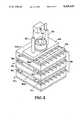
- FIG. 2is a perspective view of a diode array comprising a plurality of thin planar packages connected together.
- FIG. 3is an exploded view of the thin planar package, illustrating its construction in three wafers: a top wafer on which the laser diode bar is mounted, a middle wafer, and a bottom wafer.
- FIG. 4is a sectional view of a portion of the top wafer of the planar package viewed from the bottom, illustrating the microchannel coolers and the coolant manifold.
- FIG. 5is a cross section of the thin package, illustrating the flow of coolant through the package.
- the present inventioncomprises a compact, thin planar package shown generally at 10 in FIG. 2, including a laser diode bar 12 and cooling means internal to the package 10.
- Electric currentis provided to the laser diode bar 12 by a conventional electric current source 14.
- the laser diode bar 12is positioned proximate to the edge 16 so that emitted laser light 18 is substantially unobstructed by the top surface 20.
- Coolantsuch as water is circulated through the package 10 by a conventional coolant circulation system 22. Coolant enters the package 10 through an inlet corridor 24, and exits through an outlet corridor 26.
- FIG. 2illustrates three packages 10a, 10b, 10c; in other embodiments, an array may comprise any number of the packages 10 from two and up.
- the bolt 30is secured by a nut (not shown). Coolant is provided from the coolant circulation system 22 through an inlet tube 35 and an outlet tube 36.
- the thin packages 10are connectable in such close proximity that the laser diode bars 12 are very closely spaced and therefore provide a high intensity laser output 34 over an area as large as the number of packages 10.
- each package 10is constructed of three separate wafers 40,42,44.
- the wafers 40,42,44provide the package 10 that has cooling means integral therein.
- the top wafer 40preferably comprises a silicon substrate
- the middle wafer 42comprises a glass material
- the bottom wafer 44preferably comprises a silicon substrate.
- the bottom wafer 44comprises a manifold 46 that is etched on its top surface.
- the manifold 46may comprise a series of ribs, such as the rib 48 which provides structural strength to the manifold 46.
- the manifold 46forms a passageway for coolant flow between the inlet corridor 24 and a slot 50 formed in the middle wafer 42.
- FIG. 4is a sectional view of a portion of the top wafer 40, viewed from the bottom.
- a manifold 51is formed therein to create a passageway for coolant flow between the outlet corridor 26 and a microchannel heat sink 52.
- a plurality of ribs 53are provided in the manifold 51, which provide structural strength to the manifold 51.
- the heat sink 52is formed in the top wafer 40 proximate to the laser diode bar 12. In that position, the heat sink 52 conducts heat away from the laser diode bar 12, to the coolant flowing through it.
- the heat sink 52comprises a plurality of microchannels 54 formed in the substrate of the silicon wafer 40 in accordance with conventional techniques.
- coolant provided in the inlet corridor 24flows into and through the inlet manifold 46, and then into the slot 50. From there, coolant flows into the microchannel heat sink 52 where heat from the laser diode bar 12 is absorbed. Then, the heated coolant flows through the manifold 51 formed in the top wafer 40, and into the outlet corridor 26 where it is cooled and recirculated by the coolant circulation system 22.
- the inlet corridor 24 and the outlet corridor 26is common to all the planar packages 10 in the array, and thus only a single coolant circulation system 22 (FIG. 2) is required for the entire array.
- the thinness of the wafers 40,42,44is an advantage because the laser diode bars 12 can be positioned in close proximity for high intensity output 34 over a large area, while maintaining a low temperature due to the cooling action of the microchannel heat sinks 52.
- the packages 10appear to be rectangular boxes, in the preferred embodiment the packages 10 are thin planar packages, and therefore can be placed closely together.
- the present inventioncomprises the compact, thin planar package shown generally at 10, including the laser diode bar 12.
- the laser diode bar 12may comprise any of a number of commercially available semiconductor laser diode bars, available from a number of manufacturers such as Siemens AG of Kunststoff, West Germany, and Applied Solar Energy Corp. of City of Industry, Calif.
- the blockWhen a raw diode block is obtained from the manufacturer, the block typically comprises a thin, square piece of semiconductor material, such as Gallium Arsenide (GaAs) with the pn junction formed throughout the square in a plane parallel to the square's surface. Furthermore, the crystal axes in the semiconductor are formed so that they are perpendicular to an edge.
- the individual diode barsare formed by first using a conventional scribe tool, which nicks the edge of the square semiconductor material at fixed intervals. Using the nicks as a guide, the square is separated by a conventional cleaving device into a number of bars by breaking the square along the crystalline axes.
- GaAsGallium Arsenide
- the barsare finally cleaned by conventional plasma ashing, which turns any trace of organic materials into an ash which can be easily removed.
- a smooth facetis formed by this process, which is then made reflective by conventional techniques.
- the output facetis coated with one-half wave thickness Al 2 O 3
- the rear facetis coated with a quarter wave stack of eight layers of TiO 2 /SiO 2 .
- the laser diode bar 12is positioned proximate to the edge 16 so that the emitted laser light 18 is substantially unobstructed by the top surface 20.
- the laser diode bar 12is bonded to the top wafer 40 using a conventional indium solder.
- the laser diode bar 12is clamped to the top wafer 40 by a clamp that has an elastomer edge that presses the length of the bar 12 into tight contact with the evaporated indium solder that was formed on the wafer 40.
- the bar 12 and the wafer 40are then heated enough that the solder melts, and then cooled to form a solid mechanical and electrical bond.
- the diode bar 12is illustrated in the Figures as a single long bar of semiconductor material, in practical application two or more separate shorter bars of semiconductor material, placed end to end, may be utilized instead of the single longer bar.
- Electric currentis provided to the laser diode bar 12 by the conventional electric current source 14.
- the electric currentis delivered through a first terminal 60 provided on the top of the top wafer 40, and a second terminal 62 provided on the bottom of the bottom wafer 44.
- the first terminal 60will be assumed to be the positive terminal 60
- the second terminalwill be assumed to be the negative terminal 62.
- the electric currentflows into the positive terminal 60 and along the top surface of the top wafer 40, via a metallized portion 64.
- the metallized portion 64extends from the terminal 60 to a series of wires 68 which are connected to the laser diode 12.
- the metallized portion 64, and all other metallized portionspreferably comprise a gold conductive layer.
- a thin (1000 ⁇ ) layer of titaniumis formed directly on the wafer 40, and a thin (1000 ⁇ ) layer of platinum is formed on top of the titanium.
- the gold conductive layeris then formed on top of the platinum, in a thickness sufficient to carry the current, for example 1.5 microns.
- the laser diode bar 12connects with the wafer 40
- another 1000 ⁇ layer of titanium or platinumis formed on top of the gold conductive layer
- a thin layer (1000 ⁇ ) of goldis formed on top of the titanium or platinum
- the indium solderis evaporated on top of the thin gold layer, to provide a connection between the top wafer 40 and the laser diode bar 12.
- the top surface of the top wafer 40has a nonconductive electrical break 66, which prevents flow of electrical current. Over this electrical break 66, a series of wires 68, preferably gold wires, electrically connect the metallized portion 64 with an electrode 69 disposed on top of the laser diode bar 12.
- the top electrode 69is the anode
- the bottom electrode 70is the cathode of the laser diode bar 12.
- the electrode 70 on the bottom of the laser diode bar 12is electrically connected to the top wafer 40, in another metallized portion 72. Thus, current flows from the bottom electrode 70, into the metallized surface 72.
- the portion 72 that is metallizedcontinues around the corner of the top wafer 40, and contacts a metallized portion 73 of the middle layer 42, which in turn contacts a metallized portion 74 of the bottom layer 44, which is connected to the negative terminal 62 (FIG. 1).
- a current pathis provided from the laser diode bar 12 along the front edge 16 of the package 10, including a metallized portion 72 of the top wafer 40, the metallized front edge 73 of the middle wafer 42, and the metallized portion 74 of the bottom wafer 44 which is connected to the negative terminal 62 in the preferred embodiment.
- metal clips 76are disposed between adjacent packages 10.
- the metal clip 76adisposed between the package 10a and the adjacent package 10b, electrically connects the metallized bottom surface 74 of the planar package 10a with metallized top portion 64 of the planar package 10 below it.
- the laser diode bars 12are electrically connected in series.
- the electrical current source 14is operated to provide a level of electrical current that provides the desired output intensity.
- a suitable coolant such as wateris circulated through the package 10 by the conventional coolant circulation system 22.
- the planar packages 10 of the preferred embodimenthave been operated with a coolant circulation system 22 that comprises a Neslab chiller that provides 55 psi. However, the planar packages 10 have been tested to withstand a higher pressure, and therefore the coolant circulation system 22 may provide a higher pressure than 55 psi.
- the inlet tube 34 and the outlet tube 36are connected to a header 80, which provides a solid structural connection between the tubes 34,36 and the corridors 24,26.
- a thin gasket 82is disposed between the header 80 and the topmost package 10a.
- the gasket 82comprises a teflon material which provides a watertight seal, such as Gore-tex®.
- coolantcan flow into and out of the corridor 24,26 to provide coolant to the microchannel heat sinks 52 in each of the packages 10.
- the inlet corridor 24comprises holes in the wafers 40,42,44, that are aligned with each other
- the outlet corridor 26comprises holes in the wafers 40,42,44, that are aligned with each other.
- the plurality of packages 10are secured together in a stacked configuration. In this array, the holes in each of the packages 10 are aligned to form a single inlet corridor 24 and a single outlet corridor 26.
- a gasket 84ais positioned to provide a watertight seal.
- a gasket 84bis positioned to provide a watertight seal.
- the gaskets 84a,84bcomprises a teflon material such as Gore-tex®. It is desirable that the gaskets 84a,84b, are thin, because then the packages 10a,10b,10c are positioned in close proximity to each other, and the thickness of the wafers 40,42,44 determine the minimum spacing between the diode bars 12. As a result, the laser diode bars 12 are very closely spaced and therefore the array can provide a high intensity laser output 34. The active cooling of the diode bars 12 permits operation of the laser diode bars 12 at a high average power, in either a pulsed mode or a continuous mode of operation.
- Gore-tex®teflon material
- the coolant circulation system 22may be connected to the bottom by a header similar to the header 80, on the top of the array. Alternately, if the coolant circulation system 22 were to be connected only to the top, then the bottommost package 10 in the array must be plugged by any suitable means in order to retain coolant within the corridors 24,26.
- each package 10is constructed of the three wafers 40,42,44.
- FIG. 4is a perspective view of the top wafer 40, viewed from the bottom.
- the top wafer 40preferably comprises a silicon substrate
- the middle wafer 42comprises a glass material
- the bottom wafer 44preferably comprises a silicon substrate.
- the glass material of the middle wafer 42preferably comprises a glass that is closely matched to the thermal expansion of silicon, for example Corning #7740, or equivalent.
- the wafers 40,42,44are bonded together preferably by an anodic bonding process.
- a first wafer(either the top wafer 40 or the bottom wafer 44) is positioned on a hot plate which also acts as an electrode.
- the middle wafer 42is positioned with respect to the other wafer to produce the desired pattern alignment. Both wafers are heated by the hot plate to a high temperature (for example 550° F.). Then another electrode is electrically connected to the wafer 42, and a high voltage (for example 1200 volts) is applied across the two wafers, which bonds them together.
- the third waferis positioned on top of the middle wafer 42 in the desired pattern alignment, and then heated to a high temperature.
- the first wafercomprises one or more holes (not shown) formed therein in any suitable location. The holes are of sufficient size and location to allow passage of an electrode so that a high voltage can be placed across the middle layer 42 and the third wafer in the bonding process. When the high voltage is applied, bonding occurs between the middle wafer 42 and the third wafer. After bonding is complete, the bonding electrode may be removed.
- the bottom wafer 44comprises the manifold 46 that is etched on its top surface, by conventional anisotropic etching techniques which etch the material along crystal axes. A similar process is used to form the manifold 51, formed in the top wafer 40.
- Each manifold 46,51may comprise a series of ribs, such as the rib 48 which provides structural strength to the manifold 46, and the ribs 53 which provides structural strength to the manifold 51.
- the ribs 48,53are etched along the crystalline axis, preferably at a distance of several tenths of a millimeter (for example 0.25 mm) apart. As illustrated, preferably the ribs 53 are etched in a pattern that promotes coolant flow to the microchannel heat sink 52, the pattern being designed to promote a coolant flow that is approximately even through each of the microchannels 54.
- the heat sink 52is formed in the top wafer 40 proximate to the laser diode bar 12. In that position, the heat sink 52 conducts heat away from the laser diode bar 12, to the coolant flowing through it.
- the microchannel heat sink 52comprises a plurality of microchannels 54 formed in the substrate of the silicon wafer 40 in accordance with conventional techniques. Preferably, the microchannel heat sink 52 is formed by conventional anisotropic etching techniques.
- the microchannelspreferably have dimensions comprising 25 microns in width, 125 microns in depth, and the ribs separating the microchannels are 25 microns in width.
- the middle wafer 42comprises the slot 50 which provides a passageway for coolant flow between the top manifold 51 and the lower manifold 46.
- the slot 50is formed in the middle wafer 42 by ultrasonic milling, using conventional techniques.
- the manifold 46forms a passageway for coolant flow between the inlet corridor 24 and the slot 50 formed in the middle wafer 42.
- the manifold 51 formed in the top wafer 40creates a passageway for coolant flow between the outlet corridor 24 and the microchannel heat sink 52.
- a coolant pathis provided from the inlet corridor 24, through the manifold 46, into the slot 50, then through the microchannel heat sink 52 where heat from the laser diode bar 12 can be absorbed, then through the manifold 51, and to the outlet corridor 26.
- the corridors 24,26have been respectively referred to as "inlet”, and "outlet” corridors, coolant could be made to flow through the package 10 in either direction.
- the present inventionprovides adequate cooling regardless of the direction of coolant flow.
- the packages 10appear to be rectangular boxes, in the preferred embodiment, the packages 10 are much thinner planar packages, and therefore can be placed closely together.
- the present inventionprovides a high intensity output that can be maintained continuously, or at a high average power.
- the top wafer 40, and the bottom wafer 44have been fabricated to have a thickness of 0.017 inch (0.43 mm) each, and the middle wafer has been fabricated to have a thickness of 0.032 inch (0.81 mm).
- the three wafers 40,42,44have a combined thickness of 0.066 inch (1.67 mm).
- a laser diode 12may have a thickness of 0.004 inch (0.1 mm), and the gasket 84 may have a thickness of 0.010 inch (0.25 mm).
- the totalis 0.080 inch (2.02 mm). This figure is a measure of the separation between adjacent laser diodes 12 in the array 34.
- the present inventionprovides sufficient cooling to operate the laser diode in the pulsed mode or continuously at a very high average power output.
- the present inventionhas application as a pump for a high power solid state lasers. Incorporating the present invention in a conventional manner, high power lasers may be produced that the are efficient and inexpensive, and have a small size compared with lasers that are available now.
Landscapes
- Physics & Mathematics (AREA)
- Condensed Matter Physics & Semiconductors (AREA)
- General Physics & Mathematics (AREA)
- Electromagnetism (AREA)
- Optics & Photonics (AREA)
- Cooling Or The Like Of Semiconductors Or Solid State Devices (AREA)
- Semiconductor Lasers (AREA)
Abstract
Description
Claims (14)
Priority Applications (1)
| Application Number | Priority Date | Filing Date | Title |
|---|---|---|---|
| US07/549,509US5105429A (en) | 1990-07-06 | 1990-07-06 | Modular package for cooling a laser diode array |
Applications Claiming Priority (1)
| Application Number | Priority Date | Filing Date | Title |
|---|---|---|---|
| US07/549,509US5105429A (en) | 1990-07-06 | 1990-07-06 | Modular package for cooling a laser diode array |
Publications (1)
| Publication Number | Publication Date |
|---|---|
| US5105429Atrue US5105429A (en) | 1992-04-14 |
Family
ID=24193304
Family Applications (1)
| Application Number | Title | Priority Date | Filing Date |
|---|---|---|---|
| US07/549,509Expired - LifetimeUS5105429A (en) | 1990-07-06 | 1990-07-06 | Modular package for cooling a laser diode array |
Country Status (1)
| Country | Link |
|---|---|
| US (1) | US5105429A (en) |
Cited By (121)
| Publication number | Priority date | Publication date | Assignee | Title |
|---|---|---|---|---|
| US5195102A (en)* | 1991-09-13 | 1993-03-16 | Litton Systems Inc. | Temperature controlled laser diode package |
| US5253260A (en)* | 1991-12-20 | 1993-10-12 | Hughes Aircraft Company | Apparatus and method for passive heat pipe cooling of solid state laser heads |
| US5309457A (en)* | 1992-12-22 | 1994-05-03 | Minch Richard B | Micro-heatpipe cooled laser diode array |
| US5311530A (en)* | 1990-09-14 | 1994-05-10 | Advanced Optoelectronics, Inc. | Semiconductor laser array |
| US5327444A (en)* | 1989-04-20 | 1994-07-05 | Massachusetts Institute Of Technology | Solid state waveguide lasers |
| US5360993A (en)* | 1991-10-21 | 1994-11-01 | Nec Corporation | Cooling unit capable of speedily cooling an integrated circuit chip |
| DE4315580A1 (en)* | 1993-05-11 | 1994-11-17 | Fraunhofer Ges Forschung | Arrangement comprising laser diodes and a cooling system, and method for its production |
| DE4315581A1 (en)* | 1993-05-11 | 1994-11-17 | Fraunhofer Ges Forschung | Laser diodes with cooling system |
| DE4335512A1 (en)* | 1993-10-19 | 1995-06-01 | Daimler Benz Aerospace Ag | Mfr. of silicon microchannel coolers for high-power laser diodes |
| US5453641A (en)* | 1992-12-16 | 1995-09-26 | Sdl, Inc. | Waste heat removal system |
| US5490160A (en)* | 1993-11-22 | 1996-02-06 | Xerox Corporation | Method and apparatus for back facet monitoring of multiple semiconductor laser diodes |
| US5495490A (en)* | 1995-02-28 | 1996-02-27 | Mcdonnell Douglas Corporation | Immersion method and apparatus for cooling a semiconductor laser device |
| US5515391A (en)* | 1994-03-07 | 1996-05-07 | Sdl, Inc. | Thermally balanced diode laser package |
| US5520244A (en)* | 1992-12-16 | 1996-05-28 | Sdl, Inc. | Micropost waste heat removal system |
| US5521931A (en)* | 1993-11-22 | 1996-05-28 | Xerox Corporation | Nonmonolithic arrays of accurately positioned diode lasers |
| US5548605A (en)* | 1995-05-15 | 1996-08-20 | The Regents Of The University Of California | Monolithic microchannel heatsink |
| DE19506093A1 (en)* | 1995-02-22 | 1996-08-29 | Dilas Diodenlaser Gmbh | Diode laser device |
| US5610930A (en)* | 1995-03-02 | 1997-03-11 | Hughes Aircraft Company | Voltage adding diode laser array |
| DE19605302A1 (en)* | 1996-02-14 | 1997-08-21 | Fraunhofer Ges Forschung | Heatsink with a mounting surface for an electronic component |
| US5727618A (en)* | 1993-08-23 | 1998-03-17 | Sdl Inc | Modular microchannel heat exchanger |
| US5734672A (en)* | 1996-08-06 | 1998-03-31 | Cutting Edge Optronics, Inc. | Smart laser diode array assembly and operating method using same |
| US5748654A (en)* | 1996-06-17 | 1998-05-05 | Trw Inc. | Diode array providing either a pulsed or a CW mode of operation of a diode pumped solid state laser |
| US5869778A (en)* | 1993-12-14 | 1999-02-09 | Lsi Logic Corporation | Powder metal heat sink for integrated circuit devices |
| US5869891A (en)* | 1995-12-27 | 1999-02-09 | Lsi Logic Corporation | Powdered metal heat sink with increased surface area |
| GB2329758A (en)* | 1997-09-26 | 1999-03-31 | Marconi Gec Ltd | A semiconductor laser diode bar assembly |
| US5898211A (en)* | 1996-04-30 | 1999-04-27 | Cutting Edge Optronics, Inc. | Laser diode package with heat sink |
| US5909458A (en)* | 1996-11-27 | 1999-06-01 | The Regents Of The University Of California | Low-cost laser diode array |
| US5913108A (en)* | 1998-04-30 | 1999-06-15 | Cutting Edge Optronics, Inc. | Laser diode packaging |
| US5920583A (en)* | 1994-02-22 | 1999-07-06 | Lucent Technologies Inc. | Dual laser with thermoelectric cooling |
| US5923481A (en)* | 1996-11-27 | 1999-07-13 | The Regents Of The University Of California | Microlens frames for laser diode arrays |
| US5986234A (en)* | 1997-03-28 | 1999-11-16 | The Regents Of The University Of California | High removal rate laser-based coating removal system |
| US6043456A (en)* | 1996-05-02 | 2000-03-28 | Heidelberger Druchmaschinen Aktiengesellschaft | Method and device for regulating the temperature in a laser-operated printing plate imaging unit of a printing press, particularly of an offset printing press |
| US6072814A (en)* | 1997-05-30 | 2000-06-06 | Videojet Systems International, Inc | Laser diode module with integral cooling |
| US6091746A (en)* | 1995-11-13 | 2000-07-18 | Commissariat A L'energie Atomique | Assembly of cooled laser diode arrays |
| US6097744A (en)* | 1996-11-22 | 2000-08-01 | Fujitsu Limited | Cooling device of a planar light source |
| US6131650A (en)* | 1999-07-20 | 2000-10-17 | Thermal Corp. | Fluid cooled single phase heat sink |
| US6151341A (en)* | 1997-05-30 | 2000-11-21 | Excel/Quantronix, Inc. | Stackable integrated diode packaging |
| WO2001017080A1 (en)* | 1999-08-31 | 2001-03-08 | Trw, Inc. | Diode array package with homogeneous output |
| US6240116B1 (en) | 1997-08-14 | 2001-05-29 | Sdl, Inc. | Laser diode array assemblies with optimized brightness conservation |
| EP1113543A1 (en)* | 1998-09-24 | 2001-07-04 | Branson Ultrasonics Corporation | Laser diode array |
| US6307871B1 (en) | 1998-09-11 | 2001-10-23 | Cutting Edge Optronics, Inc. | Laser system using phase change material for thermal control |
| DE10018421A1 (en)* | 2000-04-13 | 2001-10-25 | Haas Laser Gmbh & Co Kg | Monitoring system for diode laser unit, measures current and temperature of cooling medium leaving heat sink, to determine value representative of function |
| US6351478B1 (en) | 1998-09-11 | 2002-02-26 | Cutting Edge Optronics, Inc. | Passively cooled solid-state laser |
| US6480514B1 (en)* | 1999-10-21 | 2002-11-12 | Jenoptik Aktiengesellschaft | Device for cooling diode lasers |
| US20030031227A1 (en)* | 2001-07-24 | 2003-02-13 | Hiroshi Takigawa | Light source device for pumping solid-state laser medium |
| US6537351B2 (en)* | 2001-05-29 | 2003-03-25 | Utc Fuel Cells, L.L.C. | Compact light weight condenser assembly |
| US6611540B1 (en) | 1999-07-29 | 2003-08-26 | Otward Maria Mueller | Diode-laser system for hyperpolarized He-3 and Xe-129 gas generation and other applications |
| US6636538B1 (en) | 1999-03-29 | 2003-10-21 | Cutting Edge Optronics, Inc. | Laser diode packaging |
| US6643302B1 (en)* | 1999-07-30 | 2003-11-04 | Fanuc Ltd. | Cooling device and surface emitting device comprising same |
| US6647035B1 (en) | 2000-10-17 | 2003-11-11 | The Regents Of The University Of California | Ruggedized microchannel-cooled laser diode array with self-aligned microlens |
| US6700913B2 (en) | 2001-05-29 | 2004-03-02 | Northrop Grumman Corporation | Low cost high integrity diode laser array |
| US6710926B2 (en) | 2002-04-10 | 2004-03-23 | The Regents Of The University Of California | Cylindrical microlens with an internally reflecting surface and a method of fabrication |
| US6724792B2 (en)* | 2002-09-12 | 2004-04-20 | The Boeing Company | Laser diode arrays with replaceable laser diode bars and methods of removing and replacing laser diode bars |
| US6763050B2 (en) | 2000-03-16 | 2004-07-13 | The Regents Of The University Of California | Method for optical pumping of thin laser media at high average power |
| US6804275B2 (en) | 1998-08-18 | 2004-10-12 | Hamamatsu Photonics K.K. | Heat sink and semiconductor laser apparatus and semiconductor laser stack apparatus using the same |
| US20040258123A1 (en)* | 2003-06-23 | 2004-12-23 | Zamel James Michael | Diode-pumped solid-state laser gain module |
| US20050018742A1 (en)* | 2003-07-24 | 2005-01-27 | Hall Daniel F. | Cast laser optical bench |
| US20050018748A1 (en)* | 2003-07-24 | 2005-01-27 | Ringermacher Harry Israel | Actively quenched lamp, infrared thermography imaging system, and method for actively controlling flash duration |
| US6895026B2 (en)* | 1998-08-18 | 2005-05-17 | Hamamatsu Photonics K.K. | Heat sink and semiconductor laser apparatus and semiconductor laser stack apparatus using the same |
| US6898222B2 (en) | 2000-12-06 | 2005-05-24 | Jenoptik Laserdiode Gmbh | Diode laser arrangement with a plurality of diode laser arrays |
| US20050141575A1 (en)* | 2003-12-22 | 2005-06-30 | Dirk Lorenzen | Diode laser subelement and arrangements with such diode laser subelement |
| US20050142394A1 (en)* | 2003-12-30 | 2005-06-30 | Irene Spitsberg | Thermal barrier coatings with lower porosity for improved impact and erosion resistance |
| US20050151140A1 (en)* | 2002-03-06 | 2005-07-14 | Takayoshi Honma | Semiconductor light emitting device and plant cultivating system |
| JP2005535142A (en)* | 2002-07-30 | 2005-11-17 | オスラム オプト セミコンダクターズ ゲゼルシャフト ミット ベシュレンクテル ハフツング | Semiconductor device with cooling element |
| US6970485B1 (en) | 2000-10-20 | 2005-11-29 | Mitsubishi Denki Kabushiki Kaisha | Cooling device, semiconductor laser light source device, semiconductor laser source unit, method of manufacturing semiconductor laser light source unit and solid state laser device |
| WO2005093858A3 (en)* | 2004-03-29 | 2006-06-15 | Platsch Gmbh & Co Kg | Flat uv light source |
| US20060203866A1 (en)* | 2005-03-10 | 2006-09-14 | Northrop Grumman | Laser diode package with an internal fluid cooling channel |
| US20060215715A1 (en)* | 2003-02-27 | 2006-09-28 | Hikaru Kouta | Heat sink, laser module, laser device, and laser-processing device |
| US20060227827A1 (en)* | 2005-04-12 | 2006-10-12 | Hidekazu Kawanishi | Semiconductor laser device and heat sink used therein |
| US20060285076A1 (en)* | 2005-06-20 | 2006-12-21 | Seiko Epson Corporation | Laser source device, display device, and projector |
| US20080025357A1 (en)* | 2006-07-26 | 2008-01-31 | Northrop Grumman Corporation | Microchannel cooler for high efficiency laser diode heat extraction |
| CN100370659C (en)* | 2005-04-18 | 2008-02-20 | 中国科学院长春光学精密机械与物理研究所 | Microchannel heat sink structure and preparation method for semiconductor laser head pump source |
| US20080056314A1 (en)* | 2006-08-31 | 2008-03-06 | Northrop Grumman Corporation | High-power laser-diode package system |
| US20080089371A1 (en)* | 2006-10-11 | 2008-04-17 | Patrick Reichert | Bright light source with two-dimensional array of diode-laser emitters |
| US20080123705A1 (en)* | 2006-11-02 | 2008-05-29 | David Schleuning | Thermally tuned diode-laser bar package |
| DE102007028403A1 (en)* | 2007-06-17 | 2008-12-24 | Platsch Gmbh & Co.Kg | Ultraviolet dryer, particularly for drying of color coats of printing products, has carrying body, at which multiple ultraviolet light emitting diodes are attached |
| DE102007051798B3 (en)* | 2007-10-26 | 2009-01-15 | Jenoptik Laserdiode Gmbh | Micro-channel heat sink for cooling semiconductor laser component, has electrically isolating inorganic protective layer or closing protective layer formed from metal and applied on sealing surfaces and inner surfaces of inlet and outlet |
| US20090161709A1 (en)* | 2007-12-20 | 2009-06-25 | International Business Machines Corporation | Multichip package, methods of manufacture thereof and articles comprising the same |
| US20090185592A1 (en)* | 2008-01-18 | 2009-07-23 | Jan Vetrovec | Laser diode system with reduced coolant consumption |
| US20090185593A1 (en)* | 2008-01-18 | 2009-07-23 | Northrop Grumman Space & Mission Systems Corp. | Method of manufacturing laser diode packages and arrays |
| EP2110903A2 (en) | 2008-04-17 | 2009-10-21 | Lasertel Inc. | Liquid cooled laser bar arrays incorporating diamond/copper expansion matched materials |
| DE102008051081A1 (en)* | 2008-10-09 | 2010-05-12 | Dirk Dr. Lorenzen | Heat dissipation module, has semiconductor emitter arranged between heat dissipating bodies, where one of bodies is provided to side of semiconductor emitter and no channel extends for conducting cooling fluid within area of side |
| US20100156311A1 (en)* | 2007-02-04 | 2010-06-24 | Tottori University | Electronic Device and Light Emission Control Method For Electronic Device |
| US20100175853A1 (en)* | 2007-11-16 | 2010-07-15 | Iq Evolution Gmbh | Multi-component cooling element |
| US20100183039A1 (en)* | 2009-01-21 | 2010-07-22 | Coherent, Inc. | Two-dimensional diode-laser array with broad-band output |
| DE10047780B4 (en)* | 1999-10-21 | 2010-08-05 | Jenoptik Ag | Device for cooling diode lasers |
| US20100208431A1 (en)* | 2008-10-09 | 2010-08-19 | Dugas Matthew P | Patterned Composite Structures and Methods of Making the Same |
| WO2010015352A3 (en)* | 2008-08-05 | 2010-08-26 | Jenoptik Laserdiode Gmbh | Heat dissipation module having a semiconductor element and production method for such a heat dissipation module |
| US20100300550A1 (en)* | 2002-08-15 | 2010-12-02 | Velocys, Inc. | Multi-Stream Microchannel Device |
| US20110019210A1 (en)* | 2008-05-06 | 2011-01-27 | Chung Bradley D | Printhead feed slot ribs |
| US20110026551A1 (en)* | 2009-07-28 | 2011-02-03 | Northrop Grumman Systems Corp. | Laser Diode Ceramic Cooler Having Circuitry For Control And Feedback Of Laser Diode Performance |
| WO2011022923A1 (en)* | 2009-08-31 | 2011-03-03 | 西安炬光科技有限公司 | Cooling module for laser, manufacture method thereof and semiconductor laser including the same |
| US20110204261A1 (en)* | 2010-01-27 | 2011-08-25 | FUSION UV SYSTEMS, INC. A Delaware Corporation | Micro-channel-cooled high heat load light emitting device |
| US20120267074A1 (en)* | 2011-04-19 | 2012-10-25 | Kabushiki Kaisha Toyota Jidoshokki | Cooling device |
| WO2012166678A1 (en)* | 2011-05-27 | 2012-12-06 | Lockheed Martin Corporation | Fluid-cooled module for integrated circuit devices |
| US8721135B2 (en) | 2010-12-21 | 2014-05-13 | Anthony DeRose | Fluid cooled lighting element |
| US20140204968A1 (en)* | 2009-08-31 | 2014-07-24 | Xi'an Focuslight Technologies Co., Ltd. | Cooling module for laser, fabricating method thereof, and semiconductor laser fabricated from the module |
| US8804782B2 (en) | 2012-10-29 | 2014-08-12 | Coherent, Inc. | Macro-channel water-cooled heat-sink for diode-laser bars |
| US8804781B2 (en)* | 2012-10-29 | 2014-08-12 | Coherent, Inc. | Macro channel water-cooled heat-sink for diode-laser bars |
| US8937976B2 (en) | 2012-08-15 | 2015-01-20 | Northrop Grumman Systems Corp. | Tunable system for generating an optical pulse based on a double-pass semiconductor optical amplifier |
| DE102015002176A1 (en) | 2015-02-24 | 2016-08-25 | Jenoptik Laser Gmbh | Method of making a diode laser and diode laser |
| EP3101744A1 (en) | 2015-06-02 | 2016-12-07 | Lasertel Inc. | Liquid cooled laser bar arrays incorporating thermal expansion matched materials |
| US9590388B2 (en) | 2011-01-11 | 2017-03-07 | Northrop Grumman Systems Corp. | Microchannel cooler for a single laser diode emitter based system |
| CN107148705A (en)* | 2014-10-22 | 2017-09-08 | 三菱电机株式会社 | Laser light source device |
| WO2018060134A1 (en)* | 2016-09-27 | 2018-04-05 | Jenoptik Laser Gmbh | Optical and optoelectronic assembly and method for the production thereof |
| US9941658B2 (en) | 2016-05-24 | 2018-04-10 | Coherent, Inc. | Stackable electrically-isolated diode-laser bar assembly |
| US10094549B2 (en) | 2012-08-22 | 2018-10-09 | Flex-N-Gate Advanced Product Development, Llc | Micro-channel heat sink for LED headlamp |
| CN108666869A (en)* | 2017-03-29 | 2018-10-16 | 山东华光光电子股份有限公司 | A kind of feux rouges high power laser module and its assemble method |
| WO2019086619A1 (en) | 2017-11-03 | 2019-05-09 | Jenoptik Laser Gmbh | Diode laser |
| CN110364917A (en)* | 2018-04-11 | 2019-10-22 | 深圳联品激光技术有限公司 | A laser and cooling device |
| US10777966B1 (en) | 2017-12-18 | 2020-09-15 | Lockheed Martin Corporation | Mixed-flow cooling to maintain cooling requirements |
| WO2021052937A1 (en) | 2019-09-16 | 2021-03-25 | Jenoptik Optical Systems Gmbh | Method for producing a semiconductor assembly and diode laser |
| US11056854B2 (en) | 2018-08-14 | 2021-07-06 | Leonardo Electronics Us Inc. | Laser assembly and related methods |
| EP3809542A4 (en)* | 2018-06-14 | 2021-07-28 | Fujikura Ltd. | OPTICAL MODULAR UNIT AND LASER DEVICE |
| US11095084B1 (en)* | 2019-02-07 | 2021-08-17 | Panasonic Intellectual Property Management Co., Ltd. | Laser system with isolated optical cavity |
| US11296481B2 (en) | 2019-01-09 | 2022-04-05 | Leonardo Electronics Us Inc. | Divergence reshaping array |
| US11406004B2 (en) | 2018-08-13 | 2022-08-02 | Leonardo Electronics Us Inc. | Use of metal-core printed circuit board (PCB) for generation of ultra-narrow, high-current pulse driver |
| WO2023110389A1 (en) | 2021-12-17 | 2023-06-22 | Jenoptik Optical Systems Gmbh | Method for producing a diode laser, and diode laser |
| US11705690B2 (en) | 2016-11-29 | 2023-07-18 | Leonardo Electronics Us Inc. | Dual junction fiber-coupled laser diode and related methods |
| US11752571B1 (en) | 2019-06-07 | 2023-09-12 | Leonardo Electronics Us Inc. | Coherent beam coupler |
| US12253685B2 (en) | 2019-09-16 | 2025-03-18 | Leonardo Electronics Us Inc. | Asymmetric input intensity hexagonal homogenizer |
Citations (13)
| Publication number | Priority date | Publication date | Assignee | Title |
|---|---|---|---|---|
| US4315225A (en)* | 1979-08-24 | 1982-02-09 | Mcdonnell Douglas Corporation | Heat sink laser diode array |
| US4393393A (en)* | 1979-08-13 | 1983-07-12 | Mcdonnell Douglas Corporation | Laser diode with double sided heat sink |
| US4574470A (en)* | 1984-03-19 | 1986-03-11 | Trilogy Computer Development Partners, Ltd. | Semiconductor chip mounting system |
| US4589116A (en)* | 1983-08-11 | 1986-05-13 | Siemens Aktiengesellschaft | Laser diode with uniform mechanical stress and/or heat dissipation |
| US4592059A (en)* | 1983-08-23 | 1986-05-27 | Siemens Aktiengesellschaft | Laser diode with simplified adjustment during assembly |
| US4627062A (en)* | 1983-10-26 | 1986-12-02 | Mcdonnell Douglas Corporation | AC driven laser diode array, power supply, transformer, and method therefor |
| US4672736A (en)* | 1984-09-26 | 1987-06-16 | Siemens Aktiengesellschaft | Method for producing laser diodes with an adjusted and integrated heat sink |
| US4758926A (en)* | 1986-03-31 | 1988-07-19 | Microelectronics And Computer Technology Corporation | Fluid-cooled integrated circuit package |
| US4791634A (en)* | 1987-09-29 | 1988-12-13 | Spectra-Physics, Inc. | Capillary heat pipe cooled diode pumped slab laser |
| US4809058A (en)* | 1985-12-16 | 1989-02-28 | Hitachi, Ltd. | Integrated circuit device |
| US4881237A (en)* | 1988-08-26 | 1989-11-14 | Massachusetts Institute Of Technology | Hybrid two-dimensional surface-emitting laser arrays |
| US4894709A (en)* | 1988-03-09 | 1990-01-16 | Massachusetts Institute Of Technology | Forced-convection, liquid-cooled, microchannel heat sinks |
| US4956746A (en)* | 1989-03-29 | 1990-09-11 | Hughes Aircraft Company | Stacked wafer electronic package |
- 1990
- 1990-07-06USUS07/549,509patent/US5105429A/ennot_activeExpired - Lifetime
Patent Citations (13)
| Publication number | Priority date | Publication date | Assignee | Title |
|---|---|---|---|---|
| US4393393A (en)* | 1979-08-13 | 1983-07-12 | Mcdonnell Douglas Corporation | Laser diode with double sided heat sink |
| US4315225A (en)* | 1979-08-24 | 1982-02-09 | Mcdonnell Douglas Corporation | Heat sink laser diode array |
| US4589116A (en)* | 1983-08-11 | 1986-05-13 | Siemens Aktiengesellschaft | Laser diode with uniform mechanical stress and/or heat dissipation |
| US4592059A (en)* | 1983-08-23 | 1986-05-27 | Siemens Aktiengesellschaft | Laser diode with simplified adjustment during assembly |
| US4627062A (en)* | 1983-10-26 | 1986-12-02 | Mcdonnell Douglas Corporation | AC driven laser diode array, power supply, transformer, and method therefor |
| US4574470A (en)* | 1984-03-19 | 1986-03-11 | Trilogy Computer Development Partners, Ltd. | Semiconductor chip mounting system |
| US4672736A (en)* | 1984-09-26 | 1987-06-16 | Siemens Aktiengesellschaft | Method for producing laser diodes with an adjusted and integrated heat sink |
| US4809058A (en)* | 1985-12-16 | 1989-02-28 | Hitachi, Ltd. | Integrated circuit device |
| US4758926A (en)* | 1986-03-31 | 1988-07-19 | Microelectronics And Computer Technology Corporation | Fluid-cooled integrated circuit package |
| US4791634A (en)* | 1987-09-29 | 1988-12-13 | Spectra-Physics, Inc. | Capillary heat pipe cooled diode pumped slab laser |
| US4894709A (en)* | 1988-03-09 | 1990-01-16 | Massachusetts Institute Of Technology | Forced-convection, liquid-cooled, microchannel heat sinks |
| US4881237A (en)* | 1988-08-26 | 1989-11-14 | Massachusetts Institute Of Technology | Hybrid two-dimensional surface-emitting laser arrays |
| US4956746A (en)* | 1989-03-29 | 1990-09-11 | Hughes Aircraft Company | Stacked wafer electronic package |
Non-Patent Citations (18)
| Title |
|---|
| D. B. Tuckerman et al., "High Performance Heat Sinking for VLSI", IEE Elec. Device Lett., vol. EDL-2, No. 5, pp. 126-129, May, 1981. |
| D. B. Tuckerman et al., High Performance Heat Sinking for VLSI , IEE Elec. Device Lett., vol. EDL 2, No. 5, pp. 126 129, May, 1981.* |
| D. B. Tuckerman, "Heat -Transfer Microstructures for Integrated Circuits", Ph.D. Thesis, Stanford Uni., UCRL-53515, Feb. 1984). |
| D. B. Tuckerman, Heat Transfer Microstructures for Integrated Circuits , Ph.D. Thesis, Stanford Uni., UCRL 53515, Feb. 1984).* |
| D. Mundinger et al., "High Average Power 20D Laser Diode Arrays on Silicon Microchannel Coolers", Conf. on Lasers and Electro-Optics, Baltimore, Md., Apr. 24-28, 1989. |
| D. Mundinger et al., "Laser Diode Coolign for High Average Power Applications", SPIE OE Lase 89, Los Angeles, Calif. Feb. 15-20, 1989. |
| D. Mundinger et al., High Average Power 20D Laser Diode Arrays on Silicon Microchannel Coolers , Conf. on Lasers and Electro Optics, Baltimore, Md., Apr. 24 28, 1989.* |
| D. Mundinger et al., Laser Diode Coolign for High Average Power Applications , SPIE OE Lase 89, Los Angeles, Calif. Feb. 15 20, 1989.* |
| J. P. Donnelly et al., "Hybrid Approach to Two-Dimensional Surface-Emitting Diode Laser Arrays", Appl. Phys. Lett., vol. 53, No. 11, pp. 938-940, (1988). |
| J. P. Donnelly et al., Hybrid Approach to Two Dimensional Surface Emitting Diode Laser Arrays , Appl. Phys. Lett., vol. 53, No. 11, pp. 938 940, (1988).* |
| M. G. Grote et al., "Test Results of Wafer Thin Coolers at Heat Fluxes from 5 to 125W/cm2", P#880997, Soc. of Automotive Engineering, San Francisco, Calif., Jul. 1986. |
| M. G. Grote et al., Test Results of Wafer Thin Coolers at Heat Fluxes from 5 to 125W/cm 2 , P 880997, Soc. of Automotive Engineering, San Francisco, Calif., Jul. 1986.* |
| R. Beach et al., "High Reliability Silicon Microchannel Submount for High erage Power Laser Diode Arrays", Appl. Phys. Lett., vol. 56, p. 2065, May 21, 1990. |
| R. Beach et al., High Reliability Silicon Microchannel Submount for High Average Power Laser Diode Arrays , Appl. Phys. Lett., vol. 56, p. 2065, May 21, 1990.* |
| R. J. Phillips, "Microchannel Heat Sinks", The Lincoln Lab J., vol. 1, No. 1, pp. 31-48, (1988). |
| R. J. Phillips, Microchannel Heat Sinks , The Lincoln Lab J., vol. 1, No. 1, pp. 31 48, (1988).* |
| T. J. Bland et al., "A Compact High Intensity Cooler", P#831127, 13th Intersociety Conf. on Env. Systems, San Francisco, Calif., Jul. 11-13, 1983. |
| T. J. Bland et al., A Compact High Intensity Cooler , P 831127, 13th Intersociety Conf. on Env. Systems, San Francisco, Calif., Jul. 11 13, 1983.* |
Cited By (192)
| Publication number | Priority date | Publication date | Assignee | Title |
|---|---|---|---|---|
| US5327444A (en)* | 1989-04-20 | 1994-07-05 | Massachusetts Institute Of Technology | Solid state waveguide lasers |
| US5311530A (en)* | 1990-09-14 | 1994-05-10 | Advanced Optoelectronics, Inc. | Semiconductor laser array |
| US5195102A (en)* | 1991-09-13 | 1993-03-16 | Litton Systems Inc. | Temperature controlled laser diode package |
| US5360993A (en)* | 1991-10-21 | 1994-11-01 | Nec Corporation | Cooling unit capable of speedily cooling an integrated circuit chip |
| US5253260A (en)* | 1991-12-20 | 1993-10-12 | Hughes Aircraft Company | Apparatus and method for passive heat pipe cooling of solid state laser heads |
| US5453641A (en)* | 1992-12-16 | 1995-09-26 | Sdl, Inc. | Waste heat removal system |
| US5520244A (en)* | 1992-12-16 | 1996-05-28 | Sdl, Inc. | Micropost waste heat removal system |
| US5309457A (en)* | 1992-12-22 | 1994-05-03 | Minch Richard B | Micro-heatpipe cooled laser diode array |
| DE4315580A1 (en)* | 1993-05-11 | 1994-11-17 | Fraunhofer Ges Forschung | Arrangement comprising laser diodes and a cooling system, and method for its production |
| DE4315581A1 (en)* | 1993-05-11 | 1994-11-17 | Fraunhofer Ges Forschung | Laser diodes with cooling system |
| US5727618A (en)* | 1993-08-23 | 1998-03-17 | Sdl Inc | Modular microchannel heat exchanger |
| DE4335512A1 (en)* | 1993-10-19 | 1995-06-01 | Daimler Benz Aerospace Ag | Mfr. of silicon microchannel coolers for high-power laser diodes |
| US5490160A (en)* | 1993-11-22 | 1996-02-06 | Xerox Corporation | Method and apparatus for back facet monitoring of multiple semiconductor laser diodes |
| US5521931A (en)* | 1993-11-22 | 1996-05-28 | Xerox Corporation | Nonmonolithic arrays of accurately positioned diode lasers |
| US5869778A (en)* | 1993-12-14 | 1999-02-09 | Lsi Logic Corporation | Powder metal heat sink for integrated circuit devices |
| US5920583A (en)* | 1994-02-22 | 1999-07-06 | Lucent Technologies Inc. | Dual laser with thermoelectric cooling |
| US5515391A (en)* | 1994-03-07 | 1996-05-07 | Sdl, Inc. | Thermally balanced diode laser package |
| DE19506093C2 (en)* | 1995-02-22 | 2000-12-07 | Dilas Diodenlaser Gmbh | Diode laser device |
| DE19506093A1 (en)* | 1995-02-22 | 1996-08-29 | Dilas Diodenlaser Gmbh | Diode laser device |
| US5495490A (en)* | 1995-02-28 | 1996-02-27 | Mcdonnell Douglas Corporation | Immersion method and apparatus for cooling a semiconductor laser device |
| US5610930A (en)* | 1995-03-02 | 1997-03-11 | Hughes Aircraft Company | Voltage adding diode laser array |
| US5548605A (en)* | 1995-05-15 | 1996-08-20 | The Regents Of The University Of California | Monolithic microchannel heatsink |
| US6091746A (en)* | 1995-11-13 | 2000-07-18 | Commissariat A L'energie Atomique | Assembly of cooled laser diode arrays |
| US5869891A (en)* | 1995-12-27 | 1999-02-09 | Lsi Logic Corporation | Powdered metal heat sink with increased surface area |
| DE19605302A1 (en)* | 1996-02-14 | 1997-08-21 | Fraunhofer Ges Forschung | Heatsink with a mounting surface for an electronic component |
| US5898211A (en)* | 1996-04-30 | 1999-04-27 | Cutting Edge Optronics, Inc. | Laser diode package with heat sink |
| US5985684A (en)* | 1996-04-30 | 1999-11-16 | Cutting Edge Optronics, Inc. | Process for manufacturing a laser diode having a heat sink |
| US6043456A (en)* | 1996-05-02 | 2000-03-28 | Heidelberger Druchmaschinen Aktiengesellschaft | Method and device for regulating the temperature in a laser-operated printing plate imaging unit of a printing press, particularly of an offset printing press |
| US5748654A (en)* | 1996-06-17 | 1998-05-05 | Trw Inc. | Diode array providing either a pulsed or a CW mode of operation of a diode pumped solid state laser |
| US6144684A (en)* | 1996-08-06 | 2000-11-07 | Cutting Edge Optronics, Inc. | Smart laser diode array assembly |
| US5734672A (en)* | 1996-08-06 | 1998-03-31 | Cutting Edge Optronics, Inc. | Smart laser diode array assembly and operating method using same |
| US6385226B2 (en) | 1996-08-06 | 2002-05-07 | Trw Inc. | Smart laser diode array assembly |
| US6272164B1 (en) | 1996-08-06 | 2001-08-07 | Cutting Edge Optronics, Inc. | Smart laser diode array assembly |
| US6266881B1 (en) | 1996-11-22 | 2001-07-31 | Fujitsu Limited | Method of making a cooling device of a planar light source |
| US6245589B1 (en)* | 1996-11-22 | 2001-06-12 | Fujitsu Limited | Fabrication of cooling device of a planar light source |
| US6387286B1 (en)* | 1996-11-22 | 2002-05-14 | Fanuc, Ltd. | Cooling device of a planar light source |
| US6097744A (en)* | 1996-11-22 | 2000-08-01 | Fujitsu Limited | Cooling device of a planar light source |
| DE19750879B4 (en)* | 1996-11-22 | 2005-07-21 | Fanuc Ltd. | Cooling device for a linear light source, linear light source and planar light source assembled therefrom, and manufacturing method therefor |
| US5909458A (en)* | 1996-11-27 | 1999-06-01 | The Regents Of The University Of California | Low-cost laser diode array |
| US5923481A (en)* | 1996-11-27 | 1999-07-13 | The Regents Of The University Of California | Microlens frames for laser diode arrays |
| US5986234A (en)* | 1997-03-28 | 1999-11-16 | The Regents Of The University Of California | High removal rate laser-based coating removal system |
| US6151341A (en)* | 1997-05-30 | 2000-11-21 | Excel/Quantronix, Inc. | Stackable integrated diode packaging |
| US6072814A (en)* | 1997-05-30 | 2000-06-06 | Videojet Systems International, Inc | Laser diode module with integral cooling |
| US6240116B1 (en) | 1997-08-14 | 2001-05-29 | Sdl, Inc. | Laser diode array assemblies with optimized brightness conservation |
| GB2329758A (en)* | 1997-09-26 | 1999-03-31 | Marconi Gec Ltd | A semiconductor laser diode bar assembly |
| GB2329758B (en)* | 1997-09-26 | 1999-08-25 | Gec Marconi Avionics Holdings | A semiconductor laser diode bar assembly |
| US6310900B1 (en) | 1998-04-30 | 2001-10-30 | Cutting Edge Optronics, Inc. | Laser diode package with heat sink |
| US5913108A (en)* | 1998-04-30 | 1999-06-15 | Cutting Edge Optronics, Inc. | Laser diode packaging |
| US6895026B2 (en)* | 1998-08-18 | 2005-05-17 | Hamamatsu Photonics K.K. | Heat sink and semiconductor laser apparatus and semiconductor laser stack apparatus using the same |
| US6804275B2 (en) | 1998-08-18 | 2004-10-12 | Hamamatsu Photonics K.K. | Heat sink and semiconductor laser apparatus and semiconductor laser stack apparatus using the same |
| US6351478B1 (en) | 1998-09-11 | 2002-02-26 | Cutting Edge Optronics, Inc. | Passively cooled solid-state laser |
| US6307871B1 (en) | 1998-09-11 | 2001-10-23 | Cutting Edge Optronics, Inc. | Laser system using phase change material for thermal control |
| US6570895B2 (en) | 1998-09-11 | 2003-05-27 | Cutting Edge Optronics, Inc. | Laser system using phase change material for thermal control |
| EP1113543A1 (en)* | 1998-09-24 | 2001-07-04 | Branson Ultrasonics Corporation | Laser diode array |
| US6636538B1 (en) | 1999-03-29 | 2003-10-21 | Cutting Edge Optronics, Inc. | Laser diode packaging |
| US20060186500A1 (en)* | 1999-03-29 | 2006-08-24 | Stephens Edward F | Laser diode packaging |
| US7361978B2 (en) | 1999-03-29 | 2008-04-22 | Northrop Gruman Corporation | Laser diode packaging |
| US7060515B2 (en) | 1999-03-29 | 2006-06-13 | Cutting Edge Optronics, Inc. | Method of manufacturing a laser diode package |
| US20040082112A1 (en)* | 1999-03-29 | 2004-04-29 | Stephens Edward F. | Laser diode packaging |
| US6131650A (en)* | 1999-07-20 | 2000-10-17 | Thermal Corp. | Fluid cooled single phase heat sink |
| US6611540B1 (en) | 1999-07-29 | 2003-08-26 | Otward Maria Mueller | Diode-laser system for hyperpolarized He-3 and Xe-129 gas generation and other applications |
| US6643302B1 (en)* | 1999-07-30 | 2003-11-04 | Fanuc Ltd. | Cooling device and surface emitting device comprising same |
| WO2001017080A1 (en)* | 1999-08-31 | 2001-03-08 | Trw, Inc. | Diode array package with homogeneous output |
| DE10047780B4 (en)* | 1999-10-21 | 2010-08-05 | Jenoptik Ag | Device for cooling diode lasers |
| US6480514B1 (en)* | 1999-10-21 | 2002-11-12 | Jenoptik Aktiengesellschaft | Device for cooling diode lasers |
| US6763050B2 (en) | 2000-03-16 | 2004-07-13 | The Regents Of The University Of California | Method for optical pumping of thin laser media at high average power |
| US20030043867A1 (en)* | 2000-04-13 | 2003-03-06 | Trumpf Laser Gmbh + Co. Kg | Diode laser device with cooling and operation monitoring |
| DE10018421A1 (en)* | 2000-04-13 | 2001-10-25 | Haas Laser Gmbh & Co Kg | Monitoring system for diode laser unit, measures current and temperature of cooling medium leaving heat sink, to determine value representative of function |
| US6785310B2 (en)* | 2000-04-13 | 2004-08-31 | Trumpf Laser Gmbh + Co. Kg | Diode laser device with cooling and operation monitoring |
| US6647035B1 (en) | 2000-10-17 | 2003-11-11 | The Regents Of The University Of California | Ruggedized microchannel-cooled laser diode array with self-aligned microlens |
| EP1253685A4 (en)* | 2000-10-20 | 2006-09-20 | Mitsubishi Electric Corp | COOLER, SEMICONDUCTOR LASER SOURCE, SEMICONDUCTOR LASER LIGHT SOURCE UNIT, METHOD OF MANUFACTURING A SEMICONDUCTOR LASER LIGHT SOURCE UNIT AND A SOLID STATE LASER. |
| US6970485B1 (en) | 2000-10-20 | 2005-11-29 | Mitsubishi Denki Kabushiki Kaisha | Cooling device, semiconductor laser light source device, semiconductor laser source unit, method of manufacturing semiconductor laser light source unit and solid state laser device |
| US6898222B2 (en) | 2000-12-06 | 2005-05-24 | Jenoptik Laserdiode Gmbh | Diode laser arrangement with a plurality of diode laser arrays |
| US6537351B2 (en)* | 2001-05-29 | 2003-03-25 | Utc Fuel Cells, L.L.C. | Compact light weight condenser assembly |
| US6700913B2 (en) | 2001-05-29 | 2004-03-02 | Northrop Grumman Corporation | Low cost high integrity diode laser array |
| US6850549B2 (en)* | 2001-07-24 | 2005-02-01 | Fanuc Ltd. | Light source device for pumping solid-state laser medium |
| US20030031227A1 (en)* | 2001-07-24 | 2003-02-13 | Hiroshi Takigawa | Light source device for pumping solid-state laser medium |
| US7466023B2 (en)* | 2002-03-06 | 2008-12-16 | Hamamatsu Photonics K.K. | Semiconductor light emitting device and plant cultivating system |
| US20050151140A1 (en)* | 2002-03-06 | 2005-07-14 | Takayoshi Honma | Semiconductor light emitting device and plant cultivating system |
| US6710926B2 (en) | 2002-04-10 | 2004-03-23 | The Regents Of The University Of California | Cylindrical microlens with an internally reflecting surface and a method of fabrication |
| US6948341B2 (en) | 2002-04-10 | 2005-09-27 | The Regents Of The University Of California | Cylindrical microlens with an internally reflecting surface and a method of fabrication |
| US20040129025A1 (en)* | 2002-04-10 | 2004-07-08 | Beach Raymond J. | Cylindrical microlens with an internally reflecting surface and a method of fabrication |
| JP2005535142A (en)* | 2002-07-30 | 2005-11-17 | オスラム オプト セミコンダクターズ ゲゼルシャフト ミット ベシュレンクテル ハフツング | Semiconductor device with cooling element |
| US20100300550A1 (en)* | 2002-08-15 | 2010-12-02 | Velocys, Inc. | Multi-Stream Microchannel Device |
| US7145927B2 (en) | 2002-09-12 | 2006-12-05 | The Boeing Company | Laser diode arrays with replaceable laser diode bars and methods of removing and replacing laser diode bars |
| US6724792B2 (en)* | 2002-09-12 | 2004-04-20 | The Boeing Company | Laser diode arrays with replaceable laser diode bars and methods of removing and replacing laser diode bars |
| US20040165628A1 (en)* | 2002-09-12 | 2004-08-26 | The Boeing Company | Laser diode arrays with replaceable laser diode bars and methods of removing and replacing laser diode bars |
| US20060215715A1 (en)* | 2003-02-27 | 2006-09-28 | Hikaru Kouta | Heat sink, laser module, laser device, and laser-processing device |
| US7170919B2 (en) | 2003-06-23 | 2007-01-30 | Northrop Grumman Corporation | Diode-pumped solid-state laser gain module |
| US20040258123A1 (en)* | 2003-06-23 | 2004-12-23 | Zamel James Michael | Diode-pumped solid-state laser gain module |
| US20050018742A1 (en)* | 2003-07-24 | 2005-01-27 | Hall Daniel F. | Cast laser optical bench |
| US20050018748A1 (en)* | 2003-07-24 | 2005-01-27 | Ringermacher Harry Israel | Actively quenched lamp, infrared thermography imaging system, and method for actively controlling flash duration |
| US7495848B2 (en) | 2003-07-24 | 2009-02-24 | Northrop Grumman Corporation | Cast laser optical bench |
| US7369589B2 (en)* | 2003-12-22 | 2008-05-06 | Jenoptik Laserdiode Gmbh | Diode laser subelement and arrangements with such diode laser subelement |
| US20050141575A1 (en)* | 2003-12-22 | 2005-06-30 | Dirk Lorenzen | Diode laser subelement and arrangements with such diode laser subelement |
| US20050142394A1 (en)* | 2003-12-30 | 2005-06-30 | Irene Spitsberg | Thermal barrier coatings with lower porosity for improved impact and erosion resistance |
| US7910899B2 (en) | 2004-03-29 | 2011-03-22 | Platsch Gmbh & Co. Kg | Flat UV light source |
| US20080315132A1 (en)* | 2004-03-29 | 2008-12-25 | Platsch Hans G | Flat Uv Light Source |
| WO2005093858A3 (en)* | 2004-03-29 | 2006-06-15 | Platsch Gmbh & Co Kg | Flat uv light source |
| US7305016B2 (en) | 2005-03-10 | 2007-12-04 | Northrop Grumman Corporation | Laser diode package with an internal fluid cooling channel |
| US20060203866A1 (en)* | 2005-03-10 | 2006-09-14 | Northrop Grumman | Laser diode package with an internal fluid cooling channel |
| US7466732B2 (en) | 2005-03-10 | 2008-12-16 | Northrop Grumman Corporation | Laser diode package with an internal fluid cooling channel |
| US8208510B2 (en)* | 2005-04-12 | 2012-06-26 | Sony Corporation | Semiconductor laser device and heat sink used therein |
| US20060227827A1 (en)* | 2005-04-12 | 2006-10-12 | Hidekazu Kawanishi | Semiconductor laser device and heat sink used therein |
| CN100370659C (en)* | 2005-04-18 | 2008-02-20 | 中国科学院长春光学精密机械与物理研究所 | Microchannel heat sink structure and preparation method for semiconductor laser head pump source |
| US7817689B2 (en)* | 2005-06-20 | 2010-10-19 | Seiko Epson Corporation | Laser source device, display device, and projector |
| US20060285076A1 (en)* | 2005-06-20 | 2006-12-21 | Seiko Epson Corporation | Laser source device, display device, and projector |
| US20080025357A1 (en)* | 2006-07-26 | 2008-01-31 | Northrop Grumman Corporation | Microchannel cooler for high efficiency laser diode heat extraction |
| US7957439B2 (en) | 2006-07-26 | 2011-06-07 | Northrop Grumman Space & Missions | Microchannel cooler for high efficiency laser diode heat extraction |
| US7656915B2 (en) | 2006-07-26 | 2010-02-02 | Northrop Grumman Space & Missions Systems Corp. | Microchannel cooler for high efficiency laser diode heat extraction |
| US20100074285A1 (en)* | 2006-07-26 | 2010-03-25 | Northrop Grumman Space & Mission Systems Corp. | Microchannel Cooler For High Efficiency Laser Diode Heat Extraction |
| US20080056314A1 (en)* | 2006-08-31 | 2008-03-06 | Northrop Grumman Corporation | High-power laser-diode package system |
| US20080089371A1 (en)* | 2006-10-11 | 2008-04-17 | Patrick Reichert | Bright light source with two-dimensional array of diode-laser emitters |
| US7502398B2 (en) | 2006-11-02 | 2009-03-10 | Coherent, Inc. | Thermally tuned diode-laser bar package |
| US20080123705A1 (en)* | 2006-11-02 | 2008-05-29 | David Schleuning | Thermally tuned diode-laser bar package |
| US20100156311A1 (en)* | 2007-02-04 | 2010-06-24 | Tottori University | Electronic Device and Light Emission Control Method For Electronic Device |
| US7960918B2 (en)* | 2007-02-04 | 2011-06-14 | Tottori University | Electronic device and light emission control method for electronic device |
| DE102007028403A1 (en)* | 2007-06-17 | 2008-12-24 | Platsch Gmbh & Co.Kg | Ultraviolet dryer, particularly for drying of color coats of printing products, has carrying body, at which multiple ultraviolet light emitting diodes are attached |
| DE102007051798B3 (en)* | 2007-10-26 | 2009-01-15 | Jenoptik Laserdiode Gmbh | Micro-channel heat sink for cooling semiconductor laser component, has electrically isolating inorganic protective layer or closing protective layer formed from metal and applied on sealing surfaces and inner surfaces of inlet and outlet |
| US20100175853A1 (en)* | 2007-11-16 | 2010-07-15 | Iq Evolution Gmbh | Multi-component cooling element |
| US9536806B2 (en)* | 2007-11-16 | 2017-01-03 | Iq Evolution Gmbh | Multi-component cooling element |
| US7745898B2 (en) | 2007-12-20 | 2010-06-29 | International Business Machines Corporation | Multichip package, methods of manufacture thereof and articles comprising the same |
| US20090161709A1 (en)* | 2007-12-20 | 2009-06-25 | International Business Machines Corporation | Multichip package, methods of manufacture thereof and articles comprising the same |
| US20090185593A1 (en)* | 2008-01-18 | 2009-07-23 | Northrop Grumman Space & Mission Systems Corp. | Method of manufacturing laser diode packages and arrays |
| US7724791B2 (en) | 2008-01-18 | 2010-05-25 | Northrop Grumman Systems Corporation | Method of manufacturing laser diode packages and arrays |
| US20090185592A1 (en)* | 2008-01-18 | 2009-07-23 | Jan Vetrovec | Laser diode system with reduced coolant consumption |
| US20090262767A1 (en)* | 2008-04-17 | 2009-10-22 | Prabhu Thiagarajan | Liquid cooled laser bar arrays incorporating diamond/copper expansion matched materials |
| EP2110903A2 (en) | 2008-04-17 | 2009-10-21 | Lasertel Inc. | Liquid cooled laser bar arrays incorporating diamond/copper expansion matched materials |
| US7660335B2 (en) | 2008-04-17 | 2010-02-09 | Lasertel, Inc. | Liquid cooled laser bar arrays incorporating diamond/copper expansion matched materials |
| US20100098121A1 (en)* | 2008-04-17 | 2010-04-22 | Prabhu Thiagarajan | Liquid cooled laser bar arrays incorporating diamond/copper expansion matched materials |
| US7944955B2 (en)* | 2008-04-17 | 2011-05-17 | Lasertel, Inc. | Liquid cooled laser bar arrays incorporating diamond/copper expansion matched materials |
| US20110019210A1 (en)* | 2008-05-06 | 2011-01-27 | Chung Bradley D | Printhead feed slot ribs |
| US8733902B2 (en) | 2008-05-06 | 2014-05-27 | Hewlett-Packard Development Company, L.P. | Printhead feed slot ribs |
| WO2010015352A3 (en)* | 2008-08-05 | 2010-08-26 | Jenoptik Laserdiode Gmbh | Heat dissipation module having a semiconductor element and production method for such a heat dissipation module |
| DE102008051081B4 (en)* | 2008-10-09 | 2012-09-27 | Dirk Lorenzen | Heat dissipation module and arrangement with such a heat dissipation module |
| US20100208431A1 (en)* | 2008-10-09 | 2010-08-19 | Dugas Matthew P | Patterned Composite Structures and Methods of Making the Same |
| DE102008051081A1 (en)* | 2008-10-09 | 2010-05-12 | Dirk Dr. Lorenzen | Heat dissipation module, has semiconductor emitter arranged between heat dissipating bodies, where one of bodies is provided to side of semiconductor emitter and no channel extends for conducting cooling fluid within area of side |
| US8160115B2 (en) | 2009-01-21 | 2012-04-17 | Coherent, Inc. | Two-dimensional diode-laser array with broad-band output |
| US20100183039A1 (en)* | 2009-01-21 | 2010-07-22 | Coherent, Inc. | Two-dimensional diode-laser array with broad-band output |
| US8345720B2 (en) | 2009-07-28 | 2013-01-01 | Northrop Grumman Systems Corp. | Laser diode ceramic cooler having circuitry for control and feedback of laser diode performance |
| US20110026551A1 (en)* | 2009-07-28 | 2011-02-03 | Northrop Grumman Systems Corp. | Laser Diode Ceramic Cooler Having Circuitry For Control And Feedback Of Laser Diode Performance |
| US8737441B2 (en) | 2009-08-31 | 2014-05-27 | Xi'an Focuslight Technologies Co., Ltd. | Cooling module for laser, fabricating method thereof, and semiconductor laser fabricated from the module |
| US8989226B2 (en)* | 2009-08-31 | 2015-03-24 | Xi'an Focuslight Technologies Co., Ltd. | Cooling module for laser, fabricating method thereof, and semiconductor laser fabricated from the module |
| WO2011022923A1 (en)* | 2009-08-31 | 2011-03-03 | 西安炬光科技有限公司 | Cooling module for laser, manufacture method thereof and semiconductor laser including the same |
| US20140204968A1 (en)* | 2009-08-31 | 2014-07-24 | Xi'an Focuslight Technologies Co., Ltd. | Cooling module for laser, fabricating method thereof, and semiconductor laser fabricated from the module |
| US20110204261A1 (en)* | 2010-01-27 | 2011-08-25 | FUSION UV SYSTEMS, INC. A Delaware Corporation | Micro-channel-cooled high heat load light emitting device |
| CN104613441B (en)* | 2010-01-27 | 2018-04-27 | 黑罗伊斯圣光熔合Uv系统公司 | The high heat load light-emitting device of microchannel cooling |
| US8378322B2 (en) | 2010-01-27 | 2013-02-19 | Fusion Uv Systems | Micro-channel-cooled high heat load light emitting device |
| CN104613441A (en)* | 2010-01-27 | 2015-05-13 | 黑罗伊斯圣光熔合Uv系统公司 | Micro-channel-cooled high heat load light emitting device |
| EP2610014A3 (en)* | 2010-01-27 | 2014-08-20 | Heraeus Noblelight Fusion UV Inc. | Micro-channel-cooled high heat load light emitting device |
| US8721135B2 (en) | 2010-12-21 | 2014-05-13 | Anthony DeRose | Fluid cooled lighting element |
| US9590388B2 (en) | 2011-01-11 | 2017-03-07 | Northrop Grumman Systems Corp. | Microchannel cooler for a single laser diode emitter based system |
| US20120267074A1 (en)* | 2011-04-19 | 2012-10-25 | Kabushiki Kaisha Toyota Jidoshokki | Cooling device |
| US8899307B2 (en)* | 2011-04-19 | 2014-12-02 | Kabushiki Kaisha Toyota Jidoshokki | Cooling device |
| US8730673B2 (en) | 2011-05-27 | 2014-05-20 | Lockheed Martin Corporation | Fluid-cooled module for integrated circuit devices |
| WO2012166678A1 (en)* | 2011-05-27 | 2012-12-06 | Lockheed Martin Corporation | Fluid-cooled module for integrated circuit devices |
| US9510479B2 (en) | 2011-05-27 | 2016-11-29 | Lockheed Martin Corporation | Fluid-cooled module for integrated circuit devices |
| US8937976B2 (en) | 2012-08-15 | 2015-01-20 | Northrop Grumman Systems Corp. | Tunable system for generating an optical pulse based on a double-pass semiconductor optical amplifier |
| US9276375B2 (en) | 2012-08-15 | 2016-03-01 | Northrop Grumman Systems Corp. | Tunable system for generating an optical pulse based on a double-pass semiconductor optical amplifier |
| US10094549B2 (en) | 2012-08-22 | 2018-10-09 | Flex-N-Gate Advanced Product Development, Llc | Micro-channel heat sink for LED headlamp |
| US8804782B2 (en) | 2012-10-29 | 2014-08-12 | Coherent, Inc. | Macro-channel water-cooled heat-sink for diode-laser bars |
| US9065238B2 (en) | 2012-10-29 | 2015-06-23 | Coherent, Inc. | Macro channel water-cooled heat-sink for diode-laser bars |
| US8804781B2 (en)* | 2012-10-29 | 2014-08-12 | Coherent, Inc. | Macro channel water-cooled heat-sink for diode-laser bars |
| CN107148705A (en)* | 2014-10-22 | 2017-09-08 | 三菱电机株式会社 | Laser light source device |
| US10277011B2 (en)* | 2014-10-22 | 2019-04-30 | Mitsubishi Electric Corporation | Laser light source device |
| DE102015002176A1 (en) | 2015-02-24 | 2016-08-25 | Jenoptik Laser Gmbh | Method of making a diode laser and diode laser |
| WO2016135160A1 (en) | 2015-02-24 | 2016-09-01 | Jenoptik Laser Gmbh | Method for producing a diode laser and diode laser |
| US11552453B2 (en) | 2015-02-24 | 2023-01-10 | Jenoptik Laser Gmbh | Method for producing a diode laser and diode laser |
| EP3101744A1 (en) | 2015-06-02 | 2016-12-07 | Lasertel Inc. | Liquid cooled laser bar arrays incorporating thermal expansion matched materials |
| US9941658B2 (en) | 2016-05-24 | 2018-04-10 | Coherent, Inc. | Stackable electrically-isolated diode-laser bar assembly |
| US10741995B2 (en) | 2016-09-27 | 2020-08-11 | Jenoptik Optical Systems Gmbh | Optical and optoelectronic assembly and method for the production thereof |
| WO2018060134A1 (en)* | 2016-09-27 | 2018-04-05 | Jenoptik Laser Gmbh | Optical and optoelectronic assembly and method for the production thereof |
| CN109789486A (en)* | 2016-09-27 | 2019-05-21 | 业纳激光有限公司 | Optics or photoelectron subassembly and its manufacturing method |
| CN109789486B (en)* | 2016-09-27 | 2021-08-13 | 业纳激光有限公司 | Optical or optoelectronic components and methods for their manufacture |
| US11705690B2 (en) | 2016-11-29 | 2023-07-18 | Leonardo Electronics Us Inc. | Dual junction fiber-coupled laser diode and related methods |
| CN108666869A (en)* | 2017-03-29 | 2018-10-16 | 山东华光光电子股份有限公司 | A kind of feux rouges high power laser module and its assemble method |
| WO2019086619A1 (en) | 2017-11-03 | 2019-05-09 | Jenoptik Laser Gmbh | Diode laser |
| US11557881B2 (en) | 2017-11-03 | 2023-01-17 | Jenoptik Optical Systems Gmbh | Diode laser |
| US10777966B1 (en) | 2017-12-18 | 2020-09-15 | Lockheed Martin Corporation | Mixed-flow cooling to maintain cooling requirements |
| CN110364917A (en)* | 2018-04-11 | 2019-10-22 | 深圳联品激光技术有限公司 | A laser and cooling device |
| US12095220B2 (en) | 2018-06-14 | 2024-09-17 | Fujikura Ltd. | Optical module unit and laser device |
| EP3809542A4 (en)* | 2018-06-14 | 2021-07-28 | Fujikura Ltd. | OPTICAL MODULAR UNIT AND LASER DEVICE |
| US11406004B2 (en) | 2018-08-13 | 2022-08-02 | Leonardo Electronics Us Inc. | Use of metal-core printed circuit board (PCB) for generation of ultra-narrow, high-current pulse driver |
| US11056854B2 (en) | 2018-08-14 | 2021-07-06 | Leonardo Electronics Us Inc. | Laser assembly and related methods |
| US11296481B2 (en) | 2019-01-09 | 2022-04-05 | Leonardo Electronics Us Inc. | Divergence reshaping array |
| US20210344158A1 (en)* | 2019-02-07 | 2021-11-04 | Panasonic Intellectual Property Management Co., Ltd. | Laser system with isolated optical cavity |
| US11095084B1 (en)* | 2019-02-07 | 2021-08-17 | Panasonic Intellectual Property Management Co., Ltd. | Laser system with isolated optical cavity |
| US11752571B1 (en) | 2019-06-07 | 2023-09-12 | Leonardo Electronics Us Inc. | Coherent beam coupler |
| WO2021052937A1 (en) | 2019-09-16 | 2021-03-25 | Jenoptik Optical Systems Gmbh | Method for producing a semiconductor assembly and diode laser |
| US12253685B2 (en) | 2019-09-16 | 2025-03-18 | Leonardo Electronics Us Inc. | Asymmetric input intensity hexagonal homogenizer |
| WO2023110389A1 (en) | 2021-12-17 | 2023-06-22 | Jenoptik Optical Systems Gmbh | Method for producing a diode laser, and diode laser |
| DE102021133671A1 (en) | 2021-12-17 | 2023-06-22 | Jenoptik Optical Systems Gmbh | Process for manufacturing a diode laser and diode laser |
Similar Documents
| Publication | Publication Date | Title |
|---|---|---|
| US5105429A (en) | Modular package for cooling a laser diode array | |
| US5105430A (en) | Thin planar package for cooling an array of edge-emitting laser diodes | |
| US5548605A (en) | Monolithic microchannel heatsink | |
| US7466732B2 (en) | Laser diode package with an internal fluid cooling channel | |
| Beach et al. | Modular microchannel cooled heatsinks for high average power laser diode arrays | |
| US5394426A (en) | Diode laser bar assembly | |
| US7016383B2 (en) | Immersion-cooled monolithic laser diode array and method of manufacturing the same | |
| JP3781970B2 (en) | Laser diode packaging | |
| US5764675A (en) | Diode laser array | |
| US6970485B1 (en) | Cooling device, semiconductor laser light source device, semiconductor laser source unit, method of manufacturing semiconductor laser light source unit and solid state laser device | |
| US5084886A (en) | Side-pumped laser system with independent heat controls | |
| US6826916B2 (en) | Laser module, Peltier module, and Peltier module integrated heat spreader | |
| US5835515A (en) | High power semiconductor laser array | |
| US4719631A (en) | Conductively cooled laser diode array pumped laser | |
| US7944955B2 (en) | Liquid cooled laser bar arrays incorporating diamond/copper expansion matched materials | |
| EP2378616B1 (en) | High-power semiconductor laser and method for manufacturing the same | |
| JP2000156538A (en) | Temperature-controlled microchip laser assembly and associated submount assembly | |
| JPH0613717A (en) | Carrier and mounting assembly for laser diode bar | |
| US20110069731A1 (en) | Scalable thermally efficient pump diode assemblies | |
| JP3869467B2 (en) | Semiconductor laser source | |
| JPH02281782A (en) | Semiconductor laser array device | |
| Comaskey et al. | One-kilowatt average-power diode-pumped Nd: YAG folded zigzag slab laser | |
| CN1564404A (en) | Silicon chip microtunnel cooled large power laser LED array | |
| Benett et al. | Microchannel heatsinks for high average power laser diode arrays | |
| Benett et al. | Microchannel-cooled heatsinks for high-average-power laser diode arrays |
Legal Events
| Date | Code | Title | Description |
|---|---|---|---|
| AS | Assignment | Owner name:UNITED STATES OF AMERICA, THE, AS REPRESENTED BY T Free format text:ASSIGNMENT OF ASSIGNORS INTEREST.;ASSIGNORS:MUNDINGER, DAVID C.;BENETT, WILIAM J.;BEACH, RAYMOND J.;REEL/FRAME:005399/0119 Effective date:19900628 | |
| STCF | Information on status: patent grant | Free format text:PATENTED CASE | |
| FEPP | Fee payment procedure | Free format text:PAT HOLDER CLAIMS SMALL ENTITY STATUS - SMALL BUSINESS (ORIGINAL EVENT CODE: SM02); ENTITY STATUS OF PATENT OWNER: SMALL ENTITY | |
| AS | Assignment | Owner name:REGENTS OF THE UNIVERSITY OF CALIFORNIA, THE, CALI Free format text:ASSIGNMENT OF ASSIGNORS INTEREST;ASSIGNOR:UNITED STATES OF AMERICA, THE, AS REPRESENTED BY DEPARTMENT OF ENERGY;REEL/FRAME:007205/0516 Effective date:19941104 | |
| FPAY | Fee payment | Year of fee payment:4 | |
| AS | Assignment | Owner name:ENERGY, DEPARTMENT, UNITED STATES, DISTRICT OF COL Free format text:CONFIRMATORY LICENSE;ASSIGNOR:CALIFORNIA, UNIVERSITY OF;REEL/FRAME:007749/0145 Effective date:19941104 | |
| REMI | Maintenance fee reminder mailed | ||
| FEPP | Fee payment procedure | Free format text:PAT HOLDER CLAIMS SMALL ENTITY STATUS - NONPROFIT ORG. (ORIGINAL EVENT CODE: SM03); ENTITY STATUS OF PATENT OWNER: SMALL ENTITY | |
| REFU | Refund | Free format text:REFUND PROCESSED. MAINTENANCE FEE HAS ALREADY BEEN PAID (ORIGINAL EVENT CODE: R160); ENTITY STATUS OF PATENT OWNER: SMALL ENTITY | |
| FPAY | Fee payment | Year of fee payment:8 | |
| REMI | Maintenance fee reminder mailed | ||
| FPAY | Fee payment | Year of fee payment:12 | |
| SULP | Surcharge for late payment | Year of fee payment:11 | |
| AS | Assignment | Owner name:LAWRENCE LIVERMORE NATIONAL SECURITY LLC, CALIFORN Free format text:ASSIGNMENT OF ASSIGNORS INTEREST;ASSIGNOR:THE REGENTS OF THE UNIVERSITY OF CALIFORNIA;REEL/FRAME:021217/0050 Effective date:20080623 |