US5104480A - Direct patterning of metals over a thermally inefficient surface using a laser - Google Patents
Direct patterning of metals over a thermally inefficient surface using a laserDownload PDFInfo
- Publication number
- US5104480A US5104480AUS07/597,255US59725590AUS5104480AUS 5104480 AUS5104480 AUS 5104480AUS 59725590 AUS59725590 AUS 59725590AUS 5104480 AUS5104480 AUS 5104480A
- Authority
- US
- United States
- Prior art keywords
- metal
- layer
- substrate
- titanium
- method recited
- Prior art date
- Legal status (The legal status is an assumption and is not a legal conclusion. Google has not performed a legal analysis and makes no representation as to the accuracy of the status listed.)
- Expired - Lifetime
Links
- 229910052751metalInorganic materials0.000titleclaimsabstractdescription177
- 239000002184metalSubstances0.000titleclaimsabstractdescription177
- 150000002739metalsChemical class0.000titleclaimsdescription29
- 238000000059patterningMethods0.000titledescription16
- 238000000034methodMethods0.000claimsabstractdescription85
- 239000000758substrateSubstances0.000claimsabstractdescription77
- 238000000151depositionMethods0.000claimsabstractdescription27
- 229920000642polymerPolymers0.000claimsabstractdescription17
- RTAQQCXQSZGOHL-UHFFFAOYSA-NTitaniumChemical compound[Ti]RTAQQCXQSZGOHL-UHFFFAOYSA-N0.000claimsdescription55
- 229910052719titaniumInorganic materials0.000claimsdescription54
- 239000010936titaniumSubstances0.000claimsdescription54
- 239000010949copperSubstances0.000claimsdescription51
- 229910052802copperInorganic materials0.000claimsdescription51
- RYGMFSIKBFXOCR-UHFFFAOYSA-NCopperChemical compound[Cu]RYGMFSIKBFXOCR-UHFFFAOYSA-N0.000claimsdescription50
- 238000005530etchingMethods0.000claimsdescription18
- VYZAMTAEIAYCRO-UHFFFAOYSA-NChromiumChemical compound[Cr]VYZAMTAEIAYCRO-UHFFFAOYSA-N0.000claimsdescription17
- 238000009713electroplatingMethods0.000claimsdescription13
- PCHJSUWPFVWCPO-UHFFFAOYSA-NgoldChemical compound[Au]PCHJSUWPFVWCPO-UHFFFAOYSA-N0.000claimsdescription12
- 239000010931goldSubstances0.000claimsdescription12
- 229910052737goldInorganic materials0.000claimsdescription12
- 239000012298atmosphereSubstances0.000claimsdescription10
- 230000001590oxidative effectEffects0.000claimsdescription10
- 229910052804chromiumInorganic materials0.000claimsdescription7
- 239000011651chromiumSubstances0.000claimsdescription7
- 239000000203mixtureSubstances0.000claimsdescription7
- 239000010935stainless steelSubstances0.000claimsdescription7
- 229910001220stainless steelInorganic materials0.000claimsdescription7
- FYYHWMGAXLPEAU-UHFFFAOYSA-NMagnesiumChemical compound[Mg]FYYHWMGAXLPEAU-UHFFFAOYSA-N0.000claimsdescription6
- GWEVSGVZZGPLCZ-UHFFFAOYSA-NTitan oxideChemical compoundO=[Ti]=OGWEVSGVZZGPLCZ-UHFFFAOYSA-N0.000claimsdescription6
- 229910052749magnesiumInorganic materials0.000claimsdescription6
- 239000011777magnesiumSubstances0.000claimsdescription6
- 229910001120nichromeInorganic materials0.000claimsdescription6
- OGIDPMRJRNCKJF-UHFFFAOYSA-Ntitanium oxideInorganic materials[Ti]=OOGIDPMRJRNCKJF-UHFFFAOYSA-N0.000claimsdescription6
- 239000000956alloySubstances0.000claimsdescription5
- 229910045601alloyInorganic materials0.000claimsdescription5
- PWHULOQIROXLJO-UHFFFAOYSA-NManganeseChemical compound[Mn]PWHULOQIROXLJO-UHFFFAOYSA-N0.000claimsdescription4
- 239000011572manganeseSubstances0.000claimsdescription4
- 229910052748manganeseInorganic materials0.000claimsdescription4
- 238000009966trimmingMethods0.000claimsdescription4
- QVGXLLKOCUKJST-UHFFFAOYSA-Natomic oxygenChemical compound[O]QVGXLLKOCUKJST-UHFFFAOYSA-N0.000claimsdescription3
- 239000011248coating agentSubstances0.000claimsdescription3
- 238000000576coating methodMethods0.000claimsdescription3
- 239000001301oxygenSubstances0.000claimsdescription3
- 229910052760oxygenInorganic materials0.000claimsdescription3
- WPBNNNQJVZRUHP-UHFFFAOYSA-Lmanganese(2+);methyl n-[[2-(methoxycarbonylcarbamothioylamino)phenyl]carbamothioyl]carbamate;n-[2-(sulfidocarbothioylamino)ethyl]carbamodithioateChemical compound[Mn+2].[S-]C(=S)NCCNC([S-])=S.COC(=O)NC(=S)NC1=CC=CC=C1NC(=S)NC(=O)OCWPBNNNQJVZRUHP-UHFFFAOYSA-L0.000claims2
- 230000008569processEffects0.000abstractdescription23
- 238000001465metallisationMethods0.000abstractdescription11
- 238000000608laser ablationMethods0.000abstractdescription10
- 239000000463materialSubstances0.000abstractdescription8
- 230000008021depositionEffects0.000abstractdescription7
- 230000008439repair processEffects0.000abstractdescription5
- 239000003989dielectric materialSubstances0.000abstractdescription3
- 239000010410layerSubstances0.000description113
- 239000004020conductorSubstances0.000description25
- PXHVJJICTQNCMI-UHFFFAOYSA-NNickelChemical compound[Ni]PXHVJJICTQNCMI-UHFFFAOYSA-N0.000description22
- 238000002679ablationMethods0.000description18
- 229920002120photoresistant polymerPolymers0.000description13
- 229910052759nickelInorganic materials0.000description11
- 238000007747platingMethods0.000description7
- 230000000717retained effectEffects0.000description6
- 238000012360testing methodMethods0.000description6
- 230000008901benefitEffects0.000description5
- 238000004519manufacturing processMethods0.000description5
- 229920003223poly(pyromellitimide-1,4-diphenyl ether)Polymers0.000description5
- 229920001169thermoplasticPolymers0.000description5
- 239000004416thermosoftening plasticSubstances0.000description5
- 239000004697PolyetherimideSubstances0.000description4
- 229920004738ULTEM®Polymers0.000description4
- 230000000694effectsEffects0.000description4
- 238000001459lithographyMethods0.000description4
- 230000003647oxidationEffects0.000description4
- 238000007254oxidation reactionMethods0.000description4
- 238000004806packaging method and processMethods0.000description4
- 229920001601polyetherimidePolymers0.000description4
- 229920001721polyimidePolymers0.000description4
- 239000004642PolyimideSubstances0.000description3
- 230000003044adaptive effectEffects0.000description3
- 239000000853adhesiveSubstances0.000description3
- 230000001070adhesive effectEffects0.000description3
- PNEYBMLMFCGWSK-UHFFFAOYSA-Naluminium oxideInorganic materials[O-2].[O-2].[O-2].[Al+3].[Al+3]PNEYBMLMFCGWSK-UHFFFAOYSA-N0.000description3
- 230000000712assemblyEffects0.000description3
- 238000000429assemblyMethods0.000description3
- 229920000307polymer substratePolymers0.000description3
- 235000001674Agaricus brunnescensNutrition0.000description2
- 229910021578Iron(III) chlorideInorganic materials0.000description2
- 230000009286beneficial effectEffects0.000description2
- 238000006243chemical reactionMethods0.000description2
- 230000006866deteriorationEffects0.000description2
- 230000006872improvementEffects0.000description2
- 230000003993interactionEffects0.000description2
- RBTARNINKXHZNM-UHFFFAOYSA-Kiron trichlorideChemical compoundCl[Fe](Cl)ClRBTARNINKXHZNM-UHFFFAOYSA-K0.000description2
- 238000003475laminationMethods0.000description2
- 239000012705liquid precursorSubstances0.000description2
- 238000012986modificationMethods0.000description2
- 230000004048modificationEffects0.000description2
- 238000001020plasma etchingMethods0.000description2
- 239000002861polymer materialSubstances0.000description2
- 238000012545processingMethods0.000description2
- 230000001737promoting effectEffects0.000description2
- 239000011347resinSubstances0.000description2
- 229920005989resinPolymers0.000description2
- 238000004544sputter depositionMethods0.000description2
- 239000000126substanceSubstances0.000description2
- ZAMOUSCENKQFHK-UHFFFAOYSA-NChlorine atomChemical compound[Cl]ZAMOUSCENKQFHK-UHFFFAOYSA-N0.000description1
- MYMOFIZGZYHOMD-UHFFFAOYSA-NDioxygenChemical compoundO=OMYMOFIZGZYHOMD-UHFFFAOYSA-N0.000description1
- 239000004593EpoxySubstances0.000description1
- 229920004747ULTEM® 1000Polymers0.000description1
- 238000000862absorption spectrumMethods0.000description1
- 230000004308accommodationEffects0.000description1
- 239000012190activatorSubstances0.000description1
- 239000012790adhesive layerSubstances0.000description1
- 238000013459approachMethods0.000description1
- XKRFYHLGVUSROY-UHFFFAOYSA-NargonSubstances[Ar]XKRFYHLGVUSROY-UHFFFAOYSA-N0.000description1
- 229910052786argonInorganic materials0.000description1
- -1argon ionChemical class0.000description1
- 230000015572biosynthetic processEffects0.000description1
- 239000000919ceramicSubstances0.000description1
- 239000000460chlorineSubstances0.000description1
- 229910052801chlorineInorganic materials0.000description1
- 150000001879copperChemical class0.000description1
- QRJOYPHTNNOAOJ-UHFFFAOYSA-Ncopper goldChemical compound[Cu].[Au]QRJOYPHTNNOAOJ-UHFFFAOYSA-N0.000description1
- 230000008878couplingEffects0.000description1
- 238000010168coupling processMethods0.000description1
- 238000005859coupling reactionMethods0.000description1
- 238000004132cross linkingMethods0.000description1
- 230000003247decreasing effectEffects0.000description1
- 230000001419dependent effectEffects0.000description1
- 238000013461designMethods0.000description1
- 238000005553drillingMethods0.000description1
- 238000001035dryingMethods0.000description1
- 238000004100electronic packagingMethods0.000description1
- 239000011521glassSubstances0.000description1
- 238000011065in-situ storageMethods0.000description1
- 238000001764infiltrationMethods0.000description1
- 230000008595infiltrationEffects0.000description1
- 239000011810insulating materialSubstances0.000description1
- 238000004093laser heatingMethods0.000description1
- 238000003801millingMethods0.000description1
- 230000008520organizationEffects0.000description1
- 229920006254polymer filmPolymers0.000description1
- 239000003870refractory metalSubstances0.000description1
- 238000007788rougheningMethods0.000description1
- 239000004065semiconductorSubstances0.000description1
- 239000002356single layerSubstances0.000description1
- 239000007787solidSubstances0.000description1
- 239000002904solventSubstances0.000description1
- 125000006850spacer groupChemical group0.000description1
- 238000009987spinningMethods0.000description1
- 238000005507sprayingMethods0.000description1
- 238000010998test methodMethods0.000description1
- 238000002230thermal chemical vapour depositionMethods0.000description1
- 239000002470thermal conductorSubstances0.000description1
- 238000002207thermal evaporationMethods0.000description1
- 239000012815thermoplastic materialSubstances0.000description1
- 229920001187thermosetting polymerPolymers0.000description1
Images


Classifications
- H—ELECTRICITY
- H05—ELECTRIC TECHNIQUES NOT OTHERWISE PROVIDED FOR
- H05K—PRINTED CIRCUITS; CASINGS OR CONSTRUCTIONAL DETAILS OF ELECTRIC APPARATUS; MANUFACTURE OF ASSEMBLAGES OF ELECTRICAL COMPONENTS
- H05K3/00—Apparatus or processes for manufacturing printed circuits
- H05K3/22—Secondary treatment of printed circuits
- H05K3/225—Correcting or repairing of printed circuits
- B—PERFORMING OPERATIONS; TRANSPORTING
- B23—MACHINE TOOLS; METAL-WORKING NOT OTHERWISE PROVIDED FOR
- B23K—SOLDERING OR UNSOLDERING; WELDING; CLADDING OR PLATING BY SOLDERING OR WELDING; CUTTING BY APPLYING HEAT LOCALLY, e.g. FLAME CUTTING; WORKING BY LASER BEAM
- B23K26/00—Working by laser beam, e.g. welding, cutting or boring
- B23K26/36—Removing material
- B23K26/40—Removing material taking account of the properties of the material involved
- H—ELECTRICITY
- H01—ELECTRIC ELEMENTS
- H01C—RESISTORS
- H01C17/00—Apparatus or processes specially adapted for manufacturing resistors
- H01C17/22—Apparatus or processes specially adapted for manufacturing resistors adapted for trimming
- H01C17/24—Apparatus or processes specially adapted for manufacturing resistors adapted for trimming by removing or adding resistive material
- H01C17/242—Apparatus or processes specially adapted for manufacturing resistors adapted for trimming by removing or adding resistive material by laser
- H—ELECTRICITY
- H01—ELECTRIC ELEMENTS
- H01L—SEMICONDUCTOR DEVICES NOT COVERED BY CLASS H10
- H01L21/00—Processes or apparatus adapted for the manufacture or treatment of semiconductor or solid state devices or of parts thereof
- H01L21/02—Manufacture or treatment of semiconductor devices or of parts thereof
- H01L21/04—Manufacture or treatment of semiconductor devices or of parts thereof the devices having potential barriers, e.g. a PN junction, depletion layer or carrier concentration layer
- H01L21/48—Manufacture or treatment of parts, e.g. containers, prior to assembly of the devices, using processes not provided for in a single one of the groups H01L21/18 - H01L21/326 or H10D48/04 - H10D48/07
- H01L21/4814—Conductive parts
- H01L21/4846—Leads on or in insulating or insulated substrates, e.g. metallisation
- H—ELECTRICITY
- H05—ELECTRIC TECHNIQUES NOT OTHERWISE PROVIDED FOR
- H05K—PRINTED CIRCUITS; CASINGS OR CONSTRUCTIONAL DETAILS OF ELECTRIC APPARATUS; MANUFACTURE OF ASSEMBLAGES OF ELECTRICAL COMPONENTS
- H05K3/00—Apparatus or processes for manufacturing printed circuits
- H05K3/02—Apparatus or processes for manufacturing printed circuits in which the conductive material is applied to the surface of the insulating support and is thereafter removed from such areas of the surface which are not intended for current conducting or shielding
- H05K3/027—Apparatus or processes for manufacturing printed circuits in which the conductive material is applied to the surface of the insulating support and is thereafter removed from such areas of the surface which are not intended for current conducting or shielding the conductive material being removed by irradiation, e.g. by photons, alpha or beta particles
- H—ELECTRICITY
- H05—ELECTRIC TECHNIQUES NOT OTHERWISE PROVIDED FOR
- H05K—PRINTED CIRCUITS; CASINGS OR CONSTRUCTIONAL DETAILS OF ELECTRIC APPARATUS; MANUFACTURE OF ASSEMBLAGES OF ELECTRICAL COMPONENTS
- H05K3/00—Apparatus or processes for manufacturing printed circuits
- H05K3/02—Apparatus or processes for manufacturing printed circuits in which the conductive material is applied to the surface of the insulating support and is thereafter removed from such areas of the surface which are not intended for current conducting or shielding
- H05K3/06—Apparatus or processes for manufacturing printed circuits in which the conductive material is applied to the surface of the insulating support and is thereafter removed from such areas of the surface which are not intended for current conducting or shielding the conductive material being removed chemically or electrolytically, e.g. by photo-etch process
- H05K3/061—Etching masks
- H05K3/062—Etching masks consisting of metals or alloys or metallic inorganic compounds
- B—PERFORMING OPERATIONS; TRANSPORTING
- B23—MACHINE TOOLS; METAL-WORKING NOT OTHERWISE PROVIDED FOR
- B23K—SOLDERING OR UNSOLDERING; WELDING; CLADDING OR PLATING BY SOLDERING OR WELDING; CUTTING BY APPLYING HEAT LOCALLY, e.g. FLAME CUTTING; WORKING BY LASER BEAM
- B23K2103/00—Materials to be soldered, welded or cut
- B23K2103/02—Iron or ferrous alloys
- B23K2103/04—Steel or steel alloys
- B23K2103/05—Stainless steel
- B—PERFORMING OPERATIONS; TRANSPORTING
- B23—MACHINE TOOLS; METAL-WORKING NOT OTHERWISE PROVIDED FOR
- B23K—SOLDERING OR UNSOLDERING; WELDING; CLADDING OR PLATING BY SOLDERING OR WELDING; CUTTING BY APPLYING HEAT LOCALLY, e.g. FLAME CUTTING; WORKING BY LASER BEAM
- B23K2103/00—Materials to be soldered, welded or cut
- B23K2103/08—Non-ferrous metals or alloys
- B23K2103/12—Copper or alloys thereof
- B—PERFORMING OPERATIONS; TRANSPORTING
- B23—MACHINE TOOLS; METAL-WORKING NOT OTHERWISE PROVIDED FOR
- B23K—SOLDERING OR UNSOLDERING; WELDING; CLADDING OR PLATING BY SOLDERING OR WELDING; CUTTING BY APPLYING HEAT LOCALLY, e.g. FLAME CUTTING; WORKING BY LASER BEAM
- B23K2103/00—Materials to be soldered, welded or cut
- B23K2103/08—Non-ferrous metals or alloys
- B23K2103/14—Titanium or alloys thereof
- B—PERFORMING OPERATIONS; TRANSPORTING
- B23—MACHINE TOOLS; METAL-WORKING NOT OTHERWISE PROVIDED FOR
- B23K—SOLDERING OR UNSOLDERING; WELDING; CLADDING OR PLATING BY SOLDERING OR WELDING; CUTTING BY APPLYING HEAT LOCALLY, e.g. FLAME CUTTING; WORKING BY LASER BEAM
- B23K2103/00—Materials to be soldered, welded or cut
- B23K2103/08—Non-ferrous metals or alloys
- B23K2103/15—Magnesium or alloys thereof
- B—PERFORMING OPERATIONS; TRANSPORTING
- B23—MACHINE TOOLS; METAL-WORKING NOT OTHERWISE PROVIDED FOR
- B23K—SOLDERING OR UNSOLDERING; WELDING; CLADDING OR PLATING BY SOLDERING OR WELDING; CUTTING BY APPLYING HEAT LOCALLY, e.g. FLAME CUTTING; WORKING BY LASER BEAM
- B23K2103/00—Materials to be soldered, welded or cut
- B23K2103/16—Composite materials, e.g. fibre reinforced
- B23K2103/166—Multilayered materials
- B23K2103/172—Multilayered materials wherein at least one of the layers is non-metallic
- B—PERFORMING OPERATIONS; TRANSPORTING
- B23—MACHINE TOOLS; METAL-WORKING NOT OTHERWISE PROVIDED FOR
- B23K—SOLDERING OR UNSOLDERING; WELDING; CLADDING OR PLATING BY SOLDERING OR WELDING; CUTTING BY APPLYING HEAT LOCALLY, e.g. FLAME CUTTING; WORKING BY LASER BEAM
- B23K2103/00—Materials to be soldered, welded or cut
- B23K2103/18—Dissimilar materials
- B23K2103/26—Alloys of Nickel and Cobalt and Chromium
- B—PERFORMING OPERATIONS; TRANSPORTING
- B23—MACHINE TOOLS; METAL-WORKING NOT OTHERWISE PROVIDED FOR
- B23K—SOLDERING OR UNSOLDERING; WELDING; CLADDING OR PLATING BY SOLDERING OR WELDING; CUTTING BY APPLYING HEAT LOCALLY, e.g. FLAME CUTTING; WORKING BY LASER BEAM
- B23K2103/00—Materials to be soldered, welded or cut
- B23K2103/30—Organic material
- B23K2103/42—Plastics
- B—PERFORMING OPERATIONS; TRANSPORTING
- B23—MACHINE TOOLS; METAL-WORKING NOT OTHERWISE PROVIDED FOR
- B23K—SOLDERING OR UNSOLDERING; WELDING; CLADDING OR PLATING BY SOLDERING OR WELDING; CUTTING BY APPLYING HEAT LOCALLY, e.g. FLAME CUTTING; WORKING BY LASER BEAM
- B23K2103/00—Materials to be soldered, welded or cut
- B23K2103/50—Inorganic material, e.g. metals, not provided for in B23K2103/02 – B23K2103/26
- B23K2103/54—Glass
- H—ELECTRICITY
- H05—ELECTRIC TECHNIQUES NOT OTHERWISE PROVIDED FOR
- H05K—PRINTED CIRCUITS; CASINGS OR CONSTRUCTIONAL DETAILS OF ELECTRIC APPARATUS; MANUFACTURE OF ASSEMBLAGES OF ELECTRICAL COMPONENTS
- H05K2201/00—Indexing scheme relating to printed circuits covered by H05K1/00
- H05K2201/01—Dielectrics
- H05K2201/0104—Properties and characteristics in general
- H05K2201/0112—Absorbing light, e.g. dielectric layer with carbon filler for laser processing
- H—ELECTRICITY
- H05—ELECTRIC TECHNIQUES NOT OTHERWISE PROVIDED FOR
- H05K—PRINTED CIRCUITS; CASINGS OR CONSTRUCTIONAL DETAILS OF ELECTRIC APPARATUS; MANUFACTURE OF ASSEMBLAGES OF ELECTRICAL COMPONENTS
- H05K2201/00—Indexing scheme relating to printed circuits covered by H05K1/00
- H05K2201/03—Conductive materials
- H05K2201/0332—Structure of the conductor
- H05K2201/0335—Layered conductors or foils
- H05K2201/0338—Layered conductor, e.g. layered metal substrate, layered finish layer or layered thin film adhesion layer
- H—ELECTRICITY
- H05—ELECTRIC TECHNIQUES NOT OTHERWISE PROVIDED FOR
- H05K—PRINTED CIRCUITS; CASINGS OR CONSTRUCTIONAL DETAILS OF ELECTRIC APPARATUS; MANUFACTURE OF ASSEMBLAGES OF ELECTRICAL COMPONENTS
- H05K2201/00—Indexing scheme relating to printed circuits covered by H05K1/00
- H05K2201/20—Details of printed circuits not provided for in H05K2201/01 - H05K2201/10
- H05K2201/2081—Compound repelling a metal, e.g. solder
- H—ELECTRICITY
- H05—ELECTRIC TECHNIQUES NOT OTHERWISE PROVIDED FOR
- H05K—PRINTED CIRCUITS; CASINGS OR CONSTRUCTIONAL DETAILS OF ELECTRIC APPARATUS; MANUFACTURE OF ASSEMBLAGES OF ELECTRICAL COMPONENTS
- H05K2203/00—Indexing scheme relating to apparatus or processes for manufacturing printed circuits covered by H05K3/00
- H05K2203/03—Metal processing
- H05K2203/0361—Stripping a part of an upper metal layer to expose a lower metal layer, e.g. by etching or using a laser
- H—ELECTRICITY
- H05—ELECTRIC TECHNIQUES NOT OTHERWISE PROVIDED FOR
- H05K—PRINTED CIRCUITS; CASINGS OR CONSTRUCTIONAL DETAILS OF ELECTRIC APPARATUS; MANUFACTURE OF ASSEMBLAGES OF ELECTRICAL COMPONENTS
- H05K2203/00—Indexing scheme relating to apparatus or processes for manufacturing printed circuits covered by H05K3/00
- H05K2203/03—Metal processing
- H05K2203/0384—Etch stop layer, i.e. a buried barrier layer for preventing etching of layers under the etch stop layer
- H—ELECTRICITY
- H05—ELECTRIC TECHNIQUES NOT OTHERWISE PROVIDED FOR
- H05K—PRINTED CIRCUITS; CASINGS OR CONSTRUCTIONAL DETAILS OF ELECTRIC APPARATUS; MANUFACTURE OF ASSEMBLAGES OF ELECTRICAL COMPONENTS
- H05K2203/00—Indexing scheme relating to apparatus or processes for manufacturing printed circuits covered by H05K3/00
- H05K2203/17—Post-manufacturing processes
- H05K2203/173—Adding connections between adjacent pads or conductors, e.g. for modifying or repairing
- H—ELECTRICITY
- H05—ELECTRIC TECHNIQUES NOT OTHERWISE PROVIDED FOR
- H05K—PRINTED CIRCUITS; CASINGS OR CONSTRUCTIONAL DETAILS OF ELECTRIC APPARATUS; MANUFACTURE OF ASSEMBLAGES OF ELECTRICAL COMPONENTS
- H05K2203/00—Indexing scheme relating to apparatus or processes for manufacturing printed circuits covered by H05K3/00
- H05K2203/17—Post-manufacturing processes
- H05K2203/175—Configurations of connections suitable for easy deletion, e.g. modifiable circuits or temporary conductors for electroplating; Processes for deleting connections
- H—ELECTRICITY
- H05—ELECTRIC TECHNIQUES NOT OTHERWISE PROVIDED FOR
- H05K—PRINTED CIRCUITS; CASINGS OR CONSTRUCTIONAL DETAILS OF ELECTRIC APPARATUS; MANUFACTURE OF ASSEMBLAGES OF ELECTRICAL COMPONENTS
- H05K3/00—Apparatus or processes for manufacturing printed circuits
- H05K3/10—Apparatus or processes for manufacturing printed circuits in which conductive material is applied to the insulating support in such a manner as to form the desired conductive pattern
- H05K3/108—Apparatus or processes for manufacturing printed circuits in which conductive material is applied to the insulating support in such a manner as to form the desired conductive pattern by semi-additive methods; masks therefor
- H—ELECTRICITY
- H05—ELECTRIC TECHNIQUES NOT OTHERWISE PROVIDED FOR
- H05K—PRINTED CIRCUITS; CASINGS OR CONSTRUCTIONAL DETAILS OF ELECTRIC APPARATUS; MANUFACTURE OF ASSEMBLAGES OF ELECTRICAL COMPONENTS
- H05K3/00—Apparatus or processes for manufacturing printed circuits
- H05K3/10—Apparatus or processes for manufacturing printed circuits in which conductive material is applied to the insulating support in such a manner as to form the desired conductive pattern
- H05K3/14—Apparatus or processes for manufacturing printed circuits in which conductive material is applied to the insulating support in such a manner as to form the desired conductive pattern using spraying techniques to apply the conductive material, e.g. vapour evaporation
- H05K3/143—Masks therefor
- H—ELECTRICITY
- H05—ELECTRIC TECHNIQUES NOT OTHERWISE PROVIDED FOR
- H05K—PRINTED CIRCUITS; CASINGS OR CONSTRUCTIONAL DETAILS OF ELECTRIC APPARATUS; MANUFACTURE OF ASSEMBLAGES OF ELECTRICAL COMPONENTS
- H05K3/00—Apparatus or processes for manufacturing printed circuits
- H05K3/38—Improvement of the adhesion between the insulating substrate and the metal
- H05K3/381—Improvement of the adhesion between the insulating substrate and the metal by special treatment of the substrate
- H—ELECTRICITY
- H05—ELECTRIC TECHNIQUES NOT OTHERWISE PROVIDED FOR
- H05K—PRINTED CIRCUITS; CASINGS OR CONSTRUCTIONAL DETAILS OF ELECTRIC APPARATUS; MANUFACTURE OF ASSEMBLAGES OF ELECTRICAL COMPONENTS
- H05K3/00—Apparatus or processes for manufacturing printed circuits
- H05K3/38—Improvement of the adhesion between the insulating substrate and the metal
- H05K3/388—Improvement of the adhesion between the insulating substrate and the metal by the use of a metallic or inorganic thin film adhesion layer
Definitions
- the present inventionrelates to the fields of metal patterning and electronics, and more particularly, to the patterning of thin layers of metal.
- a common method of providing a circuit patternis to form a layer of metal on an electrically insulating substrate, deposit a layer of photoresist over the metal, pattern the photoresist photolithographically and etch the metal where it is not protected by the photoresist in order to leave the metal present in the pattern of the retained photoresist.
- This etching techniqueis limited in its inability to maintain very fine line lithography due to photoresist lift-off or deterioration, undercutting and other phenomena during etching.
- An alternative techniqueis to electroplate metal on the portions of the initial metal layer which are not covered by the photoresist. Such a plating process is normally completed by removing the remaining photoresist and etching away the initial metal layer with an etchant which does not attack the electroplated metal.
- the use of this plating technique to form gold, chrome or nickel electroplated conductorsis normally ineffective because the electroplating bath attacks the photoresist vigorously causing deterioration and lift-off of the photoresist which results in plating in areas intended to be kept plating-free.
- a high density interconnect (HDI) structure or system which has been developed by General Electric Companyrequires patterning of metal conductors disposed on dielectric layers in order to form the interconnections among the integrated circuit chips of a system it is being used to interconnect.
- This high density interconnect structureoffers many advantages in the compact assembly of electronic systems. For example, an electronic system such as a micro computer which incorporates 30-50 chips can be fully assembled and interconnected on a single substrate which is 2 inches long by 2 inches wide by 0.050 inch thick.
- a ceramic substratesuch as alumina which may be 100 mils thick and of appropriate size and strength for the overall system, is provided. This size is typically less than 2 inches square, but may be made larger or smaller.
- individual cavities or one large cavity having appropriate depth at the intended locations of differing chipsis prepared. This may be done by starting with a bare substrate having a uniform thickness and the desired size. Conventional, ultrasonic or laser milling may be used to form the cavities in which the various chips and other components will be positioned. For many systems where it is desired to place chips nearly edge-to-edge, a single large cavity is satisfactory. That large cavity may typically have a uniform depth where the semiconductor chips have a substantially uniform thickness.
- the cavity bottommay be made respectively deeper or shallower to place the upper surface of the corresponding component in substantially the same plane as the upper surface of the rest of the components and the portion of the substrate which surrounds the cavity.
- the bottom of the cavityis then provided with a thermoplastic adhesive layer which may preferably be polyetherimide resin available under the trade name ULTEM® 6000 from the General Electric Company.
- the various componentsare then placed in their desired locations within the cavity, the entire structure is heated to about 300° C. which is above the softening point of the ULTEM® polyetherimide (which is in the vicinity of 235° C.) and then cooled to thermoplastically bond the individual components to the substrate.
- RIEreactive ion etching
- the substrate and chipsare then coated with ULTEM® 1000 polyetherimide resin or another thermoplastic and the Kapton® film is laminated across the top of the chips, any other components and the substrate with the ULTEM® resin serving as a thermoplastic adhesive to hold the Kapton® in place.
- via holesare provided (preferably by laser drilling) in the Kapton® and ULTEM® layers in alignment with the contact pads on the electronic components to which it is desired to make contact.
- a metallization layer which is deposited over the Kapton® layerextends into the via holes and makes electrical contact to the contact pads disposed thereunder.
- This metallization layermay be patterned to form individual conductors during the process of depositing it or may be deposited as a continuous layer and then patterned using photoresist and etching. The photoresist is preferably exposed using a laser to provide an accurately aligned conductor pattern at the end of the process. Additional dielectric and metallization layers are provided as required in order to provide all of the desired electrical connections among the chips.
- a primary object of the present inventionis to provide an improved metal patterning technique which enables copper, gold, chrome and nickel patterns to be formed with high definition and reliability.
- Another object of the present inventionis to provide an improved technique for producing high definition conductor patterns by patterned removal of a uniform conducting layer.
- Another object of the present inventionis to provide a laser ablation technique for patterning conductive layers.
- Another object of the present inventionis to provide a metal patterning technique in which two layers of different metals burn off together during laser patterning.
- Another object of the present inventionis to provide a laser metal patterning technique which is useful on high thermal conductivity substrates.
- Another object of the present inventionis to provide a technique for repairing open conductors in printed circuit type structures including wafer scale integrated assemblies, high density interconnect structures and so forth.
- Another object of the present inventionis to provide temporary connections for testing and other purposes in printed circuit type structures including wafer scale integrated assemblies, high density interconnect structures and so forth.
- Another object of the present inventionis to provide improved adhesion of subsequently deposited dielectric layers to previously deposited dielectric layers by greatly increasing the surface area of the previously deposited dielectric layers.
- Another object of the present inventionis to provide an improved technique for trimming passive components.
- a first layer of a thermally inefficient, reactive metalis deposited on an electrically insulating substrate and a second ultraviolet (UV) light absorbing metal is deposited on that first metal.
- UVultraviolet
- the resulting structureis scanned with a UV laser having sufficient power to ablate the first and second metals together to remove them from the substrate in a pattern which is determined by the scanning pattern of the laser beam, while leaving them on the substrate elsewhere.
- the substrateis a polymer and the first layer is titanium or chrome and the second layer is copper, the portion of the polymer surface from which the metals were ablated is greatly roughened.
- a UV absorbing metalmay be deposited directly on a thermally inefficient insulating substrate and laser ablated to provide the desired metal pattern, however, the resulting pattern is not as good.
- an initial layer of a thermally inefficient metalsuch as titanium, chrome, stainless steel and so forth is disposed on the substrate prior to deposition of a subsequent layer of UV absorbing metal.
- This layer of thermally inefficient metalis made thick enough to cause the combined structure to act as a thermally inefficient substrate.
- the UV absorbing metalis then ablated from the surface of the thermally inefficient metal to create a metal pattern with good definition.
- the remaining portions of the second metal layermay then be used as a mask for etching those portions of the first metal which were exposed by the ablation of the second metal. Thereafter, the second metal may be retained or removed, as may be desired.
- a four layer metal structuremay be deposited on a thermally conducting substrate with the third layer being thermally inefficient and the fourth layer being UV absorbing.
- the fourth layeris then patterned by scanning a laser across it. That fourth layer is then used as an etching mask for the third, thermally inefficient layer.
- the second layer and then the first layermay be etched to provide a conductor pattern of the second layer metal over first layer metal.
- the third layeris titanium, the remaining portions of the fourth layer may be removed and additional metal may be electroplated on the exposed portions of the second layer without plating on the titanium.
- a printed circuit having a break in an intended-to-be-continuous traceis repaired by depositing a thermally inefficient metal over the entire surface, depositing a UV light absorbing metal over the first metal and then ablating the two deposited layers every place where conductors are not desired.
- the resultis a bridging conductor which connects the two pieces of the trace across the unintended gap therein.
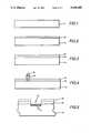
- FIGS. 1-5illustrate a sequence of stages in the production of a metal pattern in accordance with one embodiment of the invention
- FIGS. 6 and 7illustrate a sequence of steps in accordance with another embodiment of the invention.
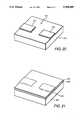
- FIGS. 8-11illustrate a sequence of stages in the fabrication of a pattern in accordance with another embodiment
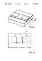
- FIGS. 12-16illustrate stages in another embodiment
- FIGS. 17-19illustrate stages in an electroplating process
- FIGS. 20-22illustrate circuit repair
- FIG. 23illustrates trimming of a resistor to adjust its resistance.
- an electrically insulating substrate 10is shown in cross-section view. It is desired to form a conductor pattern on the upper surface of this substrate.
- This substratemay be glass, polymer materials or other relatively thermally inefficient materials.
- thermally inefficientwe mean that the material is relatively slow to dissipate localized heat. In this sense, this substrate is distinct from such substrates as alumina and the high thermal conductivity metals such as copper which dissipate heat much more rapidly.
- the dividing line between thermally efficient and thermally inefficient materialsis in part dependent on the energy of the laser beam used to pattern the metal.
- a first layer of a thermally inefficient metal 22is formed on the upper surface of the substrate 10 to provide the structure shown in FIG. 2.
- This metalis preferably titanium, but may instead be chrome, nichrome, nickel, stainless steel, magnesium, manganese and so forth.
- This metalis deposited on the substrate under vacuum or other non-oxidizing conditions by any appropriate method, such as sputtering, thermal evaporation, chemical vapor deposition and so forth. We prefer to deposit this metal layer by sputtering. This layer is preferably from 500 to 1,000 ⁇ thick.
- a layer 24 of a UV light absorbing metalwhich is preferably copper but may also be gold, is deposited on top of the layer 22 without breaking the vacuum in the deposition system to provide the structure illustrated in FIG. 3.
- This copper layermay preferably be deposited to a depth in the range from 500-3,000 ⁇ . While thicker layers can be used where higher laser power is available, this thickness is adequate to the purpose, and effective with a laser power of 1- 2 watts at 351-363 nm. Other wave lengths may be used with other metals having different absorption spectra.
- the substrate with its metal coatingis mounted in a laser delivery system which is capable of scanning an intense UV light beam across the substrate.
- argon ion laseroperating at 351 nm, but other frequencies may also be used.
- the laseris then scanned across the surface of the metal 24 in a pattern which corresponds to the areas in which metal is to be removed as illustrated in FIG. 4.
- the copperabsorbs roughly 60% of the UV light incident thereon and is heated to an ablation temperature.
- Direct ablation of the titanium itself without an overlying absorbing layeris not effective because titanium reflects about 81% of incident 351 nm light.
- there is sufficient thermal coupling between the copper and the titaniumthat the laser heating of the copper heats the underlying titanium to an ablation temperature which results in the two metals ablating off the substrate together. We prefer to perform this ablation process in an oxidizing atmosphere.
- This oxidizing atmospheremay be air, air with additional oxygen added to it, pure oxygen, a chlorine containing atmosphere and so forth. We prefer to use air or air plus oxygen.
- the titanium and copperburn as they ablate with a sparkling effect similar to that of Fourth of July sparklers. This sparkling extends substantially above the surface of the metal 24.
- a beneficial side effect of this process where the substrate 10 is a polymeris that the portion of the polymer surface from which the metal is ablated becomes roughened with a surface characteristic which looks much like needles standing on their end. This is illustrated in FIG. 5 where the portion 12 of the substrate surface 10 from which the metal was ablated has needle-like columns 14 extending roughly vertically. In many instances these columns are mushroom shaped with their upper end larger in cross section than their stem or shank. This roughened surface is a substantial advantage in a high density interconnect structure or other structure where a subsequent dielectric layer is later formed over the metal pattern and the exposed portions of the substrate 10.
- thisis an adhesion promoting technique which can be applied to a polymer surface even where none of the deposited metal is to be retained on the polymer and its only function is to enable the roughening of the polymer surface during its ablation. This results in a greatly increased surface area.
- chrome used as the first or lower metal layerproduces a similar sparkling and improvement in pattern definition.
- chrome used as the first or lower metal layerproduces a similar sparkling and improvement in pattern definition.
- nickel, stainless steel, magnesium, manganese and similar metalswhich are or contain highly reactive elements will produce similar sparkling and improvement in pattern definition.
- a layer 32 of such a UV light absorbing metalmay be deposited directly on the substrate 10, as illustrated in FIG. 6.
- the layer 32is then patterned by use of laser ablation in the same manner as described above to selectively remove the metal 32 from the surface of the substrate 10 to produce the structure shown schematically in FIG. 7.
- the resulting patternis poorer and the substrate surface may remain conductive in the ablated regions where the substrate is a polymer.
- a thermally inefficient layerbetween the substrate and the ultraviolet UV light absorbing metal in order to enable the laser ablation process to remove the UV light absorbing metal.
- a layer 112 of a thermally inefficient metalis vacuum deposited on a thermally conducting substrate 100 to provide the structure illustrated in FIG. 8.
- This thermally inefficient metalmay be titanium, chromium, stainless steel (as a laminated layer) nichrome, magnesium, manganese or other metals or mixtures or alloys of metals which are thermally inefficient and sufficiently reactive.
- the layer 112is made thick enough to render its upper surface thermally inefficient.
- the poor thermal efficiency of the layer 112insulates an overlying layer from the thermal efficiency of the substrate 100.
- a layer 114 of UV light absorbing metalis vacuum deposited on the thermally inefficient metal 112 without breaking the vacuum in the deposition apparatus to provide the structure shown in FIG. 9.
- the upper metal layer 114protects the lower metal layer 112 from oxidation and other chemical reactions.
- the metal 114is then ablated by a laser beam 126 as illustrated in FIG. 10. This removes the UV light absorbing metal 114 in the laser scan pattern and may also remove part of but not all of the thermally inefficient metal 112.
- At least the lower portion of the thermally inefficient metalremains on the substrate because for a sufficiently thin layer of the thermally inefficient metal, the underlying substrate 100 carries heat away so rapidly that the thermally inefficient layer cannot be heated to an ablation temperature.
- the retained portions of that upper metal layermay be used as a mask for chemically etching the now exposed portions of the thermally inefficient metal 112 to leave portions 120 of the substrate surface metal-free. After such etching of the exposed portions of layer 112, the structure appears as shown in FIG. 11.
- a four layer metal structuremay be formed prior to laser ablation by successfully depositing titanium, copper, titanium and copper to provide a structure of the general type shown in FIG. 12. These layers may be ⁇ 1000 ⁇ thick titanium, ⁇ 3000 ⁇ of deposited copper on which copper is electroplated to ⁇ 3 mm thick, ⁇ 500-1000 ⁇ thick titanium and ⁇ 500-3000 ⁇ thick copper, respectively. The upper-most copper layer 118 may then be ablated from the upper surface of the upper titanium layer 116 to leave the copper in the desired pattern for the metallization as shown in FIG. 13.
- This ablationis generally non-reactive in that no burning or sparkling occurs and none of the titanium appears to be removed during the ablation where the titanium layer is ⁇ 500-1000 ⁇ thick. However, excellent patterning is obtained. This is believed to be in part a result of the impervious nature of the titanium layer.
- the now exposed portions of the underlying titaniummay then be etched with an HF-based etchant to expose the thick copper layer 114 as shown in FIG. 14. This etchant needs to be one which etches titanium without etching copper.
- a copper etchthen removes the exposed portions of the lower, thick copper layer 14 and the remaining portions of the upper, thin copper layer 118 to provide the structure shown in FIG. 15.
- a final titanium etchremoves the now exposed portions of the lower titanium layer 112 and the portions of the upper titanium layer 116 which protected the copper of the conductor runs during the etching of the thick copper layer 114. This results in the structure shown in FIG. 16.
- copper layer 114may be left with a thickness of ⁇ 6000 ⁇ or so and the layers 116 and 18 deposited thereon.
- the processthen follows that described above through the etching of the upper titanium layer 116.
- the retained portions of the upper copper layer 118are removed from the surface of the titanium by a quick copper etch in ferric chloride which leaves the layer 114 of copper ⁇ 3000 ⁇ thick as shown in FIG. 17.
- Titaniumforms titanium oxide when exposed to air.
- the surface of the upper titanium layer 116is coated with titanium oxide.
- the resulting titanium oxide layeris sufficiently electrically insulating to prevent electroplating on the titanium, that is, the titanium oxide coated titanium acts as a resist for electroplating.
- this structuremay then be electroplated in a copper, gold, chrome or nickel electroplating bath to produce plated conductors having the pattern of the exposed copper 114 without depositing the copper gold, chrome or nickel 122 on the titanium portion of the structure as shown in FIG. 18.
- Thisprovides an effective method of forming gold, chrome or nickel plating on copper without the problems of photoresist lifting which have been experienced in the prior art.
- the surface titanium layermay be removed in a HF-based etchant, the portions of the lower copper layer 114 which are not protected by plated metal 122 may be removed in a ferric chloride etchant and the then unprotected portions of the lower titanium layer may be removed in a HF-based etchant.
- FIG. 19The result is the structure illustrated in FIG. 19 in which electroplated copper, gold, chrome or nickel conductors are provided. While this process is highly effective for copper electroplating, its benefits are more pronounced for gold, chromium and nickel electroplating because copper plating baths attack photoresist much more slowly than gold, chromium and nickel electroplating baths do with the result that prior art electroplating of copper has been much more successful than prior art electroplating of gold, chromium and nickel.
- the substrate 200may be a single layer of insulating material or may be a multilayer printed circuit structure (including high density interconnect structures) having an insulating upper surface on which the two portions 210 and 212 of an open trace are disposed with an unintended gap 214 therebetween.
- a first layer 222 of a thermally inefficient, reactive metal such as titaniumis deposited over the entire upper surface of the substrate 200 and any conductors thereon.
- a second layer 224 of a UV light absorbing metal such as copperis uniformly deposited over the upper surface.
- the entire upper surface of the substrate 200is conductive.
- the deposited metalsare then laser reactive ablated from those portions of the upper surface of the substrate 200 where conductors are not desired, but without ablating the portions of the deposited metals which bridge the gap 214 between the conductors 210 and 212.
- the retained portion of the deposited metals in the vicinity of the gap between the conductors 210 and 212serve as a bridging conductor to close the gap, thereby repairing the structure as shown in FIG. 22.
- This same techniquecan also be used to provide temporary connections for programming during testing or for other purposes. Such temporary connections can then be removed by etching or by further laser ablation.
- a resistor 310is disposed on a substrate 300.
- a two layer metallization 320is disposed on top of the resistor material as its contacts. These contacts can be initially patterned by photoresistmasking and etching. These contacts are then laser ablated to increase the length of the current path through the resistor material between the two contacts to thereby increase the resistance exhibited by the resistor. Alternatively, all of the patterning of these contacts can be done by laser ablation.
Landscapes
- Engineering & Computer Science (AREA)
- Manufacturing & Machinery (AREA)
- Microelectronics & Electronic Packaging (AREA)
- Physics & Mathematics (AREA)
- Optics & Photonics (AREA)
- Plasma & Fusion (AREA)
- Ceramic Engineering (AREA)
- Condensed Matter Physics & Semiconductors (AREA)
- General Physics & Mathematics (AREA)
- Computer Hardware Design (AREA)
- Power Engineering (AREA)
- Metallurgy (AREA)
- Mechanical Engineering (AREA)
- Manufacturing Of Printed Wiring (AREA)
- Laser Beam Processing (AREA)
- Parts Printed On Printed Circuit Boards (AREA)
- Apparatuses And Processes For Manufacturing Resistors (AREA)
- Manufacturing Of Printed Circuit Boards (AREA)
Abstract
Description
Claims (26)
Priority Applications (4)
| Application Number | Priority Date | Filing Date | Title |
|---|---|---|---|
| US07/597,255US5104480A (en) | 1990-10-12 | 1990-10-12 | Direct patterning of metals over a thermally inefficient surface using a laser |
| JP28202991AJP3338465B2 (en) | 1990-10-12 | 1991-10-03 | Direct patterning of metals on thermally inefficient surfaces by using a laser |
| EP91309278AEP0480703B1 (en) | 1990-10-12 | 1991-10-09 | Producing metal patterns on a substrate |
| DE69125333TDE69125333T2 (en) | 1990-10-12 | 1991-10-09 | Making metal patterns on a substrate |
Applications Claiming Priority (1)
| Application Number | Priority Date | Filing Date | Title |
|---|---|---|---|
| US07/597,255US5104480A (en) | 1990-10-12 | 1990-10-12 | Direct patterning of metals over a thermally inefficient surface using a laser |
Publications (1)
| Publication Number | Publication Date |
|---|---|
| US5104480Atrue US5104480A (en) | 1992-04-14 |
Family
ID=24390748
Family Applications (1)
| Application Number | Title | Priority Date | Filing Date |
|---|---|---|---|
| US07/597,255Expired - LifetimeUS5104480A (en) | 1990-10-12 | 1990-10-12 | Direct patterning of metals over a thermally inefficient surface using a laser |
Country Status (4)
| Country | Link |
|---|---|
| US (1) | US5104480A (en) |
| EP (1) | EP0480703B1 (en) |
| JP (1) | JP3338465B2 (en) |
| DE (1) | DE69125333T2 (en) |
Cited By (54)
| Publication number | Priority date | Publication date | Assignee | Title |
|---|---|---|---|---|
| US5505320A (en)* | 1994-11-22 | 1996-04-09 | International Business Machines Corporation | Method employing laser ablating for providing a pattern on a substrate |
| US5535903A (en)* | 1994-03-16 | 1996-07-16 | Fujitsu Limited | Method for breaking conducting path formed on or in printed-circuit board and laser system for using the method |
| US5567329A (en)* | 1995-01-27 | 1996-10-22 | Martin Marietta Corporation | Method and system for fabricating a multilayer laminate for a printed wiring board, and a printed wiring board formed thereby |
| US5575930A (en)* | 1992-10-07 | 1996-11-19 | Tietje-Girault; Jordis | Method of making gas permeable membranes for amperometric gas electrodes |
| US5821505A (en)* | 1997-04-04 | 1998-10-13 | Unisys Corporation | Temperature control system for an electronic device which achieves a quick response by interposing a heater between the device and a heat sink |
| EP0877417A1 (en)* | 1997-05-09 | 1998-11-11 | Lucent Technologies Inc. | Method for fabrication of electrodes and other electrically-conductive structures |
| US6261941B1 (en)* | 1998-02-12 | 2001-07-17 | Georgia Tech Research Corp. | Method for manufacturing a multilayer wiring substrate |
| US6388230B1 (en)* | 1999-10-13 | 2002-05-14 | Morton International, Inc. | Laser imaging of thin layer electronic circuitry material |
| WO2002060633A1 (en)* | 2001-02-01 | 2002-08-08 | Electro Scientific Industries, Inc. | Resistor trimming with small uniform spot from solid-state uv laser |
| US20020170897A1 (en)* | 2001-05-21 | 2002-11-21 | Hall Frank L. | Methods for preparing ball grid array substrates via use of a laser |
| US6528869B1 (en) | 2001-04-06 | 2003-03-04 | Amkor Technology, Inc. | Semiconductor package with molded substrate and recessed input/output terminals |
| US6534743B2 (en)* | 2001-02-01 | 2003-03-18 | Electro Scientific Industries, Inc. | Resistor trimming with small uniform spot from solid-state UV laser |
| US20030094367A1 (en)* | 2000-11-01 | 2003-05-22 | Bhullar Raghbir S. | Biosensor |
| US6586826B1 (en) | 2001-06-13 | 2003-07-01 | Amkor Technology, Inc. | Integrated circuit package having posts for connection to other packages and substrates |
| US20030178302A1 (en)* | 2002-03-21 | 2003-09-25 | Bhullar Raghbir S. | Biosensor |
| US20030196891A1 (en)* | 2002-03-15 | 2003-10-23 | Kabushiki Kaisha Toyota Chuo Kenkyusho | Process for reforming surface of substrate, reformed substrate and apparatus for the same |
| US6645359B1 (en) | 2000-10-06 | 2003-11-11 | Roche Diagnostics Corporation | Biosensor |
| US6662439B1 (en) | 1999-10-04 | 2003-12-16 | Roche Diagnostics Corporation | Laser defined features for patterned laminates and electrodes |
| US20040009618A1 (en)* | 2002-03-27 | 2004-01-15 | Couch Bruce L. | Method and system for high-speed, precise micromachining an array of devices |
| US20040056330A1 (en)* | 2002-09-23 | 2004-03-25 | International Business Machines Corporation | Fine line circuitization |
| US20040069636A1 (en)* | 2001-03-07 | 2004-04-15 | Heinrich Meyer | Metal pattern formation |
| US20040091588A1 (en)* | 2002-10-31 | 2004-05-13 | Xiaochun Li | Food processing apparatus and method |
| US20040173894A1 (en)* | 2001-09-27 | 2004-09-09 | Amkor Technology, Inc. | Integrated circuit package including interconnection posts for multiple electrical connections |
| US20040194302A1 (en)* | 1999-10-04 | 2004-10-07 | Bhullar Raghbir S. | Method of making a biosensor |
| US6819349B2 (en)* | 2000-11-14 | 2004-11-16 | Toto Ltd. | Mark forming method and product using the same method |
| US20060071303A1 (en)* | 2004-10-06 | 2006-04-06 | Chung-Sun Lee | Film substrate of a semiconductor package and a manufacturing method |
| US20060099731A1 (en)* | 2002-10-16 | 2006-05-11 | Microemissive Displays Limited | Method of patterning a functional material on to a substrate |
| WO2006100202A1 (en)* | 2005-03-23 | 2006-09-28 | Technische Universität Ilmenau | Method for laser microstructuring a material using a protective layer with a threshold intensity defined by reflection and absorption characteristics |
| US20070092128A1 (en)* | 2005-10-21 | 2007-04-26 | Orbotech Ltd | Automatic repair of electric circuits |
| US20070138153A1 (en)* | 2005-12-20 | 2007-06-21 | Redman Dean E | Wide web laser ablation |
| US20070148206A1 (en)* | 2005-12-22 | 2007-06-28 | The Penn State Research Foundation | Method and systems for forming and using nanoengineered sculptured thin films |
| US20070178714A1 (en)* | 2002-03-27 | 2007-08-02 | Bo Gu | Method and system for high-speed precise laser trimming and scan lens for use therein |
| US20070215575A1 (en)* | 2006-03-15 | 2007-09-20 | Bo Gu | Method and system for high-speed, precise, laser-based modification of one or more electrical elements |
| US20080314882A1 (en)* | 2001-08-29 | 2008-12-25 | Bhullar Raghbir S | Method of making a biosensor |
| US20090020502A1 (en)* | 1999-10-04 | 2009-01-22 | Bhullar Raghbir S | Biosensor and method of making |
| US7510985B1 (en) | 2005-10-26 | 2009-03-31 | Lpkf Laser & Electronics Ag | Method to manufacture high-precision RFID straps and RFID antennas using a laser |
| US20090257056A1 (en)* | 2007-04-24 | 2009-10-15 | The Government Of The United States Of America, As Represented By The Secretary Of The Navy | Surface enhanced raman detection on metalized nanostructured polymer films |
| US20090321257A1 (en)* | 2008-06-24 | 2009-12-31 | Yoshifumi Takahara | Biosensor, method of producing the same and detection system comprising the same |
| US20100159268A1 (en)* | 2005-06-21 | 2010-06-24 | Andreas Fath | Method for producing decorative surface structures |
| US20100263921A1 (en)* | 2007-11-05 | 2010-10-21 | Panasonic Electric Works Co., Ltd. | Circuit board and method of manufacturing the same |
| US20100294352A1 (en)* | 2009-05-20 | 2010-11-25 | Uma Srinivasan | Metal patterning for electrically conductive structures based on alloy formation |
| US7892849B2 (en) | 2003-06-20 | 2011-02-22 | Roche Diagnostics Operations, Inc. | Reagent stripe for test strip |
| CN102214539A (en)* | 2010-04-08 | 2011-10-12 | 旭硝子株式会社 | Process for producing substrate provided with metal pattern and substrate provided with metal laminate |
| US8593727B2 (en) | 2011-04-25 | 2013-11-26 | Vladimir G. Kozlov | Single-shot laser ablation of a metal film on a polymer membrane |
| US20150173202A1 (en)* | 2012-06-07 | 2015-06-18 | Rmt Limited | Method for producing conductive tracks |
| US20150298124A1 (en)* | 2014-04-16 | 2015-10-22 | Abbott Laboratories | Droplet actuator fabrication apparatus, systems, and related methods |
| CN105023848A (en)* | 2014-04-30 | 2015-11-04 | 启碁科技股份有限公司 | Substrate structure and manufacturing method thereof |
| US20160315295A1 (en)* | 2013-12-19 | 2016-10-27 | The Swatch Group Research And Development Ltd | Battery with a non-conductive structured surface |
| US9842740B2 (en) | 2014-08-29 | 2017-12-12 | Seagate Technology Llc | Ablation for feature recovery |
| US9942982B2 (en) | 1997-08-04 | 2018-04-10 | Continental Circuits, Llc | Electrical device with teeth joining layers and method for making the same |
| US10537027B2 (en) | 2013-08-02 | 2020-01-14 | Orbotech Ltd. | Method producing a conductive path on a substrate |
| CN111343793A (en)* | 2020-03-12 | 2020-06-26 | 电子科技大学 | A method for metallizing the surface of a printed circuit composite dielectric substrate |
| US11302462B2 (en) | 2018-06-25 | 2022-04-12 | Vishay Electronic Gmbh | Method for producing a plurality of resistance modular units over a ceramic substrate |
| US11390941B2 (en)* | 2017-04-07 | 2022-07-19 | Byoung Sam Kim | Manufacturing method of radio wave transmittable sensor cover having micro crack and laser hole and radio wave transmittable sensor cover manufactured using the same |
Families Citing this family (11)
| Publication number | Priority date | Publication date | Assignee | Title |
|---|---|---|---|---|
| US6518088B1 (en) | 1994-09-23 | 2003-02-11 | Siemens N.V. And Interuniversitair Micro-Electronica Centrum Vzw | Polymer stud grid array |
| EP0971405A3 (en)* | 1994-09-23 | 2000-05-10 | Siemens S.A. | Method for manufacturing a substrate for a polymer stud grid array |
| US6350555B1 (en) | 1998-01-14 | 2002-02-26 | Precision Coatings, Inc. | Direct write imaging medium |
| DE19913367C1 (en)* | 1999-03-24 | 2000-12-14 | Siemens Ag | Method of making an electrical circuit |
| US6462629B1 (en)* | 1999-06-15 | 2002-10-08 | Cts Corporation | Ablative RF ceramic block filters |
| FR2795907B1 (en)* | 1999-07-01 | 2007-02-16 | Gemplus Card Int | PROCESS FOR THE MANUFACTURE AND TESTING OF ELECTRONIC MICROMODULAS, IN PARTICULAR FOR CHIP CARDS |
| US6559735B1 (en) | 2000-10-31 | 2003-05-06 | Cts Corporation | Duplexer filter with an alternative signal path |
| US6571468B1 (en) | 2001-02-26 | 2003-06-03 | Saturn Electronics & Engineering, Inc. | Traceless flip chip assembly and method |
| JP4639975B2 (en)* | 2005-06-07 | 2011-02-23 | パナソニック電工株式会社 | Manufacturing method of three-dimensional circuit board |
| KR20070004373A (en)* | 2005-07-04 | 2007-01-09 | 삼성전자주식회사 | Built-in antenna pattern of mobile terminal and manufacturing method thereof |
| CA2972577A1 (en) | 2014-12-31 | 2016-07-07 | Abbott Laboratories | Digital microfluidic dilution apparatus, systems, and related methods |
Citations (4)
| Publication number | Priority date | Publication date | Assignee | Title |
|---|---|---|---|---|
| US3867217A (en)* | 1973-10-29 | 1975-02-18 | Bell Telephone Labor Inc | Methods for making electronic circuits |
| US4037075A (en)* | 1974-05-16 | 1977-07-19 | Crosfield Electronics Limited | Image reproduction systems |
| US4259433A (en)* | 1976-10-22 | 1981-03-31 | Fuji Photo Film Co., Ltd. | Method for producing disk-recording plates |
| US4874920A (en)* | 1984-06-08 | 1989-10-17 | Semiconductor Energy Laboratory Co., Ltd. | Electronic device manufacturing methods |
Family Cites Families (3)
| Publication number | Priority date | Publication date | Assignee | Title |
|---|---|---|---|---|
| JPS61108195A (en)* | 1984-11-01 | 1986-05-26 | インタ−ナショナル ビジネス マシ−ンズ コ−ポレ−ション | Formation of electrically continued layers on substrate |
| US4786358A (en)* | 1986-08-08 | 1988-11-22 | Semiconductor Energy Laboratory Co., Ltd. | Method for forming a pattern of a film on a substrate with a laser beam |
| US4826785A (en)* | 1987-01-27 | 1989-05-02 | Inmos Corporation | Metallic fuse with optically absorptive layer |
- 1990
- 1990-10-12USUS07/597,255patent/US5104480A/ennot_activeExpired - Lifetime
- 1991
- 1991-10-03JPJP28202991Apatent/JP3338465B2/ennot_activeExpired - Fee Related
- 1991-10-09EPEP91309278Apatent/EP0480703B1/ennot_activeExpired - Lifetime
- 1991-10-09DEDE69125333Tpatent/DE69125333T2/ennot_activeExpired - Fee Related
Patent Citations (4)
| Publication number | Priority date | Publication date | Assignee | Title |
|---|---|---|---|---|
| US3867217A (en)* | 1973-10-29 | 1975-02-18 | Bell Telephone Labor Inc | Methods for making electronic circuits |
| US4037075A (en)* | 1974-05-16 | 1977-07-19 | Crosfield Electronics Limited | Image reproduction systems |
| US4259433A (en)* | 1976-10-22 | 1981-03-31 | Fuji Photo Film Co., Ltd. | Method for producing disk-recording plates |
| US4874920A (en)* | 1984-06-08 | 1989-10-17 | Semiconductor Energy Laboratory Co., Ltd. | Electronic device manufacturing methods |
Cited By (108)
| Publication number | Priority date | Publication date | Assignee | Title |
|---|---|---|---|---|
| US5575930A (en)* | 1992-10-07 | 1996-11-19 | Tietje-Girault; Jordis | Method of making gas permeable membranes for amperometric gas electrodes |
| US5535903A (en)* | 1994-03-16 | 1996-07-16 | Fujitsu Limited | Method for breaking conducting path formed on or in printed-circuit board and laser system for using the method |
| US5505320A (en)* | 1994-11-22 | 1996-04-09 | International Business Machines Corporation | Method employing laser ablating for providing a pattern on a substrate |
| US5567329A (en)* | 1995-01-27 | 1996-10-22 | Martin Marietta Corporation | Method and system for fabricating a multilayer laminate for a printed wiring board, and a printed wiring board formed thereby |
| US5821505A (en)* | 1997-04-04 | 1998-10-13 | Unisys Corporation | Temperature control system for an electronic device which achieves a quick response by interposing a heater between the device and a heat sink |
| EP0877417A1 (en)* | 1997-05-09 | 1998-11-11 | Lucent Technologies Inc. | Method for fabrication of electrodes and other electrically-conductive structures |
| US9942982B2 (en) | 1997-08-04 | 2018-04-10 | Continental Circuits, Llc | Electrical device with teeth joining layers and method for making the same |
| US6261941B1 (en)* | 1998-02-12 | 2001-07-17 | Georgia Tech Research Corp. | Method for manufacturing a multilayer wiring substrate |
| US8551308B2 (en) | 1999-10-04 | 2013-10-08 | Roche Diagnostics Operations, Inc. | Biosensor and method of making |
| US20040194302A1 (en)* | 1999-10-04 | 2004-10-07 | Bhullar Raghbir S. | Method of making a biosensor |
| US20090056120A1 (en)* | 1999-10-04 | 2009-03-05 | Bhullar Raghbir S | Biosensor and method of making |
| US7073246B2 (en)* | 1999-10-04 | 2006-07-11 | Roche Diagnostics Operations, Inc. | Method of making a biosensor |
| US7386937B2 (en) | 1999-10-04 | 2008-06-17 | Roche Diagnostics Operations, Inc. | Method of making a biosensor |
| US8287703B2 (en) | 1999-10-04 | 2012-10-16 | Roche Diagnostics Operations, Inc. | Biosensor and method of making |
| US6662439B1 (en) | 1999-10-04 | 2003-12-16 | Roche Diagnostics Corporation | Laser defined features for patterned laminates and electrodes |
| US20090020502A1 (en)* | 1999-10-04 | 2009-01-22 | Bhullar Raghbir S | Biosensor and method of making |
| US6388230B1 (en)* | 1999-10-13 | 2002-05-14 | Morton International, Inc. | Laser imaging of thin layer electronic circuitry material |
| US7287318B2 (en) | 2000-10-06 | 2007-10-30 | Roche Diagnostics Operations, Inc. | Biosensor |
| US6645359B1 (en) | 2000-10-06 | 2003-11-11 | Roche Diagnostics Corporation | Biosensor |
| US20040163953A1 (en)* | 2000-10-06 | 2004-08-26 | Bhullar Raghbir S. | Biosensor |
| US20030094367A1 (en)* | 2000-11-01 | 2003-05-22 | Bhullar Raghbir S. | Biosensor |
| US6911621B2 (en) | 2000-11-01 | 2005-06-28 | Roche Diagnostics Corporation | Biosensor |
| US6819349B2 (en)* | 2000-11-14 | 2004-11-16 | Toto Ltd. | Mark forming method and product using the same method |
| US6534743B2 (en)* | 2001-02-01 | 2003-03-18 | Electro Scientific Industries, Inc. | Resistor trimming with small uniform spot from solid-state UV laser |
| GB2389555A (en)* | 2001-02-01 | 2003-12-17 | Electro Scient Ind Inc | Resistor trimming with small uniform spot from solid-state UV laser |
| WO2002060633A1 (en)* | 2001-02-01 | 2002-08-08 | Electro Scientific Industries, Inc. | Resistor trimming with small uniform spot from solid-state uv laser |
| US20040069636A1 (en)* | 2001-03-07 | 2004-04-15 | Heinrich Meyer | Metal pattern formation |
| CN1305120C (en)* | 2001-03-07 | 2007-03-14 | 埃托特克德国有限公司 | Forming of metal patterns |
| US6528869B1 (en) | 2001-04-06 | 2003-03-04 | Amkor Technology, Inc. | Semiconductor package with molded substrate and recessed input/output terminals |
| US20050170658A1 (en)* | 2001-05-21 | 2005-08-04 | Hall Frank L. | Methods for preparing ball grid array substrates via use of a laser |
| US20060113291A1 (en)* | 2001-05-21 | 2006-06-01 | Hall Frank L | Method for preparing ball grid array substrates via use of a laser |
| US20040170915A1 (en)* | 2001-05-21 | 2004-09-02 | Hall Frank L. | Methods for preparing ball grid array substrates via use of a laser |
| US20060249494A1 (en)* | 2001-05-21 | 2006-11-09 | Hall Frank L | Methods for preparing ball grid array substrates via use of a laser |
| US20060249492A1 (en)* | 2001-05-21 | 2006-11-09 | Hall Frank L | Methods for preparing ball grid array substrates via use of a laser |
| US20060249493A1 (en)* | 2001-05-21 | 2006-11-09 | Hall Frank L | Methods for preparing ball grid array substrates via use of a laser |
| US20060249495A1 (en)* | 2001-05-21 | 2006-11-09 | Hall Frank L | Methods for preparing ball grid array substrates via use of a laser |
| US20040104206A1 (en)* | 2001-05-21 | 2004-06-03 | Hall Frank L. | Methods for preparing ball grid array substrates via use of a laser |
| US20020170897A1 (en)* | 2001-05-21 | 2002-11-21 | Hall Frank L. | Methods for preparing ball grid array substrates via use of a laser |
| US20040169024A1 (en)* | 2001-05-21 | 2004-09-02 | Hall Frank L. | Methods for preparing ball grid array substrates via use of a laser |
| US20060163573A1 (en)* | 2001-05-21 | 2006-07-27 | Hall Frank L | Method for preparing ball grid array substrates via use of a laser |
| US6586826B1 (en) | 2001-06-13 | 2003-07-01 | Amkor Technology, Inc. | Integrated circuit package having posts for connection to other packages and substrates |
| US20100219071A1 (en)* | 2001-08-29 | 2010-09-02 | Bhullar Raghbir S | Biosensor |
| US20080314882A1 (en)* | 2001-08-29 | 2008-12-25 | Bhullar Raghbir S | Method of making a biosensor |
| US7476827B1 (en) | 2001-08-29 | 2009-01-13 | Roche Diagnostics Operations, Inc. | Method of making a biosensor |
| US7780827B1 (en) | 2001-08-29 | 2010-08-24 | Roche Diagnostics Operations, Inc. | Biosensor |
| US20040173894A1 (en)* | 2001-09-27 | 2004-09-09 | Amkor Technology, Inc. | Integrated circuit package including interconnection posts for multiple electrical connections |
| US20030196891A1 (en)* | 2002-03-15 | 2003-10-23 | Kabushiki Kaisha Toyota Chuo Kenkyusho | Process for reforming surface of substrate, reformed substrate and apparatus for the same |
| US6858115B2 (en) | 2002-03-15 | 2005-02-22 | Kabushiki Kaisha Toyota Chuo Kenkyusho | Process for reforming surface of substrate, reformed substrate and apparatus for the same |
| US20030178302A1 (en)* | 2002-03-21 | 2003-09-25 | Bhullar Raghbir S. | Biosensor |
| US20050136471A1 (en)* | 2002-03-21 | 2005-06-23 | Bhullar Raghbir S. | Biosensor |
| US6866758B2 (en) | 2002-03-21 | 2005-03-15 | Roche Diagnostics Corporation | Biosensor |
| US20040009618A1 (en)* | 2002-03-27 | 2004-01-15 | Couch Bruce L. | Method and system for high-speed, precise micromachining an array of devices |
| US7407861B2 (en) | 2002-03-27 | 2008-08-05 | Gsi Group Corporation | Method and system for high-speed, precise micromachining an array of devices |
| US6951995B2 (en) | 2002-03-27 | 2005-10-04 | Gsi Lumonics Corp. | Method and system for high-speed, precise micromachining an array of devices |
| US20050233537A1 (en)* | 2002-03-27 | 2005-10-20 | Gsi Lumonics Corporation | Method and system for high-speed, precise micromachining an array of devices |
| US7871903B2 (en) | 2002-03-27 | 2011-01-18 | Gsi Group Corporation | Method and system for high-speed, precise micromachining an array of devices |
| US20070178714A1 (en)* | 2002-03-27 | 2007-08-02 | Bo Gu | Method and system for high-speed precise laser trimming and scan lens for use therein |
| US20060205121A1 (en)* | 2002-03-27 | 2006-09-14 | Gsi Lumonics Corporation | Method and system for high-speed, precise micromachining an array of devices |
| US7563695B2 (en) | 2002-03-27 | 2009-07-21 | Gsi Group Corporation | Method and system for high-speed precise laser trimming and scan lens for use therein |
| US20040056330A1 (en)* | 2002-09-23 | 2004-03-25 | International Business Machines Corporation | Fine line circuitization |
| US7325299B2 (en) | 2002-09-23 | 2008-02-05 | International Business Machines Corporation | Method of making a circuitized substrate |
| US7596862B2 (en) | 2002-09-23 | 2009-10-06 | International Business Machines Corporation | Method of making a circuitized substrate |
| US20080014409A1 (en)* | 2002-09-23 | 2008-01-17 | Egitto Frank D | Method of making a circuitized substrate |
| US7185428B2 (en)* | 2002-09-23 | 2007-03-06 | International Business Machines Corporation | Method of making a circuitized substrate |
| US20070102396A1 (en)* | 2002-09-23 | 2007-05-10 | Egitto Frank D | Method of making a circuitized substrate |
| US6822332B2 (en) | 2002-09-23 | 2004-11-23 | International Business Machines Corporation | Fine line circuitization |
| US20040130003A1 (en)* | 2002-09-23 | 2004-07-08 | International Business Machines Corporation | Fine line circuitization |
| US20060099731A1 (en)* | 2002-10-16 | 2006-05-11 | Microemissive Displays Limited | Method of patterning a functional material on to a substrate |
| US20040091588A1 (en)* | 2002-10-31 | 2004-05-13 | Xiaochun Li | Food processing apparatus and method |
| US7892849B2 (en) | 2003-06-20 | 2011-02-22 | Roche Diagnostics Operations, Inc. | Reagent stripe for test strip |
| US20060071303A1 (en)* | 2004-10-06 | 2006-04-06 | Chung-Sun Lee | Film substrate of a semiconductor package and a manufacturing method |
| WO2006100202A1 (en)* | 2005-03-23 | 2006-09-28 | Technische Universität Ilmenau | Method for laser microstructuring a material using a protective layer with a threshold intensity defined by reflection and absorption characteristics |
| US20100159268A1 (en)* | 2005-06-21 | 2010-06-24 | Andreas Fath | Method for producing decorative surface structures |
| US8290239B2 (en) | 2005-10-21 | 2012-10-16 | Orbotech Ltd. | Automatic repair of electric circuits |
| US20070092128A1 (en)* | 2005-10-21 | 2007-04-26 | Orbotech Ltd | Automatic repair of electric circuits |
| US7510985B1 (en) | 2005-10-26 | 2009-03-31 | Lpkf Laser & Electronics Ag | Method to manufacture high-precision RFID straps and RFID antennas using a laser |
| US20070138153A1 (en)* | 2005-12-20 | 2007-06-21 | Redman Dean E | Wide web laser ablation |
| US20070148206A1 (en)* | 2005-12-22 | 2007-06-28 | The Penn State Research Foundation | Method and systems for forming and using nanoengineered sculptured thin films |
| US8647654B2 (en) | 2005-12-22 | 2014-02-11 | The Penn State Research Foundation | Method and systems for forming and using nanoengineered sculptured thin films |
| US20070215575A1 (en)* | 2006-03-15 | 2007-09-20 | Bo Gu | Method and system for high-speed, precise, laser-based modification of one or more electrical elements |
| US20090257056A1 (en)* | 2007-04-24 | 2009-10-15 | The Government Of The United States Of America, As Represented By The Secretary Of The Navy | Surface enhanced raman detection on metalized nanostructured polymer films |
| US8652632B2 (en) | 2007-04-24 | 2014-02-18 | The United States Of America, As Represented By The Secretary Of The Navy | Surface enhanced raman detection on metalized nanostructured polymer films |
| US8338716B2 (en) | 2007-11-05 | 2012-12-25 | Panasonic Corporation | Circuit board and method of manufacturing the same |
| US20100263921A1 (en)* | 2007-11-05 | 2010-10-21 | Panasonic Electric Works Co., Ltd. | Circuit board and method of manufacturing the same |
| WO2009149152A1 (en)* | 2008-06-03 | 2009-12-10 | The Government Of The United States Of America, As Represented By The Secretary Of The Navy | Surface enhanced raman detection on metallized nanostructured polymer films |
| US20090321257A1 (en)* | 2008-06-24 | 2009-12-31 | Yoshifumi Takahara | Biosensor, method of producing the same and detection system comprising the same |
| US9046479B2 (en) | 2008-06-24 | 2015-06-02 | Panasonic Healthcare Holdings Co., Ltd. | Biosensor, method of producing the same and detection system comprising the same |
| US20100294352A1 (en)* | 2009-05-20 | 2010-11-25 | Uma Srinivasan | Metal patterning for electrically conductive structures based on alloy formation |
| US20110249340A1 (en)* | 2010-04-08 | 2011-10-13 | Asahi Glass Company, Limited | Process for producing substrate provided with metal pattern and substrate provided with metal laminate |
| CN102214539A (en)* | 2010-04-08 | 2011-10-12 | 旭硝子株式会社 | Process for producing substrate provided with metal pattern and substrate provided with metal laminate |
| US8648278B2 (en)* | 2010-04-08 | 2014-02-11 | Asahi Glass Company, Limited | Process for producing substrate provided with metal pattern and substrate provided with metal laminate |
| US8593727B2 (en) | 2011-04-25 | 2013-11-26 | Vladimir G. Kozlov | Single-shot laser ablation of a metal film on a polymer membrane |
| US9332648B2 (en)* | 2012-06-07 | 2016-05-03 | Rmt Limited | Method for producing conductive tracks |
| US20150173202A1 (en)* | 2012-06-07 | 2015-06-18 | Rmt Limited | Method for producing conductive tracks |
| US10537027B2 (en) | 2013-08-02 | 2020-01-14 | Orbotech Ltd. | Method producing a conductive path on a substrate |
| US10777780B2 (en)* | 2013-12-19 | 2020-09-15 | The Swatch Group Research And Development Ltd | Battery with a non-conductive structured surface |
| US20160315295A1 (en)* | 2013-12-19 | 2016-10-27 | The Swatch Group Research And Development Ltd | Battery with a non-conductive structured surface |
| US10913064B2 (en)* | 2014-04-16 | 2021-02-09 | Abbott Laboratories | Droplet actuator fabrication apparatus, systems, and related methods |
| CN108656746A (en)* | 2014-04-16 | 2018-10-16 | 雅培制药有限公司 | Droplet actuator manufacturing device, system and correlation technique |
| US20150298124A1 (en)* | 2014-04-16 | 2015-10-22 | Abbott Laboratories | Droplet actuator fabrication apparatus, systems, and related methods |
| US12201980B2 (en) | 2014-04-16 | 2025-01-21 | Abbott Laboratories | Droplet actuator fabrication apparatus, systems, and related methods |
| CN105023848A (en)* | 2014-04-30 | 2015-11-04 | 启碁科技股份有限公司 | Substrate structure and manufacturing method thereof |
| US10087527B2 (en) | 2014-04-30 | 2018-10-02 | Wistron Neweb Corp. | Method of fabricating substrate structure and substrate structure fabricated by the same method |
| CN105023848B (en)* | 2014-04-30 | 2017-12-22 | 启碁科技股份有限公司 | Substrate structure and manufacturing method thereof |
| US9842740B2 (en) | 2014-08-29 | 2017-12-12 | Seagate Technology Llc | Ablation for feature recovery |
| US11390941B2 (en)* | 2017-04-07 | 2022-07-19 | Byoung Sam Kim | Manufacturing method of radio wave transmittable sensor cover having micro crack and laser hole and radio wave transmittable sensor cover manufactured using the same |
| US11302462B2 (en) | 2018-06-25 | 2022-04-12 | Vishay Electronic Gmbh | Method for producing a plurality of resistance modular units over a ceramic substrate |
| CN111343793A (en)* | 2020-03-12 | 2020-06-26 | 电子科技大学 | A method for metallizing the surface of a printed circuit composite dielectric substrate |
Also Published As
| Publication number | Publication date |
|---|---|
| JPH04280494A (en) | 1992-10-06 |
| EP0480703B1 (en) | 1997-03-26 |
| DE69125333D1 (en) | 1997-04-30 |
| EP0480703A3 (en) | 1992-06-03 |
| JP3338465B2 (en) | 2002-10-28 |
| DE69125333T2 (en) | 1997-10-02 |
| EP0480703A2 (en) | 1992-04-15 |
Similar Documents
| Publication | Publication Date | Title |
|---|---|---|
| US5104480A (en) | Direct patterning of metals over a thermally inefficient surface using a laser | |
| JP3587884B2 (en) | Method for manufacturing multilayer circuit board | |
| US5302547A (en) | Systems for patterning dielectrics by laser ablation | |
| US5747358A (en) | Method of forming raised metallic contacts on electrical circuits | |
| US4258468A (en) | Forming vias through multilayer circuit boards | |
| JP3361556B2 (en) | Method of forming circuit wiring pattern | |
| US6119335A (en) | Method for manufacturing multi-layer printed circuit board | |
| US5107586A (en) | Method for interconnecting a stack of integrated circuits at a very high density | |
| US5073814A (en) | Multi-sublayer dielectric layers | |
| EP0366259B1 (en) | A process for interconnecting thin-film electrical circuits | |
| US4704304A (en) | Method for repair of opens in thin film lines on a substrate | |
| EP0206337B1 (en) | Multilayer wiring substrate with engineering change pads | |
| EP0450381B1 (en) | Multilayer interconnection structure | |
| US4983250A (en) | Method of laser patterning an electrical interconnect | |
| US5127998A (en) | Area-selective metallization process | |
| JPH10214920A (en) | Improved type polytetrafluoroethylene thin film chip carrier | |
| US5285571A (en) | Method for extending an electrical conductor over an edge of an HDI substrate | |
| US5230965A (en) | High density interconnect with electroplated conductors | |
| WO1989002697A1 (en) | Induced metallization process by way of dissociating aluminum nitride ceramic | |
| US5550325A (en) | Printed-circuit board including circuit pattern having location to be cut if necessary | |
| JPH07202424A (en) | Production of multilayer wiring board | |
| JP3154964B2 (en) | Printed circuit board and its laser drilling method | |
| GB2307351A (en) | Printed circuit boards and their manufacture | |
| JP3136682B2 (en) | Method for manufacturing multilayer wiring board | |
| JPH0590763A (en) | Printed wiring board and its manufacture |
Legal Events
| Date | Code | Title | Description |
|---|---|---|---|
| AS | Assignment | Owner name:GENERAL ELECTRIC COMPANY, A NY CORP., NEW YORK Free format text:ASSIGNMENT OF ASSIGNORS INTEREST.;ASSIGNORS:WOJNAROWSKI, ROBERT J.;EICHELBERGER, CHARLES W.;REEL/FRAME:005484/0593;SIGNING DATES FROM 19901005 TO 19901009 | |
| FEPP | Fee payment procedure | Free format text:PAYOR NUMBER ASSIGNED (ORIGINAL EVENT CODE: ASPN); ENTITY STATUS OF PATENT OWNER: LARGE ENTITY | |
| STCF | Information on status: patent grant | Free format text:PATENTED CASE | |
| FEPP | Fee payment procedure | Free format text:PAYOR NUMBER ASSIGNED (ORIGINAL EVENT CODE: ASPN); ENTITY STATUS OF PATENT OWNER: LARGE ENTITY Free format text:PAYER NUMBER DE-ASSIGNED (ORIGINAL EVENT CODE: RMPN); ENTITY STATUS OF PATENT OWNER: LARGE ENTITY | |
| AS | Assignment | Owner name:MARTIN MARIETTA CORPORATION, MARYLAND Free format text:ASSIGNMENT OF ASSIGNORS INTEREST;ASSIGNOR:GENERAL ELECTRIC COMPANY;REEL/FRAME:007046/0736 Effective date:19940322 | |
| FPAY | Fee payment | Year of fee payment:4 | |
| AS | Assignment | Owner name:LOCKHEED MARTIN CORPORATION, MARYLAND Free format text:ASSIGNMENT OF ASSIGNORS INTEREST;ASSIGNOR:MARTIN MARIETTA CORPORATION;REEL/FRAME:008628/0518 Effective date:19960128 | |
| FPAY | Fee payment | Year of fee payment:8 | |
| FEPP | Fee payment procedure | Free format text:PAYOR NUMBER ASSIGNED (ORIGINAL EVENT CODE: ASPN); ENTITY STATUS OF PATENT OWNER: LARGE ENTITY Free format text:PAYER NUMBER DE-ASSIGNED (ORIGINAL EVENT CODE: RMPN); ENTITY STATUS OF PATENT OWNER: LARGE ENTITY | |
| FPAY | Fee payment | Year of fee payment:12 |